servo-controlled active feedback 200 watt class-d ... servo-controlled active feedback 200 watt...
TRANSCRIPT

1
Servo-Controlled Active Feedback 200 Watt Class-D Subwoofer Amplifier Alex Kim (904574640) Thomas LaBella (904566662) John Caldwell (904413202) Preston Taylor (904482345) ECE 4206 Electronic Circuit Design II Electrical and Computer Engineering Virginia Tech May 15, 2009 Instructor: Jason Lai TTh 12:30-1:45

2
Contents
Introduction ..................................................................................................................................... 4
Part I: Power Supply ....................................................................................................................... 5
1. Introduction ............................................................................................................................. 5
2. Specifications .......................................................................................................................... 5
3. Design and Simulations .......................................................................................................... 5
3.1. Input Rectification .......................................................................................................... 5
3.2. Startup Circuit ................................................................................................................. 7
3.3. Isolated Buck Converter Power Stage ............................................................................ 9
3.4. Isolation Transformer.................................................................................................... 10
3.5. Isolated Buck Converter Feedback Loop ...................................................................... 11
3.5.1. Open-Loop Transfer Function .............................................................................. 11
3.5.2. Compensator Design ............................................................................................. 13
3.5.3. Compensator Simulation ....................................................................................... 15
3.5.4. Compensator Implementation ............................................................................... 18
3.6. Leakage Inductor .......................................................................................................... 20
3.7. Isolated Buck Converter Controller .............................................................................. 21
3.8. Auxiliary Power Circuit ................................................................................................ 22
3.9. +/- 15V Outputs ............................................................................................................ 23
4. PCB Layout ........................................................................................................................... 25
5. Board Testing and Revisions ................................................................................................ 26
5.1. Initial Problems ............................................................................................................. 26
5.2. Gate Drive Transformers .............................................................................................. 26
5.3. Leakage Inductance ...................................................................................................... 26
5.4. Isolation Transformer.................................................................................................... 27
5.4.1. Buck Converter Power Stage Revisions ............................................................... 28
5.4.2. Feedback Loop Revisions ..................................................................................... 29
5.4.3. Transformer Waveforms ....................................................................................... 29
5.5. Input Rectification ........................................................................................................ 30
5.6. Controller Chip ............................................................................................................. 31
5.7. Output Voltage .............................................................................................................. 32
5.8. Zero Voltage Switching ................................................................................................ 34
6. Summary and Conclusions ................................................................................................... 36
7. TI Parts Used for Design....................................................................................................... 36
Part II: Class D Amplifier ............................................................................................................. 38
1. Introduction ........................................................................................................................... 38

3
2. Input Stage Design ................................................................................................................ 38
2.1. Triangle Wave Generator Design ................................................................................. 38
2.2. Volume Control Design ................................................................................................ 40
2.3. Input Filter Design ........................................................................................................ 41
2.4. Compensator Design ..................................................................................................... 42
3. Output Stage Design ............................................................................................................. 42
3.1. Gate Driving.................................................................................................................. 42
3.2. Output Filter Design ..................................................................................................... 44
3.3. Accelerometer Feedback ............................................................................................... 46
4. PCB Layout ........................................................................................................................... 49
5. Subwoofer Enclosure Design ................................................................................................ 50
6. Input Stage Implementation .................................................................................................. 50
7. Output Stage Implementation ............................................................................................... 51
8. Feedback Implementation ..................................................................................................... 53
8.1. Feedback Results .......................................................................................................... 54
9. Summary and Conclusion ..................................................................................................... 54
10. TI Parts Used for Design....................................................................................................... 55
Conclusions ................................................................................................................................... 55
Appendix I: Final Schematic ........................................................................................................ 56
Appendix II: PCB Layout ............................................................................................................. 61
Appendix III: Bill of Materials ..................................................................................................... 69
Appendix IV: Device Pictures ...................................................................................................... 73

4
INTRODUCTION The Texas Instruments (TI) Analog Design Contest is an undergraduate competition
sponsored by TI to provide students with experience in the design and fabrication of complex circuits utilizing TI’s products. The competition involves the design and construction of an electronic device using three of TI’s analog integrated circuits or two analog and one digital integrated circuit. In order to compete in this contest, our group proposed the construction of a subwoofer controlled using an active feedback system and powered by a class-D amplifier. The class-D amplifier was to be powered using a switching power supply fed from a common wall outlet. The entire system’s configuration is shown below in Figure 1.
Figure1: Block diagram of entire system including power supply, amplifier, subwoofer and the active feedback system.
While the concept for class D amplifiers was initially developed using vacuum tubes, the
technique has received attention in the last 15-20 years due to the rapid advancement of MOSFET technology. Traditional audio amplifiers operate their output devices in their linear region, making them effectively variable resistors. Because of the conduction losses associated with operating transistors in this manner, these amplifiers are limited in terms of their efficiency. Similar to switching power supplies, class-D amplifiers operate their output devices as switches and output a pulse-width modulated signal to a low-pass filter which then recovers the amplified audio signal. The theoretical efficiency of this configuration is 100%, however in practice class-D amplifiers can be expected to exceed 90% efficiency.
Deviating from a traditional powered subwoofer, we also proposed that active feedback be utilized to reduce the subwoofer’s distortion. Active feedback or “servo control” is a proven method to extend the low frequency response and reduce the distortion of a loudspeaker system. The technique relies upon an accelerometer mounted on the speaker’s cone to provide a negative feedback signal to the amplifier.

5
PART I: POWER SUPPLY
1. INTRODUCTION Our project is to design a high power Class D Amplifier for driving a subwoofer. In
designing such a system we first need to design a robust power stage to meet our amplification demands. This paper will focus on this stage of the design. We will detail the design process as well as the methodology used to produce our final product. We begin with designing the input rectification of the wall voltage and filtering the EMI effects. Our focus next turns to designing the many layers of the power stage. We chose to design an isolated full bridge buck converter to provide the primary output power to the power stage of the amplifier. After calculating the output components we turned to developing a transformer to be used as the isolation in the circuit. With these components designed we next designed the compensator circuit using PLECs. In order for the power stage to function we next needed to design an Auxiliary power center to provide power until the converter turned on fully. After each area of design we tested and/or simulated the results using a variety of methods including PSPICE.
2. SPECIFICATIONS Table 2.1 – List of Circuit Specifications
Parameter Value Input Voltage 90-132 V AC Power Output 200W Primary Power Output Voltage 72V Secondary Power Output Voltage +/- 15V Voltage Ripple <0.5V Current Ripple <20% Switching Frequency 100 kHz
3. DESIGN AND SIMULATIONS
3.1. Input Rectification This switch mode power supply will be plugged directly in the wall, so first the AC wall
voltage needs to be rectified to DC voltage so that it can be used by the converter. First, an off-the-shelf IEC wall plug and EMI filter were chosen, each being able to handle at least 6A. The power supply should never draw more than 3A, but 6A is a pretty standard rating for EMI filters. After the EMI filter, a 3A fuse is used to protect the power supply. 3A was chosen by calculating the expected input current using the worst case input voltage and worst case power supply input power as shown in equation (3.1.1). The input power was calculated by assuming our power supply is outputting 250W at 90% efficiency.
277𝑊𝑊
90𝑉𝑉𝑟𝑟𝑟𝑟𝑟𝑟= 3.08𝐴𝐴 (3.1.1)

6
Next, the KBL04 bridge rectifier was chosen. This rectifier can handle 400V and 4A which
is plenty for this application. After the voltage is rectified, there will be large filter capacitors to provide DC smoothing. When this circuit is first plugged into the wall, the uncharged capacitors will act as a short and draw an immense amount of current which will blow the 3A fuse. To prevent this, a NTC thermistor is used between the rectifier and the filter capacitors. The CL-70 was chosen for this application.
Equation (3.1.2) shows how the filter capacitors were chosen. The frequency here is 120Hz because it is a rectified 60Hz from the wall. The nominal rectified voltage is used along with a maximum current of 3A to determine a 10% voltage ripple.
𝐶𝐶 = 𝐼𝐼
2𝑓𝑓∆𝑉𝑉= 3
2∗120∗0.1∗√2∗120= 736.6𝜇𝜇𝜇𝜇 (3.1.2)
Two 470μF capacitors were chosen to ensure that the voltage ripple will remain below 10%.
For safety reasons, a high impedance resistor needs to be placed in parallel with the capacitors to drain them in order to reduce the risk of 170 volt electrical shock while working on the power supply. It needs to be high impedance so that it consumes very little power while the power supply is on, but low enough impedance so that it will drain the capacitors while the power supply is off. Four 12kΩ 2010 surface mount resistors, each being able to handle 1/2W, were chosen. Equation (3.1.3) shows the estimated time it will take for the capacitor to discharge, and equation (3.1.4) shows the worst case power consumption for all four resistors combined while the power supply is operating.
5𝜏𝜏 = 5𝑅𝑅𝐶𝐶 = 5 ∗ 48000 ∗ 940 ∗ 10−6 = 225.6𝑟𝑟, 𝑜𝑜𝑟𝑟 3.76𝑟𝑟𝑚𝑚𝑚𝑚 (3.1.3)
𝑃𝑃𝑟𝑟𝑚𝑚𝑚𝑚 = 𝑉𝑉𝑟𝑟𝑚𝑚𝑚𝑚2
𝑅𝑅= 132√2
2
4∗12000= 0.73𝑊𝑊
(3.1.4) The input rectification circuit was modeled and simulated in PSpice. Figure 3.1.1 shows the
circuit that was used for simulation. The wall voltage was simulated with a 60Hz 170V sin wave, the bridge rectifier was simulated with four Dbreak diodes, and the load was simulated with a 104Ω resistor which will draw 1.635A, or 277.9W. Figure 3.1.2 shows the simulation results. Here it can be seen that even under full load conditions, the voltage ripple is only about 10V, which is much less than 10%.
Figure 3.1.1: Input rectification circuit modeled in OrCAD
V1
FREQ = 60VAMPL = 170VOFF = 0
Dbreak
D1
DbreakD2
DbreakD3
Dbreak
D4C1470u
C2470u
R112k
R212k
R312k
R412k
R5104
0
V
V-
V+

7
Figure 3.1.2: Simulation results for input rectification circuit.
3.2. Startup Circuit
Figure 3.2.1: Startup circuit
In order for the power supply to function at all, 10-16.5V must be supplied to the UCC2895 phase-shift PWM controller. A convenient method to supply this voltage to the integrated chip was to create a voltage divider using a resistor and Zener diode. A BJT was added to incorporate a regulated 15V supply. A main power transformer would be used to create a voltage to power a 15V regulator that would bypass the unregulated Zener diode.
The Zener diode voltage was chosen to be lower than 15V. This would allow the voltage regulator to turn off the Zener leg of a BJT and provide higher power efficiency. A 13.25V
BZX84C13/ZTXD1
Q1
MJE340
C11u
R13.6k
R256.2k
V1170
0
R3562
DbreakD2
V

8
Zener was found. It was assumed that the Zener would require 2.75mA and to provide that power Ohm’s Law was used.
𝑉𝑉𝑍𝑍𝑍𝑍𝑚𝑚𝑍𝑍𝑟𝑟 𝑐𝑐𝑐𝑐𝑟𝑟𝑟𝑟𝑍𝑍𝑚𝑚𝑐𝑐 = 2.75𝑟𝑟𝐴𝐴 × 𝑅𝑅2 (3.2.1) 120√2 − 13.25 = 2.75𝑟𝑟𝐴𝐴 × 𝑅𝑅2 𝑅𝑅2 = 56.2𝑘𝑘Ω The BJT side was incorporated by adding a power resistor and bypass capacitor in parallel
with an LED indicator. The bypass capacitor used was just a 1𝜇𝜇𝜇𝜇 capacitor. The LED resistor was calculated in the same manner as the Zener resistor. The current used to power the LED was assumed 25mA.
𝑉𝑉𝑅𝑅3 = 𝐼𝐼𝐷𝐷𝑚𝑚𝑜𝑜𝐷𝐷𝑍𝑍 𝑅𝑅3 (3.2.2) 15𝑉𝑉 − .7𝑉𝑉 = 25𝑟𝑟𝐴𝐴 × 𝑅𝑅3 𝑅𝑅3 = 562Ω The power resistor required for this circuit was calculated by assuming the voltage drop
across the BJT was 45V and that the current required out of the emitter was 30mA since the controller require only micro-amps of startup current.
𝑉𝑉𝑅𝑅1 = 𝐼𝐼𝐸𝐸𝑟𝑟𝑚𝑚𝑐𝑐𝑐𝑐𝑍𝑍𝑟𝑟 𝑅𝑅1 (3.2.3) 170𝑉𝑉 − 45𝑉𝑉 − 15𝑉𝑉 = 30𝑟𝑟𝐴𝐴 × 𝑅𝑅1 𝑅𝑅1 = 3.6𝑘𝑘Ω The circuit simulation provided a Zener voltage of 12.988V and the current was the
expected 25mA when the BJT is turned off by a 15V DC source. This can be seen in Figure 3.2.2.
(a)
(b) Figure 3.2.2: (a)Simulation results for Zener voltage at about 13V and LED current at 25mA
(b)The values for Zener voltage, A2, and LED current, A1, when bypassed by 15V

9
3.3. Isolated Buck Converter Power Stage
Figure 3.3.1: SPICE model of simple buck converter
In order to provide about 250W of power to the class D amplifier the team decided to output about 72V at 3.5A DC. Since the AC voltage from the wall has been rectified, the power supply team had 170V DC available to convert to the necessary 72V. This was to be achieved through an isolated full bridge buck converter. Appropriate switching waveforms would be produced by a desired duty cycle from the UCC2895. These switching waveforms are used to drive four MOSFETs in a full bridge configuration to provide a final waveform that will be averaged by an LC filter on the other side of the isolating transformer. The power stage design consists of the four power switching MOSFETs, isolation transformer, power switching Schottky diodes, and inductor and capacitor pair used to average and sustain the desired output.
The MOSFETs chosen were the FDB33N25TMs. These MOSFETs needed to block 170V at most and voltage ratings for switching devices should be twice the necessary blocking voltage. The FDB33N25TM can block up to 250V. The current ratings of 30A for MOSFETs rated at this voltage rating far exceeded our required ratings of 1.5 times 1.75A or about 2.625A.
The switching diodes had to be Schottky diodes in order to decrease switching losses in the MOSFETs. The fast reverse recovery times allow for lower switching losses. The power ratings of the diodes should have been twice the maximum voltage or about 340V. The current rating for diodes at this voltage rating was 30A and greater than 1.5 times 3.5A or about 5.25A.
The capacitor was selected by voltage rating and also the following formula. 𝐶𝐶 = Δ𝑚𝑚𝐿𝐿
8𝑓𝑓𝑟𝑟Δ𝑣𝑣𝑜𝑜 (3.3.1)
𝐶𝐶 = .7𝐴𝐴8(100𝑘𝑘𝑘𝑘𝑘𝑘 ).1𝑉𝑉
𝐶𝐶 = 8.75𝑐𝑐𝜇𝜇 The inductor was selected in an identical manner. 𝐿𝐿 = 𝐷𝐷′ 𝑉𝑉𝑜𝑜
2𝑓𝑓𝑟𝑟Δ𝑚𝑚𝐿𝐿 (3.3.2)
𝐿𝐿 = 0.153×72𝑉𝑉2(100𝑘𝑘𝑘𝑘𝑘𝑘 ).7𝐴𝐴
𝐿𝐿 = 78.7𝜇𝜇𝑘𝑘 The SPICE simulation produced a favorable result of 70.624V.
DbreakD3
L1
82u
1 2
C210u
R421
V285 V3
TD = 0
TF = 1nPW = 8.47uPER = 10u
V1 = 0
TR = 1n
V2 = 15
0
M1IRF740
V

10
(a)
(b) Figure 3.3.2: (a) Output voltage simulation of buck converter
(b)Simulation results of buck converter: A1, 70.624V
3.4. Isolation Transformer For the isolation transformer core we chose an ETD39 because it was the only ETD core we
could find available in the lab. To verify that we won’t saturate this core, equation (3.4.1) is used. The maximum current density we chose was 300 circular mils/A, or 657A/cm2, the maximum flux density (Bmax) was chosen to be 0.25T, and the winding fill factor (Ku) was chosen to be 0.6. The primary side current used is 1.75A and the secondary is 5.2A (3.5A for the main secondary + 1.5A for the +15V output + 0.1A for the -15V output + 0.1A for the 15V auxiliary winding.). From the ETD39 datasheet the cross sectional area (Ac) is 1.25cm2 and the bobbin winding area (Wa) is 1.74cm2
𝐴𝐴𝐶𝐶𝑊𝑊𝐴𝐴 ≥
𝐷𝐷𝑉𝑉𝐼𝐼2𝐾𝐾𝑐𝑐 𝐽𝐽𝑟𝑟𝑚𝑚𝑚𝑚 ∗𝐵𝐵𝑟𝑟𝑚𝑚𝑚𝑚 ∗𝑓𝑓𝑟𝑟
, 1.25𝑐𝑐𝑟𝑟2 ∗ 1.74𝑐𝑐𝑟𝑟2 ≥ 0.847∗170𝑉𝑉∗5.1𝐴𝐴
2∗0.6∗657𝐴𝐴𝑐𝑐𝑟𝑟2 ∗0.25𝑇𝑇∗50𝑘𝑘𝑘𝑘𝑘𝑘
, 2.175𝑐𝑐𝑟𝑟4 ≥
0.745𝑐𝑐𝑟𝑟4 (3.4.1) Equation 3.4.1 shows that an ETD39 core will not saturate. Equation 3.4.2 calculates the
turns for the primary side. 𝑚𝑚1 = 𝐷𝐷𝑉𝑉
2𝐴𝐴𝑐𝑐𝐵𝐵𝑟𝑟𝑚𝑚𝑚𝑚 𝑓𝑓𝑟𝑟= 0.847∗170
2∗1.25∗0.25∗50000= 46.08 𝑐𝑐𝑐𝑐𝑟𝑟𝑚𝑚𝑟𝑟 (3.4.2)
We decided to use 48 turns on the primary, 24 turns on the secondary, and 7 turns on each of
the +/- 15V windings. A 7/48 turns ration will result in 18-27V on the +/-15V windings as the

11
input voltage ranges from 90Vrms to 132Vrms. Equation (3.4.3) shows the skin depth for copper at 50kHz, and equations (3.4.4) and (3.4.5) show the calculations for the size of the wire to be used.
𝛿𝛿𝑐𝑐𝑐𝑐 = 7.5
𝑓𝑓𝑟𝑟2
= 7.5√25000
= 0.04743𝑐𝑐𝑟𝑟 (3.4.4)
𝐷𝐷𝑚𝑚𝑚𝑚𝑟𝑟𝑍𝑍𝑐𝑐𝑍𝑍𝑟𝑟 ≤ 2𝛿𝛿 ≤ 2 ∗ 0.4743 ≤ 0.09486 (3.4.5) 𝐴𝐴𝐴𝐴 (𝑏𝑏𝑚𝑚𝑟𝑟𝑍𝑍 𝑚𝑚𝑟𝑟𝑍𝑍𝑚𝑚) = 𝐼𝐼2
𝐽𝐽𝑟𝑟𝑚𝑚𝑚𝑚= 3.5
657= 3.6 ∗ 10−3cm2 (3.4.6)
AWG#26 was chosen because it meets the criteria for both equations (3.4.5) and (3.4.6).
Equations (3.4.7) thru (3.4.11) show the calculations used to determine how many strands of AWG#26 need to be in parallel for the primary side, 72V secondary, +15V secondary, -15V secondary, and +15V auxiliary windings.
𝐴𝐴𝐴𝐴 (𝑝𝑝𝑟𝑟𝑚𝑚 )𝐴𝐴𝑊𝑊𝐴𝐴#26
=𝐼𝐼
𝐽𝐽max1.28
∗ 10−3𝑐𝑐𝑟𝑟2 =1.75657
1.28= 2.08 𝑜𝑜𝑟𝑟 3 𝑟𝑟𝑐𝑐𝑟𝑟𝑚𝑚𝑚𝑚𝐷𝐷𝑟𝑟 (3.4.7)
𝐴𝐴𝐴𝐴 (+72)𝐴𝐴𝑊𝑊𝐴𝐴#26
=𝐼𝐼
𝐽𝐽max1.28
∗ 10−3𝑐𝑐𝑟𝑟2 =3.5657
1.28= 4.16 𝑜𝑜𝑟𝑟 5 𝑟𝑟𝑐𝑐𝑟𝑟𝑚𝑚𝑚𝑚𝐷𝐷𝑟𝑟 (3.4.8)
𝐴𝐴𝐴𝐴 (+15)𝐴𝐴𝑊𝑊𝐴𝐴#26
=𝐼𝐼
𝐽𝐽max1.28
∗ 10−3𝑐𝑐𝑟𝑟2 =1.5657
1.28= 1.78 𝑜𝑜𝑟𝑟 2 𝑟𝑟𝑐𝑐𝑟𝑟𝑚𝑚𝑚𝑚𝐷𝐷𝑟𝑟 (3.4.9)
𝐴𝐴𝐴𝐴 (−15)𝐴𝐴𝑊𝑊𝐴𝐴#26
=𝐼𝐼
𝐽𝐽max1.28
∗ 10−3𝑐𝑐𝑟𝑟2 =0.1657
1.28= 0.12 𝑜𝑜𝑟𝑟 1 𝑟𝑟𝑐𝑐𝑟𝑟𝑚𝑚𝑚𝑚𝐷𝐷 (3.4.10)
𝐴𝐴𝐴𝐴 (𝑚𝑚𝑐𝑐𝑚𝑚 )𝐴𝐴𝑊𝑊𝐴𝐴#26
=𝐼𝐼
𝐽𝐽max1.28
∗ 10−3𝑐𝑐𝑟𝑟2 =0.1657
1.28= 0.12 𝑜𝑜𝑟𝑟 1 𝑟𝑟𝑐𝑐𝑟𝑟𝑚𝑚𝑚𝑚𝐷𝐷 (3.4.11)
3.5. Isolated Buck Converter Feedback Loop The compensator for the feedback loop was designed, modeled, and simulated using
Simulink, PLECs, and Sisotool in Matlab. First an average model of the circuit with was modeled in PLECs. Then the open loop transfer functions were determined using Simulink and the compensator was designed using Sisotool. Next the compensator was modeled and simulated using PLECs and Simulink. Finally, the compensator was implemented using a design with an LT431 shunt regulator and a 4N35 optocoupler.
3.5.1. Open-Loop Transfer Function Using the results from the power stage design, an average switch model was made in PLECs
to derive the open-loop transfer function. The wall and transformer was replaced with a 106V voltage source (this is the rectified wall voltage divided by the transformer turns ration) and the full bridge switch network was replaced with a single average switch. This circuit is shown in Figure 3.5.1. Using this PLECs circuit, a simple block diagram was made in Simulink to represent the entire circuit. This is shown in Figure 3.5.2. The 0.679 constant block represents a 67.9% duty cycle, which is simply the output voltage divided by the input voltage (72/106).

12
Figure 3.5.1: PLECs circuit of average switch model.
Figure 3.5.2: Simulink block diagram of converter circuit.
Using Sisotool’s Linear Analysis function, the converter’s control-to-output transfer
function was determined by placing an input linearization point at the control input, and an ouput linearization point at the converter’s output voltage monitoring scope. The transfer function is shown in equation (3.5.1) and the bode plot is shown in Figure 3.5.3.
𝐴𝐴𝑣𝑣𝑐𝑐 = 1.292∗104𝑟𝑟+1.292∗1011
𝑟𝑟2+5341𝑟𝑟+1.221∗109 (3.5.1)
ScopePerturbations
v _g_pert
i_o_pert
Constant
0.679 Circuit
Vg_pert
Io_pert
Control
VoPLECSCircuit

13
Figure 3.5.3: Control-to-Output open loop transfer function bode diagram.
3.5.2. Compensator Design A compensator was designed by opening the transfer function in equation (3.5.1) in Sisotool.
An LT431 shunt regulator will be used for the compensator, so the reference voltage will be 2.5V (this is the internal reference of the TL431). The sensor gain will then be the reference voltage divided by the output voltage. This is shown in equation (3.5.2) and is included in Sisotool under System Data.
𝑘𝑘 = 𝑉𝑉𝑟𝑟𝑍𝑍𝑓𝑓
𝑉𝑉𝑜𝑜= 2.5
72= 0.03472 (3.5.2)
A PID controller is used so the compensator consists of an integrator, two additional poles,
and two zeros. The poles and zeros were chosen such that the phase margin, gain margin, and crossover frequency are desirable. The poles and zeros that were chosen for the compensator are shown in Table 3.5.1 along with the resulting gain margin, phase margin, and crossover frequency of the system. Figure 3.5.4 shows the bode plot of the entire system with the compensator, and equation (3.5.3) shows the transfer function for the compensator.
Table 3.5.1: Summary of Compensator Design Parameter Value First Pole Origin (integrator)
Second Pole 424kHz Third Pole 730kHz
-100
-50
0
50
100From: Constant (pt. 1) To: Circuit (pt. 1)
Mag
nitu
de (d
B)
102
103
104
105
106
107
108
-180
-135
-90
-45
0
Phas
e (d
eg)
Control-to-Output Open Loop Transfer Function Bode Diagram
Frequency (Hz)

14
First Zero 1.65kHz Second Zero 2.31kHz Gain Margin 53.4dB Phase Margin 74.1°
Crossover Frequnecy 11.7kHz
Figure 3.5.4: Open loop transfer function of entire system in SISOTOOL.
𝐶𝐶 = 2336.3∗1+9.6∗10−5𝑟𝑟1+6.9∗10−5𝑟𝑟
𝑟𝑟(1+3.8∗10−7𝑟𝑟)(1+2.2∗10−7𝑟𝑟) (3.5.3) Next, equation (3.5.3) was implemented using resistors, capacitors, and opamps. Figure
3.5.5, taken from Dr. Lai’s ECE4205 lecture notes, shows the circuit and formulas used.
101
102
103
104
105
106
107
-225
-180
-135
-90
-45
0
45
P.M.: 74.1 degFreq: 1.17e+004 Hz
Frequency (Hz)
Phas
e (d
eg)
-100
-80
-60
-40
-20
0
20
40
G.M.: 53.4 dBFreq: 1.05e+006 HzStable loop
Open-Loop Bode Editor for Open Loop 1 (OL1)
Mag
nitu
de (d
B)

15
Figure 3.5.5: PID controller and equations.
First R1 and Rbias were determined so that they will be a voltage divider which steps the
output voltage down to the reference voltage. Next, R2, R3, C1, C2, and C3 were chosen using the above formulas. Table 3.5.2 shows a summary of the compensator component values.
Table 3.5.2: Compensator Component Values
Component Value Rbias 1.62kΩ
R1 45.2kΩ R2 536Ω R3 31.6kΩ C1 680pF C2 27pF C3 1nF
3.5.3. Compensator Simulation A new Simulink model was created using a new PLECs circuit that models the entire
convert system including the op amp based PID controller compensator. The PLECs circuit is shown in Figure 3.5.6 and the Simulink block diagram is shown in Figure 3.5.7. Input voltage and output current perturbations were included during the simulation to observe the compensator’s performance. The input voltage perturbation is a 10V increase followed by a 10V decrease, and the output current perturbation is a decrease in output voltage of 2A, followed by a 2A increase. The perturbations are shown in Figure 3.5.8.

16
Figure 3.5.6: PLECs model of the converter circuit with compensator.
Figure 3.5.7: Simulink block diagram of converter circuit.
VoutPerturbations
v _o_pert
i_o_pert
PWM_mod
Control Input
sw1
sw2
sw3
sw4
IL
Circuit
Gate1
Gate2
Gate3
Gate4
Vg_pert
Io_pert
Control Output
IL
Vo
PLECSCircuit

17
Figure 3.5.8: Input voltage and output current perturbations included during simulations.
This circuit was simulated for 30 milliseconds and the results are shown in Figures 3.5.9-
3.5.11 of the output inductor current and output voltage. The circuit was designed to have about a 0.1V output voltage ripple, so according to the figures the circuit simulated within specifications.
Figure 3.5.9: Simulink simulation result of output inductor current.
-5
0
5
10
15
20
25v_o_pert
ps72v/Perturbations : Group 1
0 0.005 0.01 0.015 0.02 0.025 0.03-0.5
0
0.5
1
1.5
2
2.5i_o_pert
Time (sec)
0 0.005 0.01 0.015 0.02 0.025 0.030
0.5
1
1.5
2
2.5
3
3.5
4
4.5
5Inductor Current vs Time
Time (s)
Indu
ctor
Cur
rent
(A)

18
Figure 3.5.10: Simulink simulation result of output voltage.
3.5.4. Compensator Implementation The compensator was implemented using a TL431 shunt regulator and a 4N35 optocoupler
to provide complete isolation between the wall and the 72 volt load. The TL431 shunt regulator acts as an op amp with an internal 2.5V reference. If looking at the TL431 as an op amp, the reference pin is similar to the inverting input of an op amp and the cathode is similar to the output. With this in mind, the compensator was implemented with the TL431 as shown in figure 3.5.11.
Figure 3.5.11: Compensator implementation with TL431.
To achieve isolation between the 72V output voltage and the wall, a 4N35 optocoupler was
used. This optocoupler acts as a current controlled current source with a gain of approximately 1.
0 0.005 0.01 0.015 0.02 0.025 0.0371
71.2
71.4
71.6
71.8
72
72.2
72.4
72.6
72.8
73
Time (s)
Out
put V
olta
ge (V
)
Output Voltage vs Time

19
Tests of an actual 4N35 chips show that the gain is about 1.1. To use this optocoupler, the output voltage of the TL431 compensator needs to be converted to a current, which will be translated through the optocoupler, and then converted back to a voltage. Figure 3.5.12 shows the final circuit that was designed. Following the figure is a description of how the circuit was designed.
Figure 3.5.12: Complete compensator circuit implemented using a TL431 and 4N35
optocoupler.
In the above circuit Rc1, Rc2, Rc3, Cc1, Cc2, and Cc3 are the designed compensator values discussed in the previous section. Next, a 5.6 volt zener diode (D10) is used to create a 5.6 volt reference. A BZX84C5V6 was used for this application. Resistor R9 from Vout to the zener diode creates small current that is large enough to keep the diode working at the zener voltage. Equation (3.5.4) shows how R9 was calculated using a 9mA current, and equation (3.5.5) shows how the power for R9 was calculated.
𝑅𝑅9 = 𝑉𝑉𝑜𝑜𝑐𝑐𝑐𝑐 −𝑉𝑉𝑘𝑘
𝐼𝐼= 72−5.6
.009= 7.378𝑘𝑘𝑘𝑘 (3.5.4)
𝑃𝑃𝑅𝑅9 = 𝑉𝑉2
𝑅𝑅= (72−5.6)2
7378= 0.598𝑊𝑊 (3.5.5)
Because of the large power consumption, a 1W resistor had to be chosen. 7.15kΩ was the
closest available low cost 1W resistor so this value was used. C14 and C15 are bypass capacitors that help protect the zener diode from any transients or switching noise from the output voltage. Next, R10 is chosen so that a current will flow through the diode in the optocoupler. This is chosen by assuming the forward voltage drop across this diode is 1.3V and the collector-emitter saturation voltage for the TL431 is 0.3V. From the datasheet 4N35 datasheet, an operating current of 5-10mA is ideal for a maximum value. R10 is then calculated using equation (3.5.6).
𝑅𝑅10 = 𝑉𝑉𝑍𝑍−𝑉𝑉𝐷𝐷−𝑉𝑉𝑇𝑇𝐿𝐿431
𝐼𝐼= 5.6−1.3−0.3
5 𝑐𝑐𝑜𝑜 10𝑟𝑟𝐴𝐴= 400𝑘𝑘 𝑐𝑐𝑜𝑜 800𝑘𝑘 (3.5.6)
An intermediary value of 511Ω was chosen which will result in a current of 7.83mA. Next
R11 and R12 are chosen to convert the current the translated current to a voltage using the

20
internal 5V reference of the UCC2895 controller chip (this chip will be discussed in the next section). Since the gain of the optocoupler is 1.1, the current through the BJT on the secondary side will be 7.83*1.1, or 8.613mA. If the saturation voltage for the BJT is assumed to be 0.3V, the value of R11 and R12 combined is calculated in equation (3.5.7).
𝑅𝑅11 + 𝑅𝑅12 ≈ 𝑉𝑉𝑟𝑟𝑍𝑍𝑓𝑓 −𝑉𝑉𝑟𝑟𝑚𝑚𝑐𝑐
𝐼𝐼≈ 5−0.3
0.008613≈ 545.7𝑘𝑘 (3.5.7)
According to the datasheet, the minimum input to the PWM comparator is 0.8V so the
maximum voltage drop across R12 needs to be less than Vref – 0.8V, or less than 4.2V. An acceptable range for the value of R12 is calculated in equation (3.5.8).
𝑅𝑅12 < 4.2𝑉𝑉
8.613𝑟𝑟𝐴𝐴< 487.6𝑘𝑘 (3.5.8)
R12 is chosen to be 412Ω and R11 is chosen to be 102Ω. These are standard values that
meet the criteria of equations (3.5.7) and (3.5.8). Lastly an RC filter composed of R13 and C16 is designed to filter out an switching noise that may have been translated through the optocoupler from the output voltage. Values of R13 = 4.99kΩ and C = 10nF results in a cutoff frequency of 5kHz which will provide a decade and a half of attenuation at the switching frequency.
3.6. Leakage Inductor To achieve zero voltage switching in order to improve converter efficiency, we designed a
leakage inductor (L1) to be placed in series with the primary winding of the isolation transformer. Equation (3.6.1) shows how we calculated the value for this inductor so that zero voltage switching will be achieved at 25W. Coss from the MOSFET’s datasheet was used which was 300pF.
12𝐿𝐿𝐼𝐼2 > 1
2𝐶𝐶𝑉𝑉2 → 1
2𝐿𝐿 ∗ 25𝑊𝑊
170𝑉𝑉
2> 1
2∗ 330 ∗ 10−12 ∗ 1702 → 𝐿𝐿 > 441𝜇𝜇𝑘𝑘 (3.6.1)

21
3.7. Isolated Buck Converter Controller
Figure 3.7.1: Protel schematic of controller chip UCC2895
The UCC2895 provided the necessary gate drive signals to power the entire power supply. It is used in a 20 pin chip. The built in error amplifier is bypassed and another feedback loop is utilized. This was achieved by shorting pins 1 and 2 and connecting pin 4 and 20 to the feedback loop.
𝐶𝐶10 and 𝐶𝐶11were found through the datasheet from Texas Instruments. Pin 6 was left alone since SYNC was not used for this power supply.
In order to set the chip to the desired frequency resistor 𝑅𝑅𝑇𝑇 and capacitor 𝐶𝐶𝑇𝑇 need to be calculated by the formula given in the datasheet.
𝑐𝑐𝑂𝑂𝑂𝑂𝐶𝐶 = 5𝑅𝑅𝑇𝑇𝐶𝐶𝑇𝑇48
+ 120𝑚𝑚𝑟𝑟 (3.7.1) The desired oscillating period would be the inverse of the desired switching frequency of
100kHz, or 10𝜇𝜇𝑟𝑟. The datasheet also states that the resistor should be at a value between 40𝑘𝑘Ω and 120𝑘𝑘Ω and the capacitor should be between 100pF and 880pF
10𝜇𝜇𝑟𝑟 = 5𝑅𝑅𝑇𝑇𝐶𝐶𝑇𝑇48
+ 120𝑚𝑚𝑟𝑟 (3.7.1) A pair of resistor and capacitor values that match the required constant of 94.85𝜇𝜇𝑟𝑟 are
𝑅𝑅𝑇𝑇 = 115𝑘𝑘Ω and 𝐶𝐶𝑇𝑇 = 820𝑝𝑝𝜇𝜇. A delay must be set between switch commands for the circuit to behave properly. A 500 ns
delay was recommended and the datasheet states that this can be achieved by choosing a resistor given by the following formula:
𝑐𝑐𝐷𝐷𝐸𝐸𝐿𝐿𝐴𝐴𝐷𝐷 = 25×10−12𝑅𝑅𝐷𝐷𝐸𝐸𝐿𝐿𝐴𝐴𝐷𝐷𝑉𝑉𝐷𝐷𝐸𝐸𝐿𝐿
+ 25𝑚𝑚𝑟𝑟 (3.7.2)
22
𝑉𝑉𝐷𝐷𝐸𝐸𝐿𝐿 is equal to .5V according to the datasheet and in this situation since adaptive delay will not be necessary.
500𝑚𝑚𝑟𝑟 = 25×10−12𝑅𝑅𝐷𝐷𝐸𝐸𝐿𝐿𝐴𝐴𝐷𝐷.5𝑉𝑉
+ 25𝑚𝑚𝑟𝑟 (3.7.2) This equation states that resistors of value 9.35𝑘𝑘Ω are necessary for the DELAB and
DELCD pins. Pins 11 and 12 were bypassed since active delay was not needed and current sense was not
necessary either. Pins 13, 14, 17, and 18 are amplified by gate drives, while pin 15 is given 15V from a voltage regulator and pin 16 is grounded.
We were advised to pick a large capacitor for the soft start pin, pin 19. The largest affordable 0805 capacitor is a 4.7𝜇𝜇𝜇𝜇 capacitor.
There was no model for this chip, so it could not be simulated. The chip has worked for our purposes and has worked well during board testing.
3.8. Auxiliary Power Circuit As described earlier, an auxiliary winding was added to the isolation transformer so that the
converter can power itself. This winding is designed to output 17.5V-27V as the wall voltage varies from 90Vrms to 132Vrms. The output of this winding is rectified by a DF02S bridge rectifier which can handle 200V and 1.5A. The output of the rectifier is then smoothed by a filter capacitor and then fed into a +15V linear voltage regulator. Equation (3.8.1) shows how the filter capacitor was selected. The load current of 32mA was obtained from section 3.2, the worst case output voltage of 17.5V was used, and the capacitor was designed so that the circuit will have a 1% output voltage ripple.
𝐶𝐶 = 𝐼𝐼
2𝑓𝑓∆𝑉𝑉= .032
2∗100000 ∗(17.5∗0.01) = 0.914𝜇𝜇𝜇𝜇 (3.8.1) A standard capacitor value of 1μF was chosen. The output of the 15V regulator is then fed
into the auxiliary power bus through a blocking diode to prevent and current to flow into the regulator while the startup circuit is operating. A 40V 0.5A Schottky diode was used for this diode. The auxiliary power circuit was modeled and simulated using PSpice. The auxiliary transformer winding was modeled with a 24.8V 100kHz sin wave because when the wall voltage is 120Vrms, the auxiliary winding should output a 24.8V sin wave. The bridge rectifier was modeled using four Dbreak diodes, the blocking diode was modeled using another Dbreak diode, and the load was simulated with a 450Ω resistor which will draw about 32mA of current. Figure 3.8.1 shows the circuit used for the simulation and Figure 3.8.2 shows the simulation results.

23
Figure 3.8.1: OrCAD model of the auxiliary power circuit.
Figure 3.8.2: Simulation results of the auxiliary power circuit.
3.9. +/- 15V Outputs The class-D amplifier needs +/-15V to operate controller ICs and op amps, however at the
time of the power supply design, the amplifier designers were unsure as to how much current they will need at +/-15V. Therefore both +15V and -15V linear voltage regulators were chosen and the circuits were designed to operate at the maximum current that the regulators could output. Texas Instruments’ UA7815 +15V regulator was chosen which can output up to 1.5A. On Semiconductor’s MC79L15 -15V regulator was chosen which can output up to 100mA.
Two secondary side windings are designed to output 17.5V to 27V as the wall voltage varies from 90Vrms to 132Vrms. One side of each winding is connected together to be referenced as a ground. This will make one winding be +17.5V to +27V, one winding will be -17.5V to -27V, and there will be a 35V to 54V differential across both of them. Both windings are rectified using a common bridge rectifier. The DF02S was used again here because it can block up to 200V and can handle 1.5A of current. The output of this bridge rectifier will be 35V to 54V. The center of this output is tied to ground causing this output to be +/-17.5V to +/-27V. Each
V1
FREQ = 100kVAMPL = 24.8VOFF = 0
Dbreak
D1
DbreakD2
DbreakD3
Dbreak
D4C11u R5
450
0
U1LM7815C
IN1
OUT2
GN
D3
Dbreak
D5
V+
V
V-
V+
V-

24
side is filtered using an LC filter. Equations (3.9.1) and (3.9.2) show how the L and C components were selected. To calculate the capacitor value, a 10% output voltage ripple was selected and to calculate the inductor, the cutoff frequency for the filter was chosen to be 5kHz which is well below the 100kHz switching frequency.
𝐶𝐶 = 𝐼𝐼
2∗𝑓𝑓∗∆𝑣𝑣= 1.5
2∗100000 ∗(17.5∗0.1) = 4.286𝜇𝜇𝜇𝜇 (3.9.1)
𝑓𝑓 = 12𝜋𝜋√𝐿𝐿𝐶𝐶
→ 𝐿𝐿 = 1(2𝜋𝜋𝑓𝑓 )2∗𝐶𝐶
= 1(2𝜋𝜋5000)2∗4.7∗10−6 = 215.58𝜇𝜇𝑘𝑘 (3.9.2)
A common capacitor value of 4.7μF and inductor value of 220μH was chosen. Now there
are +/-17.5V to +/-27V outputs which are stepped down to +/-15V using the linear voltage regulators. A 0.1μF bypass capacitor is placed on the output of each regulator and MBRS130LT3G 30V 2A Schottky diodes were used to protect the regulators. This circuit is modeled and simulated using PSpice. The transformer windings are modeled with +/-24.8V sin waves and the bridge rectifier and protection diodes are all modeled with Dbreaks. A 10Ω load is used for the +15V supply, which will draw 1.5A, and a 150Ω load is used for the -15V supply, which will draw 100mA. The schematic used for simulation is shown in Figure 3.9.1 and the simulation results are shown in Figures 3.9.2 and 3.9.3.
Figure 3.9.1: OrCAD model of +/-15V output circuit.
V1
FREQ = 100kVAMPL = 24.8VOFF = 0
V2FREQ = 100kVAMPL = -24.8VOFF = 0
Dbreak
D1
DbreakD2
Dbreak
D3DbreakD4
Dbreak
D5
DbreakD6
DbreakD7
DbreakD8
V+
V
V
V
V
V
V
V-
L2
220uH
1 2
C24.7uF
C30.1u
C40.1u
U1LM7815C
IN1
OUT2
GN
D3
U2LM7915C
IN3
OUT2
GN
D1
0
R110
R2150
C14.7uF
L1
220uH
1 2
25
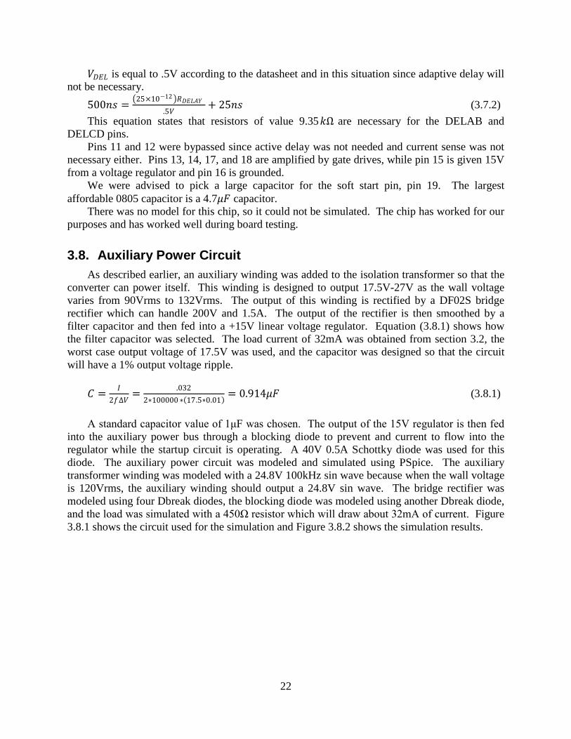
Figure 3.9.2: PSpice simulation results of rectification part of +/-15V output circuit.
Figure 3.9.3: PSpice simulation results of filtering and voltage regulation of +/-15V output
circuit.
4. PCB LAYOUT Layout of the PCB was very interesting. The team divided the power supply into functional
groups much like Section 3 of this report. With these divisions the team cut out little areas with the functional groups written down on pieces of paper. These pieces of paper were placed into areas while considering noise and functionality. Outputs should be placed on the edge of the board, and not landlocked by delicate components. Traces should be as short as possible to decrease noise. Four-layer board design was chosen to take advantage of power and ground

26
planes. Test points were added in late in the design and created difficulty in avoiding flooded power and ground planes. The layout can be seen in Appendix II.
5. BOARD TESTING AND REVISIONS
5.1. Initial Problems After receiving the PCB board and began to populating the components, we realized that we
had made several layout mistakes. First of all, the hole sizes for two of the components (R1 and L1) were much too small. To solve this, R1 was soldered directly to the pins of the components that it lies between (U1 and C1). For L1, we scraped an area of photoresist off of the traces and soldered the inductor leads directly to the traces. Next, we realized that the two of the pins for U1 (the initial bridge rectifier) were mixed up. Fortunately this is a through-hole component so it was easy to twist and tape the two leads that were mixed up. Also, we had problems with the start-up circuit. It wasn’t turning on at first, but we decreased the value of the power resistor R1 from 3.6K to 1.8K and then it started working. Three more problems we ran into were with the gate drive transformers, leakage inductance, and isolation transformer which are discussed in the following three sections.
5.2. Gate Drive Transformers The surface mount gate drive transformers that we chose turned out to have a V*μs that was
much too low so they were saturating and acting like a short circuit. Therefore we had to design our own gate drive transformers using a toroidal ferrite core. The core we selected had cross sectional measurements of 4.2mm x 4.5mm. Using equation (5.2.1) we calculated the number of turns for the primary side.
𝑁𝑁 = 𝐷𝐷𝑉𝑉
2∗𝐵𝐵𝑟𝑟𝑚𝑚𝑚𝑚 ∗𝐴𝐴𝑐𝑐∗𝑓𝑓𝑟𝑟= 0.5 ∗ 15𝑉𝑉
2∗0.25𝑇𝑇∗4.2𝑟𝑟𝑟𝑟∗4.5𝑟𝑟𝑟𝑟 ∗50𝑘𝑘𝑘𝑘𝑘𝑘= 15.9 𝑐𝑐𝑐𝑐𝑟𝑟𝑚𝑚𝑟𝑟 (5.2.1)
The gate drive transformer was designed to be a 1:1:1 ratio so we chose 20 turns for each
side.
5.3. Leakage Inductance During initial testing, we weren’t able to output more than 30W due to losses in the leakage
inductor because the inductance was too high. We build a new inductor that is 26μH instead of the originally designed 498μH and then the circuit began to work much better. The measured leakage inductance of the primary side of the isolation transformer was 22μH so the total leakage inductance is 48μH. Equations (5.3.1) and (5.3.2) show that zero voltage switching should now start occurring at 75.78W.
12𝐿𝐿𝐼𝐼2 > 1
2𝐶𝐶𝑉𝑉2 → 𝐼𝐼 = 𝐶𝐶𝑉𝑉2
𝐿𝐿 445.74𝑟𝑟𝐴𝐴 (5.3.1)
𝑃𝑃 = 𝑉𝑉𝐼𝐼 = 170 ∗ 301.38𝑟𝑟𝐴𝐴 = 75.78𝑊𝑊 (5.3.2)

27
5.4. Isolation Transformer Even after the smaller leakage inductor was implemented, the 120Hz input voltage ripple
was still appearing on the output voltage waveform at power levels above 150W which can be seen in Figure 5.4.1. This waveform was taken with a 250W output. This ripple was showing up because the converter was operating at maximum duty cycle, so when the input voltage dropped the convert couldn’t increase the duty cycle to increase the output voltage. The transformer waveforms can be seen in Figure 5.4.2. Since the converter’s duty cycle was maxed out at 150W output with a 120Vac input, we decided to redesign the isolation transformer to have a much lower turns ratio so that the converter would be operating at much lower duty cycle.
Figure 5.4.1: 120Hz input voltage ripple showing up on output voltage waveform at 250W.

28
Figure 5.4.2: Transformer waveform of converter operating at 250W. Here it can be seen
that the system is operating at maximum duty cycle.
The current transformer turns ration was 2:1 with the primary side windings being 48 and the secondary being 24. We lowered the turns ration to 1.36:1 by changing the primary side to 45 and the secondary to 33 windings. We were able to leave all of the 15V secondary windings at 7 windings each.
5.4.1. Buck Converter Power Stage Revisions Since the transformer design changed to 1.36:1 turns, the output inductor had to increase
in value. The duty cycle decreased and resulted in the following inductance calculation. 𝐿𝐿 = 𝐷𝐷′ 𝑉𝑉𝑜𝑜
2𝑓𝑓𝑟𝑟Δ𝑚𝑚𝐿𝐿 (5.4.1.1)
𝐿𝐿 = (1−72/125)×72𝑉𝑉2(100𝑘𝑘𝑘𝑘𝑘𝑘 ).7𝐴𝐴
𝐿𝐿 = 218𝜇𝜇𝑘𝑘
To further decrease voltage ripple, the output capacitor was increased to 20𝜇𝜇𝜇𝜇. This decreased the output ripple below 0.5V.

29
5.4.2. Feedback Loop Revisions Now that a new output filter was designed, it was necessary to redesign the compensator.
Using the same design procedures as discussed in section 3.5, a new compensator was designed. The resulting component values are shown in Table 5.4.1.
Table 5.4.1: Compensator Component Values
Component Value Rbias 2.94kΩ
R1 82.5kΩ R2 82.5Ω R3 39.2kΩ C1 15nF C2 10pF C3 3.3nF
5.4.3. Transformer Waveforms The leakage inductor of the transformer was not sufficient enough to provide soft-switching.
Therefore a series inductor was added before the primary winding of the transformer. This series inductor caused losses in the duty cycle which can be shown in Figure 5.4.3.2. This ultimately caused the input voltage ripple to show up on the output voltage.
Figure 5.4.3.1 The primary transformer waveform can be seen without distortion, as the
secondary side waveform contains some ringing; this screenshot was captured at 20W with 50V/div and 5𝜇𝜇𝑟𝑟/div

30
Figure 5.4.3.2 The primary transformer winding can be seen without much distortion and
the secondary side contains ringing as well as duty cycle limitation as shown by the delay in output voltage; this screenshot was captured at about 200W with 50 V/div and 5𝜇𝜇𝑟𝑟/div
5.5. Input Rectification The first thing that we tested was the wall input and rectification stage for the power supply.
In the following figure, the channel 3 is the wall voltage and channel 1 is the rectified DC voltage.
Figure 5:5.1: Input rectification waveforms.

31
5.6. Controller Chip The following two figures show the ramp generator of the UCC2895 controller chip and all
four gate drive waveforms.
Figure 5.6.1: Ramp generated by the UCC2895.

32
Figure 5.6.2: Gate drive waveforms.
5.7. Output Voltage After the modifications discussed in sections 5.2 through 5.4 were made, our output voltage
was very close to 72V and had around a 0.5V ripple, as was designed for. Figure 5.7.1 shows the output voltage at 20W. At such a light load, the output voltage was a little higher than expected because the converter needs to be operating at a certain power level in order to be able to properly regulate. At 20W the output voltage was at 77.57V with a 0.51 volt output voltage ripple. Around 40W the output voltage became a constant 72V. Figure 5.7.2 shows the output voltage waveform at 100W. Here the output voltage level was 71.93V with a 0.45 volt ripple. Figure 5.7.3 shows the output voltage waveform at 200W. The output voltage was 71.49V with a 0.47 volt ripple.

33
Figure 5.7.1: Output voltage at 20W.
Figure 5.7.2: Output voltage at 100W.

34
Figure 5.7.3: Output voltage at 200W.
5.8. Zero Voltage Switching Zero voltage switching was achieved with the MOSFETs. This can be shown by the
following graphs. All of the gates to source voltages are 20V/div and all of the drain to source voltages are at 100V/div. The time scale is 500 ns/div.
Figure 5.8.1 Looking at the top pair of waveforms, the square wave is 𝑣𝑣𝐷𝐷𝑂𝑂 and the rising
waveform is 𝑣𝑣𝑔𝑔𝑟𝑟 . Drain to source voltage drops to 0V before the first MOSFET turns on; soft –switching is achieved

35
Figure 5.8.2 Looking at the bottom pair of waveforms, the square wave is 𝑣𝑣𝐷𝐷𝑂𝑂 and the rising
waveform is 𝑣𝑣𝑔𝑔𝑟𝑟 . Drain to source voltage drops to 0V before the second MOSFET turns on; soft –switching is achieved
Figure 5.8.3 Looking at the top pair of waveforms, the square wave is 𝑣𝑣𝐷𝐷𝑂𝑂 and the rising
waveform is 𝑣𝑣𝑔𝑔𝑟𝑟 . Drain to source voltage drops to 0V before the third MOSFET turns on; soft –switching is achieved

36
Figure 5.8.4 Looking at the bottom pair of waveforms, the square wave is 𝑣𝑣𝐷𝐷𝑂𝑂 and the rising
waveform is 𝑣𝑣𝑔𝑔𝑟𝑟 . Drain to source voltage drops to 0V before the fourth MOSFET turns on; soft –switching is achieved
6. SUMMARY AND CONCLUSIONS We successfully designed a 200W power supply at 72V. However there were a few
modifications that needed to be made in order to get the original design to work properly. These modifications were made over the course of the semester and now our power supply is successfully working according to specification.
Much was learned about power supply design. Achieving zero voltage switching is no easy task and must be planned carefully. This was discovered by the appearance of 120Hz ripple on the output waveform. This ripple emerged due to duty cycle limitation caused by a high inductance on the leakage inductor on the primary side of the transformer. This large inductance was required to achieve zero voltage switching, by resonating with the capacitance of the MOSFETs. So the team experimented with power MOSFETs with much less capacitance. However, due to this smaller capacitance zero voltage switching was harder to achieve since gate drive resistors would have to be chosen more carefully; a change in resistance would affect the rise and fall time of 𝑣𝑣𝐷𝐷𝑂𝑂 more in MOSFETs with less capacitance. The team was limited in choice of resistors at the time, so the experimental MOSFETs were not used. Finally, compensator design should have been simulated at light load and full load, so change in power would not adversely affect performance. This would explain the higher voltage at light load.
7. TI PARTS USED FOR DESIGN The UCC2895 was the brain of the power supply. A switch mode power supply cannot
operate well without accurate timing control and feedback. These qualities are met by the

37
UCC2895. The UCC2895 is a phase shift modulated control chip which allowed us to achieve zero voltage switching. This eliminated most switching losses and noise.
The four outputs need to be amplified in order to drive power MOSFETs with little delay. The TPS2812 gate drivers fulfill this need. The rise and fall times of the amplified signals are equivalent which is also integral to the implementation of a full bridge buck converter.
The TL431B shunt regulator made the design of the feedback loop very easy. It was used to design a compensator in conjunction with an optocoupler to provide complete feedback isolation from the secondary and primary sides of the converter.
Voltage regulators are great power devices for analog chips. The UA7815 was used to provide power to the Class D amplifier’s chips. This chip also provides regulation in a small footprint as opposed to alternative components, like Zener diodes and resistors. Its power efficiency is also greater than a group of components.

38
PART II: CLASS D AMPLIFIER
1. INTRODUCTION A block diagram of the amplifier and subwoofer system is shown below in Figure 1. All
Class-D amplifiers operate through the generation of a pulse width modulation signal from the comparison of a triangle wave to the audio signal. This PWM signal is then fed to gate driving circuitry that provides the necessary gate charge to switch the output devices, generally MOSFETs, on and off. The amplified signal from the output devices is then passed through a low-pass filter to recover the amplified audio signal. Unique to our project, an accelerometer mounted on the cone of the woofer provides a feedback signal which is conditioned and fed back to the input of the amplifier.
Figure 1: Block diagram showing the components of the Class-D amplifier and active feedback system.
2. INPUT STAGE DESIGN
2.1. Triangle Wave Generator Design In order to create a proper PWM signal from an audio input we first needed to develop a
triangle wave generator that was very stable and met the required specifications. A triangle wave was chosen over a ramp generator to alleviate the need to level shift the input signal. In defining our requirements we determined that we wanted a switching frequency that was high enough that the lower harmonics could easily be attenuated by a low pass filter and that the amplitude was large enough to properly modulate an audio signal from most sources.

39
The switching frequency we chose was 100 kHz which limited the amount of harmonics at our target listening frequencies. The amplitude was chosen at 3 Vp since the average audio input signal is roughly 1.5 – 2 Vp. With these parameters defined we went with a simple yet stable triangle generator design that is show in Figure 3.
Figure 2: Triangle Wave Generator
The design above is a Schmitt trigger with an integrator to develop the triangle wave. The
op amp U1 is used as the integrator and the current drive for C1, we chose the TI OPA228 series op amp to be this IC due to its high GBP and also because it is rated for audio applications. U2 is a comparator configured as a Schmitt trigger and has the speed required for our switching frequency. A desirable feature of this design is that the frequency of the waveform is controlled completely by external components. The output frequency is calculated by the following equation:
𝑓𝑓𝑜𝑜 =𝑅𝑅3/𝑅𝑅2 4𝐶𝐶1𝑅𝑅1
(2.1.1)
After calculating the values we modeled the circuit in PSpice. As you can see in the
simulation results our waveform is a stable triangle wave that achieves the specifications outlined above.
0 0
U2
LM111
OUT 7 + 2
- 3 G 1
V+ 8
V- 4
B/S 6 B 5
R4 1.8k
VCC
R5 681
Tri-wave
V
U1
OPA228 3 +
7 +Vin
4 -Vin 6
2 - R1 500 R2
10k
R3 10k
C1 5n VCC
VCC
VEE
VEE

40
Figure 3: PSpice Simulation Output of Triangle Wave Generator
2.2. Volume Control Design For the input stage we wanted to incorporate a volume control, a low pass filter, and a
compensator. The volume control served two purposes when originally conceived. The first purpose was to provide gain, should we need it, from a low level signal. The second purpose was to provide non linear control of this gain. Human hearing is non linear in nature, such that, if we were to implement a simple gain circuit the output we would hear would not sound correct. The volume control circuit below solves this problem as well as provides a sufficient amount of gain.
Figure 4: Volume Control Circuit
This circuit was designed by Elliot Sound Products for free use and solved the problems we
needed to address. VR1 is a variable resistor that sets the gain for the circuit. The magnitude of VR1 also sets the input impedance of the circuit itself so it’s easily customizable to any situation. The first half of the TI TL072 was used as an input buffer while the second half was used for gain.
Time
0s 4us 8us 12us 16us 20us 24us 28u
32u
36u
40us V(Tri-wave)
-4.0V
-2.0V
0V
2.0V
4.0V Fo= 100
Vp =

41
2.3. Input Filter Design The next part of the input stage we designed was the input filter. This amplifier is used for
subwoofer driving and as such is only concerned with low frequencies. The cutoff frequency is entirely up to the user’s preference, so for sound quality purposes we chose to have a cutoff frequency of 150 Hz. To simplify the process of designing the input filter we used FilterPro v2.0 from Texas Instruments. This program enabled us to quickly draft a filter to meet our needs.
Figure 5: FilterPro v2.0
As mentioned previously we wanted to design the filter for 150 Hz, but we also wanted it to provide plenty of attenuation for any switching frequency harmonics that might present themselves in the signal. To provide for this requirement we choose to go with a 2nd order Sallen-key Butterworth Low Pass filter. Inputting these specifications yielded the circuit below:
Figure 6: Low Pass Input Filter
Using PSpice to do a frequency sweep of the circuit yielded the following results that meet
the graphs given by FilterPro and our specifications.
C4
390n
C582n
0
Audio In
FREQ = 80VAMPL = 1VOFF = 0
U7
OPA228
3+
7+V
in4-V
in
6
2-
VEE
VCC
R6
2.21k
R7
15.8k

42
Figure 7: Low Pass Filter Frequency Sweep Results
2.4. Compensator Design In applying feedback it is necessary to compensate that feedback before applying it back to
the circuit. We chose to use a PID controller to compensate our feedback. We initially wanted to have three settings on the amplifier so that we could show the difference in output between open loop, closing the loop from the output filter, and closing the loop from the accelerometer feedback. As time narrowed we decided to only have open loop and closed loop from the accelerometer.
Closing the loop from the accelerometer was more of a challenge to model than we
originally had planned. While trying to model the feedback we determined that we needed to do real test with the accelerometer before we could design the components for the PID controller. We then decided to only leave pads on the board to be designed later after real tests could be completed. We also designed a header that acted as a jumper such that we could change between the two modes of operation.
3. OUTPUT STAGE DESIGN
3.1. Gate Driving An Intersil HIP4080A was chosen to perform the gate-driving of the four output MOSFETs.
This component was chosen because it provides a single solution for both high and low side driving of a full-bridge output configuration. This circuit uses a bootstrapped gate driving topology to provide the gate driving signal for the high-side MOSFETs. In bootstrapped gate
Frequency 1.0Hz 3.0Hz 10Hz 30Hz 100Hz 300Hz 1KHz 3KHz 10KHz 30KHz 100KHz 300KHz 1MHz
DB(V(U7:6))
-100
-80
-60
-40
-20
0 -3dB @ Fc = 150
20

43
driving, the gate driving circuit uses a diode to charge a capacitor using the upper supply rail of the MOSFET and the low-voltage supply of the circuit. The circuit then discharges the capacitor into the gate of the MOSFET to switch it on. The HIP4080A also includes an internal comparator which allows internal generation of a PWM signal from the input audio signal and triangle wave as well as selectable dead time adjustment for both sides of the full bridge.
International Rectifier IRFB4212 MOSFETs were chosen for this project because of their
specialized design for Class-D amplifiers. These MOSFETs have a low Rds (75 mOhm) which minimizes conduction losses as well as a low gate charge (15 nC) which allows faster switching and minimal switching losses. Furthermore, the reverse recovery charge of the body diode in these MOSFETs has been minimized to reduce their effect on the amplifier’s total harmonic distortion. The complete implementation is shown in Figure 8.
Figure 8: Output stage configuration showing bootstrapped gate-driving circuitry.
Turn-on and turn-off resistors were employed to switch the MOSFETs on and off at rates
that would minimize losses, ringing, and prevent damage to the HIP4080A driving circuitry. A 1N4148 diode acts as a switch for the upper resistor such that the MOSFET is only charged through the bottom resistor yet discharges through the parallel combination of both resistors. The turn-on resistance was determined using the method defined in the ECE 4206 gate driving notes and the calculation is shown below:
(3.1.1)
It would be ideal to turn of the MOSFET as fast as possible in order to limit conduction losses as well as the possibility of “shoot-through” currents which occur when both the high and low side MOSFETs are turned on. However, the HIP4080A is limited in the amount of current that it can sink. In order to prevent damage to the driving circuitry the turn-off resistance was calculated using 2.1 amps as the maximum current the HIP4080A could sink. The calculations for turn-off resistance are shown below including proper sizing of the resistance through its parallel combination with RON.
Ω→=== 184.17)515(
)11)(35)(12(22 pF
pFnHC
gCLR
GS
fsGDDSON

44
(3.1.2)
Selection of the bootstrap driving components (diode and capacitor) is fairly straightforward. The capacitor must be sized to provide adequate charge to the MOSFET gate in order to keep the device turned on for the duration of its switching cycle. A high-quality dielectric is also preferable to minimize losses in the capacitor itself. For this project a .1uF NPO/COG capacitor was used as the bootstrap capacitor. The bootstrap diode must be chosen to minimize reverse recovery charge which may prevent the gate of the MOSFET from being fully switched on. We employed Fairchild ES1D ultrafast rectifier diodes with a reverse recovery time of 15 nS and a reverse recovery current of 5 uA, resulting in a reverse recovery charge of 3.75e-14 C. In relation to the size of our bootstrap capacitor, the reverse recovery losses in the bootstrap diode are negligible.
Finally, the HIP4080A dead time resistances HDEL and LDEL were set using the
application note from Intersil. The largest recommended dead time of 120 nS (250 kOhm) was selected in order to minimize the possibility for shoot through currents. This decision was made to ensure safe operation of the output MOSFETs and comes at the price of increased harmonic distortion.
3.2. Output Filter Design A low-pass filter is required to recover the amplified audio signal from the output pulse-
width-modulated signal. Furthermore, this filter will mitigate the radiation of electromagnetic interference from the speaker leads. The cut-off frequency of this filter is determined by the desired level of attenuation of the switching frequency and the bandwidth of the audio signal to be output. These requirements introduce a tradeoff between adequate suppression of switching noise, component size and cost, as well as maintaining audio fidelity. Because our amplifier was meant for a subwoofer, the bandwidth of the output audio signal was sufficiently low, thus our constraint on cut-off frequency was mainly component size and cost. A cut-off frequency of 10 kHz was chosen in order to provide approximately 1 decade of attenuation (40dB) of the switching frequency while not requiring overly large inductors or capacitors. A common-mode topology was chosen as shown below in Figure 9, and component values were calculated using the following equations.
(3.2.1)
Ω=→+
=+
====−
1118187
1.215
OFFOFF
OFF
OFFON
OFFON
PeakG
GOFF R
RR
RRRR
AV
IVR
TTC LC
fπ2
1=
221TLLL == TCCC 221 ==

45
Figure 9: Common-mode output filter configuration for the suppression of the switching frequency.
For simplicity, the speaker was modeled as an 8 ohm resistance in the design of this filter
however in reality this is not an accurate model of the speaker. Shown in Figure 10 is the ideal response of the output filter and the real response of the output filter. As can be seen in the frequency response graph, the rising impedance of a speaker causes a spike in response at the resonant frequency of the filter. In some situations this may cause both audio fidelity and amplifier stability to suffer. However, in our case this spike was beyond our desired bandwidth and would not cause any negative effects to our amplifier’s performance. Compensation for this resonant spike requires the addition of another pole-zero combination in the output filter which would require additional components for negligible benefit.
Figure 10: Frequency response of the output filter with an ideal 8 ohm load and an inductive load.
Ideal
Actual

46
3.3. Accelerometer Feedback In order to provide a reduction in distortion from the subwoofer system, an accelerometer
was to be mounted to the cone of the speaker to provide motional feedback to the input of the amplifier. This system of negative feedback should both reduce the harmonic distortion of the speaker while at the same time allow the frequency response and quality factor “Q” of the system to be user selected. The first step in design of a compensation scheme for the amplifier was to adequately characterize the transfer function of the system. This required the derivation of transfer functions in the Laplace domain to describe the acoustic output of the system and the motion of the speaker cone in a closed box.
To start, the subwoofer’s Thiele/Small parameters were measured using a Dayton Woofer Tester II loudspeaker measurement system. Thiele/Small parameters are a set of values which describe the electro-mechanical properties of a speaker and predict its performance in a certain enclosure. The prediction of the acoustic output of a sealed-box loudspeaker is analogous to a 2nd-order high-pass filter. In the case of the loudspeaker system, the resonant frequency and Q of the roll-off is a function of the loudspeaker parameters and the size of the enclosure in which it is installed. The values were measured by the Dayton Woofer Tester II system and were inserted into the standard 2nd-order high-pass transfer function as shown in the equations below: (3.3.1) (3.3.2)
With the derivation of this transfer function complete, predicting the acoustic output of the loudspeaker system was completed using an “analog behavioral model” in PSpice. Figure 12 below shows the predicted output of the JL Audio 12W1v2-8 subwoofer in a 1.25 cubic foot enclosure. From the frequency response graph it can be seen that the -3dB point of the system is approximately 41 Hz and the Q of the system (.8419) causes a slight “hump” in magnitude response above of the resonant frequency of 47.9 Hz.
Figure 11: Analog behavior model and predicted frequency response of the closed-box subwoofer.
HzQ
fQfTS
STCC
9197.47=×
=
( ) ( )22
2
22
2
)9197.47(28419.
9197.47222)(
ππππ +
+
=+
+
=ss
s
fsQfs
ssH
CTC
C

47
Determination of the resonant frequency and quality factor of the closed-box loudspeaker system also allows for the derivation of a transfer function of the motion of the cone. Cone displacement in the frequency domain is analogous to a 2nd-order low-pass filter because an increase in cone-excursion is required to maintain the same sound level at lower frequencies. The measured resonant frequency and quality factor can be inserted into the standard 2nd-order low-pass transfer function to accurately predict the motion of the loudspeaker cone.
(3.3.3)
Difficulty in describing the speaker cone displacement arises when one tries to determine
the scaling factor H(0). For this analysis, it was assumed that speaker cone displacement would increase linearly with an increase of input power. Therefore to determine the scaling factor H(0) we need to determine the cone excursion for a given input power level and use this data point to determine the cone excursion at our reference level (0dB). This analysis was performed by determining the input power required to drive the cone to its excursion limits. Using the method described in “The Loudspeaker Design Cookbook” by Vance Dickason, maximum electrical input power can be found by dividing the maximum acoustic output power by the efficiency of the system which is determined by the measured Thiele/Small parameters as shown below.
0ηAL
ELPP = where 002634.))(1064.9( 310
0 =×
=−
ES
ASS
QVfη
(3.3.4)
Maximum acoustic output power is a function of the -3dB point of the loudspeaker system and the volume of air that the subwoofer is capable of displacing. In our case, the JL Audio 12W1v2-8 subwoofer has a radiating area of .0525 m2 and a maximum excursion of 9.5 mm.
WVfP dAL 479587.))()(653.0( 243 ==
(3.3.5)
From these two calculations the amount of electrical power required to produce 9.5 mm of excursion is:
mmVWPP ALEL 5.91655.38076.182
0
=→==η
(3.3.6)
Therefore the amount of excursion produced at our reference level of 0 dBV is:
mmV 249.1 →
With the H(0) scaling factor now calculated, another analog behavioral model can be used to
determine the cone excursion of the subwoofer at a given frequency and power level. The results of this simulation are shown in Figure 12. Because PSpice analog behavioral models automatically output a voltage it is necessary to specify that in the plot 1V equals 1 meter of excursion. Figure 12 shows the predicted cone excursion of our subwoofer with 182 Watts of input power. As we can see in the graph, the input power results in 9.5 mm of excursion.
22
2
)2(2
)2()0()(
CTC
C
C
fsQfs
fHsHππ
π
+
+
=

48
Figure 12: Excursion versus Frequency
Because acceleration is the second derivative of position, the output of the accelerometer in the Laplace domain can be determined by multiplying the transfer function of cone excursion by s2. A Freescale MMA1212EG accelerometer was chosen because of its fairly low-cost and ability to measure high-G forces (>150 G). This accelerometer has a gain of 10mV/g and so its output voltage in the Laplace domain can be calculated using the following equation:
(3.3.7)
At full input power, the expected output of the accelerometer is shown in Figure 13.
Figure 13: Anticipated accelerometer output from the subwoofer at full power.
The two zeros introduced by the accelerometer in the feedback loop compensates for the
falling response of the subwoofer at lower frequencies. Thus, the -3dB point of the system is no-longer determined by the interaction of the subwoofer and its enclosure. Instead, we can use the loop-gain in the feedback path to determine the new 3 dB point of the system. For our project, by
gmV
smgssHA EOUT
10*)/(8.9
)(1**)( 22=

49
adding a gain of 6 after the accelerometer, our -3dB point is reduced to 30 Hz before the subwoofer runs out of excursion capabilities. In order to prevent the speaker system from playing low frequencies at a power level that would be damaging to the woofer, a 2nd-order high-pass filter is added to the input. The order and quality factor of this filter now determines the acoustic response of the system. The final system is shown in Figure 14.
Figure 14: Block diagram of the amplifier, subwoofer, and accelerometer feedback system.
For this project, a high-pass filter with a corner frequency of 30 Hz and a Q of .707 was
chosen to allow maximally flat (Butterworth) response in the system’s passband and to prevent frequencies below the -3dB point set by the loop-gain from being played. The new acoustic response of the system is shown in Figure 15. As can be seen in the figure, the new -3dB point is 10 Hz below the original -3dB point and the .707 alignment eliminates the previous ripple in the system’s passband. This compensation comes at the price of reduced output of the system.
Figure 15: Frequency response graph of the accelerometer-compensated system.
4. PCB LAYOUT The PCB layout was accomplished through the use of the program Protel DXP. There were
several concerns that we wished to address in implementing in the PCB layout. Among our concerns were sectioning the board appropriately, using proper signal pathing, and the gate drive section.
Compensated
Original Response

50
We separated the input and output sections such that they would not cross. The lower left hand side of the board was used to place all of the input section. The components were aligned neatly and no excess runs of traces were used. The signal path was kept as short as possible and avoided crossing the power planes whenever necessary to avoid noise injection.
The gate driving section was the main cause for concern. The gate drive paths were kept extremely short to minimize miller effect. The source return paths ran directly underneath the gate drive paths to minimize inductance.
All bypass capacitors were mounted as close as possible to power and ground. The larger components were mounted near the edges of the board for ease of access. The MOSFETs were also mounted near the edge of the board such that a heat sink could easily be applied.
The PCB board was a four layer board. Each layer can be viewed in Appendix II.
5. SUBWOOFER ENCLOSURE DESIGN In order for the subwoofer to perform as expect an enclosure needed to be built. We
followed the specifications outlined by JL Audio in the subwoofers datasheet. The internal volume of the enclosure was 1.25 cu. For cosmetic appearances we added a wood grain finish and black carpeting to the outside of the box as well as a terminal cup for ease of use.
6. INPUT STAGE IMPLEMENTATION Having all sections design and the PCB board made we next turned to implementation and
testing. We were first off completely surprised that right away we had no output what so ever. The triangle wave was tested individually and resulted in producing nothing. After further testing we realized that no power was being applied to the +15V power plane that the triangle wave generator rested on. We came to the conclusion that this was an oversight by the manufacturer as it is connected in our schematic that was sent to them. We used a jumper from another location to apply power to this plane and immediately started to see output.
We were next surprised to see distortion in our audio signal. There was cross over distortion in the signal and as such reflected in the PWM output. The PWM output seemed to only be active during the positive half of the waveform cycle. This led us to determine a huge oversight. The HIP4080A was a single supply chip. This meant that the triangle wave and the audio input needed to be level shifted.
To solve this problem we removed the volume control circuit as it wasn’t necessary for the amplifier to work and developed a level shifting circuit in its place for the audio input. The triangle wave was level shifted similarly.
After level shifting these signals the PWM output was text book. The triangle waveform in testing was 91 kHz. This falls short of the 100 kHz we wanted to achieve but it is close enough for our purposes. The amplitude of the triangle wave was within specification.
The figure below shows the three signals from their test points. The audio signal in is much higher frequency than we will use in practicality but to show all three waveforms it was necessary to increase the frequency.

51
Figure 16: Input Stage Outputs
7. OUTPUT STAGE IMPLEMENTATION Upon first testing the output of the amplifier we were pleased to see it working properly.
The MOSFETs ran cool at 25o C even without a heat sink. Figure 17 displays an output waveform at fairly low power levels, switching noise is noticeably absent from the output signal illustrating the output filter’s adequate attenuation level.
Figure 17: Output waveform (bottom) at low-power showing adequate reduction in switching noise.
With the output working properly we checked the gate drive waveforms next. A sample
gate drive waveform is shown in Figure 18. From the oscilloscope display we can see that the capacitor is properly sized because there is no drop in voltage at that gate during the switching

52
cycle. Also, the waveform is devoid of significant ringing and overshoot indicating that the PCB layout minimizes induction and the Miller effect in the MOSFETs.
Figure 18: Gate driving waveforms for the low-side MOSFETs under load.
We were excited to check the dead time as a final check to our design. With the cleanliness of the output we expected it to be minimal. The dead time of each half-bridge is shown in Figure 19. Dead time ranged from 80 nS to 130 nS depending on the output power of the amplifier. Also, notable in the picture is the difference in dead time between each half-bridge. The cause of this phenomenon has not yet been determined but it is pronounced enough to rule out minute differences in the HDEL and LDEL resistors as the cause.
Figure 19: Gate driving waveform of the high-side (upper) and low-side (lower) MOSFETs. The waveforms have been
magnified to show asymmetric dead time.
During the testing of the output stage we managed to blow one MOSFET. We had been
playing the system for around two hours before the MOSFET died. We were unable to
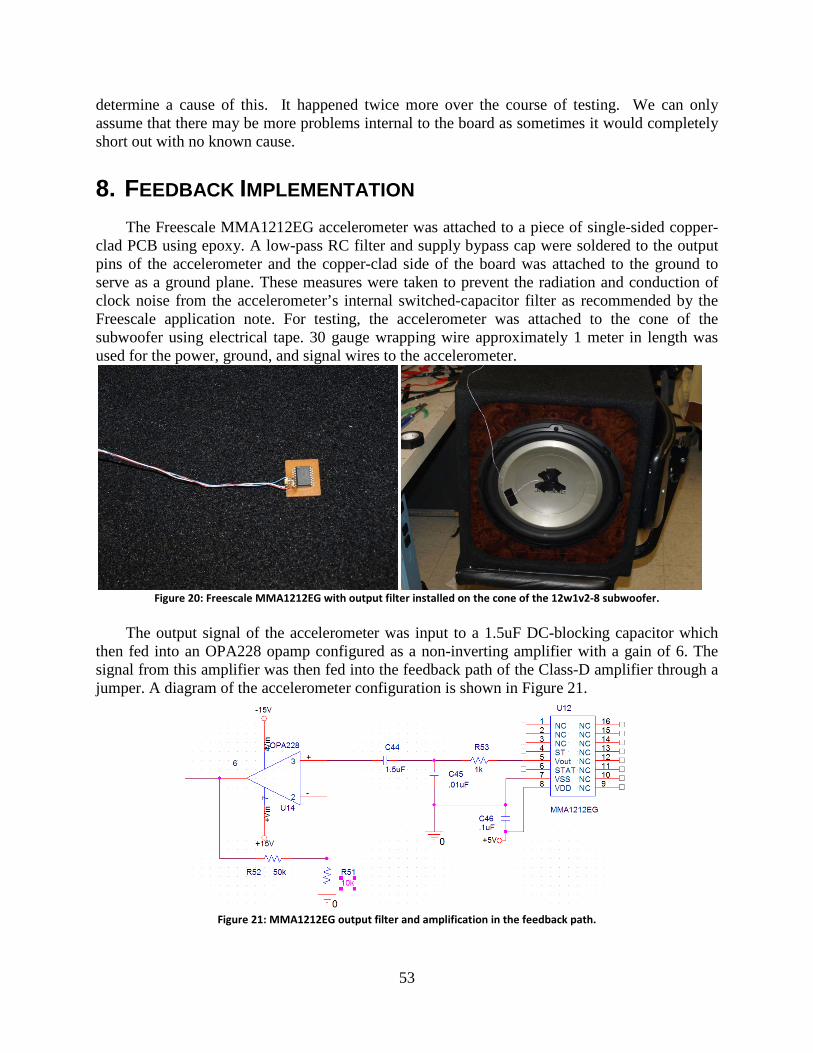
53
determine a cause of this. It happened twice more over the course of testing. We can only assume that there may be more problems internal to the board as sometimes it would completely short out with no known cause.
8. FEEDBACK IMPLEMENTATION The Freescale MMA1212EG accelerometer was attached to a piece of single-sided copper-
clad PCB using epoxy. A low-pass RC filter and supply bypass cap were soldered to the output pins of the accelerometer and the copper-clad side of the board was attached to the ground to serve as a ground plane. These measures were taken to prevent the radiation and conduction of clock noise from the accelerometer’s internal switched-capacitor filter as recommended by the Freescale application note. For testing, the accelerometer was attached to the cone of the subwoofer using electrical tape. 30 gauge wrapping wire approximately 1 meter in length was used for the power, ground, and signal wires to the accelerometer.
Figure 20: Freescale MMA1212EG with output filter installed on the cone of the 12w1v2-8 subwoofer.
The output signal of the accelerometer was input to a 1.5uF DC-blocking capacitor which
then fed into an OPA228 opamp configured as a non-inverting amplifier with a gain of 6. The signal from this amplifier was then fed into the feedback path of the Class-D amplifier through a jumper. A diagram of the accelerometer configuration is shown in Figure 21.
Figure 21: MMA1212EG output filter and amplification in the feedback path.

54
8.1. Feedback Results The output waveform from the accelerometer is shown in Figure 22. This image was
captured from an oscilloscope with a 50 Hz signal playing through the subwoofer. Unfortunately, the signal from the oscilloscope, while visible, is heavily distorted by noise. This made retrieval of a feedback signal from the accelerometer impossible. Possible sources of this noise include the internal clock signal of the accelerometer and any radiated noise from the Class-D amplifier itself. The low-pass filter on the output pins of the accelerometer may have been ineffective at suppressing the internal clock noise because of the use of a ceramic capacitor in the filter. The equivalent series resistance and inductance of this capacitor may make it ineffective at filtering high frequencies. Also, the use of fairly long leads to connect the accelerometer to the amplifier PCB reduces the system’s immunity to radiated EMI.
Figure 22: Oscilloscope output showing distorted signal from the accelerometer.
A final problem with the implementation of the accelerometer was that the above analysis
fails to consider the state of the amplifier when the speaker is not playing any music. In this state, the feedback from the accelerometer is zero and therefore the input opamp is being run in an open loop mode. The opamp will saturate to one of its rails and force the amplifier to full duty cycle, causing a large DC current to pass through the speaker. This situation seems to indicate that it may be necessary to incorporate two feedback loops in the system, one for the amplifier, and one for the subwoofer/accelerometer combination.
9. SUMMARY AND CONCLUSION We successfully designed a Class D audio amplifier but failed to implement the active
feedback. As noted in the report there are methods we intend to use to implement the feedback and hope to successfully realize the active control. Our knowledge of circuit designing grew immensely in doing this project and we feel that future projects will come easier having finished the learning curve.

55
10. TI PARTS USED FOR DESIGN In the design of the Class D audio amplifier we incorporated three types of Texas Instrument integrated circuits (ICs). The first IC to be utilized was the TL072 unity-gain stable operational amplifier. This operational amplifier was selected for use in the input stage of our design due to its favorable characteristics. The TL072 is a JFET-input op amp and as such boasts high input impedance. Furthermore, The TL072 is ideal for our high fidelity needs because it is capable of a very fast slew rate (13 V/µs), low harmonic distortion, and operation with minimal noise (𝑉𝑉𝑚𝑚 = 18𝑚𝑚𝑉𝑉
√𝑘𝑘𝑘𝑘). The TL072 allowed for an excellent preamp buffer and volume
control circuit design. We followed the input stage with a low pass filter, where, in order to maintain desirable
fidelity we employed the OPA228 series of operational amplifiers. This op amp has the noted application of being used in professional audio equipment making it ideal for our design. The OPA228 series of op amps have low noise and are remarked for their precision, something very desirable in the filer we wished to incorporate. The OPA228 operational amplifier was also employed in the accelerometer feedback circuit which required low-noise and a high measure of precise gain selection. Another convenient feature of this op amp was the availability of a SPICE model, which allowed us to simulate our designs. Along with this op amp we used the filter designer FilterPro v2.0 which was available at Texas Instruments website to design the low-pass filter on the input to the amplifier.
The last Texas Instruments IC we incorporated was the LM111 comparator. Along with an OPA228, the LM111 allowed us to develop a very stable triangle wave generator which was used for PWM generation for the Class-D amplifier. The LM111 was chosen for its high speed which allowed the creation of a triangle wave with a suitably-high frequency (100 kHz). The OPA228 was used in this section again due to its very high GBP (33 MHz). The use of these three integrated circuits allowed us to create a functional analog section for the amplifier, meeting our design goals.
CONCLUSIONS Both an amplifier and a power supply were successfully designed, but they were not able to
be implemented together without a load in parallel with the amplifier. The power supply regulated 72V DC very well at power levels over 20W, but under 20W the output voltage was very high. The no load voltage was 110V. The main switching MOSFETS for the class D amplifier were only rated at 100V so we could not let the power supply operate below 20W without operating outside the devices’ limits. The +/- 15V outputs were able to power the amplifier ICs well, but there was a problem with conducted EMI. Overall, the power supply and the Class D amplifier without feedback operated well. If we had more time to work on this project, we would have designed a better feedback compensator for the power supply so that the no load voltage would be close to 72V.

56
Appendix I: Final Schematic
Figure AI1:Power Supply input power stage, and UCC2895 schematic connects to the following two diagrams

57
Figure AI2: Power Supply gate drive, switching stage, 15V regulator for UCC2895, and voltage controlled feedback

58
Figure AI3: Power Supply isolation transformer, output stage and ±15V output

59
Figure AI4: Class D Amplifier triangle wave generator, EMI filter, input filter, volume control, and compensator

60
Figure AI5: Class D Amplifier gate drive, switching stage, output filter, and output stage

61
Appendix II: PCB Layout
Figure AII1: Top layer of power supply PCB board.

62
Figure AII2: Bottom layer of power supply PCB board.

63
Figure AII3: Internal power plane layer of power supply PCB board. The bottom left plane is the
170V DC bus, the upper left is the auxiliary power, and the bottom right is the +72V output.

64
Figure AII4: Internal ground layer of power supply PCB board. The ground on the left hand side
is the primary ground and the right hand side is the secondary ground.

65
Figure AII5: Top layer of amplifier PCB board.

66
Figure AII6: Bottom layer of amplifier PCB board.

67
Figure AII7: Internal power plane layer of amplifier PCB board.

68
Figure AII8: Internal ground plane layer of PCB board.

69
Appendix III: Bill of Materials
Reference Power Supply Bill of Materials
P/N Manufacturer Description SMD/TH Package - 6EJS1 Tyco Line Filter 6A - - - PC-0102060AC03 Adam Tech Wall Plug (IEC) 15A 6ft - - C1,C2 SLPX471M250A7P3 Cornell 470uF 220V TH - C10 FCP0805H101J-J1 Cornell 100pF Bypass Cap 50Vdc SMD 805 C11, C14, C20, C21 CC0805KRX7R9BB104 Yageo .1uF Bypass Cap 50V SMD 805 C12, C13,C3,C7 C2012Y5V1E475Z TDK 4.7uF Bypass Cap 25V SMD 805 C15 UWX1E330MCL1MB nichicon 33uF 25V SMD
C16 C0805C103K5RACTU Kemet 10nF Optocoupler Filter Cap 50V SMD 805 C4, C17, C18,C9 GRM219F51E105ZA01D GRM 1uF 25V SMD 805 C5,C6 CF042G0273JBC AVX 27nF 250V Film Cap SMD 2220 C8, C19,C22 - - Snubber Space SMD 805 Cc1 CC0805KRX7R9BB68 Yageo 0.68nF 50V SMD 805
Cc2 500R15N270KV4T Johanson Dielectrics Inc 27pF 50V SMD 805
Cc3 C0805C102K5RACTU Kemet 1nF 50V SMD 805 Co UUJ2W100MNL1MS nichicon 10uF 450V Cap SMD
CT,C23 CC0805KRX7R9BB821 Yageo 820pF 50V SMD 805 D1 BZX84C13-V-GS08 ON, Vishay, Fairchild 13/13.25V Zener Diode 300mW SMD SOT-23 D10 BZX84C5V6 ON, Vishay, Fairchild 5.6V Zener Diode 300mW SMD SOT-23 D12 SMBYT01-400 STMicroelectronics 400V Ultra Fast Recovery 1A 1.05Vf SMD SMB D2 - - 10-15 V LED TH - D3,D4 STTH30R04G STMicroelectronics 30A 400V 1.3V diode SMD D2Pak
D7, D8 STPS0540Z STMicroelectronics 40Vmax .55V 0.5A Ultra low leakage Diode SMD SOD-123
D9,D5,D6,D11 MBRS130LT3G ON Semiconductor .395V 2A 30V Schottky Diode SMD SMB F1 01020071N Littelfuse Fuse Holder TH - F1 0312003.HXP Littelfuse 3A Fuse 250V - -
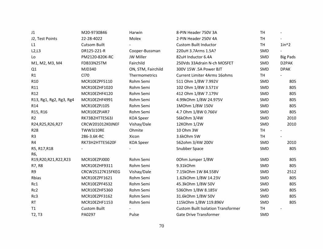
70
J1 M20-9730846 Harwin 8-PIN Header 750V 3A TH - J2, Test Points 22-28-4022 Molex 2-PIN Header 250V 4A TH - L1 Cutsom Built - Custom Built Inductor TH 1in^2 L2,L3 DR125-221-R Cooper-Bussman 220uH 3.7Arms 1.5A? SMD - Lo PM2120-820K-RC JW Miller 82uH Inductor 6.4A SMD Big Pads M1, M2, M3, M4 FDB33N25TM Fairchild 250Vds 33Adrain N-ch MOSFET SMD D2PAK Q1 MJD340 ON, STM, Fairchild 300V 15W .5A Power BJT SMD DPAK R1 Cl70 Thermometrics Current Limiter 4Arms 16ohms TH - R10 MCR10EZPF5110 Rohm Semi 511 Ohm 1/8W 7.992V SMD 805 R11 MCR10EZHF1020 Rohm Semi 102 Ohm 1/8W 3.571V SMD 805 R12 MCR10EZHF4120 Rohm Semi 412 Ohm 1/8W 7.179V SMD 805 R13, Rg1, Rg2, Rg3, Rg4 MCR10EZHF4991 Rohm Semi 4.99kOhm 1/8W 24.975V SMD 805 R14 MCR10EZPJ105 Rohm Semi 1MOhm 1/8W 150V SMD 805 R15, R16 MCR10EZPJ4R7 Rohm Semi 4.7 Ohm 1/8W 0.766V SMD 805 R2 RK73B2HTTE563J KOA Speer 56kOhm 3/4W SMD 2010 R24,R25,R26,R27 CRCW201012K0JNEF Vishay/Dale 12KOhm 1/2W SMD 2010 R28 TWW3J10RE Ohmite 10 Ohm 3W TH - R3 286-3.6K-RC Xicon 3.6kOhm 5W TH - R4 RK73H2HTTE5620F KOA Speer 562ohm 3/4W 200V SMD 2010 R5, R17,R18 - - Snubber Space SMD 805 R6, R19,R20,R21,R22,R23 MCR10EZPJ000 Rohm Semi 0Ohm Jumper 1/8W SMD 805 R7, R8 MCR10EZHF9311 Rohm Semi 9.31kOhm SMD 805 R9 CRCW25127K15FKEG Vishay/Dale 7.15kOhm 1W 84.558V SMD 2512 Rbias MCR10EZPF1621 Rohm Semi 1.62kOhm 1/8W 14.23V SMD 805 Rc1 MCR10EZPF4532 Rohm Semi 45.3kOhm 1/8W 50V SMD 805 Rc2 MCR10EZHF5360 Rohm Semi 536Ohm 1/8W 8.185V SMD 805 Rc3 MCR10EZPF3162 Rohm Semi 31.6kOhm 1/8W 50V SMD 805 RT MCR10EZHF1153 Rohm Semi 115kOhm 1/8W 119.896V SMD 805 T1 Custom Built - Custom Built Isolation Transformer TH - T2, T3 PA0297 Pulse Gate Drive Transformer SMD

71
Test Points 68000-400HLF FCI 1-PIN Header TH -
U1 KBL04 Fairchild/Vishay 400V 4A Diode Bridge Rectifier Solder Pin
Solder Pin
U10,U11 DF02S Fairchild 1.5A 200V bridge rectifier SMD SDIP U3,U4 UA7815 TI 15V 1.5A linear regulator SMD D2PAK U5 UCC2895 TI Phase-shift PWM controller SMD SOIC-20 U6 TL431B TI Precision Shunt Regulator SMD SOIC-8 U7 4N35 Fairchild Optocoupler SMD 6-SMD U8, U2 TPS2812 TI Dual low side gate driver SMD SOIC-8 U9 MC79L15ACDG ON Semiconductor Neg 15V 0.1A linear regulator SMD SOIC-8
Reference Class D Amplifier Bill of Materials
P/N Manufacturer Description SMD/TH Package C1 490-3905-1-ND Murata Electronics North America 10uf Capacitor 10% SMD 805 C16 490-1677-1-ND Murata Electronics North America .33uF Capacitor 5% SMD 805 C22 445-1352-1-ND TDK Corporation .22uF Capacitor 10% SMD 805 C23, C26 PF4105-ND Panasonic - ECG 1uF Capacitor TH - C24, C25 PF2155-ND Panasonic - ECG 1.5uF Capacitor TH - C2-C5, C10-C15, C17-C21, C28 399-1171-1-ND Kemet 0.1uf Capacitor 5% SMD 805 C31 490-1679-1-ND Murata Electronics North America 0.39uF Capacitor 10% SMD 805 C32 478-1394-1-ND AVX Corporation 0.082uF Capacitor 10% SMD 805 C9 490-1635-1-ND Murata Electronics North America 5100pF Capacitor 5% SMD 805 D1 1N4001DICT-ND Diodes Inc 1n4001 Diode TH - D2, D3 ES1DFSCT-ND Fairchild Semiconductor ES1D Diode SMD 805
D4, D5, D6, D7 1N4148WTPMSCT-ND Micro Commercial Co 1n4148 Diode TH -
NONE KA1051S28-ND Precision Electronic Components Ltd 1Meg Ohm Pot TH - Q1, Q2, Q3, Q4 IRFB4212PBF-ND IRF IRF4212 MOSFET TH -

72
R1 P100KCCT-ND Panasonic - ECG 100k ohm 1/8w resistor SMD 805
R12 P1.80KCCT-ND Panasonic - ECG 1.8k ohm 1/8w resistor SMD 805 R13 P681CCT-ND Panasonic - ECG 681 ohm 1/8w resistor SMD 805
R15 P49.9CCT-ND Panasonic - ECG 49.9k ohm 1/8w resistor SMD 805
R17, R18 P249KCCT-ND Panasonic - ECG 249k ohm 1/8w resistor SMD 805 R2 P1.00KCCT-ND Panasonic - ECG 1k ohm 1/8w resistor SMD 805
R27, R24, R21, R30 P4.99KCCT-ND Panasonic - ECG 4.99k ohm 1/8w resistor SMD 805
R28, R22, R25, R19 P11.0CCT-ND Panasonic - ECG 11 ohm 1/8w resistor SMD 805 R29, R26, R23, R20 P18.0CCT-ND Panasonic - ECG 18 ohm 1/8w resistor SMD 805 R31, R14, R10, R3, R11 P10.0KCCT-ND Panasonic - ECG 10k ohm 1/8w resistor SMD 805
R4 P2.21KCCT-ND Panasonic - ECG 2.21k ohm 1/8w resistor SMD 805
R5 P15.8KCCT-ND Panasonic - ECG 15.8k ohm 1/8w resistor SMD 805
R9 P499CCT-ND Panasonic - ECG 499 ohm 1/8w resistor SMD 805 U1 296-1282-5-ND Texas Instruments TL072 Op amp SMD 805 U2, U3, U6 OPA2228U-ND Texas Instruments OPA228 Op amp SMD 805 U4 LM111J-8-ND Texas Instruments LM111J Comparator TH 8 pin U5 LM7805 Fairchild Optoelectronics Group 5V regulator TH 3 pin U7 HIP4080AIP-ND Intersil HIP4080A Gate Driver TH 20 pin

73
Appendix IV: Device Pictures
Figure AIV1: Top of power supply
Figure AIV2: Bottom of Power Supply

74
Figure AIV3: Top of the Class D Amplifier
Figure AIV4: Testing of the Class D Amplifier