session 10: solid state physics mosfetee.sharif.edu/~sarvari/25772/pssd009.pdf · p-channel mosfet...
TRANSCRIPT

MOSFET
Session 10: Solid State Physics
1

1. I
2.
3.
4.
5.
Outline
� A� B
� C
� D
� E
� F� G
� H
� I
� J
2

1. I
2.
3.
4.
5.
MOSCap�MOSFET
3
����
p-type Si (bulk)
SiO2 (oxide)� High k
Al (metal) ~0.1~5�� �
����
p
SiO2
������ �����n+ n+
A A’
Drift current flowing between 2 doped regions (“source” & “drain”)
is modulated by varying the voltage on the “gate” electrode.
Metal-Oxide-Semiconductor
Field-Effect Transistor:

1. I
2.
3.
4.
5.
MOSFET
4
Substrate
Gate
Source Drain
GATE LENGTH, Lg
OXIDE THICKNESS, Tox
Intel’s 32nm CMOSFETs
Desired characteristics:
• High ON current
• Low OFF current
|GATE VOLTAGE|
CU
RR
EN
T
VT

1. I
2.
3.
4.
5.
N-channel vs. P-channel
5
• For current to flow, VGS > VT
• Enhancement mode: VT > 0
• Depletion mode: VT < 0Transistor is ON when VG=0V
p-type Si
N+ poly-Si
n-type Si
P+ poly-Si
NMOS PMOS
N+ N+ P+ P+
• For current to flow, VGS < VT
• Enhancement mode: VT < 0
• Depletion mode: VT > 0Transistor is ON when VG=0V
����
��
��

1. I
2.
3.
4.
5.
CMOS Devices and Circuits
6
CIRCUIT SYMBOLS
N-channel
MOSFET
P-channel
MOSFET
GND
VDD
S
S
D
D
CMOS INVERTER CIRCUIT
VIN VOUT
VOUT
VIN0 VDD
VDD
INVERTER
LOGIC SYMBOL
• When VG = VDD , the NMOSFET is on and the PMOSFET is off.
When VG = 0, the PMOSFET is on and the NMOSFET is off.

1. I
2.
3.
4.
5.
“Pull-Down” and “Pull-Up” Devices
7
� In CMOS logic gates, NMOSFETs are used to connect the output to GND, whereas PMOSFETs are used to connect the output to VDD.
� An NMOSFET functions as a pull-down device when it is turned on (gate voltage = VDD)
� A PMOSFET functions as a pull-up device when it is turned on (gate voltage = GND)
F(A1, A2, …, AN)
PMOSFETs only
NMOSFETs only
Pull-up
network
Pull-down
network
VDD
A1
A2
AN
A1
A2
AN
input signals

1. I
2.
3.
4.
5.
CMOS NAND / NOR Gate
8
A
F
B
A B
A B F0 0 10 1 11 0 11 1 0
NANDVDD
A
F
B
A
B
VDDNOR
A B F0 0 10 1 01 0 01 1 0

1. I
2.
3.
4.
5.
Qualitative Theory of the NMOSFET
9
����
p
SiO2
������ �����n+ n+
A A’ ������ �����������
�� 0�� ! 0�� �"
The potential barrier to electron flow from the source
into the channel region is lowered by applying VGS> VT

1. I
2.
3.
4.
5.
Qualitative Theory of the NMOSFET
10
p
� �n+ n+
��# $ �"
p
� �n+ n+
��# ! �"
p
� �n+ n+
��# ! �"
�%# & 0
�%# ! 0Electrons flow from the source
to the drain by drift, when
VDS>0. (IDS > 0)
The channel potential (�'()*) varies from VS at the source
end to VD at the drain end.
��# ! �" � Inversion-layer
“channel” is formed
)0 �()*
,%�%#

1. I
2.
3.
4.
5.
Qualitative Theory of the NMOSFET
11
p
� �n+ n+
��# ! �" �%# ! ��# - �"
Electrons flow from the source
to the drain by drift, when
VDS>0. (IDS > 0)
The channel potential (�'()*) varies from VS at the source
end to VD at the drain end.
��# ! �" � Inversion-layer
“channel” is formed
,%�%#
�%#./0 ��# - �"

1. I
2.
3.
4.
5.
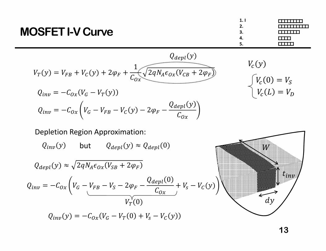
MOSFET I-V Curve
12
��
�
n+
n+
p
12)3 2
�4567)
�'()*�' 0 �#�' 1 �%
�" ��8 9 ��()* 9 2;� 9 1<=� 2>?@A=� ��8 9 2;�BCDEF()*
1. I
2.
3.
4.
5.
MOSFET I-V Curve
13
2�456
7)
�'()*�' 0 �#�' 1 �%�"()* ��8 9 ��()* 9 2;� 9 1<=� 2>?@A=� ��8 9 2;�
BCDEF()*B456 -<=� �� - �" )B456 -<=� �� - ��8 - �� ) - 2;� - BCDEF )<=�
Depletion Region Approximation:B456()* BCDEF()* & BCDEF(0*but
BCDEF()* & 2>?@A=� �#8 9 2;�B456 -<=� �� - ��8 - �# - 2;� - BCDEF 0<=� 9 �G - ��()*
B456()* -<=� �� - �" 0 9 �G - �� ) �"(0*

1. I
2.
3.
4.
5.
MOSFET I-V Curve
14
2�456
7)
�'()*�' 0 �#�' 1 �%Simply call �" 0 as �"7�' ) ,%# ∙ 7IJKL
B456()* -<=� �� - �" 0 9 �G - �� ) B456()* -<=� �� - �" 9 �G - �� ) ,%# 7)M2�456 ,%#7)(>DNN�*2�456 ,%#7)(>��456*DNN2
-B456()* < �O⁄,%#7) -DNN2B456 ) 7�'J�Q�R,%#1 DNN2 J <=� �� - �" 9 �G - �� ) 7�'�Q
�R,%# 21 DNN<=� ��# - �" - SO�%# �%#T,%#T�%#U�QR./0 0

1. I
2.
3.
4.
5.
MOSFET I-V Curve
15
,%# V21 DNN<=� ��# - �" - SO�%# �%#�%# $ �%#GWX221DNN<=� ��# - �" O�%# $ �%#GWX ��# - �"Linear
Saturation
,%
�%#
Linear Saturation
I%#
I%# T,%#T�%#U�QRYLZS
21 DNN<=� ��# - �" ZS
1. I
2.
3.
4.
5.
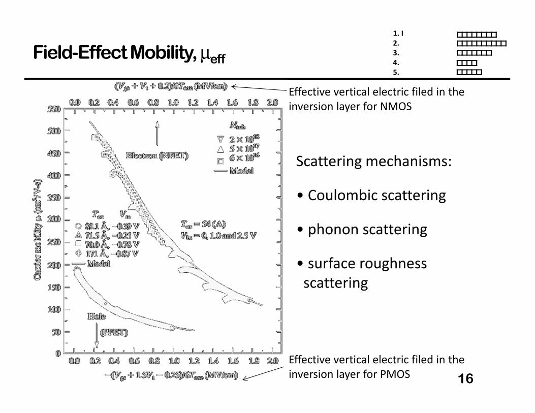
Field-Effect Mobility, µeff
16
Scattering mechanisms:
• Coulombic scattering
• phonon scattering
• surface roughness
scattering
Effective vertical electric filed in the
inversion layer for NMOS
Effective vertical electric filed in the
inversion layer for PMOS

1. I
2.
3.
4.
5.
MOSFET Saturation Region of Operation
17
p
� �n+ n+
�%# ��# - �"
�%#./0 ��# - �" p
� �n+ n+
�%# ! ��# - �"�' �� - �" �' �� - �"∆11
∆1~1,%�%#
∆1 ≪ 1As VD is increased above VG-VT, the length ∆1 of the “pinch-off” region increases. The
voltage applied across the inversion layer is
always VDsat=VGS-VT, and so the current
saturates.
If ∆1 is significant compared to L,
then IDS will increase slightly with
increasing VDS>VDsat, due to
“channel-length modulation”

1. I
2.
3.
4.
5.
“Square Law Theory” ?
18
,%# V21 DNN<=� ��# - �" - SO�%# �%#�%# $ �%#GWX221DNN<=� ��# - �" O�%# $ �%#GWX ��# - �"Linear
Saturation
Depletion Region Approximation:B456()* BCDEF()* & BCDEF(0*but
BCDEF()* & 2>?@A=� �#8 9 2;��"()* ��8 9 ��()* 9 2;� 9 1<=� 2>?@A=� ��8 9 2;�BCDEF()*B456()* -<=� �� - �" 0 9 �G - �� )
p
� �n+ n+
) BCDEF()*
�"()* ! �"(0*
�' �� - �"
BCDEF ) ! BCDEF(0* B′456 ) $ B456()* ,′%# $ ,%#

1. I
2.
3.
4.
5.
Modified (Bulk-Charge) I-V Model
19
,%
�%#
Linear Saturation
�� -�"S�� -�"
Linear
Saturation
,%# 21 DNN<=� ��# - �" - SO�%# �%#�%# $ �� - �"
Linear
,%# 21 DNN<=� ��# - �" - O�%# �%#�%# $ 1 (�� - �"*
,%# 221DNN<=� ��# - �" O�%# ! �� - �"
�%# ! 1 (�� - �"*Saturation
,%# 221DNN<=� ��# - �" O 1 9 <CDE<=� 1 9 3�=�2"Typically 1.1 $ $ 1.4
Bulk charge factor

1. I
2.
3.
4.
5.
The Body Effect
20
�" ��8 9 2;� 9 1<=� 2>?@A=� �#8 9 2;�Note that VT is a function of VSB:
�" �"L 9 1<=� 2>?@A=� �#8 9 2;� - 2;� �"L 9 a �#8 9 2;� - 2;�
a 1<=� 2>?@A=�where a is the body effect parameter
When the source-body pn junction is reverse-biased, |VT| is increased.
Usually, we want to minimize g so that IDsat will be the same for all
transistors in a circuit.

1. I
2.
3.
4.
5.
The Body Effect
21
A
F
B
A B
A B F0 0 10 1 11 0 11 1 0
NANDVDD
(∗*(�*(c* (1* �@ �%%�8 0 �(S* �%%
�"/ ! �"d

1. I
2.
3.
4.
5.
λ: Channel Length Modulation Parameter
22
p
� �n+ n+
�%# ! ��# - �",%./0 ∝ 11 - ∆1 ∆11 11 1 9 ∆11�' �� - �" �%GGWX
∆1 ∝ �%# - �%#GWX∆11 ∝ f �%# - �%#GWXf~11
,%# 221DNN<=� ��# - �" O 1 9 f �%# - �%#GWX

1. I
2.
3.
4.
5.
MOSFET: Small Signal Model
23
<gG<gC
h^ig hC9ig_
j W� ↗
�9iC_
� �� h^ 221DNN<=� ��# - �"
hC f,%GWXcut-off frequency: ⟶ h^2m<=� ∝ 11 ↘

1. I
2.
3.
4.
5.
Sub-Threshold Current
24
������>��
������ �����������
�� 0 �% 0 ������ �����������
�� ! �" �% 0
������
�����������
�� ! �" �% ! 0

1. I
2.
3.
4.
5.
Sub-Threshold Current
25
������
�����������
�� $ �" �% ! 0
,%# 21 DNN<=� - 1 op> O �q �rZ�s ^t"⁄ 1 - �Zq�QR t"⁄
<=�<CDEF�� Similarly: 1 9 <CDEF<=� 1 9 3�=�2"�8
�' �' <=�<=� 9 <CDEF ��8
ln ,%
��#�"S0
� 7 logSL ,%#7��#ZS op> ln 10 1 9 <CDEF<=�60� , NN
�ZS, NN �"O ↘ z?@ ↘⟹<CDEF ↘⟹ retrograde�=� ↘⟹ <=� ↗p ↘ (low-temperature*

1. I
2.
3.
4.
5.
P-Channel MOSFET
26
� The PMOSFET turns on when VGS < VT
� Holes flow from SOURCE to DRAIN
⇒ DRAIN is biased at a lower potential than the SOURCE
� In a CMOS technology, the PMOS & NMOS threshold voltages
are usually symmetric about 0, i.e. VTp = -VTn
P+ P+
N
GATE
VS VD
VG
ID
VB
• VDS < 0
• IDS < 0
• |IDS| increases with
• |VGS - VT|
• |VDS| (linear region)
1. I
2.
3.
4.
5.
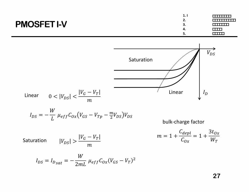
PMOSFET I-V
27
,%
�%#
Linear
Saturation
Linear
,%# -21 DNN<=� ��# - �"E - O�%# �%#0 $ �%# $ �� - �"
Saturation
,%# ,%GWX - 221DNN<=� ��# - �" O�%# ! �� - �" 1 9 <CDEF<=� 1 9 3�=�2"
bulk-charge factor

1. I
2.
3.
4.
5.
CMOS Inverter: Intuitive Perspective
28
VDD
Rn
VIN = VDD
CIRCUIT SWITCH MODELS
VDD
Rp
VIN = 0V
VOUT = 0V VOUT = VDD
Low static power consumption, since
one MOSFET is always off in steady state
VDD
VIN VOUT
S
D
G
GS
D

1. I
2.
3.
4.
5.
Voltage Transfer Characteristic
29
VIN
VOUT
VDD
VDD0
0
N: off
P: lin
N: lin
P: off
N: lin
P: sat
N: sat
P: lin
N: sat
P: sat
AAAA BBBB DDDD EEEE
CCCC
VDD
VIN VOUT
S
D
G
GS
D

1. I
2.
3.
4.
5.
CMOS Inverter Load-Line Analysis
30
VOUT=VDSn
IDn=-IDp
0
IDn=-IDp
VIN = VDD + VGSp
increasing
VIN
increasing
VIN
VIN = 0 V VIN = VDD
VDD
VOUT = VDD + VDSp
VDSp = 0VDSp = - VDD
–
VDSp=VOUT-VDD
+
0
VDD
VIN VOUT

1. I
2.
3.
4.
5.
Load-Line Analysis: Region A
31
VOUT=VDSn
IDn=-IDp
0
IDn=-IDp
VDD
–
VDSp=VOUT-VDD
+
0
VDD
VIN VOUT
VVVVININININ≤≤≤≤ VVVVTnTnTnTn

1. I
2.
3.
4.
5.
Load-Line Analysis: Region B
32
VOUT=VDSn
IDn=-IDp
0
IDn=-IDp
VDD
–
VDSp=VOUT-VDD
+
0
VDD
VIN VOUT
VVVVDDDDDDDD/2/2/2/2> > > > VVVVININININ> > > > VVVVTnTnTnTn
1. I
2.
3.
4.
5.
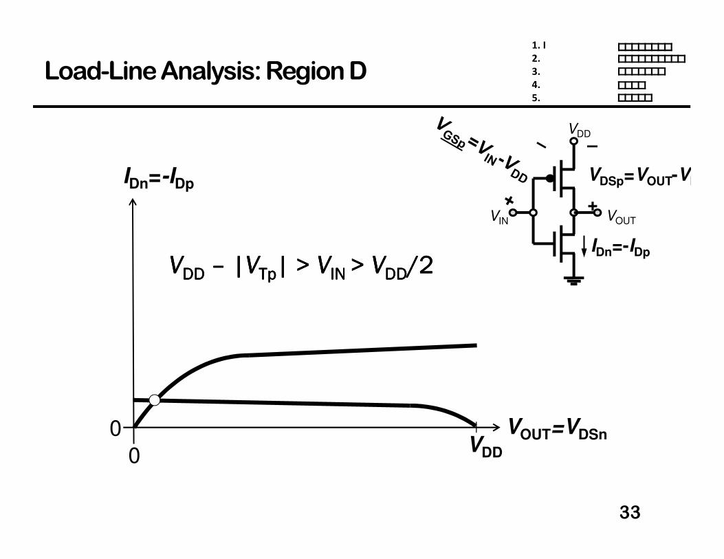
Load-Line Analysis: Region D
33
VOUT=VDSn
IDn=-IDp
0
IDn=-IDp
VDD
–
VDSp=VOUT-VDD
+
0
VDD
VIN VOUT
VVVVDDDDDDDD –––– ||||VVVVTpTpTpTp| | | | > > > > VVVVIN IN IN IN > > > > VVVVDDDDDDDD/2/2/2/2

1. I
2.
3.
4.
5.
Load-Line Analysis: Region E
34
VOUT=VDSn
IDn=-IDp
0
IDn=-IDp
VDD
–
VDSp=VOUT-VDD
+
0
VDD
VIN VOUT
VIN > VDD – |VTp|

1. I
2.
3.
4.
5.
MOSFET Scaling
35
MOSFETs have been steadily miniaturized over time
1970s: ~ 10 mm
Today: ~30 nm
Reasons:
Improved circuit operating speed
Increased device density --> lower cost per function
As MOSFET lateral dimensions (e.g. channel length L) are reduced:
•IDsat increases � decreased effective “R”•gate and junction areas decrease � decreased load “C”
� faster charging/discharging (i.e. td is decreased)
� <=� �%%,=�Intrinsic Delay

1. I
2.
3.
4.
5.
Velocity Saturation
36
Velocity saturation limits IDsat in sub-micron MOSFETS
Simple model:
108
107
106
105
102 103 104 105 106
GaAsSi
electronsholes
�(�/�*i C(�
/�* Carrier velocity vs. electric field
i V �1 9 ��GWX j��� $ �GWXiGWXj��� � �GWXiGWX �8 � 10� � �⁄ for�ZinSi6 � 10� � �⁄ for��inSi
�GWX 2iGWX
If � $ �GWX: ↦ 1 9 ��GWX

1. I
2.
3.
4.
5.
MOSFET I-V with Velocity Saturation
37
In linear region:
↦ 1 9 ��GWX,% 21 DNN<=�1 9 �%#1�GWX ��# - �" - O�%# �%# ,%K 5g��W55DF1 9 �%#1�GWX
MOSFET is Long channel if 1�GWX ≫ ��# - �"1�%GWX ��# - �" 9 11�GWX ,%
�%#
Linear
S �� - �"
Saturation
�%GWX
Long Channel
Short Channel��� 1.8�, ��3 3�,�p 0.25�,2p 45�_____µeff =200 cm2V−1s−1 ,m = 1 + 3Toxe/WT = 1.2
Esat= 2vsat / µeff = 8 ×10⁴ V/cm1 10 → �%GWX 1.3�1 1 → �%GWX 1.1�1 100� → �%GWX 0.5�1 30� → �%GWX 0.2�

1. I
2.
3.
4.
5.
IDsat with Velocity Saturation
38
In saturation region:�%# ↦ ��# - �" ,%./0 221 DNN<=�1 9 ��# - �"1�GWX ��# - �" O ,%GWXK 5g��W55DF1 9 ��# - �"1�GWXVery short channel length: 1�GWX ≪ ��# - �",%./0 22DNN�GWX<=� ��# - �" 2 iGWX<=� ��# - �"• ,%./0 is proportional to ��# - �" rather than ��# - �" O• ,%./0 is not dependent on 1 �
To improve modern MOSFETs: ,=� ↗ <=� ↗iGWX ↗high-k dielectric
strained Si

1. I
2.
3.
4.
5.
Short-vs. Long-Channel NMOSFET
39
Short-channel NMOSFET:
• IDsat is proportional to VGS-VTn rather than (VGS-VTn)2
• VDsat is lower than for long-channel MOSFET
• Channel-length modulation is apparent

1. I
2.
3.
4.
5.
Velocity Overshoot
40
When L is comparable to or less than the mean free path,
some of the electrons travel through the channel without
experiencing a single scattering event
� projectile-like motion (“ballistic transport”)

1. I
2.
3.
4.
5.
The Short Channel Effect (SCE)
41
This effect is undesirable (i.e. we want to minimize it!) because circuit
designers would like VT to be invariant with transistor dimensions and
bias condition
�% 0.125��% 4�
0.60.40.20 2 4 61(*
�"(�*“�" roll-off”
|�"|decreases with L
Effect is exacerbated by
high values of |�%#|

1. I
2.
3.
4.
5.
Qualitative Explanation of SCE
42
Before an inversion layer forms beneath the gate, the surface of the Si
underneath the gate must be depleted (to a depth 2")
�" ��8 9 2;� 9 BCDEF<=�
The source & drain pn junctions assist in depleting the Si underneath the
gate. Portions of the depletion charge in the channel region are balanced by
charge in S/D regions, rather than by charge on the gate. Less gate charge is
required to invert the semiconductor surface (i.e. |�"| decreases)
p
� �n+ n+
Depletion charge supported by S/D
Large L:
Small L:
depletion region
1

1. I
2.
3.
4.
5.
VTRoll-Off: First-Order Model
43
�" ��8 9 2;� 9 BCDEF<=�
Minimize ∆�" by
• reducing �=�• reducing ��• increasing ?@ (trade-offs: degraded DNN, )
p
� �n+ n+
1�# �" �%1′ ���� ∆�"≡ �" - �"K 5g��W55DF
∆�"∝ >?@<=� 2" 1 - 1 9 1′21 1� 1 - 2�� 1 9 22"�� - 1 → ∆�" ->?@2"<=� ��1 1 9 22"�� - 1
MOSFET vertical dimensions should be scaled
along with horizontal dimensions!

1. I
2.
3.
4.
5.
MOSFET Scaling:
Constant-Field Approach
44
MOSFET dimensions and the operating voltage (�%%) each are scaled by the same
factor o ! 1, so that the electric field remains unchanged.
p ?@
�n+ n+
�=�2%1
Original device
p o?@�/o
n+ n+�=�/o1/o
Scaled device
1. I
2.
3.
4.
5.
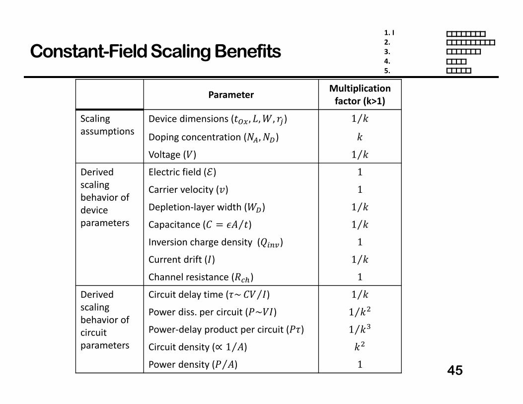
Constant-Field Scaling Benefits
45
ParameterMultiplication
factor (k>1)
Scaling
assumptions
Device dimensions (�=� , 1,2, ��) 1 o⁄Doping concentration (?@, ?%) oVoltage (�) 1 o⁄
Derived
scaling
behavior of
device
parameters
Electric field (�) 1Carrier velocity (i) 1Depletion-layer width (2%) 1 o⁄Capacitance (< A� �⁄ ) 1 o⁄Inversion charge density (B456) 1Current drift (,) 1 o⁄Channel resistance (I'�) 1
Derived
scaling
behavior of
circuit
parameters
Circuit delay time (�~<� ,⁄ ) 1 o⁄Power diss. per circuit ( ~�,) 1 oO⁄Power-delay product per circuit ( �) 1 o¡⁄Circuit density (∝ 1 �⁄ ) oOPower density ( �⁄ ) 1

1. I
2.
3.
4.
5.
Failure of Constant-Field Scaling
46
Since �" cannot be scaled down aggressively, the operating voltage (�%%)
has not been scaled down in proportion to the MOSFET channel length:
Feature Size
(¢£)
Power-Supply
Voltage (�)
Gate Oxide
Thickness (¤)
Oxide Field
(¥� ¦£⁄ )
2 5 350 104
1.2 5 250 2.0
0.8 5 180 2.8
0.5 3.3 120 2.8
0.35 3.3 100 3.3
0.25 2.5 70 3.6

1. I
2.
3.
4.
5.
MOSFET Scaling: Generalized Approach
47
ParameterMultiplication factor
(k>1)
Scaling
assumptions
Device dimensions (�=� , 1,2, ��) 1 o⁄Doping concentration (?@, ?%) §oVoltage (�) § o⁄
Derived scaling
behavior of
device
parameters
Electric field (�) §Depletion-layer width (2%) 1 o⁄Capacitance (< A� �⁄ ) 1 o⁄Inversion charge density (B456) §
Long ch. Vel Sat.
Carrier velocity (i) § 1Current drift (,) §O o⁄ § o⁄
Derived scaling
behavior of
circuit
parameters
Circuit delay time (�~<� ,⁄ ) 1 §o⁄ 1 o⁄Power diss. per circuit ( ~�,) §¡ oO⁄ §O oO⁄Power-delay product per circuit ( �) §O o¡⁄Circuit density (∝ 1 �⁄ ) oOPower density ( �⁄ ) §¡ §O
Electric field
intensity
increases by
a factor § ! 1?¨ C© must
be scaled up
by § to
suppress
short-
channel
effects

1. I
2.
3.
4.
5.
Drain Induced Barrier Lowering (DIBL)
48
As the source and drain get closer, they become electrostatically coupled, so
that the drain bias can affect the potential barrier to carrier diffusion at the
source junction
� VT decreases (i.e. OFF state leakage current increases)
ln ,%
��#
�CG 50��CG 3�
�=� 100¤?@ 3 � 10S��Z¡
������
�����������
������
�����������
Long 1
Short1

1. I
2.
3.
4.
5.
Punchthrough
49
A large drain bias can cause the drain-junction depletion region to merge with
the source-junction depletion region, forming a sub-surface path for current
conduction.� IDsat increases rapidly with VDS
p
�n+ n+
1 ↘
This can be mitigated by doping the semiconductor more heavily in the sub-
surface region, i.e. using a “retrograde” doping profile.

1. I
2.
3.
4.
5.
Source and Drain (S/D) Structure
To minimize the short channel effect and DIBL, we want shallow (small rj) S/D
regions − but the parasitic resistance of these regions increases when rj is
reduced.
where ª = resistivity of the S/D regions
Shallow S/D “extensions” may be used to effectively reduce rj with a relatively
small increase in parasitic resistance
IG «¬'D, IC¬W45 ∝ ª 2��⁄
p
�n+ n+nn

1. I
2.
3.
4.
5.
E - Field Distribution Along the Channel
The lateral electric field peaks at the drain end of the channel.���o can be as high as 106 V/cm
High E-field causes problems:
Damage to oxide interface & bulk
(trapped oxide charge � VT shift)
substrate current due to impact ionization:

1. I
2.
3.
4.
5.
Lightly Doped Drain (LDD) Structure
Lower pn junction doping results in lower peak E-field
� “Hot-carrier” effects are reduced
� Parasitic resistance is increased

1. I
2.
3.
4.
5.
Parasitic Source-Drain Resistance
For short-channel MOSFET,
IDsat0 ∝ VGS – VT , so that
� IDsat is reduced by ~15% in a 0.1 mm MOSFET.
VDsat is increased to VDsat0 + IDsat (RS + RD)
GGGG
SSSS DDDD
RS RD
,%GWX ,%GWXL1 9 ,%GWXIG��# - �"

1. I
2.
3.
4.
5.
Summary:
MOSFET OFF State vs. ON State
54
OFF state (��# $ �"):
• ,%# is limited by the rate at which carriers diffuse across the source
pn junction
• Minimum subthreshold swing S, and DIBL are issues
• ,%# is limited by the rate at which carriers drift across the channel
• Punchthrough is of concern at high drain bias
• ,%#WX increases rapidly with �%#• Parasitic resistances reduce drive current
• source resistance I# reduces effective ��#• source & drain resistances I# & I% reduce effective �%#
ON state (��# ! �"):