si-w electromagnetic calorimeter contribution in … electromagnetic calorimeter contribution in the...
TRANSCRIPT
Didier Lacour – LPNHE – Paris, October 2015 1
Si-W electromagnetic calorimeter
Contribution in the development of an assembly line for highly granular calorimeters with semiconductor readout
Gluing robot system PCB Metrology Electrical tests Quality Insurance Industrialisation of the gluing process
ATLAS High Granularity Timing Device
Physicists: 0.5 FTE J-E. Augustin D. Lacour
Technical staff: 2 FTE J. David : electronic P. Ghislain : mechanic J-F. Huppert : computing L. Lavergne : instrumentation J-M. Parraud : electronic D. Vincent : mechanic

Description of one layer
1PCB 4 wafers

Detector module assembly
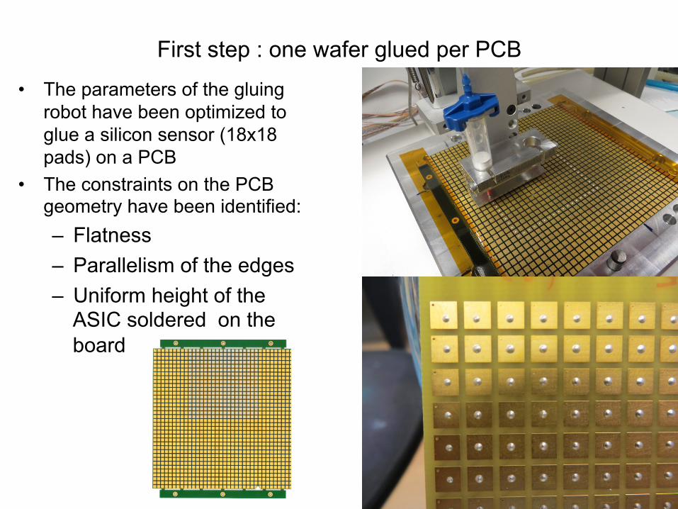
First step : one wafer glued per PCB
• The parameters of the gluing robot have been optimized to glue a silicon sensor (18x18 pads) on a PCB
• The constraints on the PCB geometry have been identified: – Flatness – Parallelism of the edges – Uniform height of the
ASIC soldered on the board
4
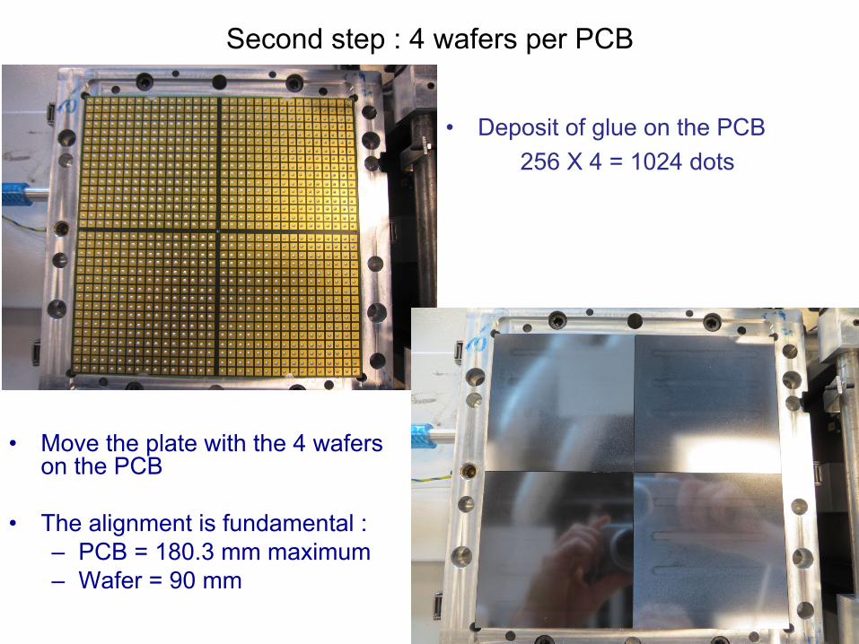
Second step : 4 wafers per PCB
• Move the plate with the 4 wafers on the PCB
• The alignment is fundamental : – PCB = 180.3 mm maximum – Wafer = 90 mm
• Deposit of glue on the PCB 256 X 4 = 1024 dots
5
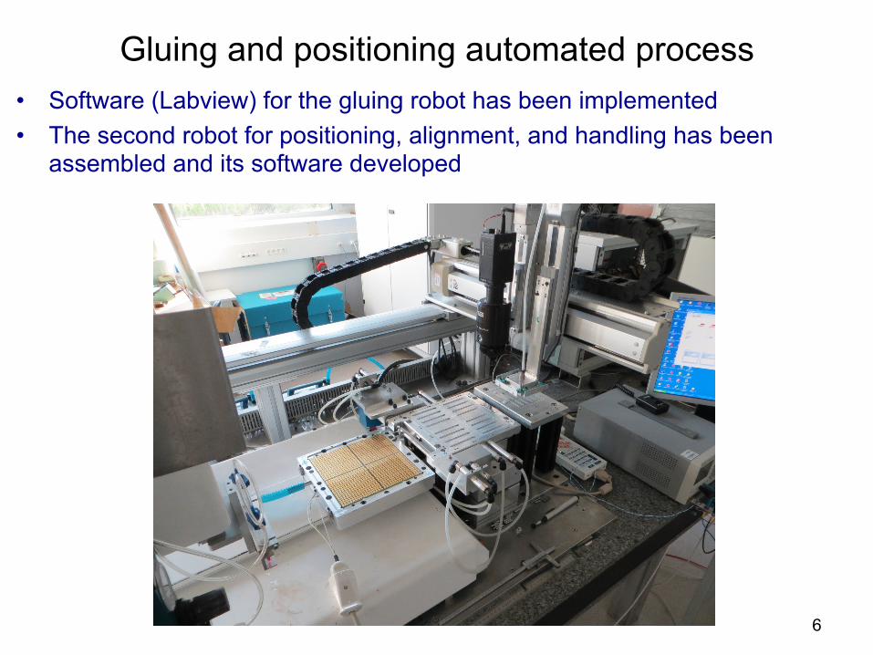
Gluing and positioning automated process • Software (Labview) for the gluing robot has been implemented • The second robot for positioning, alignment, and handling has been
assembled and its software developed
6

Electrical tests bench • A dedicated electrical test system is used
– to control the wafers before gluing – to check the short cuts immediately after gluing – to measure the I(V) curves of each wafer and all 4 wafers
• sourcemeter Keithley 2450 + LLR Bench
7

Electrical tests results
8
• Measurement after gluing onto the PCB – 4 ASU tested, all functional (no short cut). – Waiting for further tests (mip detection)
• I(V) measurement for each wafer before gluing – leakage current 150 nA @ 140 volts
ASU 23 33 34 42
I total (µA)@140V
1.9 11 15 5

PCB Metrology • Development of an automatic process using a coordinate measuring machine
(tri-dim machine) • Before cabling :
– Squaring – Parallel edges – Size – Thickness (flatness in depression) – Flatness
• After cabling : flatness and thickness
9
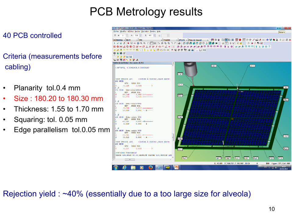
PCB Metrology results
40 PCB controlled Criteria (measurements before cabling) • Planarity tol.0.4 mm • Size : 180.20 to 180.30 mm • Thickness: 1.55 to 1.70 mm • Squaring: tol. 0.05 mm • Edge parallelism tol.0.05 mm
Rejection yield : ~40% (essentially due to a too large size for alveola)
10

Quality insurance
• Task flow completed
• Reception and gluing procedures for 1 and 4 silicon sensors written
• Operation on PCB monitored (follow up)
• Gluing tests registered
• ….
11
Industrialization
• First contact (LLR/LPNHE) with • Offer an industrial gluing process for mass production
• EOLANE would have the ability to dedicate one production line to our gluing process.
• Study of the compatibility of its know-how with – the material (glass then silicon) – the large dimension of PCB – the repeatability of the alignment – the quality of the glue and its heat treatment
12
13
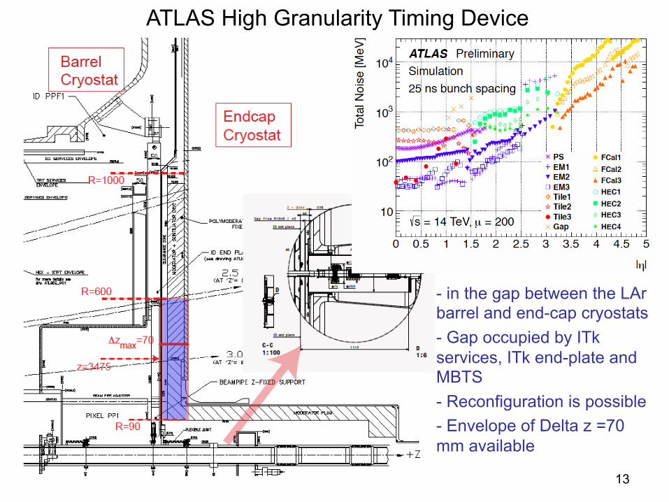
- in the gap between the LAr barrel and end-cap cryostats - Gap occupied by ITk services, ITk end-plate and MBTS - Reconfiguration is possible - Envelope of Delta z =70 mm available
ATLAS High Granularity Timing Device

HGTD ATLAS based on CALICE ATLAS • measurement: t and E • 4 layers in depth (z) • Granularity: 5mm x 5mm
• option: mix with 1cm x 1cm • Same basic structure • Options: No absorber/Absorber
Weaker constraints: • 4 layers in 6cm ~1.5cm per layer:
Chip+PCB+Glue+Wafer=3.225mm, leaves 1cm for cooling and absorber (tungsten 3mm or Pb 5.6mm 1X0 in support structure)
Harsher constraints: • Cooling of sensors -20deg • RadHardness of FE electronics • RadHardness of Glue
(measurements foreseen in 2015-2016)
• Time measurement (order 50 ps) • Smaller peaking time • 40MHz
ILD • Measurement: E (and t) • 30 layers • Absorber: tungsten
• 30 layers in 18cm ~0.6cm per layer
• includes tungsten absorber • Cooling of electronics (passive) • Zero suppression/Power pulsing • 5Hz 1ms bunchtrain
14

Sketch of an implementation in ATLAS
Slabs CALICE-like: • 2ASUs • 3ASUs Alternative: • Single PCB • Pro: less
interconnections • Con: planarity
Support structure (attached to cryostat) • Material? • Alveola? • Direct mounting?
Preserve basic CALICE structure R=110mm, η=4.1 R=600mm, η =2.4
15

16
Time-line and milestones for the implementation of the HGTD

Expressions of interest
Text for IN2P3 circulation
Expression of interest for ATLAS September 4th ATLAS meeting on High Granularity Timing Detector The ATLAS High Granularity Timing Device September 10th at CALICE Collaboration Meeting at MPP Munich “High Granular Timing Device”(HGTD) pour la phase II de ATLAS September 30th ATLAS-IN2P3 - Projets pour 2016
17
Summary • A fully automated gluing process is operational at LPNHE
– Many tests have been performed with glass plates and with one wafer glued per PCB – The system is now used for the standard configuration (4 wafers /PCB) – 4 ASU have been done and will be used in test beam – 3 ASU will be done in the 2 coming weeks
• Quality Insurance and controls put in place – PCB geometrical measurements – Electrical tests – Procedures – Data bookkeeping
• Contacts for industrialization of the gluing process started
• ATLAS HGTD possible contributions - Modules assembly - Characterization of wafers and ASUs: geometry and electric I(U) - Silicon wafers optimisation: design and measurements, simulation (silvaco) - Tests beam of prototypes - Detector geometry optimisation (MC)
18

1 - Demande de crédits sur projet Fournitures et équipements scientifiques : 4000 (pompes 24 volts, plaques de verre haute précision, colle conductrice, maintenance robot) Missions, déplacements colloques et communications : 9000 Informatique (portables, serveurs de manip) : 2000 Salaires (stagiaires) : 3 mois, étudiant instrumentaliste, type M1 ou L3 : 1500 TOTAL : 16500 2 - Demande de crédits sur réseau R&D instrumentation - Détecteurs semi-conducteurs Les équipements : pico-ampèremètre ; onduleur ; salle propre modulaire (plafond soufflant) Les montants : 5000 + 3000 + 10 000 tests des wafers avant et après collage sur PCB ; sécurisation du robot de collage en prévention de coupures de courant ; assurer une qualité optimum du collage des wafers TOTAL : 18 000 3 - Demande de chercheurs CDD 3 ans - Physicien instrumentaliste (Priorité 1 LPNHE) - Participation aux tests en faisceau - Analyse des données - Etudes monte carlo pour l’optimisation des géométries des détecteurs ILD et ATLAS - Mise en place d’études des capteurs silicium grâce à la simulation Silvaco et leurs caractérisations (machine à pointes ou système dédié)
19