silicon-on-sapphire waveguides: mode-converting … document 3283 ... a canon® fpa-3000 ex5 stepper...
TRANSCRIPT

TECHNICAL DOCUMENT 3283 September 2014
Silicon-on-Sapphire Waveguides: Mode-converting Couplers
and Four-Wave Mixing
Sanja Zlatanovic
Randy Shimabukuro Bruce Offord
Bill Jacobs
Approved for public release.
SSC Pacific San Diego, CA 92152-5001

SB
SSC Pacific San Diego, California 92152-5001
K. J. Rothenhaus, CAPT, USN Commanding Officer
C. A. KeeneyExecutive Director
ADMINISTRATIVE INFORMATION
The work described in this report was performed by the Advanced Photonic Technologies Branch (Code 55360) and the Advanced Integrated Circuit Technology Branch (Code 55250), Space and Naval Warfare Systems Center Pacific (SSC Pacific), San Diego, CA. The Naval Innovative Science and Engineering (NISE) Program at SSC Pacific funded this Basic Research project.
This is a work of the United States Government and therefore is not copyrighted. This work may be copied and disseminated without restriction. The citation of trade names and names of manufacturers in this report is not to be construed as official government endorsement or approval of commercial products or services referenced in this report. Canon® is a registered trademark of Canon Inc. Lam® and TCP® are registered trademarks of Lam Research Corporation.
Released by Russel Clement, Acting Head Advanced Photonic Technologies Branch
Under authority of S. Clayton. Acing Head Enterprise Communications and Networks Division

iii
EXECUTIVE SUMMARY
The goal of this project is to design and develop a widely tunable coherent light source in the wavelength range between 3 and 4 m via four-wave mixing in silicon-on-sapphire waveguides. This project will address the Navy need to extend the range of spectrum dominance. Previous investigations show that this spectral range is of interest for applications that include free-space communications, laser radar, optical countermeasures, and remote sensing.
This document summarizes progress made during fiscal year 2014 and specifically includes:
Design, fabrication and performance of mode-converting couplers and silicon-on-sapphire waveguides
Measurements of four-wave mixing in silicon-on-sapphire waveguides

iv
CONTENTS
EXECUTIVE SUMMARY .................................................................................................................. ii
1. BACKGROUND ............................................................................................................................ 1
2. WAVEGUIDE SIMULATIONS AND DESIGN ............................................................................. 2
2.1. WAVEGUIDE DISPERSION ....................................................................................................... 2
2.2. WAVEGUIDE COUPLERS .......................................................................................................... 2
3. FABRICATION PROCESS ...................................................................................................... 4
4. WAVEGUIDE TESTING ........................................................................................................... 6
4.1. PROPAGATION LOSS ................................................................................................................ 6
4.2. HIGH- EFFICIENCY MODE-CONVERTING COUPLERS ..................................................... 8
5. FOUR-WAVE MIXING IN SILICON-ON-SAPPHIRE WAVEGUIDES ....................................... 9
6. CONCLUSIONS ..................................................................................................................... 10
7. REFERENCES ............................................................................................................................ 11
APPENDIX A .............................................................................................................................. 12
Figures
1. Calculated conversion efficiency of four-wave mixing in 1700nm wide silicon-on-sapphire waveguide. Color bar indicates conversion efficiency in decibels ......................................... 2
2. a) Regular-tapered coupler, b) mode converter with high coupling efficiency .......................... 3 3. a) Cross-section of inverse taper tip with pinched profile caused by insufficient O2 flow, and
b) taper created by excess O2 ............................................................................................... 4 4. Cross section of silicon waveguides at the edge of high-efficienc,y mode-converting
coupler ................................................................................................................................... 5 5. a) Regular-tapered coupler before polishing, b) Regular-tapered coupler after polishing ........ 6 6. Waveguide insertion loss .......................................................................................................... 6 7. a) SEM of silicon-on-sapphire waveguide with visible sidewall and top surface roughness,
b) AFM of the waveguide surface showing top surface roughness, c) measurement of surface roughness along red line ....................................................................................... 7
8. Improvement in sidewall roughness by fine-tuning etching conditions ..................................... 7 9. Mode converters with with high coupling efficiency after polishing. Damage is visible ............. 8 10. Four-wave mixing in silicon-on-sapphire waveguides ............................................................. 9

1
1. BACKGROUND
Photonic devices on silicon-on-sapphire have drawn much interest lately because they can operate at longer wavelengths compared to silicon-on-insulator devices. Silicon-on-insulator devices suffer from substantial loss at wavelengths beyond 3.6 m due to the high absorption properties of silicon dioxide. The silicon-on-sapphire platform, however, shows good transparency from the telecom band to the mid-infrared band up to 5 m and is therefore a better choice for longer wavelengths [1, 2, 3].
The main applications of silicon-on-sapphire waveguides in the mid-infrared range between 3 to 4 m are for free-space optical communications and laser radar. The goal of this project is to develop mid-infrared transmitters for these applications by utilizing a four-wave mixing process, therefore compensating for lack of infrastructure in the mid-infrared band. State-of–the-art devices in the mid-infrared band, such as modulators and direct-modulation laser sources, still have inferior perform-ance compared to telecom band devices, therefore hindering the performance of mid-infrared transmitters. Using four-wave mixing, various modulation formats can be transferred directly from the telecom band to the mid-infrared band, thereby enabling high-performance mid-infrared transmitters.
Four-wave mixing processes were previously utilized to generate new wavelengths by leveraging existing sources in the telecom and short-wave infrared bands. Using silicon-on-insulator wave-guides, researchers have demonstrated that sources at wavelengths beyond 2.2 m can be generated using four-wave mixing [4, 5]. Recently, researchers have reported generation of mid-infrared light up to 3.6-m wavelength on a silicon-on-insulator platform [6]. However, as previously mentioned, this platform suffers from material limitations, therefore making silicon-on-sapphire a better choice for longer wavelengths.
The approach presented here involves the four-wave mixing of a pump at a short-wave infrared (SWIR) wavelength around 2 m and signals in telecom band to generate light in the mid-infrared. Simulation data indicate that efficient four-wave mixing can be achieved in the mid-infrared using silicon-on-sapphire waveguides [7]. Pumping silicon at SWIR diminishes parasitic effects such as two-photon absorption that would be detrimental to four-wave mixing efficiency. The main benefits of using four-wave mixing are developing data-encoding capability, wide tenability, and fast sweeping of sources in the mid-infrared.
Efficiency of four-wave mixing process is highly dependent on pump power, making low-loss coupling into the silicon waveguides imperative. Efficient coupling between highly confined modes in silicon waveguides and the large mode of the fiber is a well-known challenge. Here, we present the design and performance of mode converters with high coupling efficiency designed for a silicon-on-sapphire platform. We describe fabrication procedures and current results on the characterization of the waveguides and waveguide couplers. We discuss issues, such as surface roughness, that impede performance of the waveguides and present solutions we plan to implement to solve these issues in the future. Finally, we report results of the first four-wave mixing measurements in silicon-on-sapphire waveguides at the telecom band.
2
2. WAVEGUIDE SIMULATIONS AND DESIGN
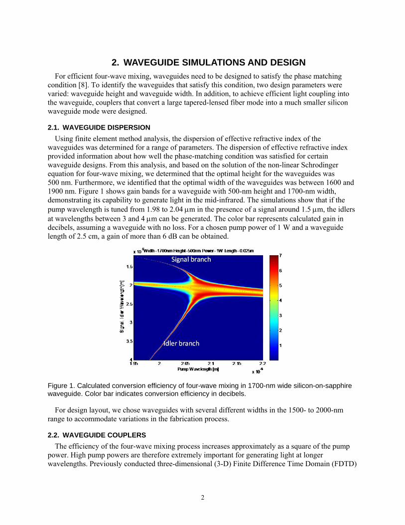
For efficient four-wave mixing, waveguides need to be designed to satisfy the phase matching condition [8]. To identify the waveguides that satisfy this condition, two design parameters were varied: waveguide height and waveguide width. In addition, to achieve efficient light coupling into the waveguide, couplers that convert a large tapered-lensed fiber mode into a much smaller silicon waveguide mode were designed.
2.1. WAVEGUIDE DISPERSION
Using finite element method analysis, the dispersion of effective refractive index of the waveguides was determined for a range of parameters. The dispersion of effective refractive index provided information about how well the phase-matching condition was satisfied for certain waveguide designs. From this analysis, and based on the solution of the non-linear Schrodinger equation for four-wave mixing, we determined that the optimal height for the waveguides was 500 nm. Furthermore, we identified that the optimal width of the waveguides was between 1600 and 1900 nm. Figure 1 shows gain bands for a waveguide with 500-nm height and 1700-nm width, demonstrating its capability to generate light in the mid-infrared. The simulations show that if the pump wavelength is tuned from 1.98 to 2.04 m in the presence of a signal around 1.5 m, the idlers at wavelengths between 3 and 4 m can be generated. The color bar represents calculated gain in decibels, assuming a waveguide with no loss. For a chosen pump power of 1 W and a waveguide length of 2.5 cm, a gain of more than 6 dB can be obtained.
Figure 1. Calculated conversion efficiency of four-wave mixing in 1700-nm wide silicon-on-sapphire waveguide. Color bar indicates conversion efficiency in decibels.
For design layout, we chose waveguides with several different widths in the 1500- to 2000-nm range to accommodate variations in the fabrication process.
2.2. WAVEGUIDE COUPLERS
The efficiency of the four-wave mixing process increases approximately as a square of the pump power. High pump powers are therefore extremely important for generating light at longer wavelengths. Previously conducted three-dimensional (3-D) Finite Difference Time Domain (FDTD)

3
modeling analysis [8] identified two coupler designs: a regular-tapered coupler and a mode converter with a high coupling efficiency.
The regular-tapered couplers were designed to be 150-m long, starting at 8 m at the facet and tapering down to the waveguide width (Figure 2a).
The mode converter with a high coupling efficiency consists of an inverse-tapered silicon waveguide embedded in a larger SiN waveguide. Silicon nitride (SiN) was chosen as a material for the larger waveguide, because of its compatibility with the Complementary Metal–Oxide–Semiconductor CMOS process, its index of refraction (nSiN = 2) that is larger than the index of refraction of sapphire (nsapphire = 1.7) as required for guiding, and its transparency from the telecom to the mid-infrared band. The silicon inverse tapers have a 100-nm-wide tip and are 150-m long. The overlaying SiN waveguide is 5-m wide and 2-m tall (Figure 2b). According to the simulations, mode converters with high coupling efficiency have ~ 3 dB better coupling efficiency than the regular-tapered couplers, but are much more challenging to fabricate on silicon-on-sapphire.
Figure 2. a) Regular-tapered coupler, b) mode converter with high coupling efficiency.
a b

4
3. FABRICATION PROCESS
The starting substrates for fabrication were 6-in silicon-on-sapphire wafers with a 110-nm device layer. These wafers were fabricated using an improvement process that involved annealing the silicon layer to remove defects caused by the lattice mismatch between silicon and sapphire. The desired thickness of the silicon layer is 500 nm according to our design. To achieve this thickness, 390 nm of epitaxial silicon was grown on top of the wafer.
The wafers were then processed using a 0.25-m silicon-on-sapphire process at Defense Microelectronic Research Activity (DMEA). The wafers underwent an initial clean prior to the first masking step. Then they were coated with a 390-nm UV210 photoresist. The wafers were exposed in a Canon® FPA-3000 EX5 stepper at 280 J/m2. Using this energy, the minimum defined feature size (drawn at 0.16 µm) was below 0.14 µm. Silicon was etched all the way to sapphire using a Lam® TCP® 9400 SE etcher. Gas flows were chosen based on the silicon etch rate and resulting profile. We used hydrobromic acid (HBr) as the primary etch gas. Helium oxide (HeO2) was used to introduce oxygen and to control bowing in the etch profile. Insufficient O2 flows can lead to severe bowing while excess oxygen (O2) increased the rate of passivation layer formation, which reduced the anisotropy of the sidewalls (Figure 3).
Figure 3. a) Cross-section of inverse taper tip with pinched profile caused by insufficient O2 flow, and b) taper created by excess O2.
To reduce the critical dimension (CD) at the end of the silicon taper to specification limits of 0.1 ± 0.02 µm, we introduced a chlorine (Cl2) step that reduced the lateral dimensions of the photo-resist enough to achieve the CD specification limits of the final etch. A dilute hydrofluoric acid dip (100 sec in 100:1 hydrofluoric acid (HF) was required to completely remove the thin sidewall passivation film (SiO2) created by the silicon etch.
The remaining photoresist was ashed at each mask step. This step was followed by an automated standard clean (sulfuric/SC1/SC2).
In the next step, oxide was deposited using plasma-enhanced chemical vapor deposition (PECVD). For the oxide masking step, 600-nm UV210 photoresist was spun on the samples. Wafers were exposed in the EX5 stepper at 180 J/m2.
We also used PECVD to deposit SiN. The PECVD nitride deposited is not very stoichiometric (0.8 to 1.0:1 vs. 0.75:1 for thermal Si3N4), but has less tensile stress than a thermal film (3.4 Gdyn/cm2 vs. 15 Gdyn/cm2 on Si).
a b

5
We increased the photoresist thickness for the nitride mask to 970 nm because selectivity between nitride and photoresist was poor. Wafers were exposed in the EX5 stepper at 320 J/m2.
Wafers were then etched with HBr/CF4 to remove nitride with much higher selectivity over oxide. This allowed the very thick remaining regions of nitride to be removed without etching through the pad oxide and into the silicon.
After photoresist removal, we removed the remaining oxide that protected the silicon waveguides using a 6:1 buffered oxide etch (BOE). Figure 4 shows the cross section of a fabricated waveguide.
Photoresist measuring 2.4 µm was then deposited prior to removing the wafer from the foundry. We added the photoresist to create a passivation layer to stabilize the silicon nitride waveguides during stressful polishing steps, and to protect the die surface from scratches and particles during post-foundry processing.
Figure 4. Cross section of silicon waveguides at the edge of high-efficiency mode-converting coupler.

6
4. WAVEGUIDE TESTING
4.1. PROPAGATION LOSS
Figure 5 shows regular-tapered couplers before and after polishing with grit. During polishing the waveguides were protected with a layer of photoresist that was later removed. Polishing of regular-tapered couplers produced clean facets for light coupling with high yield.
Figure 5. a) Regular-tapered coupler before polishing, b) Regular-tapered coupler after polishing
Due to the good quality of the regular-tapered couplers observed over all the chips, we chose the waveguides with regular-tapered fibers to measure propagation loss. We measured the total insertion loss of the waveguides using the cut-back method on the waveguides with regular-tapered couplers. We tested the waveguides with three different lengths: 5.167 mm (short), 9.908 mm (medium), and 16 mm (long). Because of the good quality of the couplers, we can assume that coupling loss for all the regular-tapered couplers is similar, and therefore causes little variation in the total insertion loss measurement. Therefore, the variations can be completely contributed to the difference in the waveguide length.
To measure insertion loss, we coupled the light into the waveguides and out of the waveguides using tapered-lensed fibers. Insertion loss values are plotted in Figure 6.
Figure 6. Waveguide insertion loss.
The slope of the curve indicates that propagation loss is 15.21 dB/cm of waveguide length. To confirm propagation loss measurements, we performed another set of measurements using an optical backscatter reflectometer (OBR). The loss measured by OBR was ~ 17 dB/cm, confirming the high value measured using the cut-back method. This high value of propagation loss indicated that some issues exist with the waveguides and the fabrication process. Examining the waveguides under a scanning electron microscope (SEM) and atomic force microscope (AFM) revealed that the waveguide sidewalls and top surface had substantial roughness (Figure 7). Visible striation roughness
a b

7
exists on the sidewalls, and the top surface has roughness due to epi defects and potential contaminants. Propagation loss of the waveguides can be calculated using numerical model developed in [9]. From SEMs and AFMs, the roughness amplitude of both top surface and sidewalls was on the order of 10 nm. Standard deviation was 4.8 and 4.5 nm for top surface and sidewall roughness, respectively. Correlation length for top surface roughness was 800 nm and for sidewalls was 50 nm. As shown in Appendix A, these values give propagation loss of 16 dB/cm, consistent with our propagation loss measurements.
Figure 7. a) SEM of silicon-on-sapphire waveguide with visible sidewall and top surface roughness, b) AFM of the waveguide surface showing top surface roughness, c) measurement of surface roughness along red line.
Based on the insertion and propagation loss measurements, coupling loss for the regular-tapered couplers was 8.6 ±0.6 dB/coupler.
To reduce the waveguide propagation loss, we plan to implement a hard mask and tune etching conditions to reduce sidewall roughness in future batches. Initial tests with new etching conditions, followed by post oxidation and removal of oxide, significantly reduced the sidewall striation (Figure 8). Top surface roughness can be reduced by plasma etching and annealing in hydrogen plasma.
Figure 8. Improvement in sidewall roughness by fine-tuning etching conditions.
a b
c

8
4.2. HIGH-EFFICIENCY MODE-CONVERTING COUPLERS
Figure 9 shows mode converters with high coupling efficiency after their facets were polished. Some of the couplers suffered damage to the silicon nitride waveguide that was due to the stress imposed on the nitride during the polishing process. This caused a low yield of good quality mode-converting couplers. We were able to couple light into the waveguides with damaged couplers as well, but with large loss. For the couplers that did not exhibit visible signs of damage, the coupling loss measured 4.8 ±1.1 dB/coupler. This presents near 4-dB improvement in coupling loss compared to the regular-tapered couplers. To increase the fabrication yield of good quality mode converters with high coupling efficiency, we tested an alternative fabrication method that involves cutting of nitride waveguides using focused ion beam (FIB) prior to polishing. The SiN waveguides did not break during the polishing step when this method was applied, proving that a notch or cut before polishing relieves film stress.
Figure 9. Mode converters with high coupling efficiency after polishing. Damage is visible.

9
5. FOUR-WAVE MIXING IN SILICON-ON-SAPPHIRE WAVEGUIDES
We measured four-wave mixing in the silicon-on-sapphire waveguides with the short 5.167-mm length. A continuous wave pump at 1552.85 nm with power of 100 mW was combined with tunable signals using a wavelength division multiplexer (WDM) coupler. The light was coupled into and out of the waveguides using a tapered-lensed fiber. We measured four-wave mixing conversion efficiency of -42 dB (Figure 10). This corresponds well to theoretical predictions that consider the ~ 16-dB loss in the waveguides. Improving the propagation loss will considerably improve four-wave mixing efficiency.
Figure10. Four-wave mixing in silicon-on-sapphire waveguides.
Signals
Idlers

10
6. CONCLUSIONS
We have fabricated silicon-on-sapphire waveguides with mode converters with high coupling efficiency that improved coupling efficiency by ~ 4 dB compared to the regular-tapered couplers. The fabricated waveguides exhibited high propagation loss due to surface roughness. Modifications of the fabrication process reduce the surface roughness and we will implement this process in the next waveguide fabrication batch. In addition, implementing focused ion beam (FIB) cutting prior to facet polishing provided less damage and potentially better yield for fabricating the mode converters with high coupling efficiency. We have also demonstrated the first experimental four-wave mixing in silicon-on-sapphire waveguides.

11
7. REFERENCES
[1] T. Baehr-Jones, A. Spott, R. Ilic, A. Spott, B. Penkov, W. Asher, and M. Hochberg. 2010. “Silicon-on-Sapphire Integrated Waveguides for the Mid-infrared,” Optics Express 18:12127‒12135.
[2[ F. Li, S. D. Jackson, C. Grillet, E. Magi, D. Hudson, S. J. Madden, Y. Moghe, C. O’Brien, A. Read, S. G. Duvall, P. Atanackovic, B. J. Eggleton, and D. J. Moss. 2011. “Low Propagation Loss Silicon-on-Sapphire Waveguides for the Mid-infrared,” Optics Express 19:15212‒15220.
[3] R. Shankar, B. Irfan, and L. Marko Lončar. 2013 “Integrated High-quality Factor Silicon-on-Sapphire Ring Resonators for the Mid-infrared,” Applied Physics Letters 102(5):051108.
[4] S. Zlatanovic, J. S. Park, S. Moro, J. M. C. Boggio, I. B. Divliansky, N. Alic, S. Mookherjea, and S. Radic. 2010. “Mid-infrared Wavelength Conversion in Silicon Waveguides using Ultracompact Telecom-band-derived Pump Source,” Nature Photonics 4(8):561‒564.
[5] X. Liu, R. M. Osgood, Jr, Y. A. Vlasov, and W. M. J. Green. 2010. “Mid-infrared Optical
Parametric Amplifier using Silicon Nanophotonic Waveguides,” Nature Photonics 4(8): 557‒560.
[6] B. Kuyken, P. Verheyen, P. Tannouri, X. Liu, J. Van Campenhout, R. Baets, W. M. Green, and G. Roelkens. 2014. “Generation of 3.6 μm Radiation and Telecom-band Amplification by Four-wave Mixing in a Silicon Waveguide with Normal Group Velocity Dispersion,” Optics Letters 39(6): 1349‒1352.
[7] En-Kuang Tien, Y. Huang, S. Gao, Q. Song, F. Qian, SK Kalyoncu, and O. Boyraz. 2010. “Discrete Parametric Band Conversion in Silicon for Mid-infrared Applications,” Optics Express 18(21):21981-21989.
[8] S. Zlatanovic, B. Neuner III, B. Jacobs, B. Offord, R. Shimabukuro. 2013. “Silicon-on-Sapphire Waveguides for Widely Tunable Coherent Mid-IR Sources.” Technical Document 3275. Space and Naval Warfare Systems Center Pacific (SSC Pacific), San Diego, CA.
[9] F. Grillot, L. Vivien, S. Laval, and E. Cassan. 2006. “Propagation Loss in Single-mode Ultrasmall Square Silicon-on-Insulator Optical Waveguides,” Journal of Lightwave Technology 24(2):891‒896.

A-1
APPENDIX A
Propagation loss caused by surface roughness was calculated according to [9].
Linear loss was defined as
σ2
k0√2d4ncgf x ,
where , k , k , k ,
, , √
, Δ
where σ is standard deviation of surface roughness, k is propagation constant in air, d is half a width or half a height of the waveguide, is core refractive index, n is cladding refractive index, is
effective index of the waveguide mode, and is roughness correlation length.
Values for refractive indices are n = 3.47, n = 1 for top surface, and n = 3.26 at 1550 nm for 2000-nm wide and 500-nm tall waveguide.
The fabricated waveguides have the following values measured for surface roughness and d.
σ[nm] L [nm] d[nm] Top surface 4.8 800 250 Sidewalls 4.5 50 1000
Total propagation loss was calculated to be ~16dB/cm of which 8.5dB/cm is contributed to sidewall roughness and 7.5dB/cm to top surface roughness.

5f. WORK UNIT NUMBER
REPORT DOCUMENTATION PAGEForm Approved
OMB No. 0704-01-0188
The public reporting burden for this collection of information is estimated to average 1 hour per response, including the time for reviewing instructions, searching existing data sources, gathering and maintaining the data needed, and completing and reviewing the collection of information. Send comments regarding this burden estimate or any other aspect of this collection of information, including suggestions for reducing the burden to Department of Defense, Washington Headquarters Services Directorate for Information Operations and Reports (0704-0188), 1215 Jefferson Davis Highway, Suite 1204, Arlington VA 22202-4302. Respondents should be aware that notwithstanding any other provision of law, no person shall be subject to any penalty for failing to comply with a collection of information if it does not display a currently valid OMB control number. PLEASE DO NOT RETURN YOUR FORM TO THE ABOVE ADDRESS.
1. REPORT DATE (DD-MM-YYYY) 2. REPORT TYPE 3. DATES COVERED (From - To)
4. TITLE AND SUBTITLE 5a. CONTRACT NUMBER
5b. GRANT NUMBER
5c. PROGRAM ELEMENT NUMBER
5d. PROJECT NUMBER
5e. TASK NUMBER
6. AUTHORS
7. PERFORMING ORGANIZATION NAME(S) AND ADDRESS(ES) 8. PERFORMING ORGANIZATION REPORT NUMBER
10. SPONSOR/MONITOR’S ACRONYM(S)
11. SPONSOR/MONITOR’S REPORT NUMBER(S)
9. SPONSORING/MONITORING AGENCY NAME(S) AND ADDRESS(ES)
12. DISTRIBUTION/AVAILABILITY STATEMENT
13. SUPPLEMENTARY NOTES
14. ABSTRACT
15. SUBJECT TERMS
16. SECURITY CLASSIFICATION OF: a. REPORT b. ABSTRACT c. THIS PAGE
17. LIMITATION OF ABSTRACT
18. NUMBER OF PAGES
19a. NAME OF RESPONSIBLE PERSON
19B. TELEPHONE NUMBER (Include area code)
Standard Form 298 (Rev. 8/98)Prescribed by ANSI Std. Z39.18
September 2014 Final
Silicon-on-Sapphire Waveguides: Mode-converting Couplers and Four-wave Mixing
Sanja Zlatanovic Bruce Offord Randy Shimabukuro Bill Jacobs
SSC Pacific, 53560 Hull Street, San Diego, CA 92152–5001
TD 3283
Naval Innovative Science and Engineering (NISE) Program (Basic Research) SSC Pacific, 53560 Hull Street, San Diego, CA 92152–5001
Approved for public release.
This is work of the United States Government and therefore is not copyrighted. This work may be copied and disseminated without restriction.
The goal of this project is to design and develop a widely tunable coherent light source in the wavelength range between 3 and 4 µm via four-wave mixing in silicon-on-sapphire waveguides. This project will address the Navy need to extend the range of spectrum dominance. Previous investigations show that this spectral range is of interest for applications that include free-space communications, laser radar, optical countermeasures, and remote sensing.
This document summarizes progress made during fiscal year 2014, and specifically includes:
Design, fabrication, and performance of mode-converting couplers and silicon-on-sapphire waveguides
Measurements of four-wave mixing in silicon-on-sapphire waveguides Mission Area: Advanced Photonic Technologies silicon-on-sapphire waveguides spectrum dominance high-efficiency couplers Four-wave mixing mode converters
Sanja Zlatanovic
U U U U 19 (619) 767-4078

INITIAL DISTRIBUTION
84300 Library (2) 85300 Archive/Stock (1) 55250 B. Offord (1) 55360 S. Zlatanovic (1) 55360 R. Shimabukuro (1) 55360 Bill Jacobs (1)
Defense Technical Information Center Fort Belvoir, VA 22060–6218 (1)

Approved for public release.
SSC Pacific San Diego, CA 92152-5001