silicon photomultipliers: dark current and its statistical spread
TRANSCRIPT


SSeennssoorrss && TTrraannssdduucceerrss
Volume 14-1, Special Issue March 2012
wwwwww..sseennssoorrssppoorrttaall..ccoomm ISSN 1726-5479
Editors-in-Chief: Sergey Y. Yurish, tel.: +34 93 413 7941, e-mail: [email protected]
Editors for Western Europe Meijer, Gerard C.M., Delft University of Technology, The Netherlands Ferrari, Vittorio, Universitá di Brescia, Italy
Editor for Eastern Europe Sachenko, Anatoly, Ternopil State Economic University, Ukraine
Editors for North America Datskos, Panos G., Oak Ridge National Laboratory, USA Fabien, J. Josse, Marquette University, USA Katz, Evgeny, Clarkson University, USA
Editor South America Costa-Felix, Rodrigo, Inmetro, Brazil
Editor for Africa Maki K.Habib, American University in Cairo, Egypt Editor for Asia Ohyama, Shinji, Tokyo Institute of Technology, Japan
Editor for Asia-Pacific Mukhopadhyay, Subhas, Massey University, New Zealand
Editorial Advisory Board
Abdul Rahim, Ruzairi, Universiti Teknologi, Malaysia Ahmad, Mohd Noor, Nothern University of Engineering, Malaysia Annamalai, Karthigeyan, National Institute of Advanced Industrial Science
and Technology, Japan Arcega, Francisco, University of Zaragoza, Spain Arguel, Philippe, CNRS, France Ahn, Jae-Pyoung, Korea Institute of Science and Technology, Korea Arndt, Michael, Robert Bosch GmbH, Germany Ascoli, Giorgio, George Mason University, USA Atalay, Selcuk, Inonu University, Turkey Atghiaee, Ahmad, University of Tehran, Iran Augutis, Vygantas, Kaunas University of Technology, Lithuania Avachit, Patil Lalchand, North Maharashtra University, India Ayesh, Aladdin, De Montfort University, UK Azamimi, Azian binti Abdullah, Universiti Malaysia Perlis, Malaysia Bahreyni, Behraad, University of Manitoba, Canada Baliga, Shankar, B., General Monitors Transnational, USA Baoxian, Ye, Zhengzhou University, China Barford, Lee, Agilent Laboratories, USA Barlingay, Ravindra, RF Arrays Systems, India Basu, Sukumar, Jadavpur University, India Beck, Stephen, University of Sheffield, UK Ben Bouzid, Sihem, Institut National de Recherche Scientifique, Tunisia Benachaiba, Chellali, Universitaire de Bechar, Algeria Binnie, T. David, Napier University, UK Bischoff, Gerlinde, Inst. Analytical Chemistry, Germany Bodas, Dhananjay, IMTEK, Germany Borges Carval, Nuno, Universidade de Aveiro, Portugal Bouchikhi, Benachir, University Moulay Ismail, Morocco Bousbia-Salah, Mounir, University of Annaba, Algeria Bouvet, Marcel, CNRS – UPMC, France Brudzewski, Kazimierz, Warsaw University of Technology, Poland Cai, Chenxin, Nanjing Normal University, China Cai, Qingyun, Hunan University, China Calvo-Gallego, Jaime, Universidad de Salamanca, Spain Campanella, Luigi, University La Sapienza, Italy Carvalho, Vitor, Minho University, Portugal Cecelja, Franjo, Brunel University, London, UK Cerda Belmonte, Judith, Imperial College London, UK Chakrabarty, Chandan Kumar, Universiti Tenaga Nasional, Malaysia Chakravorty, Dipankar, Association for the Cultivation of Science, India Changhai, Ru, Harbin Engineering University, China Chaudhari, Gajanan, Shri Shivaji Science College, India Chavali, Murthy, N.I. Center for Higher Education, (N.I. University), India Chen, Jiming, Zhejiang University, China Chen, Rongshun, National Tsing Hua University, Taiwan Cheng, Kuo-Sheng, National Cheng Kung University, Taiwan Chiang, Jeffrey (Cheng-Ta), Industrial Technol. Research Institute, Taiwan Chiriac, Horia, National Institute of Research and Development, Romania Chowdhuri, Arijit, University of Delhi, India Chung, Wen-Yaw, Chung Yuan Christian University, Taiwan Corres, Jesus, Universidad Publica de Navarra, Spain Cortes, Camilo A., Universidad Nacional de Colombia, Colombia Courtois, Christian, Universite de Valenciennes, France Cusano, Andrea, University of Sannio, Italy D'Amico, Arnaldo, Università di Tor Vergata, Italy De Stefano, Luca, Institute for Microelectronics and Microsystem, Italy Deshmukh, Kiran, Shri Shivaji Mahavidyalaya, Barshi, India Dickert, Franz L., Vienna University, Austria Dieguez, Angel, University of Barcelona, Spain Dighavkar, C. G., M.G. Vidyamandir’s L. V.H. College, India Dimitropoulos, Panos, University of Thessaly, Greece
Ding, Jianning, Jiangsu Polytechnic University, China Djordjevich, Alexandar, City University of Hong Kong, Hong Kong Donato, Nicola, University of Messina, Italy Donato, Patricio, Universidad de Mar del Plata, Argentina Dong, Feng, Tianjin University, China Drljaca, Predrag, Instersema Sensoric SA, Switzerland Dubey, Venketesh, Bournemouth University, UK Enderle, Stefan, Univ.of Ulm and KTB Mechatronics GmbH, Germany Erdem, Gursan K. Arzum, Ege University, Turkey Erkmen, Aydan M., Middle East Technical University, Turkey Estelle, Patrice, Insa Rennes, France Estrada, Horacio, University of North Carolina, USA Faiz, Adil, INSA Lyon, France Fericean, Sorin, Balluff GmbH, Germany Fernandes, Joana M., University of Porto, Portugal Francioso, Luca, CNR-IMM Institute for Microelectronics and Microsystems, Italy Francis, Laurent, University Catholique de Louvain, Belgium Fu, Weiling, South-Western Hospital, Chongqing, China Gaura, Elena, Coventry University, UK Geng, Yanfeng, China University of Petroleum, China Gole, James, Georgia Institute of Technology, USA Gong, Hao, National University of Singapore, Singapore Gonzalez de la Rosa, Juan Jose, University of Cadiz, Spain Granel, Annette, Goteborg University, Sweden Graff, Mason, The University of Texas at Arlington, USA Guan, Shan, Eastman Kodak, USA Guillet, Bruno, University of Caen, France Guo, Zhen, New Jersey Institute of Technology, USA Gupta, Narendra Kumar, Napier University, UK Hadjiloucas, Sillas, The University of Reading, UK Haider, Mohammad R., Sonoma State University, USA Hashsham, Syed, Michigan State University, USA Hasni, Abdelhafid, Bechar University, Algeria Hernandez, Alvaro, University of Alcala, Spain Hernandez, Wilmar, Universidad Politecnica de Madrid, Spain Homentcovschi, Dorel, SUNY Binghamton, USA Horstman, Tom, U.S. Automation Group, LLC, USA Hsiai, Tzung (John), University of Southern California, USA Huang, Jeng-Sheng, Chung Yuan Christian University, Taiwan Huang, Star, National Tsing Hua University, Taiwan Huang, Wei, PSG Design Center, USA Hui, David, University of New Orleans, USA Jaffrezic-Renault, Nicole, Ecole Centrale de Lyon, France James, Daniel, Griffith University, Australia Janting, Jakob, DELTA Danish Electronics, Denmark Jiang, Liudi, University of Southampton, UK Jiang, Wei, University of Virginia, USA Jiao, Zheng, Shanghai University, China John, Joachim, IMEC, Belgium Kalach, Andrew, Voronezh Institute of Ministry of Interior, Russia Kang, Moonho, Sunmoon University, Korea South Kaniusas, Eugenijus, Vienna University of Technology, Austria Katake, Anup, Texas A&M University, USA Kausel, Wilfried, University of Music, Vienna, Austria Kavasoglu, Nese, Mugla University, Turkey Ke, Cathy, Tyndall National Institute, Ireland Khelfaoui, Rachid, Université de Bechar, Algeria Khan, Asif, Aligarh Muslim University, Aligarh, India Kim, Min Young, Kyungpook National University, Korea South Ko, Sang Choon, Electronics. and Telecom. Research Inst., Korea South Kotulska, Malgorzata, Wroclaw University of Technology, Poland Kockar, Hakan, Balikesir University, Turkey

Kong, Ing, RMIT University, Australia Kratz, Henrik, Uppsala University, Sweden Krishnamoorthy, Ganesh, University of Texas at Austin, USA Kumar, Arun, University of Delaware, Newark, USA Kumar, Subodh, National Physical Laboratory, India Kung, Chih-Hsien, Chang-Jung Christian University, Taiwan Lacnjevac, Caslav, University of Belgrade, Serbia Lay-Ekuakille, Aime, University of Lecce, Italy Lee, Jang Myung, Pusan National University, Korea South Lee, Jun Su, Amkor Technology, Inc. South Korea Lei, Hua, National Starch and Chemical Company, USA Li, Fengyuan (Thomas), Purdue University, USA Li, Genxi, Nanjing University, China Li, Hui, Shanghai Jiaotong University, China Li, Xian-Fang, Central South University, China Li, Yuefa, Wayne State University, USA Liang, Yuanchang, University of Washington, USA Liawruangrath, Saisunee, Chiang Mai University, Thailand Liew, Kim Meow, City University of Hong Kong, Hong Kong Lin, Hermann, National Kaohsiung University, Taiwan Lin, Paul, Cleveland State University, USA Linderholm, Pontus, EPFL - Microsystems Laboratory, Switzerland Liu, Aihua, University of Oklahoma, USA Liu Changgeng, Louisiana State University, USA Liu, Cheng-Hsien, National Tsing Hua University, Taiwan Liu, Songqin, Southeast University, China Lodeiro, Carlos, University of Vigo, Spain Lorenzo, Maria Encarnacio, Universidad Autonoma de Madrid, Spain Lukaszewicz, Jerzy Pawel, Nicholas Copernicus University, Poland Ma, Zhanfang, Northeast Normal University, China Majstorovic, Vidosav, University of Belgrade, Serbia Malyshev, V.V., National Research Centre ‘Kurchatov Institute’, Russia Marquez, Alfredo, Centro de Investigacion en Materiales Avanzados, Mexico Matay, Ladislav, Slovak Academy of Sciences, Slovakia Mathur, Prafull, National Physical Laboratory, India Maurya, D.K., Institute of Materials Research and Engineering, Singapore Mekid, Samir, University of Manchester, UK Melnyk, Ivan, Photon Control Inc., Canada Mendes, Paulo, University of Minho, Portugal Mennell, Julie, Northumbria University, UK Mi, Bin, Boston Scientific Corporation, USA Minas, Graca, University of Minho, Portugal Moghavvemi, Mahmoud, University of Malaya, Malaysia Mohammadi, Mohammad-Reza, University of Cambridge, UK Molina Flores, Esteban, Benemérita Universidad Autónoma de Puebla,
Mexico Moradi, Majid, University of Kerman, Iran Morello, Rosario, University "Mediterranea" of Reggio Calabria, Italy Mounir, Ben Ali, University of Sousse, Tunisia Mrad, Nezih, Defence R&D, Canada Mulla, Imtiaz Sirajuddin, National Chemical Laboratory, Pune, India Nabok, Aleksey, Sheffield Hallam University, UK Neelamegam, Periasamy, Sastra Deemed University, India Neshkova, Milka, Bulgarian Academy of Sciences, Bulgaria Oberhammer, Joachim, Royal Institute of Technology, Sweden Ould Lahoucine, Cherif, University of Guelma, Algeria Pamidighanta, Sayanu, Bharat Electronics Limited (BEL), India Pan, Jisheng, Institute of Materials Research & Engineering, Singapore Park, Joon-Shik, Korea Electronics Technology Institute, Korea South Penza, Michele, ENEA C.R., Italy Pereira, Jose Miguel, Instituto Politecnico de Setebal, Portugal Petsev, Dimiter, University of New Mexico, USA Pogacnik, Lea, University of Ljubljana, Slovenia Post, Michael, National Research Council, Canada Prance, Robert, University of Sussex, UK Prasad, Ambika, Gulbarga University, India Prateepasen, Asa, Kingmoungut's University of Technology, Thailand Pugno, Nicola M., Politecnico di Torino, Italy Pullini, Daniele, Centro Ricerche FIAT, Italy Pumera, Martin, National Institute for Materials Science, Japan Radhakrishnan, S. National Chemical Laboratory, Pune, India Rajanna, K., Indian Institute of Science, India Ramadan, Qasem, Institute of Microelectronics, Singapore Rao, Basuthkar, Tata Inst. of Fundamental Research, India Raoof, Kosai, Joseph Fourier University of Grenoble, France Rastogi Shiva, K. University of Idaho, USA Reig, Candid, University of Valencia, Spain Restivo, Maria Teresa, University of Porto, Portugal Robert, Michel, University Henri Poincare, France Rezazadeh, Ghader, Urmia University, Iran Royo, Santiago, Universitat Politecnica de Catalunya, Spain Rodriguez, Angel, Universidad Politecnica de Cataluna, Spain Rothberg, Steve, Loughborough University, UK Sadana, Ajit, University of Mississippi, USA Sadeghian Marnani, Hamed, TU Delft, The Netherlands Sapozhnikova, Ksenia, D.I.Mendeleyev Institute for Metrology, Russia Sandacci, Serghei, Sensor Technology Ltd., UK
Saxena, Vibha, Bhbha Atomic Research Centre, Mumbai, India Schneider, John K., Ultra-Scan Corporation, USA Sengupta, Deepak, Advance Bio-Photonics, India Seif, Selemani, Alabama A & M University, USA Seifter, Achim, Los Alamos National Laboratory, USA Shah, Kriyang, La Trobe University, Australia Sankarraj, Anand, Detector Electronics Corp., USA Silva Girao, Pedro, Technical University of Lisbon, Portugal Singh, V. R., National Physical Laboratory, India Slomovitz, Daniel, UTE, Uruguay Smith, Martin, Open University, UK Soleymanpour, Ahmad, Damghan Basic Science University, Iran Somani, Prakash R., Centre for Materials for Electronics Technol., India Sridharan, M., Sastra University, India Srinivas, Talabattula, Indian Institute of Science, Bangalore, India Srivastava, Arvind K., NanoSonix Inc., USA Stefan-van Staden, Raluca-Ioana, University of Pretoria, South Africa Stefanescu, Dan Mihai, Romanian Measurement Society, Romania Sumriddetchka, Sarun, National Electronics and Computer Technology Center,
Thailand Sun, Chengliang, Polytechnic University, Hong-Kong Sun, Dongming, Jilin University, China Sun, Junhua, Beijing University of Aeronautics and Astronautics, China Sun, Zhiqiang, Central South University, China Suri, C. Raman, Institute of Microbial Technology, India Sysoev, Victor, Saratov State Technical University, Russia Szewczyk, Roman, Industrial Research Inst. for Automation and Measurement,
Poland Tan, Ooi Kiang, Nanyang Technological University, Singapore, Tang, Dianping, Southwest University, China Tang, Jaw-Luen, National Chung Cheng University, Taiwan Teker, Kasif, Frostburg State University, USA Thirunavukkarasu, I., Manipal University Karnataka, India Thumbavanam Pad, Kartik, Carnegie Mellon University, USA Tian, Gui Yun, University of Newcastle, UK Tsiantos, Vassilios, Technological Educational Institute of Kaval, Greece Tsigara, Anna, National Hellenic Research Foundation, Greece Twomey, Karen, University College Cork, Ireland Valente, Antonio, University, Vila Real, - U.T.A.D., Portugal Vanga, Raghav Rao, Summit Technology Services, Inc., USA Vaseashta, Ashok, Marshall University, USA Vazquez, Carmen, Carlos III University in Madrid, Spain Vieira, Manuela, Instituto Superior de Engenharia de Lisboa, Portugal Vigna, Benedetto, STMicroelectronics, Italy Vrba, Radimir, Brno University of Technology, Czech Republic Wandelt, Barbara, Technical University of Lodz, Poland Wang, Jiangping, Xi'an Shiyou University, China Wang, Kedong, Beihang University, China Wang, Liang, Pacific Northwest National Laboratory, USA Wang, Mi, University of Leeds, UK Wang, Shinn-Fwu, Ching Yun University, Taiwan Wang, Wei-Chih, University of Washington, USA Wang, Wensheng, University of Pennsylvania, USA Watson, Steven, Center for NanoSpace Technologies Inc., USA Weiping, Yan, Dalian University of Technology, China Wells, Stephen, Southern Company Services, USA Wolkenberg, Andrzej, Institute of Electron Technology, Poland Woods, R. Clive, Louisiana State University, USA Wu, DerHo, National Pingtung Univ. of Science and Technology, Taiwan Wu, Zhaoyang, Hunan University, China Xiu Tao, Ge, Chuzhou University, China Xu, Lisheng, The Chinese University of Hong Kong, Hong Kong Xu, Sen, Drexel University, USA Xu, Tao, University of California, Irvine, USA Yang, Dongfang, National Research Council, Canada Yang, Shuang-Hua, Loughborough University, UK Yang, Wuqiang, The University of Manchester, UK Yang, Xiaoling, University of Georgia, Athens, GA, USA Yaping Dan, Harvard University, USA Ymeti, Aurel, University of Twente, Netherland Yong Zhao, Northeastern University, China Yu, Haihu, Wuhan University of Technology, China Yuan, Yong, Massey University, New Zealand Yufera Garcia, Alberto, Seville University, Spain Zakaria, Zulkarnay, University Malaysia Perlis, Malaysia Zagnoni, Michele, University of Southampton, UK Zamani, Cyrus, Universitat de Barcelona, Spain Zeni, Luigi, Second University of Naples, Italy Zhang, Minglong, Shanghai University, China Zhang, Qintao, University of California at Berkeley, USA Zhang, Weiping, Shanghai Jiao Tong University, China Zhang, Wenming, Shanghai Jiao Tong University, China Zhang, Xueji, World Precision Instruments, Inc., USA Zhong, Haoxiang, Henan Normal University, China Zhu, Qing, Fujifilm Dimatix, Inc., USA Zorzano, Luis, Universidad de La Rioja, Spain Zourob, Mohammed, University of Cambridge, UK
Sensors & Transducers Journal (ISSN 1726-5479) is a peer review international journal published monthly online by International Frequency Sensor Association (IFSA).
Available in electronic and on CD. Copyright © 2012 by International Frequency Sensor Association. All rights reserved.
SSeennssoorrss && TTrraannssdduucceerrss JJoouurrnnaall
CCoonntteennttss
Volume 14-1 Special Issue March 2012
www.sensorsportal.com ISSN 1726-5479
Research Articles
Physical and Chemical Sensors & Wireless Sensor Networks (Foreword) Sergey Y. Yurish, Petre Dini............................................................................................................... I From Smart to Intelligent Sensors: A Case Study Vincenzo Di Lecce, Marco Calabrese ................................................................................................ 1 Smart Optoelectronic Sensors and Intelligent Sensor Systems Sergey Y. Yurish................................................................................................................................. 18 Accelerometer and Magnetometer Based Gyroscope Emulation on Smart Sensor for a Virtual Reality Application Baptiste Delporte, Laurent Perroton, Thierry Grandpierre and Jacques Trichet................................ 32 Top-Level Simulation of a Smart-Bolometer Using VHDL Modeling Matthieu Denoual and �Patrick Attia ................................................................................................. 48 A Novel Liquid Level Sensor Design Using Laser Optics Technology Mehmet Emre Erdem and Doğan Güneş ........................................................................................... 65 Recognition of Simple Gestures Using a PIR Sensor Array Piotr Wojtczuk, Alistair Armitage, T. David Binnie, Tim Chamberlain ................................................ 83 Sinusoidal Calibration of Force Transducers Using Electrodynamic Shaker Systems Christian Schlegel, Gabriela Kiekenap, Bernd Glöckner, Rolf Kumme.............................................. 95 Experimental Validation of a Sensor Monitoring Ice Formation over a Road Surface Amedeo Troiano, Eros Pasero, Luca Mesin....................................................................................... 112 Acoustic Emission Sensing of Structures under Stretch Irinela Chilibon, Marian Mogildea, George Mogildea ......................................................................... 122 Differential Search Coils Based Magnetometers: Conditioning, Magnetic Sensitivity, Spatial Resolution Timofeeva Maria, Allegre Gilles, Robbes Didier, Flament Stéphane................................................. 134 Silicon Photomultipliers: Dark Current and its Statistical Spread Roberto Pagano, Sebania Libertino, Giusy Valvo, Alfio Russo, Delfo Nunzio Sanfilippo, Giovanni Condorelli, Clarice Di Martino, Beatrice Carbone, Giorgio Fallica and Salvatore Lombardo............. 151 An Integrated Multimodal Sensor for the On-site Monitoring of the Water Content and Nutrient Concentration of SoilbyMeasuring the Phase and Electrical Conductivity Masato Futagawa, Md. Iqramul Hussain, Keita Kamado, Fumihiro Dasai, Makoto Ishida, Kazuaki Sawada............................................................................................................................................... 160 Design and Evaluation of Impedance Based Sensors for Micro-condensation Measurement under Field and Climate Chamber Conditions Geert Brokmann, Michael Hintz, Barbara March and Arndt Steinke.................................................. 174

A Parallel Sensing Technique for Automatic Bilayer Lipid Membrane Arrays Monitoring Michele Rossi, Federico Thei and Marco Tartagni............................................................................. 185 Development of Acoustic Devices Functionalized with Cobalt Corroles or Metalloporphyrines for the Detection of Carbon Monoxide at Low Concentration Meddy Vanotti, Virginie Blondeau-Patissier, David Rabus, Jean-Yves Rauch, Jean-Michel Barbe, Sylvain Ballandras .............................................................................................................................. 197 Group IV Materials for High Performance Methane Sensing in Novel Slot Optical Waveguides at 2.883 μm and 3.39 μm Vittorio M. N. Passaro, Benedetto Troia and Francesco De Leonardis ............................................. 212 The Impact of High Dielectric Permittivity on SOI Double-Gate Mosfet Using Nextnano Simulator Samia Slimani, Bouaza Djellouli......................................................................................................... 231 A Novel Sensor for VOCs Using Nanostructured ZnO and MEMS Technologies H. J. Pandya, Sudhir Chandra and A. L. Vyas ................................................................................... 244 La0.7Sr0.3MnO3 Thin Films for Magnetic and Temperature Sensors at Room Temperature Sheng Wu, Dalal Fadil, Shuang Liu, Ammar Aryan, Benoit Renault, Jean-Marc Routoure, Bruno Guillet, Stéphane Flament, Pierre Langlois and Laurence Méchin.................................................... 253 Cell-Culture Real Time Monitoring Based on Bio-Impedance Measurements Paula Daza, Daniel Cañete, Alberto Olmo, Juan A. García and Alberto Yúfera................................ 266
Authors are encouraged to submit article in MS Word (doc) and Acrobat (pdf) formats by e-mail: [email protected] Please visit journal’s webpage with preparation instructions: http://www.sensorsportal.com/HTML/DIGEST/Submition.htm
International Frequency Sensor Association (IFSA).

Sensors & Transducers Journal, Vol. 14-1, Special Issue, March 2012, pp. 151-159
151
SSSeeennnsssooorrrsss &&& TTTrrraaannnsssddduuuccceeerrrsss
ISSN 1726-5479© 2012 by IFSA
http://www.sensorsportal.com
Silicon Photomultipliers: Dark Current and its Statistical Spread
1 Roberto PAGANO, 1 Sebania LIBERTINO, 2 Giusy VALVO, 2 Alfio RUSSO,
2 Delfo Nunzio SANFILIPPO, 2 Giovanni CONDORELLI, 2 Clarice DI MARTINO, 2 Beatrice CARBONE, 2 Giorgio FALLICA and 1 Salvatore LOMBARDO
1 CNR-IMM, VIII Strada Zona Industriale 5, 95121, Catania, Italy 2 IMS-R&D STMicroelectronics, Stradale Primosole 50, 95121 Catania, Italy
E-mail: [email protected]
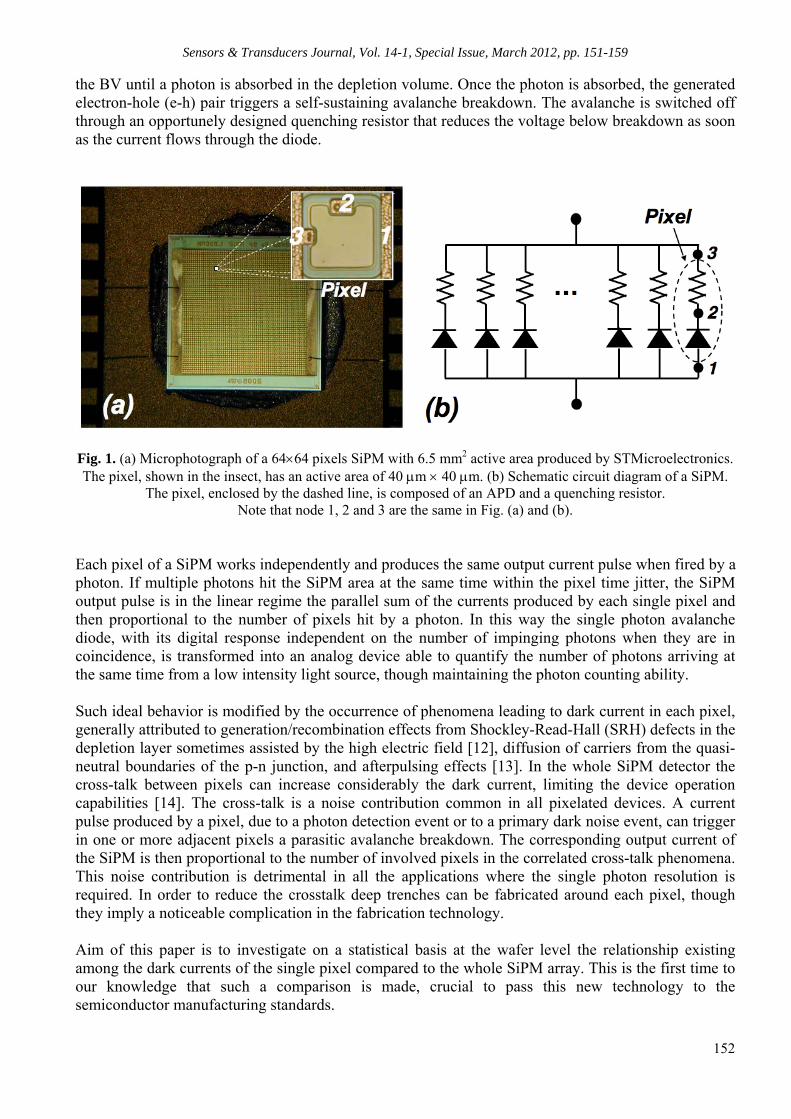
Received: 15 November 2011 /Accepted: 20 December 2011 /Published: 12 March 2012 Abstract: Aim of this paper is to investigate on a statistical basis at the wafer level the relationship existing among the dark currents of the single pixel compared to the whole Silicon Photomultiplier array. This is the first time to our knowledge that such a comparison is made, crucial to pass this new technology to the semiconductor manufacturing standards. In particular, emission microscopy measurements and current measurements allowed us to conclude that optical trenches strongly improve the device performances. Copyright © 2012 IFSA. Keywords: Silicon photomultipliers, Dark current, Wafer level. 1. Introduction Silicon-based single photon avalanche detectors [1-11] have been widely investigated since their appearance thanks to their interesting features: reduced dimensions, low weight, low fabrication costs, insensitivity to magnetic fields, and low operation voltage. Starting from single diode devices, progress in the field has driven the microelectronic industry to go towards designing and fabricating arrays of such devices, that is, avalanche diodes with an integrated quenching resistor connected in parallel by a metal grid and operating in Geiger mode, referred to as Si PhotoMultipliers (SiPMs), to cover areas up to ≈10 mm2 per device (Fig. 1 (a) and (b)). The principle of operation of each single avalanche detector consists in a p-n junction biased above the breakdown voltage (BV). Thanks to the high quality substrate and fabrication technology (low defect concentration), it can remain quiescent above
Sensors & Transducers Journal, Vol. 14-1, Special Issue, March 2012, pp. 151-159
152
the BV until a photon is absorbed in the depletion volume. Once the photon is absorbed, the generated electron-hole (e-h) pair triggers a self-sustaining avalanche breakdown. The avalanche is switched off through an opportunely designed quenching resistor that reduces the voltage below breakdown as soon as the current flows through the diode.
Fig. 1. (a) Microphotograph of a 6464 pixels SiPM with 6.5 mm2 active area produced by STMicroelectronics. The pixel, shown in the insect, has an active area of 40 m 40 m. (b) Schematic circuit diagram of a SiPM.
The pixel, enclosed by the dashed line, is composed of an APD and a quenching resistor. Note that node 1, 2 and 3 are the same in Fig. (a) and (b).
Each pixel of a SiPM works independently and produces the same output current pulse when fired by a photon. If multiple photons hit the SiPM area at the same time within the pixel time jitter, the SiPM output pulse is in the linear regime the parallel sum of the currents produced by each single pixel and then proportional to the number of pixels hit by a photon. In this way the single photon avalanche diode, with its digital response independent on the number of impinging photons when they are in coincidence, is transformed into an analog device able to quantify the number of photons arriving at the same time from a low intensity light source, though maintaining the photon counting ability. Such ideal behavior is modified by the occurrence of phenomena leading to dark current in each pixel, generally attributed to generation/recombination effects from Shockley-Read-Hall (SRH) defects in the depletion layer sometimes assisted by the high electric field [12], diffusion of carriers from the quasi-neutral boundaries of the p-n junction, and afterpulsing effects [13]. In the whole SiPM detector the cross-talk between pixels can increase considerably the dark current, limiting the device operation capabilities [14]. The cross-talk is a noise contribution common in all pixelated devices. A current pulse produced by a pixel, due to a photon detection event or to a primary dark noise event, can trigger in one or more adjacent pixels a parasitic avalanche breakdown. The corresponding output current of the SiPM is then proportional to the number of involved pixels in the correlated cross-talk phenomena. This noise contribution is detrimental in all the applications where the single photon resolution is required. In order to reduce the crosstalk deep trenches can be fabricated around each pixel, though they imply a noticeable complication in the fabrication technology. Aim of this paper is to investigate on a statistical basis at the wafer level the relationship existing among the dark currents of the single pixel compared to the whole SiPM array. This is the first time to our knowledge that such a comparison is made, crucial to pass this new technology to the semiconductor manufacturing standards.
Sensors & Transducers Journal, Vol. 14-1, Special Issue, March 2012, pp. 151-159
153
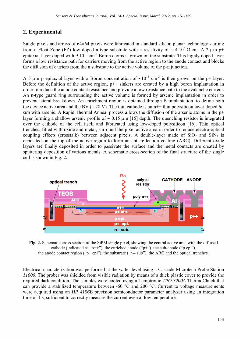
2. Experimental Single pixels and arrays of 6464 pixels were fabricated in standard silicon planar technology starting from a Float Zone (FZ) low doped n-type substrate with a resistivity of 4103 cm. A 2 m p+ epitaxial layer doped with 91016 cm-3 Boron atoms is grown on the substrate. This highly doped layer forms a low resistance path for carriers moving from the active region to the anode contact and blocks the diffusion of carriers from the n substrate to the active volume of the p-n junction. A 5 m p epitaxial layer with a Boron concentration of 1015 cm-3 is then grown on the p+ layer. Before the definition of the active region, p++ sinkers are created by a high boron implantation in order to reduce the anode contact resistance and provide a low resistance path to the avalanche current. An n-type guard ring surrounding the active volume is formed by arsenic implantation in order to prevent lateral breakdown. An enrichment region is obtained through B implantation, to define both the device active area and the BV ( 28 V). The thin cathode is an n++ thin polysilicon layer doped in-situ with arsenic. A Rapid Thermal Anneal process allows the diffusion of the arsenic atoms in the p+ layer forming a shallow arsenic profile of 0.15 m [15] depth. The quenching resistor is integrated over the cathode of the cell itself and fabricated using low-doped polysilicon [16]. Thin optical trenches, filled with oxide and metal, surround the pixel active area in order to reduce electro-optical coupling effects (crosstalk) between adjacent pixels. A double-layer made of SiO2 and SiN3 is deposited on the top of the active region to form an anti-reflection coating (ARC). Different oxide layers are finally deposited in order to passivate the surface and the metal contacts are created by sputtering deposition of various metals. A schematic cross-section of the final structure of the single cell is shown in Fig. 2.
Fig. 2. Schematic cross section of the SiPM single pixel, showing the central active area with the diffused cathode (indicated as “n++”), the enriched anode (“p+”), the sub-anode (“p epi”),
the anode contact region (“p+ epi”), the substrate (“n-- sub”), the ARC and the optical trenches. Electrical characterization was performed at the wafer level using a Cascade Microtech Probe Station 11000. The prober was shielded from visible radiation by means of a thick plastic cover to provide the required dark condition. The samples were cooled using a Temptronic TPO 3200A ThermoChuck that can provide a stabilized temperature between -60 °C and 200 °C. Current to voltage measurements were acquired using an HP 4156B precision semiconductor parameter analyzer using an integration time of 1 s, sufficient to correctly measure the current even at low temperature.
Sensors & Transducers Journal, Vol. 14-1, Special Issue, March 2012, pp. 151-159
154
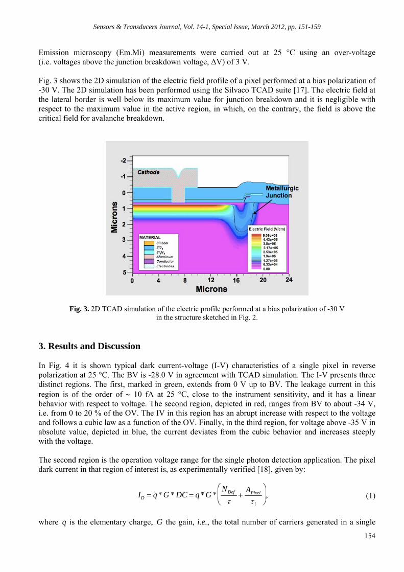
Emission microscopy (Em.Mi) measurements were carried out at 25 °C using an over-voltage (i.e. voltages above the junction breakdown voltage, ΔV) of 3 V. Fig. 3 shows the 2D simulation of the electric field profile of a pixel performed at a bias polarization of -30 V. The 2D simulation has been performed using the Silvaco TCAD suite [17]. The electric field at the lateral border is well below its maximum value for junction breakdown and it is negligible with respect to the maximum value in the active region, in which, on the contrary, the field is above the critical field for avalanche breakdown.
Fig. 3. 2D TCAD simulation of the electric profile performed at a bias polarization of -30 V in the structure sketched in Fig. 2.
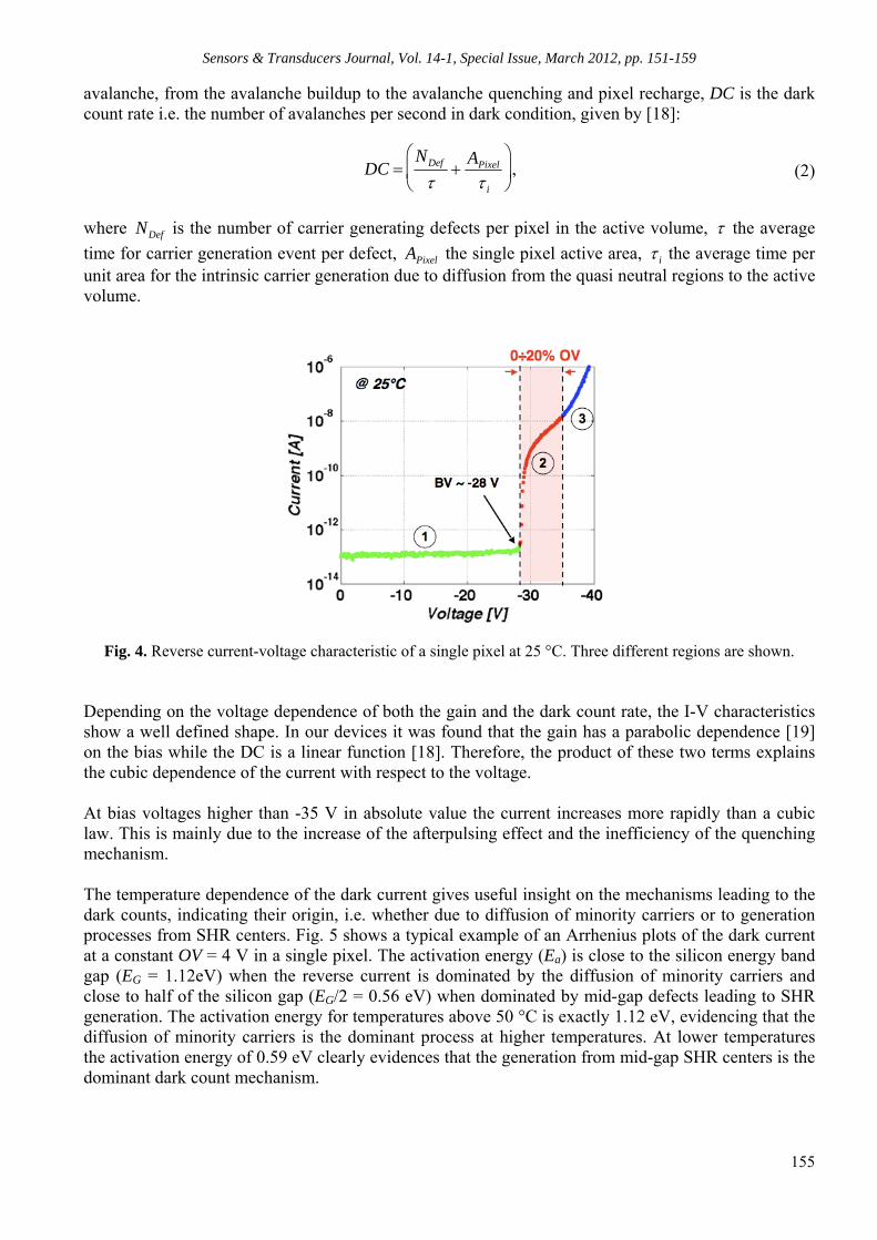
3. Results and Discussion In Fig. 4 it is shown typical dark current-voltage (I-V) characteristics of a single pixel in reverse polarization at 25 °C. The BV is -28.0 V in agreement with TCAD simulation. The I-V presents three distinct regions. The first, marked in green, extends from 0 V up to BV. The leakage current in this region is of the order of 10 fA at 25 °C, close to the instrument sensitivity, and it has a linear behavior with respect to voltage. The second region, depicted in red, ranges from BV to about -34 V, i.e. from 0 to 20 % of the OV. The IV in this region has an abrupt increase with respect to the voltage and follows a cubic law as a function of the OV. Finally, in the third region, for voltage above -35 V in absolute value, depicted in blue, the current deviates from the cubic behavior and increases steeply with the voltage. The second region is the operation voltage range for the single photon detection application. The pixel dark current in that region of interest is, as experimentally verified [18], given by:
ID q*G * DC q*G *NDef
APixel
i
, (1)
where q is the elementary charge, G the gain, i.e., the total number of carriers generated in a single
Sensors & Transducers Journal, Vol. 14-1, Special Issue, March 2012, pp. 151-159
155
avalanche, from the avalanche buildup to the avalanche quenching and pixel recharge, DC is the dark count rate i.e. the number of avalanches per second in dark condition, given by [18]:
DC NDef
APixel
i
, (2)
where NDef is the number of carrier generating defects per pixel in the active volume, the average
time for carrier generation event per defect, APixel the single pixel active area, i the average time per unit area for the intrinsic carrier generation due to diffusion from the quasi neutral regions to the active volume.
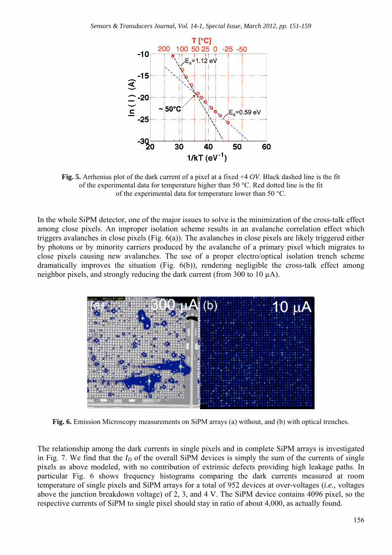
Fig. 4. Reverse current-voltage characteristic of a single pixel at 25 °C. Three different regions are shown. Depending on the voltage dependence of both the gain and the dark count rate, the I-V characteristics show a well defined shape. In our devices it was found that the gain has a parabolic dependence [19] on the bias while the DC is a linear function [18]. Therefore, the product of these two terms explains the cubic dependence of the current with respect to the voltage. At bias voltages higher than -35 V in absolute value the current increases more rapidly than a cubic law. This is mainly due to the increase of the afterpulsing effect and the inefficiency of the quenching mechanism. The temperature dependence of the dark current gives useful insight on the mechanisms leading to the dark counts, indicating their origin, i.e. whether due to diffusion of minority carriers or to generation processes from SHR centers. Fig. 5 shows a typical example of an Arrhenius plots of the dark current at a constant OV = 4 V in a single pixel. The activation energy (Ea) is close to the silicon energy band gap (EG = 1.12eV) when the reverse current is dominated by the diffusion of minority carriers and close to half of the silicon gap (EG/2 = 0.56 eV) when dominated by mid-gap defects leading to SHR generation. The activation energy for temperatures above 50 °C is exactly 1.12 eV, evidencing that the diffusion of minority carriers is the dominant process at higher temperatures. At lower temperatures the activation energy of 0.59 eV clearly evidences that the generation from mid-gap SHR centers is the dominant dark count mechanism.
Sensors & Transducers Journal, Vol. 14-1, Special Issue, March 2012, pp. 151-159
156
Fig. 5. Arrhenius plot of the dark current of a pixel at a fixed +4 OV. Black dashed line is the fit of the experimental data for temperature higher than 50 °C. Red dotted line is the fit
of the experimental data for temperature lower than 50 °C.
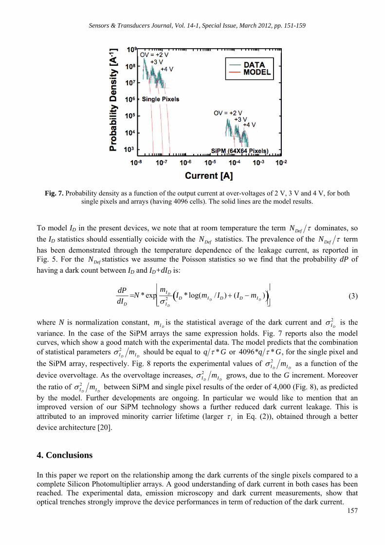
In the whole SiPM detector, one of the major issues to solve is the minimization of the cross-talk effect among close pixels. An improper isolation scheme results in an avalanche correlation effect which triggers avalanches in close pixels (Fig. 6(a)). The avalanches in close pixels are likely triggered either by photons or by minority carriers produced by the avalanche of a primary pixel which migrates to close pixels causing new avalanches. The use of a proper electro/optical isolation trench scheme dramatically improves the situation (Fig. 6(b)), rendering negligible the cross-talk effect among neighbor pixels, and strongly reducing the dark current (from 300 to 10 µA).
Fig. 6. Emission Microscopy measurements on SiPM arrays (a) without, and (b) with optical trenches. The relationship among the dark currents in single pixels and in complete SiPM arrays is investigated in Fig. 7. We find that the ID of the overall SiPM devices is simply the sum of the currents of single pixels as above modeled, with no contribution of extrinsic defects providing high leakage paths. In particular Fig. 6 shows frequency histograms comparing the dark currents measured at room temperature of single pixels and SiPM arrays for a total of 952 devices at over-voltages (i.e., voltages above the junction breakdown voltage) of 2, 3, and 4 V. The SiPM device contains 4096 pixel, so the respective currents of SiPM to single pixel should stay in ratio of about 4,000, as actually found.
Sensors & Transducers Journal, Vol. 14-1, Special Issue, March 2012, pp. 151-159
157
Fig. 7. Probability density as a function of the output current at over-voltages of 2 V, 3 V and 4 V, for both single pixels and arrays (having 4096 cells). The solid lines are the model results.
To model ID in the present devices, we note that at room temperature the term NDef dominates, so
the ID statistics should essentially coicide with the NDef statistics. The prevalence of the NDef term
has been demonstrated through the temperature dependence of the leakage current, as reported in Fig. 5. For the NDef statistics we assume the Poisson statistics so we find that the probability dP of
having a dark count between ID and ID+dID is:
dP
dID
N * expmI D
I D
2 ID * log(mI D/ID ) (ID mI D
)
(3)
where N is normalization constant, mI D
is the statistical average of the dark current and I D
2 is the
variance. In the case of the SiPM arrays the same expression holds. Fig. 7 reports also the model curves, which show a good match with the experimental data. The model predicts that the combination of statistical parameters I D
2 mI D should be equal to q *G or 4096*q * G, for the single pixel and
the SiPM array, respectively. Fig. 8 reports the experimental values of I D
2 mI D as a function of the
device overvoltage. As the overvoltage increases, I D
2 mI D grows, due to the G increment. Moreover
the ratio of I D
2 mI D between SiPM and single pixel results of the order of 4,000 (Fig. 8), as predicted
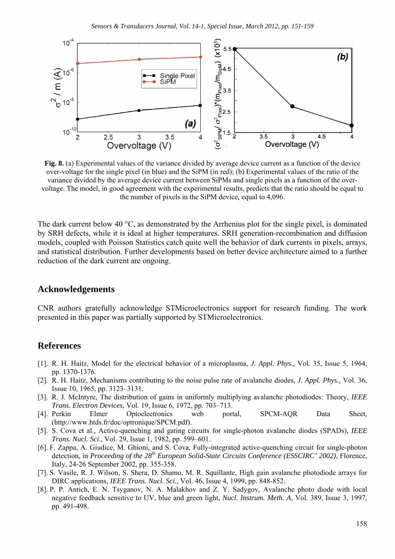
by the model. Further developments are ongoing. In particular we would like to mention that an improved version of our SiPM technology shows a further reduced dark current leakage. This is attributed to an improved minority carrier lifetime (larger i in Eq. (2)), obtained through a better
device architecture [20]. 4. Conclusions In this paper we report on the relationship among the dark currents of the single pixels compared to a complete Silicon Photomultiplier arrays. A good understanding of dark current in both cases has been reached. The experimental data, emission microscopy and dark current measurements, show that optical trenches strongly improve the device performances in term of reduction of the dark current.
Sensors & Transducers Journal, Vol. 14-1, Special Issue, March 2012, pp. 151-159
158
Fig. 8. (a) Experimental values of the variance divided by average device current as a function of the device over-voltage for the single pixel (in blue) and the SiPM (in red); (b) Experimental values of the ratio of the variance divided by the average device current between SiPMs and single pixels as a function of the over-
voltage. The model, in good agreement with the experimental results, predicts that the ratio should be equal to the number of pixels in the SiPM device, equal to 4,096.
The dark current below 40 °C, as demonstrated by the Arrhenius plot for the single pixel, is dominated by SRH defects, while it is ideal at higher temperatures. SRH generation-recombination and diffusion models, coupled with Poisson Statistics catch quite well the behavior of dark currents in pixels, arrays, and statistical distribution. Further developments based on better device architecture aimed to a further reduction of the dark current are ongoing. Acknowledgements CNR authors gratefully acknowledge STMicroelectronics support for research funding. The work presented in this paper was partially supported by STMicroelectronics. References [1]. R. H. Haitz, Model for the electrical behavior of a microplasma, J. Appl. Phys., Vol. 35, Issue 5, 1964,
pp. 1370-1376. [2]. R. H. Haitz, Mechanisms contributing to the noise pulse rate of avalanche diodes, J. Appl. Phys., Vol. 36,
Issue 10, 1965, pp. 3123–3131. [3]. R. J. McIntyre, The distribution of gains in uniformly multiplying avalanche photodiodes: Theory, IEEE
Trans. Electron Devices, Vol. 19, Issue 6, 1972, pp. 703–713. [4]. Perkin Elmer Optoelectronics web portal, SPCM-AQR Data Sheet,
(http://www.htds.fr/doc/optronique/SPCM.pdf). [5]. S. Cova et al., Active-quenching and gating circuits for single-photon avalanche diodes (SPADs), IEEE
Trans. Nucl. Sci., Vol. 29, Issue 1, 1982, pp. 599–601. [6]. F. Zappa, A. Giudice, M. Ghioni, and S. Cova, Fully-integrated active-quenching circuit for single-photon
detection, in Proceeding of the 28th European Solid-State Circuits Conference (ESSCIRC’ 2002), Florence, Italy, 24-26 September 2002, pp. 355-358.
[7]. S. Vasile, R. J. Wilson, S. Shera, D. Shamo, M. R. Squillante, High gain avalanche photodiode arrays for DIRC applications, IEEE Trans. Nucl. Sci., Vol. 46, Issue 4, 1999, pp. 848-852.
[8]. P. P. Antich, E. N. Tsyganov, N. A. Malakhov and Z. Y. Sadygov, Avalanche photo diode with local negative feedback sensitive to UV, blue and green light, Nucl. Instrum. Meth. A, Vol. 389, Issue 3, 1997, pp. 491-498.
Sensors & Transducers Journal, Vol. 14-1, Special Issue, March 2012, pp. 151-159
159
[9]. G. Bondarenko, P. Buzhan, B. Dolgoshein, V. Golovin, E. Guschin, A. Ilyin, V. Kaplin, A. Karakash, R. Klanner, V. Pokachalov, E. Popova, K. Smirnov, Limited Geiger-mode microcell silicon photodiode: new results, Nucl. Instrum. Meth. A, Vol. 442, Issue 1-3, 2000, pp. 187-192.
[10]. V. Golovin, Avalanche Photodetector, Russian Agency for Patents and Trademarks, Patent No. RU 2142175, 1998.
[11]. Z. Sadygov, Avalanche Detector, Russian Agency for Patents and Trademarks, Patent No. RU 2102820 1998.
[12]. G. A. M. Hurkx, H. C. de Graatf, W. J. Kloosterman, and M. P. G. Knuvers, A new analytical diode model including tunneling and avalanche breakdown, IEEE Trans. Elect. Dev., Vol. 39, Issue 9, 1992, pp. 2090-2098.
[13]. S. Cova, A. Lacaita, and G. Ripamonti, Trapping Phenomena in Avalanche Photodiode in Nanosecond Scale, IEEE Elect. Dev. Lett., Vol. 12, Issue 12, 1991, 685-687.
[14]. SILVACO International web portal, (http://www.silvaco.com). [15]. P. Buzhan, B. Dolgoshein, A. Ilyin, V. Kaplin, S. Klemin, R. Mirzoyan, E. Popova, M. Teshima,
The cross-talk problem in SiPMs and their use as light sensors for imaging atmospheric Cherenkov telescopes, Nucl. Instrum. Meth. A, Vol. 610, Issue 1, 2009, pp. 131-134.
[16]. E. Sciacca et al., Silicon Planar Technology for Single-Photon Optical Detector, IEEE Trans. Electr. Dev., Vol. 50, Issue 4, 2003, pp. 918-925.
[17]. M. Mazzillo, G. Condorelli, A. Piazza, D. Sanfilippo, G. Valvo, B. Carbone, G. Fallica, S. Billotta, M. Belluso, G. Bonanno, A. Pappalardo, L. Cosentino, P. Finocchiaro, Single-photon avalanche photodiodes with integrated quenching resistor, Nucl. Instrum. Meth. A, Vol. 592, Issue 2, 2008, pp. 367-373.
[18]. R. Pagano, S. Lombardo, S. Libertino, G. Valvo, G. Condorelli, B. Carbone, D. N. Sanfilippo, and G. Fallica, Understanding dark current in pixels of silicon photomultipliers, in Proceeding of the 40th European Solid State Device Research Conference (ESSDERC’ 2010), Seville, Spain, 13-17 September 2010, pp. 265-268.
[19]. R. Pagano, S. Libertino, D. Corso, G. Valvo, D. Sanfilippo, G. Fallica, and S. Lombardo, Dark current in SiPM pixels: data and model, Submitted to IEEE Trans. Electr. Dev.
[20]. R. Pagano, S. Libertino, D. Corso, G. Valvo, D. Sanfilippo, G. Condorelli, M. Mazzillo, A. Piana, B. Carbone, G. Fallica and S. Lombardo, Improvement of the diffusive component of dark current in SiPM pixels, article in preparation.
___________________ 2012 Copyright ©, International Frequency Sensor Association (IFSA). All rights reserved. (http://www.sensorsportal.com)

Sensors & Transducers Journal
Guide for Contributors
Aims and Scope Sensors & Transducers Journal (ISSN 1726-5479) provides an advanced forum for the science and technology of physical, chemical sensors and biosensors. It publishes state-of-the-art reviews, regular research and application specific papers, short notes, letters to Editor and sensors related books reviews as well as academic, practical and commercial information of interest to its readership. Because of it is a peer reviewed international journal, papers rapidly published in Sensors & Transducers Journal will receive a very high publicity. The journal is published monthly as twelve issues per year by International Frequency Sensor Association (IFSA). In additional, some special sponsored and conference issues published annually. Sensors & Transducers Journal is indexed and abstracted very quickly by Chemical Abstracts, IndexCopernicus Journals Master List, Open J-Gate, Google Scholar, etc. Since 2011 the journal is covered and indexed (including a Scopus, Embase, Engineering Village and Reaxys) in Elsevier products. Topics Covered Contributions are invited on all aspects of research, development and application of the science and technology of sensors, transducers and sensor instrumentations. Topics include, but are not restricted to:
Physical, chemical and biosensors; Digital, frequency, period, duty-cycle, time interval, PWM, pulse number output sensors and
transducers; Theory, principles, effects, design, standardization and modeling; Smart sensors and systems; Sensor instrumentation; Virtual instruments; Sensors interfaces, buses and networks; Signal processing; Frequency (period, duty-cycle)-to-digital converters, ADC; Technologies and materials; Nanosensors; Microsystems; Applications.
Submission of papers Articles should be written in English. Authors are invited to submit by e-mail [email protected] 8-14 pages article (including abstract, illustrations (color or grayscale), photos and references) in both: MS Word (doc) and Acrobat (pdf) formats. Detailed preparation instructions, paper example and template of manuscript are available from the journal’s webpage: http://www.sensorsportal.com/HTML/DIGEST/Submition.htm Authors must follow the instructions strictly when submitting their manuscripts. Advertising Information Advertising orders and enquires may be sent to [email protected] Please download also our media kit: http://www.sensorsportal.com/DOWNLOADS/Media_Kit_2012.pdf