silver on silicon (111): surface structural transformations and trace contaminant...
TRANSCRIPT

SILVER ON SILICON (111): SURFACE STRUCTURAL TRANSFORMATIONS
AND TRACE CONTAMINANT EFFECTS AT SUBMONOLAYER COVERAGE
A Dissertation
Presented to the Faculty of the Graduate School
of Cornell University
in Partial Fulfillment of the Requirements for the Degree of
Doctor of Philosophy
by
Gary Navrotski
January 2007

© 2007 Gary Navrotski
ALL RIGHTS RESERVED

SILVER ON SILICON (111): SURFACE STRUCTURAL TRANSFORMATIONS
AND TRACE CONTAMINANT EFFECTS AT SUBMONOLAYER COVERAGE
Gary Navrotski, Ph.D.
Cornell University 2007
The structural details for the formation of the (√3x√3)R30° Silver on Silicon
(111) system have eluded definitive resolution for 40 years. Wildly conflicting
evidence, gathered by every available surface science technique and theoretical
method, is beyond the scale customary for this field. In order for this system to
progress, a comprehensive review of the state-of-the-field, a newly constructed surface
structure diagram, a new set of experimentally determined atomic positions and the
quantitative effects minor contaminants are presented for Ag/Si(111).
From careful data mining and analysis of the nearly 600 papers in the literature
database, a comprehensive Ag-(√3x√3)R30°/Si(111) surface structure diagram has
been constructed. It includes a new β-(√3x√3)R30° phase; a two atom per unit cell
proto-cluster variation of the SAV structure, and also a γ-(√3x√3)R30° phase; with
structure similar to a later variant of the HCT model.
Atomic positions for Ag in the (√3x√3)R30° and the (3x1) structural
conformations have been determined by a number of complementary techniques; X-
ray Standing Wave (XSW), Surface Extended X-ray Absorption Fine Structure
(SEXAFS), Auger Electron Spectroscopy (AES), Rutherford Backscattering
Spectroscopy (RBS), Low Energy Electron Diffraction (LEED) and Isothermal
Desorption Spectroscopy (ITDS).

Three “second order” influences were also evaluated; boron, surface steps and
carbon. It was found that boron contamination and low surface steps densities have
insignificant influences on the √3 or (3x1) structures. Minor carbon contamination,
however, caused dramatic effects. First, tenth ML levels of carbon completely inhibit
the formation of the Ag-(3x1)/Si(111) phase. Second, at low C contamination levels,
the Ag-(√3x√3)R30° layer is comprised of dual, Ag-Si bond lengths (2.2Å and 2.6Å);
Ag-Ag bond lengths of 3.2Å; and Ag locations 0.97Å below the extension of bulk
Si(111) planes inferring a Si surface contraction of 0.2Å. Finally, carbon promoted a
high degree of Ag surface order and surface relaxation.
The existence of the β-(√3x√3)R30° and γ-(√3x√3)R30° phases is fully
consistent with quantitative literature citations and helps explain the decades-long
debate over model and critical coverage inconsistencies. The profound influence of C,
a ubiquitous contaminant in even the best experimental systems, helps explain surface
position, relaxation and coverage discrepancies.

iii
BIOGRAPHICAL SKETCH
Gary Navrotski was born on July 4, 1954 in Canonsburg, Pennsylvania to
Edwin Joseph Navrotski and Cecelia Bober Navrotski. He graduated from
Canon-McMillan Senior High School there in 1972. His undergraduate training in
physics was completed at Case Institute of Technology of Case Western Reserve
University with a B.S. in 1976. In 1978, he completed an M.S. degree in Materials
Science specializing in the area of high temperature creep of metallic materials, while
working at NASA Langley Research Center through the Joint Institute for the
Advancement of Flight Sciences (JIAFS) and George Washington University. He
spent four years as a staff scientist working on surface chemistry and aluminum alloy
development then three years as a senior scientist working on superplasticity and
fatigue research at Reynolds Metals Company, Corporate Research and Development
labs in Richmond, Virginia while earning his Professional Engineer's license in
Materials Engineering in 1982. Marrying the former Sarah Ellen Simonson in April
1984, he then returned for doctoral study in Materials Science at Cornell University in
September of 1985. During their time at Cornell, they were blessed with two children,
Alexander Edwin and Emily Irene. While compiling and analyzing the data presented
here, he worked as a freelance engineer and then, in late 1994, was employed by the
University of Chicago as the Project Engineer for x-ray optics, facilities and beamline
design for the BioCARS sector located at the Advanced Photon Source near Chicago,
Illinois. He returned to private engineering practice in 2003 where completed the
remainder of the compilation, analysis and writing of this dissertation.

iv
to
Sarah, Alex and Emily

v
ACKNOWLEDGMENTS
I would like to sincerely thank Professor J.M. Blakely for his extended service
as my thesis advisor and the chairman of my special committee. Professors B.W.
Batterman, S.L. Sass and J.D. Brock are gratefully acknowledged for serving as
members of my special committee. The guidance of Professor H.H. Johnson, a
member of my special committee before his death, is also gratefully acknowledged. I
would like to thank fellow students Mary LaPeyre Keeffe, Kit Umbach, Jun Liu, Jae
Pill Chang, and Bob McClelland for listening to and offering suggestions for my
research project. Also, the staff at CHESS, Lonny Berman of NSLS and particularly
Michael Bedzyk now at Northwestern University and Qun Shen at CHESS are
acknowledged for the use of their software, equipment and expertise. I would also like
to tell my wife, Sarah, how much her support and understanding during these many
‛‛lean years’’ have been. I could never have finished without her strength and devotion
not only to me but to our children Alex and Emily.
The experimental portion of this research was supported by the MRL Program
of the National Science Foundation and made use of MRL Central Facilities under
Award No. DMR-9121654. Data analysis, literature analysis, compilation and
composition portions were all privately funded. Allowances for liberal use of earned
personal leave to complete the writing of this document by the University of Chicago
is tacitly acknowledged.

vi
TABLE OF CONTENTS LIST OF FIGURES............................................................................................................ix LIST OF TABLES ...........................................................................................................xvi LIST OF ACRONYMS...................................................................................................xvii
Glossary of Surface Science Experimental Method Acronyms ..................................xvii Glossary of Surface Science Theoretical/Calculational Method Acronyms ................xix
CHAPTER ONE:.................................................................................................................1 Introduction .........................................................................................................................1
1.1 Preface .......................................................................................................................1 1.2 Historical Introduction to Silver on Silicon(111) ......................................................3 1.3 Thesis Statement........................................................................................................6 1.4 Introduction to Experimental Methods......................................................................9 1.5 Conventions.............................................................................................................11 1.6 References – Chapter One .......................................................................................13
CHAPTER TWO:..............................................................................................................15 Literature Analysis ............................................................................................................15
2.1 Literature Compilation ............................................................................................15 2.1.1 Introduction ......................................................................................................15 2.1.2 Chronological listing ........................................................................................17 2.1.3 Instrumental technique listing ..........................................................................18 2.1.4 Theoretical/computational technique listing ....................................................25
2.2 Ag/Si(111) surface phase diagram reconstruction ..................................................27 2.2.1 Overview ..........................................................................................................27 2.2.2 Low coverage, low temperature region ............................................................28 2.2.3 High coverage, low temperature region ...........................................................31 2.2.4 Low coverage, high temperature region...........................................................34 2.2.5 High coverage, high temperature region ..........................................................38 2.2.6 Special case: deposition on Si(111)-(2x1)........................................................39 2.2.7 Special case: over-deposition onto existing Ag-(√3x√3)R30°/Si(111)............43
2.3 Critical surface coverage determination for Ag-(√3x√3)R30° /Si(111)..................46 2.4 Surface model determination for Ag-(√3x√3)R30° /Si(111) ..................................52
2.4.1 Ag independent models, ...................................................................................53 2.4.2 Ag embedded models .......................................................................................54 2.4.3 Ag on top models..............................................................................................56 2.4.4 Critical model parameters.................................................................................69
2.5 Conclusion...............................................................................................................72 2.6 References – Chapter Two: a chronological record of Ag/Si(111) publications ....74 Addendum 1: Ag/Si(111) research expenditure estimate...........................................126

vii
CHAPTER THREE:........................................................................................................127 Theoretical Background ..................................................................................................127
3.1 X-Ray Standing Waves (XSW).............................................................................127 3.2 Surface Extended X-Ray Absorption Fine Structure (SEXAFS)..........................139
3.2.1 Introduction ....................................................................................................139 3.2.2 Basic EXAFS physics.....................................................................................139 3.2.3 Assumptions and corrections to the basic EXAFS physics............................142 3.2.4 SEXAFS Analysis Procedures .......................................................................143
3.3 Quantitative Auger Electron Spectroscopy (AES) ................................................152 3.3.1 Quartz oscillator crystal measurements..........................................................154 3.3.2 AES standards and sensitivity factor methods ...............................................154 3.3.3 AES first principles calculations ....................................................................155
3.4 Rutherford Backscattering Spectroscopy (RBS) ...................................................160 3.5 References -Chapter Three ....................................................................................164
CHAPTER FOUR: ..........................................................................................................172 Experimental Methods.....................................................................................................172
4.1 Ultra-high Vacuum System ...................................................................................172 4.2 Samples and Sample Preparation ..........................................................................176 4.3 X-ray Beamline, Optics and Beam Characteristics ...............................................183 4.4 Ancillary Experimental Apparatus ........................................................................186 4.5 References - Chapter Four.....................................................................................187
Chapter FIVE: .................................................................................................................188 Experimental Results and Analysis .................................................................................188
5.1 Ag Coverage Quantitation.....................................................................................188 5.1.1 Literature database..........................................................................................188 5.1.2 AES/RBS quantitation calibrations ................................................................191 5.1.3 AES results and RBS correlation ...................................................................193
5.2 XSW Positional Calculations ................................................................................193 5.2.1 Node-S testing: C free, B exposed, Flat Si(111) ............................................196 5.2.2 Node-T testing: C exposed, B exposed, Flat Si(111) .....................................205 5.2.3 Node-U testing: C exposed, B free, Flat Si(111)............................................207 5.2.4 Node-V testing: C free, B free, Flat Si(111) ..................................................209 5.2.5 Node-W testing: C free, B exposed, 0.5° miscut Si(111)...............................211 5.2.6 Node-X and Y testing: (XSW not done) ........................................................218 5.2.7 Node-Z testing: C free, B free, 0.5° miscut Si(111).......................................218 5.2.8 Testing of Ag-√3 structures at atmospheric pressures....................................223 5.2.9 Summary of XSW results ...............................................................................228
5.3 SEXAFS Bond Length Measurements ..................................................................229 5.3.1 Node-S testing: C free, B exposed, Flat Si(111) ............................................231 5.3.2 Node-T testing: C exposed, B exposed, Flat Si(111) .....................................234 5.3.3 Node-U testing (No SEXAFS testing done)...................................................237 5.3.4 Node-V testing: C free, B free, Flat Si(111) ..................................................237

viii
5.3.5 Node-W testing: C free, B exposed, 0.5° miscut Si(111)...............................240 5.3.6 Node-X and Y testing: (SEXAFS not done) ..................................................243 5.3.6 Node-X and Y testing: (SEXAFS not done) ..................................................243 5.3.7 Node-Z testing: C free, B free, 0.5° miscut Si(111).......................................243 5.3.8 Summary of SEXAFS results .........................................................................247
5.4 References - Chapter Five .....................................................................................249 CHAPTER SIX: ..............................................................................................................251 Summary and Conclusions ..............................................................................................251
6.1 Summary Compilation of Results .........................................................................251 6.1.1 Overview ........................................................................................................251 6.1.2 Boron Exposure ..............................................................................................253 6.1.3 Evaluation of the reduced test matrix .............................................................257 6.1.4 0.5° Vicinal Surface Effects ...........................................................................259 6.1.4 Carbon Effect..................................................................................................260 6.1.5 Surface Coverage / Surface Effect ................................................................261 6.1.6 Comparison to existing structural models ......................................................262
6.2 Conclusions ...........................................................................................................264

ix
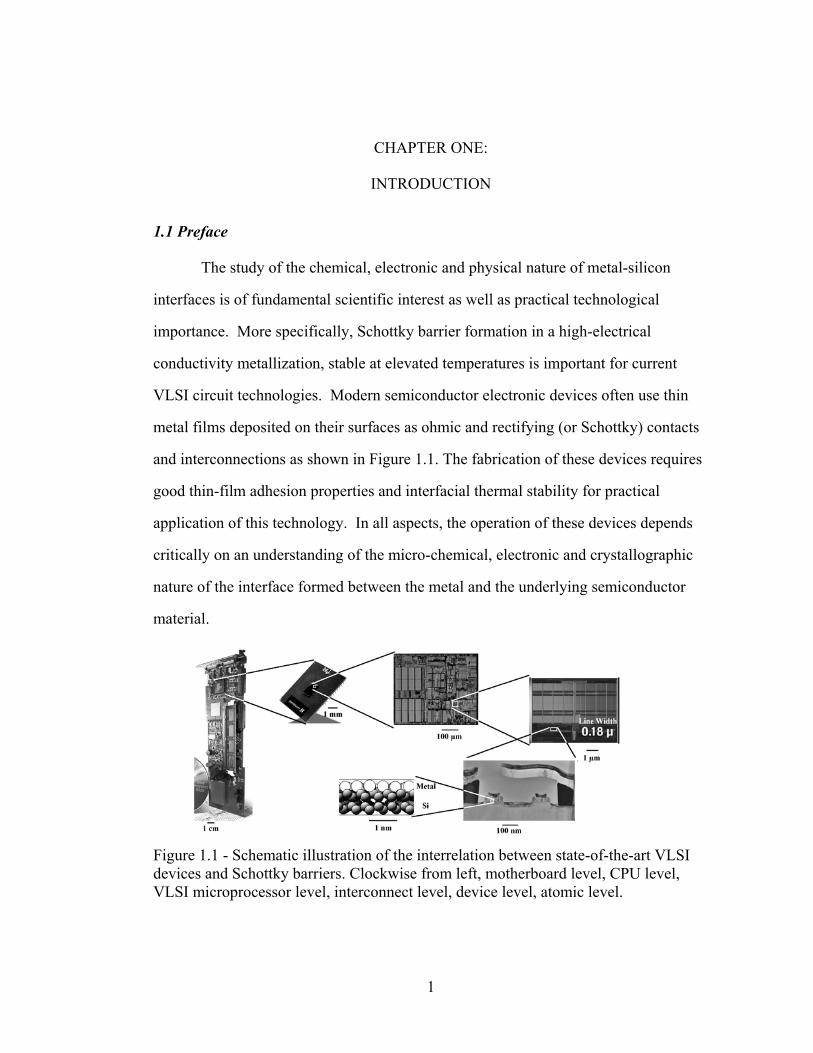
LIST OF FIGURES Figure 1.1 - Schematic illustration of the interrelation between state-of-the-art VLSI
devices and Schottky barriers. Clockwise from left, motherboard level, CPU level, VLSI microprocessor level, interconnect level, device level, atomic level.......1
Figure 1.2 - B/Si(111)-(√3x√3)R30° structure. (After Headrick, ) .....................................7 Figure 1.3 - Schematic illustration of coherent interfering wave fronts producing a
movable standing wave pattern. ................................................................................10 Figure 2.1 - Annual and cumulative Ag/Si(111) publication history................................16 Figure 2.2 - Distribution of Ag/Si(111) papers by publication source..............................16 Figure 2.3 - Idealized surface structure diagram for Ag/Si(111). .....................................27 Figure 2.4 - Low coverage, low temperature quadrant of the Ag/Si(111)-(7x7) surface
structure diagram.......................................................................................................30 Figure 2.5 - High coverage, low temperature quadrant of the Ag/Si(111)-(7x7) surface
structure diagram.......................................................................................................33 Figure 2.6 - Low coverage, high temperature quadrant of the Ag/Si(111)-(7x7) surface
structure diagram.......................................................................................................35 Figure 2.7 - High coverage, high temperature quadrant of the Ag/Si(111)-(7x7) surface
structure diagram ......................................................................................................41 Figure 2.8 - Special case: surface structure diagram, Ag on cleaved Si(111)-(2x1).........42 Figure 2.9 - Special case: surface structure diagram, Ag on a pre-formed Ag-
(√3x√3)/Si(111) surface. ...........................................................................................45 Figure 2.10 - Historical trend; Ag-(√3x√3) phase critical surface coverage, θC. ..............46 Figure 2.11 - Null correlations; critical coverage vs. substrate type & dopant.
Provisional correlations; resistivity& surface temp. .................................................49 Figure 2.12 - Provisional correlation; critical coverage vs. Ag deposition source............50 Figure 2.13 - Correlation; critical coverage vs. experimental method ..............................51 Figure 2.14 - Ag-√3 model historical development timeline. ...........................................59 Figure 2.15 - Null correlation; model vs. substrate type. ..................................................60 Figure 2.16 - Null correlation; model vs. substrate dopant. ..............................................61 Figure 2.17 - Provisional correlation; model vs. substrate resistivity. ..............................64 Figure 2.18 - Null correlation; model vs. substrate preparation temperature....................65 Figure 2.19 - Provisional correlation; model vs. sample preparation temperature. .........66 Figure 2.20 - Provisional correlation; model vs. deposition source material. ...................67 Figure 2.21 - Correlation; model vs. experimental method...............................................68 Figure 2.22 - Left: ideal surface cross section. Right: exact HCT-6 model with bulk
rearrangement, surface contraction & adlayers. ........................................................71 Figure 3.1 - X-ray Standing Wave (XSW) formation by coherent interference between
incident and outgoing X-ray plane waves. ..............................................................127 Figure 3.2 - A) Prototype Ag/Si(111) surface. B) Incident X-Ray plane-wave not yet
in the Bragg diffraction condition. Incident wavevector, ko, and transmitted wavevector, kt. Ag AES (Auger Electron), Pe- (photoelectron production) and

x
Flu. (fluorescence) proportional to Ag atom density. C) Just entering diffraction condition. AES, Pe- and Flu. decreasing due to destructive interference................131
Figure 3.2 - D) Dynamical diffraction fully formed. An X-ray Standing Wave field has been generated, “low angle” side, with periodicity D, equal to dSi(111) and nodes (no E field intensity) at the positions of the diffracting planes thus no Ag fluorescence. E) XSW field at the “high angle” side of the diffraction. The field has moved inward by ½dSi(111) due to the π phase shift between ko and kR. Fluorescence = 4X the off Bragg. F) Out of diffraction, high angle side................132
Figure 3.3 - Calculated fluorescence curves for a perfectly coherent assemblage of atoms at different coherent positions, Fc excited by an XSW field. .......................133
Figure 3.4 A-E (see text): Examples of atomic arrangements of Ag (filled circles) on Si(111) (open circles) that would give the same coherent position, Φc=1, and coherent fraction, Fc=1, from a Si(111) X-ray Standing Wave experiment series. 137
Figure 3.5 A-E (see text): Examples of the effect of atomic arrangements of Ag (filled circles) on Si(111) (open circles) that alter the coherent fraction parameter, Fc. ...138
Figure 3.6 - Schematic illustration of an outgoing electron wavefunction, ψ1, interfering with coherent wavefunction ψf backscattered from four near neighbors. ................................................................................................................140
Figure 3.7a - Raw absorption data, 25 micron Ag foil ....................................................147 Figure 3.7b - Absorption spectrum, background removed, normalized to electron
kinetic energy zero-point, Eo at edge jump inflection. ............................................147 Figure 3.7c - Spline fit to remove "free atom" contribution to the XFS oscillations ......148 Figure 3.7d - The "Chi Function", χ(k ) ..........................................................................148 Figure 3.7e - k weighted wavefunction ...........................................................................149 Figure 3.7f - Fourier transformed "1st approximation" radial distribution function with
Hanning isolation window function. .......................................................................149 Figure 3.7g – Back-transformation of the filtered radial distribution function showing
amplitude envelope and oscillatory components.....................................................150 Figure 3.7h - Phase matching to known reference standard............................................150 Figure 3.7i - Back-transformation of filtered and phase adjusted wavefunction
showing real (solid) and imaginary (dashed) components of the Fourier transformation..........................................................................................................151
Figure 3.7j - Final single-pair radial distribution function solved, dN-N = 2.878 Å.........151 Figure 3.8 - CMA measured Auger electron spectra for Si, Ag and C. (After Davis)
Ag MNN peaks identified by Housley, Heckingbottom and Todd and Si LVV peaks in LeLay notation where V2 represents a lower 3s-like final state and V4 indicates an 3p-like final state. ................................................................................153
Figure 3.9 - Schematic of RBS analysis of Ag/Si(111). A 2.7 MeV He++ ion with initial kinetic energy and momentum recoils elastically after collision with a surface atom.............................................................................................................160
Figure 4.1 - Experimental vacuum system in place at CHESS D-line. Left, photo showing spherical vacuum chamber and pumping well outfitted with: 1) stepping motor manipulator control, 2) manipulator, 3) upper TSP, 4) CMA, 5) ion source, 6) RGA, 7) 200 l/s pumping well, 8) rotation/translation base, 9) final x-

xi
ray slit, 10) x-ray flight tube, 11) Be entrance window, 12) Si(Li) fluorescence detector and 13) surface science instrumentation control electronics. ....................173
Figure 4.2 - Cross-section of experimental UHV chamber, in plane of incident X-rays. Surface analytical instrumentation and their respective foci are shown. ................174
Figure 4.3- a) (111) pole figure for the diamond cubic structure; b) Laue photograph of 0° flat surface sample wafer; c) 0.5° vicinally cut sample wafer. ...........................178
Figure 4.4 - Schematic illustration of CHESS D-line synchrotron radiation line, Si(111) monochromator and UHV experimental system ........................................183
Figure 4.5 - Schematic illustration of Si(111) and (220) monochromators in limit design configurations...............................................................................................185
Figure 5.1 - Compilation of literature Auger vs Coverage calibrations for room temperature deposits of Ag on Si(111)....................................................................189
Figure 5.2 - Compilation of literature Auger vs Coverage calibrations for elevated temperature deposits of Ag on Si(111)....................................................................190
Figure 5.3 - Determination of fitting procedure and He++ dose (sputtering) effects on submonolayer Ag/Si(111) coverage calibrations. Terms “Gross Thick”, “Net Thick” and “Best Fit” refer to fitting procedures fitting total RBS backscattered count (Signal and noise), RBS backscattered count in a small region and a PERT or best fit using background subtraction and instrumental variability parameters respectively..............................................................................................................191
Figure 5.4 - Experimental determinations of Auger vs Coverage calibration by various AES quantitation methods and by RBS direct quantitation. ...................................192
Figure 5.5 - Example Fluorescence Spectra. Complete spectra such as this, were recorded for each of 32 points along the Darwin reflectivity curve during the XSW experimental scans.........................................................................................194
Figure 5.6- Statistical Experimental Design screening test matrix used for the study of minor variables on the structure of Ag/Si(111) .......................................................196
Figure 5.7a - Path-dependant XSW measurement locations. Open circles depict coverage and temperatures of XSW measurements of Figure 5.7b and 5.8a, b, c respectively (see text). Coverage range on data taken at 560°C is due to ongoing Ag desorption at that temperature. ..........................................................................197
Figure 5.7b - XSW results, Node S testing, 2.58 ML Ag/Si(111). Top curve, fluorescent yield, symbols and error bars and theoretical fit. Bottom symbols and curve, measured and fit reflectivity. Φc =0.79.........................................................199
Figure 5.7c - Node S testing. Possible locations (Ag1 , Ag2 or combination) for Ag relative to Si(111) diffraction planes. ......................................................................200
Figure 5.8a - XSW position, Node S testing, ~0.9 ML, 560° C (Beginning of desorption and 3x1 formation). √3x√3R30° Ag/Si(111) only, Φc =0.78 ................201
Figure 5.8b - XSW position, Node S testing, ~0.5 ML, 560° C (Middle of desorption and 3x1 formation process). √3x√3R30° + 3x1 Ag/Si(111), Φc =0.78...................202
Figure 5.8c - XSW position, Node S testing, ~0.1 ML, 560° C (End of desorption of 3x1 phase), 3x1 Ag/Si(111), Φc =0.79 ....................................................................203
Figure 5.9 - XSW results, Node S testing, 0.82 ML Ag/Si(111) at 250°C. Top curve, fluorescent yield, symbols and error bars and theoretical fit. Bottom symbols and curve, measured and fit reflectivity. .......................................................................204

xii
Figure 5.10a - Path-dependant XSW measurement, Node T testing. Open circle shows coverage and temperature of sample preparation and measurement reported in Figure 5.10b.............................................................................................................205
Figure 5.10b - XSW Results, Node T testing, 0.13 ML Ag/Si(111). Top curve, fluorescent yield, measured values, error bars and theoretical fit. Bottom symbols and curve, measured values and theoretical fit to reflectivity. ................................206
Figure 5.11a - Path-dependant XSW measurement, Node U testing. Open circle shows coverage and temperature of sample preparation and measurement reported in Figure 5.11b ..........................................................................................207
Figure 5.11b - XSW Results, Node U testing, 0.11 ML Ag/Si(111). Top curve, fluorescent yield, measured values, error bars and theoretical fit. Bottom symbols and curve, measured reflectivity..............................................................................208
Figure 5.12a - Path-dependant XSW measurement, Node V testing. Open circle shows coverage and temperature of sample preparation and measurement reported in Figure 5.12b ..........................................................................................209
Figure 5.12b - XSW Results, Node V testing, 0.5 ML Ag/Si(111). Top curve, fluorescent yield, measured values, error bars and theoretical fit. Bottom symbols and curve, measured values and theoretical fit to reflectivity. Insufficient data for meaningful statistical fits. Dashed theoretical fits are intended as baseline references.................................................................................................................210
Figure 5.13a - Path-dependant XSW measurement, Node W testing. Open circle shows coverage and temperature of sample preparation and measurement reported in Figure 5.13b, c, d, e, f ...........................................................................212
Figure 5.13b - XSW Results, Node W testing, 0.2 ML Ag/Si(111), 400°C. Top curve, fluorescent yield, measured values, error bars and theoretical fit. Bottom symbols and curve, measured values and theoretical fit to reflectivity. ................................213
Figure 5.13c - XSW Results, Node W testing, 0.2 ML Ag/Si(111), 30°C. Top curve, fluorescent yield, measured values, error bars and theoretical fit. Bottom symbols and curve, measured values and theoretical fit to reflectivity .................................214
Figure 5.13d - XSW Results, Node W testing, 0.2 ML Ag/Si(111), 500°C. Top curve, fluorescent yield, measured values, error bars and theoretical fit. Bottom symbols and curve, measured values and theoretical fit to reflectivity .................................215
Figure 5.13e - XSW Results, Node W testing, 0.2 ML Ag/Si(111), 550°C. Top curve, fluorescent yield, measured values, error bars and theoretical fit. Bottom symbols and curve, measured values and theoretical fit to reflectivity .................................216
Figure 5.13f - XSW Results, Node W testing, 0 ML Ag/Si(111), 550°C. (after desorption) Top curve, fluorescent yield, measured values, error bars and theoretical fit. Bottom symbols and curve, measured values and theoretical fit to reflectivity................................................................................................................217
Figure 5.14a - Path-dependant XSW measurement, Node Z testing. Open circles show coverage & temperature of sample preparation & testing.......................................218
Figure 5.14b - XSW Results, Node Z testing, 0.25 ML Ag/Si(111), 400°C. Top curve, fluorescent yield, measured values, error bars and theoretical fit. Bottom symbols and curve, measured values and theoretical fit to reflectivity .................................219

xiii
Figure 5.14c - XSW Results, Node Z testing, 0.25 ML Ag/Si(111), 400°C. Same conditions as 5.14b with changes in beam conditions. Top curve, fluorescent yield, measured values, error bars and theoretical fit. Bottom symbols and curve, measured values and theoretical fit to reflectivity Figure 5.14d - XSW Results, Node Z testing, 0.25 ML Ag/Si(111), 30°C. Top curve, fluorescent yield, measured values, error bars and theoretical fit. Bottom symbols and curve, measured values and theoretical fit to reflectivity...................................................220
Figure 5.14d - XSW Results, Node Z testing, 0.25 ML Ag/Si(111), 30°C. Top curve, fluorescent yield, measured values, error bars and theoretical fit. Bottom symbols and curve, measured values and theoretical fit to reflectivity .................................221
Figure 5.14e - XSW Results, Node Z testing, 0.25 ML Ag/Si(111), 500°C. Top curve, fluorescent yield, measured values, error bars and theoretical fit. Bottom symbols and curve, measured values and theoretical fit to reflectivity .................................222
Figure 5.15a - XSW Results, Post-mortem bench testing, 31.6 ML Ag/Si(111), R.T. Top curve, fluorescent yield, measured values, error bars and theoretical fit. Bottom symbols and curve, measured values and theoretical fit to reflectivity......224
Figure 5.15b - XSW Results, Post-mortem bench testing, 9.3 ML Ag/Si(111), R.T. Top curve, fluorescent yield, measured values, error bars and theoretical fit. Bottom symbols and curve, measured values and theoretical fit to reflectivity......225
Figure 5.15c - XSW Results, Post-mortem bench testing, 2.16 ML Ag/Si(111), R.T. Top curve, fluorescent yield, measured values, error bars and theoretical fit. Bottom symbols and curve, measured values and theoretical fit to reflectivity......226
Figure 5.15d - XSW Results, Post-mortem bench testing, 0.48 ML Ag/Si(111), R.T. Top curve, fluorescent yield, measured values, error bars and theoretical fit. Bottom symbols and curve, measured values and theoretical fit to reflectivity......227
Figure 5.16 - Effect of Compton modified radiation on S/N ratio of Ag/Si SEXAFS measurements ..........................................................................................................231
Figure 5.17a - Path dependant sample preparation, coverage and phase for Node-S SEXAFS measurements. Open circle depicts coverage and temperatures of measurements of Figure 5.17b ................................................................................232
Figure 5.17b - Node S SEXAFS measurement, 2.58 ML Ag/Si(111)- 400 °C (top) fluorescence signal, (middle) Chi function and fit from atom-pair shown in (bottom) radial distribution function with Hanning filter window..........................233
Figure 5.18a - Sample preparation, coverage and phase for Node-T SEXAFS measurements. Open circle depicts coverage and temperatures of duplicate measurements shown in Figure 5.18b and 5.18c.....................................................234
Figure 5.18b - Node T SEXAFS measurement, 0.12 ML Ag/Si(111)- 400 °C Wide slits (.5mm v x 5mm h) for large surface area averaging. Curves (top) fluorescence signal, (middle) Chi function and fit from atom-pair shown in (bottom) radial distribution function with Hanning filter window..........................235
Figure 5.18c - Node T SEXAFS measurement, 0.12 ML Ag/Si(111)- 400 °C Narrow slits (.5mm v x 1mm h) for small surface area averaging. Curves; (top) fluorescence signal, (middle) Chi function and fit from atom-pair shown in (bottom) radial distribution function with Hanning filter window..........................236

xiv
Figure 5.19a - Path-dependant SEXAFS measurement, Node V testing. Starting at 1.33 ML dose, sample preparation is shown by solid line. Open circle shows coverage and temperature of measurement reported in Figure 5.19b,c . ................237
Figure 5.19b - Node V SEXAFS measurement π polarization, 0.51 ML Ag/Si(111)- 400 °C (top) fluorescence signal, (middle) Chi function and fit from atom-pair shown in (bottom) radial distribution function with Hanning filter window ..........238
Figure 5.19c - Node V SEXAFS measurement σ polarization, 0.51 ML Ag/Si(111)- 400 °C (top) fluorescence signal, (middle) Chi function and fit from atom-pair shown in (bottom) radial distribution function with Hanning filter window ..........239
Figure 5.20a - Path-dependant SEXAFS measurement, Node W testing. Starting at 1.33 ML dose, sample preparation is shown by solid line. Open circle shows coverage and temperature of measurement reported in Figure 5.20b,c ..................240
Figure 5.20b - Node W SEXAFS measurement π polarization, 1.35 ML Ag/Si(111)- 400 °C (top) fluorescence signal, (middle) Chi function and fit from atom-pair shown in (bottom) radial distribution function with Hanning filter window ..........241
Figure 5.20c - Node W SEXAFS measurement σ polarization, 0.15 ML Ag/Si(111)- 400 °C (top) fluorescence signal, (middle) Chi function and fit from atom-pair shown in (bottom) radial distribution function with Hanning filter window ..........242
Figure 5.21a - Path-dependant SEXAFS measurement, Node Z testing. Starting at 0.6 ML dose, sample preparation is shown by solid line. Dashed line indicates structure and coverage change after 24 hour hold in UHV. Open circle shows coverage and temperature of measurement reported in Figure 5.21b,c and d.........243
Figure 5.21b - Node Z SEXAFS measurement π polarization, 0.25 ML Ag/Si(111)- 400 °C (top) fluorescence signal, (middle) Chi function and fit from atom-pair shown in (bottom) radial distribution function with Hanning filter window ..........244
Figure 5.21c - Node Z SEXAFS measurement π polarization, 0.1 ML Ag/Si(111)- 400 °C (top) fluorescence signal, (middle) Chi function and fit from atom-pair shown in (bottom) radial distribution function with Hanning filter window......................245
Figure 5.21d - Node Z SEXAFS measurement σ polarization, 0.1 ML Ag/Si(111)- 400 °C (top) fluorescence signal, (middle) Chi function and fit from atom-pair shown in (bottom) radial distribution function with Hanning filter window......................246
Figure 6. 1 - Completed nodes of the three-level statistical screening experiment design. (Half symbol at Nodes U and V indicate only XSW or SEXAFS results available respectively.) ............................................................................................251
Figure 6.2 - XSW measurement; effect of B exposure on nominal positions of 3x1 + √3x√3R30° Ag/Si(111) phases. Filled symbols, Node W (from Figure 5.13c). Open symbols, Node Z (from Figure 5.14d). Solid lines, theoretical fits to Rocking Curve and Coherent Position. ...................................................................255
Figure 6. 3 - XSW measurement; effect of B exposure on nominal positions of √3x√3R30° Ag/Si(111) phase. Filled symbols, Node T (from Figure 5.10b). Open symbols, Node U (from Figure 5.11b). Solid lines, theoretical fits to Rocking Curve and Coherent Position. ...................................................................256
Figure 6.4 - Reduced dimensionality test matrix removing Boron null test result..........257 Figure 6. 5 - Schematic model illustration of atomic arrangements in A) Node W or Z
Φc and bond lengths and B) Node T or U Φc and bond lengths. ..........................258

xv
Figure 6. 6 - Four layer model illustration of A) Takayanagi model of the Si(111) 7x7 surface and B) bulk-like Si(111) terminated surface...............................................259
Figure 6. 7 - Left: SAV class of models proposed as the β-Ag√3 form. Right: HCT class model proposed as the γ-Ag√3 form. (dark spheres: Si, white spheres: Ag, small diamond: Si(111) surface unit cell, large parallelogram: (√3x√3)R30°-Ag surface unit cell, disregard Ag sphere sizes, atomic radius used at left, covalent radius at right),.........................................................................................................266

xvi
LIST OF TABLES Table 2.1 - Ag/Si(111) Papers Categorized by Primary Experimental Technique ...........18 Table 2.2 - Ag/Si(111) Papers Categorized by Primary Theoretical Technique...............25 Table 2.3 - Summary of bond lengths and bulk registry for Ag/Si(111) models. .............70 Table 4.1 - Critical CHESS D-line Source and Beamline Component Values ...............184 Table 5.1 - Summary of XSW findings for Ag/Si(111) ..................................................228 Table 5.2 - Summary of SEXAFS findings for Ag/Si(111) ............................................248 Table 6.1: Summary of Sample Preparation, XSW and SEXAFS findings for
Ag/Si(111) ...............................................................................................................252 Table 6.2 - Summary comparison of experimental and surface model matches.............263

xvii
LIST OF ACRONYMS
Glossary of Surface Science Experimental Method Acronyms 2PPE Two-Photon PhotoEmission Spectroscopy AED (µAED) Auger Electron Diffraction (micro AED) AES (µAES) Auger Electron Spectroscopy (micro AES) AFM Atomic Force Microscopy AREELS Angular(ly) Resolved Electron Energy Loss Spectroscopy. AR-Imaging Angularly Resolved Imaging (with AR-Electron Spectroscopy) ARUPS Angle-Resolved Ultraviolet Photoelectron Spectroscopy ( = ARPES) ARPES Angle-Resolved Photo-Emission Spectroscopy ( = ARUPS) AST Auger Signal-Time (plots) b-SEI biased Secondary Electron Imaging BE Binding energy BIS Bremsstrahlung Isochromat Spectroscopy (=IPE, e- in/X-ray out) CAICISS Coaxial Impact Collision Ion Scattering Spectroscopy CL CathodoLuminescence CPD Contact Potential Difference (from SKPM) CTR Crystal Truncation Rod (X-ray surface diffraction) CV Cyclic Voltammetry DFT Density Functional Theory DOS Density of states DR Differential Reflectance ( = Photoreflectance) DRS DR Spectroscopy EDC Energy distribution curve EELS Electron-Energy-Loss Spectroscopy (=ELS) ELEED Elastic Low Energy Electron Diffraction ELS Electron-energy Loss Spectroscopy (=EELS) EMSS Electromigration on Semiconductor Surfaces ERDA Elastic Recoil Detection Analysis (= FRES) ESCA Electron Spectroscopy for Chemical Analysis (=XPS) ESD Electron Stimulated Desorption FE-SEM Field Emission (source) SEM FIM Field Ion Microscopy FRES Forward Recoil Elastic Spectrometry (= ERDA) FPC First Principles Calculations GIXD Grazing Incidence X-ray Diffraction GIXRD Grazing Incidence X-ray Diffraction GIXRF Grazing Incidence X-ray Fluorescence HR- High-Resolution (as in HREELS, HR-PES, HR-LEED ) ICB Ionized Cluster Beam ICISS Impact Collision Ion Scattering Spectroscopy IID Ion Impact Desorption

xviii
IPE Inverse Photoemission Current (=BIS, =UVIS) IPES Inverse Photoemission Spectroscopy ISS Ion scattering spectroscopy ITCS Isothermal Condensation Spectroscopy ITDS Isothermal Desorption Spectroscopy IV Intensity-Voltage (LEED) or Current-Voltage (electrical conductivity) KMC Kinetic Monte-Carlo calculations KRIPS K (momentum) Resolved Inverse Photoelectron (-emission) Spectroscopy LCAO Linear combination of atomic orbitals LDA Local Density Approximation (as in LDA-LDF or LDA-DFT theory) LDF Linear Density Functional theory (Band Structure Calculations) LEED Low-Energy Electron Diffraction LEED/CMTA LEED Constant Momentum Transfer Averaging LEEM Low Energy Electron Microscopy LEIS Low Energy Ion Scattering (Spectroscopy) LEISS LEIS Spectroscopy LNT Liquid-nitrogen temperature MC Monte-Carlo calculations MCS Monte-Carlo Simulations MD Molecular Dynamics (Simulations) MEED Medium Energy Electron Diffraction MEES Medium Energy quasi-Elastic Scattered electrons MEIS Medium Energy Ion Scattering MEISS MEIS Spectroscopy MSC Multiple Scattering Cluster calculations NC- Noncontact (as NC-AFM) NE- Near Edge (as NEXAFS = XANES) NRA Nuclear Reaction Analysis OSHG Optical Second Harmonic Generation PAX Photoemission of Adsorbed Xenon PED Photoelectron Diffraction PEEM Photoemission Electron Microscopy PES PhotoEmission Spectroscopy ( = UPS) Photoreflectance ( = DRS) PIXE Proton Induced X-Ray Emission PSD Photon Stimulated Desorption QKLEED Quasi-Kinematical LEED RBS Rutherford Back Scattering or Rutherford Backscattering Spectroscopy REM Reflection Electron Microscopy RHEED Reflection-High-Energy Electron Diffraction RHEED-TRAXS : RHEED Total Reflection Angle X-ray Spectroscopy RHEPD Reflection High-Energy Positron Diffraction RNRA Resonant Nuclear Reaction Analysis RT Room temperature

xix
SAM Scanning Auger Microscopy SBH Schottky Barrier Height SEE (angle scanned) Secondary Electron Emission SEM Scanning Electron Microscopy SEXAFS Surface Extended X-ray Absorption Fine Structure SHG Second Harmonic Generation SIMS Secondary Ion Mass Spectrometry SKPM Scanning Kelvin Probe Microscopy (produce CPD Maps) SPA-LEED Spot Profile Analysis of LEED SPEM Scanning Photoemission Microscopy SRS Surface Reflectance Spectroscopy SSC Single Scattering Cluster calculations STEM Scanning Transition Electron Microscopy STM Scanning Tunneling Microscopy STM-LE Scanning Tunneling Microscopy (stimulated) Light Emission STS Scanning Tunneling Spectroscopy TDS Thermal Desorption Spectroscopy TED Transmission Electron Diffraction ( = THEED) TEM Transmission electron microscopy THEED Transmission High Energy Electron Diffraction ( = TED) TPD Temperature Programmed Desorption UHV Ultra-high vacuum UPS Ultraviolet Photoelectron Spectroscopy ( = PES) UVIS UV Isochromat Spectroscopy (=IPE, e- in/UV out) XAFS X-ray Absorption Fine Structure XANES X-ray Absorption Near Edge Structure (= NEXAFS) Xe PES Xenon PhotoEmission Spectroscopy(= PAX) XPD X-ray Photoelectron Diffraction XPS X-ray Photoelectron (or Photoemission) Spectroscopy (=ESCA) XRD X-ray Diffraction XRD-CTR Crystal Truncation Rod scans/analysis XSW X-ray Standing Wave
Glossary of Surface Science Theoretical/Calculational Method Acronyms LCAO Linear Combination of Atomic Orbitals DV Discrete variational HFS Hartree-Fock-Slater equations DOS Density of States LDA Local Density Approximation LDF Local Density Functional DFT Density Functional Theory NL Non-Linear (Response Theory) MD Molecular Dynamics

xx
MDS MS Simulations MC Monte Carlo SCF MC-SCF? (231) like MO-SCF calculations TLK Thermodynamics and Kinetics (hopping frequency) calculations Surface Science Nomenclature: 2D Two Dimension(al) 2DAG Two-Dimensional Adatom Gas 3D Three-dimension(al) AC Alternating Current CBM Conduction-Band Minimum DAS Dimer-Adatom-Stacking fault DC Direct Current DOS Density of States EF Fermi energy F-M Frank-van der Merwe (layer by layer) growth mode FWHM Full Width at Half Maximum HCT Honeycomb-Chained Triangles ML Mono Layer (Monolayer) MESFET Metal-Semiconductor Field-Effect Transistor MISFET Metal-Insulator-Semiconductor Field-Effect Transistor RT Room Temperature SBH Schottky barrier height S-K Stranski-Krastanov (layer + island) growth mode TV Television UHV Ultra-High Vacuum UV Ultra Violet VBM Valence-Band Maximum V-W Volmer-Webber (island) growth mode
1
CHAPTER ONE:
INTRODUCTION
1.1 Preface
The study of the chemical, electronic and physical nature of metal-silicon
interfaces is of fundamental scientific interest as well as practical technological
importance. More specifically, Schottky barrier formation in a high-electrical
conductivity metallization, stable at elevated temperatures is important for current
VLSI circuit technologies. Modern semiconductor electronic devices often use thin
metal films deposited on their surfaces as ohmic and rectifying (or Schottky) contacts
and interconnections as shown in Figure 1.1. The fabrication of these devices requires
good thin-film adhesion properties and interfacial thermal stability for practical
application of this technology. In all aspects, the operation of these devices depends
critically on an understanding of the micro-chemical, electronic and crystallographic
nature of the interface formed between the metal and the underlying semiconductor
material.
Figure 1.1 - Schematic illustration of the interrelation between state-of-the-art VLSI devices and Schottky barriers. Clockwise from left, motherboard level, CPU level, VLSI microprocessor level, interconnect level, device level, atomic level.
2
Due to this immense technical importance, there has been a strong force
driving scientific investigation in this field. Numerous theoretical and experimental
studies of the formation of these Schottky barriers have been undertaken. We present
here new experimental results in combination with 40 years of literature study for one
specific interface; silver on silicon(111).
Silver is the best elemental electrical conductor known, has superlative
resistance to electromigration, develops a sharp, stable, non-silicide-forming interface
with Si(111) and has unproblematic epitaxy. Since so much is known about the
system, it has also become a test-bed for low-dimensional physics. For example,
under some conditions it exhibits behavior that is the electronic equivalent of a two-
dimensional free electron gas while under others, provides a framework for organizing
single, detachable, widely-spaced atoms, localized at 16Å spacing grid points. This
well documented and easily produced system has the potential to become a nano-
technology design test surface and the ultimate limit in current device technology;
single atom line-width interconnects of the highest conductivity metal on silicon.
The course of this treatise will proceed as follows. The remainder of Chapter 1
is dedicated to a general overview of the field of Ag/Si(111) and of the specific
analytical techniques used in this study. Chapter 2 attempts to clarify, compare and
present in a practical and historical manner the voluminous literature-base available.
This has not been attempted since 1983 and is urgently needed for further progress in
the sub-field. Chapters 3 and 4 detail the theoretical and experimental basis,
respectively, behind the synchrotron x-ray and surface science techniques employed in
this study. Chapter 5 presents the original results of this study, compared and
contrasted with information in the literature. Chapter 6 summarizes, attempts to unify
and concludes this study. Minute technical details relating individual literature
3
contributions to the field, to the construction of scientific apparatus for this study by
the author and to other compilations of data are relegated to future publications.
1.2 Historical Introduction to Silver on Silicon(111)
As traditionally classified, there are three growth modes for films on
substrates; the island or Volmer-Weber (V-W) growth model, the layer-by-layer or
Frank-Van der Merwe (F-M) growth model and the layer-plus-island or Stranski-
Krastanov (S-K) growth model.1 The mode exhibited by any pair of layer and
substrate depends on surface free-energy terms and the lattice mismatch between the
two species. The F-M and V-W growth models can be easily understood based on
macroscopic wetting arguments.2 The S-K growth model, however, requires the
additional complication of elastic strain accommodation required to lattice mismatch
sequentially the substrate, first layer and subsequent “bulk like” island crystalline
lattices. Ag on Si(111) strongly favors S-K growth dynamics, even at the lowest
temperatures where the lines between S-K and F-M mechanisms blur. It is in the
formation of the first monolayer of the S-K process, the Ag-(√3x√3)R30° structure,
where the mystery of Ag/Si(111) lies.
In 1967, K. Spiegel3 was probably pragmatically motivated to be the first to
study monolayers of silver atoms on a silicon surface. At that time, the nature of
ohmic and Schottky interfaces was poorly understood. First proposed by Schottky4 in
(1938), the original conjecture was that the barrier height, φB was proportional to the
applied metal work function, φM and the electron affinity of the underlying
semiconductor material, χ by the linear relationship:
φB = φM - χ

4
It was quickly discovered that, experimentally, this did not hold true. Bardeen5
(1947) modified the Schottky theory to include an interfacial layer and band-bending
to explain the apparent independence of φB and φM. (Thanailakis6 later showed that the
Bardeen model reduces to the Schottky model in the limit when the proposed
interfacial layer thickness approaches zero). Heine7 (1965) and Inkson8 (1973) added a
proposed effect of the surface/interface states to modify the band interactions. That is,
if the semiconductor Fermi level is shifted or pinned due to extrinsic or intrinsic
surface band bending effects, the resultant change in the interfacial dipole is
correspondingly modified resulting in a shifted barrier height. Cowley9 added the
temperature dependence of the interfacial states to the interfacial model.
During this theoretical development, a simple model system was needed where
atomic structure was known so that electronic structure could be calculated and
measured in order for current theory to be tested. Of the d-metal to silicon interfaces,
there was only one system that did not form a complicating silicide structure; only one
combination of overlayer and substrate that bulk studies had unambiguously shown
not to intermix10; that was the Ag on Si(111) system. Spiegel conducted the first Low
Energy Electron Diffraction (LEED) studies and concluded that it took 1/3 of a
monolayer (1 Ag atom for every 3 Si atoms in the surface unit cell) to cover the
surface before subsequent Ag deposits produced crystalline Ag islands on top of this
adlayer and began S-K growth. The Ag/Si(111) interface was thus modeled as Ag
atoms sitting in hollows formed by three Si surface atoms and making a centered-
hexagonal network on the surface.
At the time of this writing, 40 years later, this simple non-silicide forming non-
intermixing non-reactive system of silver atoms on a Si(111) surface has been
repeatedly tested by every available surface science technique. Despite the abundance
of data, we have not confirmation or refinement of the original findings, but a wide

5
and divergent range of proposals for the structure. Nearly 600 different papers with
contributions from over 800 individual authors have proposed at least twenty seven
different surface structural models or model variants for this system. Unfortunately,
there is only a tentative, model dependant, consensus as to how many Ag atoms per Si
surface unit cell constitutes a single monolayer and similar consensus as to whether
the Ag atom sits above the Si surface, embeds itself in the top surface double layer,
sits on, under or between a Si self-adlayer structure.
Currently, the theoretical interest in Ag/Si(111) as a model system has long
been forgotten. The applied interest in understanding Ag/Si as a Schottky barrier has
been supplanted by experience and engineering solutions to technical difficulties. To
surface scientists, Ag on Si(111) has become a challenge to our wide array of
analytical, computational and theoretical tools. It has become one of the test cases by
which we measure the effectiveness of our methodology. As of the time of this
writing, there seems to have been a convergence toward an agreed upon model for the
√3x√3R30° surface although the field has seen numerous similar declarations of
victory in the past.
The study of Ag in Si(111) is a “millicosm” of the field of surface science and
a microcosm of the scientific research process itself. In it, one finds the spectrum of
personalities, experimental and theoretical approaches, large lab and single author
efforts. With the solution of its structure, we can, hopefully, begin to understand the
interaction between the crystallographic, electronic and micro-chemical structures in
this enigmatic and fascinating system.

6
1.3 Thesis Statement
The objective of this research has evolved over the course of the project from
“What is the right answer to the solution of this √3x√3R30° Ag/Si(111) structure?” to the
question of “Why are there so many answers?”. The research described here attempts
to help answer the basic question of how so many different researchers can come to
such fundamentally different conclusions about the surface structure of such a 'simple'
system. The underlying premise of this research is an assertion that the structure Ag
on Si(111) is extremely sensitive to the effects of patterning or processing caused by
unintended and unnoticed experimental effects, especially surface preparation effects.
The kinetics of the problem rather than the equilibrium structure are the controlling as
well as the bewildering factor in the study of this system. It is the intent of this study
to actively examine the patterning effect by clarifying the role of three minor
experimental variables on the resultant Ag/Si(111) structure. The effects studied
include; i) minor boron contamination, ii) minor carbon contamination and iii) surface
step structure. It is also the intent of this study to passively understand the proposed
processing effect by correlating previously reported research in new ways.
Regarding the patterning effects actively studied, first, boron contamination at
1/3 monolayer (2.6 x 10¹⁴ atoms/cm2) levels are known to cause a complete
√3x√3R30° reconstruction of the Si(111) surface identical to those produced by Ag
under the majority of temperature and coverage conditions. This boron contaminant is
thought to substitute for a Si atom occupying the lower half of the Si(111) double
layer, as shown in Figure 1.2, thus creating the √3 reconstruction while presenting an
all Si surface to later adsorbates. 11, 12, 13, 14, 15, 16, 17 Contamination at these levels has
been demonstrated by numerous paths including transport through HEPA filtered
(borosilicate glass) air18, introduction into both glass19 and metal vacuum systems
containing Pyrex™ (borosilicate glass) 20 or during the wet chemical processing21 of

7
the Si prior to vacuum introduction. Alternately, researchers using p-type, B doped,
Si(111) substrates for their research may unintentionally be surface segregating B
contaminants through their surface chemical and thermal processing. 22, 23
Figure 1.2 - B/Si(111)-(√3x√3)R30° structure. (After Headrick11,15 )
Second, carbon is a ubiquitous element, found in even the best ultra-high
vacuum environments. Tungsten filaments used in most electron producing surface
analysis instruments are known to be an infinite source of carbon from deposits
inherent to the microstructure. Carbon has a wide and adaptable array of bonding
configurations available. Its presence on an ultra-clean surface as checked using the
most commonly available method, Auger electron spectroscopy, would be masked by
satellites of a silver deposit (Illustrated later in Figure 3.8). Additionally, carbon on
silicon is known to form SiC particulates when exposed to the high temperatures
typical of many surface cleaning procedures.
Finally, surface steps, as lower energy, higher coordination bonding sites, are
well documented as sites for selective adsorption and phase nucleation. Assuming a
random Ag adsorption pattern, the miscutting of an atomically flat Si(111) surface by
1/2° from ideal (typical of the precision of commonly used Laue x-ray crystal
orienting techniques) results in about 1% of the adsorbate atoms being at step sites24.

8
Adsorption on dislocation terminations25 would have an effect of the same magnitude
if it were not for the high mobility of Ag on this surface and documented selective
adsorption and exceptionally high Ag transport along step edges.
These three minor experimental variables were judged to be easily overlooked,
rarely reported in the literature and potentially crucial as unintentional patterning
influences on Ag/Si surface structure. There are also a number of other important
uncontrolled experimental variables who’s study was beyond the scope of available
resources and time. Of these, literature evidence is presented that the most important
are that of processing temperature and manner of surface cleaning. This author has
seen evidence for residual surface stress effects on (√3x√3)R30°-Ag morphology
directly attributable to high temperature cleaning. (Only lower temperature, <900°C,
cleaning cycles were used on the surfaces studied in this program.) Vicinal Si(111)
surfaces, when taken to high temperature are known to decompose into multi-bunch
steps26 separated by flat (111) terraces. Considering that the known pinning27 (T <
450°C) or rapid transport28 (T>500°C) of Ag along step edges can affect morphology
and indicated surface uptake, surface areal averaging analysis techniques can be
unintentionally affected.
Determination of the Ag on Si(111) structure has been a problem of the
highest class. It has also been a plaguing problem that daunts surface science and
reminds us of our limited abilities to both prepare and probe the atomic dimensions of
surfaces. The author will not only attempt to answer the question of what structural
model is “right” insofar as it is consistent with the given data, but will also provide
arguments that Ag/Si(111) is multi-structural, that is, can take on numerous forms
critically depending on its processing and the substrate’s processing histories.

9
1.4 Introduction to Experimental Methods
Reported here are studies of the atomic arrangement of submonolayers of Ag
(adsorbate) on the Si(111) (surface) using the X-ray Standing Wave (XSW) and
polarization dependant Surface Extended X-ray Absorption Fine Structure (SEXAFS)
synchrotron x-ray techniques. These results, supported by additional Rutherford
Backscattering (RBS), Low Energy Electron Diffraction (LEED), Isothermal
Desorption Spectroscopy (ITDS) and Quantitative Auger Electron Spectroscopy
(AES) surface science techniques, present some new insights into this complicated
adsorption system.
The coherent interference between two x-ray wave fields of similar intensity,
results in the generation of an X-ray Standing Wave (XSW). This XSW is a spatially
modulated x-ray interference field and is normally generated by diffraction or total
external reflection processes. It is spatially movable in the direction of the scattering
vector by changing the relative angle between the incoming and outgoing wave
vectors as shown in Figure 1.3. By moving this interference field, one can scan the
nodes (areas of zero electromagnetic field intensity) and anti-nodes (areas of double
electromagnetic field intensity) across the locations of foreign substitutional,
interstitial, surface or above-surface atoms. Since these foreign atoms respond to high
field intensities by emitting characteristic fluorescence, Auger or photoelectrons, their
positions can be determined on a few hundredths Å scale, by coincidentally watching
for this characteristic emission while scanning the interference field.
What must be realized with XSW measurements is that this positional
determination is measured as a perpendicular distance from an imaginary extension of
the bulk-crystal diffraction planes. In order to locate an atom in 3 dimensions, three
independent XSW measurements must be made, referenced to three diffraction planes
not all in the same crystallographic zone. This is not easily done in ultra-high vacuum

10
so, typically, two or three measurements in the same zone are made and then
symmetry or other arguments are made to limit the positional possibilities for the
foreign atom. Even then, the XSW measurement tells you nothing of the position of
the foreign atoms of interest with respect to the actual surface of the material. One can
assume a bulk-like termination for the surface, but nature is rarely so kind; surface
contractions, reconstructions, defects, steps and expansions are the norm for real
surfaces.
Figure 1.3 - Schematic illustration of coherent interfering wave fronts producing a movable standing wave pattern.
To overcome this inherent surface-reconstruction insensitivity by the XSW
technique, a second synchrotron x-ray technique was used on the same surface to
determine bond lengths between Ag and its nearest neighbors. The Surface Extended
X-ray Absorption Fine Structure (SEXAFS) technique takes advantage that each
element will anomalously diffract (absorb) x-rays at characteristic energies. When an
x-ray photon is absorbed, a core-level (for hard x-rays used in this study)
photoelectron is emitted. Part of this emitted photoelectron wavefunction can be
backscattered by near neighbor atoms, coherently interfering with the outgoing
wavefunction and modifying that absorption process. By fitting the known
backscattering strengths and phase shifts of the nearest neighbor species, a measure of
the distance between the two atoms, the bond length, can be measured. Additionally,
the inherent polarization of synchrotron x-rays can be used to determine in-plane and

11
out-of-plane projections for these bond lengths. There are also weaknesses in the
SEXAFS technique, mainly due to the complexity of the calculations of emitter and
backscattering phase shifts, curved photoelectron wave function corrections and large
number of degrees-of-freedom available in the fitting process.
By combining the two techniques, it is felt that the complementary strengths of
each method can provide a better overall picture of the surface crystallography. It is
crucially significant that these experiments were done consecutively, on the same
sample, in the same few hours. Comparison of results from different researchers, with
different sample preparation methods have already been done and have added nothing
but conflicting information about the Ag/Si(111) structure.
To summarize, complementary XSW and SEXAFS have been done on these
surfaces concurrently with LEED, RBS, AES and ITDS, providing information that
takes account of absolute coverage and surface contraction effects. Additionally, we
have studied the rare 3x1 to √3x√3R30° phase transition in order to gain insight into
the Ag surface placement in this perplexing system.
1.5 Conventions
• Extensive use is made of common surface and x-ray science acronyms. A list
is included in the preliminary pages. This dissertation is written for practitioners
"skilled in the art" of surface and synchrotron x-ray science. Introductory materials
will be presented on a limited basis as needed but, for the most part, the casual reader
will be directed to relevant introductory readings at the beginning of each chapter.
• One monolayer (1ML) is defined here as 7.83 x 10¹⁴ Ag atoms/cm2. There
are three main conventions used by surface scientists to define a "monolayer". The
first defines 1 ML as the number of atoms in one atomic layer of the bulk elemental

12
material as calculated from the atomic/molecular weight and bulk density. The second
convention, especially for layer-by-layer growth modes, is to watch the uptake of
adsorbate atoms by AES, RHEED, etc. and define the endpoint of a completed surface
coverage as one "monolayer". The third, defines the areal density of the underlying
substrate to define a "monolayer" so that one adsorbate atom for each surface atom
would be a single monolayer. The last convention is used in this paper and, to a large
extent, is followed for papers published in the last 10 years. Care has been taken to
convert other conventions used in the literature references into this definition of ML.
• Nomenclature and coordinate system. The terms (√3x√3)R30°, √3x√3R30°
and √3 are used interchangeably. The relationship between the (√3x√3)R30° or 3x1
superlattices and the Si(111) 1x1 bulk lattice follows a right hand rule convention with
positive z coordinate defined as perpendicular outward from the surface. This is not a
universal convention and the reader must be careful when analyzing literature sources.
In fact, the most extensive surface structural database compilation29 defines +z as
pointing into the surface creating a de facto left-handed coordinate system.
• Literature citations are made using the first author's name exclusively. With
such a large literature database and multiple collaborative efforts of 3 to 6 authors the
norm and 13 authors at the extrema30, practical considerations require this limitation.
The American Institute of Physics guidelines for the complete reference citation are
followed at the end of each chapter.
• Negative inter-comparisons in the literature database are avoided. There is
extensive, and confusing, cross-reference structure in the literature. Since cross-
comparisons for each paper expand roughly as 2n where n is the number of literature
studies, only positive correlations will be reported to simplify the process

13
1.6 References – Chapter One 1 E. Bauer, Z. Kristallogr. 110, 372 (1958) 2 C. Ratsch, A. Zangwill, Surf. Sci. 293, 123-131 (1993). 3 K. Spiegel, Surf. Sci. 7, 125-142 (1967). 4 W. Schottky, Z.Phys. 118, 539 (1942). 5 J. Bardeen, Phys.Rev. 71, 717 (1947). 6 A. Thanailakis, J.Phys.C 8, 655 (1975). 7 V. Heine, Phys.Rev. 138, A1689 (1965). 8 J.C. Inkson, J.Phys.C 6, 1350 (1973). 9 A.M. Cowley and S.M. Sze, J.Appl.Phys. 36, 3212 (1965). 10 L. Braicovich and I. Abbati, J.Vac.Sci.Technol. 17, 1005 (1980). 11 R.L. Headrick, I.K. Robinson, E. Vlieg and L.C. Feldman, Phys. Rev. Lett. 63, 1253 (1989). 12 I.-W. Lyo, E. Kaxiras and Ph. Avouris, Phys. Rev. Lett. 63, 1261 (1989). 13 P. Bedrossian, R.D. Meade, K. Mortensen, D.M. Chen, J.A. Golovchenko and D. Vanderbilt, Phys. Rev. Lett. 63, 1257 (1989). 14 H. Huang, S.Y. Tong, J. Quinn and F. Jona, Phys. Rev. B 41, 3276 (1990). 15 R.L. Headrick, L.C. Feldman and I.K. Robinson, Appl. Phys. Lett. 55, 442 (1989). 16 P. Bedrossian, K. Mortensen, D.M. Chen and J.A. Golovchenko, Phys. Rev. B. 41, 7545 (1990). 17 A.B. McLean, L.J. Terminello and F.J. Himpsel, Phys. Rev. B 41, 7694 (1990). 18 F.A. Stevie, E.P. Martin, Jr. ,P.M. Kahora, J.T. Cargo, A.K. Nanda, A.S. Harrus, A.J. Muller and H.W. Krautter, J.Vac. Sci. Technol. A 9, 2813 (1991). 19 F.G. Allen, T.M. Buck and J.T. Law, J. Appl. Phys. 31, 979 (1960).

14
20 R.A.A. Kubiak, W.Y. Leong, M.G. Dowsett, D.S. McPhail, R. Houghton and E.H.C. Parker, J.Vac.Sci.Technol. A 4, 1905 (1986). 21 R.C. Henderson, J. Electrochem. Soc. 119, 772 (1972). 22 H.H. Weitering and R.T. Tung, J. Appl. Phys. 79, 7820 (1996). 23 H.H. Weitering and R.T. Tung, Appl. Surf. Sci. 70, 422 (1993). 24 G.E. Rhead, J.Vac. Sci. Technol. 13, 603 (1976). 25 Burton, Cabrera and Frank, Philos. Trans. R. Soc. A243, 299 (1951). 26 A.V. Latyshev, A.L. Aseev, A.B. Krasilnikov and S.I. Stenin, Surf. Sci. 213, 157 (1989). 27 T. Hanawa, M. Saito, F. Shoji and K. Oura, Proceedings of the 4th International Conference on Solid Surfaces and 3rd European Conference on Surface Science, edited by D.A. Degras and M. Costa (Cannes, France) 2, 987, (1980). 28 G. Raynerd, T.N. Doust, and J.A.Venables, Surf.Sci. 261, 251 (1992). 29 J.M. MacLaren, J.B. Pendry, P.J. Rous, D.K. Saldin, G.A. Somorjai, M.A. Van Hove and D.D. Vvedenski, Surface Crystallographic Information Service: A Handbook of Surface Structures, D. Reidel, 1987. 30 G. LeLay, V. Yu. Aristov, L. Seehofer, T. Buslaps, R.L. Johnson, M. Gotelid, M. Hammer, U.O. Karlsson, S.A. Flodström, R. Feidenhans’l, M. Nielsen, E. Findeisen and R.I.G Uhrberg, Surf. Sci. 307-309, 280 (1994).

15
CHAPTER TWO:
LITERATURE ANALYSIS
2.1 Literature Compilation
2.1.1 Introduction
The study of Ag on Si(111) has consumed a disproportionate share of the
resources available to surface science over the past 40 years with very available
surface science technique and theoretical method utilized. Over 800 individuals, as
authors and co-authors, have published almost 600 papers (Figure 2.1) in all major
research journals (Figure 2.2) in addition to countless minor symposia and oral
presentations. Historically averaged it took 3.7 authors to prepare an Ag/Si(111) paper
at a conservatively estimated total research cost of over $76M ($US - year 2002
adjusted constant dollars)*. From that effort, 38 different atomic surface models have
been adapted or proposed for the eight different Ag/Si phases with 77% of this effort
devoted to the Ag-(√3x√3)R30°, Ag-(3x1) and Ag-3D island structures. Ag/Si(111)
has been called everything from, a “…mysterious surface”CN198† to “…the most
thoroughly investigated metal-semiconductor system”. CN281, CN169 Even after such an
exhaustive and lengthy study process, one of the most prominent leaders in this field
of research declaredCN437 in 2000 that “… this surface is still a challenging target in
surface physics”.
With such an enormous literature background to review, the author will take
the opportunity to present an ‘ensemble average’ review, analysis and summary of the
literature in this chapter and reserve the more traditional, highly detailed, paper-by-
paper review for a later, more voluminous publicaton.
* See addendum 1. † These CNxxx numbers denote a “Chronological Numbering” system used in the reference list located at the end of this chapter to manage literature referrals.

16
Figure 2.1 - Annual and cumulative Ag/Si(111) publication history.
Figure 2.2 - Distribution of Ag/Si(111) papers by publication source.

17
2.1.2 Chronological listing
Electronic literature searching methods have become a tremendous time saving
asset for current researchers. Search accuracy and completeness is almost a guarantee.
Unfortunately, there is a paucity of electronic database information before 1994 but a
wealth of Ag/Si information there. As an aid to future research, the reference list
presented at the end of this chapter is in the form of a chronological bibliography in
comprehensive citation format. All papers were back reviewed for their citations and
citation accuracy. Database papers were also forward traced to their future citing
sources using the ISI Science Citation Index and cross-collated with previous listings.
To fully appreciate the enormity and evolution of the Ag/Si(111) problem, the serious
researcher must put each nugget of information into it’s proper historical context.
Chronological assignment was done using paper submittal date (not acceptance
date) when listed. Books and journal articles without definitive submittal information
were indexed using January of the publication year. This 01 January assumption
conservatively accounts for long book lead times and approximates accuracy “on
average” for journal articles with typical 3-5 month lead times. Conferences were
sorted using the first conference date.
The author realizes that this type of chapter is an unusual inclusion for a
scientific paper. If, however, this kind of information had been available it would
have saved literally months of time roaming library stacks and reading irrelevant
papers while chasing misleading and often mis-transcribed citations present in the
literature record. As a further aid to researchers, Tables 2.1 and 2.2 present the body
of Ag/Si(111) literature categorized by experimental and calculational techniques
respectively.
18
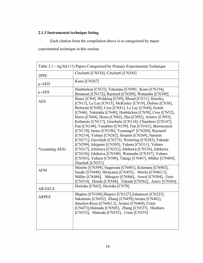
2.1.3 Instrumental technique listing
Each citation from the compilation above is re-categorized by major
experimental technique in this section.
Table 2.1 - Ag/Si(111) Papers Categorized by Primary Experimental Technique
2PPE Cinchetti [CN518], Cinchetti [CN545]
µ-AED Kono [CN267]
µ-AES Hanbücken [CN72], Tokutaka [CN99] , Kono [CN154], Boutaoui [CN172], Raynerd [CN209], Watanabe [CN349]
AES
*(scanning AES)
Bauer [CN4], Wehking [CN9], Rhead [CN11], Housley [CN13], Le Lay [CN15], McKinley [CN19], Dufour [CN38], Bolmont [CN40], Cros [CN41], Le Lay [CN44], Gotoh [CN46], Tokutaka [CN48], Hanbücken [CN50], Cros [CN52], Horio [CN64], Horio [CN82], Zhu [CN92], Aristov [CN93], Kohmoto [CN117], Grazhulis [CN118], Chambers [CN147], Fan [CN148], Venables [CN159], Fan [CN161], Borensztein [CN170], Inoue [CN196], Yasunaga* [CN204], Raynerd [CN214], Yuhara [CN262], Saranin [CN269], Saranin [CN271], Gavriljuk [CN273], Weitering [CN283], Fukuda [CN299], Ishigami [CN303], Yuhara [CN311], Yuhara [CN317], Ichimiya [CN321], Ishikawa [CN334], Ishikawa [CN338], Ishikawa [CN340], Watanabe [CN357], Yuhara [CN363], Yuhara [CN380], Takagi [CN467], Müller [CN484], Zhachuk [CN531]
AFM Minobe [CN399], Sugawara [CN401], Kitamura [CN402], Sasaki [CN448], Hirayama [CN455], Morita [CN462.5], Müller [CN484], Márquez [CN486], Aswal [CN504], Goto [CN514], Honda [CN548], Tokuda [CN562], Aseev [CN564]
AR-EELS Horioka [CN62], Horioka [CN70]
ARPES Shapiro [CN100],Shapiro [CN127],Johansson [CN223], Sakamoto [CN452] Zhang [CN459],Arranz [CN462], Sánchez-Royo [CN462.2], Arranz [CN464], Crain [CN473],Matsuda [CN505], Zhang [CN527], Hirahara [CN532], Matsuda [CN552], Crain [CN555]

19
Table 2.1 (Continued)
ARUPS
*(ARUPS Review)
McKinley [CN19], Hansson [CN33], Hansson [CN35], Hanbücken [CN50], Cros [CN52], Houzay [CN59], Yokotsuka [CN61], Wachs [CN73], Wachs [CN91], Ardehali [CN134], Johansson [CN156], Kono [CN162], Jiang [CN352], Pervan [CN353], Okuda* [CN359], Hasegawa [CN360], Nakajima [CN367], Tong [CN369], Viernow [CN372], Tong [CN428], Tong [CN456], Zhang [CN457], Matsuda [CN458], Matsuda [CN466], Gurnett [CN477]
b-SEI Doust[CN153], Venables [CN159]
Capacitance Muret [CN53]
Chemi-current Nienhaus [CN413]
Cyclic Voltametry Márquez [CN486], Ye [CN560]
DRS
Photoreflectance
303 Borensztein [CN170], 532 Borensztein [CN296]
EELS
*(HREELS)
Derrien [CN17], Gaspard [CN25], Cros [CN41] Layet* [CN84], Inaoka [CN550], Yu* [CN563]
Electrical
Conductivity
Schad [CN218], Hasegawa [CN225], Hasegawa [CN243], Heun [CN256], Luo [CN287], Kimberlin [CN307], Kampen [CN314], Cvikl [CN326], Cvikl [CN327], Ino [CN330], Jiang [CN344], Tong [CN356], Hasegawa [CN370], Henzler [CN400], Hasegawa [CN507], Keffous [CN520], Matsuda [CN530], Diagne [CN549]
Electromigration Yasunaga [CN131], Yasunaga [CN231]
ERDA Oura[CN168], Naitoh [CN181], Oura [CN417]
EXAFS
*(SEXAFS)
^(NEXAFS)
Sancrotti [CN247] Stöhr* [CN57], Stöhr* [CN68], Phillips^ [CN561]
FIM Park [CN132]
GIXRD
*(GIXRD-CTR)
Hong [CN217], Akimoto [CN379], Sarkar [CN429], Tajiri [CN451], Hata* [CN480], Takahashi [CN496], Tajiri [CN593], Tajiri [CN490]
GIXRF Yamanaka [CN513]

20
Table 2.1 (Continued) HEED Shapiro [CN127] ICB Cvikl [CN453] ICISS *(CAICISS) ^(TOF-ICISS)
Aono [CN86], Porter [CN124], Oura [CN128], Chang [CN138], Sumitomo [CN144], Williams [CN145], Daley [CN173], Kamiya* [CN184], Katayama* [CN185], Sumitomo^ [CN194], Aono* [CN228]
IID Inoue [CN196], Ishikawa [CN381] µ-SAM Tokutaka [CN99] Ion Channeling Watamori [CN115], Oura [CN128], Jin [CN151], Watamori
[CN163], Smith [CN165], Sundaravel [CN392] IPE Glass [CN469]
ISS *(Ion Profiling)
Narusawa [CN37], Cros* [CN41], Saitoh [CN43], Watamori [CN115], Shoji [CN116], Shoji [CN133]
ITCS Ino [CN242] ITDS Kern [CN12], Le Lay [CN15], Ino [CN242], Sato [CN260],
Müller [CN285], Ishigami [CN303] KRIPES Nicholls [CN95], Nicholls [CN96], Kono [CN162] laser-photovoltage Cahill [CN193] LEED ^(LEED-IV) *(LEED-CMTA) †(SPA-LEED)
Spiegel [CN1], Bauer [CN2], Bauer [CN4], Le Lay [CN7], Le Lay [CN8], Wehking [CN16], McKinley [CN19], Bolmont [CN32], Oura [CN34], Terada* [CN42], Saitoh [CN43], Le Lay [CN44], Terada* [CN49], Le Lay [CN60], Horioka^ [CN62], Yang^ [CN87], Aristov [CN93], Grazhulis [CN118], Shoji [CN133], Fan^ [CN148], Fan^ [CN161], Oura [CN168], Naitoh [CN181], Zuo [CN201], Henzler† [CN227], Jia [CN241], Jia* [CN241], Wan [CN244], Fan^ [CN253], Roos [CN257], Yuhara [CN262], Jia* [CN265], Saranin [CN269], Gavriljuk [CN273], Over^ [CN275], Nogami [CN279], Weitering [CN283], Luo^ [CN287], McComb [CN290], Zuo [CN297], Yuhara [CN311], Yuhara [CN317], Over^ [CN319], Zhang [CN322], Ishikawa [CN340], Schmitsdorf [CN343], Zuo† [CN362], Yuhara [CN363], Park [CN375], Yuhara [CN380], Henzler† [CN409], Moresco† [CN431], Yuhara [CN440], Sakamoto [CN452], Tong [CN456], Zhang [CN457], Matsuda [CN458], Zhang [CN459], Matsuda [CN466], Takagi [CN467], Tang [CN476], Gurnett [CN477], Kuntze [CN478], Pérez-Dieste [CN501], Ryjkov [CN522], Zhang [CN527], Zhachuk [CN531], Matsuda [CN552]
LEEM Denier van der Gon [CN236], Denier van der Gon [CN239], Tersoff [CN250], Tang [CN476]
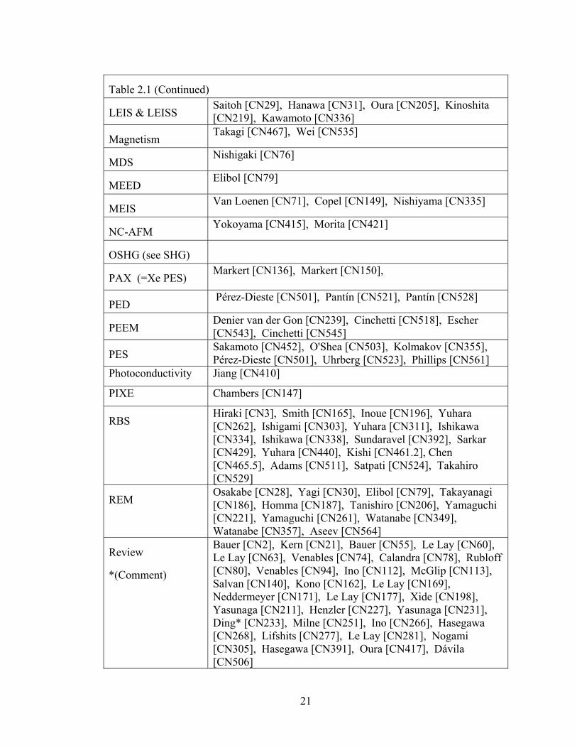
21
Table 2.1 (Continued)
LEIS & LEISS Saitoh [CN29], Hanawa [CN31], Oura [CN205], Kinoshita [CN219], Kawamoto [CN336]
Magnetism Takagi [CN467], Wei [CN535]
MDS Nishigaki [CN76]
MEED Elibol [CN79]
MEIS Van Loenen [CN71], Copel [CN149], Nishiyama [CN335]
NC-AFM Yokoyama [CN415], Morita [CN421]
OSHG (see SHG)
PAX (=Xe PES) Markert [CN136], Markert [CN150],
PED Pérez-Dieste [CN501], Pantín [CN521], Pantín [CN528]
PEEM Denier van der Gon [CN239], Cinchetti [CN518], Escher [CN543], Cinchetti [CN545]
PES Sakamoto [CN452], O'Shea [CN503], Kolmakov [CN355], Pérez-Dieste [CN501], Uhrberg [CN523], Phillips [CN561]
Photoconductivity Jiang [CN410]
PIXE Chambers [CN147]
RBS Hiraki [CN3], Smith [CN165], Inoue [CN196], Yuhara [CN262], Ishigami [CN303], Yuhara [CN311], Ishikawa [CN334], Ishikawa [CN338], Sundaravel [CN392], Sarkar [CN429], Yuhara [CN440], Kishi [CN461.2], Chen [CN465.5], Adams [CN511], Satpati [CN524], Takahiro [CN529]
REM Osakabe [CN28], Yagi [CN30], Elibol [CN79], Takayanagi [CN186], Homma [CN187], Tanishiro [CN206], Yamaguchi [CN221], Yamaguchi [CN261], Watanabe [CN349], Watanabe [CN357], Aseev [CN564]
Review
*(Comment)
Bauer [CN2], Kern [CN21], Bauer [CN55], Le Lay [CN60], Le Lay [CN63], Venables [CN74], Calandra [CN78], Rubloff [CN80], Venables [CN94], Ino [CN112], McGlip [CN113], Salvan [CN140], Kono [CN162], Le Lay [CN169], Neddermeyer [CN171], Le Lay [CN177], Xide [CN198], Yasunaga [CN211], Henzler [CN227], Yasunaga [CN231], Ding* [CN233], Milne [CN251], Ino [CN266], Hasegawa [CN268], Lifshits [CN277], Le Lay [CN281], Nogami [CN305], Hasegawa [CN391], Oura [CN417], Dávila [CN506]

22
Table 2.1 (Continued)
RHEED
*(RHEED-TRAXS)
^(RHEED-SWR)
+(RHEED-00 Spot)
Le Lay [CN7], Le Lay [CN8], Ino [CN14], Gotoh [CN18], Ichikawa [CN26], Gotoh [CN54], Horio^ [CN64], Horio+ [CN67], Gotoh [CN69], Hanbücken [CN75], Futamoto [CN77], Hasegawa* [CN81], Horio [CN82], Hasegawa* [CN105], Ino* [CN112], Kohmoto [CN117], Park* [CN132], Jalochowski [CN135], Ichimiya [CN142], Kohmoto [CN155], Fan [CN166], Fukutani* [CN199], Hasegawa [CN225], Yamanaka* [CN237], Ino* [CN242], Hasegawa [CN243], Yamanaka* [CN249], Roos [CN255], Roos [CN257], Ino* [CN266], Roos [CN278], Naik [CN286], Hasegawa [CN289], Biswas [CN298], Ichimiya [CN300], Yamanaka* [CN316], Zhang [CN318], Ichimiya [CN321], Lijadi [CN339], Nakajima [CN350], Zhang [CN351], Jiang [CN352], Tong [CN356], Hasegawa [CN370], Tong [CN373], Miki [CN385], Blankenship [CN403], Tong [CN428], Matsuda [CN458], Yamanaka* [CN482], Kimberlin [CN510], Yamanaka [CN513], Goto [CN514], Nakahara [CN534], Wei [CN535], Honda [CN548]
RHEPD Fukaya [CN544]
SAM
*(SAM Review)
Yasunaga [CN131], Wu [CN180], Yasunaga* [CN182], Yasunaga [CN211], Wu [CN213], Yasunaga [CN222]
SBH I-V Van Otterloo [CN10], Van Otterloo [CN36], Weitering [CN245], Schmitsdorf [CN313], Weitering [CN329], Cvikl [CN383], Hirayama [CN470], Keffous [CN520]
SEE (Angle
Scanned)
Endo [CN332]
SEM
*(FE-SEM)
Venables[ CN22], Gotoh[ CN54], Hanbücken[ CN72], Hanbücken[ CN75], Futamoto[ CN77], Hanbücken[ CN85], Tokutaka[ CN99], Gotoh [CN114], Doust [CN153], Venables [CN159], Park [CN160], Boutaoui [CN172], Nason [CN189], Huang [CN210], Raynerd [CN214], Nason [CN226], Naitoh* [CN235], Ino [CN242], Milne [CN251], Endo [CN270], Endo [CN274], Ohnishi [CN312], Zhang [CN322], Ino [CN330], Metcalfe [CN346], Watanabe [CN349], Watanabe [CN357], Hasegawa [CN370], Shi [CN432], Sarkar [CN435], Glass [CN469], Yamanaka [CN482], Müller [CN484], Márquez [CN486], Hirayama* [CN499], Hasegawa [CN507], Adams [CN511]
SEXAFS (See EXAFS)
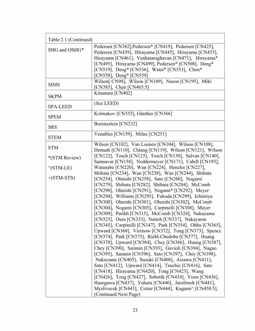
23
Table 2.1 (Continued)
SHG and OSHG* Pedersen [CN382],Pedersen* [CN419], Pedersen [CN425], Pedersen [CN439], Hirayama [CN445], Hirayama [CN455], Hirayama [CN461], Venkataraghavan [CN471], Hirayama* [CN495], Hirayama [CN499], Pedersen* [CN508], Deng* [CN519], Deng* [CN536], Watai* [CN553], Chen* [CN558], Deng* [CN559]
SIMS Wilson[ CN98], Wilson [CN109], Nason [CN195], Miki [CN385], Chen [CN465.5]
SKPM Kitamura [CN402]
SPA-LEED (See LEED)
SPEM Kolmakov [CN355], Günther [CN366]
SRS Borensztein [CN232]
STEM Venables [CN159], Milne [CN251]
STM
*(STM Review)
^(STM-LE)
+(STM-STS)
Wilson [CN102], Van Loenen [CN104], Wilson [CN108], Demuth [CN110], Chiang [CN119], Wilson [CN121], Wilson [CN122], Tosch [CN125], Tosch [CN130], Salvan [CN140], Samsavar [CN158], Neddermeyer [CN171], Cahill [CN193], Watanabe [CN220], Wan [CN224], Henzler [CN227], Shibata [CN234], Wan [CN238], Wan [CN244], Shibata [CN254], Ohnishi [CN258], Sato [CN260], Nogami [CN279], Shibata [CN282], Shibata [CN284], McComb [CN290], Ohnishi [CN291], Nogami* [CN292], Meyer [CN294], Williams [CN295], Fukuda [CN299], Ichimiya [CN300], Ohnishi [CN301], Ohnishi [CN302], McComb [CN304], Nogami [CN305], Carpinelli [CN308], Meyer [CN309], Parikh [CN315], McComb [CN324], Nakayama [CN325], Oura [CN333], Naitoh [CN337], Nakayama [CN345], Carpinelli [CN347], Park [CN354], Ohba [CN365], Upward [CN368], Viernow [CN372], Tong [CN373], Spence [CN374], Park [CN375], Riehl-Chudoba [CN377], Huang [CN378], Upward [CN384], Chey [CN386], Huang [CN387], Chey [CN390], Saranin [CN393], Gavioli [CN394], Nagao [CN395], Saranin [CN396], Sato [CN397], Chey [CN398], Nakayama [CN405], Suzuki [CN408], Aizawa [CN411], Sato [CN412], Upward [CN414], Tsuchie [CN416], Sato [CN418], Hirayama [CN420], Tong [CN423], Wang [CN426], Tong [CN427], Sobotík [CN434], Yoon [CN436], Hasegawa [CN437], Yuhara [CN440], Jarolímek [CN441], Myslivecek [CN443], Cotier [CN444], Kagami^ [CN450.5], (Continued Next Page)
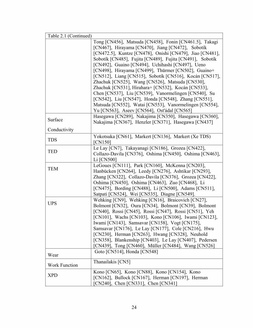
24
Table 2.1 (Continued)
Tong [CN456], Matsuda [CN458], Fonin [CN461.5], Takagi [CN467], Hirayama [CN470], Jiang [CN472], Sobotík [CN472.5], Kuntze [CN478], Onishi [CN479], Jiao [CN481], Sobotík [CN485], Fujita [CN489], Fujita [CN491], Sobotík [CN492], Guaino [CN494], Uchihashi [CN497], Ueno [CN498], Hirayama [CN499], Thürmer [CN502], Guaino+ [CN512], Liang [CN515], Sobotík [CN516], Kocán [CN517], Zhachuk [CN525], Wang [CN526], Matsuda [CN530], Zhachuk [CN531], Hirahara+ [CN532], Kocán [CN533], Chen [CN537], Liu [CN539], Vanormelingen [CN540], Su [CN542], Liu [CN547], Honda [CN548], Zhang [CN551], Matsuda [CN552], Watai [CN553], Vanormelingen [CN554], Yu [CN563], Aseev [CN564], Ost'ádal [CN565]
Surface
Conductivity
Hasegawa [CN289], Nakajima [CN350], Hasegawa [CN360], Nakajima [CN367], Henzler [CN371], Hasegawa [CN437]
TDS Yokotsuka [CN61], Markert [CN136], Markert (Xe TDS) [CN150]
TED Le Lay [CN7], Takayanagi [CN186], Grozea [CN422], Collazo-Davila [CN376], Oshima [CN450], Oshima [CN463], Li [CN500]
TEM LeGoues [CN111], Park [CN160], McKenna [CN203], Hanbücken [CN264], Leedy [CN276], Ashtikar [CN293], Zhang [CN322], Collazo-Davila [CN376], Grozea [CN422], Oshima [CN450], Oshima [CN463], Zuo [CN468], Li [CN475], Bording [CN488], Li [CN500], Adams [CN511], Satpati [CN524], Wei [CN535], Diagne [CN549].
UPS Wehking [CN9], Wehking [CN16], Braicovich [CN27], Bolmont [CN32], Oura [CN34], Bolmont [CN39], Bolmont [CN40], Rossi [CN45], Rossi [CN47], Rossi [CN51], Yeh [CN101], Wachs [CN103], Kono [CN106], Iwami [CN123], Iwami [CN143], Samsavar [CN158], Vogt [CN175], Samsavar [CN176], Le Lay [CN177], Cole [CN216], Hwu [CN230], Herman [CN263], Hwang [CN328], Neuhold [CN358], Blankenship [CN403], Le Lay [CN407], Pedersen [CN439], Tong [CN460], Müller [CN484], Wang [CN526]
Wear Goto [CN514], Honda [CN548]
Work Function Thanailakis [CN5]
XPD Kono [CN65], Kono [CN88], Kono [CN154], Kono [CN162], Bullock [CN167], Herman [CN197], Herman [CN240], Chen [CN331], Chen [CN341]

25
Table 2.1 (Continued)
XPS
*(Soft XPS)
^(ESCA imaging)
Dufour [CN38], Kono [CN88], Yeh* [CN89], Schleberger [CN320], Schmitsdorf [CN343], Jiang [CN352], Tong [CN369], Grozea [CN422], Sarkar [CN429], Glass [CN469], Kovac [CN483], Aswal [CN504], Goto [CN514], Escher^ [CN543]
X-Ray Topography Takahashi [CN178]
XRD
*(XRD-CTR)
^(XRD-Laue)
Takahashi [CN126], Vlieg [CN137], Takahashi [CN139], Vlieg [CN141], Park [CN160], Takahashi^ [CN178], Takahashi [CN229], Takahashi [CN252], Leedy [CN276], Naik [CN286], Aburano* [CN310], Aburano* [CN323], Hata* [CN424], Horii [CN447], Takahiro [CN529], Tokuda [CN562]
XSW Vlieg [CN191], Vlieg [CN200], Woicik [CN348]
2.1.4 Theoretical/computational technique listing
Table 2.2 - Ag/Si(111) Papers Categorized by Primary Theoretical Technique
Experimental Technique Modeling AFM 1st Principles Sasaki [CN465], Sasaki [CN430] ARXPS Fujikawa [CN174] Conductivity Percolation Theory Luo [CN287] EELS LCAO Gaspard [CN25] ICB Korosak [CN442] ICISS Chaudhury [CN246] LEED QK-LEED Jia [CN265]
General Watanabe [CN208], Watanabe [CN215], Watanabe [CN248], Nakamura [CN454]
LCAO Watanabe [CN220],Watanabe [CN248]
STM
LDF Watanabe [CN208], Nagayoshi [CN207]
Linear response theory Nazarov [CN474] OSHG Non-linear response Pedersen [CN425]
XPD Dynamical theory Chen [CN341]

26
Table 2.2 (Continued)
Theoretical and Calculational Methods Total E and E minimization
1st principles Chan [CN146], Ding [CN272], Nakamura [CN487], Liang [CN515], Chen [CN537], Jeong [CN541], He [CN546], Zhang [CN551]
E minimization Tech. Barone[ CN24], Northrup [CN97], Ratsch [CN259]
DF and LDF/LDA Techniques
Meade [CN152], Chan [CN164], Ding [CN202], Nagayoshi [CN207], Aizawa [CN406], Aizawa [CN411], Sasaki [CN433], Sasaki [CN448], Kakitani [CN449]
Cluster calculations Hoshino[ CN58], Jingguang[ CN83], Zheng [CN120], Chou [CN129], Fortunelli [CN183], Kirchner [CN280], Chen [CN331]
Band Structure Calculations Nagayoshi[ CN90], Kirchner [CN306], Erwin [CN388]
Step-Surface Energetics Freudenhammer[ CN23], Balamane [CN157], Tong [CN190], Jin [CN438]
Surface Energetics, Nucleation and Growth Energetics Kinetics
Bermond[CN66], Venables [ CN74], Venables [CN94], Venables [CN107]
Monte Carlo Techniques *(Kinetic MC Techniques)
Natori [CN179], Kempa [CN364], Myslivecek* [CN443], Nakamura [CN446], Kakitani [CN449], Sobotík [CN485], Nakamura [CN487], Ostádal [CN493], Kocán [CN517], Kocán [CN533]
Diffusion Theory Raynerd [CN214], Venables [CN288] LCAO Methods Jingguang[ CN83], Watanabe [CN220],
Watanabe [CN248] MD Simulations Biswas [CN298], Bording [CN488],
Pizzagalli [CN509] Self-consistent Hartree-Fock Julg[ CN56] Lattice Gas Calculations Natori [CN342] Thermodynamics Rhead[ CN11] Tight Binding Kobayashi [CN557] Twist Boundary Xin [CN556] Work Function Andrews [CN6]

27
2.2 Ag/Si(111) surface phase diagram reconstruction
2.2.1 Overview
By scouring the literature for references to specific Ag/Si(111) phase
observations and correlating that with the corresponding surface preparation
technique, a new 2D surface phase diagram for the system has been constructed as
shown in the slightly idealized form of Figure 2.3.
Figure 2.3 - Idealized surface structure diagram for Ag/Si(111).
In this phase diagram format with surface structural regions plotted on standard
temperature vs. coverage axes, the reader should note the following. To the right of
the figure are defined temperature “regimes” of cryogenic, low, ambient, elevated,
high, desorption and flash that will aid future discussions. In the lower left of the

28
figure, low Ag coverage at temperatures below 200°C, Ag on Si(111)-(7x7) deposits
in a disorganized fashion. As temperature increases to near 200°C and Ag coverage
approaches 1 ML, there is a complex and mixed attempt to organize into Ag-(1x1) or
Ag(111) crystallites. Moving into the lower right portion of the diagram, as coverage
increases in these cryogenic, low and ambient temperatures, Ag grows in layer-by-
layer, Frank-van der Merwe fashion only at cryogenic temperatures. Increasing
temperature at high coverages initiates what has been termed, “pseudo F-M” growth.
In this mode, Ag atoms reaching the low and ambient temperature surface have
sufficient energy to migrate and the overlayer grows by an island growth and
coalescence mode with temperature determining the island size, distribution and
growth rates. These pseudo-F-M Ag(111) islands grow with two, twin-related
orientations until about 100°C where the Ag <110> || Si <110> orientation dominates.
As we move to the upper two thirds of Figure 2.3, temperatures above 200°C
and low Ag coverage, there is the appearance of the Ag-(√3x√3)R30° phase in β- and
γ- forms. As temperatures further increase into the desorption regime, Ag atoms
emanate from the surface leaving the Ag-(3x1) phase before transitioning to the clean
Si(111)-(7x7) then Si(111)-(1x1) phases. For high coverages, the √3-Ag phase forms
first and additional Ag grows in classic layer-plus-island, Stranski-Krastanov (S-K)
mode until a temperature of about 450°C. Above this temperature, the sticking
coefficient for new Ag atoms onto the √3-Ag surface is zero and any existing Ag(111)
islands desorb at known temperature-dependant rates.
2.2.2 Low coverage, low temperature region
To support the features of this new surface phase diagram, it is necessary to
look at each quadrant of Figure 2.3 in detail. Starting with the low coverage, low
temperature portion, an expanded and annotated view is presented as Figure 2.4. At

29
the lowest coverage and temperature, the series of open circles indicate the onset of
surface conductivity. These measurements in and of themselves, do not aid with phase
identification. However, percolation theory predicts that the perfect random placement
of conductors on a surface will create a conduction path at a coverage of 0.5 ML.
Thus doubling the coverage determined by conduction experiments can place the
monolayer coverage boundary at these low temperatures. This procedure produces a 1
ML boundary line is excellent agreement with four other conductivity and RHEED
measurements of complete coverage at cryogenic temperatures, solid circles in the
figure. How is the shallow slope of the boundary explained? This author proposes the
following. First, there is a point at -188°C where surface conductivity is complete at
0.5 ML where Ag/Si(111) behaves as an ideal percolation model material. At
temperatures below this ideal point, lateral movement of an incoming Ag atom
becomes increasingly restricted. Those atoms that find themselves deposited atop
previous Ag adsorbates remained trapped away from the surface and unable to
contribute to the conduction link. At temperatures above this ideal point, Ag
adsorbates easily ‘climb down’ from deposited positions atop Ag islands and can
migrate with increasing ease to larger and larger island groups.
Moving into the low and ambient temperature range from roughly -150°C to
+100°C, knowledge of the surface dynamics comes increasingly from STM and
RHEED observations. Even at -123°C, Ag atoms arriving at a surface with typical 2-3
eV thermal energies have a radius of non-thermal migrationCN278 greater than 50 Å.

30
Figure 2.4 - Low coverage, low temperature quadrant of the Ag/Si(111)-(7x7) surface structure diagram

31
As room temperature approaches, the long thermal diffusion lengths allow Ag
atom placement to evolve from random to a more organized but not yet crystalline
structure. At the lowest coverages, < 0.1 ML, Ag is not imaged but its effect on the
underlying Si(111)-(7x7) structure is noted. The Ag is thought to initially drop into
the Si(111)-(7x7) corner holes. ShibataCN282 calls this the "first stage α-island"
structure. Increasing Ag coverage produces a "second stage α-island" structure imaged
in STM as a bright-spot, empty-state located at the center of the (7x7) faulted half.
Further condensation produces a third stage α-island structure consisting of a ring-like
shape on the faulted (7x7) half. Further growth at R.T. consists of coalescence of
these α-island structures to form a smooth uniform structure. The critical coverage at
near-room temperatures is ill-determined as seen by the six solid circle determinations
indicated in the figure. Above 0.5 ML, the surface is in concurrent transition between
a continued random, organized, Ag-(1x1), Ag(111) or 3D Ag crystallite ending phase.
This is an unfortunate happenstance of this surface system since room-temperature
structures are, by definition, the simplest and most widely probed. This fundamental
characteristic of the system has contributed greatly to the overall complexity and
confusion about the physics of Ag/Si(111).
2.2.3 High coverage, low temperature region
An expanded and annotated view of the lower right quadrant of Figure 2.3 is
shown in Figure 2.5. (Note the 10X increase in the horizontal scale factor.) At the
lowest, cryogenic temperatures, it is agreed that Ag grows in F-M fashion denoted as
the α-Ag(111) growth region. The upper limit on this F-M growth mode ranges from
-183°C CN135 upwardCN458 to -117°CCN289 depending on technique with reports that the
transition is coverage but not temperature dependant starting at 6 MLCN351 and
contradictory reports that the transition is temperature but not coverage

32
dependantCN309, CN135. This author asserts that this is a continuum transition, with
inhibited micro-island nucleation, growth and coalescence as the growth mechanism,
and assigns the transition temperature of -188°C discussed in the previous section.
Even at these low temperatures, Ag(111) forms parallel to Si(111), loosing epitaxy
only after deposit thicknesses greater than 1000 Å.
Above this α-Ag(111) region, denoted the β-Ag(111) pseudo F-M region.
Ag(111) forms epitaxially with two, twin related orientations of Ag(111) Si(111)
and Ag<110> Si<110> as well as Ag<112> Si<110>. This region has S-K as well
as F-M like characteristics depending on technique used to probe it. At even higher
temperatures the γ-Ag(111) pseudo F-M growth region begins at roughly 130°C
(depending on deposition rate). This γ-Ag(111) continues to form epitaxially but only
in the ideal Ag(111) Si(111) and Ag<110> Si<110> orientation. As indicated with
the dash-dot line in Figure 2.5, this pseudo F-M phase can be moved to substantially
higher temperatures with sufficiently rapid Ag deposition rates. The low coverage
portion of this region, from 1 to 3 ML is labeled “proto” since the great majority of
papers defer phase definition until unambiguous LEED or RHEED patterns appear.
There is a critical and fundamental transition at approximately 200°C the upper
portion of Figure 2.5 traversing all coverages as seen previously in the overview of
Figure 2.3 and detail of Figure 2.4. Estimates for this transition range from 190°C at
the low endCN297 to 290°C at the highCN114. It is essential that the reader understand
that this transition is due to the tertiary interactions of Ag, Si(111)-(7x7) adatoms and
Si(111)-(7x7) dimer-stacking fault substrate. That is, the Si self-adatoms in the
presence of Ag acting as a surfactant, can restructure to allow an Ag to Si(substrate)
coupling. This line establishes the great divide between lower temperature, weakly-
interacting Ag/Si and the higher temperature, much stronger bonding Ag-√3 and Ag S-
K growth dichotomy.

33
Figure 2.5 - High coverage, low temperature quadrant of the Ag/Si(111)-(7x7) surface structure diagram

34
2.2.4 Low coverage, high temperature region
Figure 2.6 expands and annotates the upper left quadrant, the high temperature
low coverage portion, of Figure 2.3. This is the region wherein lies the greatest
controversy about the structure of the Ag-(√3x√3)R30° phase. As noted in the
paragraph above, the Ag-√3 phase is able to form at temperatures above ~200°C
where sufficient thermal energy exists, in connection with Ag adatoms, to reorder the
Si self-adatoms of the Si(111)-(7x7) DAS surface. It is the movement, incorporation
and segregation of these Si atoms by or into the √3 structure that this author considers
to be one of the outstanding unanswered questions in surface science today.
There is no dispute that Ag/Si(111) forms the √3 structure for all Ag coverages
at temperatures of 200°C and above (until desorption). Presented here instead, is the
first compilation of observations and anecdotal evidence supporting the concept of
multiple forms of the phase, christened β-√3 and γ-√3 for the 2/3 and 1 ML versions
respectively. Determination of a complete monolayer coverage in the β- and γ-regions
have been attempted in nineteen papers as shown by the open circles in Figure 2.6.
The most complete study delineated by the dash-dot-dash connecting line is by
RaynerdCN209 using µ-AES. Their data provides a convenient outer envelope for all
other determinations with the exception of one outlyer.CN088 The combined result is
conceptually similar to that proposed in 1981 by LeLayCN044 followed closely by
JulgCN056 in 1982, where the √3 layer is initially formed with 2 Ag atoms per surface
unit cell (2/3 ML coverage) until additional thermal energy of 0.1 eV is available to
allow a third Ag atom (1 ML coverage total) to traverse an activation barrier to
complete the phase.

35
Figure 2.6 - Low coverage, high temperature quadrant of the Ag/Si(111)-(7x7) surface structure diagram

36
In addition to the data points plotted above, there have been numerous other
citings of an anecdotal nature detailing the variability of Ag/Si(111) critical coverage.
Le LayCN044 noted that θc increases as Tsubstrate increases (θc varies from 0.8 to 1.0 at
500°C) and θc = 2/3 at 200°C. RaynerdCN236 demonstrated that θc is deposit path
dependant and can be 2/3 or 1. HasegawaCN105 and later InoCN242 showed critical
coverage temperature dependency with; θc = 0.8 ± 0.1 ML for Ag-√3 produced at 480
°C and θc = 0.9 ± 0.1 ML for Ag-√3 produced at 440 °C. IshigamiCN303 conjectured
that Ag forms two different √3 structures, one for Ag coverage >0.5ML and another
for coverage <0.5ML. In all, the concept that critical coverage can be a changing
function has been independently observed by a number of researchers but ignored by
the sub-field in general while searching for the one correct solution to the structure of
Ag-(√3x√3)R30° on Si(111).
The assertion by this author that there exists β- and γ- forms of the Ag-√3
structure comes not only from the experimental results presented later in Chapter 5
and the unusual 2/3 to 1 ML transition in the surface structure diagram of Figure 2.6
but also the following anecdotal evidence from the extensive literature database. The
earliest unaccounted indication of a multi-conformal √3 phase was noted in the ITDS
results of Hasegawa.CN105 Isothermally desorbing √3 phase created at 440°C shows a
break-point between the √3 and (3x1) phases. In contrast, √3 phase created at a higher
480°C temperature showed no such feature. Later, InoCN112 while isothermally
desorbing Ag√3 at temperatures between 560° and 585°C noted three independent
break points at 1, 2/3 and 1/3 ML respectively corresponding, this dissertation’s author
believes, to the γ-, β- and (3x1) phases. RaynerdCN214 pinned this unknown transition
temperature at 427°C, echoing Julg’s ideaCN056 [sic. LeLayCN044] of a 2/3 ML Ag-√3
phase extended by an additional 1/3 ML after an activation barrier is traversed.

37
At the upper portion of the diagram, in the desorption region above 550°C lies
the Ag-(3x1) metastable phase. Two important points must be emphasized. First, any
Ag phase on Si(111) held at temperatures above 550°C will desorb, so if the reader is
thinking of these structural diagrams as traditional phase diagrams, these Ag-(3x1) and
Ag-(√3x√3) are not there. There are no stable phases at these temperatures, Ag
completely desorbs leaving bare Si(111) with a residual 0.02ML equivalent of 2D
delocalized Ag adatom gas present at pressures below 3 x 10⁻⁸ torr. Desorption rates
for Ag/Si(111) phases are well documented even in the earliest literatureCN012 by
ITDS. Second, it is this author’s contention that coverage declarations in the literature
are suspect if measurements are made or samples prepared by transitioning into
desorption region or above unless careful notations of time at temperature are
included. The sloping upper boundary does not specify an exact transition but rather
connotes the general idea that phases are shorter lived as temperatures increase.
Understanding the metastable nature of all Ag phases at this temperature, the
reader can appreciate that a high coverage S-K growth of Ag(111) islands on Ag-√3
on Si(111) taken into the desorption regime will transition first from S-K to Ag-√3 by
desorption of Ag islands. Next the Ag-√3 phase will desorb at a slower rate, leaving
Ag-(3x1) phase. Finally, the Ag-(3x1) phase desorbs at a much slower rate yet,
leaving bare Si(111). Although the different phase desorption is considered to be
consecutive, STM images taken after high temperature exposure or in the proximity of
surface defects show simultaneous existence of Si(111)-(7x7), Ag-(3x1) and Ag-√3
phases.
Uppermost in the diagram is shown the broad Si(111)-(7x7) region that
remains after complete Ag desorption. Interestingly, a faint 0.02ML equivalent of 2D
Ag adatom gas remains as determined by electrical conductivity measurements.
Finally, above 830°C, Si(111)-(7x7) transforms into a Si(111)-(1x1) structure that
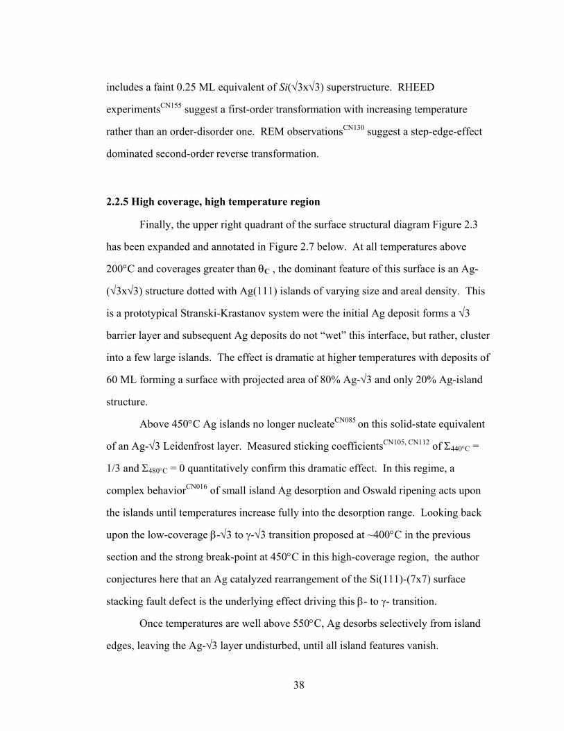
38
includes a faint 0.25 ML equivalent of Si(√3x√3) superstructure. RHEED
experimentsCN155 suggest a first-order transformation with increasing temperature
rather than an order-disorder one. REM observationsCN130 suggest a step-edge-effect
dominated second-order reverse transformation.
2.2.5 High coverage, high temperature region
Finally, the upper right quadrant of the surface structural diagram Figure 2.3
has been expanded and annotated in Figure 2.7 below. At all temperatures above
200°C and coverages greater than θC , the dominant feature of this surface is an Ag-
(√3x√3) structure dotted with Ag(111) islands of varying size and areal density. This
is a prototypical Stranski-Krastanov system were the initial Ag deposit forms a √3
barrier layer and subsequent Ag deposits do not “wet” this interface, but rather, cluster
into a few large islands. The effect is dramatic at higher temperatures with deposits of
60 ML forming a surface with projected area of 80% Ag-√3 and only 20% Ag-island
structure.
Above 450°C Ag islands no longer nucleateCN085 on this solid-state equivalent
of an Ag-√3 Leidenfrost layer. Measured sticking coefficientsCN105, CN112 of Σ440°C =
1/3 and Σ480°C = 0 quantitatively confirm this dramatic effect. In this regime, a
complex behaviorCN016 of small island Ag desorption and Oswald ripening acts upon
the islands until temperatures increase fully into the desorption range. Looking back
upon the low-coverage β-√3 to γ-√3 transition proposed at ~400°C in the previous
section and the strong break-point at 450°C in this high-coverage region, the author
conjectures here that an Ag catalyzed rearrangement of the Si(111)-(7x7) surface
stacking fault defect is the underlying effect driving this β- to γ- transition.
Once temperatures are well above 550°C, Ag desorbs selectively from island
edges, leaving the Ag-√3 layer undisturbed, until all island features vanish.

39
Researchers can balance and in some cases overwhelm this desorption path by surface
dosing at high rates but only transiently. At the highest temperatures the concept of
high Ag surface coverage becomes moot and the Si(7x7) and Si(111) behavior
described in the previous section applies.
2.2.6 Special case: deposition on Si(111)-(2x1)
A clean Si(111) surface created by cleaving rather than the more prevalent
chemical and thermal techniques, will form a characteristic Si(111)-(2x1) surface
structure. As seen in Figure 2.8, this clean (2x1) surface will convertCN023 into the
Si(111)-(7x7) structure at temperatures between 210° and 425°C depending upon
cleavage surface step density. If Ag is deposited on this Si(111)-(2x1) surface, two
unique phases, different than those previously discussed can form, both at ambient
temperatures.
Following the development used in the previous sections, examining Ag
deposition on Si(111)-(2x1) from low to high temperatures and low to high coverages,
the following changes occur. At the lowest temperatures, Ag randomly decorates the
Si(111)-(2x1) surface until Ag(111) F-M growth takes over at high coverages. This is
similar to the response on the Si(111)-(7x7) surface. There are a series of
experimentsCN118 that determine the temperature and coverage points where random
Ag/Si(111)-(2x1) transitions to Ag(1x1)/Si(111)-(2x1) and at higher coverages to
Ag(111) S-K growth. This behavior again parallels the Ag/Si(111)-(7x7) growth case.
Near room temperature however, phase behavior on Si(111)-(2x1) ceases to
model the behavior on Si(111)-(7x7). Ag coverage above 0.3 MLCN039 produces a
unique Ag(√7x√7)R19.1° structure on Si(111)-(2x1). It is notedCN118 that the
formation of this phase is sensitive to “vacuum conditions” in much the same way that

40
the formation of the high temperature, low coverage Ag(3x1)/Si(111)-(7x7) phase has
been found to be in this dissertation. As coverage increases, some Ag(111)-
(1x1)/Si(111)-(2x1) growth is already apparent and the Ag(√7x√7)R19.1° structure
continues to form. It is assertedCN044 that this Ag-√7 structure becomes complete at
6/7 ML. Continuing to increase coverage, Ag(111) island growth increases on
Si(111)-(2x1), the Ag-√7 LEED pattern still persists to 2 MLCN044 and a new
additional Ag(3x1)/Si(111)-(2x1) phase emerges at 1.5 MLCN008. Above 2.5 ML,
the Ag-√7 phase has faded leaving the Ag(111) and Ag(3x1) phases which catalyze a
Si(111)-(2x1) to Si(111)-(1x1) substrate changeCN123.
At higher than ambient temperatures there is a transition from these Si(111)-
(2x1) specific phases to the standard Ag-√3 and S-K growth on Si(111)-(7x7) phases.
The exact temperature and coverage transitions have not yet been explored in detail.
Certainly, at temperatures above 200°C for >1 ML coverages the transition has
occurred. At 400°C, it is knownCN021 that even 0.1 ML Ag coverage will readily
catalyze the Si(2x1) to Si(7x7) transition. Once this transition occurs, the surface
structural diagram for all practical purposes is equivalent to those previously presented
in Figure 2.6 and Figure 2.7.
There are many studies that prepare clean initial surfaces by cleaving at room
temperature then deposit Ag at elevated temperatures where the Si(111)-(2x1) surface
character is lost. The results of these studies have been included with the results
produced by Ag on Si(111)-(7x7) surfaces. It is recommended that the two
preparation methods be separated in future studies to determine if they have an effect
on coverage or surface structure findings.

41
Figure 2.7 - High coverage, high temperature quadrant of the Ag/Si(111)-(7x7) surface structure diagram

42
Figure 2.8 - Special case: surface structure diagram, Ag on cleaved Si(111)-(2x1)
43
2.2.7 Special case: over-deposition onto existing Ag-(√3x√3)R30°/Si(111)
A special processing case for Ag/Si(111)-(7x7), has yielded interesting results
including three additional new phases. Shown in Figure 2.9 are the cumulative results
for these special case surfaces produced by, first, creating a complete Ag-
(√3x√3)R30°/Si(111) surface at elevated temperatures then, second, over-depositing
Ag at cryogenic or low temperatures. It must be made perfectly clear that in this
Section 2.2.7, the starting surfaces already have an unknown quantity of Ag deposited
forming a base Ag-√3 structure. The Ag coverage plotted on Figure 2.9’s abscissa
represents the controlled amount in addition to the amount which was required to form
the Ag-√3 surface. It is the two step processing path, a high temperature step followed
by a low temperature step, that differentiates these surfaces from the other single
preparation results previously presented.
At the very lowest cryogenic temperatures and coverages Ag randomly
nucleates on the Ag-√3 surface. At low excess coverages and temperatures below -
175°C and after some short-range ordering of Ag upon initial deposit, a new Ag(6x6)
phase emergesCN356, stable only from roughly 0.2 to 0.5 ML before giving way to Ag
3D island growth with S-K characteristic.
Moving higher in temperature, -100 to -175°C, initial deposits show no, or at
best short range order, before organizing briefly into a Ag(√21x√21)R10.9°
configuration. Further deposits result in the brief appearance of the Ag(6x6) phase
before both are slowly replaced by Ag(111) 3D growth above 1ML excess coverage.
The Ag-√21 phase remains visible up through 2.5ML coverage and the Ag(6x6) phase
if formed remains until quenched at 1.75ML. Also in this temperature zone is an
important displacive transition in the underlying Ag-(√3x√3)R30° structure.CN490
Literature momentum suggest the elevated temperature Ag-√3 structure is best
described by one of the HCT or Honeycomb Chained Triangle models. Throughout

44
this dissertation, this author has labeled this the β-(√3x√3)R30° structure. At -123°C,
this underlying β-√3 makes a displacive transition to an α-(√3x√3)R30° structure
currently thought to match IET or Inequivalent Triangle model parameters. Both
models are explained generally in Section 2.4.3.
As temperature generally increases further, -100 to 0°C, the Ag-√21 and β-√3
structures dominate until S-K growth takes over. Above -75°C there is only a very
narrow low-coverage region of Ag-√21 stability, the remainder of growth looks
exactly like prototypical Ag(111) S-K growth covered in all previous Ag/Si(111)-
(7x7) diagrams. Also at these temperatures, the very lowest Ag deposits, <0.03ML
are known to be delocalized, forming a highly conductive 2D Ag atom gas. Higher
deposit amounts cause this delocalized layer to condense as the nuclei for 3D Ag
island growth.

45
Figure 2.9 - Special case: surface structure diagram, Ag on a pre-formed Ag-(√3x√3)/Si(111) surface.

46
2.3 Critical surface coverage determination for Ag-(√3x√3)R30° /Si(111)
One of the key points of contention in the search for a Ag-(√3x√3) model has
been the determination of the saturation, critical or completion coverage, denoted
equivalently as θS or θC. With the new evidence presented in the previous section, this
author has hoped to convince the reader that the Ag-√3 phase can accommodate both
two or three atoms per unit cell depending on preparation temperature, corresponding
to 2/3 and 1 monolayer θC respectively. The overwhelming majority of the research
however, has focused on finding the one correct model and thus the corresponding one
correct critical coverage. Historically shown in Figure 2.10, there raged a fierce
rivalry between 2/3 and 1 ML solutions during the years from 1975 to 1995.
Figure 2.10 - Historical trend; Ag-(√3x√3) phase critical surface coverage, θC.
With the emergence of a dominant model, the Honeycomb Chained Triangle or
HCT model, those papers expressly supporting a particular θC tended toward the 1
ML solution based upon the HCT model’s structural requirements rather than explicit
measurement. Overwhelmingly, the data points of Figure 2.10 which lie exactly on

47
the 2/3 or 1 ML range-values are specifically due to the support for one particular
model over another. Those data points lying between 1/3, 2/3 and 1 ML coverages,
especially those including error bars, are a result of experimental measurements of θC
rather than model dependant arguments.
To compliment the historical data analysis above, analyses of θC versus
Si(111) substrate properties; specifically substrate type, substrate dopant, substrate
resistivity and clean surface preparation temperature, were made but yielded limited
correlations. Results are shown in Figure 2.11. It was initially conjectured that boron,
a known delta-dopant and subsurface √3 forming element, could pattern the surface
for subsequent Ag-(√3x√3) phase formation. The top two Figure 2.11 graphs were a
check of that conjecture. Most authors report their substrates as p-type (including B)
or n-type. The 1:1 split between a θC of 1 and 2/3 ML for p-type as compared with a
2:1 ratio for n-type seemed to support that stance. Looking, however, at the smaller
subset of authors who actually reported the dopant element; B, P, As, Sb, etc. shows a
1:1 ratio for both p-type boron and n-type phosphorous substrates. Although the
sample set is small, only five total data points in the literature, this information plus
the experimental evidence to be presented in Chapter 5 indicates that trace B on
Si(111) does not influence Ag/Si(111) structure. Perhaps the discrepancy can be
explained by the influence of the quantity of dopant in addition to the type. This is
tracked in the figure’s lower left graph of critical coverage versus substrate resistivity,
where low resistivity means high dopant density and high resistivity indicates low
dopant density. It is shown that low resistivities (high dopant level) below 1 Ω-cm
show 1:2/3 ML ratio of ~2:1 where high resistivities revert to the 1:1 level tentatively
suggesting that high dopant levels influence structure. Of equal interest was the
provisional-correlation with clean Si(111) substrate preparation temperature shown in
the final, lower right graph of Figure 2.11. This author’s experience with high

48
temperature flashing of Si(111) wafer samples, presented later in Chapter 5, showed
optical indications of surface faceting and RBS indications of subsequent subsurface
Ag migration. It is still considered by this author, that surface flashing to temperatures
greater than 1000°C reformulates surface C into SiC and other surface phase
influencing impurities, defects and structures. Taking all data points at 1000°C and
below there appears to be a 1:1 split between θC of 1 and 2/3 ML. Summing points
above 1000°C gives the more normal 2:1 ratio seen in all other non-correlations. It is
tempting to count the discrepancy in favor of the stated bias toward low-temperature
surface cleaning cycles. Obviously, the two parameter correlation space used in the
figures are too simplistic and tenuous arguments given suggests further analysis is
appropriate.
Similar checks were made of Ag overlayer preparation methods. Re-analyzing
the literature data in terms of critical coverage against highest Ag covered surface
processing temperature lead to the construction of the surface structural diagram of
Figure 2.3 after all measured values θC were plotted and model determined values
were eliminated. Two other fascinating correlations emerged. The first, shown in
Figure 2.12, correlates critical coverage with the method for surface dosing with Ag.
As introduced in the thesis statement of Section 1.3, the effect carbon contamination
on subsequent Ag/Si structures was one of the three primary foci of this dissertation.
Not only are trace C contamination Auger peaks masked by Ag Auger satellites, but C
can easily co-deposited with Ag after clean surface preparation. One of the stealth
sources of contamination comes from carbon emitted from W filaments. Figure 2.12
shows the usual support of θC ratios 1ML:2/3ML of 2:1 for the unspecified Ag
deposition sources at far left and general source categories at far right. For those
authors who specify W filaments, wires, boats, coils, etc. the ratio becomes ~3:1.

49
Figure 2.11 - Null correlations; critical coverage vs. substrate type & dopant. Provisional correlations; resistivity& surface temp.

50
Figure 2.12 - Provisional correlation; critical coverage vs. Ag deposition source.

51
Figure 2.13 - Correlation; critical coverage vs. experimental method
52
Those specifying Ta or Mo filaments and crucibles, the ratio becomes 1:1 although the
sample size makes quantitation meaningless. The correlation for C contamination
from hot W deposition sources has been determined to be provisional. The second
quite surprising correlation is illustrated in Figure 2.13. This complicated plot
correlates critical coverage on the vertical axis against surface science experimental
method on the horizontal axis. The experimental methods are arranged first, by
primary incoming probe; electron, photon, ion then sub-categorized by outgoing
detection channel; electron, photon or ion as delineated on the top horizontal axis.
The electron probe techniques (AES, EELS, LEED, RHEED, SEM, etc.) have a
1ML:2/3ML support ratio of ~2:1 as in all other uncorrelated comparisons. Ion probe
techniques drop to a 1:1 support ratio and photon techniques almost exclusively
support the 1ML option. How can such a bias come about? Why would the non-
particle, photon in/ photon out, techniques exclusively favor the 1ML surface models?
The physical basis behind such a correlation eludes this author but is fascinating none
the less.
2.4 Surface model determination for Ag-(√3x√3)R30° /Si(111)
For the Ag-√3 phase alone, there have been eighteen distinct models proposed
with numerous variants within each model class. To simplify presentation and
analysis, these models will be categorized as; i) Ag independent, ii) Ag embedded or
iii) Ag on-top. In the first category, two models have been developed that either have
Ag atoms present strictly as a catalyst without primary organization or do not require
Ag atoms at all. Both produce the √3 structure via a organized Si reconstruction and
both are minor mentions in the structural development of Ag/Si(111), included for
completeness. In the second category, Ag embedded, the center of the Ag adsorbate is

53
at or below the center plane of the topmost Si atoms. Typically, large Si substrate
atom movement and strains are required. In the final category, Ag on-top, adatoms
decorate an in-tact or rearranged Si substrate in the more classic balls-on-a-Chinese-
checkerboard fashion.
From the literature database there have been 175 declarations of a favored
model. Of those, 2% favor the Ag independent, 35% favor the Ag embedded and 63%
prefer the Ag on-top models. What follows is a brief synopsis of each model. The
complex development, mutation and support for each model will be presented with
historical and contextual references in a future, more voluminous publication.
One of the problems with the model systems discussed below is the fact that
there is no ‘standard’ nomenclature system used to describe surface models. Model
naming has historically been left to the imagination of the model’s creator and,
especially in the Ag/Si(111) system, tremendous confusion has been purveyed when
one of two things happen. First, if the model anagram (ex. HCT = Honeycomb
Chained Trimer and Honeycomb Chained Triangle models) is not distinct confusion is
common. Second and more commonly, when an author makes a slight structural
change to an existing model and gives it a completely new moniker the historical link
is often lost. In addition, a model developed for one system is often applied to another
system and renamed by the author(s) for application in the new system and again, the
historical link is unobvious.
2.4.1 Ag independent models,
• D-Ag/Si V Model (Disordered Ag adsorbate / Stabilized Silicon
Vacancy): In this model the concept of ΘC is inapplicable but disordered
Ag is required. It was first proposed by YangCN087 in 1986, suggesting that

54
the √3 structure was due to a Silicon reconstruction with disordered
adsorbates of Ag or Ta catalyzing the transformation.
• SSV Model (Stabilized Silicon Vacancy): No adsorbate is needed at all,
therefore Θc = 0ML. Introduced by FanCN148 after observing that fast
1000°C flash cleaning and cooling can create a (√3x√3)R30° structure on
Si(111) without the presence of adatoms. LEED I-V measurements of this
√3 silicon vacancy structure are nearly identical to I-V measurements of a
0.6ML Ag-(√3x√3)/Si(111)-(7x7) surface.
2.4.2 Ag embedded models
• E (Embedded – general): There are many studies that have made
measurements of a general nature supporting an embedded vs. an atop
model so this category has been added to the following analyses.
• EH Model (Embedded Honeycomb): SaitohCN029, CN031 first proposed
embedding Ag below the Si(111) surface, between the two layers that
make up the surface double-layer with ΘC = 2/3 ML.
• ET Model (Embedded Trimer): With ΘC = 1ML, this embedded model
was first proposed by van LoenenCN104. Features include embedded Ag
trimers between the surface double-layers with 1/3 of the top surface Si
atoms per √3 unit cell removed forming an open Si honeycomb structure
on top of the embedded Ag structure. It’s construction is similar to the
Missing Top Layer model series later proposed so, for purposes of

55
analysis, the ET model is considered the first iteration in the MTL model
series and thus denoted equivalently, MTL-1.
• MTL Model (Missing Top Layer): This model with ΘC = 2/3 ordered
Ag + 1/3ML dilute Ag was proffered by KonoCN088 who refined calculated
positions for the Ag atoms as (0.15 ± 0.10)Å below the outermost Si layer
with a compression of the topmost Si 3-fold (H3) triangle from 3.84Å to
(2.7 ± 0.2)Å. This model is the first to propose that Ag sits above the
Si(111) double-layer but maintains an embedded Ag honeycomb
orientation by sitting above 3-fold, H3, double-layer sites of the bulk but
below a trimer Si structure made, presumably, of Si adatoms. This is
equivalent to AEH Model (Adatom Embedded Honeycomb) model
nomenclature sometimes used in the literature.
• SHCT Model (Silver Honeycomb Chained Trimer): ΘC = 1ML. Within
four months of Takahashi's HCT-1 modelCN126 journal submission detailed
below, VliegCN137 was the first to propose the SHCT model with similar
plan-view features but with Si adatoms sitting in the H3 sites created by
Ag trimers.
• ST Model (Substitutional Trimer): ΘC = 1ML by HorioCN082 who was
first to propose substituting Ag trimers for 1/3 missing top layer of the
surface double-layer Si atoms thus forming the √3 structure.
56
2.4.3 Ag on top models
• AST Model (Atop Sylil Trimer): ΘC = 1ML by WilliamsCN145 used the
Ag-triangle idea CN126 to create the AST model based on a chemically
intuitive Sylil Group (SiAg3) placed at atop sites on the Si(111) surface.
• AT Model (Atop Trimer): With ΘC =1 ML Wehking, et.al.CN016 was
the first to apply Lander and Morrison's* Trimer model proposed for
Al/Si(111) to the Ag/Si(111) system. They indicate that the Ag in the
trimers has near ionic diameter (2.52Å) when bonded to Si(111)CN126 for
this structure. The AT nomenclature was used before 1985 and is
equivalent to this author’s HCT-0 designation.
• CH Model (Centered Hexagon): With ΘC =1/3 ML, SpiegelCN001 placed
Ag residing at a hollow site in a centered hexagon configuration with Ag-
Ag nearest-neighbor distance of 6.6Å.
• HCT Model (Honeycomb Chained Trimer): Prior to 1985, this model
series was known as the AT or Atop Trimer Model. There was a period of
indiscriminate interchanging of the words “Trimer” and “Triangle” in the
HCT-type models much to everyone’s confusion. This AT or HCT model
is re-branded the HCT-0 model for this dissertation. As of the writing of
this dissertation, this model has emerged as the pre-eminent favorite for
the final structure of Ag/Si(111) so with historical hindsight, it was
possible to break out the sub-models into the HCT-x series listed below.
* J.J. Lander and J. Morrison, Surf. Sci. 2, 553 (1964) and J. Appl. Phys. 36, 1706 (1965).
57
• HCT-x Models (Honeycomb Chained Triangle): With ΘC = 1ML,
TakahashiCN126 was the first to propose this major variation of the
Honeycomb Chained Trimer model. This model also has characteristics in
common with the MTL series of models in that a final complete bulk-like
Si(111) double-layer is covered with a layer of Si atoms followed by a
layer of Ag atoms. It is also similar to the AT/HCT-0 model in the
appearance of Ag atoms in triangular formation bonded to a Si base-layer.
In the HCT-1 model, as we will designate this original Takahashi
proposalCN126, the ratio of the Ag triangle half-height to the √3 unit cell
side, x/a ratio, was calculated to be (0.44 ± 0.01) with the Ag atoms placed
zAg = (2.9 ± 0.1)Å above the in-tact surface double-layer. A Si-adatom
layer is proposed between the Ag and Si double-layer at a position 1Å
below the Ag layer.
• IET Model (Inequivalent Triangle): ΘC = 1ML. Building on the HCT-x
series of models, AizawaCN411 was the first to modify the Ag triangle
configuration and break the p31m surface symmetry by counter-rotating
the Ag triangles like in Over’sCN275 HCT-9R model, then also counter-
rotating the next layer Si triangles in the opposite direction and making
one of the two triangles in the surface unit cell larger than the other.
• q-HC Model (quasi-Honeycomb): ΘC = 1 ML. Kono, et.al.CN162 were
the first to propose a quasi-honeycomb model in which 1/3 of the Ag
atoms in the unit cell were displaced by 0.45Å into the surface and inter-
Ag atomic distances α1=4.4, α2=3.6 and β=3.1 Å .

58
• RCH Model (Rumpled Centered Hexagon): ΘC =2/3 and 1 ML.
LeLayCN012 proposed early in the model discovery history, that the Ag-√3
phase initially forms from a simple hexagonal (SH) network, completed at
2/3 ML, and upon further deposition, excess Ag atoms center the hexagon
with Ag atom at z = -0.3Å
• SAV Model (Silicon Adatom Vacancy): ΘC = 1 ML. Copel and
TrompCN149 insisted on model structures with large Si surface
displacements and ΘC = 1ML coverages. This SAV model features a
layer of Si adatoms nearly co-planar with an array of Ag trimers. The top
half of the Si double-layer is distorted by the presence of vacancies in the
bottom half of the surface double-layer and by the Ag adatoms. The
equivalent of 2ML of surface Si is displaced laterally and 1ML of surface
Si is displaced vertically in this model.
• SH Model (Simple Hexagon/Honeycomb) or HC (Honeycomb):
ΘC = 2/3 ML by Kern and LeLayCN012 from ITDS measurements.
• SHST Model (Silver Honeycomb Silver Trimer): ΘC = 1ML. Wilson
and ChiangCN108 were the first and only authors to mention the viability of
a model that combined Ag trimers and inequivalent Ag atoms at the
honeycomb centers of those triangular arrangements.
• TMTL Model (Twisted Missing Top Layer): ΘC = 1 ML. Building on
Kono's MTLCN088 idea of Si and Ag trimers, IchimiyaCN142 first proposed a
MTL-like model with the following differences. First, Ag trimers are

59
uppermost at (2.95 ± 0.05)Å above the bulk-like Si(111) surface double-
layer and are chained to make a honeycomb structure. Secondly, a
trimerized Si layer is present at (2.2 ± 0.1)Å above the surface double-
layer and is twisted by ±20° about the surface normal.
The long, non-linear development path for the various Ag-(√3x√3)R30°
models is illustrated in Figure 2.14. The earliest CH model, first proposed by
SpiegelCN001 in 1967, was followed by languished development through 1985. Rapid
model evolution and development followed until 1999 with the HCT and IET models
emerging as de-facto favorites.
Figure 2.14 - Ag-√3 model historical development timeline.
As was the case with critical coverage θC associations of Section 2.3, the
question was asked, “Can any ensemble average correlations be drawn between model
results and literature cited sample, preparation or experimental method?” Figure 2.15
and Figure 2.16 show the answers to those questions regarding the influence of
Si(111) substrate. There is a null correlation reached when individual models as
grouped into Ag independent, Ag embedded or Ag on-top categories are plotted
against substrate type (p-type or n-type) and substrate dopant element. In the first plot,
there is an approximately even split between Ag embedded and Ag on-top models for
both p-type and n-type substrates.

60
Figure 2.15 - Null correlation; model vs. substrate type.
Dopant

61
Figure 2.16 - Null correlation; model vs. substrate dopant.

62
The second of the two plots, Figure 2.16, has small data sets with no
conclusive trends favoring any model or above/below surface orientation for the
individual dopants reported of boron, phosphorous or antimony.
In similar fashion, tests of dopant quantity as indicated by substrate resistivity
were made as shown in Figure 2.17. High resistivities above 1 Ω-cm (low dopant
levels) favored Ag embedded models where low resistivities (high dopant levels)
switched to favoring Ag on-top models. The observed 15% swing in correlation from
low-dopant-levels favor embedded to high-dopant-levels favor on-top is enough to
classify this as a provisional correlation.
Unlike the case of a provisional correlation between critical coverage and
substrate preparation (flash) temperature shown in Section 2.3 , there exists no such
correlation with model as seen in Figure 2.16. Surface preparation and cleaning at
temperatures below 1000°C, considered by this author to provide superior strain and
defect free surfaces, correlates similarly with embedded or on-top surface Ag models.
Elevated temperature cleaning at temperatures above 1000°C shows a slight but
statistically insignificant shift to on-top model support.
When cross comparing model against Ag-√3 phase surface preparation
temperature, one would expect a correlation if the assertions made by the new surface
structural phase diagram in Figure 2.3 are correct. Those literature points are plotted
in Figure 2.17. If during surface preparation, maximum temperatures between 200°C
and 400°C were used, 73% favored Ag on-top and 27% favored Ag embedded
models. If temperatures greater than 420°C were used to prepare the surface phase,
there is a 13% shift toward favoring embedded models. Again, this shift is listed as a
provisional correlation.
Just as interesting is the correlation between deposition source material and
model shown in Figure 2.20. Of those papers specifying support for a particular

63
model but not declaring deposition method, 74% favor Ag on-top models and 26%
favor Ag embedded models. For those papers specifying both a model and a W-based
deposition method (W wire, W filament, W basket, etc.) the same ratio exists; 73%
favor Ag on-top, 23% favor Ag embedded. In other words, hot tungsten deposition
sources, a known carbon crypto-contaminant source, favors Ag on-top over Ag
embedded by a >3:1 ratio. It is exactly this trace C contamination’s effect on structure
that is one of the foci of this dissertation. Specific data for other deposition source
equipment materials; B, C, Ta and Mo are too sparse to draw any conclusions. If
however, the reader looks at the experimenters who declared both a preferred model
and a Knudsen effusion source, the ratio changes by over 12%. That is, ~60% favor
Ag on-top models and 40% now support Ag embedded models. The ratio swings even
further toward embedded models if Knudsen sources in all other categories are
included.
Model correlations versus experimental method also show interesting trends.
As seen in Figure 2. 19, different experimental methods favor Ag on-top to Ag-
embedded models by the ratios; ~1.5:1 for photon techniques, 2:1 for electron
techniques, 2.5:1 for ion techniques and a surprising ratio of >6:1 for theoretical
techniques. As was the case for critical coverage correlations, the photon-in / photon-
out techniques overwhelmingly favor Ag on-top models.
As has been shown, none of the correlations or provisional correlations for
critical coverage or surface model have been unequivocal. Even with such a large
literature database, creating two parameter correlations is difficult due to the fact that
all authors in all papers do not report all experimental, technical, analytical facts
needed to formulate new knowledge.
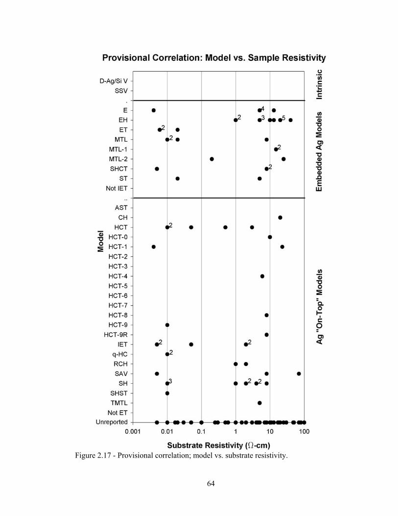
64
Figure 2.17 - Provisional correlation; model vs. substrate resistivity.

65
Figure 2.18 - Null correlation; model vs. substrate preparation temperature.

66
Figure 2.19 - Provisional correlation; model vs. sample preparation temperature.

67
Figure 2.20 - Provisional correlation; model vs. deposition source material.

68
Figure 2.21 - Correlation; model vs. experimental method.
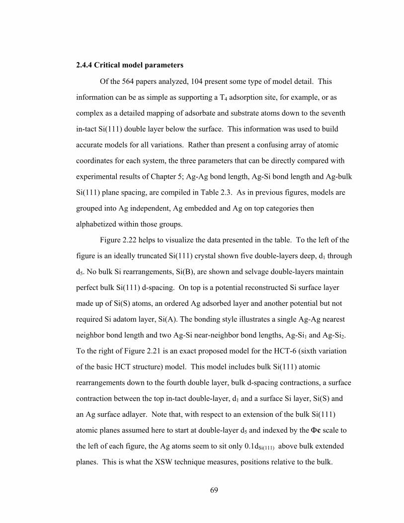
69
2.4.4 Critical model parameters
Of the 564 papers analyzed, 104 present some type of model detail. This
information can be as simple as supporting a T4 adsorption site, for example, or as
complex as a detailed mapping of adsorbate and substrate atoms down to the seventh
in-tact Si(111) double layer below the surface. This information was used to build
accurate models for all variations. Rather than present a confusing array of atomic
coordinates for each system, the three parameters that can be directly compared with
experimental results of Chapter 5; Ag-Ag bond length, Ag-Si bond length and Ag-bulk
Si(111) plane spacing, are compiled in Table 2.3. As in previous figures, models are
grouped into Ag independent, Ag embedded and Ag on top categories then
alphabetized within those groups.
Figure 2.22 helps to visualize the data presented in the table. To the left of the
figure is an ideally truncated Si(111) crystal shown five double-layers deep, d1 through
d5. No bulk Si rearrangements, Si(B), are shown and selvage double-layers maintain
perfect bulk Si(111) d-spacing. On top is a potential reconstructed Si surface layer
made up of Si(S) atoms, an ordered Ag adsorbed layer and another potential but not
required Si adatom layer, Si(A). The bonding style illustrates a single Ag-Ag nearest
neighbor bond length and two Ag-Si near-neighbor bond lengths, Ag-Si1 and Ag-Si2.
To the right of Figure 2.21 is an exact proposed model for the HCT-6 (sixth variation
of the basic HCT structure) model. This model includes bulk Si(111) atomic
rearrangements down to the fourth double layer, bulk d-spacing contractions, a surface
contraction between the top in-tact double-layer, d1 and a surface Si layer, Si(S) and
an Ag surface adlayer. Note that, with respect to an extension of the bulk Si(111)
atomic planes assumed here to start at double-layer d5 and indexed by the Φc scale to
the left of each figure, the Ag atoms seem to sit only 0.1dSi(111) above bulk extended
planes. This is what the XSW technique measures, positions relative to the bulk.

70
Table 2.3 - Summary of bond lengths and bulk registry for Ag/Si(111) models. Model (reference) Ag-Ag
n-n (Å)
Ag-Si 1st n-n
(Å)
Ag-Si 2nd n-n
(Å)
Ag to 1st in-tact DL
(Å)
Ag to bulk registry
d-Si(111) Ag independent models D-Ag/Si V (CN087) random undetermined undetermined 1.38* +0.31* SSV (CN148) random undetermined undetermined ---
* Ag, H3 site and covalent radius assumed Ag embedded models EH (CN065) 3.8402 2.220 2.314 1.4475 ET (CN029) (CN043)
3.0484 2.174 2.787 2.876
3.47
MTL (CN104) 3.8402 2.65 - 3.135 SHCT (CN088) (CN137)
3.3602 2.593 (overlayer)
2.608 2.730 2.778
2.6 +0.96^
ST (CN137) 2.880 2.147 2.540 0.392 ^ from estimates of CN191
Ag on-top models AST (CN145) (CN126)
4.60 1.9919 3.441 4.1775
3.29 +0.05^
AT (CN016) 2.512 3.3 4.084 3.692 CH (CN001) 6.6514 2.9725 3.5432 2.372 HCT (CN016) 4.8121 2.512 3.304 3.994 HCT-1 (CN126) 3.39 2.54 2.68 3.342 HCT-2 (CN139) 2.512 3.30 4.249 3.994 HCT-3 (CN178) 3.39
5.07 2.54 2.63 3.342
HCT-4 (CN202) 3.45 2.54 2.60 3.542 +0.95 HCT-4 (CN185) 3.3742
5.1 2.61 2.721 3.292
HCT-6 (CN241) 3.42 4.98
2.54 2.61 3.532 +0.10
HCT-8 (CN252) 3.426, 4.938 2.593 2.596 3.055 +0.90 HCT-9 (CN275) 3.45 2.41 ? 3.392 +0.96 IET (CN411) 3.0
3.89 2.54 2.60 3.342
q-HC (CN154) (CN162)
2.558 3.840
2.972 3.543 2.072 & 2.372
RCH (CN044) 3.8401 3.8518
2.782 2.972 2.072 2.372
SAV (CN149) 2.88 1.838 2.540 2.985
4.31 +0.93 +0.81^
SH (CN012) 3.8402 2.9725 3.5432 2.372 SHST (CN108) 2.5116 to
2.7691 3.30 4.249 3.342
TMTL (CN142) 3.36 5.38
2.2693 >3 3.342
^ from estimates of CN191

71
Figure 2.22 - Left: ideal surface cross section. Right: exact HCT-6 model with bulk rearrangement, surface contraction & adlayers.

72
2.5 Conclusion
This chapter is the result of an applied study of the question, “Can knowledge
be generated by re-examining and correlating old information in new ways?”. The
question is key to future scientific endeavor where easy access to a vast electronic
library should allow computer aided ‘data mining’. As one who has spent an
inordinate amount of time wandering the stacks of numerous libraries, searching for
relevant information in standard publications as well as obscure conference
proceedings, this author can not wait for the day when it is possible to direct a web-
based system to search for relevant papers by keyword, read them and report back
with correlations based on requested parameters.
From this author’s human driven data mining of the Ag/Si(111) literature base
of almost 600 major papers, the short answer to the question is yes, new knowledge
can be generated. The surface structure diagrams and provisional correlations
presented in this chapter are proof. The practical answer however, is that the majority
of the questions asked will be answered with the phrase, “insufficient information to
complete request”. For every new nugget of knowledge mined from previous research
there are scores of inconclusive, null or insufficient information dead-ends. This
author fears that it will always be more cost effective to generate new information in a
freshly tailored and controlled study if not already researched, rather than try to extract
it from experiments not specifically designed for the question at hand.
In order for the ‘data mining’ concept to be successful, surface scientists must
develop and improve upon the highly successful efforts used in the biological
community; specifically the human genome project and the worldwide protein data
bank, for reporting, storing and accessing surface information. This can only be
accomplished if all surface scientists complete their publication cycle with a “data
reporting” step, wherein extensive, exact and specific details on experimental and

73
theoretical technique are catalogued along with resultant structures or findings. An
excellent start to this process has been made by the Surface Crystallographic
Information Service* in that they require specific experimental and structural details
for an entry to be accepted and catalog the information in a standard format.
As scientists in general, we seem to have forgotten that a publication is not
only a communication with peers, but more importantly is also a “note in a bottle” sent
forward in time to future researchers. Every error and omission profoundly affects
others not yet in the field. For example, looking specifically at the way in which we
acknowledge reference trails, one must acknowledge that each missed or erroneous
reference, each “to be published”, each inclusion of an unrelated publication merely
because it contains your name, wastes the valuable time and talent of scores of others.
The practices are commonplace and yet they must cease. We must imbue ourselves
with the higher ideal of communicating scientific information clearly and concisely
and we must reward the same. Currently, it seems that only the number of referrals or
publications with ones name is the figure of merit and it must also cease.
The success of this endeavor to mine data is shown in the new surface
structural diagram of Figure 2.3 where the ensemble average plot, with all
inconsistencies and ambiguities included, can be used by a scientist skilled in the art,
to surmise new conclusions. The reality of this effort is shown in the correlations of
Sections 2.3 and 2.4 where only inferences rather than solid conclusions are possible.
Inferences may be key but a solid and specific study is still required to firmly link
cause and effect.
* J.M.MacLaren, J.B. Pendry, P.J. Rous, D.K. Saldin, G.A. Somorjai, M.A. Van Hove and D.D. Vvedensky, Surface Crystallographic Information Service: A Handbook of Surface Structures, D. Reidel, Dordrecht 1987.

74
2.6 References – Chapter Two: a chronological record of Ag/Si(111) publications [CNxxx] denotes this author’s ‘Chronological Numbering’ index system
1967 [CN1] K. Spiegel, ''Untersuchungen Zum Schichtwachstum von Silber auf der Silizium(111)-Oberflache Durch Beugung Lansamer Elektronen,'' Surf. Sci. 7, 125-142 (1967).
1969 [CN2] E. Bauer, ''Low Energy Electron Diffraction (LEED) in "Techniques for the Direct Observation of Structure and Imperfections", Techniques Of Metals Research, Vol. II, Part 2, R.F.Bunshah (ed.), Interscience Publishers (John Wiley & Sons), N.Y. 1969, Techniques of Metals Res. 2, 617-621 (1969).
1971 [CN3] A. Hiraki, E. Lugujjo, M.-A. Nicolet, J.W. Mayer, ''Low-Temperature Migration of Silicon through Metal Films Importance of Silicon-Metal Interface,'' Phys. Status Solidi A 7, 401-406 (1971).
1972 [CN4] E. Bauer, H. Poppa, ''Recent Advances in Epitaxy,'' Thin Solid Films 12, 167-185 (1972).
1975 [CN5] A. Thanailakis, ''Contacts Between Simple Metals and Atomically Clean Silicon,'' J. Phys. C 8, 655-668 (1975). [CN6] J.M. Andrews, J.C. Phillips, ''Chemical Bonding and Structure of Metal-Semiconductor Interfaces,'' Phys. Rev. Lett. 35, 56-59 (1975).
1976 [CN7] G. Le Lay, G. Quentel, J.P. Faurie, A. Masson, ''Epitaxy of Noble Metals and (111) Surface Superstructures of Silicon and Germanium II: Study After Annealing,'' Thin Solid Films 35, 289-303 (1976).

75
[CN8] G. Le Lay, G. Quentel, J.P. Faurie, A. Masson, ''Epitaxy of Noble Metals and (111) Surface Superstructures of Silicon and Germanium Part I: Study at Room Temperature,'' Thin Solid Films 35, 273-287 (1976). [CN9] F. Wehking, H. Beckermann, R. Niedermayer, ''Photoemission of Very Thin Ag Layers on (111) Si,'' Thin Solid Films 36, 265-268 (1976). [CN10] J.D. Van Otterloo, J.G. De Groot, ''Relation Between Interface States and Temperature Behavior of the Barrier Height of Silver Contacts on Clean Cleaved n-Type Silicon,'' Surf. Sci. 57, 93-108 (1976). [CN11] G.E. Rhead, ''Probing Surface Properties with Adsorbed Metal Monolayers,'' J. Vac. Sci. Technol. 13, 603-608 (1976).
1977 [CN12] R. Kern, G. Le Lay, ''L'Ordre de Rèaction Zèro dans la Cinètique de Dèsorption Isotherme (ITDS) des Phases 2D Condensèes,'' J. Physique (Colloque C4) 38, 155-163 (1977). [CN13] M. Housley, R. Heckingbottom, C.J. Todd, ''The Interaction of Ag with Si(111),'' Surf. Sci. 68, 179-188 (1977). [CN14] S. Ino, Y. Gotoh, ''A RHEED Study of Si(111) Surface Structures Induced by Ag Evaporation,'' Jpn. J. Appl. Phys. 16, 2261-2262 (1977).
1978 [CN15] G. Le Lay, M. Manneville, R. Kern, ''Cohesive Energy of the Two-Dimensional Si(111)-3x1 Ag and Si(111)√3-R(30°)Ag Phases of the Silver(Deposit)-Silicon(111)(Substrate) System,'' Surf. Sci. 72, 405-422 (1978). [CN16] F. Wehking, H. Beckermann, R. Niedermayer, ''Investigation of the Initial Stages of Growth of Ag Films on Si(111)7x7 by a Combination of LEED,AES and UPS,'' Surf. Sci. 71, 364-374 (1978). [CN17] J. Derrien, G. Le Lay, F. Salvan, ''Electronic and Crystallographic Structures of Silver Adsorbed on Silicon(111),'' J. Physique 39, L287-L290 (1978).

76
[CN18] Y. Gotoh, S. Ino, ''Surface Structures of Ag on Si(111) Surface Investigated by RHEED,'' Jpn. J. Appl. Phys. 17, 2097-2109 (1978).
1979 [CN19] A. McKinley, R.H. Williams, A.W. Parke, ''An Investigation of Thin Silver Films on Cleaved Silicon Surfaces,'' J. Phys. C 12, 2447-2463 (1979). [CN21] R. Kern, G. Le Lay, J.J. Metois, ''"Basic Mechanisms in the early stages of Epitaxy", Chapter 3 in Current Topics in Materials Science, (E. Kaldis, ed.), North-Holland Publishing 3, 132-410 (1979).
1980 [CN22] J.A. Venables, J. Derrien, A.P. Janssen, ''Direct Observation of the Nucleation and Growth Modes of Ag/Si(111),'' Surf. Sci. 95, 411-430 (1980). [CN23] A. Freudenhammer, W. Wönch, P.P. Auer, ''On the Conversion Temperature of Cleaved Stepped Si(111) Surfaces,'' J. Phys. C 12, 4407-4417 (1980). [CN24] V. Barone, G. Del Re, G. Le Lay, R. Kern, ''Adsorption Sites and Relative Stabilities of the 3x1 and √3 Phases of Ag on Si(111),'' Surf. Sci. 99, 223-232 (1980). [CN25] J.P. Gaspard, J. Derrien, A. Cros, F. Salvan, ''Electronic Structure of Ag Adsorbed on Si(111); Experiment and Theory,'' Surf. Sci. 99, 183-191 (1980). [CN26] T. Ichikawa, S. Ino, ''Missing Spots in RHEED Patterns from the Si(111)(6x1)-Ag Surface Structure,'' Surf. Sci. 97, 489-502 (1980). [CN27] L. Braicovich, I. Abbati, J.N. Miller, I. Lindau, S. Schwartz, P.R. Skeath, C.Y. Su, W.E. Spicer,, ''Systematics on the Electron States of Silicon d-Metal Interfaces,'' J. Vac. Sci. Technol. 17, 1005-1008 (1980). [CN28] N. Osakabe, K Yagi, G. Honjo, ''Reflection Electron Microscope Observations of Dislocations and Surface Structure Phase Transition on Clean (111) Silicon Surfaces,'' Jpn. J. Appl. Phys. 19, L309-L312 (1980). [CN29] M. Saitoh, F. Shoji, K. Oura, T. Hanawa, ''Atomic Arrangement of the Si(111)-√3x√3-Ag Structure Derived from Low-Energy Ion Scattering Spectroscopy,'' Jpn. J. 19, L421-L424 (1980). [CN30] K. Yagi, N. Osakabe, Y. Tanishiro, G. Honjo, ''Reflection Electron Microscope Study of Au and Ag Deposited (111) and (001)Si Surfaces in Proceedings of the 4th International Conference on Solid Surfaces and 3rd European Conference

77
on Surface Science, (D.A.Degras and M. Costa, eds.) V.II, Cannes, France,'' Proc.4th Intern. Conf. 2, 1007-1010 (1980). [CN31] T. Hanawa, M. Saito, F. Shoji, K. Oura, ''Surface Structure of Si(111)-√3x√3-Ag as Studied by Low Energy Ion Scattering Spectroscopy in Proceedings of the 4th International Conference on Solid Surfaces and 3rd European Conference on Surface Science, (D.A.Degras and M.Costa, eds.) V.II Cannes, France,'' Proc.4th Intern. Conf. 2, 987-990 (1980). [CN32] D. Bolmont, C. Sebenne, C. Ping, ''Effect of Ag Impurities on the Electronic Properties of the Si(111) Surface in Proceedings of the 4th International Conference on Solid Surfaces and 3rd European Conference on Surface Science, (D.A.Degras and M.Costa, eds.), Vol.II Cannes, France,'' Proc.4th Intern. Conf. 2, 963-966 (1980).
1981 [CN33] G.V. Hansson, R.Z. Bachrach, R.S. Bauer, P. Chiaradia, ''New Models for Metal-Induced Reconstructions on Si(111),'' Phys. Rev. Lett. 46, 1033-1037 (1981). [CN34] K. Oura, T. Taminga, T. Hanawa, ''Electronic Properties and Atomic Arrangement of the Ag/Si(111) Interface,'' Solid State Commun. 37, 523-526 (1981). [CN35] G.V. Hansson, R.Z. Bachrach, R.S. Bauer, P. Chiaradia, ''Electronic and Atomic Structure of Si(111) Al, Ag, and Ni Metal Overlayer Induced Surface Reconstructions,'' J. Vac. Sci. Technol. 18, 550-555 (1981). [CN36] J.D. Van Otterloo, ''Schottky Barriers on Clean-Cleaved Silicon,'' Surf. Sci. 104, L205-L209 (1981). [CN37] T. Narusawa, W.M. Gibson, A. Hiraki, ''Initial Stage of Room-Temperature Metal-Silicide Formation Studied by High-Energy He+-ion Scattering,'' Phys. Rev. B 24, 4835-4838 (1981). [CN38] G. Dufour, J-M. Mariot, A. Masson, H. Roulet, ''Electronic Structure of Ag Two-Dimensional Layers on Si(111): An Electron Spectroscopy Investigation,'' J. Phys. C 14, 2539-2548 (1981). [CN39] D. Bolmont, P. Chen, C.A. Sebenne, F. Proix, ''Structural and Electronic Properties of Cleaved Si(111) Upon Room-Temperature Formation of an Interface with Ag,'' Phys. Rev. B 24, 4552-4559 (1981). [CN40] D. Bolmont, P. Chen, C.A. Sebenne, ''Electronic Properties of the Annealed Interface Between Ag and 7x7Si(111),'' J. Phys. C 14, 3313-3319 (1981).
78
[CN41] A. Cros, F. Salvan, J. Derrien, ''A study of the Si-Au-Ag interface by surface techniques,'' J. Appl. Phys. 52, 4757-4764 (1981). [CN42] Y. Terada, T. Yoshizuka, K. Oura, T. Hanawa, ''Surface Structure of Si(111)-√3x√3-Ag Studies by Averaged LEED Analysis,'' Jpn. J. Appl. Phys. 20, L333-L336 (1981). [CN43] M. Saitoh, F. Shoji, K. Oura, T. Hanawa, ''Initial Growth Process and Surface Structure of Ag on Si(111) Studied by Low-Energy Ion-Scattering Spectroscopy (ISS) and LEED-AES,'' Surf. Sci. 112, 306-324 (1981). [CN44] G. Le Lay, A. Chauvet, M. Manneville, R. Kern, ''The Structural and Electronic Properties of Cleaved Silicon(111) Surfaces Following Adsorption of Silver,'' Appl. Surf. Sci. 9, 190-202 (1981). [CN45] G. Rossi, I. Abbati, L. Braicovich, I. Lindau, W.E. Spicer,, ''Chemical Reaction at the Ge(111)-Ag and Si(111)-Ag Interfaces for Small Ag Coverages,'' Surf. Sci. 112, L765-L769 (1981). [CN46] Y. Gotoh, A. Chauvet, M. Manneville, R. Kern, ''The Effect of Impurity on the Formation of the √3x√3 (R30°) Surface Phase of the Ag-Si(111) System,'' Jpn. J. Appl. Phys. 20, L853-L855 (1981).
1982 [CN47] G. Rossi, I. Abbati, I. Lindau, W.E. Spicer, ''Intermixing at the Early Stage of the Si(111)/Ag Interface Growth,'' Appl. Surf. Sci. 11, 348-354 (1982). [CN48] H. Tokutaka, K. Nishimori, S. Nomura, A. Tanaka, K. Takashima,, ''New Surface Structure Analysis of Ag-Si Phase by Quantitative Auger Electron Spectroscopy Method,'' Surf. Sci. 115, 79-90 (1982). [CN49] Y. Terada, T. Yoshizuka, K. Oura, T. Hanawa, ''A Structure Analysis of Ag-Adsorbed Si(111) Surface by LEED/CMTA,'' Surf. Sci. 114, 65-84 (1982). [CN50] M. Hanbücken, H. Neddermeyer, P. Rupieper, ''Low Energy Electron Diffraction, Auger Electron Spectroscopy and Angle-Resolved Photoemission from Silver Films on Si(100) and Si(111),'' Thin Solid Films 90, 37-42 (1982). [CN51] G. Rossi, L. Caliari, I. Abbati, L. Braicovich, I. Lindau, W.E. Spicer, ''Photoemission Investigation on the Oxidation of Si(111)-Ag Interfaces and its Relation to the Interface Structure,'' Surf. Sci. 116, L202-L206 (1982).

79
[CN52] A. Cros, F. Houzay, G.M. Guichar, R. Pinchaux, ''Passivation of Si(111) Surfaces by Ordered Metal Layers,'' Surf. Sci. 116, L232-L236 (1982). [CN53] P. Muret, ''Capacitance spectroscopy of localized states at metal semiconductor interfaces. II. Experiments about Ag, Au, and Ni on crystalline (111) Si surfaces,'' J. Appl. Phys. 53, 6300-6307 (1982). [CN54] Y. Gotoh, S. Ino, H. Komatsu, ''Effect of Surface Contamination on the Stranski-Krastanov Growth Mode of a Ag/Si System,'' J. Cryst. Growth 56, 498-504 (1982). [CN55] E. Bauer, ''"Chemisorption of Metals on Metals and on Semiconductors" in Interfacial Aspects Of Phase Transformations (B. Mutaftschiev, ed.) Proceedings of the NATO Advanced Study Institute, Erice, Silicy,'' D.Reidel, Holland, 421-431 (1982). [CN56] A. Julg, A. Allouche, ''Theoretical Study of the Adsorption of Silver Atoms on the (111) Face of Silicon,'' Int. J. Quantum Chem. 22, 739-752 (1982). [CN57] J. Stöhr, R. Jaeger, ''Structural Studies of Schottky Barrier Formation by means of Surface EXAFS: Pd and Ag on Si(111)7X7,'' J. Vac. Sci. Technol. 21, 619-623 (1982). [CN58] T. Hoshino, ''Electronic Structures of Chemisorption Systems on Si(111) Surface: II. Si(111)/Ag System,'' Surf. Sci. 121, 1-12 (1982).
1983 [CN59] F. Houzay, G.M. Guichar, A. Cros, F. Salvan, R. Pinchaux, J. Derrien, ''Angle Resolved Photoemission Measurements on Ag-Si(111)7x7 Interfaces,'' Surf. Sci. 124, L1-L8 (1983). [CN60] G. Le Lay, ''Physics and Electronics of the Noble-metal/Elemental Semiconductor Interface formation: A Status Report,'' Surf. Sci. 132, 169-204 (1983). [CN61] T. Yokotsuka, S. Kono, W. Suzuki, T. Sagawa, ''Study of Ag/Si(111) Submonolayer Interface: I. Electronic structure by angle-resolved UPS,'' Surf. Sci. 127, 35-47 (1983). [CN62] K. Horioka, H. Iwasaki, S. Maruno, S. Te Li, S. Nakamura,, ''Ag adsorbed surfaces on Si(111) studied by angle-resolved electron energy loss spectroscopy,'' Solid State Commun. 47, 55-58 (1983).
80
[CN63] G. Le Lay, ''Electronic and atomic structure of Ag-Si(111) and Ag-Ge(111),'' J. Vac. Sci. Technol. B 1, 354-360 (1983). [CN64] Y. Horio, A. Ichimiya, ''Intensity Anomalies of Auger Electron Signals Observed by Incident Beam Rocking Method for Si(111)7x7 and Si(111)√3x√3Ag Surfaces,'' Physica B 117, 792-794 (1983). [CN65] S. Kono, H. Sakurai, K. Higashiyama, T. Sagawa, ''Study of Ag/Si(111) Submonolayer Interface II: Atomic Geometry of Si(111) (√3x√3)R30°-Ag Surface,'' Surf. Sci. 130, L299-L306 (1983). [CN66] J.M. Bermond, J.A. Venables, ''A Model for the Growth Shape of Crystallites on Surfaces,'' J. Cryst. Growth 64, 239-256 (1983). [CN67] Y. Horio, A. Ichimiya, ''RHEED Intensity Analysis of Si(111)7x7 and √3x√3-Ag Surfaces,'' Surf. Sci. 133, 393-400 (1983). [CN68] J. Stöhr, R. Jaeger, G. Rossi, T. Kendelewicz, I. Lindau,, ''Surface Structure of the Ag on Si(111)7X7 Interface by means of Surface EXAFS,'' Surf. Sci. 134, 813-835 (1983). [CN69] Y. Gotoh, S. Ino, ''Epitaxial Growth of Silver on an Si(111) 7x7 Surface at Room Temperature,'' Thin Solid Films 109, 255-261 (1983).
1984 [CN70] K. Horioka, H. Iwasaki, S. Maruno, S-T Li, S. Nakamura,, ''Ag/Si(111)-7x7 Systems Investigated by Angle Resolved Electron Energy Loss Spectroscopy,'' Surf. Sci. 136, 121-132 (1984). [CN71] E.J. Van Loenen, M. Iwami, R.M. Tromp, J.F. van der Veen, ''The Adsorption of Ag on the Si(111) 7x7 Surface at Room Temperature Studied by Medium Energy Ion Scattering, LEED and AES,'' Surf. Sci. 137, 1-22 (1984). [CN72] M. Hanbücken, M. Futamoto, J.A. Venables, ''Growth and diffusion studies of Ag on Si(100) and Si(111) by UHV-SEM and micro-AES; Chapter 4 in Electron Microscopy and Analysis, 1983 (P. Doig, ed.) Proc. Of the Inst. of Phys. Conference, Guildford, The Institute of Physics, Bristol, 1984,'' Electron Microscopy and Anal. 68, 135-138 (1984). [CN73] A.L. Wachs, T. Miller, T.-C. Chiang, ''Angle-resolved photoemission studies of epitaxial Ag films on Si(111)-(7x7),'' Phys. Rev. B 29, 2286-2288 (1984).

81
[CN74] J.A. Venables, G.D.T. Spiller, M. Hanbücken, ''Nucleation and growth of thin films,'' Rep. Prog. Phys. 47, 399-459 (1984). [CN75] M. Hanbücken, M. Futamoto, J.A. Venables, ''Nucleation Growth and the Intermediate Layer in Ag/Si(100) and Ag/Si(111),'' Surf. Sci. 147, 433-450 (1984).
1985 [CN76] S. Nishigaki, K. Takao, T. Yamada, M. Arimoto, T. Komatsu,, ''Metastable-atom Deexcitation Spectroscopy of Clean and Ag-Adsorbed Si(111) Surfaces,'' Surf. Sci. 158, 473-481 (1985). [CN77] M. Futamoto, M. Hanbücken, C.J. Harland, G.W. Jones, J.A. Venables,, ''Visualization of Submonolayers and Surface Topography by Biased Secondary Electron Imaging: Application to Ag Layers on Si and W Surfaces,'' Surf. Sci. 150, 430-450 (1985). [CN78] C. Calandra, O. Bisi, G. Ottaviani, ''Electronic Properties of Silicon-Transition Metal Interface Compounds,'' Surf. Sci. Reports 4, 271-364 (1985). [CN79] C. Elibol, H.-J. Ou, G.G. Hembree, J.M. Cowley, ''Improved instrument for medium energy electron diffraction and microscopy of surfaces.,'' Rev. Sci. Instrum. 56, 1215-1219 (1985). [CN80] G.W. Rubloff, ''Metal-Semiconductor Interfaces and Schottky Barriers in Dynamical Phenomena at Surfaces, Interfaces and Superlattices, F. Nizzoli, K.-H. Rieder and R.F. Willis (eds.), V.3, Springer Surface Science Series,'' Springer Verlag 3, 220-243 (1985). [CN81] S. Hasegawa, S. Ino, Y. Yamamoto, H. Daimon, ''Chemical Analysis of Surfaces by Total-Reflection-Angle X-Ray Spectroscopy in RHEED Experiments (RHEED-TRAXS),'' Jpn. J. Appl. Phys. 24, L387-L390 (1985). [CN82] Y. Horio, A. Ichimiya, ''Surface Structure Study of Si(111)√3x√3-Ag by Incident Beam Rocking AES Method,'' Surf. Sci. 164, 589-601 (1985).
1986 [CN83] C. Jingguang, Z. Kaiming, X. Xide, ''Theoretical studies of the adsorption of Ag on a Si(111) surface,'' Chinese Physics 6, 732-737 (1986).

82
[CN84] J.M. Layet, R. Contini, J. Derrien, H. Lüth, ''Coupled interface plasmons of the Ag-Si(111) system as investigated with high-resolution electron energy-loss spectroscopy,'' Surf. Sci. 168, 142-148 (1986). [CN85] M. Hanbücken, T. Doust, O. Osasona, G. Le Lay, J.A. Venables,, ''SEM Observations of Ag Surface Diffusion at the Si(111)√3-Ag Interface,'' Surf. Sci. 168, 133-141 (1986). [CN86] M. Aono, R. Souda, C. Oshima, Y. Ishizawa, ''Structure Analysis of Ag Overlayers on Si(111) by Low-Energy Li+ Ion Scattering,'' Surf. Sci. 168, 713-723 (1986). [CN87] W.S. Yang, S.C. Wu, F. Jona, ''Structural Reactions of Si1117x7 with Metals,'' Surf. Sci. 169, 383-393 (1986). [CN88] S. Kono, K. Higashiyama, T. Sagawa, ''X-Ray Photoelectron Diffraction Study of the Atomic Geometry of the Si(111)√3x√3-Ag Surface,'' Surf. Sci. 165, 21-36 (1986). [CN89] J.J. Yeh, D.J. Friedman, R. Cao, I. Lindau, ''Summary abstract: Oxidation study of the Si(111) surface with an ordered Ag overlayer,'' J. Vac. Sci. Technol. A 4, 1479-1480 (1986). [CN90] H. Nagayoshi, ''Band structure of Si(111)√3x√3:Ag studied by a mixed-basis pseudopotential method,'' J. Phys. Soc. Jpn. 55, 307-313 (1986). [CN91] A.L. Wachs, A.P. Shapiro, T.C. Hsieh, T.-C. Chiang, ''Observation of film states and surface-state precursors for Ag films on Si(111),'' Phys. Rev. B 33, 1460-1463 (1986). [CN92] Q-G. Zhu, A-D. Zhang, E.D. Williams, R.L. Park, ''On the Detailed Growth Mode of Thin Silver Films on Si(111),'' Surf. Sci. 172, 433-441 (1986). [CN93] V.Y. Aristov, I.L. Boltin, F.A. Grazhulis, V.M. Zhilin, ''LEED and Auger electron spectroscopy study of the Si(111)-2x1+Ag overlayer system in the temperature range 8-300K and coverage range T=0-20 monolayers [original Russian Zh. Eksp. Teor. Fiz. 91, 1411-1425 (1986)],'' Sov. Phys. JETP 64, 832-840 (1986). [CN94] J.A. Venables, ''Nucleation and growth processes in thin film formation,'' J. Vac. Sci. Technol. B 4, 870-873 (1986).

83
[CN95] J.M Nicholls, F. Salvan, B. Reihl, ''Surface States of Ordered Au, Ag and Cu Overlayers on Si(111) Studied by Inverse Photoemission,'' Phys. Rev. B 34, 2945-2948 (1986). [CN96] J.M. Nicholls, F. Salvan, B. Reihl, ''Inverse Photoemission Study of Ordered Cu, Ag, and Au Overlayers on Si(111),'' Surf. Sci. 178, 10-16 (1986). [CN97] J.E. Northrup, ''Origin of Surface States on Si(111)(7x7),'' Phys. Rev. Lett. 57, 154-157 (1986). [CN98] R.G. Wilson, ''The regrowth of implantation damage in silicon studied via silver depth profiling,'' J. Appl. Phys. 60, 2810-2813 (1986). [CN99] H. Tokutaka, K. Nishimori, N. Ishihara, T. Seki, ''A micro-quantitative AES analysis using SEM-SAM apparatus (Applied to Ag/Si interfaces on Si(111)and Si(100) surfaces),'' Jpn. J. Appl. Phys. 25, 1584-1588 (1986). [CN100] A.P. Shapiro, A.L. Wachs, T.C. Hsieh, T. Miller, P. John, T.-C. Chiang, ''Photoemission study of Ag monolayer systems: Effects of the substrate.,'' Phys. Rev. B 34, 7425-7428 (1986).
1987 [CN101] J.-J. Yeh, K.A. Bertness, R. Cao, J. Hwang, I. Lindau,, ''Bonding characteristics of the √3x√3 Ag/Si interface identified by the energy dependence of the photoionization cross section,'' Phys. Rev. B 35, 3024-3027 (1987). [CN102] R.J. Wilson, S. Chang, ''Structure of the Ag/Si(111) Surface by Scanning Tunneling Microscopy,'' Phys. Rev. Lett. 58, 369-372 (1987). [CN103] A.L. Wachs, T. Miller, A.P. Shapiro, T.-C. Chiang, ''Photoemission Studies of the Initial Adsorption and Growth of Ag and Au on Ge and Si,'' Phys. Rev. B 35, 5514-5523 (1987). [CN104] E.J. Van Loenen, J.E. Demuth, R.M. Tromp, R.J. Hamers, ''Local Electron States and Surface Geometry of Si(111)-(√3x√3)Ag,'' Phys. Rev. Lett. 58, 373-376 (1987). [CN105] S. Hasegawa, H. Daimon, S. Ino, ''A Study of Adsorption and Desorption Processes of Ag on Si(111) Surface by Means of RHEED-TRAXS,'' Surf. Sci. 186, 138-162 (1987).

84
[CN106] S. Kono, K. Higashiyama, T. Kinoshita, T. Miyahara, H. Kato, H. Oshawa, Y. Enta, F. Maeda, Y. Yaegashi, ''Surface and Bulk Core-Level Shifts of the Si(111)√3x√3-Ag Surface: Evidence for a Charged √3x√3 Layer,'' Phys. Rev. Lett. 58, 1555-1558 (1987). [CN107] J.A. Venables, ''Nucleation calculations in a pair-binding model,'' Phys. Rev. B 36, 4153-4162 (1987). [CN108] R.J. Wilson, S. Chiang, ''Registration and Nucleation of the Ag/Si(111)(√3x√3)R30 Structure by Scanning Tunneling Microscopy,'' Phys. Rev. Lett. 59, 2329-2332 (1987). [CN109] R.G. Wilson, D.M. Jamba, D.K. Sadana, C.G. Hopkins, ''Range and shape factors, damage, regrowth, and redistribution for Ag implants in (100) and (111) Si,'' J. Appl. Phys. 61, 1355-1358 (1987).
1988 [CN110] J.E. Demuth, E.J. Von Lenen, R.M. Tromp, R.J. Hammers, ''Local electronic structure and surface geometry of Ag on Si(111),'' J. Vac. Sci. Technol. B 6, 18-25 (1988). [CN111] F.K. LeGoues, M. Liehr, M. Renier, W. Krakow, ''Microstructure of epitaxial Ag/Si(111) and Ag/Si(100) interfaces,'' Philos. Mag. B 57, 179-189 (1988). [CN112] S. Ino, ''Experimental Overview of Surface Structure Determination by RHEED in Reflection High-Energy Electron Diffraction And Reflection Electron Imaging Of Surfaces (P.K. Larsen and P.J. Dobson, eds.) Proceedings: NATO Advanced Research Workshop, Veldhoven, Netherlands,'' Plenum Press, 3-28 (1988). [CN113] J.F. McGlip, ''Structure of the Ag/Si Interface in Properties Of Silicon, INSPEC (London),'' EMIS Datareviews Series RN=13928, 725-727 (1988). [CN114] Y. Gotoh, E. Yanokura, ''Growth of Ag crystals on Si(111) surface observed by SEM,'' J. Cryst. Growth 87, 408-414 (1988). [CN115] M. Watamori, T. Nakahara, K. Oura, F. Shoji, T. Hanawa,, ''Structural Changes of Si(100) and (111) Surfaces After Ag Deposition Studied by MeV Ion Channeling,'' Appl. Surf. Sci. 33, 51-57 (1988). [CN116] F. Shoji, T. Kuroi, M. Watamori, K. Oura, T. Hanawa,, ''Capture of Ag atoms in Defects produced by low-energy Ar+ ion bombardment on the Si(111) surface,'' Appl. Surf. Sci. 33, 58-67 (1988).

85
[CN117] S. Kohmoto, A. Ichimiya, ''Adsorption and Desorption of Ag on the Si(111) Surface,'' Appl. Surf. Sci. 33, 45-50 (1988). [CN118] V.A. Grazhulis, ''New Results in Low Temperature Studies of Semiconductor Surfaces,'' Appl. Surf. Sci. 33, 1-14 (1988). [CN119] S. Chiang, R.J. Wilson, Ch. Gerber, V.M. Hallmark, ''An ultrahigh vacuum scanning tunneling microscope with interchangeable samples and tips.,'' J. Vac. Sci. Technol. A 6, 386-389 (1988). [CN120] Q-Q. Zheng, Z. Zeng, R. Han, ''Electronic Structures of Ag-Adsorbed Si(111) Surface,'' Surf. Sci. 195, L173-L181 (1988). [CN121] R.J. Wilson, S. Chiang, ''Image Processing Techniques for Obtaining Registration Information with Scanning Tunneling Microscopy,'' J. Vac. Sci. Technol. A 6, 398-400 (1988). [CN122] R.J. Wilson, S. Chiang, ''Summary Abstract: Scanning Tunneling Microscopy Imaging and Registration of the (√3x√3)R30° Ag/Si(111) Surface,'' J. Vac. Sci. Technol. A 6, 800-801 (1988). [CN123] M. Iwami, M. Kubota, T. Koyama, H. Tochihara, Y. Murata,, ''Resonant-photoemission study of the mechanism for room-temperature-alloyed interface formation of Au and Ag on Si(111)-(2x1),'' Phys. Rev. B 38, 1047-1051 (1988). [CN124] T.L. Porter, C.S. Chang, I.S.T. Tsong, ''Si(111)-(√3x√3) Ag Surface Structure Studied by Impact-Collision Ion-Scattering Spectrometry,'' Phys. Rev. Lett. 60, 1739-1742 (1988). [CN125] St. Tosch, H. Neddermeyer, ''Initial Stage of Ag Condensation on Si(111)7x7,'' Phys. Rev. Lett. 61, 349-352 (1988). [CN126] T. Takahashi, S. Nakatani, N. Okamoto, T. Ishikawa, S. Kikuta,, ''Study on the Si(111)√3x√3-Ag Surface Structure by X-Ray Diffraction,'' Jpn. J. Appl. Phys. 27, L753-L755 (1988). [CN127] A.P. Shapiro, T.C. Hsieh, A.L. Wachs, T. Miller, T.-C. Chiang,, ''Band dispersions of Ag(111) monolayers on various substrates.,'' Phys. Rev. B 38, 7394-7407 (1988). [CN128] K. Oura, M. Watamori, F. Shoji, T. Hanawa, ''Atomic displacements of Si in the Si(111)-(√3x√3)R30°-Ag surface studied by high-energy ion channeling,'' Phys. Rev. B 38, 10146-10148 (1988).

86
[CN129] S-H. Chou, A.J. Freeman, S. Grigoras, T.M. Gentle, B. Delley, E. Wimmer, ''Adsorption of Cu and Ag atoms on Si(111) surfaces: Local density functional determination of geometries and electronic structures.,'' J. Chem. Phys. 89, 5177-5189 (1988). [CN130] St. Tosch, H. Neddermeyer, ''Nucleation and growth of Cu and Ag on Si(111)7x7,'' J. Microsc. 152, 415-422 (1988). [CN131] H. Yasunaga, S. Sakomura, T. Asaoka, S. Kanayama, N. Okuyama, A. Natori, ''Electromigration of Ag ultrathin films on Si(111) 7x7,'' Jpn. J. Appl. Phys. 27, L1603-L1605 (1988). [CN132] T.S. Park, C.I. Chung, S.M. Jung, D.Z. Jeon, ''FIM, RHEED studies on atomatic [sic.] structure of Si(111) and Si(111)-Ag surfaces,'' J. Phys. (Paris) Colloque C6, 275-280 (1988).
1989 [CN133] F. Shoji, M. Watamori, T. Kuroi, K. Oura, T. Hanawa,, ''A study of Ag adsorption on Si(111) surfaces by a compact arrangement of Na+ ISS and LEED,'' J. Phys. D 22, 169-173 (1989). [CN134] M. Ardehali, P.H. Mahowald, I. Lindau, ''Electronic Structure of the Ag/Si Interface: Angle-Resolved, Energy-Dependent, Photoemission Study,'' Phys. Rev. B 39, 8107-8114 (1989). [CN135] M. Jalochowski, E. Bauer, ''RHEED intensity and electrical resistivity oscillations during metallic film growth,'' Surf. Sci. 213, 556-563 (1989). [CN136] K. Markert, P. Pervan, W. Heichler, K. Wandelt, ''Properties of Ultrathin Ag- and Au-Films on Si(111)7x7,'' Surf. Sci. 211, 611-619 (1989). [CN137] E. Vlieg, A.W. Denier van der Gon, H.F. van der Veen, J.E. MacDonald, C. Norris,, ''The Structure of Si(111)-(√3x√3)R30 -Ag Determined by Surface X-Ray Diffraction,'' Surf. Sci. 209, 100-114 (1989). [CN138] C.S. Chang, T.L. Porter, I.S.T. Tsong, ''In-plane geometry of the Si(111)-(√3x√3)Ag surface,'' J. Vac. Sci. Technol. A 7, 1906-1909 (1989). [CN139] T. Takahashi, S. Nakatani, N. Okamoto, T. Ishikawa, S. Kikuta,, ''Studies on Si(111)√3x√3-Bi and -Ag Surfaces by X-ray Diffraction under Nearly Normal Incidence,'' Rev. Sci. Instrum. 60, 2365-2368 (1989).

87
[CN140] F. Salvan, F. Thibaudau, Ph. Dumas, ''STM Studies of Metal-Semiconductor Interface Formation,'' Appl. Surf. Sci. 41, 88-96 (1989). [CN141] E. Vlieg, J.F. van der Veen, ''X-Ray Scattering Studies of Semiconductor Interfaces: Atomic Structure and Morphology,'' Appl. Surf. Sci. 41, 62-69 (1989). [CN142] A. Ichimiya, S. Kohmoto, T. Fujii, Y. Horio, ''RHEED Intensity Analysis of Si(111)√3x√3-Ag Structure,'' Appl. Surf. Sci. 41/42, 82-87 (1989). [CN143] M. Iwami, M. Kusaka, M. Hirai, M. Kubota, H. Tochihara, Y. Murata, ''Mechanism of Alloy Formation due to Noble Metal Deposition on Silicon Surfaces at Room Temperature: Chemical Bonding Model,'' Appl. Surf. Sci. 41, 97-102 (1989). [CN144] K. Sumitomo, K. Tanaka, Y. Izawa, I. Katayama, F. Shoji, K. Oura, T. Hanawa,, ''Structural Study of Ag Overlayers Deposited on a Si(111) Substrate by Impact-Collision Ion-Scattering-Spectroscopy with Time-of-Flight Detection,'' Appl. Surf. Sci. 41, 112-117 (1989). [CN145] R.S. Williams, R.S. Daley, J.H. Huang, R.M. Charatan, ''Initial Stages of Metal/Semiconductor Interface Formation: Au and Ag on Si(111),'' Appl. Surf. Sci. 41/42, 70-74 (1989). [CN146] C.T. Chan, K.M. Ho, ''First Principles Total Energy Calculations for the Honeycomb model of the √3x√3 Ag/Si(111) Surface,'' Surf. Sci. 217, 403-412 (1989). [CN147] G.P. Chambers, B.D. Sartwell, ''Growth Modes of Ag Deposited on Si(111) with Simultaneous Low Energy Ion Bombardment,'' Surf. Sci. 218, 55-74 (1989). [CN148] W.C. Fan, A. Ignatiev, H. Huang, S.Y. Tong, ''Observation and Structural Determination of (√3x√3)R30° Reconstruction of the Si(111) Surface,'' Phys. Rev. Lett. 62, 1516-1519 (1989). [CN149] M. Copel, R.M. Tromp, ''Noble-Metal Adsorption on Si(111): Medium-energy Ion-scattering Results for the Ag(√3x√3)R30° Reconstruction,'' Phys. Rev. B 39, 12688-12694 (1989). [CN150] K. Markert, P. Pervan, W. Heichler, K. Wandelt, ''Structural and electronic properties of Ag/Si(111)and Au/Si(111) Surfaces,'' J. Vac. Sci. Technol. A 7, 2873-2878 (1989). [CN151] H.-S. Jin, K.-H. Park, A.S. Yapsir, G.-C. Wang, T.-M. Lu, L. Luo, W.M. Gibson, I. Yamada, T. Takagi, ''Channeling Study of epitaxial Al and Ag films on Si(111) substrates,'' Nucl. Instrum. Methods B 40, 817-822 (1989).

88
[CN152] R.D. Meade, D. Vanderbilt, ''Adatoms on Si(111) and Ge(111) Surfaces,'' Phys. Rev. B 40, 3905-3913 (1989). [CN153] T. Doust, F.L. Metcalfe, J.A. Venables, ''Biassed Secondary Electron Imaging Studies of Ag/Si(111),'' Ultramicroscopy 31, 116-123 (1989). [CN154] S. Kono, T. Abukawa, N. Nakamura, K. Anno, ''Reinvestigation of the Structure of Si(111)√3x√3-Ag Surface,'' Jpn. J. Appl. Phys. 28, L1278-L1281 (1989). [CN155] S. Kohmoto, A. Ichimiya, ''Determination of the Si(111)"1x1" Structure at High Temperature by Reflection High-Energy Electron Diffraction,'' Surf. Sci. 223, 400-412 (1989). [CN156] L.S.O. Johansson, E. Landemark, D.J. Karlsson, RIG. Uhrberg, ''Fermi-level pinning and surface-state band structure of the Si(111)-(√3x√3R30° -Ag surface,'' Phys. Rev. Lett. 63, 2092-2095 (1989). [CN157] H. Balamane, T. Halicioglu, W.A. Tiller, ''Vacancy- and adatom-induced √3x√3 reconstructions of the Si(111) surface,'' Phys. Rev. B 40, 9999-10001 (1989). [CN158] A. Samsavar, ''Photoemission and Scanning Tunneling Microscopy Investigation of Elemental-Semiconductor Surfaces, Ph.D. Thesis, University of Illinois at Urbana-Champaign, 1989,'' Ph.D. Thesis, 1-179 (1989).
1990 [CN159] J.A. Venables, T. Doust, J.S. Drucker, M. Krishnamurthy, ''Studies of Surface Diffusion and Crystal Growth by SEM and STEM [in Kinetics of Ordering and Growth at Surfaces, Plenum Press, N.Y., 1990, M.G. Lagally (ed.)],'' Plenum Press, 437-453 (1990). [CN160] K.H. Park, G.A. Smith, K. Rajan, G.C. Wang, ''Interface Characterization of Epitaxial Ag Films on Si(100) and Si(111) Grown by Molecular Beam Epitaxy,'' Metall. Trans. A 21, 2323-2332 (1990). [CN161] W.C. Fan, A. Ignatiev, ''Metal-adsorbate-induced Si(111)-(1X3) reconstruction.,'' Phys. Rev. B 41, 3592-3595 (1990). [CN162] S. Kono, Y. Enta, T. Abukawa, N. Nakamura, K. Anno, S. Suzuki, ''VUV and Soft-X-Ray Photoemission Studies of Electronic and Atomic Structures of Metal-Overlayers on Silicon Surfaces,'' Physica Scripta T31, 96-102 (1990).

89
[CN163] M. Watamori, F. Shoji, T. Hanawa, K. Oura, ''High-Energy Ion Channeling Study of the Atomic Displacement of Si(111) Surfaces Induced by Ag Thin Films,'' Surf. Sci. 226, 77-88 (1990). [CN164] C.T. Chan, K.M. Ho, ''Comment on "Observation and Structural Determination of √3x√3R30 Reconstruction of the Si(111) Surface",'' Phys. Rev. Lett. 64, 491-492 (1990). [CN165] G.A. Smith, K.H. Park, G.C. Wang, T.M. Lu, W.M. Gibson,, ''Defect analysis of epitaxial Ag films on silicon by MeV ion channeling,'' Surf. Sci. 233, 115-122 (1990). [CN166] W.C. Fan, A. Ignatiev, ''The effect of surface roughness on reflection high-energy electron diffraction rocking curves and impact on reflection high-energy electron diffraction intensity oscillations.,'' J. Vac. Sci. Technol. A 8, 3479-3483 (1990). [CN167] E.L. Bullock, G.S. Herman, M. Yamada, D.J. Friedman, C.S. Fadley,, ''Structure of (√3x√3)R30° Ag on Si(111),'' Phys. Rev. B 41, 1703-1706 (1990). [CN168] K. Oura, M. Maitoh, J. Yamane, F. Shoji, ''Hydrogen-Induced Reordering of the Si(111)-√3x√3-Ag Surface,'' Surf. Sci. 230, L151-L154 (1990). [CN169] G. Le Lay, M. Abraham, K. Hricovini, J.E. Bonnet, ''Development of Structural and Electronic Properties in the Growth of Metals on Semiconductors [in Kinetics of Ordering and Growth at Surfaces, Plenum Press, N.Y., 1990, M.G. Lagally (ed.)],'' Plenum Press, 209-224 (1990). [CN170] Y. Borensztein, R. Alameh, T. Lopez-Rios, W.Q. Zheng, ''Optical study of Ag overlayers deposited on Si(111)-7x7 as a function of temperature,'' Vacuum 41, 684-686 (1990). [CN171] H. Neddermeyer, ''STM studies of nucleation and the initial stages of film growth” in Critical Reviews in Solid State and Materials Sciences, Crit. Rev. Solid State Mater. Sci 16, 309-335 (1990). [CN172] N. Boutaoui, H. Roux, M. Tholomier, ''Ag mass transport on Si(111) in the 350-450°C temperature range,'' Surf. Sci. 239, 213-221 (1990). [CN173] R.S. Daley, R.M. Charatan, R.S. Williams, ''An investigation of the Si(111)-(√3 x √3)R30°-Ag surface by Li+ impact collision ion scattering spectroscopy,'' Surf. Sci. 240, 136-150 (1990).

90
[CN174] T. Fujikawa, M. Hosoya, ''Theory of Angle-Resolved X-Ray Photoemission by Multiple Scattering Cluster Method. II. Damped One-Electron Formulas Derived from Many-Body Theory and Application to Si(111)-(√3x√3)Ag 3d Spectra,'' J. Phys. Soc. Jpn. 59, 3750-3764 (1990). [CN175] B. Vogt, B. Schmiedeskamp, U. Heinzmann, ''Spin-resolved photoemission from submonolayer Ag on Si(111): Ag adsorption in the (√3x√3)R30° phase with no Ag-Ag interaction and in the 1x1 structure with strong Ag-Ag interaction,'' Phys. Rev. B 42, 9267-9270 (1990). [CN176] A. Samsavar, T. Miller, T.-C. Chiang, ''Correlation between surface core levels and surface states in Si(111)-(7x7) probed by Ag adsorption,'' Phys. Rev. B 42, 9245-9247 (1990).
1991 [CN177] G. Le Lay, M. Abraham, A. Kahn, K. Hricovini, J.E. Bonnet,, ''Abrupt metal-semiconductor interfaces,'' Physica Scripta T35, 261-267 (1991). [CN178] T. Takahashi, S. Nakatani, N. Okamoto, T. Ishikawa, S. Kikuta,, ''A study of the Si(111)√3x√3-Ag surface by transmission X-ray diffraction and X-ray diffraction topography,'' Surf. Sci. 242, 54-58 (1991). [CN179] A. Natori, S. Ohta, H. Yasunaga, ''Structural change of a heterogeneous thin film patch by surface electro-migration.,'' Surf. Sci. 242, 195-201 (1991). [CN180] N-J. Wu, A. Natori, H. Yasunaga, ''Mass transport of a Ag thin film on a stepped Si(111) surface,'' Surf. Sci. 242, 191-194 (1991). [CN181] M. Naitoh, F. Shoji, K. Oura, ''Hydrogen-termination effects on the growth of Ag thin films on Si(111) surfaces,'' Surf. Sci. 242, 152-156 (1991). [CN182] H. Yasunaga, ''Hetero-electromigration on semiconductor surfaces,'' Surf. Sci. 242, 171-180 (1991). [CN183] A. Fortunelli, O. Salvetti, G. Villani, ''Chemisorption of Ag on the Si(111) surface: a theoretical study,'' Surf. Sci. 244, 355-361 (1991). [CN184] I. Kamiya, M. Katayama, E. Nomura, M. Aono, ''Separation of scattered ions and neutrals in CAICISS with an acceleration tube,'' Surf. Sci. 242, 404-409 (1991).

91
[CN185] M. Katayama, R.S. Williams, M. Kato, E. Nomura, M. Aono,, ''Structure Analysis of the Si(111)√3x√3R30°-Ag Surface,'' Phys. Rev. Lett. 66, 2762-2765 (1991). [CN186] K. Takayanagi, ''Restructuring and Symmetry of Surfaces: √3x√3-Ag on Si(111) 7x7 [in The Structure of Surfaces III: Proceedings of the 3rd Int. Conf. on the Structure of Surfaces, Milwaukee, WI, Springer-Verlag, S.Y. Tong, M.A. Van Hove, K. Takayanagi, X.D. Xie (Eds.)],'' Springer Series in Surface Sci 24, 227-236 (1991). [CN187] I. Homma, Y. Tanishiro, K. Yagi, ''Structures Formed by Co-deposition of Two Metals on Si(111)7x7 Studied by Reflection Electron Microscopy [in The Structure of Surfaces III: Proceedings of the 3rd Int. Conf. on the Structure of Surfaces; Tong, Van Hove, Takayanagi, Xie (Eds.)],'' Springer Series in Surf. Sci. 24, 610-614 (1991). [CN188] J.-K. Zuo, J.F. Wendelken, ''Substrate temperature effects on (√3x√3)R30° domain growth of Ag on Si(111) surface,'' Appl. Surf. Sci. 48, 366-372 (1991). [CN189] T.C. Nason, L. You, G.-R. Yang, T.-M. Lu, ''Growth of epitaxial Ag/Si films by the partially ionized beam deposition technique,'' J. Appl. Phys. 69, 773-777 (1991). [CN190] S.Y. Tong, H. Huang, ''The registry of honeycombs in the structure of Si(111)(√3x√3)R30°-Ag,'' Surf. Sci. 243, L46-L48 (1991). [CN191] E. Vlieg, E. Fontes, J.R. Patel, ''Structure analysis of Si(111)-(√3x√3)R30°-Ag using X-Ray standing waves,” Phys. Rev. B 43, 7185-7193 (1991). [CN192] J.-K. Zuo, J.F. Wendelken, ''Defect and impurity effects on the initial growth of Ag on Si(111),'' J. Vac. Sci. Technol. A 9, 1539-1544 (1991). [CN193] D.G. Cahill, R.J. Hamers, ''Surface photovoltage of Ag on Si(111)-7x7 by scanning tunneling microscopy,'' Phys. Rev. B 44, 1387-1390 (1991). [CN194] K. Sumitomo, T. Kobayashi, F. Shoji, K. Oura, I. Katayama,, ''Hydrogen-Mediated Epitaxy of Ag on Si(111) as Studied by Low-Energy Ion Scattering,'' Phys. Rev. Lett. 66, 1193-1196 (1991). [CN195] T.C. Nason, G.-R. Yang, K.-H. Park, T.-M. Lu, ''Study of silver diffusion into Si(111) and SiO2 at moderate temperatures.,'' J. Appl. Phys. 70, 1392-1396 (1991).

92
[CN196] M. Inoue, S. Tanaka, J. Yuhara, K. Morita, ''Ion impact desorption of metal atoms from Si(111)-√3x√3-metal surfaces,'' Nucl. Instrum. Methods B 58, 411-416 (1991). [CN197] G.S. Herman, A.P. Kaduwela, D.J. Friedman, M. Yamada, E.L. Bullock, C.S. Fadley, Th. Lindner, D. Ricken, A.W. Robinson, A.M. Bradshaw, ''Study of (√3x√3)R30° Ag on Si(111) by Photoelectron Diffraction [in The Structure of Surfaces III, Proceedings of the 3rd Int. Conf. on the Structure of Surfaces, Milwaukee, WI, Springer-Verlag, S.Y. Tong, M.A. Van Hove, K. Takayanagi and X.D. Xie (eds.)],'' Springer-Verlag, Berlin 24, 600-605 (1991). [CN198] X. Xide, ''Overview of Metal/Semiconductor Interfaces [in The Structure of Surfaces III: Proceedings of the 3rd Int. Conf. on the Structure of Surfaces, Milwaukee, WI, Springer-Verlag, S.Y. Tong, M.A. Van Hove, K. Takayanagi, X.D. Xie (Eds.)],'' Springer-Verlag, Berlin 24, 576-583 (1991). [CN199] K. Fukutani, H. Daimon, S. Ino, ''Catalytic Effect of Metals (Sn, Ag and Pb) on Homoepitaxial Growth of Ge and Si [in The Structure of Surfaces III: Proceedings of the 3rd Int. Conf. on the Structure of Surfaces, Springer-Verlag, S.Y. Tong, M.A. Van Hove, K. Takayanagi and X.D. Xie (eds.)],'' Springer-Verlag, Berlin 24, 615-622 (1991). [CN200] E. Vlieg, E. Fontes, J.R. Patel, ''Location of Ag in Si(111)-(√3x√3)R30°-Ag from X-Ray Standing Waves in The Structure of Surfaces III: Proceedings of the 3rd Int. Conf. on the Structure of Surfaces, [S.Y. Tong, M.A. Van Hove, K. Takayanagi and X.D. Xie (eds.)],'' Springer-Verlag, Berlin 24, 595-599 (1991). [CN201] J.-K. Zuo, J.F. Wendelken, ''Scaling of the (√3x√3)R30° Domain-Size Distribution with Coverage for Ag/Si(111),'' Phys. Rev. Lett. 66, 2227-2230 (1991). [CN202] Y.G. Ding, C.T. Chan, K.M. Ho, ''Structure of the (√3x√3)R30°Ag/Si(111) Surface from First-Principles Calculations,'' Phys. Rev. Lett. 67, 1454-1457 (1991). [CN203] D.C. McKenna, G.C. Wang, K. Rajan, ''A Diffraction Study of a Heteroepitaxial System-Ag/Si(111),'' J. Electronic Materials 20, 753-758 (1991). [CN204] H. Yasunaga, S. Yoda, ''Driving Force of Electromigration on Semiconductor Surfaces for Ag/Si(111),'' Jpn. J. Appl. Phys. 30, 1822-1825 (1991). [CN205] K. Oura, K. Sumitomo, T. Kobayashi, T. Kinoshita, Y. Tanaka, F. Shoji, I. Katayama,, ''Adsorption of H on Si(111)-√3x√3-Ag: evidence for Ag(111) agglomerates formation,'' Surf. Sci. 254, L460-L464 (1991).

93
[CN206] Y. Tanishiro, K. Takayanagi, K. Yagi, ''Density of silicon atoms in the Si(111)√3x√3-Ag structure studied by in situ UHV reflection electron microscopy,'' Surf. Sci. 258, L687-L690 (1991). [CN207] H. Nagayoshi, ''Surface electronic structure of Si(111),'' Prog. Theor. Phys. 106, 271-279 (1991). [CN208] S. Watanabe, M. Aono, M. Tsukada, ''Theoretical calculations of the scanning-tunneling-microscopy images of the Si(111)√3x√3-Ag surface,'' Phys. Rev. B 44, 8330-8333 (1991). [CN209] G. Raynerd, M. Hardiman, J.A. Venables, ''Temperature-dependent coverage of the √3 x √3R30° structure of Ag/Si(111),'' Phys. Rev. B 44, 13803-13806 (1991). [CN210] M. Huang, E. Hofmann, P. Stenstrom, C.J. Harland, J.A. Venables,, ''Angular resolved electron spectroscopy and imaging of Ag/Si(111) and Ag/Ge(111) [in Electron Microscopy and Analysis, Proc. Inst of Phys. Electron Microscopy and Analysis Group, Conf. Ser.#119, Sect. 3, Bristol, 01-13 Sept. 1991, F.J. Humphreys (ed.)],'' Electron Microscopy and Anal. 119, 147-150 (1991).
1992 [CN211] H. Yasunaga, N.-J. Wu, ''Hetero-electromigration on Stepped Si(111) in Ordering at Surfaces and Interfaces, A. Yoshimori, T. Shinjo and H. Watanabe (eds.), Springer, 1992 (Proc. 3rd NEC Symp., Hakone, Japan Oct. 7-11,1990),'' Ordering at Surf. & Interfaces 17, 263-272 (1992). [CN212] R. Alameh, Y. Borensztein, ''Optical study of oxygen and silver adsorbed on Si(111) surfaces,'' Appl. Surf. Sci. 56, 535-539 (1992). [CN213] N-J. Wu, H. Yasunaga, A. Natori, ''Surface mass transport of Ag and In on vicinal Si(111),'' Surf. Sci. 260, 75-84 (1992). [CN214] G. Raynerd, T.N. Doust, J.A. Venables, ''Competing processes and controlling energies at the Ag/Si(111) interface,'' Surf. Sci. 261, 251-266 (1992). [CN215] S. Watanabe, M. Aono, M. Tsukada, ''First-principles calculation of STM images of the Si(111)√3x√3-Ag surface,'' Ultramicroscopy 42, 105-108 (1992). [CN216] R.J. Cole, J.A. Evans, L. Duò, A.D. Laine, P.S. Fowles, P. Weightman, G. Mondio, D. Norman,, ''Solid-state effects on Ag in dilute alloys revealed by Cooper-minimum photoemission.,'' Phys. Rev. B 46, 3747-3753 (1992).

94
[CN217] H. Hong, R.D. Aburano, D.-S. Lin, H. Chen, T.-C. Chiang, P. Zschack, E.D. Specht,, ''X-Ray Scattering Study of Ag/Si(111) Buried Interface Structures,'' Phys. Rev. Lett. 68, 507-510 (1992). [CN218] R. Schad, S. Heun, T. Heidenblut, M. Henzler, ''Metallic and nonmetallic conductivity of thin epitaxial silver films,'' Phys. Rev. B 45, 11430-11432 (1992). [CN219] T. Kinoshita, Y. Tanaka, K. Sumitomo, F. Shoji, K. Oura, I. Katayama, ''Hydrogen-induced reconstruction of Si(111)-√3-Ag surface studied by TOF-ICISS,'' Appl. Surf. 60, 183-189 (1992). [CN220] S. Watanabe, M. Aono, M. Tsukada, ''Theoretical calculations of the scanning tunneling microscopy images of the Si(111)√3x√3-Ag surface: effects of the tip shape,'' Appl. Surf. Sci. 60, 437-442 (1992). [CN221] H. Yamaguchi, Y. Tanishiro, K. Yagi, ''REM study of surface electromigration of Ge, Au-Cu and Ag on Si(111) surfaces,'' Appl. Surf. Sci. 60, 79-84 (1992). [CN222] H. Yasunaga, N-J. Wu, S. Yoda, T. Aida, K. Sakamoto,, ''Atomic layer control by electromigration on semiconductor surfaces,'' Appl. Surf. Sci. 60, 64-70 (1992). [CN223] L.S.O. Johansson, E. Landemark, C.J. Karlsson, R.I.G. Uhrberg, ''Comment on "Structure of the (√3x√3)R30° Ag/Si(111) Surface from First-Principles Calculations",'' Phys. Rev. Lett. 69, 2451-2452 (1992). [CN224] K.J. Wan, X.F. Lin, J. Nogami, ''Reexamination of the Ag/Si(111)-√3x√3 Surface by Scanning Tunneling Microscopy,'' Phys. Rev. B 45, 9509-9511 (1992). [CN225] S. Hasegawa, S. Ino, ''Surface Structures and Conductance at Epitaxial Growths of Ag and Au on the Si(111) Surface,'' Phys. Rev. Lett. 68, 1192-1195 (1992). [CN226] T.C. Nason, L. You, T.-M. Lu, ''Room temperature epitaxial growth of Ag on low-index Si surface by a partially ionized beam,'' J. Appl. Phys. 72, 466-470 (1992). [CN227] M. Henzler, M. Horn v. Hoegen, U. Kohler, ''Growth of monoatomic layers: Investigations with electron diffraction and scanning tunneling microscopy-Festkorperprobleme,'' Adv. Solid State Phys. 32, 333-353 (1992).

95
[CN228] M. Aono, M. Katayama, E. Nomura, ''Exploring surface structures by coaxial impact collision ion scattering spectroscopy (CAICISS),'' Nucl. Instrum. Methods B 64, 29-37 (1992). [CN229] T. Takahashi, ''Determination of Metal Adsorbed Surfaces by X-Ray Diffraction, in Surface X-Ray And Neutron Scattering, H. Zabel and I.K. Robinson, eds., Springer Verlag (1992),'' Springer Proc. in Physics 61, 11-16 (1992). [CN230] Y. Hwu, M. Marsi, P. Almeras, G. Margaritondo, ''Microscopy Schottky-barrier control: Semiconductor-on-metal case,'' Phys. Rev. B 46, 1835-1837 (1992). [CN231] H. Yasunaga, A. Natori, ''Electromigration on semiconductor surfaces,'' Surf. Sci. Reports 15, 205-280 (1992). [CN232] Y. Borensztein, R. Alameh, ''Optical evidence for interface electronic states at Ag/Si interfaces,'' Surf. Sci. 274, L509-L514 (1992). [CN233] Y.G. Ding, C.T. Chan, K.M. Ho, ''Ding, Chan and Ho Reply to 'Comment on "Structure of the (√3x√3)R30° Ag/Si(111) Surface from First-Principles Calculations" ' by L.S.O. Johansson, E. Landemark, C.J. Karlsson, and R.I.G. Uhrberg. PRL, 69, #16 (1992) 2451.,'' Phys. Rev. Lett. 69, 2452-2452 (1992). [CN234] A. Shibata, Y. Kimura, K. Takayanagi, ''On the restructured layer of the Si(111)√3x√3-Ag structure studied by scanning tunneling microscopy,'' Surf. Sci. 275, L697-L701 (1992). [CN235] M. Naitoh, F. Shoji, K. Oura, ''Direct Observation of the Growth Processes of Ag Thin Film on a Hydrogen-Terminated Si(111) Surface,'' Jpn. J. Appl. Phys. A 31, 4018-4019 (1992). [CN236] A.W. Denier van der Gon, R.M. Tromp, ''Phase Formation Sequence and Domain Structure: A Low-Energy-Electron-Microscopy Study of the Si(111)-(√3x√3)Ag Surface,'' Phys. Rev. Lett. 69, 3519-3522 (1992). [CN237] T. Yamanaka, T. Hanada, S. Ino, H. Daimon, ''Glancing angle dependence of the X-ray emission measured under total reflection angle X-ray Spectroscopy(TRAXS) condition during reflection high energy electron diffraction observation,'' Jpn. J. Appl. Phys. 31, L1503-L1505 (1992). [CN238] K.J. Wan, X.F. Lin, J. Nogami, ''Comparison of the 3x1 reconstructions on the Si(111) surface induced by Li and Ag,'' Phys. Rev. B 46, 13635-13638 (1992).
96
1993 [CN239] A.W. Denier van der Gon, R.M. Tromp, M.C. Reuter, ''Low energy electron microscopy studies of Ge and Ag growth on Si(111),'' Thin Solid Films 236, 140-145 (1993). [CN240] G.S. Herman, E.L. Bullock, M. Yamada, A.P. Kaduwela, D.J. Friedman, S. Thevuthasan, Y.J. Kim, T.T. Tran, C.S. Fadley, Th. Lindner, D.E. Ricken, et.al., ''A Scanned-angle and scanned-energy photoelectron diffraction study of (√3x√3)R30° Ag on Si(111),'' Surf. Sci. 284, 23-52 (1993). [CN241] J.F. Jia, R.G. Zhao, W.S. Yang, ''Atomic structure of the Si(111)(√3x√3)R30°-Ag surface,'' Phys. Rev. B 48, 18109-18113 (1993). [CN242] S. Ino, T. Yamanaka, S. Ito, ''Epitaxial growth of metals on Si and Ge investigated by RHEED-TRAXS and UHV-SEM,'' Surf. Sci. 283, 319-326 (1993). [CN243] S. Hasegawa, S. Ino, ''Surface structures and conductance at initial stages in epitaxy of metals on a Si(111) surface,'' Surf. Sci. 283, 438-446 (1993). [CN244] K.J. Wan, X.F. Lin, J. Nogami, ''Surface reconstructions in the Ag/Si(111) system,'' Phys. Rev. B 47, 13700-13712 (1993). [CN245] H.H. Weitering, J.P. Sullivan, R.J. Carolissen, W.R. Graham, R.T. Tung,, ''Electrical Characteristics of silver/silicon contacts,'' Appl. Surf. Sci. 70, 422-427 (1993). [CN246] S. Chaudhury, R.S. Williams, M. Katayama, M. Aono, ''Quantitative analysis of the azimuthal dependence of ion scattering from Si(111)-(√3x√3)R30°-Ag,'' Surf. Sci. 294, 93-98 (1993). [CN247] M. Sancrotti, L. Duò, R. Cosso, S. D'Addato, D.A. Gregory, P. Unsworth, P. Weightman,, ''l -> (l-1) Ag M(sub)4,5 XAS investigation at the Ag/Si(111) 2x1 interface,'' Appl. Surf. Sci. 70, 456-460 (1993). [CN248] S. Watanabe, M. Aono, M. Tsukada, ''Theoretical calculations of STM images of the Si(111)√3x√3-Ag and -Sb surfaces,'' Surf. Sci. 287, 1036-1040 (1993). [CN249] T. Yamanaka, A. Endo, S. Ino, ''Atomic depth distribution analysis of Ag and Au on Si(111) during epitaxial growth by total reflection angle X-ray spectroscopy,'' Surf. Sci. 294, 53-66 (1993). [CN250] J. Tersoff, A.W. Denier van der Gon, R.M. Tromp, ''Shape Oscillations in Growth of Small Crystals.,'' Phys. Rev. Lett. 70, 1143-1146 (1993).

97
[CN251] R.H. Milne, G.G. Hembree, J.S. Drucker, C.J. Harland, J.A. Venables,, ''Surface studies in UHV SEM and STEM,'' J. Microsc. 170, 193-199 (1993). [CN252] T. Takahashi, S. Nakatani, ''Refinement of the Si(111)√3x√3-Ag structure by surface X-ray diffraction,'' Surf. Sci. 282, 17-32 (1993). [CN253] W.C. Fan, A. Ignatiev, ''Reconstruction of the Si(111)surface induced by alkali metals,'' Surf. Sci. 296, 352-357 (1993). [CN254] A. Shibata, K. Takayanagi, ''Restructuring of the Reconstructed Si(111)7x7 Surface by Metal(Au, Ag) Deposition,'' Jpn. J. Appl. Phys. 32, 1385-1388 (1993). [CN255] K.R. Roos, M.C. Tringides, ''Reflection high-energy-electron-diffraction studies of mass transport and low-temperature growth of Ag/Si(111),'' Phys. Rev. B 47, 12705-12708 (1993). [CN256] S. Heun, J. Bange, R. Schad, M. Henzler, ''Conductance of Ag on Si(111): a two-dimensional percolation problem,'' J. Phys. Condensed Matter 5, 2913-2918 (1993). [CN257] K.R. Roos, M.C. Tringides, ''Flux Dependence of the Ag/Si(111) Growth,'' Europhysics Letters 23, 257-262 (1993). [CN258] H. Ohnishi, I. Katayama, Y. Ohba, F. Shoji, K. Oura,, ''Growth Processes of Si(111)-√3x√3-Ag Studied by Scanning Tunneling Microscope,'' Jpn. J. Appl. Phys. B 32, 2920-2922 (1993). [CN259] C. Ratsch, A. Zangwill, ''Equilibrium theory of the Stranski-Krastanov epitaxial morphology.,'' Surf. Sci. 293, 123-131 (1993). [CN260] T. Sato, T. Sueyoshi, S. Kitamura, M. Iwatsuki, ''Dynamic Observation of Ag Desorption Process on Si(111) Surface by High-Temperature Scanning Tunneling Microscopy,'' Jpn. J. Appl. Phys. B 32, 2923-2928 (1993). [CN261] H. Yamaguchi, T. Ohkawa, K. Yagi, ''Surface electromigration of metal atoms on modified Si(111) surfaces studied by REM,'' Ultramicroscopy 52, 306-311 (1993). [CN262] J. Yuhara, M. Inoue, K. Morita, ''Thermal stability of two-dimensional atomic structures of Au-Ag adsorbates on Si(111) surfaces,'' J. Vac. Sci. Technol. A 11, 2714-2717 (1993).

98
[CN263] G.S. Herman, J.C. Woicik, A.B. Andrews, J.L. Erskine, ''High-resolution photoelectron spectroscopy study of (√3x√3)R30°-Ag on Si(111),'' Surf. Sci. 290, L643-L648 (1993). [CN264] M. Hanbücken, I. Vianey, A. Degiovanni, C. Jourdan, B. Röttger, R. Kliese, H. Neddermeyer,,, ''Plan-view Si(111) samples for surface science and TEM studies,'' Appl. Surf. Sci. 72, 79-88 (1993). [CN265] J.F. Jia, R.G. Zhoa, W.S. Yang, ''Quasikinematic low-energy electron-diffraction surface crystallography,'' Phys. Rev. B 48, 18101-18108 (1993). [CN266] S. Ino, T. Yamanaka, ''Surface atom dynamics in epitaxial growth studied by RHEED-TRAXS,'' Surf. Sci. 298, 432-439 (1993). [CN267] S. Kono, ''Surface-structure analysis by forward scattering in photoelectron and Auger-electron diffraction and by backscattered primary electron diffraction,'' Surf. Sci. 298, 362-368 (1993). [CN268] H. Hasegawa, S. Ino, ''Correlation between atomic-scale structures and macroscopic electrical properties metal-covered Si(111) surfaces,'' Int. J. Modern Phys. 7, 3817-3876 (1993). [CN269] A.A. Saranin, E.A. Khramtsova, V.G. Lifshits, ''Effect on NH3 adsorption on the atomic structure 0f Si(111)√3x√3-Al and Si(111)√3x√3-Ag,'' Surf. Sci. 296, L21-L26 (1993). [CN270] A. Endo, S. Ino, ''Observation of the Ag/Si(111) system using a high-resolution ultra-high vacuum scanning electron microscope,'' Surf. Sci. 293, 165-182 (1993). [CN271] A.A. Saranin, E.A. Khramtsova, V.G. Lifshits, ''Agglomeration of submonolayer Ag films on Si(111) induced by the interaction with atomic hydrogen,'' Surf. Sci. 297, 353-358 (1993). [CN272] Y.G. Ding, C.T. Chan, K.M. Ho, ''The Si(111)-(√3x√3) R30°-Ag and -Au surface structures from first principles calculations,'' Modern Phys. Lett. B 7, 787-795 (1993). [CN273] Y.L. Gavriljuk, V.G. Lifshits, N. Enebish, ''Coadsorption of Au and Ag atoms on the Si(111) surface,'' Surf. Sci. 297, 345-352 (1993).

99
[CN274] A. Endo, ''Observations of Au and Ag coadsorbed Si(111) surfaces by using a high-resolution ultra-high-vacuum scanning electron microscope,'' Surf. Sci. 297, 71-82 (1993). [CN275] H. Over, H. Huang, S.Y. Tong, ''Low-energy electron diffraction as a direct identification technique: Atomic structures of Ag- and Li-induced Si(111)-(√3x√3)R30°,'' Phys. Rev. B 48, 15353-15357 (1993). [CN276] K.D. Leedy, ''Synthesis and Structure of Sputter Deposited Silver-Silicon Films, M.S. Thesis, University of Illinois at Urbana-Champaign, 1993,'' Thesis, 1-62 (1993).
1994 [CN277] V.G.. Lifshits, A.A. Saranin, A.V. Zotov, Surface Phases on Silicon: Preparation, Structures and Properties, John Wiley and Sons, Chichester 1994, Wiley, 55-60 (1994). [CN278] K.R. Roos, M.C. Tringides, ''Low-temperature, flux-independent epitaxy in Ag/Si(111),'' Surf. Sci. 302, 37-48 (1994). [CN279] J. Nogami, K.J. Wan, X.F. Lin, ''Au adatom superstructure on the Ag/Si(111)-√3x√3-R30° surface,'' Surf. Sci. 306, 81-86 (1994). [CN280] E.J. Kirchner, E.J. Baerends, E. Vlieg, ''A study on the Si(111)-√3x√3-Ag system I. Role of the substrate,'' Surf. Sci. 304, 12-23 (1994). [CN281] G. Le Lay, V.Y. Aristov, L. Seehofer, T. Buslaps, R.L. Johnson, M. Göthelid, M. Hammar, U.O. Karlsson, S.A. Flodstrom, R. Feidenhans'l, ''STM and synchrotron radiation studies of "prototypical" metal/semiconductor systems,'' Surf. Sci. 307, 280-294 (1994). [CN282] A. Shibata, Y. Kimura, K. Takayanagi, ''In situ high-temperature STM study of the restructuring process on the Si(111)7x7 surface upon Ag deposition.,'' Surf. Sci. 303, 161-170 (1994). [CN283] H.H. Weitering, N.J. DiNardo, R. Pérez-Sandoz, J. Chen, E.J. Mele,, ''Structural model for the metal-induced Si(111)3x1 reconstruction,'' Phys. Rev. B 49, 16837-16840 (1994). [CN284] A. Shibata, Y. Kimura, K. Takayanagi, ''Restructuring process of the Si(111) surface upon Ag deposition studied by in situ high-temperature scanning tunneling microscopy,'' J. Vac. Sci. Technol. B 12, 2026-2029 (1994).

100
[CN285] P. Müller, R. Kern, A. Ranguis, G. Zerwetz, ''Adsorption Isotherms of Ag/Si(111)7x7,'' Europhysics Letters 26, 461-466 (1994). [CN286] R. Naik, C. Kota, B.U.M. Rao, G.W. Auner, ''Study of epitaxial growth of Ag on hydrogen terminated Si(111) and Si(100) surfaces,'' J. Vac. Sci. Technol. A 12, 1832-1837 (1994). [CN287] E.Z. Luo, S. Heun, M. Kennedy, J. Wollschlager, M. Henzler,, ''Surface roughness and conductivity of thin Ag films,'' Phys. Rev. B 49, 4858-4865 (1994). [CN288] J.A. Venables, R. Persaud, F.L. Metcalfe, R.H. Milne, M. Axim,, ''Rate and diffusion analyses of surface processes,'' J. Phys. Chem. Solids 55, 955-964 (1994). [CN289] S. Hasegawa, Z.H. Zhang, C.S. Jiang, S. Ino, ''Electrical Transport Properties of the Si(111) Surface with Control of Its Atomic-Scale Structure. (in Nanostructures and Quantum Effects: Proceedings of the JRDC International Symposium, Tsukuba, Japan, Nov.1993,Springer-Verlag, H. Sakaki, H. Noge eds.),'' Springer Series in Mat. Sci. 31, 330-340 (1994). [CN290] D.W. McComb, D.J. Moffatt, P.A. Hackett, B.R. Williams, B.F. Mason,, ''Scanning-tunneling-microscopy investigation of the nucleation and growth of Ag/Si(111)-(√3x√3),'' Phys. Rev. B 49, 17139-17148 (1994). [CN291] H. Ohnishi, I. Katayama, Y. Ohba, K. Oura, ''Scanning Tunneling Microscope Observation of Si(111)-3x1-Ag Structure,'' Jpn. J. Appl. Phys. B 33, 3683-3687 (1994). [CN292] J. Nogami, K. Wan, J.C. Glueckstein, ''√3x√3 Reconstructions of Si(111) and Ge(111) Induced by Ag and Au,'' Jpn. J. Appl. Phys. B 33, 3679-3682 (1994). [CN293] M.S. Ashtikar, G.L. Sharma, ''Silver induced formation of Si(111)-√3x√3 structure from hydrogenated amorphous silicon film,'' Solid State Commun. 91, 831-834 (1994). [CN294] G. Meyer, K.H. Rieder, ''Low-temperature scanning tunneling microscopy study of nucleation, percolation, and growth of ultrathin Ag films on Si(111)7x7,'' Appl. Phys. Lett. 64, 3560-3562 (1994). [CN295] B.R. Williams, B.F. Mason, D.W. McComb, D.J. Moffatt, P.A. Hackett,, ''A scanning tunneling microscopy investigation of the reaction of hydrogen atoms with Ag/Si(111)-(√3x√3),'' Surf. Sci. 313, L790-L796 (1994).

101
[CN296] Y. Borensztein, R. Alameh, M. Roy, ''Determination of the morphology of Ag deposits by photoreflectance,'' Phys. Rev. B 50, 1973-1975 (1994). [CN297] J.-K. Zuo, J.F. Wendelken, ''Kinetics of the initial growth for Ag/Si(111),'' Abstract, March APS Meet, J5FrM9- (1994). [CN298] R. Biswas, K. Roos, M.C. Tringides, ''Low-temperature growth on Si(111) substrates,'' Phys. Rev. B 50, 10932-10940 (1994). [CN299] T. Fukuda, ''Determination of silver coverage on Si(111) 3x1(6x1)-Ag surfaces,'' Phys. Rev. B 50, 1969-1972 (1994). [CN300] A. Ichimiya, H. Nomura, Y. Horio, T. Sato, T. Sueyoshi, M. Iwatsuki, ''Formation of √21x√21 structure by gold deposition on Si(111) √3x√3-Ag surface and the wavering behavior.,'' Surf. Rev. and Lett. 1, 1-7 (1994). [CN301] H. Ohnishi, Y. Yamamoto, I. Katayama, Y. Ohba, K. Oura,, ''Hydrogen-Induced Ag Cluster Formation on the Si(111)√3x√3(R30°)-Ag Surface Observed by Scanning Tunneling Microscopy,'' Jpn. J. Appl. Phys. A 33, L1106-L1109 (1994). [CN302] H. Ohnishi, Y. Yamamoto, I. Katayama, Y. Ohba, K. Oura,, ''Scanning tunneling microscope observations of Si(111)3x1-Ag and 6x1-Ag structures,'' Appl. Surf. Sci. 82, 444-448 (1994). [CN303] R. Ishigami, J. Yuhara, K. Morita, ''The change of coverage and structure of the Si(111)-√3x√3-Ag surface by isothermal annealing.,'' Surf. Sci. 321, 100-104 (1994). [CN304] D.W. McComb, R.A. Wolkow, P.A. Hackett, ''Defects on the Ag/Si(111)-(√3x√3) surface,'' Phys. Rev. B 50, 18268-18274 (1994). [CN305] J. Nogami, ''√3x√3 Reconstructions of Si(111) Studied by Scanning Tunneling Microscopy,'' Surf. Rev. and Lett. 1, 395-410 (1994).
1995 [CN306] E.J. Kirchner, E.J. Baerends, G. te Velde, E. Vlieg, ''A study on the Si(111)-√3x√3-Ag system. II. Interaction between substrate and adsorbate,'' Surf. Sci. 330, 113-125 (1995). [CN307] K.R. Kimberlin, M.C. Tringides, ''Flux dependence of in situ electron transport in Ag/Si(111),'' J. Vac. Sci. Technol. A 13, 462-466 (1995).

102
[CN308] J.M. Carpinelli, H.H. Weitering, ''Scanning tunneling microscopy study of the metal-induced Si(111) 3x1 reconstruction: evidence for dimerized chain formation,'' Surf. Sci. 331, 1015-1021 (1995). [CN309] G. Meyer, K.H. Rieder, ''Low temperature STM study on the growth of ultrathin Ag films on Si(111)7x7,'' Surf. Sci. 331, 600-605 (1995). [CN310] R.D. Aburano, H. Hong, J.M. Roesler, D.-S. Lin, T.-C. Chiang, P. Zschack, ''X-ray study of the Ag/Si(111) interface,'' Surf. Sci. 339, L891-L896 (1995). [CN311] J. Yuhara, R. Ishigami, K. Morita, ''Effects of foreign metals on the thermal stability of noble metal adsorbates at the Si(111) surface,'' Surf. Sci. 326, 133-140 (1995). [CN312] H. Ohnishi, Y. Yamamoto, K. Oura, I. Katayama, Y. Ohba,, ''Scanning tunneling microscopy observation of hydrogen-induced Ag cluster formation on the Si(111) surfaces,'' J. Vac. Sci. Technol. A 13, 1438-1442 (1995). [CN313] R.F. Schmitsdorf, T.U. Kampen, W. Mönch, ''Correlation between barrier height and interface structure of Ag/Si(111) Schottky diodes.,'' Surf. Sci. 324, 249-256 (1995). [CN314] T.U. Kampen, R.F. Schmitsdorf, W. Mönch, ''Silver Schottky contacts on Si(111): H-(1x1) surfaces prepared by wet-chemical etching,'' Appl. Phys. A. 60, 391-394 (1995). [CN315] S.A. Parikh, M.Y. Lee, P.A. Bennett, ''Transition metal induced ring-cluster structures on Si(111),'' J. Vac. Sci. Technol. A 13, 1589-1594 (1995). [CN316] T. Yamanaka, S. Ino, ''Atomic depth distribution and growth modes of Ga on Si(111)-2√3 x 2√3-Sn and √3 x √3 -Ag,'' Surf. Sci. 330, 126-134 (1995). [CN317] J. Yuhara, R. Ishigami, D. Ishikawa, K. Morita, ''The interaction of Ni adsorbate with the Ag/Si(111) surface,'' Surf. Sci. 328, 269-276 (1995). [CN318] Z.H. Zhang, S. Hasegawa, S. Ino, ''Reconstruction and growth of Ag on the Si(111)-√3x√3-Ag surface at low temperature,'' Phys. Rev. B 52, 10760-10763 (1995). [CN319] H. Over, S.Y. Tong, J. Quinn, F. Jona, ''Refinement of the Si(111)-(√3x√3)R30°-Ag Structure by Low-Energy Electron Diffraction,'' Surf. Rev. and Lett. 2, 451-457 (1995).

103
[CN320] M. Schleberger, D. Fujita, C. Scharfschwerdt, S. Tougaard, ''Nanostructure of thin metal films on silicon(111) investigated by x-ray photoelectron spectroscopy: Inelastic peak shape analysis,'' J. Vac. Sci. Technol. B 13, 949-953 (1995). [CN321] A. Ichimiya, H. Nomura, Y. Ito, H. Iwashige, ''Gold growth on Si(111)√3x√3Ag and √3x√3Au surfaces,'' J. Cryst. Growth 150, 1169-1174 (1995). [CN322] X.B. Zhang, A.L. Vasiliev, G. Van Tendeloo, Y. He, L.-M. Yu, P.A. Thiry, ''EM. XPS and LEED study of deposition of Ag on hydrogenated Si substrate prepared by wet chemical treatments,'' Surf. Sci. 340, 317-327 (1995). [CN323] R.D. Aburano, H. Hong, J.M. Roesler, K. Chung, D.-S. Lin, P. Zschack, H. Chen, T.-C. Chiang,, ''Boundary-structure determination of Ag/Si(111) interfaces by x-ray diffraction,'' Phys. Rev. B 52, 1839-1847 (1995). [CN324] D.W. McComb, R.A. Wolkow, D.J. Moffatt, P.A. Hackett, ''On the structure and stability of Si(111)-(7x7) fragments created during growth of Ag/Si(111)-(√3x√3),'' Surf. Sci. 340, L955-L959 (1995). [CN325] T. Nakayama, S. Watanabe, M. Aono, ''Structure and stability of the out-of-phase boundary in a surface superlattice, Si(111)√3x√3R30°-Ag,'' Surf. Sci. 344, 143-148 (1995). [CN326] B. Cvikl, T. Mrden, M. Kozelj, D. Korosak, ''Preliminary Investigation of Ag/n-Si(111) Schottky Photodiode Prepared by Ionized-Cluster-Beam Deposition,'' Fizika A 4, 389-395 (1995). [CN327] B. Cvikl, T. Mrden, ''I-V Characteristics of Ionized Cluster Beam Deposited Ag/n-Si(111) Schottky Diode,'' Fizika A 4, 403-411 (1995). [CN328] C. Hwang, C-S. Hwang, C. Lee, S.W. Lee, I-S. Jeong, H.H. Park, S-I. Tanaka, M. Kamada,, ''Fermi-level pinning of Ag in Si(111)-(7x7),'' Phys. Rev. B 52, 16325-16328 (1995).
1996 [CN329] H.H. Weitering, J.P. Sullivan, R.J. Carolissen, R. Pérez-Sandoz, W.R. Graham, R.T. Tung,,, ''Inhomogeneous Schottky barriers at Ag/Si(111) and Ag/Si(100) interfaces,'' J. Appl. Phys. 79, 7820-7829 (1996). [CN330] S. Ino, ''New growth modes and surface conductivity during epitaxy of metals on a Si(111) surface,'' Materials Chem. and Physics 43, 159-165 (1996).

104
[CN331] X. Chen, T. Abukawa, S. Kono, ''Multiple scattering effects on X-ray photoelectron diffraction from Si(111)√3x√3-Ag and -Sb surfaces,'' Surf. Sci. 356, 28-38 (1996). [CN332] A. Endo, S. Ino, ''Energy and angular distribution of secondary electrons emitted from Si(111)-7x7, √3x√3-Ag and 5x2-Au surfaces,'' Surf. Sci. 346, 40-48 (1996). [CN333] K. Oura, H. Ohnishi, Y. Yamamoto, I. Katayama, Y. Ohba,, ''Atomic-hydrogen-induced Ag cluster formation on Si(111)-√3x√3-Ag surface observed by scanning tunneling microscopy,'' J. Vac. Sci. Technol. B 14, 988-991 (1996). [CN334] D. Ishikawa, J. Yuhara, R. Ishigami, K. Soda, K. Morita,, ''Ar+ ion impact desorption of Cu and Ag from the Si(111)-quasi-5x5-Cu and Cu/Si(111)-√3x√3-Ag surfaces,'' Surf. Sci. 356, 59-67 (1996). [CN335] A. Nishiyama, G. ter Horst, P.M. Zagwijn, G.N. van den Hoven, J.W.M. Frenken, F. Garten, A.R. Schlatmann, J. Vrijmoeth,, ''Growth mode and interface structure of Ag on the HF-treated Si(111):H surface,'' Surf. Sci. 350, 229-238 (1996). [CN336] K. Kawamoto, T. Mori, S. Kujime, K. Oura, ''Observation of the diffusion of Ag atoms through an a-Si layer on the Si(111) by low-energy ion scattering,'' Surf. Sci. 363, 156-160 (1996). [CN337] M. Naitoh, A. Watanabe, S. Nishigaki, ''An STM observation of silver growth on hydrogen-terminated Si(111) surfaces,'' Surf. Sci. 357-358, 140-144 (1996). [CN338] D. Ishikawa, J. Yohara, R. Ishigami, K. Soda, K. Morita,, ''Ar+ ion recoil-implantation of Cu and Ag from the Si(111)-quasi-5x5-Cu/Si(111)-√3x√3-Ag surfaces in the keV regime,'' Surf. Sci. 357, 966-970 (1996). [CN339] M. Lijadi, H. Iwashige, A. Ichimiya, ''Silver growth on Si(111)√3x√3-Ag surfaces at low temperature,'' Surf. Sci. 357/358, 51-54 (1996). [CN340] D. Ishikawa, J. Yuhara, R. Ishigami, K. Soda, K. Morita,, ''The interaction of Cu atoms with the Si(111)-√3x√3-Ag surface,'' Surf. Sci. 357, 432-435 (1996). [CN341] X. Chen, T. Abukawa, J. Tani, S. Kono, ''Multiple scattering study of X-ray photoelectron diffraction from Si(111)-√3x√3-Ag surface,'' Surf. Sci. 357, 560-564 (1996). [CN342] A. Natori, M. Murayama, H. Yasunaga, ''Atomic Structures of Ag on √3x√3 Ag/Si(111) and on 7x7 Si(111),'' Surf. Sci. 357, 47-50 (1996).

105
[CN343] R.F. Schmitsdorf, W. Mönch, ''Oxidation of silver-passivated Si(111):Ag-(√3xvR30° surfaces,'' Surf. Sci. 352, 322-326 (1996). [CN344] C-S. Jiang, S. Hasegawa, S. Ino, ''Surface conductivity for Au or Ag on Si(111),'' Phys. Rev. B 54, 10389-10392 (1996). [CN345] T. Nakayama, D.-H. Huang, M. Aono, ''Extraction, deposition, and displacement of atoms by STM,'' Microelectronic Eng. 32, 191-201 (1996). [CN346] F.L. Metcalfe, J.A. Venables, ''Comparisons of Ag deposits on Ge and Si(111),'' Surf. Sci. 369, 99-107 (1996). [CN347] J.M. Carpinelli, H.H. Weitering, ''Low-temperature reconstruction pathway to the Si(111)(√3x√3)R30°-Ag interface,'' Phys. Rev. B 53, 12651-12654 (1996). [CN348] J.C. Woicik, T. Kendelewicz, S.A. Yoshikawa, K.E. Miyano, G.S. Herman, P.L. Cowan, P. Pianetta, W.E. Spicer,, ''Surface-sensitive x-ray standing-wave study of Si(111)√3x√3-Ag,'' Phys. Rev. B 53, 15425-15428 (1996). [CN349] H. Watanabe, M. Ichikawa, ''Development of a multifunctional surface analysis system based on a nanometer scale scanning electron beam: Combination of ultrahigh vacuum-scanning electron microscopy, scanning reflection electron microscopy, Auger electron spectroscopy, and x-ray photoelectron spectroscopy,'' Rev. Sci. Instrum. 67, 4185-4190 (1996). [CN350] Y. Nakajima, G. Uchida, T. Nagao, S. Hasegawa, ''Two-dimensional adatom gas on the Si(111)-(√3x√3)-Ag surface detected through changes in electrical conduction,'' Phys. Rev. B 54, 14134-14138 (1996).
1997 [CN351] Z.H. Zhang, S. Hasegawa, S. Ino, ''RHEED intensity oscillation during epitaxial growth of Ag on Si(111) surfaces at low temperature,'' Phys. Rev. B 55, 9983-9989 (1997). [CN352] C.-S. Jiang, X. Tong, S. Hasegawa, S. Ino, ''Electrical conduction through the surface-state band of the Si(111)-√21x√21-(Ag+Au) structure,'' Surf. Sci. 376, 69-76 (1997). [CN353] P. Pervan, K. Markert, K. Wandelt, ''Photoemission of Xe adsorbed on Si(111)7x7, Ag/Si(111), Au/Si(111) and O/Si(111) surfaces,'' Appl. Surf. Sci. 108, 307-317 (1997).

106
[CN354] K.-H. Park, J.S. Ha, S.-J. Park, El-H. Lee, ''Ag growth on Si(111) with an Sb surfactant investigated by scanning tunneling microscopy,'' Surf. Sci. 380, 258-263 (1997). [CN355] A. Kolmakov, J. Kovac, S. Günther, L. Casalis, L. Gregoratti, M. Marsi, M. Kiskinova,, ''Ag on Au/Si(111): Interfacial interactions on a submicrometer scale,'' Phys. Rev. B 55, 4101-4104 (1997). [CN356] X. Tong, S. Hasegawa, S. Ino, ''Structures and electrical conductance of the Si(111)-√3x√3-Ag surface with additional Ag adsorption at low temperatures,'' Phys. Rev. B 55, 1310-1313 (1997). [CN357] H. Watanabe, M. Ichikawa, ''Structural transformation of hydrogen-adsorbed Si(111)-√3x√3-Ag surfaces induced by electron-stimulated desorption,'' Surf. Sci. 383, 95-102 (1997). [CN358] G. Neuhold, K. Horn, ''Depopulation of the Ag(111)surface state assigned to strain in epitaxial films,'' Phys. Rev. Lett. 78, 1327-1330 (1997). [CN359] T. Okuda, H. Daimon, S. Suga, Y. Tezuka, S. Ino,, ''Surface electronic structure of ordered alkali-and noble metal-overlayers on Si(111),'' Surf. Sci. 121, 89-97 (1997). [CN360] S. Hasegawa, X. Tong, C.-S. Jiang, Y. Nakajima, T. Nagao,, ''Electrical conduction via surface-state bands,'' Surf. Sci. 386, 322-327 (1997). [CN361] M.V. Gomoyunova, I.I. Pronin, N.S. Faradzhev, ''Atomic structure of silver clusters on silicon,'' Tech. Phys. 42, 1429-1432 (1997). [CN362] J.-K. Zuo, J.F. Wendelken, ''Kinetic processes in the transition from Ag(111) crystallites to (√3x√3)R30° domains for Ag/Si(111)-(7x7),'' Phys. Rev. B 56, 3897-3902 (1997). [CN363] J. Yuhara, D. Ishidawa, K. Morita, ''Influence of Ag adsorbate on the Si(111)-√3x√3-(Au,Cu) structure,'' Appl. Surf. Sci. 117, 94-98 (1997). [CN364] K. Kempa, D.A. Broido, H.H. Weitering, ''Correlational switching between 3 x 1 and 6 x 1 surface reconstructions on Si(111) with submonolayer Ag adsorption,'' Physica B 230, 800-802 (1997). [CN365] Y. Ohba, I. Katayama, Y. Yamamoto, M. Watamori, K. Oura,, ''Reconstruction and growth of Ag on hydrogen-terminated Si(111) surfaces,'' Appl. Surf. Sci. 113, 448-452 (1997).

107
[CN366] G. Günther, A. Kolmakov, J. Kovac, M. Marsi, M. Kiskinova,, ''Au on Ag/Si(111)-(√3x√3)R30°: A spectromicroscopy study of a bimetal-silicon interface,'' Phys. Rev. B 56, 5003-5013 (1997). [CN367] Y. Nakajima, S. Takeda, T. Nagao, S. Hasegawa, ''Surface electrical conduction due to carrier doping into a surface-state band on Si(111)-√3x√3-Ag,'' Phys. Rev. B 56, 6782-6787 (1997). [CN368] M.D. Upward, P. Moriarty, P.H. Beton, ''Double domain ordering and selective removal of C60 on Ag/Si(111)-(√3x√3)R30°,'' Phys. Rev. B 56, R1704-R1707 (1997).
1998 [CN369] X. Tong, C.S. Jiang, S. Hasegawa, ''Electronic structure of the Si(111)-√21x√21-(Ag+Au) surface,'' Phys. Rev. B 57, 9015-9023 (1998). [CN370] S. Hasegawa, C.-S. Jiang, Y. Nakajima, T. Nago, X. Tong,, ''Surface Electrical Conduction Correlated with Surface Structures and Atom Dynamics,'' Surf. Rev. and Lett. 5, 803-819 (1998). [CN371] M. Henzler, T. Lüer, A. Burdach, ''Nonmetallic conductivity of epitaxial monolayers of Ag at low temperatures,'' Phys. Rev. B 58, 10046-10053 (1998). [CN372] J. Viernow, M. Henzler, W.L. O'Brien, F.K. Men, F.M. Leibsle, D.Y. Petrovykh, J.L. Lin, F.J. Himpsel,, ''Unoccupied surface states on Si(111)√3x√3-Ag,'' Phys. Rev. B 57, 2321-2326 (1998). [CN373] X. Tong, Y. Sugiura, T. Nagao, T. Takami, S. Takeda, S. Ino, S. Hasegawa,, ''STM observations of Ag adsorption on the Si(111)-√3x√3-Ag surface at low temperatures,'' Surf. Sci. 408, 146-159 (1998). [CN374] D.J. Spence, S.P. Tear, ''STM studies of submonolayer coverages of Ag on Ge(111),'' Surf. Sci. 398, 91-104 (1998). [CN375] K.-H. Park, J.S. Ha, W.S. Yun, E.-H. Lee, ''Ag epitaxial growth on Sb-terminated Si(111) surface,'' Surf. Sci. 405, 46-53 (1998). [CN376] C. Collazo-Davila, D. Grozea, L.D. Marks, ''Determination and refinement of the Ag/Si(111)-(3x1) surface structure,'' Phys. Rev. Lett. 80, 1678-1681 (1998). [CN377] M. Riehl-Chudoba, Wo. Richter, V.A. Gasparov, ''Scanning tunneling microscope induced nanostructuring of a Si(111)/Ag(√3x√3)R30°surface,'' J. Appl. Phys. 83, 2500-2503 (1998).

108
[CN378] L. Huang, S.J. Chey, J.H. Weaver, ''Buffer-layer-assisted growth of nanocrystals: Ag-Xe-Si(111),'' Phys. Rev. Lett. 80, 4095-4098 (1998). [CN379] K. Akimoto, M. Lijadi, S. Ito, A. Ichimiya, ''Interface Structure and Preferred Orientation of Ag/Si(111) Revealed by X-ray Diffraction,'' Surf. Rev. and Lett. 5, 719-722 (1998). [CN380] J. Yuhara, K. Morita, ''Thermal reaction processes of ternary metal (Au, Ag, Cu) adsorbates on the Si(111) surface,'' Appl. Surf. Sci. 123, 56-60 (1998). [CN381] D. Ishikawa, J. Yuhara, K. Soda, K. Morita, ''Ion impact desorption of binary noble metal adsorbates on the Si(111) surface,'' Nucl. Instrum. Methods B 135, 314-318 (1998). [CN382] K. Pedersen, C. Tomas, P. Morgen, ''Deposition and Growth of Ag on Si(111) Surfaces Studied by Optical Second-harmonic Generation,'' Surf. Interface Anal. 26, 872-875 (1998). [CN383] B. Cvikl, D. Korosak, Zs.J. Horváth, ''Comparative study of I-V characteristics of the ICB deposited Ag/n-Si(111) and Ag/p-Si(100) Schottky junctions,'' Vacuum 50, 385-393 (1998). [CN384] M.D. Upward, P. Moriarty, P.H. Beton, P.R. Birkett, H.W. Kroto, D.R.M. Walton, R. Taylor,, ''Functionalized fullerenes on silicon surfaces,'' Surf. Sci. 405, L526-L531 (1998). [CN385] K. Miki, K. Sakamoto, T. Sakamoto, ''Surface preparation of Si substrates for epitaxial growth,'' Surf. Sci. 406, 312-327 (1998). [CN386] S. Jay Chey, L. Huang, J.H. Weaver, ''Manipulation and writing with Ag nanocrystals on Si(111)-7x7,'' Appl. Phys. Lett. 72, 2698-2700 (1998). [CN387] L. Huang, S. J. Chey, J.H. Weaver, ''Metastable structures and critical thicknesses: Ag on Si(111)-7x7,'' Surf. Sci. 416, L1101-L1106 (1998). [CN388] S.C. Erwin, H.H. Weitering, ''Theory of the "Honeycomb Chain-Channel" reconstruction of M/Si(111)-(3x1),'' Phys. Rev. Lett. 81, 2296-2299 (1998). [CN389] G. Le Lay, M. Göthelid, A. Cricenti, C. Håkansson, P. Perfetti,, ''Atomic origins of the Si 2p surface core-level shifts of th4 "prototypical" Si(111)√3x√3 R(30°)-Ag structure,'' Europhysics Letters 45, 65-70 (1998).

109
[CN390] S. Jay Chey, L. Huang, J.H. Weaver, ''Self-assembly of multilayer arrays from Ag nanoclusters delivered to Ag(111) by soft landing,'' Surf. Sci. 419, L100-L106 (1998).
1999 [CN391] S. Hasegawa, X. Tong, S. Takeda, N. Sato, T. Nagao,, ''Structures and electronic transport on silicon surfaces,'' Prog. Surf. Sci. 60, 89-257 (1999). [CN392] B. Sundaravel, A.K. Das, S.K. Ghose, K. Sekar, B.M. Dev,, ''Epitaxial growth of silver on Br-passivated Si(111) substrates under high vacuum,'' Appl. Surf. Sci. 137, 11-19 (1999). [CN393] A.A. Saranin, A.V. Zotov, V.G. Lifshits, M. Katayama, K. Oura,, ''Family of the metal-induced Si(111)3x1 reconstructions with a top Si atom density of 4/3 monolayer,'' Surf. Sci. 426, 298-307 (1999). [CN394] L. Gavioli, K.R. Kimberlin, M.C. Tringides, J.F. Wendelken, Z. Zhang,, ''Novel growth of Ag islands on Si(111): Plateaus with a singular Height,'' Phys. Rev. Lett. 82, 129-132 (1999). [CN395] T. Nagao, S. Ohuchi, Y. Matsuoka, S. Hasegawa, ''Morphology of ultrathin manganese silicide on Si(111),'' Surf. Sci. 419, 134-143 (1999). [CN396] A.A. Saranin, A.V. Zotov, V.G. Lifshits, J.-T. Ryu, O. Kubo, H. Tani, T. Harada, M. Katayama, K. Oura, ''Ag-induced structural transformations on Si(111):quantitative investigation of the Si mass transport,'' Surf. Sci. 429, 127-132 (1999). [CN397] N. Sato, S. Takeda, T. Nagao, S. Hasegawa, ''Electron standing waves on the Si(111)-√3x√3-Ag surface,'' Phys. Rev. B 59, 2035-2039 (1999). [CN398] S. Jay Chey, L. Huang, J.H. Weaver, ''Interface bonding and manipulation of Ag and Cu nanocrystals on Si(111)-(7x7)-based surfaces,'' Phys. Rev. B 59, 16033-16041 (1999). [CN399] T. Minobe, T. Uchihashi, T. Tsukamoto, S. Orisaka, Y. Sugawara, S. Morita, ''Distance dependence of noncontact-AFM image contrast on Si(111)√3x√3-Ag structure,'' Appl. Surf. Sci. 140, 298-303 (1999). [CN400] M. Henzler, T. Lüer, J. Heitman, ''Magnetoconductivity of ultrathin epitaxial Ag films on Si(111)7x7 at low temperatures,'' Phys. Rev. B 59, 2383-2387 (1999).

110
[CN401] Y. Sugawara, T. Minobe, S. Orisaka, T. Uchihashi, T. Tsukamoto, S. Morita, ''Non-contact AFM Images Measured on Si(111)√3x√3-Ag and Ag(111) Surfaces,'' Surf. Interface Anal. 27, 456-461 (1999). [CN402] S. Kitamura, K. Suzuki, M. Iwatsuki, ''High resolution imaging of contact potential difference using a novel ultrahigh vacuum non-contact atomic force microscope technique,'' Appl. Surf. Sci. 140, 265-270 (1999). [CN403] S.R. Blankenship, H.H. Song, A.A. Baski, J.A. Carlisle, ''Reconstructions of Ag on high-index silicon surfaces,'' J. Vac. Sci. Technol. A 17, 1615-1620 (1999). [CN404] K. Fukutani, H. Iwai, Y. Murata, H. Yamashita, ''Hydrogen at the surface and interface of metals on Si(111),'' Phys. Rev. B 59, 13020-13025 (1999). [CN405] T. Nakayama, J. Onoe, K. Takeuchi, M. Aono, ''Weakly bound and strained C60 monolayer on the Si(111)√3x√3R30°-Ag substrate surface,'' Phys. Rev. B 59, 12627-12631 (1999). [CN406] H. Aizawa, M. Tsukada, ''First-principles study of Ag adatoms on the Si(111)-√3x√3-Ag surface,'' Phys. Rev. B 59, 10923-10927 (1999). [CN407] G. Le Lay, J.M. Layet, A. Cricenti, C. Ottaviani, P. Perfetti,, ''Spectroscopic signatures of a symmetry-breaking surface phase transition: Ag/Si(111)√3x√3->3x1,'' Surf. Sci. 438, 97-101 (1999). [CN408] Y. Suzuki, H. Minoda, N. Yamamoto, ''STM light emission from Ag/Si(111),'' Surf. Sci. 438, 297-304 (1999). [CN409] M. Henzler, O. Pfennigtorf, K. Lang, T. Lüer, F. Moresco, T. Hildebrandt, ''Structure and electronic properties of epitaxial metallic monolayers,'' Surf. Sci. 438, 178-184 (1999). [CN410] C-S. Jiang, S. Hasegawa, ''Photoconductivity of te Si(111)-7x7 and √3x√3-Ag surfaces,'' Surf. Sci. 427, 239-244 (1999). [CN411] H. Aizawa, M. Tsukada, N. Sato, S. Hasegawa, ''Asymmetric structure of the Si(111)-√3x√3-Ag surface,'' Surf. Sci. 429, L509-L514 (1999). [CN412] N. Sato, T. Nagao, S. Hasegawa, ''Si(111)-(√3x√3)-Ag surface at low temperatures: symmetry breaking and surface twin boundaries,'' Surf. Sci. 442, 65-73 (1999).

111
[CN413] H. Nienhaus, H.S. Bergh, B. Gergen, A. Majundar, W.H. Weinberg, E.W. McFarland, ''Selective H atom sensors using ultrathin Ag/Si Schottky diodes,'' Appl. Phys. Lett. 74, 4046-4048 (1999). [CN414] M.D. Upward, P.H. Beton, P. Moriarty, ''Adsorption of cobalt phthalocyanine on Ag terminated Si(111),'' Surf. Sci. 441, 21-25 (1999).
[CN415] K. Yokoyama, T. Ochi, Y. Sugawara, S. Morita, ''Atomically resolved silver imaging on the Si(111)- (√3x√3)-Ag surface using a noncontact atomic force microscope,'' Phys. Rev. Lett. 83, 5023-5026 (1999).
[CN416] K. Tsuchie, T. Nagao, S. Hasegawa, ''Structure of C60 layers on the Si(111)-√3x√3-Ag surface,'' Phys. Rev. B 60, 11131-11136 (1999). [CN417] K. Oura, V.G. Lifshits, A.A. Saranin, A.V. Zotov, M. Katayama,, ''Hydrogen interaction with clean and modified silicon surfaces,'' Surf. Sci. Reports 35, 1-74 (1999). [CN418] N. Sato, T. Nagao, S. Hasegawa, ''Two-dimensional adatom gas phase on the Si(111)-√3x√3-Ag surface directly observed by scanning tunneling microscopy,'' Phys. Rev. B 60, 16083-16087 (1999). [CN419] T.G. Pedersen, K. Pedersen, T.B. Kristensen, ''Optical second-harmonic generation from Ag quantum wells on Si(111)7x7:Experiment and theory,'' Phys. Rev. B 60, R13997-R14000 (1999). [CN420] H. Hirayama, H. Okamoto, K. Takayanagi, ''Growth of high-density small Ag islands on the Si(111)7x7 surface with adatom defects,'' Phys. Rev. B 60, 14260-14264 (1999). [CN421] S. Morita, Y. Sugawara, S. Orisada, T. Uchihashi, ''Missing Ag atom on Si(111)√3x√3-Ag surface observed by noncontact atomic force microscopy,'' Jpn. J. Appl. Phys. 38, L1342-L1344 (1999). [CN422] D. Grozea, E. Bengu, C. Collazo-Davila, L.D. Marks, ''Structure Determination of the Ge(111)-(3x1)Ag Surface Reconstruction,'' Surf. Rev. and Lett. 6, 1061-1065 (1999).

112
2000 [CN423] X. Tong, T. Shiokawa, K. Hammura, Y. Aoyagi, ''Erratum to: "Scanning tunneling microscopy evidence of a special bonding of Cu adatoms on Si(111)-√3x√3-Ag surface. Direct observation of surface-state electron migration." [Surface Science 446 (2000) 120-126],'' Surf. Sci. 457, 294-294 (2000). [CN424] A. Hata, K. Akimoto, S. Horii, T. Emoto, A. Ichimiya, H. Tajiri, T. Takahashi, H. Sugiyama, X. Zhang, H. Kawata, ''Crystal orientation of silver films on silicon surfaces (Session 15B2/2000S2-003),'' Abstract of AIP March Meeting, S2-003- (2000). [CN425] T.G. Pedersen, K. Pedersen, T.B. Kristensen, ''Optical second-harmonic generation as a probe of quantum well states in ultrathin Au and Ag films deposited on Si(111),'' Thin Solid Films 364, 86-90 (2000). [CN426] H. Wang, J.G. Hou, O. Takeuchi, Y. Fujisuku, A. Kawazu,, ''STM observations of Ag-induced reconstruction of C60thin films,'' Phys. Rev. B 61, 2199-2203 (2000). [CN427] X. Tong, T. Shiokawa, K. Hammura, Y. Aoyagi, ''Scanning tunneling microscopy evidence of a special bonding of Cu adatoms on Si(111)√3x√3-Ag surface Direct observation of surface-state electron migration,'' Surf. Sci. 446, L120-L126 (2000). [CN428] X. Tong, C-S. Jiang, K. Horikoshi, S. Hasegawa, ''Surface-state electrical conduction on the Si(111)-√3 x √3-Ag surface with noble-metal adatoms,'' Surf. Sci. 449, 125-134 (2000). [CN429] D.K. Sarkar, S. Dhara, K.G. Nair, S. Chowdhury, ''Studies of phase formation and chemical states of the ion beam mixed Ag/Si(111) system,'' Nucl. Instrum. Methods B 168, 215-220 (2000). [CN430] N. Sasaki, H. Aizawa, M. Tsukada, ''Fourier expansion method for noncontact atomic force microscopy image simulations-Application to Si(111)√3x√3-Ag surface,'' Jpn. J. Appl. Phys. 39, L174-L177 (2000). [CN431] F. Moresco, M. Rocca, T. Hildebrandt, M. Henzler, ''Growth of ultrathin nanostructured Ag films on Si(111) 7x7:a SPA-LEED study,'' Surf. Sci. 463, 22-28 (2000). [CN432] F. Shi, I. Shiraki, T. Nagao, S. Hasegawa, ''Substrate-Structure Dependence of Ag Electromigration on Au-Precovered Si(111) Surfaces,'' Jpn. J. Appl. Phys. 39, 4438-4442 (2000).

113
[CN433] N. Sasaki, H. Aizawa, M. Tsukada, ''Theoretical simulation of noncontact AFM images of Si(111) √3x√3-Ag surface based on Fourier expansion method,'' Appl. Surf. Sci. 157, 367-372 (2000). [CN434] P. Sobotík, I. Ost'ádal, J. Myslivecek, T. Jarolímek, ''STM study of nucleation of Ag on Si(111)-(7x7) at submonolayer coverage,'' Surf. Sci. 454-456, 847-850 (2000). [CN435] D.K. Sarkar, S. Dhara, KGM. Nair, S. Chowdhury, ''Surface morphology of the Ar+ ion-irradiated Ag/Si(111) system,'' Nucl. Instrum. Methods B 170, 413-418 (2000).
[CN436] M. Yoon, H. Mai, G. Lee, R.F. Willis, ''Stabilizing influence of double bonds on the Si(111)-(3x1) and Ge(111)-(3x1) surface reconstructions: new experimental evidence,'' Surf. Sci. 463, 183-190 (2000).
[CN437] S. Hasegawa, N. Sato, I. Shiraki, C.L. Petersen, P. Boggild, T.M. Hansen, T. Nagao, F. Grey,, ''Surface-State Bands on Silicon--Si(111)-√3x√3-Ag Surface Superstructure--,'' Jpn. J. Appl. Phys. 39, 3815-3822 (2000). [CN438] K.-J. Jin, B.C. Sanders, S.-H. Pan, G.-Z. Yang, ''Quantum size effects in metal-induced Si(111) surface reconstructions,'' Surf. Sci. Letters 464, L739-L744 (2000).
2001 [CN439] K. Pedersen, T.B. Kristensen, T.G. Pedersen, Per Morgen, Z. Li, S.V. Hoffmann, ''Optical second-harmonic generation and photoemission from quantum well states in thin Ag films on Si(111),'' Surf. Sci. 482-485, 735-739 (2001). [CN440] J. Yuhara, K. Soda, K. Morita, ''Adsorption of Ag on the Si(111)√3x√3-Au surface.,'' Surf. Sci. 482-485, 32-38 (2001). [CN441] T. Jarolímek, J. Myslivecek, P. Sobotík, I. Ost'ádal, ''Adsorption and diffusion of Ag atoms on Si(111)-(7x7) surface.,'' Surf. Sci. 482-485, 386-390 (2001). [CN442] D, Korosak, B. Cvikl, ''The microscopic model of Fermi level pinning in ionized cluster beam deposited Ag/n-Si Schottky structures.,'' Vacuum 61, 349-353 (2001).

114
[CN443] J. Myslivecek, P. Sobotík, I. Ost'ádal, T. Jarolímek, ''Unconventional features of Ag epitaxy on the Si(111) 7x7 surface,'' Phys. Rev. B 63, 045403-1-045403-5 (2001). [CN444] B.N. Cotier, M.D. Upward, F.H. Jones, P. Moriarty, P.H. Benton,, ''Atomic scale protection using fullerene encapsulation,'' Appl. Phys. Lett. 78, 126-128 (2001). [CN445] H. Hirayama, T. Komizo, T. Kawata, K. Takayanagi, ''Optical second harmonic generation spectrum of Ag/Si(111) reconstructed surfaces,'' Phys. Rev. B 63, 155413-1-155413-5 (2001). [CN446] Y. Nakamura, Y. Kondo, J. Nakamura, S. Watanabe, ''Theoretical study on the structural phase transition of Si(111)√3x√3-Ag surface,'' Surf. Sci. 493, 206-213 (2001). [CN447] S. Horii, K. Akimoto, S. Ito, T. Emoto, A. Ichimiya, H. Tajiri, W. Yashiro, S. Nakatani, T. Takahashi, H. Sugiyama, et.al, ''Interface reconstructed structure of Ag/Si(111) revealed by X-ray diffraction,'' Surf. Sci. 493, 194-199 (2001). [CN448] N. Sasaki, S. Watanabe, H. Aizawa, M. Tsukada, ''Simulation of interaction force between Si tip and Si(111)√3x√3-Ag surface of IET structure in noncontact AFM,'' Surf. Sci. 493, 188-193 (2001). [CN449] K. Kakitani, A. Yoshimori, H. Aizawa, M. Tsukada, ''Theoretical analyses of phase transition and Debye-Waller factor of Si(111)-Ag√3x√3 surface,'' Surf. Sci. 493, 200-205 (2001). [CN450] Y. Oshima, H. Nakade, S. Shigeki, H. Hirayama, K. Takyanagi,, ''UHV-TEM/TED observation of Ag islands grown on Si(111)√3x√3-Ag surface,'' Surf. Sci. 493, 366-372 (2001). [CN450.5] S. Kagami, H. Minoda, N. Yamamoto, ''STM light emission from Si(111)√3x√3-Ag surface,'' Surf. Sci. 493, 78 (2001). [CN451] H. Tajiri, K. Sumitani, W. Yashiro, S. Nakatani, T. Takahashi, K. Akimoto, H. Sugiyama, X. Zhang, H. Kawata, ''Structural study of Si(111)√21x√21-(Ag+Au) surface by X-ray diffraction,'' Surf. Sci. 493, 214-220 (2001). [CN452] K. Sakamoto, H. Ashima, H.M. Zhang, R.I.G. Uhrberg, ''Identification of the basic structure of the Ag/Si(111)-(6 x 1) surface: Observation of a low-temperature c(12 x 2) phase.,'' Phys. Rev. B 65, 045305-1-045305-8 (2001).
115
[CN453] B. Cvikl, D. Korosak, ''The effective density of induced interface states of ionized cluster beam deposited Ag/n-Si Schottky junctions.,'' Vacuum 61, 355-359 (2001). [CN454] Y. Nakamura, Y. Kondo, J. Nakamura, S. Watanabe, ''STM Images Apparently Corresponding to a Stable Structure: Considerable Fluctuation of a Phase Boundary of the Si(111)-(√3x√3)-Ag Surface.,'' Phys. Rev. Lett. 87, 156102-1-156102-4 (2001). [CN455] H. Hirayama, T. Kawata, K. Takayanagi, ''Oscillation of the optical second-harmonic generation intensity during Ag thin film growth on a Si(111)7x7 surface.,'' Phys. Rev. B 64, 195415-1-195415-5 (2001). [CN456] X. Tong, S. Ohuchi, N. Sato, T. Tanikawa, T. Nagao, I. Matsuda, Y. Aoyagi, S. Hasegawa,, ''Electronic structure of Ag-induced √3x√3 and √21x√21 superstructures on the Si(111) surface studied by angle-resolved photoemission spectroscopy and scanning tunneling microscopy.,'' Phys. Rev. B 64, 205316-1-205316-9 (2001). [CN457] H.M. Zhang, K. Sakamoto, R.I.G. Uhrberg, ''Comprehensive study of the metal/semiconductor character of adatom-induced Ag/Si(111) reconstructions.,'' Phys. Rev. B 64, 245421-1-245421-4 (2001).
2002 [CN458] I. Matsuda, H.W. Yeom, ''Study of the quantum-well states in ultra-thin silver films on Si surfaces (Journal of Electron Spectroscopy and Related Phenomena),'' J. Electron Spect. 126, 101-115 (2002). [CN459] H.M. Zhang, K. Sakamoto, R.I.G. Uhrberg, ''Semiconductor-metal-semiconductor transition: valence band photoemission study of Ag/Si(111) surfaces.,'' Appl. Surf. Sci. 190, 103-107 (2002). [CN460] X. Tong, S. Ohuchi, T. Tanikawa, A. Harsawa, T. Okuda, Y. Aoyagi, T. Kinoshita, S. Hasegawa,, ''Core-level photoemission of the Si(111)-√21 x √21-Ag surface using synchrotron radiation.,'' Appl. Surf. Sci. 190, 121-128 (2002). [CN461] H. Hirayama, T. Komizo, T. Kawata, K. Takayanagi, ''Changes of phase and intensity of optical SHG with Ag deposition on Si(111)-7x7 surfaces,'' Appl. Surf. Sci. 190, 108-112 (2002). [CN461.2] N. Kishi, K. Morita, '' Differential scattering cross-sections, inelastic energy losses and ion fractions in backscattering of keV He+ ions from monolayer

116
metal adsorbates on solid surfaces measured by means of CAICISS,'' Nucl. Inst. Meth. Phys. B 193, 419 - 432 (2002). [CN461.5] M. Fonin, J.M. Choi, U. May, J.O. Hauch, U. Rüdiger, G. Güntherodt, ''Low temperature formation of Si(111)-(2n+1)x(2n+1) surface reconstructions,'' Surf. Sci. 1-3, 312 (2002). [CN462] A. Arranz, J.F. Sánchez-Royo, J. Avila, V. Pérez-Dieste, P. Dumas, M.C. Asensio, ''Electronic properties and Fermi surface of Ag(111) films deposited onto H-passivated Si(111)-(1 x 1) surfaces.,'' Phys. Rev. B 65, 075405-1-075405-10 (2002). [CN462.2] J.F. Sánchez-Royo, J. Avila, V. Pérez-Dieste, M. De Seta, M.C. Asensio, ''Two-domains bulklike Fermi surface of Ag films deposited onto Si(111)-(7x7),'' Phys. Rev. B 66, 035401-1 - 035401-9 (2002). [CN462.5] S. Morita, Y. Sugawara, '' Mapping and control of atomic force on Si(111)√3x√3-Ag surface using noncontact atomic force microscope,'' Ultramicroscopy 91, 89 - 96 (2002). [CN463] Y. Oshima, H. Nakade, S. Shigeki, H. Hirayama, K. Takayanagi,, ''Commensurate and incommensurate striped structure of Ag film growth on Si(111)√3x√3 surface at room temperature.,'' Surf. Sci. 498, 307-313 (2002). [CN464] A. Arranz, J.F. Sánchez-Royo, J. Avila, V. Pérez-Dieste, P. Dumas, M.C. Asensio, ''Quantum-well states in ultrathin Ag(111) films deposited onto H-passivated Si(111)-(1 x 1) surfaces.,'' Phys. Rev. B 65, 195410-1-195410-7 (2002). [CN465] N. Sasaki, S. Watanabe, M. Tsukada, ''Visualization of Thermally Fluctuating Surface Structure in Noncontact Atomic-Force Microscopy and Tip Effects on Fluctuation: Theoretical Study of Si(111)-(√3x√3)-Ag Surface,'' Phys. Rev. Lett. 88, 046106-1-046106-4 (2002). [CN465.5] L. Chen, Y. Zheng, P. Nyugen, T.L. Alford, ''Silver diffusion and defect formation in Si(111) substrate at elevated temperatures,'' Mat. Chem. Phys. 76, 224 (2002). [CN466] I. Matsuda, T. Ohta, H.W. Yeom, ''In-plane dispersion of the quantum-well states of the epitaxial silver films on silicon.,'' Phys. Rev. B 65, 085327-1-085327-7 (2002). [CN467] Y. Takagi, A. Nishimura, A. Nagashima, J. Yoshino, ''Formation of iron silicide nanodots on Si(111)-√3x√3Ag,'' Surf. Sci. 514, 167-171 (2002).

117
[CN468] J.M. Zuo, B.Q. Li, ''Nanostructure Evolution During Cluster Growth: Ag in H-Terminated Si(111) Surfaces,'' Phys. Rev. Lett. 88, 25502-1-25502-4 (2002). [CN469] S. Glass, E.W. McFarland, H. Nienhaus, ''Structural changes on the nano-meter scale of thin Ag films on Si(111) surfaces by NO exposure.,'' Surf. Sci. 518, 133-140 (2002). [CN470] H. Hirayama, T. Yamaguchi, H. Ikezawa, K. Tanaka, ''Influence of 1X1 defects on Schottky barrier height at the Ag/Si(111) 7X7 interface.,'' Phys. Rev. B 66, 073301-1-073301-4 (2002).
[CN471] R. Venkataraghavan, M. Aono, T. Suzuki, ''Studies on the nucleation, dynamics and structure of the Si(111)-√3x√3-Ag surface using surface second-harmonic generation.,'' Surf. Sci. 517, 65-74 (2002).
[CN472] C.-S. Jiang, H. Yu, C.-K. Shih, Ph. Ebert, ''Effect of the SI substrate structure on the growth of two-dimensional thin Ag films.,'' Surf. Sci. 518, 63-71 (2002). [CN472.5] P. Sobotík, I. Ost'ádal, P. Kocán, ''Reconstruction determined submonolayer growth of Ag on Si(111)-(7x7) surface,'' Surf. Sci. 507-510, 389 (2002). [CN473] J.N. Crain, K.N. Altmann, C. Bromberger, F.J. Himpsel, ''Fermi surfaces of surface states on Si(111)-Ag,Au,'' Phys. Rev. B 66, 205302-1-205302-8 (2002). [CN474] V.U. Nazarov, S. Nishigaki, T. Nagao, ''Nonlinear mechanism of plasmon damping in electron gas.,'' Phys. Rev. B 66, 092301-1-092301-4 (2002). [CN475] B.W. Li, J.-M. Zuo, ''The development of epitaxy of nanoclusters on lattice-mismatched substrates: Ag on H-Si(111) surfaces.,'' Surf. Sci. 520, 7-17 (2002). [CN476] W.X. Tang, K.L. Man, H. Huang, C.H. Woo, M.S. Altman, ''Growth shapes of Ag crystallites on the Si(111) surface,'' J. Vac. Sci. Technol. B 20, 2492 - 2495 (2002). [CN477] M. Gurnett, J.B. Gustafsson, K.O. Magnusson, S.M. Widstrand, L.S.O. Johansson,, ''Angle-resolved photoemission study of the single-domain Si(111)(3X1)/(6X1)-Ag surface,'' Phys. Rev. B 66, 161101-1-161101-4 (2002).

118
[CN478] J. Kuntze, A. Mugarza, J.E. Ortega, ''Ag-induced zero- and one-dimensional nanostructures on vicinal Si(111),'' Appl. Phys. Lett. 81, 2463 - 2465 (2002). [CN479] K. Onishi, T. Kumakura, D. Fujita, '' Nanostructure fabrication for future nanodevices using a scanning tunneling microscope,'' Superlattices and Microstruct. 32, 249 - 253 (2002).
2003 [CN480]A. Hata, K. Akimoto, S. Horii, T. Emoto, A. Ichimiya, H. Tajiri, T. Takahashi, H. Sugiyama, X. Zhang, H. Kawata, ''Crystal Orientation of Silver Films on Silicon Surfaces Revealed by Surface X-ray Diffraction,'' Surf. Rev. Lett. 10, 431 (2003). [CN481] J. Jiao, M.H. Pan, Q.K. Xue, X.H. Bao, '' Oxygen-induced migration of Ag nano-clusters on Si(111)-7x7 surface,'' Chinese J. Catalysis 24, 433 - 436 (2003). [CN482] T. Yamanaka, N. Shimomura, S. Ino, ''Direct observation of growth motion of elements by ultrahigh vacuum scanning electron microscopy combined with total reflection angle x-ray spectroscopy,'' Surf. Interface Anal. 35, 2 - 6 (2003). [CN483] J. Kovac, '' Spectromicroscopic study of bimetal/semiconductor interfaces by synchrotron light,'' Vacuum 71, 3 - 10 (2003). [CN484] T. Müller, H. Nienhaus, ''Ultrathin Ag films on H:Si(111)-1x1 surfaces deposited at low temperatures,'' J. Appl. Phys. 93, 924-930 (2003). [CN485] P. Sobotík, I. Ostádal, P. Kocán, J. Myslivecek, T. Jarolímek, ''Reconstruction-determined diffusion of Ag adatoms on the Si(111)-(7x7) surface,'' Czech. J. Physics 53, 69 - 74 (2003). [CN486] K. Márquez, G. Staikov, J.W. Schultze, '' Silver deposition on silicon and glassy carbon. A comparative study in cyanide medium.,'' Electrochem. Acta 48, 875 - 882 (2003). [CN487] Y. Nakamura, H. Koga, S. Watanabe, ''Multistage Order-Disorder Surface Transition of Si(111)√3x√3-Ag Surface with Defects,'' J. Phys. Soc. Jpn. 72, 13 - 16 (2003). [CN488] J.K. Bording, B.Q. Li, Y.F. Shi, J.M. Zuo, ''Size- and Shape-Dependent Energetics of Nanocrystal Interfaces: Experiment and Simulation.,'' Phys. Rev. Lett. 90, 226104-1-226104-4 (2003).

119
[CN489] D. Fujita, K. Onishi, T. Kumakura, ''Silver Nanostructures Formation on Si(111)-(7 x 7) Surfaces by the Tip of a Scanning Tunneling Microscope,'' Jpn. J. Appl. Phys. 42, 4773-4776 (2003). [CN490] H. Tajiri, K. Sumitani, S. Nakatani, A. Nojima, T. Takahashi, K. Akimoto, H. Sugiyama, X. Zhang, H. Kawata, ''X-ray diffraction study of the Si(111) -√3x√3-Ag surface structure.,'' Phys. Rev. B 68, 035330-1-035330-5 (2003). [CN491] D. Fujita, T. Kumakura, ''Reproducible fabrication of metallic silver nanostructures on a Si(111)-(7x7) surface by tip-material transfer of a scanning tunneling microscope,'' Appl. Phys. Lett. 82, 2329 - 2331 (2003). [CN492] P. Sobotík, P. Kocán, I. Ost'ádal, ''Direct observation of Ag intercell hopping on the Si(111)-(7x7) surface,'' Surf. Sci. 537, L442 (2003). [CN493] I. Ostádak, P. Kocán, J. Myslivecek, P. Sobotík, ''Ag/Si(111)-(7x7) heteroepitaxy - STM experiment and KMC simulations,'' Czech. J. Phys. 53, 41 - 48 (2003). [CN494] Ph. Guaino, D. Carty, G. Hughes, P. Moriarty, A.A. Cafolla, '' Scanning tunneling microscopy study of pentacene adsorption on Ag/Si(111)-(√3x√3)R30°,'' Appl. Surf. Sci. 212-213, 537 - 541 (2003). [CN495] H. Hirayama, A. Yamasaki, T. Kawata, '' Change of optical second harmonic generation intensity during Ag deposition on Si(111)7x7 and Si(111)√3x√3-Ag surfaces,'' Surf. Sci. 532-535, 922 - 927 (2003). [CN496] T. Takahashi, H. Tajiri, K Sumitani, K. Akimoto, H. Sugiyama, X. Zhang, H. Kawata, ''X-ray diffraction study of the phase transition of the Si(111)(√3x√3)-Ag surface,'' Surf. Rev. Lett. 10, 519 - 524 (2003). [CN497] T. Uchihashi, Urs Ramsperger, '' Atomic-scale characterization of metal micro-electrodes grown on clean semiconductor surfaces,'' Thin Solid Films 438, 61 - 64 (2003). [CN498] M. Ueno, I. Matsuda, C. Liu, S. Hasegawa, ''Step Edges as Reservoirs of Ag Adatom Gas on a Si(111) Surface,'' Jpn. J. Appl. Phys. 42, 4894-4897 (2003). [CN499] H. Hirayama, A. Yamasaki, T. Kawata, ''Change of optical second harmonic generation intensity during Ag deposition on Si(111)7x7 and Si(111)√3x√3-Ag surfaces,'' Surf. Sci. 532-535, 922 (2003).

120
[CN500] B.Q. Li, J.M. Zuo, ''Self-assembly of epitaxial Ag nanoclusters on H-terminated Si(111) surfaces,'' J. Appl. Phys. 94, 743 - 748 (2003). [CN501] V. Pérez-Dieste, J.F. Sanchez, M. Izquierdo, L. Roca, J. Avila, M.C. Asensio, ''The growth of silver films on Si(111)-(7x7) studied by using photoelectron diffraction,'' Appl. Surf. Sci. 212-213, 235 (2003). [CN502] K. Thürmer, E.D. Williams, J.E. Reutt-Robey, ''Dewetting dynamics of ultrathin silver films on Si(111),'' Phys. Rev. B 68, 155423-1 - 155423-7 (2003). [CN503] J.N. O'Shea, M.A. Phillips, M.D.R. Taylor, P.H. Beton, P. Moriarty, M. Kanai, T.J.S. Dennis, V.R. Dhanak, S. Patel, N. Poolton, ''Competing interactions of noble metals and fullerenes with the Si(111)7x7 surface,'' J. Chem. Phys. 119, 13046-13052 (2003). [CN504] D.K. Aswal, K.P. Muthe, N. Joshi, A.K. Debnath, S.K. Gupta, J.V. Yakhmi, ''In situ X-ray photoelectron spectroscopy of Ag/Al bilayers grown by molecular beam epitaxy,'' J. Cryst. Growth 256, 201 - 205 (2003). [CN505] I. Matsuda, H. Morikawa, C. Liu, S. Ohuchi, S. Hasegawa, T. Okuda, T. Kinoshita, C. Ottaviani, A. Cricenti, M. D'angelo, et.al., ''Electronic evidence of asymmetry in the Si(111) √3x√3-Ag structure.,'' Phys. Rev. B 68, 085407-1-085407-5 (2003). [CN506] M. Dávila, J. Avila, M.C. Asensio, G. Le Lay, ''Complex Behaviors at Simple Semiconductor and Metal/Semiconductor Surfaces,'' Surf. Rev. Lett. 10, 981 (2003). [CN507] S. Hasegawa, I. Shiraki, F. Tanabe, R. Hobara, T. Kanagawa, T. Tanikawa, I. Matsuda, C.L. Petersen, T.M. Hansen, P. Boggild &F.Grey, ''Electrical conduction through surface superstructures measured by microscopic four-point probes,'' Surf. Rev. Lett. 10, 963 - 980 (2003). [CN508] K. Pedersen, P. Morgen, ''Second-harmonic generation spectroscopy on reconstructed Si(111) surfaces,'' Phys. Stat. Sol. 0, 3065 - 3069 (2003). [CN509] L Pizzagalli, A. Baratoff, ,''Theory of single atom manipulation with a scanning probe tip: Force signatures, constant-height, and constant-force scans,'' Phys. Rev. B 68, 115427-1 (2003). [CN510] K.R. Kimberlin, G.M. Rutter, L.M. Nagle, K.R. Roos, M.C. Tringides, ''Annealing of low-temperature growth in Ag/Si(111) as measured by RHEED spot profile analysis,'' Surf. Interface Anal. 35, 1069 - 1072 (2003).

121
[CN511]D. Adams, B.A. Julies, J.W. Mayer, T.L. Alford, ''The effect of metals (Au, Ag) and oxidizing ambient on interfacial reactions in Au/Si and Ag/Si systems,'' Appl. Surf. Sci. 216, 163 (2003). [CN512] Ph Guaino, A.A. Cafolla, O. McDonald, D. Carty, G. Sheerin, G. Hughes, ''Scanning tunnelling spectroscopy of low pentacene coverage on the Ag/Si(111)-(√3x√3) surface,'' J. Phys. Condens. Matter 15, S2693 - S2698 (2003). [CN513] T. Yamanaka, ''Atomic depth distribution analysis and growth dynamics of metals on metal-covered Si(111) surfaces studied by incident-angle-dependent RHEED-TRAXS (total-reflection-angle x-ray spectroscopy),'' e-J. Surf. Sci. Nanotech. 1, 91 - 101 (2003).
2004 [CN514] M. Goto, N. Nakata, F. Honda, '' Tribological behavior of an Ag subnanometer-thick film on an Si(111)7x7 surface at elevated temperatures,'' Wear 256, 726 - 734 (2004). [CN515] X-J. Liang, J-L. Li, X. Liu, J-Z. Wang, H. Liu, Q-K. Xue, J-F. Jia, ''Spontaneous assembly of ordered nanoclusters and nanowires,'' Surf. Interface. Anal. 36, 100 - 103 (2004). [CN516] P. Sobotík, I. Ost'ádal, P. Kocán, ''STM observation of Ag adatom interactions on the Si(111)-(7x7) surface,'' Vacuum 76, 465 (2004). [CN517] P. Kocán, P. Sobotík, I. Ost'ádal, M Kotrla, ''Continuous and correlated nucleation during nonstandard island growth at Ag/Si(111)-7X7 heteroepitaxy.,'' Phys. Rev. B 69, 165409-1-165409-6 (2004). [CN518] M. Cinchetti, D.A. Valdaitsev, A. Gloskovskii, A. Oelsner, S.A. Nepijko, G. Schönhense, '' Photoemission time-of-flight spectromicroscopy of Ag nanoparticle films on Si(111),'' J. Elect. Spect. Rel. Phenom. 137-140, 249 - 257 (2004). [CN519] D. Deng, T. Suzuki, ''Si(111)-3x1-Ag Reconstruction Studied In Situ at Elevated Temperatures by Second-Harmonic Generation,'' Jpn. J. Appl. Phys. 43, L510 - L512 (2004). [CN520] A. Keffous, M. Siad, A. Cheriet, N. Benrekaa, Y. Belkacem, H. Menari, W. Chergui, A. Dahmani, '' Comparison of electrical and optical parameters of Au/n-Si and Ag/n-Si Schottky barrier photodiodes,'' Appl. Surf. Sci. 236, 42 - 49 (2004).

122
[CN521] V. Pantín, J. Avila, M.E. Dávila, J.E. Bonnet, M.C. Asensio, '' Photoelectron diffraction study of Ag growth mediated by an arsenic layer on Si(111)1x1,'' J. Elect. Spect. Rel. Phenom. 137-140, 155 - 160 (2004). [CN522] S.V. Ryjkov, M.V. Lavrinaitis, D.A. Tsukanov, V.G. Lifshits, '' Stability and electric conductivity of Si-metal surface reconstructions during amorphous Si deposition,'' Appl. Surf. Sci. 237, 119 - 124 (2004). [CN523] R.I.G. Uhrberg, H.M. Zhang, '' High-resolution photoemission studies of adsorbates and overlayers on semiconductor surfaces,'' J. Elect. Spect. Rel. Phenom. 137-140, 205 - 210 (2004). [CN524] B. Satpati, P.V. Satyam, T. Som, B.N. Dev, ''Nanoscale ion-beam mixing in Ag-Si and Ag-Si eutectic systems,'' Appl. Phys. A 79, 447 - 451 (2004). [CN525] R.A. Zhachuk, S.A. Tiis, B.Z. Ol'shanetskii, ''Formation of Silver Nanodots and Nanowires on a Si(557) Surface,'' JETP Lett. 79, 381 - 382 (2004). [CN526] L. Wang, K. Schulte, R.A.J. Woolley, M. Kanai, T.J.S. Dennis, J. Purton, S. Patel, S. Gorovikov, V.R. Dhanak, E.F. Smith, et. al., '' Morphology, structure, and electronic properties of Ce@C82 films on Ag:Si(111)-(√3x√3)R30°,'' Surf. Sci. 564, 156 - 164 (2004). [CN527] 625 H.M. Zhang, K. Sakamoto, R.I.G. Uhrberg, ''Surface electronic structure of K- and Cs-induced √21x√21 phases on Ag/Si(111)√3x√3,'' Phys. Rev. B 70, 245301-1 - 245301-7 (2004). [CN528] V. Pantín, J. Avila, M.E. Dávila, J.E. Bonnet, M.C. Asensio, ''Photoelectron diffraction study of Ag growth mediated by an arsenic layer on Si(111) 1x1,'' J. Electron. Spectrosc. 137-140, 155 (2004). [CN529] K. Takahiro, K. Kawatsura, S. Nagata, S. Yamamoto, H. Naramoto, ''Irradiation-induced improvement in crystal quality of epitaxial Ag/Si(111) films,'' J. Appl. Phys. 96, 4166 - 4170 (2004). [CN530] I. Matsuda, M. Ueno, T. Hirahara, R. Hobara, H. Morikawa, C. Liu, S. Hasegawa, ''Electrical Resistance of a Monatomic Step on a Crystal Surface,'' Phys. Rev. Lett. 93, 236801-1 - 236801-4 (2004). [CN531] R.A. Zhachuk, S.A. Teys, A.E. Dolbak, B.Z. Olshanetsky, '' Formation of ordered arrays of Ag nanowires and nanodots on Si(557) surface,'' Surf. Sci. 565, 37 - 44 (2004).

123
[CN532] T. Hirahara, I. Matsuda, M. Ueno, S. Hasegawa, ''The effective mass of a free-electron-like surface state of the Si(111)√3x√3-Ag surface investigated by photoemission and scanning tunneling spectroscopies,'' Surf. Sci. 563, 191 (2004). [CN533] P. Kocán, P. Sobotík, I. Ost'ádal, M. Kotrla, ''Self-organized growth of Ag islands on Si(111)-(7x7)-optimization of an STM experiment by means of KMC simulations,'' Surf. Sci. 566-568, 216 (2004). [CN534] H. Nakahara, T. Suzuki, A. Ichimiya, ''Ag/Si(111)√3x√3 surface phase transition at low temperature studied by RHEED,'' Appl. Surf. Sci. 234, 292 (2004). [CN535] D.H. Wei, C.C. Yu, S.C. Chou, Y.D. Yao, Y. Liou, T.S. Chin, ''Ag buffer layer effect on magnetization reversal of epitaxial Co films,'' Phys. Stat. Sol. (a) 201, 361 - 3365 (2004). [CN536] D. Deng, M. Numata, T. Suzuki, ''Kinetics of Excess Ag Atoms on Si(111)-√3x√3-Ag Studied by Second-Harmonic Generation,'' J. Phys. Soc. Jpn. 73, 3384 - 3388 (2004). [CN537] L. Chen, H.J. Xiang, B. Li, A. Zhao, X. Xiao, J. Yang, J.G. Hou, Q. Zhu, ''Detecting surface resonance states of Si(111)-√3x√3-Ag with a scanning tunneling microscope,'' Phys. Rev. B 70, 245431-1 - 245431-5 (2004).
2005 [CN538] J-M. Zuo, B. Li, '' Nanocluster interfaces and epitaxy, Ag on Si surfaces,'' Zeits. Metall. 96, 438 - 442 (2005). [CN539] C. Liu, I. Matsuda, S. Hasegawa, ''Scanning tunnelling microscopy observations at initial stage of Cs adsorption on Si(111)-√3x√3-Ag surface,'' Surf. Interface Anal. 37, 101 - 105 (2005). [CN540] K. Vanormelingen, K. Paredis, A. Vantomme, ''Fe-silicide nanostructures on Si(111)-√3x√3-Ag,'' J. Appl. Phys. 98, 024302-1 - 024302-5 (2005). [CN541] H. Jeong, S. Jeong, ''Diffusion of Ag adatom on the H-terminated and clean Si(111) surfaces: A first-principles study,'' Phys. Rev. B 71, 035310-1 - 035310-7 (2005). [CN542] W.B. Su, H.Y. Lin, Y.P. Chiu, H.T. Shih, T.Y. Fu, Y.W. Chen, C.S. Chang, T.T. Tsong, ''Correlation between morphological transition and preferred thickness of Pb and Ag islands on Si(111)7x7,'' Phys. Rev. B 71, 073304-1 - 073304-4 (2005).

124
[CN543] M. Escher, N. Weber, M. Merkel, C. Ziethen, P. Bernhard, G. Schönhense, S. Schmidt, F. Forster, F. Reinert, B. Krömker, et.al., ''NanoESCA: a novel energy filter for imaging x-ray photoemission spectroscopy,'' J. Phys.: Condens. Matter 17, S1329 - S1338 (2005). [CN544] Y. Fukaya, A. Kawasuso, K. Hayashi, A. Ichimiya, ''Observation of Si(111)-√3x√3-Ag surface at room temperature by reflection high-energy positron diffraction,'' Appl. Surf. Sci. 244, 166 - 169 (2005). [CN545] M. Cinchetti, G. Schönhense, ''Two-photon photoemission spectromicroscopy of noble metal clusters on surfaces studied using time-of-flight photoemission electron microscopy,'' J. Phys.: Condens. Matter 17, S1319 - S1328 (2005). [CN546] Y. He, X.Y. Wei, C.T. Chan, J.G. Che, ''Effect of external electric field on the surface energetics of Ag/Si(111),'' Phys. Rev. B 71, 045401-1 - 045401-4 (2005). [CN547] C. Liu, S. Yamazaki, R. Hobara, I. Matsuda, S. Hasegawa, ''Atomic scale observation of a two-dimensional liquid-solid phase transition on the Si(111)-√3x√3-Ag surface,'' Phys. Rev. B 71, 041310-1 - 041310-4 (2005). [CN548] F. Honda, M. Goto, ''Low wear and friction of nanometer-thick Ag layers on Si(111) surfaces,'' Wear 259, 730 - 737 (2005). [CN549] I. Diagne, J. White, M. Ndoye, C.W. Bates, Jr., W.R. Thurber, ''Chemical etch studies of Ag/n-Si metal-semiconductor composite films,'' Mat. Lett. 59, 1640 - 1643 (2005). [CN550] T. Inaoka, ''Predicted energy-loss spectrum of low-dimensional plasmons in a metallic strip monolayer on a semiconductor surface,'' Phys. Rev. B 71, 115305-1 - 115305-5 (2005). [CN551] C. Zhang, G. Chen, K. Wang, H. Yang, T. Su, C.T. Chan, M.M.T. Loy, X. Xiao, ''Experimental and Theoretical Investigation of Single Cu, Ag, and Au Atoms Adsorbed on Si(111)-7x7,'' Phys. Rev. Lett. 94, 176104-1 - 176104-4 (2005). [CN552] I. Matsuda, T. Hirahara, M. Konishi, C. Liu, H. Morikawa, M. D'angelo, S. Hasegawa, T. Okuda, T. Kinoshita, ''Evolution of Fermi surface by electron filling into a free-electronlike surface state,'' Phys. Rev. B 71, 235315-1 - 235315-11 (2005). [CN553] M. Watai, H. Hirayama, ''Resonant optical second-harmonic generation from quantum-well states in Ag films on Si(111)7x7 surfaces,'' Phys. Rev. B 72, 085435-1 - 085435-5 (2005). [CN554] K. Vanormelingen, K. Paredis, A. Vantomme, ''The influence of surface steps on the formation of Ag-induced reconstructions on Si(111),'' Appl. Phys. Lett. 86, 161906-1 - 161906-3 (2005).

125
[CN555] J.N. Crain, M.C. Gallagher, J.L. McChesney, M. Bissen, F.J. Himpsel, ''Doping of a surface band on Si(111)√3x√3-Ag,'' Phys. Rev. B 72, 045312-1 - 045312-4 (2005). [CN556] H. Xin, J-M. Zhang, X-M. Wei, K-W. Xu, ''Anisotropy analysis of energy in Ag/Si twist interface,'' Surf. Interface Anal. 37, 608 - 614 (2005). [CN557] K. Kobayashi, ''Electrical resistance across a step of the Si(111)√3x√3-Ag surface,'' Surf. Sci. 583, 16 - 28 (2005). [CN558] C.-S. Chen, J.-T. Lue, ''Asymmetric distribution of surface second harmonic generation for thin silver films deposited on Si(111),'' Eur. Phys. J. B 46, 367 - 376 (2005). [CN559] D. Deng, T. Suzuki, ''Nucleation and growth of Si(111)-√3x√3-Ag investigated in situ using second-harmonic generation,'' Phys. Rev. B 72, 085308-1 - 085308-5 (2005). [CN560] W. Ye, H. Tong, C. Wang, ''Study on Microcontamination of Silver onto p-Type Crystalline Silicon(111) from an Aqueous Solution Using Cyclic Voltammetry,'' Microchim. Acta. 152, 85 - 88 (2005). [CN561] M.A. Phillips, J.N. O'Shea, P.R. Birkett, J. Purton, H.W. Kroto, D.R.M. Walton, R. Taylor, P. Moriarty, ''(C6H5)5C60H at Si(111)-(7x7) and Ag:Si(111)-(√3x√3)R30° surfaces,'' Phys. Rev. B 72, 075426-1 - 075426-9 (2005). [CN562] N. Tokuda, N. Sasaki, H. Watanabe, K. Miki, S. Yamasaki, R. Hasunuma, K. Yamabe, ''Selective Growth of Ag Nanowires on Si(111) surfaces by Electroless Deposition,'' J. Phys. Chem. B Lett. 109, 12655 - 12657 (2005). [CN563] Y. Yu, Y. Jiang, Z. Tang, Q. Guo, J. Jia, Q. Xue, K. Wu, E. Wang, ''Thickness dependence of surface plasmon damping and dispersion in ultrathin Ag films,'' Phys. Rev. B 72, 205405-1 - 205405-6 (2005). [CN564] A.L. Aseev, S.S. Kosolobov, A.V. Latyshev, S.A. Song, A.A. Saranin, A.V. Zotov, V.G. Lifshits, ''In situ REM and ex situ SPM studies of silicon (111) surface,'' Phys. Stat. Sol. (a) 202, 2344 - 2354 (2005). [CN565] I. Ost'ádal, P. Kocán, P. Sobotík, J Pudl, ''Direct Observation of Long-Range Assisted Formation of Ag Clusters on Si(111)7x7,'' Phys. Rev. Lett. 95, 146101-1 - 146101-4 (2005).

126
Addendum 1: Ag/Si(111) research expenditure estimate 1) (3.74 Authors / paper) X (573 papers) / (4 papers/year) = 535.755 FTE – years total 2) Average of 80% Academic and 20% Commercial/Gov’t. Salaries ($84,000/yr) + 30% overhead costs–Academic + 0% overhead commercial/govt. = ($24,000/yr) + $500,000 facility equipment (amortized 15 years) =(~$33,000/yr)= ($142,000) Ag/Si(111) Research Expendature Estimate = $142,000 * 535.755 = $76.1M
Median salary and age for major employment sectors, PhDs 2002. (a) Median
Academic Sector Salary Age9-10 Month Salary $72,000 48
University 11-12 Month Salary $80,000 48
4 Year College 9-10 Month Salary $55,000 46
Non-Academic Sector Salary AgeHospital, medical services $108,000 49 FFR&DC (b) $104,000 48 Industry, self-employed $100,000 45 Government $97,000 50 Nonprofit $85,000 47 UARI (b) $82,000 45
Source: http://www.aip.org/statistics/trends/highlite/salary/salary02.htm (a) Employed U.S. resident members only. Post-doctorates not included. (b)FFR&DC= Federally-Funded Research and Development Center UARI= University-Affiliated Research Institute or Observatory.
Average: 3.74

127
CHAPTER THREE:
THEORETICAL BACKGROUND
3.1 X-Ray Standing Waves (XSW)
As in all wave phenomena, if two coherently related waves cross, a standing
wave or "beat pattern" results. As applied to electromagnetic waves and X-rays in
particular, the process of Bragg diffraction or of total external reflection, among
others, can produce two (or more) such coherently related wave-fronts of similar
intensities. In the region of overlap between the incoming, ko, and the outgoing, kR,
coherently related X-ray plane waves the interference field generated is an X-ray
Standing Wave (XSW) as illustrated in Figure 3.1.
Figure 3.1 - X-ray Standing Wave (XSW) formation by coherent interference between incident and outgoing X-ray plane waves.
The underlying physics of X-ray standing waves are framed upon theoretical
foundations of dynamical diffraction established by von Laue 31,32,33,34 and Batterman
and Cole35. These principles were first applied to Laue-case anomalous transmission

128
in perfect crystals by Borrmann36 and to symmetric Bragg-case diffraction by
Batterman37, 38, 39. Since then, the technique has been thoroughly reviewed and
improved 40, 41, 42, 43, 44, 45, 46, 47, 48, 49, 50, 51, 52, 53 , applied both toward finding atomic and
impurity positions both within bulk highly-crystalline materials and also to a large
number of adsorbate/substrate system combinations as outlined in Table 3.1. The
reader is referred to papers by Bedzyk53 or Andersen, Golovchenko and Mair54 for a
good general overview of the technique and by Koval'chuk and Kohn 51, Authier 52 or
Bedzyk 55 for detailed discussions of the theory involved.
An X-ray Standing Wave (XSW) experiment is a coincidence measurement of
the incoming and outgoing wave-vector intensities from some highly crystalline
material along with some external signal unique to the surface or near-surface atomic
species of interest while varying the probe X-ray’s angle of incidence. The external
signal can be any channel proportional to the electromagnetic (X-ray) field strength at
the center of the atom, in the dipole approximation. Auger, photoelectron or
fluorescence yields are most commonly chosen as this external signal although use of
other channels such as Compton or thermal diffuse scattering yield can be envisioned.
The discussion that follows will specifically address Bragg diffraction as the source of
outgoing wave-vector generation and atomic fluorescence as the external signal
resulting from the change in E field intensity at the adatom position. The basic ideas
behind the experiment for, as an example, total external reflection as the standing
wave field generator and photoelectrons as the external signal channel remain,
although the formalisms of the analytical equations change appropriately.

129
Table 3.1 - Compendium of adsorbate/substrate systems studied with X-ray Standing Waves
Substrate Adsorbate Al(111) O56 CdMnTe(111) bulk 57 Cu(111) Cl58,59
Cu60 Tl61
GaAs(111)
bulk 55,62, 63, 64, 65 CaSrF 66 S 67 Sb 68
Ge(111) bulk 55, 69, 70, 71 Au 71, 72 Br 73, 74, 75
I 76 Ge(220) bulk 38, 77, 78, 79 InP bulk80 Ni(111) Cl 81 Si(100) As 82
Ga 83 Ge 84
Si(220) bulk 39, 54 As 85 Bi 86 Br 87 Se 88
Si(111) bulk 71, 89, 90 Ag 91,92 Au 71, 93, 94, 95, 96 Br 97, 98, 99, 100, 101, 102, 103, 104
Cs 105 Ga 106, 107 GaAs 108 Ge 109, 110, 111, 112
In 113 LiBr 114 NiSi2 115, 116, 117, 118, 119, 120
Pb 121 RbBr 122 Se 88 Si 120, 123 SiO2 124
Si(211) Br 125 Pt/C LSM
(layered synthetic multilayer) Cu 126 I 126 Hf 127
Au/Cr/Glass Langmuir-Blodgett Films 128, 129

130
For the series of experiments described here, Ag atoms are adsorbed at an
unknown position above or within the surface selvage of a Si(111) substrate as
illustrated in Figure 3.2A. Introducing truly monoenergetic X-rays with energy E at
an angle θ1 sufficiently below the Bragg angle, θB, (ignoring for the present refractive
index effects) resulting in the fluorescence from the Ag atoms with normalized
intensity proportional to the number of Ag atoms in the beam and attenuated
transmission of the X-ray beam as shown in Figure 3.2B. As the angle of incidence is
increased to slightly greater than one half Darwin width, ½ δθ D, from the Bragg angle,
θ2, dynamical diffraction effects start as shown in Figure 3.2C. As the angle increases
to θ 3 = (θ B - ½ δθ D), the generation of a strongly diffracted X-ray is complete and a
standing X-ray field has been generated. The periodicity of the standing wave, D, is
equal to the periodicity of the underlying crystal diffraction planes generating the
diffraction; dSi(111) in this case. The standing wave pattern not only pervades the bulk
of the diffracting crystal but also extends to hundreds of nanometers above the crystal
surface as illustrated in Figure 3.2D. This is known as the "low angle" side of the
diffraction curve and is characterized by a standing wave pattern with nodes in the E
field located at the positions of the diffraction planes and anti-nodes directly between.
As we continue to increase the diffraction angle, the standing wave shifts inward by ½
D continuously as the relative phase between ko and kR changes between 0 and π
until we reach θ4 = (θ B + ½ δθ D) shown in Figure 3.2E. This is known as the "high
angle" side of the diffraction curve. Continued increase in θ to θ5 results in loss of
diffraction and fluorescence/transmission conditions equivalent to θ1 as shown in
Figure 3.2F.

131
Figure 3.2 - A) Prototype Ag/Si(111) surface. B) Incident X-Ray plane-wave not yet in the Bragg diffraction condition. Incident wavevector, ko, and transmitted wavevector, kt. Ag AES (Auger Electron), Pe- (photoelectron production) and Flu. (fluorescence) proportional to Ag atom density. C) Just entering diffraction condition. AES, Pe- and Flu. decreasing due to destructive interference.

132
Figure 3.2 - D) Dynamical diffraction fully formed. An X-ray Standing Wave field has been generated, “low angle” side, with periodicity D, equal to dSi(111) and nodes (no E field intensity) at the positions of the diffracting planes thus no Ag fluorescence. E) XSW field at the “high angle” side of the diffraction. The field has moved inward by ½dSi(111) due to the π phase shift between ko and kR. Fluorescence = 4X the off Bragg. F) Out of diffraction, high angle side.

133
The atomic position of the Ag adsorbate atoms is deduced by coincidentally
matching the fluorescence signal with the phase of the standing wave induced by the
(111) Fourier component of the diffracting Si crystal's charge density. As in the
example of Figure 3.2, Ag atoms at the position indicated exhibit no fluorescence on
the low angle side of the rocking curve, 4X fluorescence at the high angle side as
normalized to unity fluorescence off-Bragg.
Conversely, if Ag atoms were located at a position of 1/2 dSi(111) (i.e. between
the Si double layers or above the surface at a spacing of 1/2 D) there would be a
maximum in the fluorescence at the low angle side of the diffraction and no
fluorescence at the high angle side.
A continuum of solutions exists between these two extremes as illustrated in
Figure 3.3.
Figure 3.3 - Calculated fluorescence curves for a perfectly coherent assemblage of atoms at different coherent positions, Fc excited by an XSW field.

134
The strength of X-ray photoabsorption and the intensity of the subsequent
shake-down process depends on the local E amplitude. The shape of the Ag Kα or Lαβ
fluorescence yield, Y(θ), used in this study, can be modeled in general form by:
where: R(θ) = Reflectivity (IR / Io) P = Polarization constant: i.e. 1 for σ polarization; cos2θ for π polarization
Fc = Coherent fraction Φc = Coherent position
ν = relative phase between incoming and diffracted waves = tan-1[Im(ER/Eo) / Re(ER/Eo)] z = average photoelectron depth µz(θ) = effective linear absorption coefficient = [1 + P √R(FH′ sin ν + FH″ cos ν)/F0″] (µ0/sinθB)
The phase factor, ν and the reflectivity, R, are computed from the measured
reflectivity as a function of reflection angle, θ. The only two free parameters of
coherent fraction Fc and coherent position, Φc are determined* by a Fumili least-
squares fitting techniques. The Fc and Φc are simply the amplitude and phase fitting
parameters and are related to atomic positions in the unit surface cell by:
with H a reciprocal lattice vector, N the number of atoms in the unit cell and rj the
position of the j-th atom in that unit cell.
Since the Si(111) "planes" lie at the midpoint of the Si(111) bilayer, the
coherent fraction, Fc , is equal to cos( πb/a111) where b is the Si(111) bilayer spacing of
0.784 Å and a111 is the Si(111) lattice constant of 3.1354 Å.
* XSW analysis program “DARE”, Authors: J. Kobine, S. Hildebrand and M. Bedzyk (1986) unpublished.
zcc
z]e2-)([F)R(2P + )R( + 1 = )Y( µπθνθθθ Φcos (1)
eN1 = eF rHi2-
j
i2-c
jc •Φ ∑ ππ (2)

135
If one would have a mono-planar array of atoms probed with a standing wave
field, Fc should be unity and deviations could be attributed to thermal vibration effects
as:
(3)
For a gaussian distribution of atomic displacements and realizing that the XSW
measurement only probes one Fourier component of that displacement volume, we can
model:
(4)
and thus determine experimentally thermal vibration displacement components.
It is important to clarify the strengths and weaknesses of the XSW technique.
The strongest feature of the technique is that the standing wave is self-phasing. The
relative phases for the two beam case outlined above are well understood and provide
an interferometric reference. Also, by using characteristic fluorescence lines in this
case, the XSW technique provides an element specific structural characterization. The
fits to amplitude and phase, lock the atomic density along the Fourier component
studied.
On the other hand, there is an inherent ambiguity in the positional
determinations since Fc is by definition determined per modulo-dSi(111). Stated another
way, atomic positions can only be determined with respect to an extension of the bulk
reference planes, independent of actual surface position and only in the direction of
nt displacene atomic squaremean
sin8
:
2
2
222
=
=
= −
u
uM
whereeFF M
cc o
λθπ
)2()2( 2
22
2
22
dd
d
u
ceeF
∆−−
==ππ

136
the diffraction vector H . Also, the determined positions must be understood to be the
median, ensemble average plane of the target species with the implicit assumption
that, atoms located off of that median plane are arranged randomly.
These points are most easily illustrated by means of the examples shown in
Figure 3.4. Figures A-E represent Ag atoms positioned on extensions of the bulk
Si(111) atomic planes that would produce coherent positions, Φc =1 and coherent
fractions, Fc=1 even though distributed at a position dSi(111) above the bulk terminated
surface (A), in a T4 hollow site of the bulk terminated surface (B), on an atop position
of a contracted surface (C), distributed at some modulo-dSi(111) positions including
positions interior to the bulk of the crystal (D) or across a Si(111) double-layer step
(E). In like manner, continuing in Figure 3.5, we explore variations in Fc. Ag atoms
distributed at Φc = 0.5 and Fc =1 are shown in (A), reducing 30% of the atoms to
random positions gives Φc = 0.5 and Fc =0.7 (B). The same position and yield can be
managed by symmetrically distributing the electron density , split by ±1/8 dSi(111) on
either side of the Φc =0.5 median position (C). Following the logical progression
from panels (A) and (B) a Fc =0 is achieved by randomly distributing the Ag atoms
with respect to the diffraction planes. Φc is meaningless in this case. Unfortunately,
following the progression of panels (A) and (C), we can likewise achieve an Fc =0 by
positioning equivalent numbers of atoms exactly ±1/4 dSi(111) on either side of the Φc
=0.5 position. As the standing wave field passes through the adsorbate, the amplitude
and phases of the fluorescence signal is π/2 out of phase with itself and creates a
signal identical with that of panel (D).
XSW measurement gives position on a plane. A double XSW measurement or
any number of measurements using diffraction planes of the same zone localize the
atoms to a line. Only a triangulation, with three standing wave measurements, not all
in the same crystallographic zone can reduce positional uncertainty to a point location.

137
Figure 3.4 A-E (see text): Examples of atomic arrangements of Ag (filled circles) on Si(111) (open circles) that would give the same coherent position, Φc=1, and coherent fraction, Fc=1, from a Si(111) X-ray Standing Wave experiment series.

138
Figure 3.5 A-E (see text): Examples of the effect of atomic arrangements of Ag (filled circles) on Si(111) (open circles) that alter the coherent fraction parameter, Fc.
139
Even then, the position is known with reference to the bulk atomic planes with
no information on the surface reconstruction. It is the intent of this work to utilize the
strengths of the XSW techniques without succumbing to its limitations by pairing it
with other complementary techniques for atom location.
3.2 Surface Extended X-Ray Absorption Fine Structure (SEXAFS)
3.2.1 Introduction
Extended X-Ray Absorption Fine Structure (EXAFS) and the sub-specialty of
Surface EXAFS (SEXAFS) have been well described in the literature since Kronig's130
initial explanation of the phenomena in 1931-1932. The reader is referred to the
following works for development of the subject. For introductory material, Ertl and
Küppers131, Feldman and Mayer132, Zangwill133, and Stöhr134 are well written and
easily understandable. For an intermediate level primer, the three part series by
Stern135,136 or Stern, Lytle and Sayers137 is recommended. Detailed discussions are
found in Lee, Citrin, Eisenberger and Kincaid's landmark review138 and in the
monograph by Koningsberger and Prins139. Only an overview, based on the
aforementioned references, is presented here.
3.2.2 Basic EXAFS physics
To understand EXAFS, a review of the quantum principles involved in x-ray
absorption is necessary. X-rays are absorbed in matter by two main processes, photo
emission and Compton scattering. For incident photon energies in the tens of keV and
low to moderate Z elements, the Compton process is small and can be neglected. It
follows that the probability for absorption of an X-ray photon, µ equals, invoking
Fermi's "Golden Rule":
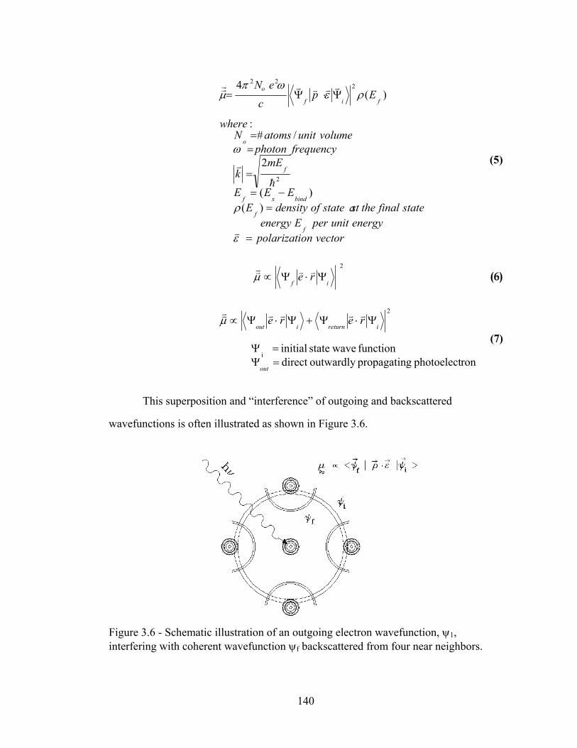
140
vectoronpolarizatienergyunitperEenergy
statefinalthetasstateofdensityEEEE
mEk
frequencyphotonvolumeunitatomsN
where
Epc
eN
f
f
bindxf
f
o
fif
o
=
=−=
=
==
Ψ⋅Ψ=
ε
ρ
ω
ρεωπ
µ
v
h
v
vvvvrr
)( )(
2
/#
:
)(4
2
222
(5)
2
ifre Ψ⋅Ψ∝ vvvvµ
(6)
ronphotoelect gpropagatinoutwardly direct function wavestate initial
i
2
=Ψ=Ψ
Ψ⋅Ψ+Ψ⋅Ψ∝
out
ireturnioutrere vvvvvvµ
(7)
This superposition and “interference” of outgoing and backscattered
wavefunctions is often illustrated as shown in Figure 3.6.
Figure 3.6 - Schematic illustration of an outgoing electron wavefunction, ψ1, interfering with coherent wavefunction ψf backscattered from four near neighbors.

141
potential. scattering atom goriginatin the to returnby influenced-reelectron redbackscatte todueshift phase
wellpotentialr backscatteat shift phase
function ringbackscatte ),(
atoms ringbackscatte and goriginatin between R distance of travel todueshift phase the
atom goriginatin theof wellpotential thedepartingn avefunctioelectron w associatedshift phase the
:where
),(
'1
'1
'1
'1
outback
==
=
=
=
⋅⋅⋅⋅Ψ=Ψ
δ
δ
δ
δδδ
π
π
i
i
ikR
ikR
i
iiikRikR
i
ee
kRekf
Re
e
eekR
ekfR
ee
f
f
(8)
by combining terms in the exponentials we simplify as:
shift phase total the)( :define and
),(
),(
2
))](2([
2
)]22([ '1
≡Ψ
⋅⋅Ψ=
⋅⋅Ψ=
Ψ+
++
k
kRkfe
out
kRkfe
out
j
kkRi
kRi
j
f
π
πδδ
(9)
The absorption can thus be decomposed into terms related to phase shifts
associated with the originating and scattering atoms as well as scattering amplitude
factors. Since, for practical purposes, one is not usually interested in calculation of the
absolute absorption properties of an atomic species, but rather in the information on
nearest neighbor distance and coordination in atomic systems, it is common to
deconvolute the “free atom” portion of the absorption process from the “near
neighbors interference” portion by defining:

142
function EXAFS the)( :
)](1)[(
≡∆
=
−=
o
o
Ewhere
EE
µµχ
χµµ
(10)
All that remains is to formalize the discussion above into quantifiable and calculable
form, sum contributions from all atoms at distance R j and determine an analysis
strategy.
3.2.3 Assumptions and corrections to the basic EXAFS physics
There are inherent and implicit assumptions in such a treatment. First, it is
assumed that the initial state wavefunction, Ψi dimensionality is << than the distance
between absorber and scatterer, R in order to invoke plane wave scattering factors,
|f(k,θ)| (i.e. r << R or kRj << 1). State of the art analysis techniques are currently
advanced to the point of using “curved wave” analysis formalisms. Secondly, for
EXAFS analysis used in this analysis, it is assumed that the outgoing photoelectron
has kinetic energy > 50 eV. This allows the backscattering factor, |f(k,θ)| to be
dominated by terms arising from core potential scattering. This simplifies calculation
of the backscattering amplitude indicated as |f(k,π)| above. Third, it is assumed that
the central atom excited state lifetime (~ 10-15 sec) is greater than the propagation time
for the forward and backscattered wavefronts making the waves self coherent. Finally,
partial wave scattering theory is invoked to allow symmetry arguments between the
outgoing wave scattering and phase shift and the returning wave scattering and phase
shifts eiδ' in the muffin-tin atomic potential region.
Three other correction factors, typical of X-ray, electron and particle
techniques are added. First, to compensate for static thermal disorder (in the harmonic
approximation) a Debye-Waller-like factor is provided. The outgoing photoelectrons
are modified by an inelastic scattering factor to introduce an electron mean free path

143
coherence correction. Finally, understanding that our photon excitation source comes
from the bending magnet of a synchrotron, we understand that the X-rays are highly
polarized. This polarization causes directed photoemission that goes as cos2 of the
angle between the polarization vector of the exciting X-ray photon and the directed
distance r j to the scattering atom.
Inserting all factors outlined above brings us to the “EXAFS Function”,
equation 11 (next page).
3.2.4 SEXAFS Analysis Procedures
The SEXAFS signal must be extracted from the raw x-ray fluorescence
absorption spectrum, Figure 3.7a, through a series of steps, as detailed below. The raw
signal is adjusted by first subtracting out the pre-edge background slope by fitting a
Victoreen function of the form Aλ2 + Bλ4 then defining the absorption edge, the first
derivative inflection point at the edge jump, as the zero point of the energy scale
(Figure 3.7b). Experimental fluorescence spectra were normalized to incident number
of photons during data collection. During analysis they were re-normalized such that a
point 52 eV above the edge at the position of the spline backgound fit was set to a
relative intensity of 1 per suggestions of Sayers and Bunker140.

144
The EXAFS Function:
[ ]
path free mean electron = factor g scatterininelastic = e
disorder staticor fluxuation thermal rms mean = ion)approximat (harmonic factor like-Waller-Debye = e
atom) central excited-photo denotes (prime atom central at shiftphase = )k( atom j from shiftphase ringbackscatte = )k(
)k(2+)k( = shiftphase = )k( term ceinterferen ion wavefunctelectron = )k(+kr2
atomj at )=( amplitude scattering-back electron = f
Emk
rdistance at scattersof Number = N
hellsination sver coord a sum o=
r distance cinteratomi the and vector onpolarizatiray -x between =
atom adsorbing the from R samethe at Zequal of atoms over suma =
absorption atom free = absorption aldifferenti =
modulation EXAFS the = = )k(
WHERE
j
)k(
r2-
j
k 2-
1
thj
1jj
jj
thj
jj
jshell
ijij
ii
0
0
j
j2
j22
j
λ
σ
δφ
δφψψ
πθ
ω
α
µµ
µµχ
λ
σ
r
r
r
r
r
rrr
r
h
hr
r
r
′
′
−=
∠
∆
∆
∑
∑
sin
)(2
,
:
2
20
[ ] e e )k(+kr2 ),k(f rk
N3=)k( )k(r-2
k2-jjj2
j
jij
2
jshellij
j2j
2j r
rrr
rλ
σψπαχ sincos- ∑∑ (11)

145
Next, the oscillatory part of the spectrum due to photoelectrons with energies
greater than 50 eV is stripped from the data set. The data is transformed into
wavenumber, k space as k= 2m(E-Ebind)/ 2 . The non-oscillatory background
component of the spectrum due to an equivalent “free atom” absorption effect is
removed by fitting a five-knot cubic spline function as shown in Figure 3.7c. The
resulting χ(k) function, Figure 3.7d is kn weighted (where n=3 for periods 1,2,3,4, n=2
for period 5 and n=1 for periods 6+) to compensate for k dependences in the
scattering potentials as a function of Z. Normally, upon transformation from energy to
k space, elements such as Ag, from the fourth period are commonly k2 weighted to
symmetrize the peaks in the Fourier transform by selective weighting the higher k
contributions. Aebi, et.al.141 has argued that k2 weighting contributes unnecessarily to
a loss of low-k information detrimental to low-Z backscatters like Si whose
backscattering amplitude peaks at near 1 A-1 and suggests k1 weighting. Following
this advice, all experimental χ(k) data is k1 weighted, at variance with pre-1995
common practice, Figure 3.7e.
The resulting k ·χ(k) function is Fourier transformed producing a first
approximation to the radial distribution function as shown in Figure 3.7f. In this
example an Ag nearest-neighbor distance of 2.575 Å is found, within 11% of the
textbook value of 2.889 Å. To further refine this radial distribution function, phase
shifts must be adjusted, normally by comparison with reference standards containing
the same absorber-nearest neighbor atom pairs but with known bond lengths. As
shown in Figure 3.7f, the first approximation radial distribution function is fit with an
Hanning window to select individual atom pair contributions to the spectrum.
This filtered spectrum is then back-Fourier transformed, shown in Figure 3.7g
with the additional advantage that the multivariate problem of Equation 11 is now
reduced to roughly seven degrees of freedom. The resulting back transformed

146
wavefunction, has an amplitude envelope, A(k ) containing information on the number
of nearest neighbors, and an oscillatory component, sin ϕ(k ), containing the
information on the scattering pairs and inter-atomic distances.
The sin ϕ(k ) component, which from Equation 11 is composed of two terms,
[ ])k(+kr2 jj
rψsin , is fit with appropriate amplitude and phase parameters. Using the
interatomic distances of the known standard and assuming that chemical
transferability is not dependant on binding energies, the unknown backscattering phase
shift parameter, )k(j
rψ is determined to be back transferred to the unknown spectrum
as shown in Figure 3.7h.
The resulting filtered and phase adjusted spectra is again Fourier transformed.
The real and imaginary forward transformed components are combined, Figure 3.7i,
creating a |FT| magnitude envelope with the closest determination of the actual radial
distribution function for that pair’s atomic distance and nearest neighbor information.
In the case of our example using an ideal Ag standard material and excellent
experimental counting statistics, we find an Ag-Ag bond length of 2.878 ± 0.010 Å; a
result within 1% of handbook values of 2.889 Å.
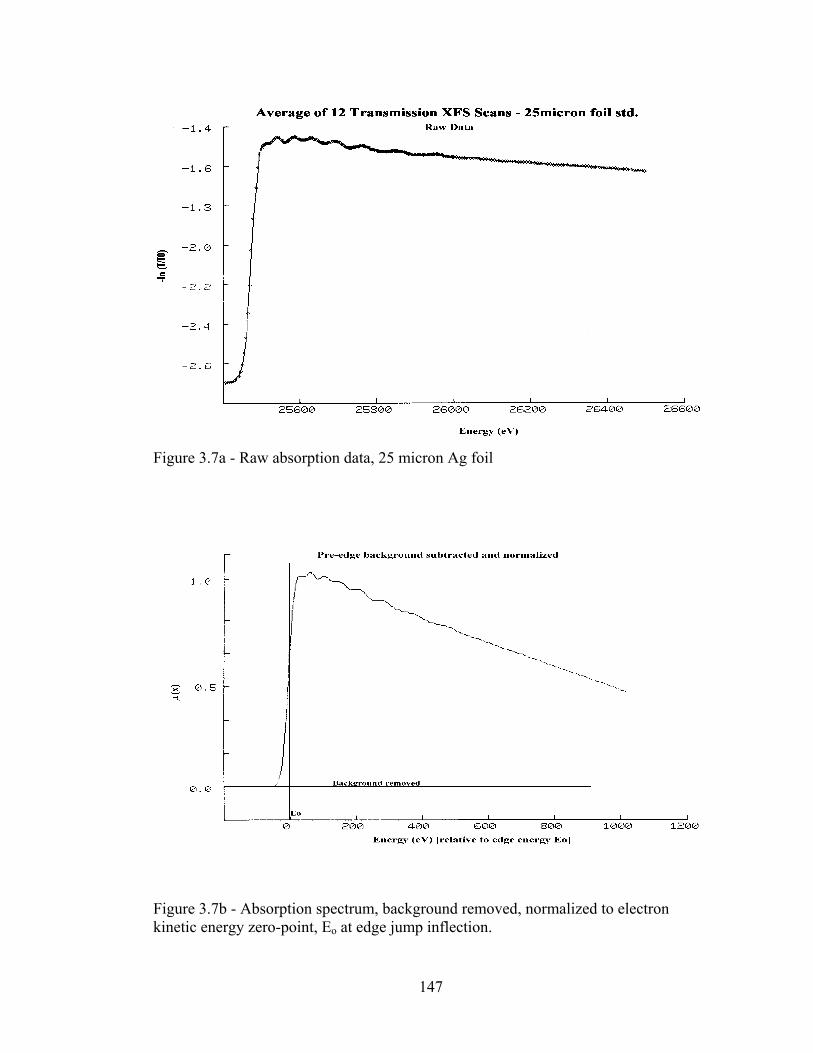
147
Figure 3.7a - Raw absorption data, 25 micron Ag foil
Figure 3.7b - Absorption spectrum, background removed, normalized to electron kinetic energy zero-point, Eo at edge jump inflection.

148
Figure 3.7c - Spline fit to remove "free atom" contribution to the XFS oscillations
Figure 3.7d - The "Chi Function", χ(k )
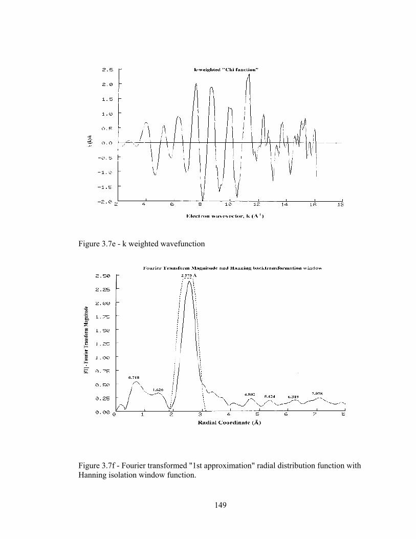
149
Figure 3.7e - k weighted wavefunction
Figure 3.7f - Fourier transformed "1st approximation" radial distribution function with Hanning isolation window function.
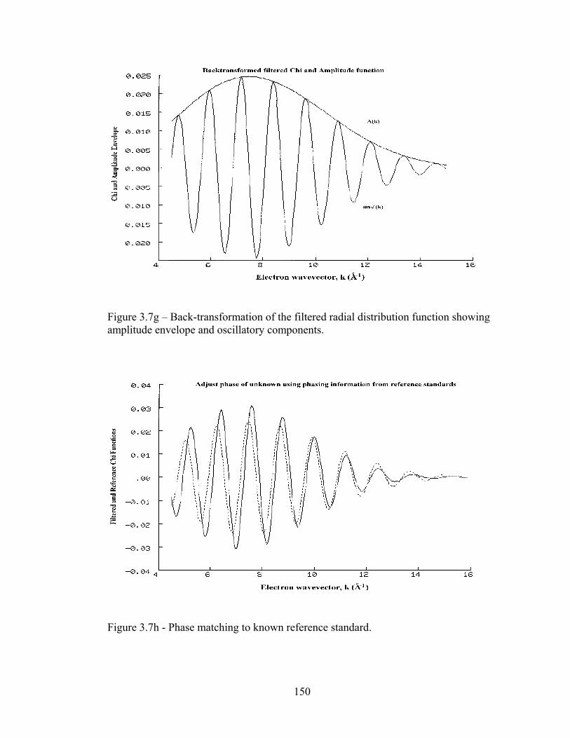
150
Figure 3.7g – Back-transformation of the filtered radial distribution function showing amplitude envelope and oscillatory components.
Figure 3.7h - Phase matching to known reference standard.

151
Figure 3.7i - Back-transformation of filtered and phase adjusted wavefunction showing real (solid) and imaginary (dashed) components of the Fourier transformation.
Figure 3.7j - Final single-pair radial distribution function solved, dN-N = 2.878 Å.

152
3.3 Quantitative Auger Electron Spectroscopy (AES)
In most surface studies, it is desirable to find the quantity of a surface element
or surface contamination using Auger Electron Spectroscopy (AES). In the case of
Ag/Si(111), critical differences between 2/3 and 1 ML coverages influences model
choices. Of equal importance is the determination of surface cleanliness levels. As
we shall discuss later, carbon contamination plays a crucial role in surface structure
formation so accurate quantitation is imperative. Many studies cite the misinformed
notion that they obtained a clear Si(111)-(7x7) pattern with LEED therefore the
surface must be clean. Numerous observations during this series of experiments have
shown that clear Si-(7x7) LEED patterns can be obtained with 30% C contamination
levels where C contamination levels of under 3% drastically influence surface
structure and suppress Ag-(3x1) formation.
Quantification of raw deposition amounts often rely on reference to an external
quartz crystal oscillator thickness monitor142. In-situ surface adsorbate measurements
require AES quantitation. It is most common to find reference in the literature to
coverages determined by the method of standards, by the method of Elemental
Sensitivity Factors143, 144 or by a thin layer simplification of for the Ag/Si p-p ratio145.
Even using the most complete first principles calculations for this study, AES
coverage determinations for submonolayer deposits were estimated high by up to a
factor of 10x compared with rigorous RBS measurements.
In the vast majority of studies including this one, AES spectra are measured as
differential, dN(E)/dE vs. Auger electron energy as shown in Figure 3.8. The peak-to-
peak height for the characteristic substrate and overlayer elements are used to
calculate relative abundances.

153
Figure 3.8 - CMA measured Auger electron spectra for Si, Ag and C. (After Davis144) Ag MNN peaks identified by Housley, Heckingbottom and Todd146 and Si LVV peaks in LeLay notation where V2 represents a lower 3s-like final state and V4 indicates an 3p-like final state.

154
3.3.1 Quartz oscillator crystal measurements
Direct measurement of Ag deposition rate is most easily accomplished by
allowing an AT-cut quartz crystal slice to intercept the incoming Ag stream at the
position of the substrate. The increase in mass of this crystal, vibrating in the MHz
frequency range, as Ag adsorbs causes an easily measurable shift of its resonance
frequency. From this frequency shift, the mass increase and therefore deposit
thickness can be calculated in a straightforward manner. An excellent primer on the
quartz crystal technique can be found in Ashworth and Shacklette142 and frequency
shift to mass calculations can be found in Ridgway and Haneman147. Pre-packaged
commercial units can be purchased that calculate deposition amounts and rates in real-
time. One must remember that unless the quartz monitor head is in the same position
as the sample, there is a 1/r2 distance effect that many do not take into account.
3.3.2 AES standards and sensitivity factor methods
To zeroth-order, if one measures the AES p-p (peak-to-peak) height of a pure
standard then a dilute surface deposit of the same element with the same instrument
under the same experimental conditions, the concentration of the dilute element is
directly proportional to the ratio of the AES p-p height of the standard. To avoid the
experimental complications of mounting and preparing numerous pure standards,
using one standard with a high sensitivity factor to scale your experimental conditions
has become common. That standard element happens to be silver and the relative
sensitivity for Auger emission of all elements against that standard under various
excitation conditions is well known. Experimental determination of a dilute
concentration of any element measured relative to a Ag standard can be simply
calculated using scaling factors for that element vs. silver although accuracy is
necessarily sacrificed over the method of pure standards.

155
If a standard is not included in AES measurements, good estimates of relative
concentration can be made by measuring the major and minor component AES
response, adsorbate and substrate in our case, and scaling their p-p heights using the
same sensitivity factors. (See Davis144) Again, accuracy suffers over the Ag standard
method.
In all cases, these experimental (quartz oscillator) and computational
(standards and sensitivity factor) methods work well for high concentrations and thick
adsorbate layers. It will be shown in the experimental section of Chapter 5 that each
of the techniques becomes less and less reliable when applied to vanishingly small
quantities, tenths of monolayers, on surfaces as studied in this dissertation. Even thin
film approximations145 and first principles calculations have difficulties with these
extremely dilute systems.
3.3.3 AES first principles calculations
The experimentally detected surface Auger signal, I αXYZ arising from some
distribution of N atoms is a function of the incident probe flux J, an interaction cross-
section, σ, between the probe beam and the surface atoms, the Auger yield per
interaction, ω, and a detector efficiency factor, f as:
ωσα JNf=I XYZ (12)
These factors are customary expanded to the form:
dter)E,E((t)ndEd
41=I
t-*Rpx0
EE XYZ
p
xXYZ λαααα αγσπ ∫∫Ω∫ ∞
(13)
where the first integral is over the detector solid angle, the second integral is over the
energy range between Auger electron energy and the primary electron beam energy
and the third integral is over penetration depth into the probed solid.

156
Three simplifying assumptions are usually made at this time. First, the sample
composition is assumed to be homogeneous over the probed volume. This allows the
nα(t), atomic distribution, and γα, Auger yield to be pulled from the integrals.
Secondly, since the Auger electrons come from such a thin surface layer, the probe
current, Ip, is assumed constant, the probe energy, Ep, is assumed constant and thus the
backscattering coefficient, R*, can be pulled out of the energy and thickness integrals.
Finally, since the majority of the Auger excitations are produced by the direct probe
beam or by secondary electrons, both with energy near that of the probe beam, Ep, the
ionization cross-sections can be approximated by one at energy Ep for core-hole
excitations of energy Ex. The remaining integral over the detector solid angle, probe
angle and sample roughness are condensed into a transmission function, T. These
detector dependant factors are different for an electrostatic 127° sector analyzer148, a
retarding field analyzer (RFA)149, an angular resolved secondary electron spectrometer
(ARSES) or a cylindrical mirror analyzer (CMA)150 instrument. Finally, the
roughness factor, r*, and is considered a constant for a given experimental set-up.
With these simplifying but reasonable assumptions, Palmberg151 showed that a
first principles calculation of Auger peak intensity involves a function of the form:

157
Equation 12 is the usual starting point for Auger quantitation calculations.
Calculating these components is fraught with uncertainty and experimental variability.
For the particular example of this research, we are primarily concerned with
Ag M4,5N4,5N4,5 and Si L2,3VV Auger electrons as indicators of surface coverage. The
ionization cross-sections, σα(x, Ep) can be estimated from Worthington and Tomlin152
calculations for K and L shells. A better approximation with no free parameters and
with some hope for M and N shell applicability is the semi-classically derived
Gryzinski153 formulation. The Auger Yield term, γαxyz, is well approximated by
Siegbahn’s154 polynomial for K electrons. Formalism for L, M and higher shell Auger
yields are similar but less accurately predicted.
Factor Roughness Sample
factorsdetection andion transmissalinstrumentboth combining Functionon Transmissi RFA)or (CMA er Spectromet
(eV)Energy Electron redBackscatte(eV)Energy BeamPrimary
Factors ringBackscatte
β and α elements of nspermutatiofor depth escapeAuger
Transition XYZ α,Element Yield,Auger
(eV)Energy BeamPrimary number quantum Orbital
αelement seciton,-cross Ionization
αelement atoms, emittingAuger ofnumber
(mA)Current BeamPrimary
Transition XYZα,Element Intensity,Auger
,
= r
= T
= E = E
= )E ,E(R
=
=
= E = x
= )E(x,
= n
= I
= I
:Where
r)]TE,E(R+[1)E(xnI = I
*R
x
p
xp*
p
p
p
*Rxp
*pp
xyz
xyz
XYZXYZ
β
β
α
βα
α
α
α
α
αβααααα
λ
γ
σ
λγσ
(14)
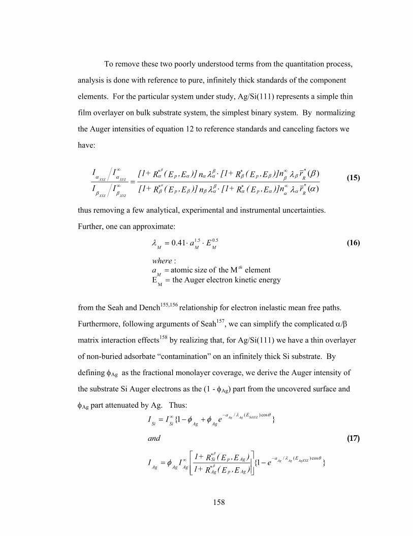
158
energy kineticelectron Auger theEelement M theof size atomic
:
41.0
M
5.05.1
==
⋅⋅=
thM
MMM
awhere
Eaλ
To remove these two poorly understood terms from the quantitation process,
analysis is done with reference to pure, infinitely thick standards of the component
elements. For the particular system under study, Ag/Si(111) represents a simple thin
film overlayer on bulk substrate system, the simplest binary system. By normalizing
the Auger intensities of equation 12 to reference standards and canceling factors we
have:
(15)
thus removing a few analytical, experimental and instrumental uncertainties.
Further, one can approximate:
(16)
from the Seah and Dench155,156 relationship for electron inelastic mean free paths.
Furthermore, following arguments of Seah157, we can simplify the complicated α/β
matrix interaction effects158 by realizing that, for Ag/Si(111) we have a thin overlayer
of non-buried adsorbate “contamination” on an infinitely thick Si substrate. By
defining φAg as the fractional monolayer coverage, we derive the Auger intensity of
the substrate Si Auger electrons as the (1 - φAg) part from the uncovered surface and
φAg part attenuated by Ag. Thus:
1
1
cos)(/
cos)(/
θλ
θλ
β
β
φ
φφ
AgXYZAgAg
SiXYZAgAg
Ea
Agp*Ag
Agp*Si
AgAgAg
Ea
AgAgSiSi
e)E,E(R+1)E,E(R+1
II
and
eII
−∞
−∞
−
=
+−=
(17)
)(
)(
αλλ
βλλ
ααααβαβββ
βββββαααα
ββ
ααα
β
*Rp
*p
*
*Rp
*p
*
r)]nE,E(R+[1n)]E,E(R+[1
r)]nE,E(R+[1n)]E,E(R+[1
II
II
XYZXYZ
XYZXYZ
∞
∞
∞
∞
⋅
⋅=
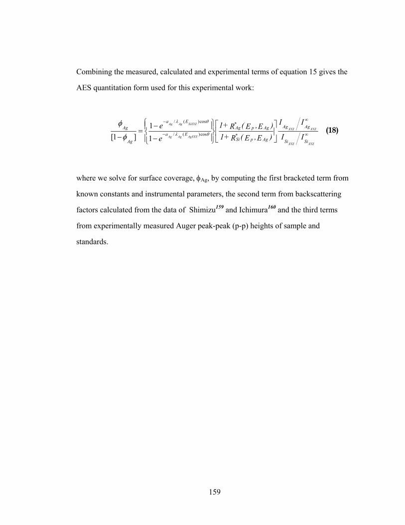
159
Combining the measured, calculated and experimental terms of equation 15 gives the
AES quantitation form used for this experimental work:
(18)
where we solve for surface coverage, φAg, by computing the first bracketed term from
known constants and instrumental parameters, the second term from backscattering
factors calculated from the data of Shimizu159 and Ichimura160 and the third terms
from experimentally measured Auger peak-peak (p-p) heights of sample and
standards.
∞
∞
−
−
−
−=
−XYZXYZ
XYZXYZ
AgXYZAgAg
SiXYZAgAg
SiSi
AgAg
Agp*Si
Agp*Ag
Ea
Ea
Ag
Ag
II
II
)E,E(R+1)E,E(R+1
ee
θλ
θλ
φ
φcos)(/
cos)(/
11
]1[

160
3.4 Rutherford Backscattering Spectroscopy (RBS)
As in the more general field of Ion Scattering Spectroscopy (ISS), the sub-field
of Rutherford Backscattering Spectrometry involves “hard sphere” collisions between
incident particles and subject materials as schematically illustrated in Figure 3.9. For
introductory material, the reader is directed to the texts by Chu, Nicolet and Mayer161
or Feldman and Mayer132 and the review article by Nicolet, et. al. 162
Figure 3.9 - Schematic of RBS analysis of Ag/Si(111). A 2.7 MeV He++ ion with initial kinetic energy and momentum recoils elastically after collision with a surface atom.
The scattered or channeled probe particles are analyzed for scattering angle
and residual kinetic energy. Calculations of the energy transfer kinematics are well
understood resulting in compositional analysis of the target substance. Starting with
the assumption of non-relativistic velocities and elastic scattering we proceed using

161
classical mechanics and write the equations for the conservation of energy, E, and
momentum, p :
(20)
Combining the two p conservation equations and substituting into the E equation we
define K, the kinematic factor as:
(21)
For surface scattering, the final energy of the scattered He++ ion equals:
o
KEE =1
(22)
independent of the initial kinetic energy of the He++ ion and only modified by the
scattering angle and mass ratio of the elements.
For areal quantitation we also need the collision cross-section between the
incident Mo particle and the surface target, M2. Using classical electrostatics,
Rutherford163 determined that the differential cross-section can be represented as:
(23)
Entering the appropriate proportionality factors for units of Å2/steradian, making the
reasonable assumption that the He++ atom is much less massive than the target atoms,
2
222
2
2
2
:1
)(sin1)cos(
MM
x
wherex
xxEE
vv
K
o
oo
=
+−+
==
=
ϑϑ
)sin()sin(0
onconservati p )cos()cos(
onconservati E 21
21
21
221
221
222
21
2
ϕϑ
ϕϑ
vMvM
vMvMvM
vMvMvM
o
ooo
ooo
+=
+=
+=
v
( ) ( )
−
−+∝
Ω )(sin1)(sin
)(sin1)cos(4224
222
2
2
2
ϑϑ
ϑϑσ
x
xE
ZZ
dd
o
o

162
x< ½ and performing appropriate trigonometric manipulation, we derive a form for the
differential scattering cross section for Coulomb scattering/unit solid angle of:
(24)
Now repeating the logic used in Auger quantitation, Equation 10 we have:
(25)
an equation that gives quantitative measurement of atom specific surface density with
no free parameters. Detected signal, IRBS is subject to counting statistics. Detector
solid angle and take-off angle can be precisely determined, incident beam current can
be measured as a sample current with precision pico-ammeters, scattering cross
section has no free parameters and backscattering yield, as a primary process, is unity.
Fits using equations 19 and 20 determine atom specificity. Fits using equations 22
and 23 with calibrated detectors and electronics determine atomic quantities for those
surface atoms.
In the specific instrument used for this work, 2.7 MeV 4He++ ions were
extracted from the Cornell MSC Tandetron after separation from other ions using a
15° sector magnet and collimated with standard slit systems. These ions were directed
at Ag/Si and reference standard materials. The 7° tilt indicated in Figure 3.7 is
necessary to avoid ion channeling effects. Ions backscattered at 170° were analyzed to
determine quantitatively, the areal density of Ag atoms (high Z) on Si (low Z).
yield ringbackscatte22)equation (fromsection -cross scattering
densitycurrent beamincident density) (areal atoms scattering ofnumber
) angle, solid(detector collection fractional rate signal RBS measured
:
====
Ω==
ωσ
ωσ
JN
dfIwhere
JNf=I
RBS
RBS
( )
−=
Ω )2/(sin)2/(sin2196.12
4
22
2
2
2
ϑϑσ x
EZZ
dd
o
o

163
Analysis was done using the computer program RUMP and fitting algorithms
developed by Doolittle164, 165.
RBS is unique in its ability to detect at the ~1010 atoms/cm2 for heavy elements
on light element substrates. This sensitivity level far greater than needed to
distinguish a single Ag/Si(111) monolayer coverage of 7.83 x 10¹⁴ atoms/cm2 and is
unique in providing absolute coverage quantitation.

164
3.5 References -Chapter Three 31 M. von Laue, Ergb. Exakten Naturwiss. 10, 133 (1931). 32 M. von Laue, Ann. Physik (Leipzig) 23, 705 (1935). 33 M. von Laue, Röntgenstrahlinterferenzen (Akademische Verlagsgesellschaft, Frankfurt/Main, 1960). 34 M. von Laue, Acta Crystallogr. 2, 106 (1966). 35 B.W. Batterman and H. Cole, Rev. Modern Phys. 36, 681 (1964). 36 G. Borrmann, Z. Physik. 42, 157 (1941). 37 B.W. Batterman, Appl. Phys. Let. 1, 68 (1962). 38 B.W. Batterman, Phys. Rev. 133, A759 (1964). 39 B.W. Batterman, Phys. Rev. Let. 22, 703 (1969). 40 A.M. Afanas'ev, V.N. Peregudov, Sov. Phys. Dokl. 33, 607 (1988). 41 G.C. La Rocca, J. Zegenhagen, Phys. Rev. B 44, 13666 (1991). 42 A.M. Afanasev, R.M. Imamov, R.K. Mukhamedzhanov, L.C. Qui, Phys. Status Solidi 92, 355 (1985). 43 L.A. Smirnov, T.D. Sotnikova, Y.I. Kogan, Opt. & Spectrosc. 58, 239 (1985). 44 J.A. Golovchenko, J.R. Patel, DARPA Conference, (1984). 45 K. Akimoto, S. Kikuta, J. Crystallogr. Soc. Jpn. 26, 228 (1984). 46 M.V. Koval'chuk, E.K. Mukhamedzhanov, Phys. Status Solidi A 81, 427 (1984). 47 J. Auleytner, J. Majewski, Surf.Sci. 231, 227 (1990). 48 M. Kuriyama, G.G. Cohen, Z. Naturforsch. A 37, 465 (1982). 49 J. Zegenhagen, Surf. Sci. Reports 18, 199 (1993).

165
50 S.I. Zheludeva, M.V. Koval'chuk, N.N. Novikova, A.N. Sosphenov, N.E. Malysheva, N.N. Salashchenko, A.D. Akhsakhalyan, Thin Solid Films 232, 252 (1993). 51 M.V. Koval'chuk, V.G. Kohn, Sov. Phys. Usp. 29, 426 (1986). 52 A. Authier, Acta.Crys. A 42, 414 (1986). 53 M.J. Bedzyk, Nucl. Inst. M (preprint) (1987). 54 S.K. Andersen, J.A. Golovchenko, G. Mair, Phys. Rev. Let. 37, 1141 (1976). 55 M.J. Bedzyk, G. Materlik, M.V. Kovalchuk, Phys. Rev. B 30, 2453 (1984). 56 M. Kerkar, D. Fisher, D.P. Woodruff, B. Cowie, Surf. Sci. 271, 45 (1992). 57 S.M. Durbin, J. Appl. Phys. 64, 2312 (1988). 58 D.P. Woodruff, D.L. Seymour, C.F. McConville, C.E. Riley and M.D. Crapper, Phys. Rev. Let. 58, 1460 (1987). 59 D.P. Woodruff, D.L. Seymour, C.F. McConville, C.E. Riley and M.D. Crapper, Surf. Sci. 195, 237 (1988). 60 J. Zegenhagen, G. Materlik, Synch. Rad. News 6, 19 (1993). 61 G. Materlik, J. Zegenhagen, W. Uelhoff, Phys. Rev. B 32, 5502 (1985). 62 A.M. Afanasev, R.M. Imamov, E.Kh. Mukhamedzhanov, A.A. Bzheumikhov, Phys. Stat. Sol. A 116, 197 (1989). 63 M.J. Bedzyk, G. Materlik, DESY Internal Report, SR 85-07 (1985). 64 S. Annaka, T. Takahashi, S. Kikuta, Jpn. Jour. Appl. Phys. 23, 1637 (1984). 65 M.J. Bedzyk, G. Materlik, Phys. Rev. B 32, 6456 (1985). 66 Y. Saitoh, H. Hashizume, K. Tsutsui, Jpn. Jour. Appl. Phys. 27, 1386 (1988). 67 S. Maeyama, M. Sugiyama, M. Oshima, H. Oigawa and Y. Nannichi, Appl. Surf. Sci. 60, 513 (1992).

166
68 T. Kendelewicz, J.C. Woicik, K.E. Miyano, P.L. Cowan and B.A. Karlin, J. Vac. Sci. Technol. B 9, 2290 (1991). 69 M.V. Kovalchuk, E.Kh. Mukhamedzhanov, Sov. Phys. Sol. State 25, 2033 (1983). 70 N. Greiser, G. Materlik, Z. Phys. B 66, 83 (1987). 71 S.M. Durbin, L.E. Berman, M.J. Bedzyk, B.W. Batterman, J.M. Blakely, J. Vac. Sci. Technol. A 4, 1329 (1986). 72 M.J. Bedzyk, S.M. Durbin, L.E. Berman, unpublished. 73 P.L. Cowan, S. Brennan, T. Jach, M.J. Bedzyk, G. Materlik, Phys. Rev. Let. 57, 2399 (1986). 74 M.J. Bedzyk, G. Materlik, Phys. Rev. B 31, 4110 (1985). 75 M. Bedzyk, G. Materlik, Surf. Sci. 152, 10 (1985). 76 M.J. Bedzyk, Q. Shen, M.E. Keeffe, G. Navrotski, L.E. Berman, Surf. Sci. 220, 419 (1989). 77 P.L. Cowan, Phys. Rev. B 32, 5437 (1985). 78 J.A. Golovchenko, B.W. Batterman, W.L. Brown, Phys. Rev. B. 10, 4239 (1974). 79 B.W. Batterman, Appl. Phys. Let. 1, 68 (1962). 80 T. Ohta, H. Sekiyama, Y. Kitajima, H. Kuroda, T. Takahashi, S. Kikuta, Jpn. J. Appl. Phys. Let. 24, 475 (1985). 81 M. Funabashi, T. Yokoyama, Y. Takata T. Ohta, Y. Kitajima, H. Kuroda, Surf. Sci. 242, 59 (1991). 82 E. Fontes, J.R. Patel, F. Comin, Preprint, (1992). 83 J. Zegenhagen, J.R. Patell. B.M. Kincaik, J.A. Golovchenko, J.B. Mock, et.al. Appl. Phys. Let. 53, 252 (1988). 84 Y. Qian, M.J. Bedzyk, J. Vac. Sci. Technol.A 13, 1613 (1995). 85 G. Materlik, J. Zegenhagen, Phys. Let. A 104, 47 (1984).

167
86 N. Hertel, G. Materlik, J. Zegenhagen, Z. Phys. B 58, 199 (1985). 87 P.L. Cowan, J.A. Golovchenko, M.F. Robbins, Phys. Rev. Let. 44, 1680 (1980). 88 B.N. Dev, T. Thundat, W.M. Gibson, J. Vac. Sci. Technol. A 3, 946 (1985). 89 S.M. Durbin, L.E. Berman, B.W. Batterman, J.M. Blakely, Phys. Rev. Let. 56, 236 (1986). 90 A.M. Afanas'ev, E.A. Manykin, E.F. Lobanovich, M.V. Koval'chuk, R.M. Imamov, Sov. Phys. Sol. State 24, 1473 (1982). 91 E. Vlieg, E. Fontes and J.R. Patel, Phys. Rev. B 43, 7185 (1991). 92 E. Vlieg, E. Fontes and J.R. Patel, in The Structure of Surfaces III (Tong, van Hove and Takayanagi, eds.) Springer-Verlag, p595-599 (1991). 93 L.E. Berman, B.W. Batterman, J.M. Blakely, Phys. Rev. B 38, 5397 (1988). 94 L.E. Berman, B.W. Batterman, J.M. Blakely, Cornell University MSC Report #6418 (1988). 95 S.M. Durbin, L.E. Berman., B.W. Batterman, J.M. Blakely, Phys. Rev. B 33, 4402 (1986). 96 S.M.Durbin, L.E.Berman, B.W.Batterman, J.M.Blakely, J. Vac. Sci. Technol. A 3, 973 (1985). 97 P. Funke, G. Materlik, Surf. Sci. 188, 378 (1987). 98 B.N. Dev, V. Aristov, N. Hertel, T. Thundat, W.M. Gibson, Surf. Sci. 163, 457 (1985). 99 J.A. Golovchenko, J.R. Patell., D.R. Kaplan, P.L. Cowan, M.J. Bedzyk, Phys. Rev. Let. 49, 560 (1982). 100 B.N. Dev, V. Aristov, N. Hertel, T. Thundat, W.M. Gibson, J. Vac. Sci. Technol. A 3, 975 (1985). 101 G. Materlik, A. Frahm, M.J. Bedzyk, Phys. Rev. Let. 52, 441 (1984). 102 P. Funke, G. Materlik, Solid State Comm. 54, 921 (1985).

168
103 M.J. Bedzyk, Ph.D Thesis, State University of New York, Albany(1982). 104 M.J. Bedzyk, W.M. Gibson, J.A. Golovchenko, J. Vac. Sci. Technol. 20, 634 (1982). 105 S. Lagomarsino, F. Scarinci, P. Castrucci, C. Giannili, E. Fontes and J.R. Patel, Appl. Surf. Sci. 56, 402 (1992). 106 J. Zegenhagen, J.R. Patel, P. Freeland, D.M. Chen, and J.A. Golovchenko, Phys. Rev. B 39, 1298 (1989). 107 J. Zegenhagen, M.S. Hybertsen, P.E. Freeland and J.R. Patel, Phys. Rev. B 38, 7885 (1988). 108 J.R. Patel, P.E. Freeland, M.S. Hybertsen, D.C. Jacobson and J.A. Golovchenko, Phys. Rev. Let. 59, 2180 (1987). 109 J.R. Patel, J.A. Golovchenko, J.C. Bean, R.J. Morris, Phys. Rev. B. 31, 6884 (1985). 110 J. Zegenhagen, J.R. Patel, E. Fontes, Appl. Surf. Sci. 60, 505 (1992). 111 B.N. Dev, G. Materlik, F. Grey, R.L. Johnson, M. Clausintzer, Phys. Rev. Let. 57, 3058 (1986). 112 J.R. Patel, P.E. Freeland, J.A. Golovchenko, A.R. Kortan, D.J. Chadi, G-X Qian, Phys. Rev. Let. 57, 3077 (1986). 113 J.C. Woicik, T. Kendelewicz, A. Herrera-Gomez, A.B. Andrews, B.S. Kim, et.al. J. Vac. Sci. Technol. A 11, 2359 (1993). 114 Th. Gog, G.C. Follis, S.M. Durbin, Applied Surf. Sci. 81, 485 (1994). 115 J. Zegenhagen, K.G. Huang, W.M. Gibson, B.D. Hunt, L.J. Schowalter, Phys. Rev. B 39, 10254 (1989). 116 K. Akimoto, T. Ishikawa, T. Takahashi, S. Kikuta, Jpn. Jour. Appl. Phys. 24, 1425 (1985). 117 K. Akimoto, T. Ishikawa, T. Takahashi, S. Kikuta, Jpn. Jour. Appl. Phys.(Let.) 22, 798 (1983).

169
118 K. Akimoto, R. Ishikawa, T. Takahashi, S. Kikuta, Nucl. Inst. Meth. A 246, 755 (1986). 119 E. Vlieg, A. Fischer, J.F. Van Der Veen, B.N. Dev, G. Materlik, Surf. Sci. 178, 36 (1986). 120 K.G. Huang, W.M. Gibson, J. Zegenhagen, Phys. Rev. B 40, 4216 (1989). 121 B.N. Dev, G. Materlik, F. Grey, R.L.J ohnson, Unpublished(?)preprint from author. 122 V. Elaniemi, E.G. Michel, G. Materlik, Surf. Sci. 287, 288 (1993). 123 M.V. Koval'chuk, V.G. Kon, E.F. Lobanovich, Sov. Phys. Solid State 27, 2034 (1985). 124 M. Bedzyk, G. Materlik, M.V. Kovalchuk, DESY Internal Report, 301, (1985). 125 V. Elaniemi, E.G. Michel, G. Materlik, J. Vac. Sci. Technol. A 13, 1583 (1995). 126 M.J. Bedzyk, D. Bilderback, J. White, H.D. Abruna, M.G. Bommarito, Jour. Phys. Chem. 90, 4926 (1986). 127 T.W. Barbee, W.K. Warburton, Mater. Let. 3, 17 (1984). 128 M.J. Bedzyk, G.M. Bommarito, J.S. Schildkraut, Phys. Rev. Let. 62, 1376 (1989). 129 Jin Wang, M.J. Bedzyk, M. Caffrey, Science 258, 775 (1992). 130. R. Kronig, Z. Phys. 70, 317 (1931); Z. Phys. 75, 475 (1932); Z. Phys. 76, 468 (1932). 131. Ertl, Küppers, Low Energy Electrons and Surface Chemistry, VCH, (1985) 267-282. 132. L.C. Feldman and J.W. Mayer, Fundamentals of Surface and Thin Film Analysis, North-Holland (1986).. 133. Zangwill, Physics at Surfaces, Cambridge (1988) 245-256. 134. J. Stöhr, Surface Crystallography by Means of SEXAFS and NEXAFS, in Chemistry and Physics of Solid Surfaces, (R. Vanselow and R. Howe, eds.), Springer Verlag, (1984) 231-255.

170
135.E.A. Stern, Theory of the extended x-ray-absorption fine structure, Phys.Rev.B 10, 3027 (1974). 136. E.A. Stern, D.E. Sayers and F.W. Lytle, Extended x-ray-absorption fine-structure technique. III. Determination of physical parameters, Phys.Rev.B 11, 4836, (1975). 137. F.W. Lytle, D.E. Sayers and E.A. Stern, Extended x-ray-absorption fine-structure technique II. Experimental practice and selected results, Phys.Rev.B 11, 4825 (1975). 138. P.A. Lee, P.H. Citrin, P. Eisenberger and B.M. Kincaid, Extended x-ray absorption fine structure - its strengths and limitations as a structural tool, Reviews of Modern Physics, 53, #4, part 1 (1981) 769-806. 139. D.C. Koningsberger and R. Prins, X-Ray Absorption, Principles, Applications, Techniques of EXAFS, SEXAFS and XANES, John Wiley & Sons, 1988. 140. D.E. Sayers and B.A. Bunker, "Data Analysis", Chapter 6 in Koningsburger, X-Ray Absorption Principles, Applications, Techniques of EXAFS, SEXAFS and XANES, John WIley (1988) p216-217. 141. P.Abei, et.al. Phys. Rev. B 45, 13582, 1992. 142 H.A. Ashworth and L.W. Shacklette, Rev. Sci. Instrum. 49, 1653 (1978) 143 P.W. Palmberg, J. Vac. Sci. Technol. 13, 214 (1976) 144 L.E. Davis, N.C. McDonald, P.W. Palmberg, G.E. Raich and R.E. Weber, Handbook of Auger Electron Spectroscopy, Perkin-Elmer Corporation, Physical Electronics Division, Eden Prairie, Minnesota, 2nd edition (1978). 145 J.P. Bibeian and G.A. Somoraji, Appl. Surf. Sci. 2, 352 (1979). 146 M. Housley, R. Heckingbottom and C.J. Todd, Surf. Sci. 68, 179, (1977). 147 J.W.T. Ridgway and D. Haneman, Surf. Sci. 24, 451-458 (1971). 148 L.A. Harris, J. Appl. Phys. 39, 1419 (1968). 149 N.J. Taylor, Rev. Sci. Instrum. 40, 792 (1969). 150 P.W. Palmberg, G.K. Bohn and J.C. Tracy, Appl. Phys. Let. 15, 254 (1969). 151. P.W. Palmberg, J. Vac. Sci. Technol. 13 (1976) 214.

171
152 Worthington and Tomlin, Proc. Phys. Soc. London A 69, 401 (1956). 153 Gryzinski, Phys. Rev. A 138, 336 (1965). 154 K. Siegbahn, C.N. Nordling, A. Fahlman, R. Nordberg, K. Hamrin, J. Hedman, G. Johansson, T. Bergmark, S.E. Karlsson, I. Lindgren and B. Lindberg, ESCA, Atomic, Molecular and Solid State Structure Studied by Means of Electron Spectroscopy (Almqvist and Wiksells, Uppsala, Sweden, 1967). 155 M.P. Seah and W.A. Dench, Surf. Interface Anal. 1, 2 (1979). 156 M.P. Seah, Surf. Interface Anal. 9, 85 (1986). 157 M.P. Seah, Chapter 5 in Practical Surface Analysis by Auger and X-ray Photoelectron Spectroscopy (D. Briggs and M.P. Seah, eds.)John Wiley and Sons (1983) 158 Th. Wirth, Surf. Interface Anal. 18, 3 (1992). 159 R. Shimizu, Jpn. J. Appl. Phys. 22, 1631 (1983). 160 S. Ichimura and R. Shimizu, Surf. Sci. 112, 386 (1981). 161 W.K. Chu, M.A. Nicolet and J.W. Mayer, Backscattering Spectrometry (Academic Press, N.Y., 1977). 162 M.A. Nicolet, “Backscattering Spectrometry and Related Analytical Techniques”, p581, in Materials Characterization using Ion Beams, (J.P. Thomas and A. Cachard eds.) Plenum Press, N.Y. (1978). 163 E. Rutherford, Phil. Mag. 21 669 (1911). 164 L.R. Doolittle, Nucl. Instrum. Methods B 9, 344 (1985). 165 L.R. Doolittle, Nucl. Instrum. Methods B 15, 227 (1986).

172
CHAPTER FOUR:
EXPERIMENTAL METHODS
4.1 Ultra-high Vacuum System
As mentioned, two of the three experimental variables studied in this
experiment involve control of traditional "surface contaminants". This study required
a contamination free, especially boron and carbon contamination free, ultra-high
vacuum system (UHV). The system, constructed by the author, can be thought of as
two vacuum subsystems, a lower pumping well and an upper twenty inch diameter
spherical analysis chamber. The vacuum unit, accompanied by control electronics and
ancillary control systems, was portable and adjustable for use "off line" as a fully
functioning surface preparation and analysis system or "on line" in the synchrotron X-
ray beamline for XSW and SEXAFS measurements as illustrated in Figure 4.1.
Details of specialized equipment developed for these measurements are deferred for
publication at a later date.
The pumping well, separated from the analysis chamber by a poppet-type gate
valve, was adapted from an experimental system used previously in our group.166, 167
Rough pumping, from atmospheric to 10-6 torr, was accomplished by connecting an
ancillary Balzers turbomolecular and mechanical pump cart, via a liquid nitrogen filled
cryo-trap*, to the pumping well. Primary pumping at pressures below 10-6 torr was
handled by a Perkin-Elmer TNB-X 200 l/sec diode ion pump, a titanium sublimation
pump (TSP) and a LN2 cryo-pump if needed.
* On loan courtesy of Newman Lab accelerator physics group.

173
Figure 4.1 - Experimental vacuum system in place at CHESS D-line. Left, photo showing spherical vacuum chamber and pumping well outfitted with: 1) stepping motor manipulator control, 2) manipulator, 3) upper TSP, 4) CMA, 5) ion source, 6) RGA, 7) 200 l/s pumping well, 8) rotation/translation base, 9) final x-ray slit, 10) x-ray flight tube, 11) Be entrance window, 12) Si(Li) fluorescence detector and 13) surface science instrumentation control electronics.
The upper analysis chamber consisted of a specially designed Perkin-Elmer
double-walled spherical stainless steel chamber* with twenty-three flanges oriented
toward either of two focal points. Fourteen of the ports were aimed at the sphere's center,
the focal point for X-ray measurements. The remaining ports were directed at a focal
point offset two inches from the sphere center, the focal point for various surface analysis
instruments. A schematic equatorial cross-sectional view of the analysis chamber with
surface analysis instruments are shown in Figure 4.2. The available surface analysis
instruments include Auger Electron Spectroscopy (AES)/ X-ray Photoelectron
Spectroscopy (XPS) using a retractable† Phi 15-255GAR double-pass cylindrical
mirror analyzer (CMA), a Phi 15-120Low Energy Electron Diffraction (LEED)
apparatus, a silver deposition source consisting of a water cooled graphite Knudesn
** Courtesy of Cornell University, Material Science Center purchase #870554 † Designed and fabricated by author.

174
cell from Microscience model WJC-2G with crystal thickness monitor and shutter
system† A re-entrant, Be window snout† was developed for placement of a 205 eV
resolution Si(Li) detector's active face near the sphere center subtending a maximum
of 0.5 radians solid angle. Auxiliary equipment necessary for surface science included,
an Phi ion gun for surface sputtering, a Phi residual gas analyzer system, a
multifilament nude ionization gauge, various precision gas leak valves, an auxiliary
sample heater†, an auxiliary water cooled TSP numerous commercial and in-house 168,* fabricated Be windows. Critical to quick sample turn-around was an in-house
fabricated sample introduction and load lock system based on a UHV Instruments
magnetic linear translation device and plug-in sample holder.
Figure 4.2 - Cross-section of experimental UHV chamber, in plane of incident X-rays. Surface analytical instrumentation and their respective foci are shown.
* Winner, American Vacuum Society, 1995 “Shop Note” award.

175
The factory cleaned and in-house assembled chamber was blind-baked before
instrument installation to a base pressure in the low 10-12 torr range, well below the x-
ray threshold reading reliability of the nude ionization gauges used to measure
pressure and well into the XHV (Extreme High Vacuum) regime. To keep the virgin
system free of boron contamination, all Pyrex (borosilicate glass) view ports were
boiled in high purity liquid chromatography (HPLC) water for 19 ½ hours to remove
the soluble B rich surface layer of the glass, formed during high temperature
fabrication.169 All components were then cleaned, installed and conditioned with
numerous and extensive high temperature bake-outs using conventional resistive
heating tapes and block heaters as well as with much more effective Huntington in-
vacuum infrared heating elements.
In-vacuum manipulation of samples for surface analysis as well as X-ray
goniometry was accomplished using a novel manipulator design*,† attached to a
standard Huntington Model PM-600 XYZθ feedthrough. This complex sample
manipulation was necessary for two main reasons. First, the combination of chamber
flange multiple focal point aiming, analysis instrument housing interferences and
individual instrument focal distance requirements made flexible sample positioning a
necessity as illustrated by the "X's" of Figure 4.2. Secondly, precision relative
angular positioning at arc-second (micro radian) levels and translational positioning at
sub-millimeter levels was necessary to chase the synchrotron X-ray and re-direct the
diffracted beams at a given energy for the XSW work.
Control of sample temperature was critical to the success of this study. Careful
cross-calibrations of sample furnace power, a W-5Re/W-26Re sample thermocouple
readout system and optically measured (AcuFiber Optical Pyrometer Model 10,
* Winner, second prize, “Silent Hoist and Crane Award” (1994). † Designed and fabricated by author.

176
Ser#009138)temperatures were made. This sample furnace power was carefully
controlled in current lock mode by a H-P 9850 regulated power supply.
The oxide protected Si samples could be interchanged quickly through a load-
lock assembly while maintaining the pressure in the analysis chamber at an overall 10-
10 torr base pressure. The sample holder also carried a sample thermocouple and the
sample heating filament, two components that frequently fail during experimentation.
Samples were always radiatively heated from the rear by a Ta filament
assembly allowing all surface species to desorb into vacuum without reflection,
containment and recontamination by nearby chamber surfaces. This manner of
heating not only avoids front surface contamination but also eliminates
electromigration and surface reconstruction effects known for many
metal/semiconductor systems. Specifically, for Ag/Si(111), heated by direct current
methods it is known that Ag preferentially migrates toward the cathodic terminal170. It
is also known from RHEED observations that surface step agglomeration occurs with
direct current heating on clean Si(111) surfaces.171
4.2 Samples and Sample Preparation
For studying surface step effect, two kinds of samples were prepared; one with
a flat Si(111), 0° miscut surface and another with an intentional vicinal mis-
orientation of 0.5° toward the [112] pole. Both types were prepared from a single
Si(111) slice. Specifically, samples used in this experiment were cut from a single 3
inch by (0.100±0.020) inch wafer of n-type (P-doped, 7000-8000 Ω-cm) Si(111). The
wafer was attached to an Bond barrel-holder with commercial "Crystalbond" adhesive
and initially oriented using the existing <110> flat provided by the manufacturer and a
real-time Laue orientation facility available at Cornell's Materials Science Center

177
facilities. Final orientation was done using a GE x-ray goniometer capable of 0.001°
angular resolution and Ni filtered Cu Kα radiation giving an exact (111) orientation to
within 0.006° (1σ) when rotated 360° about the <111> pole. The sample was ground
and mirror polished using a grinding-bell fixture with a measured, worst case, static
mis-orientation tolerance of 0.012°. (The actual mis-alignment contribution from the
grinding-bell would be less since the barrel-holder is allowed to freely rotate within
this fixture, ideally averaging out this mis-alignment contribution.) This orientation,
grinding and polishing protocol was quite tedious and took three weeks to accomplish.
The single wafer, now polished to within ±0.018°(3σ) of (111) and protected
with a thick polymer covering ("Crystalbond”) was now cut in half along a diameter.
Five 10mm2 samples, designated as 0° misorientation, were prepared from this half-
wafer.
The remaining half wafer was similarly re-oriented with a 0.498°± 0.012°
miscut rotated about <110> toward [001] or, as stated another way, miscut rotating the
<111> pole by 0.498° toward the [112]. This particular vicinal surface is known to
form a parallel stable single step structure up to 860°C 172. This re-oriented, re-ground
and re-polished half-wafer was subject to the same protocol of the 0° oriented surface.
Samples were cut from this half-wafer and designated as 0.5° vicinal surfaces. Such a
miscut should provide a step density of ~27/µm with terrace length of about 350 Å .
Laue patters from the 0° and 0.5° samples after polishing are presented in
Figure 4.4 to illustrate not a difference in the patterns, but rather that, even a
technologist with 23 years of x-ray orientation experience, can not tell the difference
between the flat and vicinal surfaces with this standard technique.

178
Figure 4.3- a) (111) pole figure for the diamond cubic structure; b) Laue photograph of 0° flat surface sample wafer; c) 0.5° vicinally cut sample wafer.

179
Atomically clean Si(111) surfaces are typically prepared in a number of ways.
The most common and straight forward method is to 'flash' surface adsorbates away
by heating the Si to the 1200°C temperature range. This cleans the surface by a
combination of solid state diffusion and desorption of all surface contaminants,
including the ubiquitous carbon contaminants, but is known to form β-SiC
"protuberances" 173,174 on the surface, later identified by STM as triangular pyramids
with a (111) base plane and 110 faces175. It is also known that flashing to
temperatures this high induce surface faceting and large scale surface roughening176, 177 limited by surface carbon contamination178, ultra-high vacuum base-pressure and
total accumulated time at temperature.179, 180 Lowering the flash cleaning temperature
into the 900 - 1100°C temperature range reduces surface roughening but is known181
to produce cubic phase, epitaxially oriented SiC particles, stable at these temperatures.
Except for the earliest experiments by this author, where evidence of this faceting and
subsequent RBS indications that Ag can move subsurface were seen, flash cleaning of
samples was avoided.
The second method used universally to clean surfaces is inert gas sputtering
followed by sample annealing cycles to repair the surface damage. Unfortunately, the
annealing cycles are in the 1000 to 1250°C temperature range raising the same
concerns about SiC formation as above. RHEED experiments by Fan177 also confirm
that sputter cycles on Si(111) result in increased surface roughness not removed by
1200°C annealing. They are able to fit phase and intensity RHEED oscillations to a
model of random surface steps created by the sputter/anneal cycles.
The third method, specifically tailored for Si, is cleaning by wet chemical
methods. There are a number of chemical cleaning and acid etching protocols that
have been used for Si. Some researchers contend that solvent cleaning of a sample

180
followed by a HF or buffered HF acid dip will H passivate the surface and allow
transfer into UHV without contamination.
The wet chemical technique used in this set of experiments follows a chemical
formulation initially proposed by Henderson176 and improved by Ishizaka and
Shiraki182. In this process, a surface oxide which traps surface impurities is created
then, using an HF dip, one strips that oxide removing the impurities with the oxide.
The process is repeated multiple times finishing with a protective capping oxide. Once
this capped sample is in vacuum, the oxide can be thermally desorbed at a relatively
low temperature, 750 to 900°C. (A temperature far below the SiC formation
temperature). The silicon surfaces for this study were prepared using this low
temperature cleaning technique (Ishizaka and Shiraki) in which a thin protective oxide
layer formed on a cleaned silicon surface is removed by subsequent desorption at
850°C in the UHV system.
The 0° and 0.5°samples were chemically cleaned using this Ishizaka and
Shiraki etch protocol182 and stored, covered, in highly cleaned quartz or pyrex
glassware under HPLC water. It was discovered that the amount of carbon present on
the oxide protected Si surface had direct correspondence with the hold time in this
high purity water. This is presumably due to the growth of organics on the surface
that are pyrolized either by the electron analysis beams or during the high temperature
surface oxide desorption step. Holding time at room temperature could be extended
up to seven days after chemical oxidation without detriment. A general rule of thumb
was developed to reliably predict the success of a chemical treatment to produce a
clean, carbon free surface. If the AES spectra of the oxidized surface showed a 3:1 O
KLL to C KLL ratio or greater, low temperature flashing would produce pristine C
free surfaces. Ratios between 3:1 and 2:1 O:C usually showed minimum detectable C

181
contamination levels(~4% by Seah equation 3.16). Ratios less than 2: 1 O:C showed
higher C contamination inversely proportional to that O:C ratio.
Upon loading of a chemically cleaned Si sample and estimating the degree of
C contamination that would remain after low temperature flashing, an Auger spectra
of the 6--9's Ag reference standard would be taken. The Ag reference would be
sputter cleaned, if necessary, and all system filaments as well as deposition source and
sample furnaces would be degassed. Both titanium sublimation pumps (TSP's) would
be refreshed prior to the oxide flash-off procedure. When a clean Ag reference
spectra was in hand, the sample would be flashed to 850°C to remove the protective
oxide coating and contaminants. Sample temperature was lowered to 400°C and a
quick Auger spectra taken of the clean Si (now a reference spectra). The LEED
pattern was checked to insure that a sharp 7x7 pattern was observed. The presence of
sharp 7th order LEED spots in no way insures one that the surface is contamination
free. To the contrary, perfectly acceptable 7x7 patterns were observed on even the
1/3 ML C contaminated surfaces even though literature reference to sharp 7x7
patterns, without spot profile analysis, is made in the context of assuring the reader of
contamination free surfaces.
It is critical to keep the time between oxide surface flash off and Ag deposition
to a minimum. It is also critical to keep the time in the LEED and AES electron
beams at a minimum since it is well known that these are sources of C contamination,
both from desorption of contaminants from the instruments, especially the W
filaments, to the clean surface and from cracking of the residual gasses by the electron
beams. Holding the sample at 400°C decreases the sticking coefficient significantly,
however and helps maintain a contamination free surface.
During these critical oxide removal, clean surface analysis and deposition
phases, a period of up to 1 hour, the lowest base pressure possible was attained by

182
filling the interstitial space of the double walled, 20" spherical vacuum chamber, with
liquid nitrogen thus creating a tremendous cryo-pumping surface area and, along with
the ion and TSP pumping, pulling the base pressure well into the mid-10-10 torr range.
Submonolayer coverages of silver were deposited as follows. Immediately
after the protective Ishizaka/Shiraki oxide layer was thermally desorbed at 850°C for
10 minutes, the sample was cooled to 400°C and checked with Auger Electron
Spectroscopy (AES) for surface cleanliness and LEED for surface structure. The
sample was then positioned at a point 10 cm from the front of a graphite-crucible,
water-jacket cooled and temperature stabilized Knudsen effusion source. Ultra-pure
silver shot of 6-nines (99.9999 atomic %) purity with certified composition was
purchased and purity was re-checked in-house to assure no B, C or √3 producing metal
contaminants were present. (The shot had been ultrasonically cleaned in solvents,
loaded into a thoroughly baked, graphite crucible, water shielded Knudsen effusion
source and de-gassed at 250°C for 24 hours.) Before deposit, the Knudsen source and
6-9's Ag was temperature stabilized at 700°C for 30 minutes before Ag was thermally
sublimed at 730°C giving a calibrated deposition rate of 0.03 Å/min as monitored by
pre- and post-insertion of a quartz crystal oscillator. Most deposits were made onto a
400°C temperature stabilized Si(111) sample where it is known that there is still unity
sticking coefficient for Ag on clean Si(111)183. Absolute coverage was determined by
another, post-deposition AES knowing the AES to RBS coverage calibration for this
CMA analysis system. Again, a check of the surface structure with LEED was needed
to confirm that the expected √3x√3 R 30° or 3x1 starting surface structure.
After XSW or SEXAFS experiments were complete, a post-mortem check of
surface coverage and contamination is done as well as a final surface structure check.

183
4.3 X-ray Beamline, Optics and Beam Characteristics
Experiments were conducted using hard synchrotron x-radiation produced at
the Cornell High Energy Synchrotron Source (CHESS) facility's D-Line as shown
schematically in Figure 4.4. The critical optical components for the beamline are
listed in the included table. These positions, types and sizes of the indicated apertures,
filters and optical elements are critical to the calculation of X-ray spectra and flux.
The radiation source was a swath, 4.5 milliradians wide of positron produced hard
bend synchrotron dipole magnet radiation. After aperturing, the radiation was directed
onto a Si(111) or a Si(220) four-bounce non-dispersive (+-+- orientation)
monochromator* at the 10.8 meter point. The resulting monochromatic beam was
directed into the experimental hutch and onto the in-situ prepared samples inside the
vacuum sphere at the 14.4 meter point.
Figure 4.4 - Schematic illustration of CHESS D-line synchrotron radiation line, Si(111) monochromator and UHV experimental system
* Designed and fabricated by author.

184
Table 4.1 - Critical CHESS D-line Source and Beamline Component Values
The X-ray monochromator, is a critical component of the beamline since it
needs to provide X-rays at the right energy with appropriate band pass and stability
for the experimental requirements. Figure 4.5 illustrates and summarizes the
capabilities of the monochromator optics built for this experiment. For XSW
experiments it is important to measure the full Darwin width, δθD, of the sample
crystal by probing with an X-ray collimated to a known intrinsic width. The
convolution (summing in quadrature) of the two Darwin widths becomes the measured
reflectivity. For SEXAFS, it is important have the capability of exciting Ag
Table 4.1- Critical CHESS D-line Source and Beamline Component Values
Critical Component Distance from Source (m) 31.75 m Dipole Bend Magnet Origin 0 Cu aperture (25.4 X 73.0 mm v X h) 6.08 5 mil Be pre-filter 7.55 5 mil Be pre-filter 7.86 10 mil Be window 8.17 (end of vacuum beam transport & begin He transport ) 2 ft. shielding wall 9.22 to 9.83 Cave Slit (adjustable v x h) 10.18 Mono 1st crystal distance 10.84 5 mil Be window 11.70 Hutch Slits (adjustable v x h) 11.75 (begin intermittent He flight tube beam transport) Experiment entrance slits (0.4 mm x 2 mm) 14.1 20 mil Be vacuum chamber entrance window 14.12 Sample 14.40 Si(Li) Detector with 10 mil re-entrant snout Be window and 0.5 mil Si(Li) detector Be window
14.40
20 mil Be vacuum chamber exit window 14.68 Source Size - Horizontal 2.14 mm - Vertical ~53 micro-radians Critical Energy: Ec = 11.0 keV at 5.5GeV

185
absorption edges, especially the K edge at 25.514 keV and the LIII edge at 3.351 keV
and simple energy tunability.
Figure 4.5 - Schematic illustration of Si(111) and (220) monochromators in limit design configurations.
XSW experiments were conducted with the Si(111) Bragg reflection at 5.2, 13
or 15 keV and SEXAFS experiments were done at the Ag K edge, 25.5 keV.
Especially important to the step density variable portion of the experiments is
the coherence length of the probe X-rays.
Longitudinal coherence, lc,:
lc = λ2/∆λ = λ/∆θ cot(θB) lc (13 keV) = 0.275 µm where: ∆θ = beam vertical divergence = 53 µradians λ = X-ray wavelength (Å) = 12.39854/E(keV) θB = Bragg diffraction angle
Transverse coherence, lt: lt = Rλ/ds where: R = ring radius ≡ 31.75 meter dipole bend radius ds = source size ~ 2mm. lt (31.75 m, 0.95 Å, 2 mm) = 1.508 µm
186
4.4 Ancillary Experimental Apparatus
These series of experiments would not have been possible without the
extensive surface characterization, sample analysis, materials preparation and
machining facilities available at Cornell University, which the author used on a service
basis. The Rutherford backscattering calibrations were done using the Material
Science Center's 2.8 MeV Tanditron as an external user. Initial instruction by Mr.
Nick Szabo was greatly appreciated. The He++ beam was directed at 7° from the
normal <111> channeling direction at a nominal 10µC fluence for each spectral
measurement. Analysis was completed by the author as described in Chapter 3.
For sample and monochromator fabrication, the crystal orientation and cutting
facilities of Professor B. Batterman were used and initial instruction by Mr. John Hart
is acknowledged. Other materials preparation facilities under the direction of Ms.
Margaret Rich and Mr. Bud Addis were made available for crystallographic polishing,
orientation, photography, powder and single crystal diffraction.
Machine shop facilities at CHESS as well as Kimball, Clark, Newman and
Snee Halls were used by the author and under the author's direction to fabricate
numerous experiment components necessary for these series of experiments. Special
thanks the professional machinists in those shops, especially Stanley Carpenter,
Walter Protas, Basil Blank and Chuck Henderson for fabrication instruction and
advice. Coating, electroplating, electropolishing, evaporating and vacuum leak
checking facilities under the watchful eye of Mr. Ron Kemp were used for UHV
component preparation.

187
4.5 References - Chapter Four 166 R.A. Boucarut, M.S. Thesis, Cornell University, Ithaca, New York, 1983. 167 L.E. Berman, Ph. D. Thesis, Cornell University, Ithaca, New York, 1988. 168 G. Navrotski, J. Vac. Sci. Technol. A, 12, 262 (1994). [Winner, American Vacuum Society, 1995 “Shop Note” award.] 169 F.G. Allen, T.M. Buck and J.T. Law, J. Appl. Phys., 31, 979 (1960). 170 N-J. Wu, A. Natori and H. Yasunaga, Surf. Sci., 242, 191 (1991). 171 A.V. Latyshev, A.L. Aseev, A.B. Krasilnikov and S.I. Stenin, Surf. Sci., 213, 157 (1989). 172 N.C. Bartlet, E.D. Williams, R.J. Phaneuf, Y. Yang and S. DasSarma, J. Vac. Sci. Technol. A, 3, 1898 (1989).
173 I.K. Khanandr, N. Summergrad, Appl. Phys. Lett., 11, 12 (1967).
174 R.C. Henderson, R.B. Marcus and W.J. Polito, J. Appl. Phys., 42, 1208 (1971).
175 D. Rogers and T. Tiedje, J. Vac. Sci. Technol. A, 11, 2672 (1993).
176 R.C. Henderson, J. Electrochem. Soc., 119, 772 (1972).
177 217 W.C. Fan and A. Ignatiev, J. Vac. Sci. Technol. A, 8, 3479 (1990).
178 Y. Yang and E.D. Williams, Surf. Sci., 215, 102 (1989).
179 R.Q. Hwang, E.D. Williams and R.L. Park, Phys. Rev. B, 40, 11719 (1989).
180 B.S. Swartzentruber, Y.-W. Mo, M.B. Webb and M.G. Lagally, J. Vac. Sci. Technol. A, 7, 2901 (1989).
181 S. Ino, Jpn. J. Appl. Phys., 16, 891 (1977).
182 A. Ishizaka and Y. Shiraki, J. Electrochem. Soc., 133, 666, (1986).
183 Y. Goton, A. Chauvet, M. Manneville and R. Kern, Jpn. J. Appl. Phys., 20, L853 (1981).

188
CHAPTER FIVE:
EXPERIMENTAL RESULTS AND ANALYSIS
5.1 Ag Coverage Quantitation
5.1.1 Literature database
As should be clear from Chapter 2, absolute determination of Ag surface
coverage, especially at low coverage, is a crucial factor for this research area. There
are so many model dependant structural features that rely on a 2/3 or 1 Ag atom
occupancy per surface unit cell that the researcher, working with area averaging
techniques, must be precise when describing exact surface under study. A close look
at the Auger Electron Spectroscopy (AES) literature for Ag coverage quantitation at
room temperatures yields no generally agreed upon correlations as shown in Figure
5.1. The same holds for elevated temperature deposits where it is well understood that
the Stranski-Krastanov growth model holds. This adsorbate-substrate system,
produced at ambient and lower temperatures, is exceedingly dose-rate dependant. In
addition, Auger quantitation is, in general, instrument dependant. At one extreme,
Wehking184 reports 10ML Ag/Si(111) at 50°C gives an AES Ag:Si p-p ratio of 10:1
and Bolmont185 shows 2 ML gives a Ag:Si = 6:1 ratio. At the other extreme
Grazhulis186 shows for 2 ML only a Ag:Si = 0. 3 ratio.
Readers in this subject must be aware that the preponderance of surface
coverage determinations are done using AES quantitation evidence or quartz crystal
thickness monitoring of deposition mass. The former has been shown to be difficult to
accomplish successfully and the latter is fraught experimental uncertainties and
useless for the desorption induced structures, i.e. the 3x1 or the elevated temperature
√3x√3R30° structures.

189
Figure 5.1 - Compilation of literature Auger vs Coverage calibrations for room temperature deposits of Ag on Si(111)
After discovering the disparity in literature results, both at elevated and at
ambient temperatures and an inability to closely match coverage determinations based
on different standards and calculational techniques, it was necessary to undertake a
program of careful calibrations of the equipment used for this study. A series of
deposition standards were prepared. AES calibration spectra, taken under closely
controlled excitation and analyzer conditions along with a clean silver standard, were

190
made for a large range of Ag/Si(111) deposits*. The samples were then taken to the
Cornell MSC RBS facility and absolute Ag coverages were determined. From these
measurements, a linear cross-correlation between AES p-p ratio and absolute Ag
coverage for low coverages was made.
Figure 5.2 - Compilation of literature Auger vs Coverage calibrations for elevated temperature deposits of Ag on Si(111)
* Participation of Undergraduate Research Experience student, Eunme Park, is gratefully acknowledged.

191
5.1.2 AES/RBS quantitation calibrations
Prior to RBS experiments, calculations of sputtering rates for Ag by 2.7 MeV
He++ were determined. Insignificant (<0.1%) loss of target Ag atoms over 20
µCoulomb dose were expected. This is a number well within expected computational
fitting errors. Due to minor uncertainties in the values for sputtering yield this loss
was experimentally cross-checked. Reproducibility and dose rate effects (sputtering
effects) of RBS measurements* undertaken in this study are shown in Fig.5.3.
Figure 5.3 - Determination of fitting procedure and He++ dose (sputtering) effects on submonolayer Ag/Si(111) coverage calibrations. Terms “Gross Thick”, “Net Thick” and “Best Fit” refer to fitting procedures fitting total RBS backscattered count (Signal and noise), RBS backscattered count in a small region and a PERT or best fit using background subtraction and instrumental variability parameters respectively.
* Results independently verified by Dr. Peter Revez, Cornell University MSC, 21 Feb 1994.

192
It was not expected that Ag would be lost from the surface upon exposure to
atmosphere during the AES to RBS chamber transfer. Incidentally, Cros197 reports an
ARUPS confirmation that a √3x√3R30°-Ag layer prevents Si oxidation upon RT
exposure.
Shown in Figure 5.4 are 12 separate AES vs RBS experiments over the 0 to 1.5
ML range. Correlation of AES and RBS agrees with Weitering224 (elevated
temperature) and Bolmont139 (room temperature) measurements (See Figures 5.1 and
5.2) rather than pre-1985 publications. Quantitative analysis presented here is also
consistent with published RBS spectra for the Ag/Au/Si(111) by Yuhara, Inoue and
Morita.198
Figure 5.4 - Experimental determinations of Auger vs Coverage calibration by various AES quantitation methods and by RBS direct quantitation.

193
5.1.3 AES results and RBS correlation
Thus, it has been carefully established that the calibration for this particular CMA
analyze under 3 keV incident electron excitation conditions with the particular
electronics configuration and setting used for this study, that coverage quantitation can be
validly described in the 0 to 1.5 M.L. range by the linear relationship:
−
−
−=Θ 0392.09795.19.).(
3,2
5,45,44
ppVVSiL
ppNNAgMLM (26)
5.2 XSW Positional Calculations
As detailed previously in Chapter 3, the X-ray Standing Wave (XSW)
technique can be used to locate atomic positions for the Ag adsorbate atoms relative to
a periodic extension of the bulk diffraction planes as predicted by dynamical
diffraction theory. The Ag atoms fluoresce characteristically (22.16, 21.99, 24.94 keV
for the Kα1, Kα2, and Kβ lines; 2.98, 3.15, 3.35 and 3.52 keV for the Lα, Lβ1, Lβ2 and Lγ
lines respectively) in proportion to the square of the electromagnetic field amplitude at
the Ag atom center, in the dipole approximation. Thus, a coincidence experiment
monitoring the sample x-ray reflectivity and the Ag fluorescence yield simultaneously,
provides all the relevant raw data to fit the amplitude and phase of a particular Fourier
component of electron density.
Experimentally, the fluorescence spectrum is represented as a histogram of
counts, normalized to the incident beam vs. energy, shown in Figure 5.5. For this
study a spectrum like that shown is taken for each of 32 points along a complete
Darwin reflectivity curve. Included in the spectrum is a peak artificially generated by
a pulse generator set to random interval with known average frequency and constant

194
pulse height. This "pulser" peak along with a known timing signal is used to correct
for Si(Li) detector dead-time effects. Also shown in the spectrum are peaks from
thermal diffuse scattering (TDS), Compton scattering, Si Kα fluorescence, low energy
noise and occasionally Fe fluorescence from the sample holder.
Figure 5.5 - Example Fluorescence Spectra. Complete spectra such as this, were recorded for each of 32 points along the Darwin reflectivity curve during the XSW experimental scans.
Spectra are generated by multiple passes through the Darwin reflectivity curve
at rates of approximately 1 sec per spectrum per each of 32 points spanning the curve.
To accumulate sufficient total fluorescence counts for greater than 3% statistical
accuracy, this process was repeated roughly 30 times and summed in hardware
memory for speed. Software tracking and centering of the reflectivity curve made it
possible to repeatedly scan and sum these spectra, accounting for slow thermal or

195
beam position drifts. There were additional dead-time and beamline optics
stabilization effects which made it possible to collect only two full data sets per each 1
hour synchrotron fill. A problem with this efficient hardware summing technique was
that X-ray beam position or control electronics glitches could invalidate an entire data
set. For low coverage, 0.1ML levels, six complete data sets were needed for sufficient
counting statistics while high coverage, >1ML, necessitated only one or two complete
data sets for accurate analysis. Slight smearing of rocking curves and fluorescence
spectra from the thermal drift compensation software as well as from the alignment
and summation protocol of many different data sets could contribute to data
inaccuracies but not in a significant way.
Quantitative analysis of the data required turning each Ag fluorescence and
pulser peak into background subtracted integrated intensities. Dead-time effects were
calculated from pulser and timing data and applied to the Ag fluorescence signal.
Using a phase factor determined by reflectivity fits, fluorescence yield data was fit by
least squares techniques to the theory of equation 3.1 yielding coherent fraction, Fc
and coherent position, Φc, information.
To deconvolute the effects of carbon, boron and step density on the structure of
√3x√3R30°-Ag and 3x1-Ag, a standard three variable Plackett-Berman experimental
screening test matrix was planned as shown in Figure 5.6. Testing nodes S → Z,
representing combinations of the three major variables, will be used to identify and
coordinate the presentation of experimental results and analysis in the following
sections.
Due to limited experimental time, not all combinations of experiments (XSW,
SEXAFS), temperatures (R.T. to 600°C) and structures (√3, 3x1 and combinations)
could be completed at all testing nodes. Valid conclusions can however, be drawn
from the testing configurations completed.

196
Figure 5.6- Statistical Experimental Design screening test matrix used for the study of minor variables on the structure of Ag/Si(111)
5.2.1 Node-S testing: C free, B exposed, Flat Si(111)
XSW results obtained under Node-S conditions are presented in Figures 5.7.
(The remainder of the XSW results will be presented in exactly the same format.)
This testing configuration, consisting of a flat Si(111) surface, cleaned using standard
"wet" analytical chemistry techniques in Pyrex glassware and showing no trace of
carbon contamination, represents a base-line against which other experiments are
compared. Sample preparation, surface observations and processing path are noted in
Figure 5.7a, resultant fluorescence yields, reflectivity and theoretical fits are presented
in Fig 5.7b.
After surface preparation by flashing the Ishizaka-Shiraki oxide for 5 minutes
at 850°C, a good 7x7 pattern was observed with carbon Auger signal below detection
limits and a Si:Ag AES ratio of 53.3:9. Ag deposit at 400°C produced a sharp Ag-

197
(√3x√3)R30° LEED pattern at 57 eV with no trace of the 7x7 spots remaining. For
2.58 ML coverage at 400°C, Ag atoms are found from this measurement to be well
ordered at a position, Φc = (0.79 ± 0.02) modulus-d111. Considering only the three
possibilities of; Ag included in the Si(111) double-layer, on the surface or in the next 1
d-spacing above the surface gives a z-Ag position of −0.66, +2.48 or even +5.61Å (if
situated above an intermediate adsorbate layer) as referenced to the center of a bulk-
like terminated Si(111) surface double layer as shown in Figure 5.7c.
Figure 5.7a - Path-dependant XSW measurement locations. Open circles depict coverage and temperatures of XSW measurements of Figure 5.7b and 5.8a, b, c respectively (see text). Coverage range on data taken at 560°C is due to ongoing Ag desorption at that temperature.
After the completion of Node S testing, the sample temperature was increased
to 560°C to allow Ag to desorb from the surface. Measurements were made during
this desorption process as shown on the surface structure diagram of Figure 5.7a. The
Fc and Φc fits to this data should not be taken with the same degree of confidence as

198
for any other XSW fit shown in this paper for the following reason. As mentioned
previously in this chapter, for 3% error limits, one to two hours of counting are
necessary for statistical accuracy but, even at this low desorption temperature, Ag is
completely removed in 2 hours. XSW scans were accumulated in 15 minute slices in
order to determine Ag positions during √3 → 3x1 transformation and at desorption
temperature. Figures 5.8 a, b and c are fits to the raw Ag integrated intensities without
dead-time or background corrections. Rigorous propagation of errors (normally done
during the analysis process) associated with these background and dead-time
corrections on such short data sets create large error bars and create conditions of non-
convergence of the fitting procedure.
An incomplete attempt at an additional, lower coverage XSW measurement is
shown in Figures 5.9. A new node S sample was prepared and measured with 0.82
ML Ag/Si(111) at 250°C. Problems with Si(Li) detector electronics made detection of
the weak Ag Lαβγ fluorescence signal difficult. The combination of ~50% losses of
the L radiation in the detector and vacuum Be windows with the lower L fluorescence
intensity coupled with detector electronics noise caused measured count-rates to be
intolerably low. Before the onset of surface contamination and mindful of limited
available X-ray beam time, the sample was reconfigured for measurement at 26.8 keV,
above the Ag K edge. XSW results, although noisy from detector problems and
difficult to fit due to the narrow Darwin reflectivity width at this energy, are presented
in Figure 5.9 for completeness. A rough coherent position, Φc of 0.197 with good fit
coherent fraction, Fc, but poor χ2 statistical convergence was found by the Fumili
steepest descents fitting method.

199
Figure 5.7b - XSW results, Node S testing, 2.58 ML Ag/Si(111). Top curve, fluorescent yield, symbols and error bars and theoretical fit. Bottom symbols and curve, measured and fit reflectivity. Φc =0.79

200
Figure 5.7c - Node S testing. Possible locations (Ag1 , Ag2 or combination) for Ag relative to Si(111) diffraction planes.
Figure 5.8a shows Ag positions after initial stabilization at 560°C with only the
√3x√3R30°-Ag structure present. (The small number of Ag islands quickly desorb at
this temperature. After 45 minutes at temperature, the √3 and 3x1 phases should be
present in roughly the same proportions per thermal desorption formulae presented in
Kern199, *. The yield and calculated Φc positions are presented in Figure 5.8b. After
100 minutes at 560°C, only the 3x1 phase should be present and data are presented in
Figure 5.8c. In all four cases, 400°C and the three 560°C tests, the Ag atom positions
during desorption are found to be essentially unchanged.
* Translation from French by G. Navrotski and J.M. Blakely, Accepted and filed by The International Translation Center, Schuttersveld 2, NL-2611 WE Delft, The Netherlands. ( [email protected] or http://www.library.tudelft.nl/itc/ )

201
Figure 5.8a - XSW position, Node S testing, ~0.9 ML, 560° C (Beginning of desorption and 3x1 formation). √3x√3R30° Ag/Si(111) only, Φc =0.78

202
Figure 5.8b - XSW position, Node S testing, ~0.5 ML, 560° C (Middle of desorption and 3x1 formation process). √3x√3R30° + 3x1 Ag/Si(111), Φc =0.78
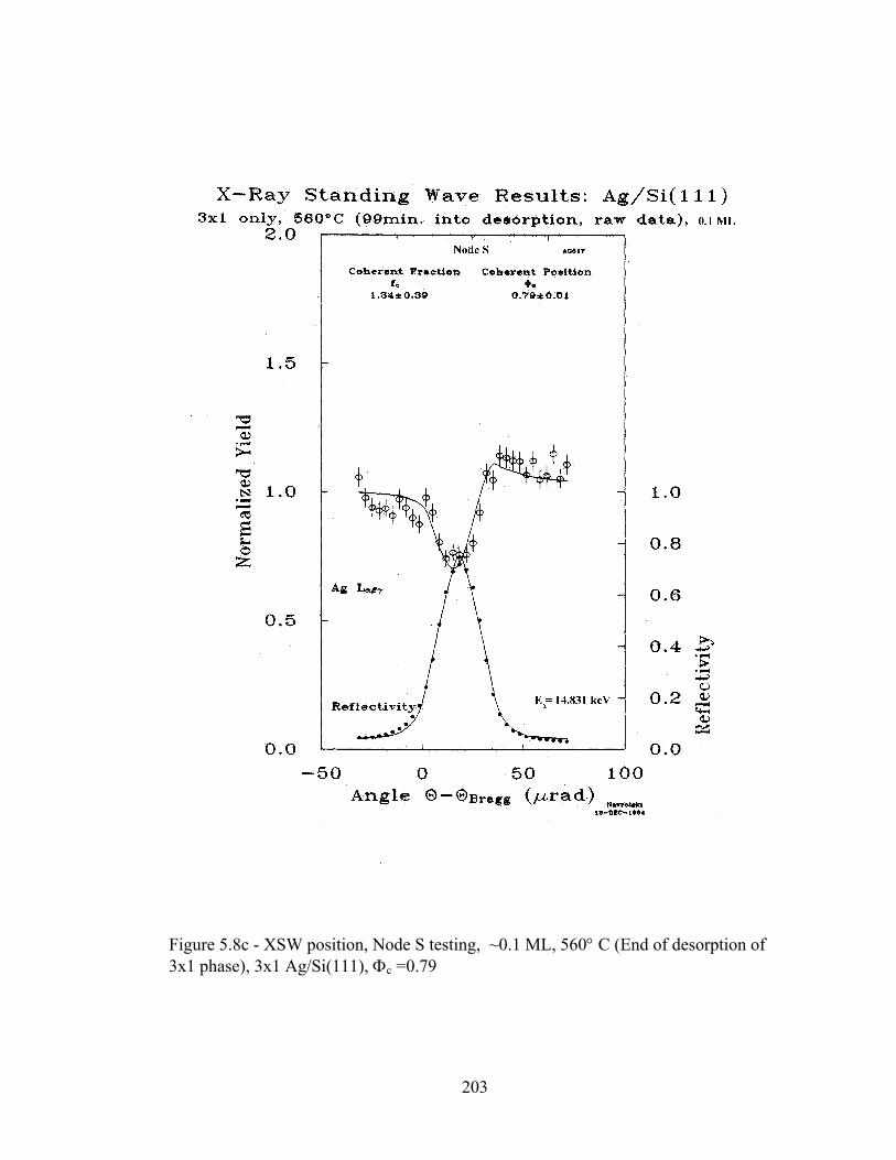
203
Figure 5.8c - XSW position, Node S testing, ~0.1 ML, 560° C (End of desorption of 3x1 phase), 3x1 Ag/Si(111), Φc =0.79

204
Figure 5.9 - XSW results, Node S testing, 0.82 ML Ag/Si(111) at 250°C. Top curve, fluorescent yield, symbols and error bars and theoretical fit. Bottom symbols and curve, measured and fit reflectivity.

205
5.2.2 Node-T testing: C exposed, B exposed, Flat Si(111)
After Node-S testing, all surface Ag had been desorbed as confirmed by AES.
The sample was removed from vacuum, re-Ishizaka/Shiraki etched to create a newly
oxidized surface and re-introduced into vacuum and oxide removal by a 5 minutes at
850°C flash. Numerous attempts were made to create a strictly 3x1 covered surface
at Θ < 0.3 ML. During the process, Ag was deposited and completely desorbed twice
before a good 0.12 ML √3-Ag surface, as measured by LEED at 27 and 42 eV, was
created at 400°C with a measured value of 19.6% carbon (Chapter 3, Equation 18) or
roughly 1.5 x 10¹⁴ C/cm2 (Figure 5.10a). It was noted that the 3x1 structure was
completely inhibited by any presence of carbon on the surface. XSW tests were
completed on this surface as shown in Figure 5.10b and surprisingly, the coherent
fraction, Fc , was still quite high but the coherent position, Φc, for this prototype
surface was quite different than that found for the high coverage prepared surface of
Node-S testing.
Figure 5.10a - Path-dependant XSW measurement, Node T testing. Open circle shows coverage and temperature of sample preparation and measurement reported in Figure 5.10b.

206
Figure 5.10b - XSW Results, Node T testing, 0.13 ML Ag/Si(111). Top curve, fluorescent yield, measured values, error bars and theoretical fit. Bottom symbols and curve, measured values and theoretical fit to reflectivity.

207
5.2.3 Node-U testing: C exposed, B free, Flat Si(111)
Figure 5.11 presents results identical to Node-T testing in terms of coverage
and temperature, obtained from a separately prepared sample cut from a different
portion of the Si(111) sample boule. Carbon levels on this surface were at 0.299 ML
(2.34 x 10¹⁴ C/cm2) with 0.11 ML Ag coverage. Ag coverage was obtained by over-
dosing to 1.96 ML at 400°C then desorbing back to 0.11 ML by holding at 560-
600°C. Again good √3 structure could be seen but 3x1 structure could not be formed
in the presence of this level of carbon contamination.
Figure 5.11a - Path-dependant XSW measurement, Node U testing. Open circle shows coverage and temperature of sample preparation and measurement reported in Figure 5.11b

208
Figure 5.11b - XSW Results, Node U testing, 0.11 ML Ag/Si(111). Top curve, fluorescent yield, measured values, error bars and theoretical fit. Bottom symbols and curve, measured reflectivity.

209
5.2.4 Node-V testing: C free, B free, Flat Si(111)
Figure 5.12 shows the available data for this configuration. Seen in Figure
5.12a, a carbon free surface with sharp 7x7 LEED structure was produced by
Ishizaka/Shiraki oxide removal for five minutes at 920°C. 1.33ML of Ag was
deposited at 400°C and flashed for 11 minutes at 650°C to remove coverage to 0.51
ML with a sharp √3 + faint 3x1 LEED structure. Synchrotron problems allowed only a
few complete XSW and SEXAFS data sets to be taken, as seen by the large error bars
of Figure 5.12b. Additional X-ray flux from the synchrotron source to increase
counting statistics did not become available until after measurable surface
contamination occurred.
With the previously gained knowledge of the profound effect of even slight
carbon contaminations in mind, further work on this sample was abandoned. The
results are included here for completeness along with forced fits for a totally random
array of Ag atoms and a best estimate "χ by eye" fit.
Figure 5.12a - Path-dependant XSW measurement, Node V testing. Open circle shows coverage and temperature of sample preparation and measurement reported in Figure 5.12b

210
Figure 5.12b - XSW Results, Node V testing, 0.5 ML Ag/Si(111). Top curve, fluorescent yield, measured values, error bars and theoretical fit. Bottom symbols and curve, measured values and theoretical fit to reflectivity. Insufficient data for meaningful statistical fits. Dashed theoretical fits are intended as baseline references.
211
5.2.5 Node-W testing: C free, B exposed, 0.5° miscut Si(111)
Results on stepped surfaces were of special interest in light of recent
conjectures that both √3 and 3x1 structures require step edge reconstructions to form
or, in absence of these, create hole-island pairs (essentially an artificial, 1 double-layer
high step). Figures 5.13 show the effect of roughly 30 steps in our experimental
coherence width on surfaces prepared of the same material and using the same
techniques as for Node-S, T, U and V testing.
Surface was prepared by Ishizaka/Shiraki oxide desorption at 890°C for five
minutes producing a sharp 7x7 structure. Ag was deposited on the surface held at
400°C to 0.15-0.2 ML coverage. LEED patterns showed easily attained and sharp Ag-
(√3x√3)R30° and Ag-(3x1) patterns at 78 eV. XSW results show a striking difference
from the flat Si(111) surfaces. Figures 5.13 b. c and d illustrate results at 400°C, 30°C
and 500°C for a combination of √3 and (3x1)-Ag structures at 0.15 ML coverage.
Coherent fractions, Fc are roughly half of values previously seen at coherent
positions, Φc, of between 0.3 and 0.4. Further tests were conducted at 550°C in an
attempt to determine Fc and Φc for the 3x1 phase alone. Total desorption of 0.2ML
occurs in 15 minutes at this temperature so, once again, only a low completeness data
set was collected as shown in Figure 5.13e. By restricting Φc to values between 0.3
and 0.4, a convergence was forced with a fit Fc in agreement with results at other
temperatures. After over two hours at 550°C the spectra of Figure 5.13f was taken
showing that a small random distribution of Ag atoms remains trapped most likely at
step and defect sites as previously noted in the literature. A post-mortem examination
of the surface showed no detectable Ag or carbon contamination.

212
Figure 5.13a - Path-dependant XSW measurement, Node W testing. Open circle shows coverage and temperature of sample preparation and measurement reported in Figure 5.13b, c, d, e, f

213
Figure 5.13b - XSW Results, Node W testing, 0.2 ML Ag/Si(111), 400°C. Top curve, fluorescent yield, measured values, error bars and theoretical fit. Bottom symbols and curve, measured values and theoretical fit to reflectivity.

214
Figure 5.13c - XSW Results, Node W testing, 0.2 ML Ag/Si(111), 30°C. Top curve, fluorescent yield, measured values, error bars and theoretical fit. Bottom symbols and curve, measured values and theoretical fit to reflectivity

215
Figure 5.13d - XSW Results, Node W testing, 0.2 ML Ag/Si(111), 500°C. Top curve, fluorescent yield, measured values, error bars and theoretical fit. Bottom symbols and curve, measured values and theoretical fit to reflectivity
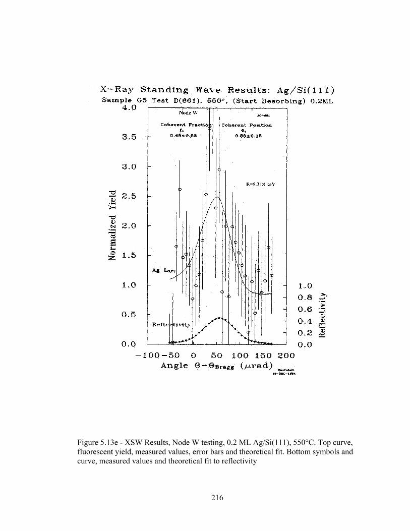
216
Figure 5.13e - XSW Results, Node W testing, 0.2 ML Ag/Si(111), 550°C. Top curve, fluorescent yield, measured values, error bars and theoretical fit. Bottom symbols and curve, measured values and theoretical fit to reflectivity

217
Figure 5.13f - XSW Results, Node W testing, 0 ML Ag/Si(111), 550°C. (after desorption) Top curve, fluorescent yield, measured values, error bars and theoretical fit. Bottom symbols and curve, measured values and theoretical fit to reflectivity

218
5.2.6 Node-X and Y testing: (XSW not done)
5.2.7 Node-Z testing: C free, B free, 0.5° miscut Si(111)
Results from a new sample, prepared exactly as for Node-W testing with the
exception of having wet-chemical cleaning and oxidizing done in borosilicate
glassware is presented in Figures 5.14. Figure 5.14a outlines the preparation path for
the surface at 400°C. LEED showed good √3, 3x1 and 1x1 spots with faint 7x7 spots
remaining. Figure 5.14c is a duplication of the XSW results under the same
conditions as for 5.14b with changes made in x-ray scattering protection and with the
probe beam subtending 4.5X more surface area. The two figures can be considered
indicative of the test-to-test variability of the method if it is assumed that no time
dependent change in surface structure occurs. Further results at 30°C and 500°C are
shown in Figures 5.14d and 5.14e confirming general observations that Ag atomic
positions, Φc do not vary much as a function of temperature once the structure is
formed. Slight increases in coherent fraction, Fc , are seen as temperature decreases,
as expected from Debye-Waller effects.
Figure 5.14a - Path-dependant XSW measurement, Node Z testing. Open circles show coverage & temperature of sample preparation & testing

219
Figure 5.14b - XSW Results, Node Z testing, 0.25 ML Ag/Si(111), 400°C. Top curve, fluorescent yield, measured values, error bars and theoretical fit. Bottom symbols and curve, measured values and theoretical fit to reflectivity

220
Figure 5.14c - XSW Results, Node Z testing, 0.25 ML Ag/Si(111), 400°C. Same conditions as 5.14b with changes in beam conditions. Top curve, fluorescent yield, measured values, error bars and theoretical fit. Bottom symbols and curve, measured values and theoretical fit to reflectivity

221
Figure 5.14d - XSW Results, Node Z testing, 0.25 ML Ag/Si(111), 30°C. Top curve, fluorescent yield, measured values, error bars and theoretical fit. Bottom symbols and curve, measured values and theoretical fit to reflectivity

222
Figure 5.14e - XSW Results, Node Z testing, 0.25 ML Ag/Si(111), 500°C. Top curve, fluorescent yield, measured values, error bars and theoretical fit. Bottom symbols and curve, measured values and theoretical fit to reflectivity

223
REM observations by Yagi200 and STM observations by Wilson and Chiang 201
both confirm that (√3x√3)R30°-Ag selectively forms at step edges. Calculations by
Tong and Huang202 show readily that the (7x7) → (√3x√3) transformation is greatly
facilitated by the presence of a Si(111) double-layer step accommodating the Si self-
adatoms of the 7x7 into an extension of the step edge. It is no surprise that Ag atoms
remain trapped at step defects, Figure 5.13f, even after the remainder of the surface is
Ag free.
5.2.8 Testing of Ag-√3 structures at atmospheric pressures
Tests of (√3x√3)R30°-Ag/Si(111) structures with 31.6, 9.31, 2.16 and 0.48 ML
coverages were done at atmosphere pressure under 99.997% pure He cover gas. (The
cover gas is essential since the three strongest Ag Lα1, Lα2 and Lβ1 fluorescence lines
are easily masked by Ar Kα1, Kα2 and Kβ1 fluorescence lines from the 0.93 vol.% Ar
present in air.) As shown in Figures 5.15, the √3 structure is not preserved once
exposed to the atmosphere, consistent with later findings of Schmitsdorf203 that
surface passivation to oxidation does not hold at greater than 106 Langmuir O2
exposures. Additionally, the √3 Ag/Si(111) surface has been found not to be
preserved when covered with other atmospheric gas layers such a H204 and NO205 at
room temperature . In all cases, only a random distribution of Ag atoms were found
with XSW for these air exposed Ag-(√3x√3)/Si(111) surfaces.

224
Figure 5.15a - XSW Results, Post-mortem bench testing, 31.6 ML Ag/Si(111), R.T. Top curve, fluorescent yield, measured values, error bars and theoretical fit. Bottom symbols and curve, measured values and theoretical fit to reflectivity

225
Figure 5.15b - XSW Results, Post-mortem bench testing, 9.3 ML Ag/Si(111), R.T. Top curve, fluorescent yield, measured values, error bars and theoretical fit. Bottom symbols and curve, measured values and theoretical fit to reflectivity

226
Figure 5.15c - XSW Results, Post-mortem bench testing, 2.16 ML Ag/Si(111), R.T. Top curve, fluorescent yield, measured values, error bars and theoretical fit. Bottom symbols and curve, measured values and theoretical fit to reflectivity

227
Figure 5.15d - XSW Results, Post-mortem bench testing, 0.48 ML Ag/Si(111), R.T. Top curve, fluorescent yield, measured values, error bars and theoretical fit. Bottom symbols and curve, measured values and theoretical fit to reflectivity

228
5.2.9 Summary of XSW results
XSW results are tabulated, along with reduced χ2 indications of goodness of fit
in Table 5-1.
Table 5.1 - Summary of XSW findings for Ag/Si(111)Table 5-1: Summary of XSW findings for Ag/Si(111)
Fc = coherent fraction, Φc = coherent position Node Figure Θ Temp. Fc Φc χ2
S 5.7b 2.58 400°C 1.09 ± 0.33 0.79 ± 0.02 0.40 S 5.9 0.82 250°C 0.94 ± 0.17 0.20 ± 0.02 75.4 T 5.10b 0.13 400°C 1.01 ± 0.06 0.69 ± 0.01 2.40 U 5.11b 0.11 400°C 0.97 ± 0.15 0.69 ± 0.02 0.68 V 5.12b 0.5 400°C --- --- --- W 5.13b 0.2 400°C 0.29 ± 0.11 0.40 ± 0.05 0.20 W 5.13c " 30°C 0.51 ± 0.18 0.37 ± 0.04 0.22 W 5.13d " 500°C 0.46 ± 0.14 0.30 ± 0.03 0.44 W 5.13e " 550°C 0.45 ± 0.52 0.38 ± 0.15 0.16 Z 5.14b 0.25 400°C 0.82 ± 0.18 0.33 ± 0.02 0.21 Z 5.14c " 400°C 0.83 ± 0.09 0.36 ± 0.01 0.64 Z 5.14d " 30°C 1.00 ± 0.12 0.37 ± 0.01 0.59 Z 5.14e " 500°C 0.50 ± 0.12 0.39 ± 0.03 0.24

229
5.3 SEXAFS Bond Length Measurements
As outlined in Chapter 3, the Surface Extended X-ray Absorption Fine
Structure (SEXAFS) technique can be used, as a first approximation, to determine
atom-pair-specific bond lengths to within 4% and nearest-neighbor coordination to
within 20%. Bond length results reported here can be confidently inter-compared
since all contain the same error contributions from experimental and analytical
methods. For absolute bond length measurements, careful propagation of errors
indicates ± 0.05 Å accuracy level. In this research, no attempt was made to
determination coordination number and second nearest neighbor bond lengths.
X-ray Fine Structure (XFS) analysis in the Ag/Si system suffers from the lack
of a reference material with known Ag-Si bond length to be used for the
backscattering amplitude and phasing correction components of the data analysis.
Following suggestions of Stöhr and Jaeger206 the experimentally determined
corrections were taken from Pd2Si as a model compound. It was hoped that the
electronic structure of Pd, being only one 5s1 electron different than Ag, would
provide the same correction factors since the core-potentials, the essential component
for electron backscattering effects, should be for all purposes the same. One great
advantage of this work over that of Stöhr and Jaeger’s comes from the ability to study
K-edge absorption structure rather than LIII edge. Curved-wave electron wavefront
propagation analysis and scattering is difficult enough for electrons with s-like
character. Introducing p- and d- like character to the outwardly propagating wave can
not yet be taken into account and is such complexity is usually ignored.
Experimentally, the sample fluorescence signal, Ag Kα1 and Kα2 at 22.163
and 21.990 keV respectively (Kαave=22.104 keV) is monitored through the re-entrant
Be window snout with a Si(Li) detector. The electronic signal is amplified and

230
windowed to produce a signal to background count coincident with scanning of the
incident X-ray energy through the Ag K absorption edge at 25.514 keV.
An inherent problem with Ag K edge XFS (X-ray Fine Structure) comes about
due to interference by Compton scattered X-rays. First, the relatively high energy of
the edge, 25.514 keV, and correspondingly short wavelength increases the Compton
shift. Secondly, it is desirable to look along the polarization vector of the incident
synchrotron bending magnet beam and there are constraints of the vacuum system
such that the fluorescence signal is detected at 90° from the incident X-ray beam. The
magnitude of the problem is illustrated in Figure 5.16 where Compton shifts at various
incident energies are plotted over the energy range of a typical XFS scan. It can be
seen by the figure to the right, that the Ag Kα signal from 1 ML in σ polarization
geometry has a signal/noise ratio of only about 0.1 making counting times at X-ray
fluxes of 1011 photons/sec incident, quite long for even 5% counting statistics.
An additional difficulty arises due to the peculiar behavior of small signals on
sloping backgrounds. In the experimental case here, a narrow electronic window was
placed around the Ag Kα1,2 peak and additional windows are placed above and below
that signal window for background measurement and subtraction. In practice, the
“signal” window is set by fluorescing the Ag standard, a strong signal, and setting
windows to capture the appropriate signal and background channels. When
measurements are made with a weak signal on a strongly sloping signal, the apparent
signal maximum moves “up hill” from its “true” position. This shift is proportional to
the signal (FWHM)2 x (Background slope) and inversely proportional to the signal
strength207. In essence, useful signal is pushed into the upper background signal
window and lost.
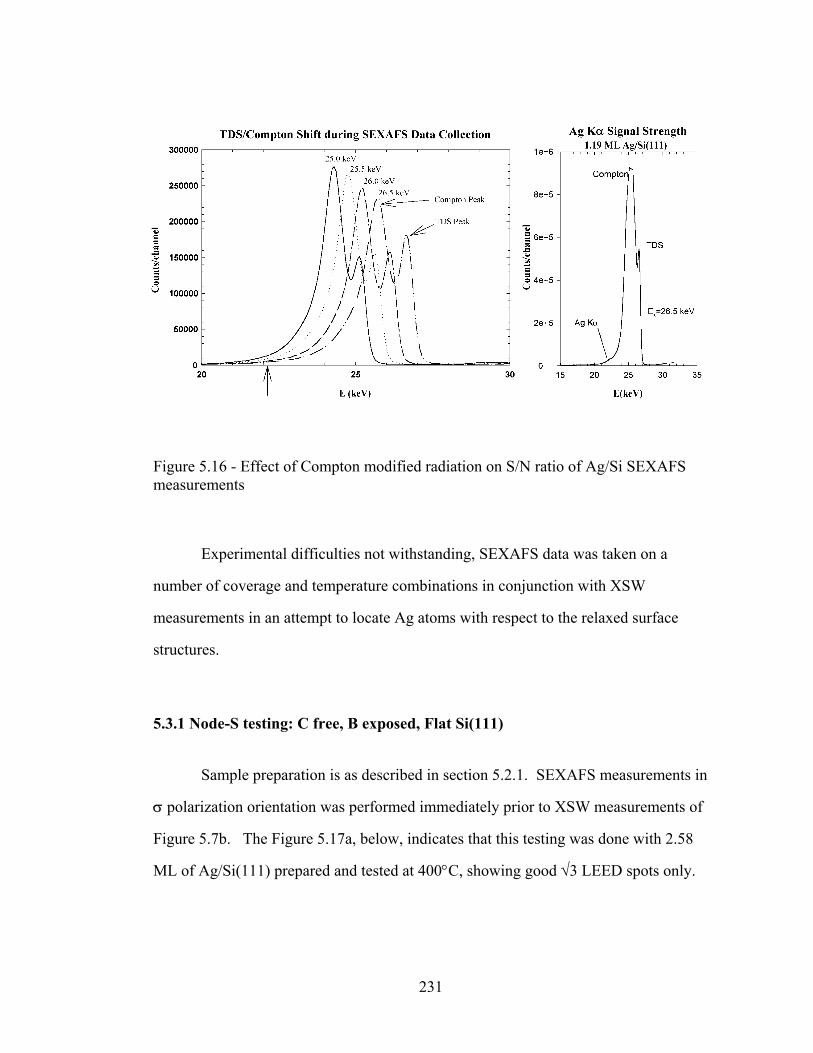
231
Figure 5.16 - Effect of Compton modified radiation on S/N ratio of Ag/Si SEXAFS measurements
Experimental difficulties not withstanding, SEXAFS data was taken on a
number of coverage and temperature combinations in conjunction with XSW
measurements in an attempt to locate Ag atoms with respect to the relaxed surface
structures.
5.3.1 Node-S testing: C free, B exposed, Flat Si(111)
Sample preparation is as described in section 5.2.1. SEXAFS measurements in
σ polarization orientation was performed immediately prior to XSW measurements of
Figure 5.7b. The Figure 5.17a, below, indicates that this testing was done with 2.58
ML of Ag/Si(111) prepared and tested at 400°C, showing good √3 LEED spots only.

232
Figure 5.17a - Path dependant sample preparation, coverage and phase for Node-S SEXAFS measurements. Open circle depicts coverage and temperatures of measurements of Figure 5.17b
As shown in Figure 5.17b, each of the three peaks A’, A and B were filtered,
transformed and phase adjusted using the Pd2Si reference standard and using FEFF208
or McKale209 theory. Differences in predictions were within experimental variances.
From McKale theory, dual distances for Ag-Si bond lengths of 2.2 and 2.5Å were
determined for peaks A’ and A respectively. Stöhr and Jaeger206 found a similar A-
A’ pair and explained it as a splitting due to a Ramsauer-Townsend resonance in the
backscattering amplitude as explained in Mott and Massey.210 An Ag-Ag bond length
of 3.27Å was determined for peak B, a value 13% larger than the bulk Ag-Ag
distance of 2.9Å. Peak X appears in all of the fluorescence measurements and is a
systematic artifact of the background fitting and subtraction method used for all data
analysis.

233
Figure 5.17b - Node S SEXAFS measurement, 2.58 ML Ag/Si(111)- 400 °C (top) fluorescence signal, (middle) Chi function and fit from atom-pair shown in (bottom) radial distribution function with Hanning filter window.

234
5.3.2 Node-T testing: C exposed, B exposed, Flat Si(111)
Sample preparation is as described in section 5.2.2. SEXAFS measurements in
σ, 45° and π polarizations were performed immediately concurrent with XSW
measurements of Figure 5.10b. The Figure 5.18a, below, indicates that this testing
was done with 0.12 ML of Ag/Si(111) prepared and tested at 400°C, showing good √3
LEED spots only and a measured 19.3% C contamination. Numerous anneal cycles
from 400° to 600° and back were done in an attempt to create a 3x1 structure. An
anecdotal reference later discovered in the literature and confirmed by this research
confirms that the Ag-(3x1)/Si(111) structure will not form in the presence of
measurable carbon contamination even though the Si(111) surface prior to Ag
deposition shows good 7x7 structure.
Figure 5.18a - Sample preparation, coverage and phase for Node-T SEXAFS measurements. Open circle depicts coverage and temperatures of duplicate measurements shown in Figure 5.18b and 5.18c.
Results from σ polarization tests indicate a 2.1 to 2.2Å Ag-Si bond length,
peak A’. Lengths for the A peak, Ag-Si bond as fit to 2.6. Peak C fits, modeled by
phase shifts of an Ag-Ag bond pair, refines to an interatomic distance of 3.1Å
assumed to be an in-plane second-nearest neighbor vector.

235
Figure 5.18b - Node T SEXAFS measurement, 0.12 ML Ag/Si(111)- 400 °C Wide slits (.5mm v x 5mm h) for large surface area averaging. Curves (top) fluorescence signal, (middle) Chi function and fit from atom-pair shown in (bottom) radial distribution function with Hanning filter window

236
Figure 5.18c - Node T SEXAFS measurement, 0.12 ML Ag/Si(111)- 400 °C Narrow slits (.5mm v x 1mm h) for small surface area averaging. Curves; (top) fluorescence signal, (middle) Chi function and fit from atom-pair shown in (bottom) radial distribution function with Hanning filter window

237
5.3.3 Node-U testing (No SEXAFS testing done)
5.3.4 Node-V testing: C free, B free, Flat Si(111)
Sample preparation, detailed in Section 5.2.4, producing a sharp √3 structure
only at 0.51 ML coverage is illustrated in Figure 5.19a. SEXAFS data in σ and π
polarizations were taken immediately after the XSW data of Figure 5.12b at 400°C.
Figure 5.19a - Path-dependant SEXAFS measurement, Node V testing. Starting at 1.33 ML dose, sample preparation is shown by solid line. Open circle shows coverage and temperature of measurement reported in Figure 5.19b,c .
The dominant A’ peak in the π “surface normal direction” polarization, Figure
5.19b, is fit with McKale theory to 1.4Å Ag-Si distance. Data for the σ “in plane”
polarization, Figure 5.19c, is either of too poor a quality to analyze (see section 5.2.4
for description of synchrotron problems) or actually has multiple, amorphous like,
multi bond-length distances without a dominant first near-neighbor.

238
Figure 5.19b - Node V SEXAFS measurement π polarization, 0.51 ML Ag/Si(111)- 400 °C (top) fluorescence signal, (middle) Chi function and fit from atom-pair shown in (bottom) radial distribution function with Hanning filter window

239
Figure 5.19c - Node V SEXAFS measurement σ polarization, 0.51 ML Ag/Si(111)- 400 °C (top) fluorescence signal, (middle) Chi function and fit from atom-pair shown in (bottom) radial distribution function with Hanning filter window

240
5.3.5 Node-W testing: C free, B exposed, 0.5° miscut Si(111)
Immediately following the XSW measurements of Section 5.2.5, the sample
surface remained carbon free and showed slight residual random located Ag (Figure
5.13f). This remaining adsorbate was removed by a five minute, 800°C flash then re-
deposition with Ag to 1.35ML coverage at 400°C. SEXAFS measurements were made
at this high coverage (√3 structure only) then at 0.15 ML coverage (both √3 and 3x1
structures) produced by multiple annealing cycles to 700°C as outlined in Figure
5.20a.
Figure 5.20a - Path-dependant SEXAFS measurement, Node W testing. Starting at 1.33 ML dose, sample preparation is shown by solid line. Open circle shows coverage and temperature of measurement reported in Figure 5.20b,c
Results of π polarization measurements, Figure 5.20b, shows a dominating A
peak at 2.0 Å. Equivalent σ measurement, Figure 5.20c shows the amorphous-like,
multi-peaked radial distribution function as in the previous section.

241
Figure 5.20b - Node W SEXAFS measurement π polarization, 1.35 ML Ag/Si(111)- 400 °C (top) fluorescence signal, (middle) Chi function and fit from atom-pair shown in (bottom) radial distribution function with Hanning filter window

242
Figure 5.20c - Node W SEXAFS measurement σ polarization, 0.15 ML Ag/Si(111)- 400 °C (top) fluorescence signal, (middle) Chi function and fit from atom-pair shown in (bottom) radial distribution function with Hanning filter window

243
5.3.6 Node-X and Y testing: (SEXAFS not done)
5.3.7 Node-Z testing: C free, B free, 0.5° miscut Si(111)
Immediately before and after the XSW testing of Section 5.2.7, Figures
5.14b,c,d,e, SEXAFS measurements were taken. Initially, a coverage of 0.25 ML,
good √3 and (3x1) along with (1x1) and faint (7x7) LEED spots indicated, shown in
Figure 5.21a, provided the radial distribution functions of Figure 5.21b with Ag-Si
distance, peak B, of 2.8 Å.
Figure 5.21a - Path-dependant SEXAFS measurement, Node Z testing. Starting at 0.6 ML dose, sample preparation is shown by solid line. Dashed line indicates structure and coverage change after 24 hour hold in UHV. Open circle shows coverage and temperature of measurement reported in Figure 5.21b,c and d
The synchrotron x-ray source experienced an unplanned down period. After
holding the sample at 400°C for 24 hours, minimum detectable carbon contamination
of 0.02ML was found with loss of the 3x1 LEED pattern and apparent desorption, or
redistribution, of Ag to the 0.1 ML level. SEXAFS measurements after this minuscule
surface contamination in both π and σ geometries are presented in Figures 5.21c and d
respectively.

244
Figure 5.21b - Node Z SEXAFS measurement π polarization, 0.25 ML Ag/Si(111)- 400 °C (top) fluorescence signal, (middle) Chi function and fit from atom-pair shown in (bottom) radial distribution function with Hanning filter window

245
Figure 5.21c - Node Z SEXAFS measurement π polarization, 0.1 ML Ag/Si(111)- 400 °C (top) fluorescence signal, (middle) Chi function and fit from atom-pair shown in (bottom) radial distribution function with Hanning filter window

246
Figure 5.21d - Node Z SEXAFS measurement σ polarization, 0.1 ML Ag/Si(111)- 400 °C (top) fluorescence signal, (middle) Chi function and fit from atom-pair shown in (bottom) radial distribution function with Hanning filter window

247
5.3.8 Summary of SEXAFS results
Ag-Si and Ag-Ag bond length results from Figures 5.17 thru 5.21 are compiled
in Table 5.2 below. In many cases, the individual single-shell filtered, back-
transformed and fit results using either a Pd2Si reference standard or theoretical
spherical wave amplitude and phase shift functions calculated by Rehr’s FEFF208
method or McKale’s209 method are included. Clearly, bond lengths from π
polarization measurements which enhance surface normal bond orientations, are much
shorter than the σ or in-plane measurements.

248
Table 5.2 - Summary of SEXAFS findings for Ag/Si(111)Table 5.2: Summary of SEXAFS findings for Ag/Si(111)
All data at 400°C A’, A = Ag-Si nearest neighbor bond lengths;
B= second nearest neighbor bond length (Ag-Ag or Ag-Si) Node Figure Θ Pol. Peak A’ Peak A Peak B
S
5.17b 2.58 σ 2.2 Å 2.5 Å 3.3 Å(Ave.) 2.97 ± 0.04 Pd2Si 3.46 ± 0.02 FEFF 3.38 ± 0.01 McKale
T
5.18b 0.12 σ 2.2 Å(Ave.) 1.92 ± 0.03 Pd2Si 2.34 ± 0.01 FEFF 2.24 ± 0.01 McKale
2.6 Å 3.1 Å
T
5.18c 0.12 σ 2.1 Å(Ave.) 1.83 ± 0.03 Pd2Si 2.26 ± 0.02 FEFF 2.18 ± 0.01 McKale
--- ---
U --- 0.10 --- ---
---
V
5.19b 0.51 π 1.4 Å 1.19 ± 0.03 Pd2Si
1.9 Å 2.7 Å
V
5.19c 0.51 σ (1.8) (2.2) (3.0) 2.91 ± 0.06 Pd2Si
W
5.20b 1.35 π 2.2 Å 2.02 ± 0.03 Pd2Si 2.32 ± 0.01 McKale
--- ---
X
5.20c 0.15 σ --- --- ---
Z
5.21b 0.25 π 1.8 Å 2.2 Å 2.8 Å and 3.4 Å
Z
5.21c 0.10 π 1.5 Å(Ave.) 1.28 ± 0.03 Pd2Si 1.72 ± 0.04 FEFF 1.63 ± 0.04 McKale
2.1 Å 2.8 Å
Z
5.21d 0.10 σ 1.4 Å 2.0 Å 2.8 Å(Ave.) 2.48 ± 0.04 Pd2Si 2.98 ± 0.01 FEFF
2.87 ± 0.01 McKale

249
5.4 References - Chapter Five 184 F. Wehking, H. Beckermann and R. Niedermayer Surf. Sci. 71, 364 (1978). 185 D. Bolmont, P. Chen, C.A. Sebenne and F. Proix, Phys. Rev. B 24, 4552 (1981). 186 V.A. Grazhulis, Appl. Surf. Sci. 33/34, 1 (1988). 187 M. Hanbücken, H. Neddermeyer and P. Rupieper, Thin Solid Films, 90, 37 (1982). 188 E.J. Van Loenen, M. Iwami, R.M. Tromp and J.F. Van Der Veen, Surf. Sci. 137, 1 (1984). 189 S. Kohmoto and A. Ichimiya, Appl. Surf. Sci. 33/34, 45 (1988). 190 M. Housley, R. Heckingbottom and C.J. Todd, Surf. Sci. 68, 179 (1977). 191 E. Bauer and H. Poppa, Thin Solid Films 12, 167 (1972). 192 G. LeLay, A. Chauvet, M. Manneville and R. Kern, Appl. Surf. Sci. 9, 190 (1981). 193 Y. Gotoh, A. Chauvet, M. Manneville and R. Kern, Jpn. J. Appl. Phys. 20, L853 (1981). 194 G. LeLay, M. Manneville and R. Kern, Surf. Sci. 72, 405, (1978).
195 M. Saitoh, F. Shoji, K. Oura and T. Hanawa, Surf. Sci. 112, 306, (1981). 196 H.H. Weitering, N.J. DiNardo, R. Perez-Sandoz, J. Chen and E.J. Mele, Phys. Rev. B, 49, 16837-16840 (1994). 197 A. Cros, F. Houzay, G.M. Guichar and R. Pinchaux, Surf. Sci. 116, L232 (1982). 198 J. Youhar, M. Inoue and K. Morita, J. Vac. Sci. Technol. A 11, 2714 (1993). 199 R. Kern and G. LeLay, J.Phys. (Paris) 60, C4-155 (1977). 200 K. Yagi, N. Osakabe, Y. Tanishiro and G. Honjo, Proceedings of the 4th International Conference on Solid Surfaces and 3rd European Conference on Surface Science, edited by D.A. Degras and M. Costa (Cannes, France) 2, 1007, (1980). 201 R.J. Wilson and S. Chiang, Phys. Rev. Let. 59, 2329 (1987).
250
202 S.Y. Tong and H. Huang, Surf. Sci. Let. 243, L46 (1991). 203 R.F. Schmitsdorf, T.U. Kampen and W. Mönch, Surf. Sci., 324, 249 (1995). 204 T. Kinoshita, Y. Tanaka, K. Sumitomo, F. Shoji, K. Oura and I. Katayama, Appl. Surf. Sci. 60, 183 (1992). 205 S. Glass, E.W. McFarland, H. Nienhaus, Surf. Sci. 518, 133-140 (2002). 206 J. Stöhr and R. Jaeger, J. Vac. Sci. Technol. 21, 619 (1982). 207 A.H. Benade, Reference notes on the collection and treatment of data, Case Western Reserve University, Department of Physics, 1968. 208 J.J Rehr and E.A. Stern, Phys. Rev. B 11, 4413 (1976). 209 A.G. McKale, B.W. Veal, A.P. Paulikas, S.K. Chan and G.S. Knapp, J. Am. Chem. Soc. 110, 3763 (1988). 210 N.F. Mott and H.S.W. Massey, The Theory of Atomic Collisions (third edition), Oxford at the Clarendon Press, 1965.
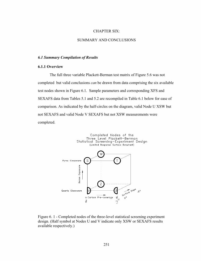
251
CHAPTER SIX:
SUMMARY AND CONCLUSIONS
6.1 Summary Compilation of Results
6.1.1 Overview
The full three variable Plackett-Berman test matrix of Figure 5.6 was not
completed but valid conclusions can be drawn from data comprising the six available
test nodes shown in Figure 6.1. Sample parameters and corresponding XFS and
SEXAFS data from Tables 5.1 and 5.2 are recompiled in Table 6.1 below for ease of
comparison. As indicated by the half-circles on the diagram, valid Node U XSW but
not SEXAFS and valid Node V SEXAFS but not XSW measurements were
completed.
Figure 6. 1 - Completed nodes of the three-level statistical screening experiment design. (Half symbol at Nodes U and V indicate only XSW or SEXAFS results available respectively.)

252
Notes: * Minimum carbon detection limit, 3.0 x 10¹³ C/cm2 or 0.038 ML 3D = 3D Ag islands on Ag-(√3x√3) σ, π = in-plane or out-of-plane polarization measurement states Values in ( ) are general indications only and not strictly statistically valid
Table 6.1: Summary of Sample Preparation, XSW and SEXAFS findings for Ag/Si(111)
Sample Parameters XSW SEXAFS Node B
? C*
(ML) Cut Θ
(ML) Temp(°C)
Structure Fc
(fraction) Φc
(position) Pol. A’ A B
2.58 400°C √3 + 3D 1.09 0.79 ± 0.02 σ 2.2 Å 2.5 Å 3.3 Å S Y 0 0° 0.82 250°C √3 (0.94 0.20±0.02) --- --- --- ---
~0.13 400°C √3 1.01 0.69 ± 0.01 σ 2.2 Å 2.6 Å 3.1 Å T Y .19 0° 0.12 400°C √3 --- --- σ 2.1 Å --- ---
U N .30 0° 0.11 400°C √3 0.97 0.69 ± 0.02 --- --- --- --- V N 0 0° 0.51 400°C √3 --- (~0.2 ) π 1.4 Å 1.9 Å 2.7 Å
1.35 400°C √3 + 3D --- --- π --- 2.2 Å --- 400°C √3 + 3x1 0.29 0.40 ± 0.05 --- --- --- --- 30°C √3 + 3x1 0.51 0.37 ± 0.04 --- --- --- --- 500°C √3 + 3x1 0.46 0.30 ± 0.03 --- --- --- ---
W Y 0 0.5° 0.2
550°C √3 + 3x1 0.45 0.38 ± 0.15 --- --- --- --- 400°C √3 + 3x1 0.82 0.33 ± 0.02 π 1.8 Å 2.2 Å 2.8 Å
3.4 Å 400°C √3 + 3x1 0.83 0.36 ± 0.01 --- --- --- ---
30°C √3 + 3x1 1.00 0.37 ± 0.01 --- --- --- ---
0.25
500°C √3 + 3x1 0.50 0.39 ± 0.03 --- --- --- --- --- --- π 1.5 Å 2.1 Å 2.8 Å
Z N 0 0.5°
0.10 400°C √3 + 3x1 --- --- σ 1.4 Å 2.0 Å 2.8 Å

253
The following general observations can be made from the Table 6.1 for the
clean surfaces. First, at low-elevated temperatures, 250°C and a capping coverage of
0.82 ML (Node S) Ag sits deeply embedded among the Si(111)-(7x7) self-adatoms at
coherent position of Φc =0.20. In the high-elevated temperature regime, 400°C, and at
low coverage, 0.2 ML (Node W & Z), Ag atoms begin to replace the Si self-adatoms.
Since Ag atoms are insufficient in number to satisfy surface reconstruction needs, Si
self-adatoms remain essential to the surface structure placing Ag at coherent position
of Φc =~0.37. Processing by over deposition and desorption back to low coverages
increases coherent fraction (aligns Ag atoms better) than deposition at the exact 0.2
ML coverage studied but does not change the Ag atom locations.
Under the same elevated temperature conditions, 400°C, either C
contamination or fully saturated Ag coverage satisfies surface dangling bonds
allowing Ag to sit at a coherent position Φc =0.69 (C) or Φc =0.79 (Ag) from surface.
Both scenarios produce well ordered Ag-√3 layers with high coherent fraction.
6.1.2 Boron Exposure
There is no effect from boron contamination by chemical processing in
borosilicate (Pyrex™) glassware. (The reader is reminded that all other sources of B
contamination; vacuum system viewports, boron nitride vacuum components,
borosilicate glass insulators, etc. were all systematically eliminated as contributing
factors.) Figure 6.2 compares node W and node Z XSW results (0.5° vicinal surfaces,
C free, ~0.2 ML Ag at 30°C) with and without B exposure. No statistically significant
differences in coherent position, Φc is seen. There is, however, significant difference
in the coherent fraction, Fc , with the boron free surface exhibiting almost unity
coherence. This is thought to be a path dependant surface preparation effect rather
than a boron effect as will be elaborated on later. Similar results can be seen by

254
comparing like node W and Z results at 400°, 500° and 550°C. Bond lengths for the
low coverage, low coherent fraction, node W experiments were not quantifiable and,
in fact, seemed amorphous like. The node W, 1.35 ML, high coverage π polarization
measurement shows the predominant 2.2 Å Ag-Si bond length. Comparable node Z
bond lengths repeated the 2.2 Å length in addition to an almost unphysical 1.4 – 1.8 Å
Ag-Si length and a 2.8Å Ag-Ag length.
Likewise, test nodes T and U can be directly compared as shown in Figure 6.3.
No B effect is seen in these samples, both are flat surfaces, C contaminated (0.3 and
0.2 ML C respectively), ~0.2 ML Ag at 400°C. Node T Ag-Si bond lengths are
consistently of 2.2 and 2.6 Å with an additional Ag-Ag length of ~3.2 Å. These are
distances that will be shown to characteristically repeat for surfaces where the surface
dangling bonds are satisfied by methods such as complete, ~ 1 ML Ag coverage or
high, >.2 ML, carbon contamination.
As an aside, both moderate coverage, 0.8 and 0.5 ML nodes S and V
(respectively) XSW tests, although statistically invalid, show indications of roughly
the same Ag atomic positions at Φc =0.2.

255
Figure 6.2 - XSW measurement; effect of B exposure on nominal positions of 3x1 + √3x√3R30° Ag/Si(111) phases. Filled symbols, Node W (from Figure 5.13c). Open symbols, Node Z (from Figure 5.14d). Solid lines, theoretical fits to Rocking Curve and Coherent Position.

256
Figure 6. 3 - XSW measurement; effect of B exposure on nominal positions of √3x√3R30° Ag/Si(111) phase. Filled symbols, Node T (from Figure 5.10b). Open symbols, Node U (from Figure 5.11b). Solid lines, theoretical fits to Rocking Curve and Coherent Position.

257
With a null result for the Boron variable, we can straightforwardly reduce the
dimensionality of the experimental matrix in a way that would have been done
statistically if experimental results were available for all test nodes. That is, the test
matrix can now be represented by the planar projection of the full test matrix along the
boron axis into the two variable system of Figure 6.4.
Figure 6.4 - Reduced dimensionality test matrix removing Boron null test result.
6.1.3 Evaluation of the reduced test matrix
It is immediately apparent from Figures 6.2 and 6.3 that there is a major
outward shift in Ag atomic positions of approximately 0.32 dSi(111) , almost 1Å, in the
<111> direction between the, C free, flat surface, regardless of B, and the C
contaminated, 0.5° vicinal surface, regardless of B. It is also apparent that there is an
associated bond length change, speaking roughly; from the range of 1.4 -1.8Å to 2.2 Å
for the A’ peak, from 2.1 Å to 2.5Å for the A peak, and from 2.8 Å to 3.2 Å for the

258
B peak as schematically illustrated in Figure 6.5. So the immediate question becomes,
which variable or variable combination is dominant?
Figure 6. 5 - Schematic model illustration of atomic arrangements in A) Node W or Z Φc and bond lengths and B) Node T or U Φc and bond lengths.
First, the reader must be careful to compare only like-results from summary
Table 6.1, above. Reliable node S, XSW and SEXAFS results are only available for
high, 2.58 ML coverage. Node W SEXAFS results are only available, again, for high
1.35 ML coverage. Both sets of results must be excluded from the discussion to
ascertain which, or what combination of carbon and boron are responsible for the
surface shifts for the following reason. It is conjectured that the profound changes that
accompany the transformation of the clean Si(111)-(7x7) DAS surface to the Ag-β-
(√3x√3)R30°/Si(111) surface are complete at the 2/3 ML Ag deposition levels for
temperatures between 200° and 400°C. It is also conjectured that the profound
changes that accompany the transformation of this surface to the Ag-γ-(√3x√3)R30°
/Si(111) surface are complete at the 1 ML Ag deposition levels for temperatures above
400°C. It is known, that these changes include the mass rearrangement of the 7x7
“self-adatoms” above 200°C, satisfaction of the bulk-like 1x1 surface dangling bonds
and possibly the correction of the surface stacking fault at temperatures above 400°C
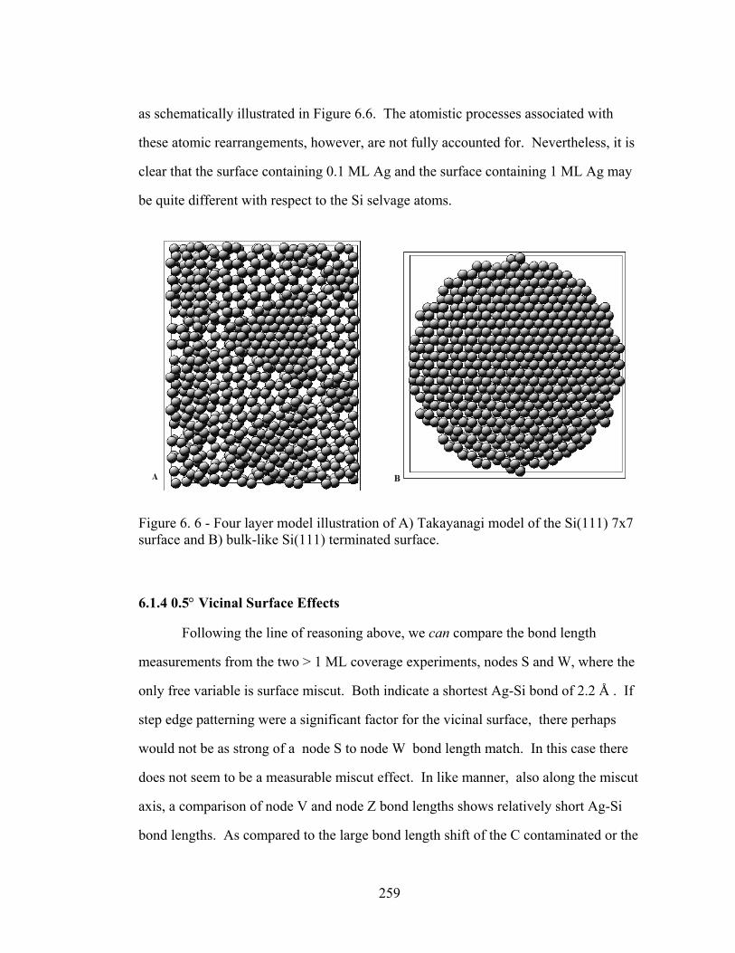
259
as schematically illustrated in Figure 6.6. The atomistic processes associated with
these atomic rearrangements, however, are not fully accounted for. Nevertheless, it is
clear that the surface containing 0.1 ML Ag and the surface containing 1 ML Ag may
be quite different with respect to the Si selvage atoms.
Figure 6. 6 - Four layer model illustration of A) Takayanagi model of the Si(111) 7x7 surface and B) bulk-like Si(111) terminated surface.
6.1.4 0.5° Vicinal Surface Effects
Following the line of reasoning above, we can compare the bond length
measurements from the two > 1 ML coverage experiments, nodes S and W, where the
only free variable is surface miscut. Both indicate a shortest Ag-Si bond of 2.2 Å . If
step edge patterning were a significant factor for the vicinal surface, there perhaps
would not be as strong of a node S to node W bond length match. In this case there
does not seem to be a measurable miscut effect. In like manner, also along the miscut
axis, a comparison of node V and node Z bond lengths shows relatively short Ag-Si
bond lengths. As compared to the large bond length shift of the C contaminated or the

260
high coverage surfaces, again, a minimal miscut effect. For these reasons, surface
steps at this density level is thought to play a minor roll, if any, in the positioning of
Ag √3 or 3x1 phases.
Most likely, it is not the fact that low step density (0.5° miscut) versus flat (0°
miscut) shows no effect but rather that Ag deposits create pseudo-steps in the form of
hole-island groups when natural step imperfections are not present. The act of
sweeping Si(111)-(7x7) self-adatoms away by Ag deposits creates sinks to store these
displaced Si atoms in lieu of insufficient storage space at naturally occurring defect
sites.
6.1.4 Carbon Effect
Carbon is supremely good at modifying the 7x7 surface and satisfying
dangling bonds better than Si or Ag adatoms. Silver, on the other hand, is a very
weakly bonding species and for most intents and purposes is must be available in
large, almost 1:1 quantities with the Si atoms to achieve the same surface modification
effects. The effect of 0.2 ML C (as calculated by the conservative Seah equation,
Chapter 3 equation 18) is equivalent to that of nearly a complete monolayer of Ag.
Supporting this assertion is anecdotal evidence presented in Chapter 5 as well
as in the literature that the Ag-(3x1) structure can not be formed in the presence of C
contamination. Additionally, others have quantified profound changes in the S-K
growth mode and Ag(111) crystallite morphology at extremely high (hundreds of Å)
coverage levels as a correlated with surface C contamination. All of these clues point
to a C effect rather than a step effect as dominant.
Unfortunately, inexorably linked to this carbon effect is the mixed structure
effect. That is, at low coverage, one can not form √3 + (3x1) mixed phase with C
contamination and, conversely, one can not avoid forming this mixed phase on clean

261
surfaces by the desorption processing technique used in this study. Low and
intermediate coverage deposits at temperatures less than 500°C, where only √3
structure is created, were not quantitatively successful within the experimental time
available.
Carbon is an excellent Si(111) surfactant. As surface scientists we eschew C
on the surface as contamination and have spent considerable effort to find suitable
surfactants like Sb and Br that promote F-M, layer-by-layer growth. The role of C
must be explored.
6.1.5 Surface Coverage / Surface Effect
An unexpectedly dominant effect proposed here as controlling the Ag-Si bond
length as well as ensemble average position is total surface coverage. The higher the
deposited Ag surface coverage, the more the Si(111)-(7x7) self-adatom layer is
modified and bulk-like Si surface dangling bonds are satisfied.
This effect is implied by the following observations. Differences in the
coherent fraction, Fc but not position, Φc between results of node W and node Z (B
vs. no-B) can be explained as proposed, by surface coverage effects. The preparation
methods used to get to the same 0.2 ML Ag/Si test point were different illustrating the
path dependence of this surface structure. For the node W surface, Ag was deposited
on clean Si-(7x7) surface at exactly the 0.2 ML test coverage. Coherent fractions were
low although coherent positions, Φc were equivalent to node Z tests. The node Z
surface started with Ag depositions at a higher coverage, 0.6 ML, before reducing Ag
to the 0.25 ML test coverage via surface desorption. The initial 7x7 adatom structure
at least on the faulted half of the DAS 7x7 structure was swept away by this process
before being re-formed in the desorption/rearrangement process.
262
6.1.6 Comparison to existing structural models
If we compare the experimental results of Table 6.1 with the model structure
parameters of Table 2.3 we can make the correlations summarized in Table 6.2. First,
for a fully developed, ≥ 1 ML Ag-(√3x√3)R30°/Si(111) structure or a surface
contaminated with C, both of which completely replace Si self-adatoms to satisfy
surface dangling bonds, the three indicators of surface contraction, multiple Ag-Si
bond lengths and Ag-Ag bond lengths are fully consistent with the HCT-8 model of
Takahashi (CN252). In this model, Ag-Si bond length in the radial and side
directions, as referenced to the Si trimer group are 2.57 ± 0.03 Å and 2.60 ± 0.01 Å
respectively giving an Ag-Ag bond distance of 3.44Å . (The sum of non-bonding van
der Waals radii for Ag-Ag is 3.44Å.) The Ag-Ag and Ag-Si bond lengths also fit the
HCT-1, HCT-3, HCT-4, and SHCT variants of the model although model surface
contraction information is unavailable. It is clear that only models containing Si and
Ag trimers has the complexity of bond lengths seen in the experimental spectra.
Secondly, when examining the incipient [Ag-(√3x√3)R30°+Ag-(3x1)]/Si(111)-
(7x7) surface, that is, a highly under-saturated Ag/Si surface where Si self-adatoms
still play a significant role in surface dangling bond satisfaction; the SAV model
(CN149) is the most consistent in the Ag-Ag and Ag-Si bond lengths but not surface
contraction parameters.
The experimental data presented does not completely match all parameters of
any of the models. This is not surprising and is, in fact, the problem that the collective
Ag/Si research community has faced for almost forty years and is the reason for the
numerous variations available for all models. This dissertation has chosen to track the
HCT-x variations (0 through 11) specifically but adjustments to bond lengths, bond
angles, adsorption sites, Si adatom inclusion, surface distortions and subsurface
contractions are part of every model’s development. Bond length inconsistencies do

263
not trouble this author since a large variety can be accommodated with expansions and
rotations of the basic Si and Ag trimer units that make up the supported models. The
lack of agreement between this paper’s most concrete evidence, the coherent position
Φc and the available model-parameters is the most troubling but perhaps not
unexpected. The goal of the vast majority was to solve the Ag-√3 structure. The
result of this study provides an indication of the Ag incorporation process in action.
Coherent positions for the under saturated experiments match bond lengths of the
SAV model with the positions more typical of covalently bonded, simple H3 site
adsorption.
Table 6.2 - Summary comparison of experimental and surface model matches. Model (ref.) Ag-Ag
n-n (Å)
Ag-Si 1st n-n
(Å)
Ag-Si 2nd n-n
(Å)
Ag to 1st in-tact DL
(Å)
Ag to bulk registry
d-Si(111) Saturated surfaces (fully developed Ag-√3 phase coverage >1 ML or C contamination) This Dissertation Experimental Range 3.1 to 3.3 2.1 to 2.2 2.5 to 2.6 -- 0.69 to 0.79 Ag on-top models HCT-8 (CN252) 3.426, 4.938 2.593 2.596 3.055 +0.90 IET (CN411) 3.0, 3.89 2.54 2.60 3.342 HCT-1 (CN126) 3.39 2.54 2.68 3.342 HCT-3 (CN178) 3.39, 5.07 2.54 2.63 3.342 HCT-4 (CN185) 3.3742, 5.1 2.61 2.721 3.292 Ag embedded models SHCT (CN088) (CN137)
3.3602 2.593 (to Si overlayer)
2.608 2.730 2.778
2.6 +0.96^
^ from estimates of CN191 Under-saturated surfaces (partially developed Ag-√3 and Ag-(3x1) phases) This Dissertation Experimental Range 2.8 1.4 to 1.8 2.0 to 2.2 -- 0.3 to 0.4 Ag on-top models SAV (CN149) 2.88 1.838 2.540
2.985 4.31 +0.93
+0.81^

264
6.2 Conclusions
This is the first paper to show that there is no effect on the Ag/Si(111) structure
from boron contamination by chemical processing in borosilicate (Pyrex™) glassware
combine with low-temperature oxide removal used in this study. This is at variance
with long standing and commonly accepted assertions about the ease of B surface
contamination. The lower temperature oxide removal used in this study may be
responsible for B desorption rather than commonly seen delta-doping effects.
This the first paper to actively examine carbon’s role in Ag/Si(111) structure
formation. Carbon is found to produce three dramatic effects. First, carbon coverage
at tenth ML levels was found to completely inhibit the formation of the Ag-
(3x1)/Si(111) phase. Secondly, it is found that, at these C contamination levels, the
Ag-(√3x√3)R30° layer is comprised of dual, Ag-Si bond lengths of 2.2 Å and ~2.6 Å,
Ag-Ag bond lengths of 3.2 Å located at Φc =0.69 or equivalently 0.97 Å below the
extension of bulk Si(111) planar positions in the <111> direction. From these
numbers, a Si surface contraction of 0.2Å can be deduced based on an HCT type
model. Finally, carbon is found to promote a very high degree of Ag surface order
and surface relaxation in the low coverage Ag-√3 layer almost equivalent to that of a
full monolayer Ag coverage. This is the first paper to quantify the magnitude of the
effect of small amounts of surface carbon contamination on resulting structure and the
first paper to provide direct measurement of the Si surface relaxation during the Si 7x7
to (Si + adatom) structural transition. We propose that since C is an excellent surface
stabilizer and surfactant, it should be exploited when using Ag as a surface template
for nanosciences and explored by device makers requiring better F-M layering.

265
This paper is the first to show, through XSW measurements during thermal
desorption, that there is only one type of bonding site common to the Ag-√3 and Ag-
(3x1) structures at desorption temperatures. Model proposals for the Ag-(3x1)
structure must take this into consideration.
This paper is the first to show a new complex surface structural phase diagram
built from the vast literature database. It is strongly asserted that the Ag-√3 phase
does not consist of one static model structure, but rather, changes subtly at various
critical coverages and temperatures into the final HCT-like model supported to-date.
At low coverages and temperatures, a weak Ag2Si-like agglomeration is proposed.
These proposed Ag2Si proto-clusters are formed from low coverage Ag and Si DAS
adatoms and are consistent with observed low coherent fraction and “amorphous like”
Ag-Si radial distribution function measurements. These are supplanted by a more
ordered phase if adatoms had been previously swept to sinks or a more ordered, less
tightly bound Ag phase at high coverage.
This is the first paper to propose the existence of β-(√3x√3)R30° and γ-
(√3x√3)R30° forms based on the new surface structure diagram details and upon
measurements of unsaturated, low-coverage measurements and saturated, high-
coverage measurements of structural parameters. The β-√3 form is proposed to have
many features in common with the SAV class of models including an in-tact although
highly strained surface double layer and slightly embedded Ag atoms. The SAV class
of models must be modified to allow a variable critical coverage down to, on average,
a lower temperature limit of θc = 2/3 ML. The γ-√3 form is proposed to conform with
the HCT class of models where the equivalent of the top half of the former Si double
layer has been sloughed off, Ag atoms trimerize and expand while Si surface atoms
trimerize and contract effectively lifting the Ag atoms from their formerly cramped
positions. The proposed β- and γ- forms are illustrated generally in Figure 6.7.
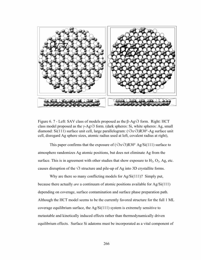
266
Figure 6. 7 - Left: SAV class of models proposed as the β-Ag√3 form. Right: HCT class model proposed as the γ-Ag√3 form. (dark spheres: Si, white spheres: Ag, small diamond: Si(111) surface unit cell, large parallelogram: (√3x√3)R30°-Ag surface unit cell, disregard Ag sphere sizes, atomic radius used at left, covalent radius at right),
This paper confirms that the exposure of (√3x√3)R30° Ag/Si(111) surface to
atmosphere randomizes Ag atomic positions, but does not eliminate Ag from the
surface. This is in agreement with other studies that show exposure to H2, O2, Ag, etc.
causes disruption of the √3 structure and pile-up of Ag into 3D crystallite forms.
Why are there so many conflicting models for Ag/Si(111)? Simply put,
because there actually are a continuum of atomic positions available for Ag/Si(111)
depending on coverage, surface contamination and surface phase preparation path.
Although the HCT model seems to be the currently favored structure for the full 1 ML
coverage equilibrium surface, the Ag/Si(111) system is extremely sensitive to
metastable and kinetically induced effects rather than thermodynamically driven
equilibrium effects. Surface Si adatoms must be incorporated as a vital component of

267
the structure. For example, a Ag-√3 structure formed at 0.25 ML on a 7x7 surface
has different atomistic details than a √3 structure formed by deposition to high
coverage and then thermally desorbed back to 0.25 ML. The former treatment
accommodates Ag into a modified DAS structure, the latter modifies the DAS
structure, especially the Si adatoms prior to taking their place as the sole gratification
for surface dangling bonds. The end point is the same, the √3 structure without careful
spot profile analysis is the same but the specific atomic arrangements of Si and Ag
look different to different probe techniques. In short, there are many paths to the same
surface projected Ag-(√3x√3)R30° structure.
This Ag/Si(111)system is complex and subtle, yet in it’s complexity lies the
potential for great utility. It is time to put that tremendous potential to use in practical
applications.