simple represbntation of the behaviour of a … bound... · simple represbntation of the behaviour...
TRANSCRIPT

SIMPLE REPRESBNTATION OF THE BEHAVIOUR OFA DIODE IN CONVERTER CIRCUITS
1. IntroduetionIn the past few years the parametrie amplifier, and recently the tunnel-diode
converter have been investigated intensively 2-6). The diode converter and thedetector had earlier been analyzed in detail. All these circuits contain a diodeas a one-port non-linear element. Other common points are the presence ofthree signals with different frequencies, one of the signals being large withrespect to the others.
Once struck by this congruence one is tempted to believe that there mustexist a general way of describing the behaviour ofthese circuits. Several attemptsin this direction have been reported in the literature 7,8) but they all suffer moreor less from a mathematical complexity, making it difficult to obtain a clearinsight into those properties of the circuit which are important to the designer.The need for such an insight is well known to those experimenting with para-metric amplifiers and tunnel-diode converter circuits.
R 461 Philips Res. Repts 17, 431-450, 1962
by L. J. V1!-Ïl de POLDER 621.372.63: 621.232.2
SummaryThe behaviour of a diode in converter circuits can be simply representedby means ofphasor diagrams. In this way a clear insight can be obtainedinto the properties of detectors, diode converters, parametrie amplifiersand tunnel-diode converters, especially with regard to input, transferand output impedances, bandwidth and amplification, without makinguse of extensive mathematical calculations. It is shown that there is alarge measure of conformity between these converter circuits.
RésuméLe comportement d'une diode dans des circuits convertisseurs peutêtre représenté simplement à l'aide de diagrammes vectoriels. On obtientainsi un excellent aperçu des propriétés présentées par les convertisseursà diode tunnel, détecteurs, mélangeurs à diode et amplificateurs para-métriques, particulièrement en ce qui concerne les impédances d'entrée,de transfert et de sortie, la largeur de bande et l'amplification, sans pourcela avoir recours à de nombreuxcalculs mathématiques. L'auteur montrequ'il existe de nombreuses similitudes entre ces circuits convertisseurs.
ZusammenfassungDas Verhalten einer Diode in Mischstufen läBt sich in Vektordiagram-men einfach darstellen. Auf diese Weise erhält man einen klaren Ein-bliek in die Eigenschaften von Detektoren, Diodenmischern, parame-trischen Verstärkern und Tunneldioden-Mischstufen, besonders hin-sichtlich der Eingangs-, Übertragungs- und Ausgangsimpedanz, Band-breite und Verstärkung, ohne daB ausgedehnte Berechnungen anzu-stellen sind. Es wird gezeigt, daB diese Mischstufen in ho hem MaBeübereinstimmen.

432 L. J. van de POLDER
In the following pages a simple explanation by means of phasor diagramswill be described without making use of many extensive mathematical calcula-tions. We shall start with a description of the general circuit.
9l7i
Fig. 1. The general converter circuit. X represents the mixer diode, the tunnel-diode or theparametrie diode.
In principle all the aforementioned circuits have the construction shown infig. 1. This circuit contains:(a) The non-linear element X (converter diode, parametrie diode or tunnel-diode).(b) The input circuit Yl, containing Li, Gl and Cl, which provides an impedancefor the input signal at the frequency Wl; VI is the voltage across Yl.(c) A second circuit, usually the output circuit, Y2, containing L2, G2 and C2,which provides an impedance for the output or idler signal at the fre-quency W2; V2 is the voltage across Y2.
(d) The oscillator voltage or pump voltage V3 of frequency W3. In convertercircuits the amplitude of V3 can normally be considered as a constant.(e) The d.c. voltage source Voo This voltage may be obtained by rectifying thevoltage V3.
(f) The input current i of frequency Wl, delivered by a current source. Therelation between the three frequencies is given by
± Wl ± W2 = W3.
The voltage across the element X is equal to the sum of the voltages VI, V2,
V3 and Voo Owing to the nonlinearity of X, mixing between these voltages willoccur. Consequently the current through X contains two components of fre-quency Wl, one directly caused by the voltage VI and a second componentcaused by the mixing of the voltages V2 and V3. In the same way the currentcomponents of frequency W2 are raised by V2 and by the mixing of VI and V3.
In converter circuits the circuit Yl can be considered as a short-circuit forall frequencies other than Wl; in the same way the circuit Y2 is a short-circuitfor all frequencies but W2. For the frequency Wl the circuit of fig. 1 then re~uces

SIMPLE REPRESENTATION OF THE BEHAVIOUR OF A DIODE 433
to that of fig. 2a. The circuit of fig. 2b represents the converter circuit for thefrequency W2. The converted currents are still flowing through X.
Figure 2 will first be employed for analyzing the diode converter.
a YtFig. 2. The equivalent converter circuit consisting of the input circuit (a) and the output (oridler) circuit (b).
2. Diode converter
It is assumed that the diode is well- biased by means of the voltages Vo
and V3 and that it has no stray capacitance. The current component of fre-quency Wl through the diode, caused by the voltage VI, can be given by aOVI,
whereas the current component of frequency W2 caused by V2 can be givenby aoV2. If VI and V2 are small compared with V3 the magnitude of ao is solelydetermined by the voltages Vo and V3, and by the curvature of the il V charac-teristic ofthe diode 1). In this respect, then, the diode represents a conductancewith magnitude ao. This behaviour of the element X enables the circuit of fig. 2to be replaced by that of fig. 3.
In this figure the current source Ï1 represents the current component of fre-quency Wl which results from the mixing of the voltages V2 and V3, and i2
represents the mixing current of the voltages VI and V3. In what follows, thecurrents hand i2 will be examined.
Let us writeVI = VI' cos WIt + VI" sin WIt,
V2= V2' cos w2t + V2" sin W2t,
V3= V3' cos w3t,
h = Is' cos WIt + Ii" sin WIt,
iz = 12' cos W2t + h" sin W2t.
(1)
(2)
The currents Ï1 and iz can be written as follows
V2V3Ï! = al -,
V3'
VIV3iz = al -.
V3'
(3)

434 L. J. van de POLDER
Fig. 3. The equivalent circuit for the diode converter. In the input circuit (a) the currentsource Ï1 represents the current caused by the mixing of the voltages V2 and 'V3, in the outputcircuit (b) ;2 represents the current caused by the mixing of the voltages VI and Va.
Thè ratio al/ V3' is independent of VI and V2 for small values of these voltages,so it can be considered as a constant. The factor al is a function of V3' and Voand of the i/V characteristic of the diode. It has the dimensions of a con-ductance 1). .
2.1. Case WI + W2 = W3
For the case WI + W2 = W3 with eqs (1) and (3) it is found that
h = tal (V2' COSwlt- V2" sin WIt),i2 = tal (VI' COSw2t- VI" sin w2t), (4)
.and with eq. (2)
h' = taIV2',/1" = -tal V2",h' = talVI' ,/2" = -tal VI".
(5)
The amplitudes of hand i2 are given by
Î1 = ta!,v2,Î2= talJÎI.
(6)
Because ofthe converter action the current h is a function of VI; so the currentsource h in fig. 3a represents an admittance for the voltage VI. Now this ad-mittance will be determined.From eqs (4) and (5) it follows that for given voltages VI and V3 the current i2
is exactly determined in amplitude and phase. This can be represented in adiagram in which the sine components are drawn horizontally and the cosinecomponents vertically, as shown in fig. 4. .This diagram shows the phase relation between VI, V3 and i2; the phase
angle cP represents the reference phase of VI. The diagram of fig. 4 and thefollowing diagrams differ from a normal diagram in so far as differentfrequenciesare represented in one figure. -Now the current i2 causes the voltage V2 across the circuit consisting of Y2

SIMPLE REPRESENTATION OF THE BEHAVIOUR OF A DIODE 435
\5v,' ----- It,
____ I~
I2 14" 9371
Fig. 4. Phasor representation of the current i2 of frequency W2, caused by' the mixing of thevoltages Vl of frequency Wl and va of frequency wa, where W2 = wa - Wl.
and ao (fig. 3b). If we consider the case where W2 is equal to the resonancefrequency .Q2 of Y2 the voltage V2 is exactly opposite in phase to iz (fig. 5).The amplitude of V2 is given by
A Î2 -! al lÎIV2=---= ,
G2+ao G2+ao
SO that the voltage-conversion factor V2/VI is equal to
-! alG2 + ao
The voltage V2 across the diode together with the voltage V3 gives rise tothe current iz as given by eqs (4) and (5) (fig. 6). The combination of figs4, 5and 6 leads to fig. 7. This shows that the given voltage VI, with frequency WI,
gives rise to a current i: with the same frequency and exactly opposite in phase.Hence in fig. 3a the current source ir can be replaced by a negative conduc-tance G-. lts magnitude follows from
(7)
(8)
The total conductance GD of the element X in fig. 3a is therefore equal to
(9)
9378
Fig. 5. Phasor representation of the voltage V2 caused by the current i2 (for W2 = Q2).

436 L. J. van de POLDER
9379
Fig. 6. Phasor representation of the current h of frequency Wl caused by the mixing of thevoltages V2 of frequency W2 and va of frequency wa.
For a normal diode this quantity is always positive.The above discussion holds for the case whenthe frequency wz is equal to
the resonance frequency .Qz of Yz, so WI = W3 - .Qz. If WI has a differentvalue one has to take into account the impedance ZZt formed by the circuitof Y2 and ao (fig. 3b). This impedance as a function of frequency is representedin fig. 8 (the arrow W gives the direction of increasing frequency).
Now the voltage V2 shows a phase shift of 7T - cPz with respect to ie, cP2beingthe phase angle of Z2t, and the amplitude of V2 is proportional to the amplitudeof Z2t.In this general situation the converter process can now be represented by
fig. 9. The phases of Ï! and Vz are symmetrical with respect to the V3-axis,and so the voltage VI ultimately gives rise to the current Ï! with a phase angle7T - cP2 in relation to VI. The amplitude of i: is proportional to ZZt. Hencethe current source h in fig. 3a represents an admittance Y_, which is shown
v,
I1 9380
Fig. 7. Combined phasor representation of the diode converter for W2 = wa- Wl = Q2. Thevoltage Vl ultimately gives rise to the current h; both have frequency Wl.

SIMPLE REPRESENTATION OF THE BEHAVIOUR OF A DIODE 437
!!. 9381
Fig. 8. The impedance diagram Cb) for the circuit Z2t consisting of Y2 and ao Ca).
in fig. 10 as a function of the input frequency. This figure shows how theimpedance Z2t is converted to a similar admittance in the input frequency band.This admittance can be replaced by the admittance of the series-resonating
circuit as indicated in fig. 11, with a resonance frequency W3 - Q2 and abandwidth equal to that of Z2t. The value of G- is given by formula (8).If the current source ÏI in fig. 3a is replaced by the admittance Y_ the equi-
valent circuit of the converter circuit becomes as shown in fig. 12. By meansof the circuit of fig. l2a the total input admittance offered by the convertercircuit, and thus the voltage VI can easily be calculated. As the amplitude of i2is equal to tal VI, the voltage V2 can be calculated by means of fig. l2b.In order to determine the voltage VI it is useful to construct the total ad-
mittance YT of the circuit of fig. l2a (fig. 13). This construction is carried outfor every frequency WI by adding the admittance y_ and the sum of the ad-mittances YI and ao, the latter sum being represented by the straight line
""Fig. 9. Phasor representation of the mixing-process for the case W2 = W3 - Wl 0/= .Q2 ••
The phase angle </>2 is equal to the phase angle of the impedance Z2t.

-.
438 L. J. van de POLDER
YI + ao. The resonance frequency of YI is Sh. The construction is given forthe case Sh = W3 - Q2. The voltage VI is given by VI = i/Y T, so that the ampli-tude characteristic for Vl follows from I/YT.
2.2. Case WI + W3 = W2
Now the case WI + W3 = W2 will be examined. From eq. (3) it then followsthat
Ï! = tal (V2' COSwIt + V2" sin wIt),i2 = tal (VI' COSw2t + VI" sin W2t),
orIs' = talV2' ,Is" = tal V2",12' = -tal VI' ,12" = tal VI".
(10)
(11)
Fig. 10. The admittance diagram for the current source ii of fig. 3a.
om
Fig. 11. Equivalent circuit for the current source h of fig. 3a.
fig. 12. The complete equivalent circuit for the diode converter.
r-~-.,I iI II 6_1I II I
I ~_!1 II 1I 1I L_I-Y_L__ J
"s<

SIMPLE REPRESENTATION OF THE BEHAVIOUR OF A DIODE 439
9386
Fig. 13. The total input admittance YT of the diode converter circuit of fig. 12a, constructedby adding the admittances Yl + ao and Y_, represented respectively by the straight lineand the circle. _.
v,
I" ~"I
I W'111 Vz-- V;III I'
i; 1
9387
Fig. 14. Phasor representation of the mixing-process for the case W2 = Wl + W3 = Q2.
It,
/'(II
9188
Fig. 15. Phasor representation of the mixing-process for the case W2 == Wl + W3 * Q2.

us,
440 L. J. van de POLDER
Fig. 16. The admittance diagram for the current source it of fig. 3a for lIJ2 = lIJ1 + lIJ3.
As in the preceding section, the current h can be determined as a functionof the given voltage VI. For the case WI = Q2 - wa this results in fig. 14. Thisfigure shows that the current h is opposite in phase to VI; so again the con-ductance represented by the current source h is a negative one. This con-ductance is again
ial2G-=- .
G2 + ao
For the case WI =1= Q2 - wa the phasor representation is given by fig. IS.The admittance diagram corresponding to the current source i: is given by
fig. 16.Since both arrows W point in the same direction, figs 16 and 10 are
identical. For the cases WI + W2 = wa and WI + wa = W2, therefore, the sameequivalent circuits (figs 11 and 12) can be used. The construction of the totaladmittance YT also gives the same result (fig. 13).
3. Tunnel-diode converter
In general ao is smaller for a tunnel diode than for a normal diode; ao caneven be negative, depending on the bias voltage Vo and the amplitude of theoscillator voltage Va (fig. I).Furthermore a current h, caused by the voltages V2 and Va, and the current i2,
caused by the voltages VI and Va, will flow, the ratio factor being again -tal.With the tunnel-diode converter al is negative, but as can be seen fromfigs 7 and 14 the resulting current h remains opposite in phase to VI. Thenegative conductance G- again amounts to
ial2G-=- ---
This shows that no great differences exist between the normal diode converterand the tunnel-diode converter; only the values of ao and al are different.The total conductance GDrepresented by the tunnel-diode is
ial2GD=ao--~-G2 + ao
This conductance can be negative, so that it ispossible to obtain amplification 5).

SIMPLE REPRESENTATION OF THE BEHAVIOUR OF A DIODE 441
4. Parametrie amplifier
4.1. Negative-resistance case WI+ W2= W3
As is well known, normally in this application a back-biased diode is usedfor the element X of fig. 1. Because of the pump-voltage V3 this diode behaveslike a time-varying capacitance.In the first place the diode represents an average capacitance Co for the
voltages VI and V2, so that the equivalent circuit of fig. 2 can be replaced bythat of fig. 17.
Fig. 17. The equivalent circuit diagram for the parametrie amplifier.
For the sake of simplicity the pump-voltage V3 can be defined by
The choice of the sine component is significant because of the followingdifferentiation. The currents hand i2 due to the mixing-process follow from
The capacitance C' is roughly proportional to V3" B). With eqs (12) and(13) one finds
C' d(VIV3)
dti2 -
V3"
(12)
(13)
h = tWIC' (V2' cos WIt- V2" sin WIt),iz = tW2C' (VI' cos w2t - VI" sin w2t),
h' = tWIC' V2' ,11" = -twIC' V2" ,12' = tW2C' VI' ,h" =-tW2C' VI" .
A comparison ofeqs (14) and (4) shows that only the coefficients are different.The phasor diagram of the parametrie amplifier is shown in fig. 18. This figureis drawn for the case WI= W3- Q2 where Q2 follows from (fig. 17b):
or
(14)
(15) ,
.._-------------------~----~------------

442 L. J. van de POLDER
:L1
Fig. 18. Phasor representation of the parametrie amplifier (negative-resistance case).
Q22L2 (C2 + Co) = 1.
The current source i] in fig. 17a represents a negative conductance G- whichfollows from
This is a well-known formula.By a reasoning analogous to that employed before it can be shown that ~he
current source h in fig. 17 can be again replaced by the series-resonant circuitof fig. 11. Hence the equivalent circuit of the parametrie amplifier becomes asgiven in fig. 19.The resonance frequency of y_ is equal to W3 - Q2, the bandwidth of y_
is equal to the bandwidth of Y2 + Co. It may be remarked that the equivalentcircuit of fig. 19a gives complete information on the behaviour of the circuitwhen the output frequency is equal to Wl.
Theconstruction ofthe total admittance YT ofthe circuit of fig. 19a is givenin fig. 20 *).
Fig. 19. The equivalent circuit of the parametrie amplifier.----:j .*) While preparing the manuscript, for the case of the parametrie amplifier the representa-
tion of y_ by means of a circle was published by Schilling 10).
SIMPLE REPRESENTATION OF THE BEHAVIOUR OF A DIODE 443
9393
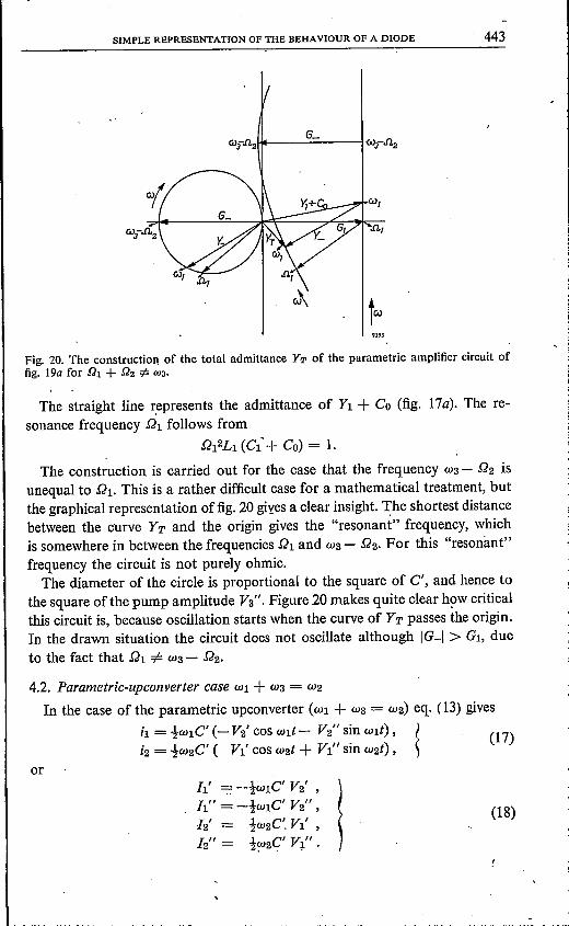
Fig. 20. The construction of the total admittance YP of the parametrie amplifier circuit offig. 19a for .QI + .Q2 =F <03.
The straight line r:epresents the admittance of Y1 + Co (fig. 17a). The re-sonance frequency Q1 follows from
Q12L1 (Cl+ Co) = 1.
The construction is carried out for the case that the frequency W3- Q2 isunequal to Q1. This is a rather difficult case for a mathematical treatment, butthe graphical representation of fig. 20 gives a clear insight. The shortest distancebetween the curve YT and the origin gives the "resonant" frequency, whichis somewhere in between the frequencies Q1 and W3 - Q2. For this "resonant"frequency the circuit is not purely ohmic.The diameter of the circle is proportional to the square of C', and hence to
the square ofthe pump amplitude V3". Figure 20 makes quite clear how criticalthis circuit is, because oscillation starts when the curve of YT passes the origin.In the drawn situation the circuit does not oscillate although IG-I > G1, dueto the fact that Q1 =1= W3 - Q2.
4.2. Parametric-upconverter case W1+ W3 = W2
In the case of the parametrie upconverter (W1 + W3 = W2) eq. (13) gives
~Ï1 = tW1C' (- V2' cos w1t- V2" sin w1t),
i2 = tW2C' ( V1' cos W2t + V1" sin w2t) ,(17)
or
T"L2 =
(18)
Is' = --tw1C' V2' ,
J1" = -!W1 C' V2" ,
[Z' = tW2C'. V1' ,

·444 L. J. van "de POLDER
It,
. ~
Fig. 21. Phasor representation of the parametrie amplifier (upconverter case).
Comparison with formula (10) shows that two signs have changed. Thephasor diagram of the upconverter is drawn in fig. 21.This figure holds for the case WI = .Q2 - wa. It shows that the current Ï! is
in phase with VI; so the current source Ï! now represents a positive conduc-tance G+, WhIChis equal to
The circuit of fig. 19 can be used for the upconverter if the negative signsof y_ are altered to positive signs.The construction of the total admittance YT of the circuit of fig. 19a is given
in fig. 22.This figure is constructed for the matched condition (G+ = GI), where
!h= .Q2 - wa and the bandwidth at WI is equal to the bandwidth at W2.
From fig. 22 we see that the amplitude characteristic of VI will show a valley,and that the bandwidth is large. The discussion above shows that of all the
Fig. 22. The construction of the total admittance YP of the parametrie upconverter circuitof fig. 19a for the case .Q2 = .Q1 + wa. '

SIMPLE REPRESENTATION OF THE BEHAVIOUR OF A DIODE 445
9396
Fig. 23. Phasor representation of a double-sideband modulated signal.
converter circuits analyzed so far, the upconverter is the only one which hasa different character.
5. Diode detector
5.1. Detection of a double-sideband signalWe shall now apply the method developed in the preceding sections to
analyzing the detection of a double-sideband signal with low modulation level.The phasor diagram of a double-sideband signal is given in fig. 23.
In this figure V3 represents the carrier voltage
V3= V3' cos w3t.Further
Vu= Vu' cos (W3+ wm)t + Vu" sin (W3+ wm)t
stands for the upper-sideband signal and
Vz= Vt' cos (W3- wm)t + VI" sin (W3- wm)t
Vu
9)97
Fig. 24. Phasor representation for the detection of a double-sideband signal.

446 L. J. van de POLDER
Fig. 25. The low-frequency part of the detector circuit for the case Wm _,. O.
for the lower-sideband signal; Wm is the modulation frequency. For an un-distorted double-sideband signal
Vu' = VI' and Vu" = VI".
The amplitudes of the two sideband signals are equal:
Vu = Vl.
If the double-sideband signal is present across the diode, the voltages Vu and Va
give rise. to the current imu of frequency Wm, while VI and Va give rise to thecurrent iml, also of frequency Wm (fig. 24). These two currents are equal andin phase.The total current im of frequency Wm is
im = imu + iml.
Let the equivalent circuit for the frequency Wm be given by fig. 25 (fig. 25corresponds to fig. 12b for the case W2 = Q2). Then the current im gives riseto the voltage Vm (fig. 24); the amplitude of Vm is given by
Îm al VuVm= = .
Gm + ao Gm + aO
Next the voltages Vm and Va give rise to the currents iu, offrequency wa + Wm,and ii, of frequency wa - Wm.
Now fig. 24 shows that for both sideband frequencies the diode circuit re-presents a negative conductance G_, which is equal to
G-=- (19)
Fig. 26. The complete low-frequency part of the detector circuit:

r-------;;-----------~--- - -----
SIMPLE REPRESENTATION OF THE BEHAVIOUR OF A DIODE 447
'<00
Fig. 27. The impedance diagram for the circuit of fig. 26.
Normally a capacitance Cm is used in parallel to the detection conduc-tance G1n (fig. 26).The circuit of fig. 26 gives rise to a phase shift 1>m (fig. 27); the impedance
of the circuit is Zm.From the foregoing it will be clear that for the input frequency band the
equivalent circuit of the detector circuit can be represented by the circuitdiagram of fig. 12a, in which G- is given byeq. (19). The resonant frequencyof Y_ is equal to W3 and. the bandwidth of y_ is twice the bandwidth of thecircuit of fig. 26. The latter figure represents the low-frequency part of theequivalent cir~uit.
5.2. Vestigial sideband reception
Next we will examine the case where the sideband amplitudes are unequal,as they are in vestigial sideband transmission. The phasor diagram belongingto the equivalent circuit of fig. 25 is depicted in fig. 28.The amplitudes of the two currents iu and it are equal, and as the amplitudes
Vu.
Fig.'28. Phasor representation for the detection of a vestigial sideband signal.
448 L. J. van de POLDER
9402
Vz
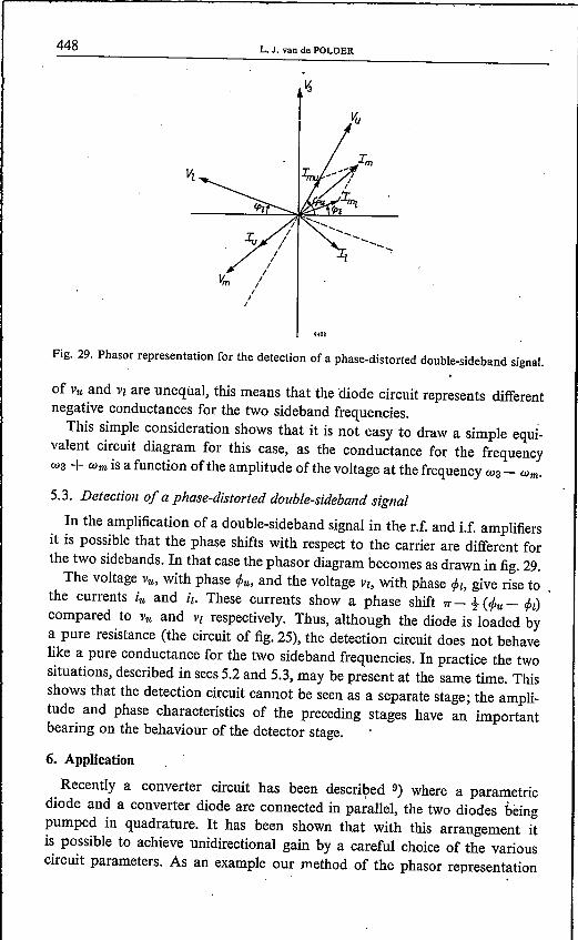
Fig. 29. Phasor representation for the detection of a phase-distorted double-sideband signal.
of Vu and Vl are unequal, this means that the diode circuit represents differentnegative conductances for the two sideband frequencies.This simple consideration shows that it is not easy to draw a simple equi-
valent circuit diagram for this case, as the conductance for the frequencyW3 + Wm is a function of the amplitude of the voltage at the frequency W3 - Wm.
5.3. Detection of a phase-distorted double-sideband signal
In the amplification of a double-sideband signal in the r.f. and i.f. amplifiersit is possible that the phase shifts with respect to the carrier are different forthe two sidebands. In that case the phasor diagram becomes as drawn in fig. 29.The voltage Vu, with phase ~u, and the voltage Vl, with phase ~l, give rise to .
the currents iu and ii. These currents show a phase shift 'TT - t (CPu - ~l)compared to Vu and Vl respectively. Thus, although the diode is loaded bya pure resistance (the circuit of fig. 25), the detection circuit does not behavelike a pure conductance for the two sideband frequencies. In practice the twosituations, described in secs 5.2 and 5.3, may be present at the same time. Thisshows that the detection circuit cannot be seen as a separate stage; the ampli-tude and phase characteristics of the preceding stages have an importantbearing on the behaviour of the detector stage.
6. Application
Recently a converter circuit has been described 9) where a parametriediode and a converter diode are connected in parallel, the two diodes beingpumped in quadrature. It has been shown that with this arrangement itis possible to achieve unidirectional gain by a careful choice of the variouscircuit parameters. As an example our method of the phasor representation

,.---------------~- ~~~~
SIMPLE REPRESENTATION OF THE BEHAVIOUR OF A DIODE 449
Fig. 30. The equivalent circuit for a converter circuit containing a converter diode Xl and aparametrie diode X2 in parallel.
will be applied to this special case. The equivalent circuit is given in fig. 30,where Xl represents the converter diode and X2 stands for the parametrie diode.In the case Wl + wa = W2 the phasor representation of fig. 14 holds for Xl,
whereas for X2 the diagram of fig. 21 is valid. The current at the output stageis now given by
i2G + i2C = G~al+ tW2C') VI,
and the sum of the currents is.a and iio at the input stage is given by
iia + i10 = (tal- -tWlC') V2·
The latter current is equal to zero for any value of V2 if
In that case, therefore, the down-conversion gain is zero and no feedback ispresent. The forward current becomes
i2G + i2C = tal (1 + W2!Wl) Vl·
The equivalent circuit of fig. 30 now reduces to that of fig. 31, from whichit can be seen that input matching occurs for Gl = 0.0 and output matchingfor G2 = o.o.
Fig. 31: The equivalent circuit for a converter circuit containing a converter diode and aparametrie diode in parallel for the case al = wIG';
i2G + i2C = tal (1 + W2/WI) VI if Wl + W3 = W2,
i2G + i2C = tal (1 - W2/wl) VI ~if Wl + W2 = W3·
s b 9,,03

450 L. J. van de POLDER
With the aid of the phasor representations in figs 7 and 18 it is found thatthe same result can be obtained for the case WI + W2 = W3 by choosingal = WIC', provided that at the same time the phase of the pump voltage ofone of the two diodes is shifted over 180°. The forward current is then
i2G + i20 = (tal - -!W2C') VI = tal(1 - W2/WI) Vl.
By means of the equivalent circuit diagrams other properties can readily be,determined.
7. Final Remarks
In the preceding sections the input admittances of the investigated convertercircuits are determined; the output admittances may be found in an identicalway.For the admittance YI it is assumed that it is a short-circuit for all frequencies
other than WI. If on the contrary it has a finite impedance for the frequency W2
then the total impedance Z2t of fig. 8a will alter a little; the admittance YI isin series with Y2. This means that the impedance diagram of fig. 8b wiIl not bea pure circle.As a result of the mixing-process this new impedance is converted into a'
similar admittance in the input frequency band.If the diode contains a series resistance, the equivalent-circuit diagrams must
be extended. In the case of the parametrie amplifie.r this can be carried out infigs 17a and 17b by adding a resistor in series 'with the element X. The sameholds for the diode converter circuit (figs 3a and 3b) but in this case it is alsopossible to alter the values of ao and al.
Acknowledgement
The author is indebted to G. J. Lubben for critically reading the manuscript.
Eindhoven, August 1962
REFERENCES1) J. Haantjes and B. D. H. Tellegen, Philips Res. Repts 2, 401-419, 1947.2) H. Heffner and G. Wade, J. appl. Phys. 29, 1321-1331,1958.3) S. Bloom and K. K. N. Chang. R. C. A. Rev. 18, 578-593, 1957.4) W. Dahlke, R. Maurer und J. Schu bert, Arch. e1ektr. Übertr. 13, 321-340, 1959.5) K. K. N. Ch ang, G. H. Heilmeier and H. J. Prager, Proc. Inst. Radio Engrs 48,
854-858, 1960.6) K. Wohlberg, Te1efunken Zeitung34, 114-121, 1961.7) K: H. Steiner, Arch. elektro Übertr. 14, 482-486, 1960.8) K. H. Steiner, Arch. elektro Übertr. 16, 67-82. 1962,9) R. S. Engelbrecht, Proc. Inst. Radio Engrs 50,312-321, 1962.la) G. Schilling, Frequenz 16, 171-176, 1962. .