skp engineering college -...
TRANSCRIPT

S.K.P. Engineering College, Tiruvannamalai IV SEM
Electronics and Communication Engineering Department 1 Linear Integrated Circuits
SKP Engineering College Tiruvannamalai – 606611
A Course Material
on Linear Integrated Circuits
By
A.Vigneswaran
Assistant Professor
Electronics and Communication Engineering Department

S.K.P. Engineering College, Tiruvannamalai IV SEM
Electronics and Communication Engineering Department 2 Linear Integrated Circuits
Quality Certificate
This is to Certify that the Electronic Study Material
Subject Code: EC6404
Subject Name: Linear Integrated Circuits
Year/Sem: II /IV
Being prepared by me and it meets the knowledge requirement of the University curriculum.
Signature of the Author
Name: A.Vigneswaran
Designation: Assistant Professor
This is to certify that the course material being prepared by Mr.A.Vigneswaran is of the adequate quality. He has referred more than five books and one among them is from abroad author.
Signature of HD Signature of the Principal
Name: Name: Dr.V.Subramania Bharathi
Seal: Seal:

S.K.P. Engineering College, Tiruvannamalai IV SEM
Electronics and Communication Engineering Department 3 Linear Integrated Circuits
EC6404 LINEAR INTEGRATED CIRCUITS L T P C 3 0 0 3
OBJECTIVES: To introduce the ba s ic building blocks of line a r inte gra te d circuits .
To le a rn the line a r a nd non-linear applications of operational amplifiers.
To introduce the the ory a nd a pplica tions of a na log multiplie rs a nd P LL.
To le a rn the the ory of ADC a nd DAC.
To introduce the conce pts of wa ve form ge ne ra tion a nd introduce s ome s pe cia l
function ICs.
UNIT I BASICS OF OPERATIONAL AMPLIFIERS 9 Current mirror and current sources, Current sources as active loads, Voltage sources,
Voltage References, BJT Differential amplifier with active loads, Basic information about
op-amps – Ideal Operational Amplifier - General operational amplifier stages -and
internal circuit diagrams of IC 741,DC and AC performance characteristics, slew rate,
Open and closed loop configurations.
UNIT II APPLICATIONS OF OPERATIONAL AMPLIFIERS 9 Sign Changer, Scale Changer, Phase Shift Circuits, Voltage Follower, V-to-I and I-to-V
converters,adder, subtractor, Instrumentation amplifier, Integrator, Differentiator,
Logarithmic amplifier,Antilogarithmic amplifier, Comparators, Schmitt trigger, Precision
rectifier, peak detector, clipper and clamper, Low-pass, high-pass and band-pass
Butterworth filters.
UNIT III ANALOG MULTIPLIER AND PLL 9 Analog Multiplier using Emitter Coupled Transistor Pair - Gilbert Multiplier cell – Variable
transconductance technique, analog multiplier ICs and their applications, Operation of
the basic PLL, Closed loop analysis, Voltage controlled oscillator, Monolithic PLL IC
565, application of PLL for AM detection, FM detection, FSK modulation and
demodulation and Frequency synthesizing.

S.K.P. Engineering College, Tiruvannamalai IV SEM
Electronics and Communication Engineering Department 4 Linear Integrated Circuits
UNIT IV ANALOG TO DIGITAL AND DIGITAL TO ANALOG CONVERTERS 9 Analog and Digital Data Conversions, D/A converter – specifications - weighted resistor
type, R-2R Ladder type, Voltage Mode and Current-Mode R 2R Ladder types -
switches for D/A converters,high speed sample-and-hold circuits, A/D Converters –
specifications - Flash type – Successive Approximation type - Single Slope type – Dual
Slope type - A/D Converter using Voltage-to-Time Conversion - Over-sampling A/D
Converters.
UNIT V WAVEFORM GENERATORS AND SPECIAL FUNCTION ICS 9 Sine-wave generators, Multivibrators and Triangular wave generator, Saw-tooth wave
generator,ICL8038 function generator, Timer IC 555, IC Voltage regulators – Three
terminal fixed and adjustable voltage regulators - IC 723 general purpose regulator -
Monolithic switching regulator, Switched capacitor filter IC MF10, Frequency to Voltage
and Voltage to Frequency converters, Audio Power amplifier, Video Amplifier, Isolation
Amplifier, Opto-couplers and fibre optic IC.
TOTAL: 45 PERIODS OUTCOMES: Upon Completion of the course, the students will be able to: De s ign line a r a nd non line a r a pplica tions of op – amps.
Design applications using analog multiplier and PLL.
De s ign ADC a nd DAC using op – amps.
Generate waveforms using op – amp circuits.
Analyze special function ICs.

S.K.P. Engineering College, Tiruvannamalai IV SEM
Electronics and Communication Engineering Department 5 Linear Integrated Circuits
CONTENTS
S.No Particulars Page
1 Unit – I 6
2 Unit – II 26
3 Unit – III 77
4 Unit – IV 99
5 Unit – V 132

S.K.P. Engineering College, Tiruvannamalai IV SEM
Electronics and Communication Engineering Department 6 Linear Integrated Circuits
Unit – I
Basics Of Operational Amplifiers
Part – A
1. A differential amplifier has a differential voltage gain of 2000 and a common
mode gain of 0.2. Determine the CMRR in dB. [CO1-H1-April/May 2015]
CMRR =
CMRRdB = 20 log
1010000 = 80dB
2. Define Slew rate and what causes slew rate? [CO1-L1-April/May 2015] Slew rate is defined as the maximum rate of change of output voltage realized
by a step input voltage and it is usually specified in units of V/µs. The slew rate of
the op-amp is related to its frequency response.
Causes of Slew rate: The slew rate is determined by a number of factors such as the amplifier gain,
compensating capacitors and the change in polarity of output voltage. It is also a
function of temperature and the slew rate generally reduced due to rise in
temperature.
3. Mention two advantages of active load over passive load in an operational amplifier.[CO1-L1-Nov/Dec 2015] To achieve high voltage gain without requiring large power supply voltage active
load is used in an operational amplifier.
4. Define input bias current and input offset current of an operational amplifier. [CO1-L1-Nov/Dec 2015]

S.K.P. Engineering College, Tiruvannamalai IV SEM
Electronics and Communication Engineering Department 7 Linear Integrated Circuits
Input Bias Current : The average of the currents entering into the (-) input and
(+) input terminals of an op-amp is called input bias current. Its value is 500nA for
741C.
Input Offset Current : The algebraic difference between the currents into the (-)
input and (+) input is referred to as the input offset current. It is 200nA maximum
for 741C.
5. Find the maximum frequency for sine wave output voltage 10 V peak to peak with an op-amp whose slew rate is 1 V/µS. [CO1-H1-April/May 2016] To find maximum frequency : fmax = Slew rate / 2πm
= 1V/µs / 2π x 10
6. Define CMRR of an op-amp. [CO1-L1] CMRR is defined as the ratio of the differential voltage gain to common mode
voltage gain. It is expressed in decibels. CMRR= Ad/Ac
7. Differentiate the ideal and practical characteristics of an op-amp. [CO1-H1-May/June 2016] Ideal Characteristics Open loop voltage gain, AOL = ∞
Input impedance, Ri = ∞
Output impedance,Ro = 0
Bandwidth, BW = ∞
Zero offset, i.e. Vo = 0 when V1 = V2 = 0
Practical Characteristics Open loop voltage gain, AOL ≠ Infinity
Input impedance, Ri ≠ Infinity
Output impedance, Ro ≠ 0
8. Draw the block diagram of a general opamp. [CO1-L1-Nov/Dec 2016]

S.K.P. Engineering College, Tiruvannamalai IV SEM
Electronics and Communication Engineering Department 8 Linear Integrated Circuits
9. Draw the circuit diagram of a symmetrical emitter coupled differential
amplifier. [CO1-L1- Nov/Dec 2016]
10. State the advantages of IC over discrete components [CO1-L1]
Miniature in size and hence increased equipment density
Improved performance
Low cost due to batch processing
High reliability and ruggedness
Low power consumption
Less vulnerability to parameter variations
Increased operating speeds
11. Define Unity gain bandwidth of an op-amp. [CO1-L1]

S.K.P. Engineering College, Tiruvannamalai IV SEM
Electronics and Communication Engineering Department 9 Linear Integrated Circuits
The unity gain bandwidth is the bandwidth of the op-amp when the voltage gain
is unity. The other terms are Closed-loop bandwidth, Gain-bandwidth product
and Small-signal bandwidth.
For general purpose op-amps, the gain-bandwidth product is in the range of 1 to
20 MHz.For an op-amp with a single break frequency f1 ,the gain-bandwidth
product is constant and it can be written as Unity Gain Bandwidth UGB = Ao f1
12. Mention the characteristics of an operational-amplifier. [CO1-L1] a.c characteristics d.c characteristics
i) Frequency response i) Input bias current ii) Bandwidth ii) Input offset current iii) Slew rate. iii) Input offset voltage iv) Thermal drift
13. What are the applications of current sources? [CO1-L3] Transistor current sources are widely used in analog ICs both as biasing elements
and as load devices for amplifier stages.
14. Justify the reasons for using current sources in integrated circuits. [CO1-H2] Superior insensitivity of circuit performance to power supply variations and
temperature.
More economical than resistors in terms of die area required providing bias currents
of small value.
•When used as load element, the high incremental resistances of current source
results in high voltage gain at low supply voltages.
15. Why current mirror is used as a active load? [CO1-L1] A Current mirror can be used as an active load because it has high ac resistance.
16. Explain the meaning of open loop and closed loop operation of an op-amp. [CO1-L1] In open loop mode, the output of the op-amp is at positive or negative saturation
level. It does not operate linearly in this mode.

S.K.P. Engineering College, Tiruvannamalai IV SEM
Electronics and Communication Engineering Department 10 Linear Integrated Circuits
17. What is a practical op-amp? Draw its equivalent circuit. [CO1-L1]
18. What is a current mirror and why it is called so? [CO1-L2] A current mirror is a circuit block which functions to produce a copy of the current
in one active device by replicating the current in second active device. An important
feature of the current mirror is a relatively high output resistance which helps to keep
the output current constant regardless of load conditions. Another feature of the
current mirror is a relatively low input resistance which helps to keep the input
current constant regardless of drive conditions. The current being 'copied' can be,
and often is, a varying signal current.
19. Define virtual ground property of Op-amp. [CO1-L1] Concept of virtual ground says that the two input terminals of the Op-amp are always
at potential. Thus if one terminal is grounded the other can be assumed to be at
ground potential, which is called virtual ground.
20. What are the frequency compensation techniques used in practice? [CO1-L3]
Two methods of compensation techniques are used in practice :
(1) External frequency compensation
(2) Internal frequency compensation

S.K.P. Engineering College, Tiruvannamalai IV SEM
Electronics and Communication Engineering Department 11 Linear Integrated Circuits
The commonly used external compensation methods are :
(i) Dominant-pole compensation (ii) Pole-zero(lag) compensation
Part B
1. Explain the significance of virtual ground in an opamp. [CO1-L1-Nov/Dec 2016] The concept of a virtual ground is based on an ideal op-amp. When an op-amp is ideal, it has infinite open-loop voltage gain and infinite input resistance. Because of this, we can deduce the following ideal properties for the inverting amplifier : (1) Since Rin is infinite, i2 is zero. (2) Since AOL is infinite, V2 is zero.
The Virtual ground shown in the figure means that the inverting input acts like a ground for voltage but an open for current. Virtual ground is very unusual. It is like half of a ground because it is a short for voltage but an open for current . In the figure, dashed line is shown between the inverting input and ground. The dashed line means that no current can flow to ground. Although virtual ground is an ideal approximation, it gives very accurate answers when used with very heavy negative feedback.
2. Explain the operation of a current mirror circuit. [CO1- L1-Nov/Dec 2016] A current mirror is a circuit block which functions to produce a copy of the current
in one active device by replicating the current in second active device. An
important feature of the current mirror is a relatively high output resistance which
helps to keep the output current constant regardless of load conditions. Another
feature of the current mirror is a relatively low input resistance which helps to

S.K.P. Engineering College, Tiruvannamalai IV SEM
Electronics and Communication Engineering Department 12 Linear Integrated Circuits
keep the input current constant regardless of drive conditions. The current being
'copied' can be, and often is, a varying signal current.
Fig. Basic Current Mirror circuit
Features Generate an output current equal to input current multiplied by desired current gain
factor
Current gain is independent of input frequency.
Output current independent of output voltage to common node.
Provide bias current to circuits like differential amplifiers, transconductance amplifiers.
Takes advantage of matching transistors on a chip.
Operation The figure shows the simplest form of current mirror circuit. Here, the transistors Q1 and
Q2 are assumed identical. VBE 1 = VBE 2
The transistor Q1 is diode connected transistor, with its collector shorted to base, such
that VCB = 0. Q1 is operating in the active region.
Since the voltages VBE1 and VBE2 are equal, Q2 will also be in the active region and the
collector currents IC1 and IC2 are equal.

S.K.P. Engineering College, Tiruvannamalai IV SEM
Electronics and Communication Engineering Department 13 Linear Integrated Circuits
Hence , this circuit is a current mirror.i.e., the current flowing through the left part of the
circuit produces a mirror image of current in the right side. This principle forms the basis
of most of the current source circuits and the active loads using current source circuits.
3. Draw the circuit of basic current mirror and explain its operation. Also discuss about, how current ratio can be improved in the basic current mirror. Sketch the improved circuit and explain. [CO1-L3]
Fig. The basic BJT current mirror
Fig.Basic Current Mirror circuit
A constant current source makes use of the fact that for a transistor in the active mode
of operation, the collector current is relatively independent of the collector voltage. In
the basic circuit shown in Fig. transistors Q1 and Q2 are matched as the circuit is
fabricated using IC technology. It may be noted that bases and emitter of Q1 and Q2
are tied together and thus have the same VBE. In addition, tran-sistor Q1 is connected
as a diode by shorting its collector to base.
The input current Iref flows through the diode-connected transistor Q1 and thus
establishes a voltage across Q1. This voltage in turn appears between the base and
emitter of Q2. Since Q2 is identical to Q1, the emitter current of Q2 will be equal to
emitter current of Q1 which is approximately equal to Iref. Thus, we can say that as

S.K.P. Engineering College, Tiruvannamalai IV SEM
Electronics and Communication Engineering Department 14 Linear Integrated Circuits
long as Q2 is maintained in the active region, its collector current Ic2 = Io will be
approximately equal to Iref. Since the output current Io is a reflection or mirror of the
reference current Iref, the circuit is often referred to as a current mirror.
This minor effect is however, valid only for large values of β.. To study the effect of β
on the operation of the current mirror circuit, we analyze it further.
Analysis The collector currents in and k2 for transistors Q1 and Q2 can be approximately
expressed as
Ic1 = αFIES eVBE1 /VT -------------------------- (1.1)
Ic1 = αFIES eVBE2 /VT -------------------------- (1.2)
From equations (1.1) and (1.2), we may write
------------------------- (1.3)
since
VBE1 = VBE2, we obtain
Ic2 = Ic1 = Io
Also since both the transistors are identical, β1 = β2 = β
KCL at the collector of Q1, gives
Iref = Ic1 + Ic2 + IB2 ------------------------------------- (1.4)
= -------------------------- (1.5)
Solving Equn (1.5), Ic may be expressed as
Ic = -------------------------------------------- (1.6)

S.K.P. Engineering College, Tiruvannamalai IV SEM
Electronics and Communication Engineering Department 15 Linear Integrated Circuits
Where Iref from figure can be seen to be
Iref = = (as VBE = 0.7 is small) --------------- (1.7)
From equation (1.6), for β >>1, β/(β+2) is almost unity and the output current Io is equal to the reference current, Iref which for a given R1 is constant. Typically Io varies by about
3 % for 50 ≤ β≤200.
Fig. Volt-ampere characterisitcs for transistor Q2
Improved Current Mirror However if β is small, then I2 cannot be equal to IC3. In such case modified current
mirror circuit is used. The improved curren mirrot circuit is shown in Fig.
Fig.Improved Current Mirror Circuit

S.K.P. Engineering College, Tiruvannamalai IV SEM
Electronics and Communication Engineering Department 16 Linear Integrated Circuits
Analysis Applying KCL at node ‘n’, we get,
I1 = IC1 + IB3
The two transistors Q1 and Q2 are identical
IB1 = IB2 = IB
Hence the emitter current IE3 of transistor Q3 gets divided equally.
Therefore, IE3 = 2IB
Now, IE3 = (1+β) IB3
2IB = (1+β) IB3
Now IC1 = IE1 = βIB
and IC2 = IE2 = βIB
Substituting,
And

S.K.P. Engineering College, Tiruvannamalai IV SEM
Electronics and Communication Engineering Department 17 Linear Integrated Circuits
4. Briefly explain about constant current source. [CO1-L1-April/May 2015] A constant current source makes use of the fact that for a transistor in the active
mode of operation, the collector current is relatively independent of the collector
voltage. In the basic circuit shown in figure transistors Q1 and Q2 are matched as
the circuit is fabricated using IC technology. It may be noted that bases and emitter
of Q1 and Q2 are tied together and thus have the same VBE. In addition, tran-sistor
Q1 is connected as a diode by shorting its collector to base. The input current /rtf
flows through the diode-connected transistor Q1 and thus establishes a voltage
across Q1. This voltage in turn appears between the base and emitter of Q2. Since
Q2 is identical to Q1, the emitter current of Q2 will be equal to emitter current of Q1
which is approximately equal to Iref. Thus, we can say that as long as Q2 is
maintained in the active region, ita collector current Ic2 = Io will be approximately
equal to Iref. Since the output current Io is a reflection or mirror of the reference
current Iref, the circuit is often referred to as a current mirror.
5. With a schematic diagram, explain the effect of RE on CMRR in differential amplifier. [CO1-H1-May/June 2016] To improve the CMRR, the common mode gain A c must be reduced. The common
mode gain A c approaches zero as RE tends to infinity. This is because RE introduces
a negative feedback in the common mode operation which reduces the common mode
gain A c. Thus higher the value of RE, lesser is the value of A c and higher is the value
of CMRR. The differential gain Ad is not dependent on RE. But practically RE can not
be selected very high due to certain limitations such as,
1. Large RE needs higher biasing voltage to set the operating Q point of the
transistors.
2. This increases the overall chip area. Hence practically instead of increasing RE
various other methods are used which provide effect of increased RE without any

S.K.P. Engineering College, Tiruvannamalai IV SEM
Electronics and Communication Engineering Department 18 Linear Integrated Circuits
limitations. Such two methods are -1. Constant current bias method. 2. Use of current
minor circuit.
The other method used to increase Ad to improve CMRR is called use of an active
load.
6. Explain with a circuit diagram, the working of BJT-emitter coupled differential amplifier, also explain the concept of Active load and sketch the relevant circuit diagram. [CO1-L2] The main purpose of the difference amplifier stage is to provide high gain to the
difference-mode signal and cancel the common-mode signal. The relative sensitivity of
an op-amp to a difference signal as compared to common-mode signal is called
common-mode rejection ratio (CMRR) and gives the figure of merit of the differential
amplifier. The higher the value of CMRR, better is the op-amp. Another requisite of a
good op-amp is that it should have high input impedance. A cascaded dc amplifier can
provide high gain down to zero fre-quency as it has no coupling capacitor. However,
such an amplifier suffers from the major problem of drift of the operating point due to
temperature dependency of /am. Vu and hn of the transistor. This problem can be
eliminated by using a balanced or differential ampli-fier as shown in Fig. .
It may be seen that it is essentialy an emitter-coupled differential amplifier. This
circuit has low drift on account of symmetrical construction. It can be designed to give
high input resistance. It has two input terminals and it may be seen easily that terminal
B2 is the inverting input terminal since transistor Q2 provides a phase shift of 180° for
the output taken at the collector of Q2. Obviously, B1 is the non-inverting input
terminal.. A differential amplifier of the type shown in Fig. can be used in four different
configurations depending upon the number of input signals used and the way output is
taken. These four configurations are:
(i) Differential-input, differential-output or Dual-input balanced-output (ii)
Differential-input, single ended-output (iii) Single-input, differential•output (iv) Single-

S.K.P. Engineering College, Tiruvannamalai IV SEM
Electronics and Communication Engineering Department 19 Linear Integrated Circuits
input, single ended-output If signal is applied to both the inputs, then it is differential
input or Dual input and the difference of signals applied to the two inputs gets
amplified. In many applications a single input is only used as we shall see later.
Similarly, if output voltage is measured between two collectors then it is a differential
output. This is also referred to as a balanced output, as both collectors are at the same
d.c. potential w.r.t. ground.
Fig. Basic differential amplifier

S.K.P. Engineering College, Tiruvannamalai IV SEM
Electronics and Communication Engineering Department 20 Linear Integrated Circuits
Fig. Differential pair with common mode input signal VCM
Fig. Differential pair with ‘large’ different input signal
7. Define CMRR. Draw the circuit of an Op-amp differential amplifier and give the expression for CMRR. [CO1- L1] The Common Mode Rejection Ratio (CMRR) is defined as the ratio of the differential
voltage gain Adm to common voltage gain Acm and is generally expressed in decibels.

S.K.P. Engineering College, Tiruvannamalai IV SEM
Electronics and Communication Engineering Department 21 Linear Integrated Circuits
8. Compare the features of ideal and practical opamp circuit. [CO1-H1- Nov/Dec 2016]
Ideal Op-amp Characteristics
Practical Op-amp Characteristics
Open loop voltage gain, AOL = ∞
Open loop voltage gain, AOL ≠ Infinity
Input impedance, Ri = ∞
Input impedance, Ri ≠ Infinity
Output impedance,Ro = 0
Output impedance, Ro ≠ 0
Bandwidth, BW = ∞
Zero offset, i.e. Vo = 0 when V1 = V2 = 0
9.With a neat block diagram, explain the general stages of an OP-AMP IC. [CO1-L1]
Fig. Internal block schematic of op-amp
Input stage The input stage requires high input impedance to avoid loading on the sources. It
requires two input terminals. It also requires low output impedance. All such
requirements are achieved by using the dual input, balanced output differential amplifier
as the input stage. The function of a differential amplifier is to amplify the difference

S.K.P. Engineering College, Tiruvannamalai IV SEM
Electronics and Communication Engineering Department 22 Linear Integrated Circuits
between the two input signals. The differential amplifier has high input impedance. This
stage provides must of the voltage gain of the amplifier.
Intermediate Stage
The output of the input stage drives the next stage which is an intermediate stage.
This is another differential amplifier with dual input, unbalanced i.e. single ended
output. The overall gian requirement of the op-amp is very high. The input stage alone
cannot provide such a high gain. The main function of the intermediate stage is to
provide an additional voltage gain required. Practically, the intermediate stage is not a
single amplifier but the chain of cascaded amplifiers called multistage amplifiers.
Level Shifting Stage
All the stages are directly coupled to each other. As the op-amp amplifies d.c. signals
also, the coupling capacitors are not used to cascade the stages. Hence the d.c.
quiescent voltage level of previous stage gets applied as the input to the net stage.
Hence stage by stage d.c. level increases well above ground potential. Such a high
d.c. voltage level may drive the transistors into saturation. This further may cause
distortion in the output due to clipping. This may limit the maximum a.c. output voltage
swing without any distortion. Hence before the output stage, it is necessary co bring
such a high d.c. voltage level to zero volts with respect to ground.
The level shifter stage brings the d.c. level down to ground potential, when no signal is
applied at the input terminals. Then the signal is given to the last stage which is the
output stage. The buffet: is usually an emitter follower whose input impedance is very
high. This prevents loading of the high gain stage.
Output Stage
The basic requirements of an output stage are low output impedance, large a.c. output
voltage swing and high current sourcing and sinking capability. The push-pull
complementary amplifier meets all these requirements and hence used as an output

S.K.P. Engineering College, Tiruvannamalai IV SEM
Electronics and Communication Engineering Department 23 Linear Integrated Circuits
stage. This stage increases the output voltage swing and keeps the voltage swing
symmetrical with respect to ground. The stage raises the current supplying capability of
the op-amp. In short, the overall block diagram can be shown as in the Fig below.
10. Assuming a slew rate for 741 IC is 0.5 v/µs. What is the maximum undistorted sinewave that can be obtained for 12 V peak. [CO1-H3-Nov/Dec 2016] Solution :
The given slew rate for 741 is 0.5 v/µs.
For the sine wave of 12V peak,
Fmax = Slew rate / 2πVm
= 0.5 v/µs / 2π x 12 V
= 6.63 kHz
11. What is the need for frequency compensation in an OPAMP? Briefly explain the techniques used for frequency compensation. [CO1-L3-April/May 2015] Concept of frequency compensation : In applications where one desires large
bandwidth and lower closed loop gain suitable compensation techniques are used.
Two used compensation techniques are used : External compensation and Internal
compensation.

S.K.P. Engineering College, Tiruvannamalai IV SEM
Electronics and Communication Engineering Department 24 Linear Integrated Circuits
External frequency compensation : Two methods are used in external compensation.
They are : Dominant pole compensation and Pole-zero (lag) compensation.
Dominant pole compensation : The dominant pole means the pole with magnitude
much smaller than the existing poles. And hence the break frequency of the
compensating network is the smallest compared to the existing frequencies.
Fig. Dominant pole compensation

S.K.P. Engineering College, Tiruvannamalai IV SEM
Electronics and Communication Engineering Department 25 Linear Integrated Circuits
It can be observed from the plot that 3 dB down bandwidth for noncompensated
system is BW1 while for compensated it becomes BW2. There is drastic reduction in
the bandwidth.
Advantages : i) As the noise frequency components are outside the smaller
bandwidth, the noise immunity of the system improves. ii) Adjusting value of fd,
adequate phase margin and the stability of the system is assured.
Disadvantage : i) The only disadvantage of the method is that the bandwidth reduces
drastically.
Pole zero compensation
In this method the transfer function A is modified by adding a pole and a zero with the
help of compensating network. The zero is added at higher frequency and the pole is
added at a lower frequency.

S.K.P. Engineering College, Tiruvannamalai IV SEM
Electronics and Communication Engineering Department 26 Linear Integrated Circuits
Fig.Pole zero compensation.
12.How do the open loop gain and the closed loop gain of an op-amp differ? [CO1-L2-April/May 2015]
Open loop configuration
Open loop gain of op-amp is very large, very small input voltage drives the op-amp voltage to the saturation level. Thus in open loop configuration, the output is at its positive saturation voltage (+Vsat) or negative saturation voltage (—Vsat) depending on which input Vt, or V2 is more than the other. For a.c. input voltages, output may switch between positive and negative saturation voltages. The Fig. shows the voltage transfer curve which indicates that in open loop mode, the input range of op-amp is very very small in AV or mV, for which op-amp behaves linearly. This range is indicated as a-b in the Fig.
Closed Loop Operation of Op-amp : The op-amp cannot operate linearity in open loop mode. But the utility of an op-amp can be considerably increased by operating it in closed loop mode. The closed loop operation is possible with the help of feedback. The feedback allows to feed some part of the output back to the input terminals. In the linear applications, the op-amp is always used with negative feedback. The negative feedback helps in controlling gain.

S.K.P. Engineering College, Tiruvannamalai IV SEM
Electronics and Communication Engineering Department 27 Linear Integrated Circuits
Fig. Op-amp with negative feedback
The advantages of negative feedback are :
i) It reduces the gain and makes it controllable. ii) It reduces the possibility of distortion. iii) It increases the bandwidth i.e. frequency range. iv) It increases the input resistance of the op-amp. v) It decreases the output resistance of the op-amp. vi) It reduces the effects of temperature, power supply on the gain of the circuit. The countless simple circuits using one or more op-amps can be designed with the help of negative feedback. Such op-amp applications are classified as linear and nonlinear type. In linear applications, output voltage varies linearily with respect to the input voltage. Some of the linear applications are inverting amplifier, noninverting amplifier, voltage follower, summing amplifier, difference amplifier etc. The concept of virtual ground plays an important role in analysing the various application circuits.

S.K.P. Engineering College, Tiruvannamalai IV SEM
Electronics and Communication Engineering Department 28 Linear Integrated Circuits
Unit - II
Applications of Operational Amplifiers
Part A
1. What is hysteresis and mention the purpose of hysteresis in a comparator? [CO2-L1-April/May 2015] The regenerative comparator or Schmitt trigger exhibits hysteresis, a deadband
condition. It means, when the input of the circuit exceeds Vut (upper threshold), Vo
switches from + Vsat to -Vsat and comeback to original state + Vsat when the input
reaches Vit (Lower threshold). The hysteresis voltage is equal to the difference
between upper threshold voltage and lower threshold voltage.
2. What is the difference between normal rectifier and precision rectifier? [CO2-L1-April/May 2015] In a normal rectifier ordinary diodes are used for rectification purpose which offers
cut-in voltage at higher order range whereas in the case of precision rectifier
precision diodes are used for rectification purpose in order to operate them for cut-in
voltages in the order of micro volts.
3. Draw the circuit diagram of a comparator. Mention its applications. [CO-L2-May/June 2016]

S.K.P. Engineering College, Tiruvannamalai IV SEM
Electronics and Communication Engineering Department 29 Linear Integrated Circuits
Applications of Comparator
Zero crossing detector
Window detector
Phase detector
Timing marker generator
4. Draw the circuit diagram of a peak detector with waveforms. . [CO2—H1-Nov/Dec2016]
5. Mention some of the linear applications of op – amps. [CO2-L1] Adder, subtractor, voltage –to- current converter, current –to- voltage
converters,instrumentation amplifier, analog computation, power amplifier, etc are some
of the linear opampcircuits.

S.K.P. Engineering College, Tiruvannamalai IV SEM
Electronics and Communication Engineering Department 30 Linear Integrated Circuits
6. Mention some of the non – linear applications of op-amps.[CO2—H1-Nov/Dec2016] Rectifier, peak detector, clipper, clamper, sample and hold circuit, log amplifier, anti –
logamplifier, multiplier are some of the non – linear op-amp circuits.
7.What is the need for an instrumentation amplifier? [CO2-L1] In a number of industrial and consumer applications, the measurement of
physicalquantities is usually done with the help of transducers. The output of transducer
has to beamplified So that it can drive the indicator or display system. This function is
performed by aninstrumentation amplifier.
8 List the features of instrumentation amplifier. [CO2-L1] • High gain accuracy
• High CMRR
• High gain stability with low temperature co-efficient
• Low dc offset
• Low output impedance
9. What are the applications of V-I converter? [CO2-L1] • Low voltage dc and ac voltmeter
• L E D
• Zener diode tester
10. What do you mean by a precision diode? [CO2-L1] The major limitation of ordinary diode is that it cannot rectify voltages below the cut –
involtage of the diode. A circuit designed by placing a diode in the feedback loop of an

S.K.P. Engineering College, Tiruvannamalai IV SEM
Electronics and Communication Engineering Department 31 Linear Integrated Circuits
op – ampis called the precision diode and it is capable of rectifying input signals of the
order of millivolt.
11. Write down the applications of precision diode. [CO2-L2] • Half - wave rectifier
• Full - Wave rectifier
• Peak – value detector
• Clipper
• Clamper
12.List the applications of Log amplifiers. [CO2-L2] • Analog computation may require functions such as lnx, log x, sin hx etc. These
functionscan be performed by log amplifiers
• Log amplifier can perform direct dB display on digital voltmeter and spectrum analyzer
• Log amplifier can be used to compress the dynamic range of a signal
13. What are the limitations of the basic differentiator circuit? [CO2-L2] At high frequency, a differentiator may become unstable and break into oscillationsThe
input impedance decreases with increase in frequency, thereby making the circuit
sensitiveto high frequency noise.
14 Write down the condition for good differentiation. [CO2-L2] For good differentiation,the time period of the input signal must be greater than or equal
to Rf C1
T > R f C1
Where, Rf is the feedback resistance Cf is the input capacitance

S.K.P. Engineering College, Tiruvannamalai IV SEM
Electronics and Communication Engineering Department 32 Linear Integrated Circuits
15.What is a comparator? [CO2-L2] A comparator is a circuit which compares a signal voltage applied at one input of an op-
ampwith a known reference voltage at the other input. It is an open loop op - amp with
output +Vsat
16.What are the applications of comparator? [CO2-L2] • Zero crossing detectors
• Window detector
• Time marker generator
• Phase detector
17.What is a Schmitt trigger? [CO2-L2] Schmitt trigger is a regenerative comparator. It converts sinusoidal input into a square
waveoutput. The output of Schmitt trigger swings between upper and lower threshold
voltages,which are the reference voltages of the input waveform.
18.What are the requirements for producing sustained oscillations in feedbackcircuits? For sustained oscillations,
• The total phase shift around the loop must be zero at the desired frequency
ofoscillation, fo.
• At fo, the magnitude of the loop gain |βA| should be equal to unity
19.Mention any two audio frequency oscillators. [CO2-L2] • RC phase shift oscillator
• Wein bridge oscillator

S.K.P. Engineering College, Tiruvannamalai IV SEM
Electronics and Communication Engineering Department 33 Linear Integrated Circuits
20.What is a filter? [CO2-L1] Filter is a frequency selective circuit that passes signal of specified band of frequencies
andattenuates the signals of frequencies outside the band
21.What are the demerits of passive filters?[CO2-L1] Passive filters works well for high frequencies. But at audio frequencies, the
inductorsbecome problematic, as they become large, heavy and expensive. For low
frequencyapplications, more number of turns of wire must be used which in turn adds to
the seriesresistance degrading inductor’s performance ie, low Q, resulting in high power
dissipation.
22.What are the advantages of active filters? ? [CO2-L1] • Active filters used op- amp as the active element and resistors and capacitors as
passiveelements.
• By enclosing a capacitor in the feedbackloop , inductor less active filters can
beobtained
• Op-amp used in non – inverting configuration offers high input impedance and
lowoutput impedance, thus improving the load drive capacity.
23. Mention some commonly used active filters. ? [CO2-L1] • Low pass filter
• High pass filter
• Band pass filter
• Band reject filter.

S.K.P. Engineering College, Tiruvannamalai IV SEM
Electronics and Communication Engineering Department 34 Linear Integrated Circuits
24. What is frequency scaling? ? [CO2-L1] Once the filter is designed, sometimes it is necessary to change the value of cut-
offfrequency. The method used to change the original cut-off frequency to new cut-off
frequency iscalled frequency scaling.
25. What is Voltage follower? ? [CO2-L1] • A circuit in which the output voltage follows the input voltage is called voltage
followercircuit.
• In Op-amp if the inverting input and the output terminals are shorted and if any signal
isapplied at the non-inverting terminal, it appears at the output without any change.
• It is also called as source follower, unity gain amplifier, buffer amplifier or
isolationamplifier.
26..Define logarithmic and antilogarithmic amplifier. ? [CO2-L1] • The Op-amp circuit in which the output is proportional to the logarithmic of the input
iscalled logarithmic amplifier. It employs a diode or a transistor in the negative
feedbackpath.
• The Op-amp circuit in which the output is proportional to the antilogarithmic of the
inputis called logarithmic amplifier. It employs a diode or a transistor in the input stage

S.K.P. Engineering College, Tiruvannamalai IV SEM
Electronics and Communication Engineering Department 35 Linear Integrated Circuits
Part B 1. With a neat circuit diagram and mathematical expression explain the following operational amplifier applications.[CO2-L1-Nov/Dec2012] (i) Scale changer (ii) Sign changer and (iii)Phase shift circuits SCALE CHANGER( INVERTER) In the basic inverting amplifier of Fig. 4.1, if the ratio Rf/Ri = K. where K is a real constant,
then the closed loop gain ACL = —K. The circuit thus could be used to multiply by a
constant factor if Rf and RI are selected as precision resistors.
For Rf = R1, ACL, = —1 and the circuit is called an inverter, i.e., the output is 180° out of
phase with respect to input though the magnitudes are same.
Fig.Sign changer
SIGN CHANGER(PHASE INVERTER): Figure shows the basic inverting amplifier configuration using an op-amp with input
impedance Z1 and feedback impedance Zf. If the impedances Z1 and Zf are equal in
magnitude and phase, then the closed-loop voltage gain is -1, and the input signal will
undergo a 180° phase shift at the output
Hence, such a circuit is also called phase inverter. If two such amplifiers are in Fig.
(Inverting op-amp) with connected in cascade, then the output from voltage shunt
feedback the second stage is the same as the input signal without any change of sign.

S.K.P. Engineering College, Tiruvannamalai IV SEM
Electronics and Communication Engineering Department 36 Linear Integrated Circuits
Hence, the outputs from the two stages are equal in magnitude but opposite in phase
and such a system is an excellent paraphase amplifier.
Fig:Inverting op-amp with voltage shunt feedback
• PHASE SHIFT CIRCUITS
The phase shift circuits produce phase shifts that depend on the frequency and maintain
a constant gain. These circuits are also called constant-delay filters or all-pass filters.
Those constant delay refers to the fact that the time difference between input and output
remains constant when frequency is changed over a range of operating frequencies.
This is called all-pass because normally a constant gain is maintained for all the
frequencies within the operating range. The two types of circuits, for lagging phase angles
and leading phase angles are discussed below.
Referring above Fig, if Z1 and Zf are equal in magnitude and differ in angle, then the
op-amp shifts the phase of the sinusoidal input voltage. Any phase shift between —180°
and +180° can be obtained by varying Z1 and Zf.
Example Phase-Lag Circuit Phase-Lag Circuit Figure . shows the phase-lag circuit constructed using an op-amp, connected in both
inverting and non-inverting modes.
To analyze the circuit operation, it is assumed that the input voltage vi drives a simple
inverting amplifier with inverting input applied at (-) terminal of op-amp and a non-
inverting amplifier with a low-pass filter. It is also assumed that inverting gain is -1 and
non-inverting gain after the low pass circuit is 1+Rf//R1=1+1=2,SinceRf =R1.

S.K.P. Engineering College, Tiruvannamalai IV SEM
Electronics and Communication Engineering Department 37 Linear Integrated Circuits
Fig. (a) Phase lag circuit
For the circuit shown in figure(a),it can be written as
VO= -Vi(jω)+2(1/(1+ jωRC)) V i(jω)
VO (jω) / V i (jω) =(1- jωRC) / (1+ jωRC).
The relationship is complex as defined by above Eqn. , and it shows that it has both
magnitude and phase. Since the numerator and denominator are complex conjugates,
their magnitudes are identical and the overall phase angle equals the angle of numerator
less the angle of the denominator. The phase angle is then given by
θ= - tan-1(ωRC) - tan-1(ωRC) = -2 tan-1(ωRC)
here,when ω=0,the phase angle approaches zero,when ω=∞,the phase angle
approaches -1800.
The equation(4) can be written as
θ= - 2tan-1(f/f0).
When the frequency f0 is given by
f0= 1/2ΠRC

S.K.P. Engineering College, Tiruvannamalai IV SEM
Electronics and Communication Engineering Department 38 Linear Integrated Circuits
Here,when f= f0 in equation 4,the phase angle θ =- 900,the bode plot for the phase lag
circuit in shown in figure.
2.With neat diagram explain the operation of voltage follower with example.[CO2- L1-Nov/Dec 2012) Definition: The output voltage is equal to input voltage, both in magnitude and phase
In the non-inverting amplifier,if Rf=0 and R1=∞,we get modified circuit as voltage follower. vo=vi
Fig. Voltage follower
That is, the output voltage is equal to input voltage, both in magnitude and phase. In
other words, we can also say that the output voltage follows the input voltage exactly.
Hence, the circuit is called a voltage follower.
The use of the unity gain circuit lies in the fact that its input impedance is very high (i.e.
MΩ order) and output impedance is zero. Therefore, it draws negligible current from the
source. Thus a voltage follower may be used as buffer for impedance matching, that is, to
connect a high impedance source to a low impedance load.
3. Explain in detail about I to V converters. [CO2- L2-April/May 2016] Current to voltage converter: Definition: In this type the output voltage is proportional to the input current. It accepts an
input current Ii and yields an output voltage Vo such that Vo= Ai, where

S.K.P. Engineering College, Tiruvannamalai IV SEM
Electronics and Communication Engineering Department 39 Linear Integrated Circuits
A- gain of the circuit and measured in ohms. Because of this I-V converters are also
called transresistance amplifiers.
Fig shows the current to voltage converter :
Fig. Voltage to Current converter
The node A is virtual ground as node B is grounded. Hence VA=0 The circuit is also referred as current controlled voltage source (CCVS) .If the
resistance in the circuit is replaced by the impedance Z, the circuit is called trans-
impedance amplifier.
Applications of I/V converter: One of the most applications of I/V converters is in connection with current type photo
detectors such as photodiodes, photoFETs and photomultipliers.
Another application of I/V conversion is current output digital to analog converter.
Photodiode detector: Fig shows the connection diagram of widely used photo detectors, photodiode.

S.K.P. Engineering College, Tiruvannamalai IV SEM
Electronics and Communication Engineering Department 40 Linear Integrated Circuits
- - Fig. Photo diode as photo detector
- The photodiode produces electrical current in response to incident light. This current
flows through R. The voltage across R, the output voltage is proportional to diode current.
PhotoFET detector: - Fig shows another photo detector circuit with photoFET:
- The photo FET is similar to conventional junction FET, the exception of a lens for focusing
light onto the gate function. On application of light photons enter the gate area and excite
valence electrons into conduction band.
The photon-excited current carries causes a small current ∆IG resulting in large
current change ∆ID results change the voltage drop across R and hence output voltage.
Thus op-amp circuit acts as I/V converter and gives the indication of light in terms of
voltage.
4. Draw and explain the circuit of a voltage to current converter if the load is (i) Floating (ii) Grounded. [CO2- L2-April/May 2016 &Nov/Dec 2015]

S.K.P. Engineering College, Tiruvannamalai IV SEM
Electronics and Communication Engineering Department 41 Linear Integrated Circuits
In a voltage to current converter the output load current is proportional to the input
voltage. Types of V to I converters (i)Floating type and
(ii)Grounded type.
In floating type V to I converter RL is not connected to the ground whereas in grounded
type one end of RL is connected to the ground.
Voltage to current converter with floating load: The fig shows the voltage to current converter in which load resistor RL is floating
Fig. Floating load V-I converters
- As input input current of op-amp is zero IL = Ii = Vi/Ri
ILα Vi
- Thus the load current is always proportional to input voltage and circuit works as
voltage to current converter. If the load is a capacitor, it will charge or discharge at a
constant rate. Hence such converter circuits are used to generate the saw tooth or
triangular waveforms. -The proportionality constant is 1/Rf hence the circuit is called
transconductance amplifier. It is also called as voltage controlled current source (VCCS).

S.K.P. Engineering College, Tiruvannamalai IV SEM
Electronics and Communication Engineering Department 42 Linear Integrated Circuits
- -The expression IL=Vi/R1 holds the type of the load. It can be linear or non linear or it
can have time- dependent characteristics.
Voltage to current converter with grounded load: - When one end of the load is grounded it is no longer possible to place the load within
feedback loop of the op-amp .The fig shows a voltage to current converter in which one
end of load resistor RL is grounded. It is also known as ‘Howland Current converter’ from
the name of inverter.
- The analysis of circuit is first determining the voltage V1 at the noninverting input
terminal and then establishing relation between V1 and the load current.
Fig.V to I converter with grounded load
Applications of V-I converter: Low voltage D.C. Voltmeter
Low voltage A.C. voltmeter
Diode tester and match finder
Zener diode tester

S.K.P. Engineering College, Tiruvannamalai IV SEM
Electronics and Communication Engineering Department 43 Linear Integrated Circuits
5. Draw the circuit diagram of an instrumentation amplifier and explain its operation. List few applications. [CO2- H1-May/June 2016]
The measurement of the physical quantities is carried with the help of a device called as
transducer. A transducer is a device which converts one form of energy into another.
For example: A Thermocouple converts the heat energy into an electrical energy,
microphone converts the sound energy into an electrical energy, Such a proportional
electrical signal output from a transducer can be further used to control or operate the
other parts of the system.
But most of the transducer outputs are of very low level signals. Such a low level signals
are not sufficient to drive the next stage of system. One more difficulty is the transducer
used may be mounted on pieces of equipment which are remote from the control location.
Long connecting wires are required to get transducer output to the control room. Such a
signal may be very low. Hence before the next stage, it is necessary to amplify the level
of such signal rejecting the noise and interference.Hence single ended amplifier like high
gain emitter amplifier is not suitable to amplify such signal. For rejection of noise, such
amplifiers must have high CMRR. Hence a special amplifier is used to amplify such
signals.
The special amplifier which is used for such a low level amplification with high CMRR,
high input impedance to avoid loading, low power consumption and some other features
is called as istrumentation amplifier.
The instrumentation amplifier is also called data amplifier and is basically a difference
amplifier. The expression for its voltage gain is generally of the form,
A =
where Vo = Output of the amplifier
V2-V1 =Differential input which is to be amplified

S.K.P. Engineering College, Tiruvannamalai IV SEM
Electronics and Communication Engineering Department 44 Linear Integrated Circuits
Requirements of a good instrumentation amplifier: Finite, accurate and stable gain :
Easier gain adjustment
High input impedance
Low output impedance
High CMRR.
Low power consumption
Low thermal and time
High slew rate.
The amplifier must have differential input so that it can be amplified.
Instrumentation amplifiers with Two Op-amps: - The high input impedance is achieved by using voltage follower circuit. Such a
high input impedance along with variable voltage gain can be achieved by using a two op-
amp instrumentation amplifier circuit.
-Such an amplifier circuit is shown below:
Fig. Instrumentation amplifier using two op-amps Advantages: The advantages of this circuit are:

S.K.P. Engineering College, Tiruvannamalai IV SEM
Electronics and Communication Engineering Department 45 Linear Integrated Circuits
The gain variation is easy and precise.
The CMRR value is completely independent of the setting of resistance R3. Hence with
the precision ratios for R2 /R1 the gain can be changed without degrading the
performance of the amplifier.
The resistance R3 is separate from accurately matched resistances R1 and R2 which
are required for symmetric arrangement.
The main problem is that the resistances R1 and R2 must be accurately matched.
Another limitation of the circuit is that it treats the input asymmetrically. The input V1
has to propagate through A2 before reaching to A1.
Due t o additional delay common mode components of the two signals will no longer
cancel out with each other at high frequencies.This decreases CMRR with frequency.
The typical set of values of R1 ,R2 and R3 is R1= 9KΩ R2= 3 KΩ R3= 0.5 KΩ to 9 KΩ
Three Op-amp Instrumentation Amplifier:
The op-amps A1 and A2 are the non inverting amplifiers forming the input or first stage
stage of the instrumentation amplifier. The op-amp A3 is the normal difference amplifier
forming an output stage of the amplifier. The block diagram representation of the three
op-amp instrumentation amplifier in the figure:

S.K.P. Engineering College, Tiruvannamalai IV SEM
Electronics and Communication Engineering Department 46 Linear Integrated Circuits
Analysis of 3 op amp instrumentation amplifier: It can be seen that the output state is a standard basic difference amplifier. So if the
output of the op-amp A1 is Vo1 and the output of the op-amp A2 is Vo2 we can write
Let us find out the expression for V02 and V01 in terms of V1, V2 ,R f1 and R f2 and
Rg. Consider the first stage in the figure:
The node A potential of op-amp A1 is V1. From the realistic assumption the potential of
node B is also V1. And hence potential as G is also V1.The node D potential of op-amp

S.K.P. Engineering College, Tiruvannamalai IV SEM
Electronics and Communication Engineering Department 47 Linear Integrated Circuits
A2 is V2. From the assumption the potential of node C is also V2. And hence potential of
H is also V2.The input current of op-amp A1 and A2 both are zero. Hence current I
remains same through Rf1 ,Rg and Rf2.
Advantages: The advantages of three op-amp instrumentation amplifier circuit:
With the help of variable resistance RG, The gain can be easily varied, without
disturbing the symmetry of the circuit.
Gain depends on the external resistances and hence can be adjusted accurately and
made stable by selecting high quality resistances.
The input impedance depends on the input impedance of non- inverting amplifiers
which is extremely high.
The output impedance is the output impedance of the op-amp A3 which is very low.
This is an required by any instrumentation amplifier.
The CMRR of the op-amp A3 is very high and most of the common mode signal will be
rejected.
By trimming one of the resistances of the output stage, CMRR can be made extremely
high as required by a good instrumentation amplifier.
Thus the circuit satisfies all the requirements of a good instrumentation amplifier and
hence very commonly used in practical applications.
Applications of Instrumentation Amplifier: 1.Data acquisition system
The instrumentation amplifier along with the transducer bridge can be used in many
applications. The general form of such systems can be called as ‘Data Acquisition
System’ and can be represented in the block diagram form as shown in the figure:

S.K.P. Engineering College, Tiruvannamalai IV SEM
Electronics and Communication Engineering Department 48 Linear Integrated Circuits
Fig. Data acquisition system
The input stage is a transducer bridge which converts physical quantity to be measured
into an electrical signal. The signal is then carried out to an instrumentation amplifier, with
help of transmission lines. The output stage consists of display device controller or some
type of signal conditioning circuit such as ADC etc.
2.Temperature controller
3.Temperature Indicator
4. Light intensity meter
5. Analog weight scale
6. Write short notes on : Integrator (6) [CO2- L3- Nov/Dec 2016] Definition: A circuit in which the output voltage waveform is the integral of the input
voltage waveform is the integrator or Integration Amplifier. Such a circuit is obtained by
using a basic inverting amplifier configuration if the feedback resistor RF is replaced by a
capacitor CF .

S.K.P. Engineering College, Tiruvannamalai IV SEM
Electronics and Communication Engineering Department 49 Linear Integrated Circuits
The expression for the output voltage V0 can be obtained by KVL eqn at node VN.
)2(1)(
)(
0)(
0,
0)(
)1(
1
0
1
0
0
1
0
1
1
−−−−−−−=
−=
=+
=
=−
+−
−−−−−−−−+=
∫ dtVCRdt
VdRV
dtVd
C
dtVd
CRV
Vsubdt
VVdC
RVV
iiI
inF
inF
Fin
N
NF
Nin
FB
Eqn (2) indicates that the output is directly proportional to the negative integral of the
input volts and inversely proportional to the time constant R1 CF .
Ex: If the input is sine wave -> output is cosine wave.
If the input is square wave -> output is triangular wave.

S.K.P. Engineering College, Tiruvannamalai IV SEM
Electronics and Communication Engineering Department 50 Linear Integrated Circuits
These waveform with assumption of R1 Cf = 1, Vout =0V (i.e) C =0. Practical Integrator:
Practical Integrator to reduce the error voltage at the output, a resistor RF is connected
across the feedback capacitor CF .

S.K.P. Engineering College, Tiruvannamalai IV SEM
Electronics and Communication Engineering Department 51 Linear Integrated Circuits
Thus RF limits the low frequency gain and hence minimizes the variations in the
output voltages. The frequency response of the basic integrator, shown from this fb is the
frequency at which the gain is dB and is given by,
FFb CR
fπ2
1=
Both the stability and low frequency roll-off problems can be corrected by the addition of a
resistor RF in the practical integrator.
Stability -> refers to a constant gain as frequency of an input signal is varied over a
certain range.
Low frequency -> refers to the rate of decrease in gain roll off at lower frequencies.
From the fig of practical Integrators, f is some relative operating frequency and for
frequencies f to fa to gain RF / R1 is constant. After fa the gain decreases at a rate of
20dB/decade or between fa and fb the circuit act as an integrator. The gain limiting
frequency fa is given by
FFa CR
fπ2
1=
Generally the value of fa and in turn R1 CF and RF CF values should be selected such
that fa<fb. In fact, the input signal will be integrated properly if the time period T of the
signal is larger than or equal to RF CF, (i.e)
T≥RFCF
Where
aFF f
CRπ21
=
Uses: Most commonly used in analog computers.
ADC
Signal wave shaping circuits.

S.K.P. Engineering College, Tiruvannamalai IV SEM
Electronics and Communication Engineering Department 52 Linear Integrated Circuits
7. Explain in detail about difference amplifier(Subtractor). [CO2-L2] Definition: The differential amplifiers amplify the difference between two voltages. This type of
operational amplifier circuit is commonly known as a Differential Amplifier configuration
and is shown below:
Differential Amplifier By connecting each input in turn to 0v ground we can use superposition to solve for the output voltage Vout. Then the transfer function for a Differential Amplifier circuit is given as:
Vout = R3 / R1 (V2 –V1)
If all the resistors are all of the same ohmic value, that is: R1 = R2 = R3 = R4 then the
circuit will become a Unity Gain Differential Amplifier and the voltage gain of the amplifier
will be exactly one or unity. Then the output expression would simply be Vout = V2 - V1.
Also note that if input V1 is higher than input V2 the output voltage sum will be negative,
and if V2 is higher than V1, the output voltage sum will be positive.
The Differential Amplifier circuit is a very useful op-amp circuit and by adding more
resistors in parallel with the input resistors R1 and R3, the resultant circuit can be made to
either “Add” or “Subtract” the voltages applied to their respective inputs. One of the most

S.K.P. Engineering College, Tiruvannamalai IV SEM
Electronics and Communication Engineering Department 53 Linear Integrated Circuits
common ways of doing this is to connect a “Resistive Bridge” commonly called
a Wheatstone Bridge to the input of the amplifier .
Subtractor : A basic differential amplifier can be used as a subtractor as shown in Fig. 4.3 (a). If all
resistors are equal in value, then the output voltage can be derived by using superposition
principle. To find the output Vol due to VI alone, make V2 = 0. Then the circuit of Fig. 4.3
(a) becomes a non-inverting amplifier having input voltage V1/2 at the non•inverting input
terminal and the output becomes
V01 = V1/2 (1+R/R)= V1
Similarly the output V02 due to V1 alone (with V1 grounded) can be written simply for an
inverting amplifier as V02= -V2
Thus the output voltage V0 due to both the inputs can be written as
V0 = V01 + V02 = V1 – V2
Fig. Op-amp as subtractor 8. With the help of circuits and necessary operations, how log and antilog computations are performed using IC741. [CO2- H2-May/June 2016]
LOG AND ANTILOG AMPLIFIER There are several applications of log and antilog amplifiers. Antilog computation may
require functions such as In x, log x or sinh x. These can be performed continuously with
log-amps. One would like to have direct dB display on digital voltmeter and spectrum

S.K.P. Engineering College, Tiruvannamalai IV SEM
Electronics and Communication Engineering Department 54 Linear Integrated Circuits
analyser. Log-amp can easily perform this function. Log-amp can also be used to
compress the dynamic range of a signal.
Log Amplifier Definition: Output voltage is equal to the logarithm of input voltage.
Fig .Logarithmic amplifier The fundamental log-amp circuit is shown in below Fig.(a) where a grounded base
transistor is placed in the feedback path. Since the collector is held at virtual ground and
the base is also grounded, the transistor's voltage-current relationship becomes that of a
diode and is given by,
The current equation of diode is given as Id = Ido*(exp (V/Vt)-1) where Ido is reverse
saturation current,
V is voltage applied across diode; Vt is the voltage equivalent of temperature. Hence
applying KCL at inverting terminal of opamp, we get
(0-Vin)/R1 + Id = 0 implies Id = Vin/R1
Substituting the equation for current in the above equation we get Ido*(exp (V/Vt)-1) =
Vin/R1. Assuming exp (V/Vt) >> 1 i.e. V>>Vt and V = – Vo, we get Ido*exp (-Vo / Vt) =
Vin/R1. Applying Antilog on both sides we get

S.K.P. Engineering College, Tiruvannamalai IV SEM
Electronics and Communication Engineering Department 55 Linear Integrated Circuits
Vo = – Vt * ln (Vin/(R1*Ido)).
Gain of logarithmic amplifier
Gain of amplifier K = -Vt
The output voltage is thus proportional to the logarithm of input voltage. Although the
circuit gives natural log (In), one can find log10X by proper scaling
Log 10 X = 0.4343 ln X
The circuit, however, has one problem. The emitter saturation current Is varies from
transistor to transistor and with temperature. Thus a stable reference voltage Vref cannot
be obtained. This is eliminated by the circuit given in fig..
The input is applied to one log-amp, while a reference voltage is applied to another log-
amp. The two transistors are integrated close together in the same silicon wafer. This
provides a close match of saturation currents.
Fig. Log amp with saturation current and temperature compensation

S.K.P. Engineering College, Tiruvannamalai IV SEM
Electronics and Communication Engineering Department 56 Linear Integrated Circuits
The voltage Vo is still dependent upon temperature and is directly proportional to T. This
is compensated by the last op-amp stage A, which provides a non-inverting gain of (1 +
R2/RTC). Now, the output voltage is,
VO comp = (1+ R2/RTC) (kt/q) ln(Vi/Vref)
where RTC is a temperature-sensitive resistance with a positive coefficient of temperature
(sensistor) so that the slope of the equation becomes constant as the temperature
changes.
Fig. Log amp with two Op-amps only
Antilog amplifier Definition: Output voltage is equal to the antilogarithm of input voltage.

S.K.P. Engineering College, Tiruvannamalai IV SEM
Electronics and Communication Engineering Department 57 Linear Integrated Circuits
The circuit is shown in Fig. The input V i, for the antilog-amp is fed into the temperature
compensating voltage divider R2 and RTC and then to the base of Q2. The output VO of
the antilog-amp is fed back to the inverting input of A1 through the resistor R1. The base
to emitter voltage of transistors Q1 and Q2 can be written as
VQ1 B-E = kT/q ln(VO/R1IS) and
VQ2 B-E = kT/q ln(Vref /R1IS)
Antilog amp diagram:
Fig. Antilog amplifier
Hence an increase of input by one volt causes the output to decrease by a decade.The
755 log/antilog amplifier IC chip is available as a functional module which may require
some external components also to be connected to it.

S.K.P. Engineering College, Tiruvannamalai IV SEM
Electronics and Communication Engineering Department 58 Linear Integrated Circuits
9.With a neat diagram explain the operation of Schmitt trigger. [CO2- H1-April/May 2016]
Regenerative comparator (Schmitt Trigger): In a basic comparator a feedback is not used and the op-amp is used in open loop
mode. As open loop gain of op-amp is large very small noise voltages also can cause
triggering of comparator in applications of comparator as zero crossing detector .This
may give a wrong indication of zero crossing due to zero crossing of noise voltage rather
than zero crossing of input wanted signal.
Such unwanted noise causes the output to jump between high and low states. The
comparator circuit used to avoid such unwanted triggering is called as regenerative
comparator or Schmitt trigger which uses a positive feedback.
1.Basic inverting Schmitt Trigger circuit:
Figure shows the basic Schmitt trigger circuit. As the input is applied to inverting
terminal it is also called as inverting Schmitt Trigger circuit. The inverting mode produces
opposite polarity output. This is feedback to the non-inverting input which is of same
polarity as that of output. This ensures positive feedback. When Vin is slightly positive than VRef ,the output gets driven into negative saturation at
– Vsat level.
When Vin becomes more negative than –Vref ,then output gets driven into positive
saturation at +Vsat level.

S.K.P. Engineering College, Tiruvannamalai IV SEM
Electronics and Communication Engineering Department 59 Linear Integrated Circuits
Thus output voltage is always at +Vsat or – Vsat but the voltage at which it changes its
state now can be controlled by R1and R2. Thus Vref can be obtained as per the
requirement.
Now R1 and R2 forms a potential divider and we write,
The output voltage remains in a given state until the input voltage exceeds the
threshold voltage level either positive or negative.
The figure shows the graph of output voltage against input voltage. This is called as
transfer characteristics of Schmitt trigger.
Fig. Transfer characteristics showing hysteris
The graph indicates that once the output changes its state it remains there
indefinitely until the input voltage crosses any of the threshold levels. This is called as
hysteresis of Schmitt trigger. The hysteresis is also called as dead band or dead Zone.
If input applied is purely sinusoidal the input and output waveforms for inverting Schmitt trigger is shown below:

S.K.P. Engineering College, Tiruvannamalai IV SEM
Electronics and Communication Engineering Department 60 Linear Integrated Circuits
2.Non inverting Schmitt trigger: The figure shows the non inverting Schmitt trigger circuit. The input is applied to the noninverting input terminal of the op-amp.
The output is positively saturated at +Vsat. This is the feedback to noninverting input through R1. This is positive feedback. At lower threshold the output changes its state from positive saturation +Vsat to negative saturation –Vsat. It remains in negative saturation till Vin increases beyond its upper threshold level. The transfer characteristics are shown below:

S.K.P. Engineering College, Tiruvannamalai IV SEM
Electronics and Communication Engineering Department 61 Linear Integrated Circuits
Schmitt Trigger Applications: Sine to square wave converter. It can be used to eliminate comparator chatter in signal shaping and in ON/OFF control.
It is a building block of relaxation oscillators. 10.What is a precision rectifier? With circuit schematic explain the working principle of full wave rectifier. [CO2- L2-Nov/Dec 2015 &May/June 2016] The signal processing applications with very low voltage, current and power levels
require rectifier circuits. The ordinary diodes cannot rectify voltages below the cut-in-
voltage of the diode.
A circuit which can act as an ideal diode or precision signal – processing rectifier circuit
for rectifying voltages which are below the level of cut-in voltage of the diode can be
designed by placing the diode in the feedback loop of an op-amp.
Half – wave Rectifier: Operation: (i)When Vi > 0V , the voltage at VOA = negative D1 forward biased, D2 becomes reverse
biased. Therefore V0 = zero when the input is positive.

S.K.P. Engineering College, Tiruvannamalai IV SEM
Electronics and Communication Engineering Department 62 Linear Integrated Circuits
(ii)When Vi < 0, , the voltage at VOA = positive D2 forward biased, D1 becomes reverse
biased. Therefore V0 = Vin when the input is negative.
The advantages of half wave rectifier are it is a precision half wave rectifier and it is a non saturating one.
Full wave Rectifier: The Full wave Rectifier circuit commonly used an absolute value circuit is shown in figure.

S.K.P. Engineering College, Tiruvannamalai IV SEM
Electronics and Communication Engineering Department 63 Linear Integrated Circuits
Operation: (i)When Vi > 0V , op-amp A1 o/p is negative, D1 forward biased, D2becomes reverse
biased. Op-amp A2 input is negative,therefore (op-amp A2)V0 = positive.
(ii)When Vi < 0, , op-amp A1 o/p is positive D2 forward biased, D1 becomes reverse
biased. Therefore V0 = positive .
11.Write short notes on : Clipper circuits. [CO2- L2-Nov/Dec 2016] Clipper
Definition: The circuits which are used to clip off the certain portions of input voltage to get desired
output are called as clipper or limiting circuits. As some part of input gets clipped off to
produce output these circuits are commonly called clipping circuits.

S.K.P. Engineering College, Tiruvannamalai IV SEM
Electronics and Communication Engineering Department 64 Linear Integrated Circuits
These circuits are classified as, 1. Positive clipper circuit. 2. Negative clipper circuit.
The positive clipper circuits remove some positive part from the input to produce the
output. The negative clipper circuits remove some negative part from thre input to
produce the output.
Positive clipper circuit:
Fig. Positive clipper circuit
A positive clipper circuit using op-amp is shown in figure:
The clipping level is determined by reference voltage Vref. This reference voltage is
obtained from positive supply voltage +Vcc or negative voltage-VEE. In the circuit Vref is
determined by pot Rp e.g. 2V. In positive half cycle of input diode D conducts till Vin= Vref.
When V in is less than Vref the D becomes forward biased and op-amp acts as voltage
follower . Hence output voltage Vo is same as Vin.
But for Vin greater than Vref the diode D becomes reverse biased and becomes
open. This opens the feedback loop and op-amp operates in open loop. This open loop
operation drives op-amp output towards positive saturation +Vcc. Due to this
output voltage Vo remains at Vref and entire waveform above Vref gets clipped off.
Thus the diode is on when Vin> Vref and off for Vin > Vref . The output follows
input when diode is on and remains at Vref when it is off. Thus op-amp alternates
between closed loop and open loop operation and hence op-amp used must be high
speed and compensated for unity gain.

S.K.P. Engineering College, Tiruvannamalai IV SEM
Electronics and Communication Engineering Department 65 Linear Integrated Circuits
The high speed op-amp like HA 2500, LM 310 can be used for such applications.
The output and input waveforms are shown below:
In the same circuit if the pot Rp is used with –VEE to generate negative Vref instead of
VCC then the entire waveforms above –Vref gets clipped off. Let Vref=-2V in the same
circuit, the output follows input only when Vin<- Vref i.e. Vin<- 2 V. the waveforms with
Vref= -2 V is shown below:
Fig:Waveforms with negative Vref
Negative clipper circuit: The negative clipper circuit can be obtained by reversing the connection of diode D and
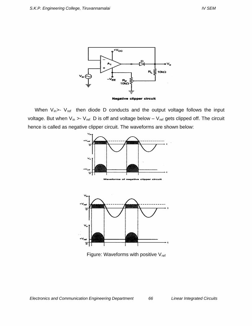
using pot Rp to generate negative voltage Vref. This circuit is shown below:
S.K.P. Engineering College, Tiruvannamalai IV SEM
Electronics and Communication Engineering Department 66 Linear Integrated Circuits
When Vin>- Vref then diode D conducts and the output voltage follows the input
voltage. But when Vin >- Vref D is off and voltage below – Vref gets clipped off. The circuit
hence is called as negative clipper circuit. The waveforms are shown below:
Figure: Waveforms with positive Vref

S.K.P. Engineering College, Tiruvannamalai IV SEM
Electronics and Communication Engineering Department 67 Linear Integrated Circuits
If for the same circuit reference voltage is generated using +Vcc i.e. + Vref the diode D is
on for Vin> Vref and is off for Vin< Vref . The corresponding waveforms are shown in
figure.
12.Explain in detail about clamper circuit with neat waveforms? [CO2-L2-Nov/Dec 2016] Definition: The circuits which are used to add d.c. level as per the requirement to the a.c. output are
called as clamper circuits Sometimes it is necessary to add a d.c. level to the a.c. output
signal. The circuits which are used to add d.c. level as per the requirement to the a.c.
output are called as clamper circuits. These circuits are also called as d.c. restorer
circuits. If the clamped d.c. level is positive the circuits are called as positive clamper
circuits and if clamped level is negative the circuits are called as negative clamper
circuits. Types: (i) Positive clamper circuits
(ii) Negative clamper circuits
Positive clamper circuits: The fig shows the positive clamper circuit using op-amp: When the input voltage
is first time negative due to inverting mode of op-amp the op-amp is positive. This turns
on the diode making it forward biased. Thus the capacitor charges to peak value of
negative cycle of input with the polarities are shown in figure.

S.K.P. Engineering College, Tiruvannamalai IV SEM
Electronics and Communication Engineering Department 68 Linear Integrated Circuits
The diode becomes reverse biased and stops conducting. It becomes open. Hence the
output voltage is sum of the input voltage and the capacitor voltage mathematically it is
given by,
Vout= Vin +Vp
Thus d.c. level equal to Vp gets added in a.c. output signal. The final output waveform
is sinusoidal but shifted positively through Vp.
Hence the circuit is called as positive clamper and the waveform is called as positively
clamped waveform. As during positive half cycle of input, Diode does not conduct the
capacitor retains its voltage at Vp all time after the first negative peak of input.
The waveforms are shown below: It can be observed that waveform swings from 0 to
+2Vp i.e. peak to peak voltage of output waveform is 2 Vp which remains same as the
input voltage. Thus the circuit shows that the total swing of output voltage remains same
as the total swing of input voltage in clamper circuit.
In the circuit given below the d.c. level added is equal to peak value of input used.
Another circuit in which variable positive d.c. level can be added is shown below:

S.K.P. Engineering College, Tiruvannamalai IV SEM
Electronics and Communication Engineering Department 69 Linear Integrated Circuits
The input voltage is applied to the inverting terminal of op-amp A1 while variable
positive d.c. Voltage is applied to the noninverting input terminal of op-amp A1. The
circuit can be analysed using the superposition theorem considering only one input active
at a time.
Let Vref is acting along Vin is Zero. For positive Vref the output voltage v is also
positive. Due to this Diode D is forward biased. Hence the circuit acts as a voltage
follower. Hence the net voltage Vo is same as positive Vref.
Now let input at inverting terminal be purely sinusoidal i.e. Vin= Vmsinwt. For negative
half cycle of input Vo’ will be positive and D will conduct. The capacitor C charges through
Diode D to negative peak voltage Vm. During the positive half cycle of input D does not
conduct and capacitor C retains its previous voltage of Vm.
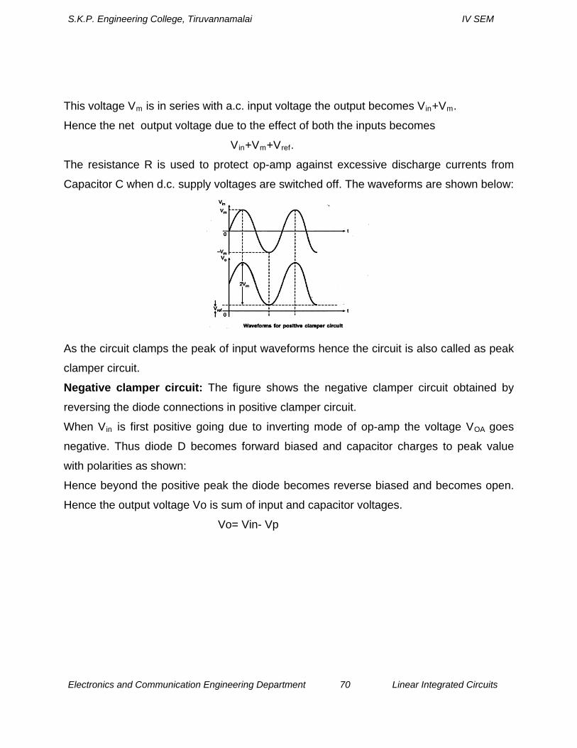
S.K.P. Engineering College, Tiruvannamalai IV SEM
Electronics and Communication Engineering Department 70 Linear Integrated Circuits
This voltage Vm is in series with a.c. input voltage the output becomes Vin+Vm.
Hence the net output voltage due to the effect of both the inputs becomes
Vin+Vm+Vref.
The resistance R is used to protect op-amp against excessive discharge currents from
Capacitor C when d.c. supply voltages are switched off. The waveforms are shown below:
As the circuit clamps the peak of input waveforms hence the circuit is also called as peak
clamper circuit.
Negative clamper circuit: The figure shows the negative clamper circuit obtained by
reversing the diode connections in positive clamper circuit.
When Vin is first positive going due to inverting mode of op-amp the voltage VOA goes
negative. Thus diode D becomes forward biased and capacitor charges to peak value
with polarities as shown:
Hence beyond the positive peak the diode becomes reverse biased and becomes open.
Hence the output voltage Vo is sum of input and capacitor voltages.
Vo= Vin- Vp

S.K.P. Engineering College, Tiruvannamalai IV SEM
Electronics and Communication Engineering Department 71 Linear Integrated Circuits
Hence a negative d.c. level of –Vp gets added to output hence the circuit is called as
negative clamper circuit. The waveforms are shown below:
Another circuit in which variable negative d.c. level can be added is shown below. In such
circuit –Vref is generated using the negative supply –VEE of the op-amp and diode
connections are reversed.
Hence negative clamper is obtained. The waveforms are shown below:

S.K.P. Engineering College, Tiruvannamalai IV SEM
Electronics and Communication Engineering Department 72 Linear Integrated Circuits
Due to opposite connection of diode D, the capacitor charges in reverse direction and
hence negative clamper is obtained. The waveforms are shown above.
13. Differentiate between low pass, high pass, band pass and band reject filter. Sketch the frequency plot. [CO2-L2-Nov/Dec 2016]

S.K.P. Engineering College, Tiruvannamalai IV SEM
Electronics and Communication Engineering Department 73 Linear Integrated Circuits

S.K.P. Engineering College, Tiruvannamalai IV SEM
Electronics and Communication Engineering Department 74 Linear Integrated Circuits
14. Mention two advantages of active filter over passive filter. Also design a second order low pass filter using operational amplifier for the upper cut off frequency of 2 kHz. Assume the value of capacitor to be 0.1 µF. [CO2-H3-Nov/Dec 2015] Advantages of active filters
The active filters have the following advantges over the passive filters :
1. All the elements alongwith op-amp can be used in the integrated form. Hence there
is reduction is size and weight.
2. In large quantities, the cost of the integrated circuit can be much lower than its
equivalent passive network.
3. Due to availability of modem ICs, variety of cheaper op-amps are available.
4. The op-amp gain can be easily controlled in the closed loop fashion hence active
filter input signals is not attenuated.
5. Due to flexibility in gain and frequency adjustments, the active filters can be easily
tuned.
6. The op-amp has high input impedance and low output impedance hence the active
filters using op-amp do not cause loading of the source or load.
7. The inductors are absent in the active filters hence the modem active filters are more
economical.
8. Active filters can be realized under number of class of functions such as Butterworth,
Thomson, Chebyshev,etc.
9. The response is improved as compared to passive filters due to ready availability of
high quality components.
10. The design procedure is simpler than that for the passive filters.
15. Design a first order Low-pass filter for cut-off frequency of 2 KHz and pass-band gain of 2. [CO2-H3]

S.K.P. Engineering College, Tiruvannamalai IV SEM
Electronics and Communication Engineering Department 75 Linear Integrated Circuits
Solution : Given fH = 2kHz and A =2
Let C = 0.01µF
We know that f = 1/ 2πRC
Therefore, R = 1/ 2πfc
= 7.95KΩ
Gain A = 1+(Rf / Ri) = 2
Therefore, Rf = Ri = 10 KΩ. 16. Explain the application nof operational amplifer as differentiator. [CO2-H3-Nov/Dec 2015] Differentiator
An op-amp differentiator or a differentiating amplifier is a circuit configuration which
produces output voltage amplitude that is proportional to the rate of change of the
applied input voltage.
A differentiator with only RC network is called a passive differentiator, whereas a
differentiator with active circuit components like transistors and operational amplifiers is
called an active differentiator. Active differentiators have higher output voltage and
much lower output resistance than simple RC differentiators.

S.K.P. Engineering College, Tiruvannamalai IV SEM
Electronics and Communication Engineering Department 76 Linear Integrated Circuits
Fig. Op-amp differentiator
An op-amp differentiator is an inverting amplifier, which uses a capacitor in series with
the input voltage. Differentiating circuits are usually designed to respond for triangular
and rectangular input waveforms. For a sine wave input, the output of a differentiator is
also a sine wave, which is out of phase by 180o with respect to the input (cosine wave).
Differentiators have frequency limitations while operating on sine wave inputs; the circuit
attenuates all low frequency signal components and allows only high frequency
components at the output. In other words, the circuit behaves like a high-pass filter.

S.K.P. Engineering College, Tiruvannamalai IV SEM
Electronics and Communication Engineering Department 77 Linear Integrated Circuits
Unit -III
Analog Multiplier and PLL
Part A
1. How do you convert a basic multiplier to a squaring and square root circuit? [CO3-L1] For Voltage Squarer: The input voltage Vi to be squared is simply connected to both
the input terminals and hence we have, Vx =Vy = Vi and the output is V0 = KV2i.
For Square rooter: the divider circuit can be used to find the square root of a signal
by connecting both the inputs of the multiplier to the output of the op-amp.
2. What are the applications of PLL for AM detection? [CO3-L1] The PLL can be used as an AM detector for demodulating the amplitude modulated signals.
3. Define : (a) Capture range and (b) Lock range of Phase Locked Loop (PLL) [CO3-L1] Capture range : The range of frequencies over which the PLL can acquire lock with
an input signal is called the capture range. This parameter is expressed as
percentage of fo.

S.K.P. Engineering College, Tiruvannamalai IV SEM
Electronics and Communication Engineering Department 78 Linear Integrated Circuits
Lock-in Range : The range of frequencies over which the PLL can maintain lock with
the incoming signal is called the lock-in range or tracking range. The lock-in range is
expressed as a percentage of fo, the VCO frequency.
4. Mention two applications of analog multiplier. [CO3-L1] Voltage squarer , Frequency doubler
5. What is four quadrant multiplier? [CO3-L1] The four-quadrant operation indicates that the output voltage is directly proportional
to the product of the two input voltages regardless of the polarity of the inputs and
such multipliers can be operated in all the four quadrants of operation.
6. Draw the circuit diagram of a PLL circuit using as a FM detector. [CO3-L1]
7. Enlist any four applications of NE 565 PLL. [CO3-L3] (i) AM detection
(ii) FM detection
(iii) FSK modulation /demodulation

S.K.P. Engineering College, Tiruvannamalai IV SEM
Electronics and Communication Engineering Department 79 Linear Integrated Circuits
(iv) Frequency multiplication
8. Draw the block diagram of IC 566 VCO (Voltage Controlled Oscillator) [CO3-L1]
9.What is meant by frequency synthesizing? [CO3-L1] A frequency synthesizer allows the designer to generate a variety of output frequencies
as multiples of a single reference frequency. The frequency synthesizer produces a
large number of precise frequencies, which are derived from a single reference source
of frequency, a stable crystal controlled oscillator.
10. Define lock range of a PLL. [CO3-L1]

S.K.P. Engineering College, Tiruvannamalai IV SEM
Electronics and Communication Engineering Department 80 Linear Integrated Circuits
The range of frequencies over which the PLL can maintain lock with the incoming signal
is called the lock-in range or tracking range. It is expressed as a percentage of fo , the
VCO frequency.
11. A PLL frequency multiplier has an input frequency of “f” and a decade counter is included in the loop. What will be the frequency of the PLL output? [CO3-L3]
fo = 1 / 10secs
12. Mention any two applications of PLL. [CO3-L1] Frequency translation, AM detection, FM Demodulation, FSK Demodulator.
13. What is a two quadrant multiplier? [CO3-L1] A two quadrant multiplier functions properly if one input is held positive and the other is
allowed to swing in both positive and negative.
14 What are the advantages of variable transconductance technique? [CO3-L2] i. Provides very good accuracy
ii. Provides four quadrant operation
iii. Reduced error atleast by 10 times
15. VCO is also called V-f converter. Why? [CO3-L1] The VCO converts the applied input voltage to an output frequency. Hence, it is called
voltage to frequency converter.
16. What are the advantages of emitter coupled transistor pair? [CO3-L3] i. Low drift because of its symmetrical IC construction.
ii. Very high input resistance
iii. High CMRR

S.K.P. Engineering College, Tiruvannamalai IV SEM
Electronics and Communication Engineering Department 81 Linear Integrated Circuits
17. With a reference to a VCO, define voltage to frequency conversion factor Kv. [CO3-L1] Voltage to frequency conversion factor Kv is defined as
KV = ∆f0 /∆Vc
18. What is VCO? [CO3-L1] The VCO is a free running multivibrator and operates at a set frequency called free
running frequency. This frequency can be shifted to the either side by applying a dc
control voltage. The frequency deviation is directly proportional to the dc control voltage
and hence it is called Voltage Controlled Oscillator.
19. Draw the relation between the capture ranges and lock range in a PLL. [CO3-L1]
20. List the basic building blocks of a PLL? [CO3-L1] A phase locked loop consists to a phase detector, low pass filter, amplifier and a VCO in feedback loop.

S.K.P. Engineering College, Tiruvannamalai IV SEM
Electronics and Communication Engineering Department 82 Linear Integrated Circuits
21. What are the important characteristics of a PLL? [CO3-L1] The important characteristics of a PLL are: lock-in range, capture range and pull-in-time.
22.What is the need of LPF in a PLL? [CO3-L1] The LPF not only removes the high frequency components and noise, but also controls the dynamic characteristics of the PLL. The LPF controls the capture range and lock range of a PLL.
23. Which is greater ‘Capture range’ or ‘Lock-in range’? [CO3-L1] The lock-in range is usually greater than the capture range. The capture range depends upon the LPF characteristics.
24.What is the range of modulation input voltage applied to a VCO? [CO3-L1] The modulating input voltage is usually varied from 0.75 Vcc to Vcc which can produce a frequency variation of about 10 to 1.
25. Mention few monolithic PLL ICs? [CO3-L1] Signetics SE/NE 560 series – 560,561,562,564,565 and 567 are monolithic PLLs.
26. Mention few applications of analog multiplier? [CO3-L1] Frequency doubling, Phase angle detection, Squaring, Multiplication, Division
27. Sketch the schematic symbol of multiplier. [CO3-L1]

S.K.P. Engineering College, Tiruvannamalai IV SEM
Electronics and Communication Engineering Department 83 Linear Integrated Circuits
28. What is transconductance multiplier? [CO3-L1] Log-amps require the input and reference voltages to be of the same polarity. This restricts log-antilog amplifiers to one quadrant operation. A technique that provides four quadrant multiplication is trans-conductance multiplier.
29. What are the types of phase detector? [CO3-L1]
Analog phase detector and Digital Phase detector
30. What are the performance parameters of a multiplier? [CO3-L1] Accuracy, Linearity, Bandwidth, Feed through voltage, Scale factor
31. Define scale factor of multiplier? [CO3-L1] Scale factor is the constant (k) relating the output voltage and the product of two input voltages.
K= Vo / V1V2
32. Define Pull-in time. [CO3-L1] The total time taken by the PLL to establish lock is called pull-in time. It depends on the initial phase and frequency difference between the two signal levels as well as on the overall loop gain and loop filter characteristics.
33. What are the three stages through which PLL operates? [CO3-L3] i. Free running ii. Capture iii. Locked/tracking

S.K.P. Engineering College, Tiruvannamalai IV SEM
Electronics and Communication Engineering Department 84 Linear Integrated Circuits
34. Draw the sketches for (i) One quadrant multiplier (ii) Two quadrant multiplier and (iii) Four quadrant multiplier. [CO3-L3]
35. Draw the basic block diagram of a PLL. [CO3-L1]
Part B 1. State the limitations of emitter coupled transistor pair. [CO3-L1] The first limitation is that V2 is offset by VBE(on). The second is that V2 must always be
positive which results in only a two-quadrant multiplier operation. The third limitation is
that, the tanh (x) is approximated as x. The first two limitations are overcome in the
Gilbert cell.

S.K.P. Engineering College, Tiruvannamalai IV SEM
Electronics and Communication Engineering Department 85 Linear Integrated Circuits
2. Discuss the principle of operation of NE 565 PLL circuit. [CO3-H1-May/June 2016]
Pin Configuration of PLL IC 565: The pin details of PLL IC 565 is shown in the figure.
Basic Block Diagram Representation of IC 565: The signetics NE/SE 560 series is monolithic phase locked loops. The SE/NE 560, 561,
562, 564, 565 & 567 differ mainly in operating frequency range, poser supply
requirements & frequency & bandwidth adjustment ranges.

S.K.P. Engineering College, Tiruvannamalai IV SEM
Electronics and Communication Engineering Department 86 Linear Integrated Circuits
The important electrical characteristics of the 565 PLL are,
• Operating frequency range: 0.001Hz to 500 Khz.
• Operating voltage range: ±6 to ±12v
• Input level required for tracking: 10mv rms min to 3 Vpp max
• Input impedance: 10 K ohms typically.
• Output sink current: 1mA
• Output source current: 10 mA
The center frequency of the PLL is determined by the free running frequency of the VCO,
which is given by fOUT =114
2.1CR
HZ------------(1)
where R1&C1 are an external resistor & a capacitor connected to pins 8 & 9.
• The VCO free-running frequency fOUT is adjusted externally with R1 & C1 to be at the
center of the input frequency range.
• C1 can be any value, R1 must have a value between 2 k ohms and 20 K ohms.

S.K.P. Engineering College, Tiruvannamalai IV SEM
Electronics and Communication Engineering Department 87 Linear Integrated Circuits
• Capacitor C2 connected between 7 & +V.
• The filter capacitor C2 should be large enough to eliminate variations in the
demodulated output voltage in order to stabilize the VCO frequency.
• The lock range fL & capture range fc of PLL is given by,
The lock range fL= ± Vf 8 out Hz ------------------(2)
Where fOUT = free running frequency of VCO (Hz)
V = (+V)-(-V) volts
Capture range fc of PLL is
Fig. PLL block diagram to determine capture range
3.. Explain the application of VCO for FM generation. [CO3-L2] A common type of VCO available in IC form is Signetics NE/SE566. The pin configuration
and basic block diagram of 566 VCO are shown in figures below.

S.K.P. Engineering College, Tiruvannamalai IV SEM
Electronics and Communication Engineering Department 88 Linear Integrated Circuits
Referring to the circuit in the above figure, the capacitor c1 is linearly charged or
discharged by a constant current source/sink. The amount of current can be controlled by
changing the voltage vc applied at the modulating input (pin 5) or by changing the timing
resistor R1 external to the IC chip.
The voltage at pin 6 is held at the same voltage as pin 5. Thus, if the modulating voltage
at pin 5 is increased, the voltage at pin 6 also increases, resulting in less voltage across
R1 and thereby decreasing the charging current.
The voltage across the capacitor C1 is applied to the inverting input terminal of Schmitt
trigger via buffer amplifier. The output voltage swing of the Schmitt trigger is designed to
Vcc and 0.5 Vcc.
If Ra = Rb in the positive feedback loop, the voltage at the non-inverting input terminal of
Schmitt trigger swings from 0.5 Vcc to 0.25 Vcc. When the voltage on the capacitor c1
exceeds 0.5 Vcc during charging, the output of the Schmitt trigger goes LOW (0.5 Vcc).
The capacitor now discharges and when it is at 0.25 Vcc, the output of Schmitt trigger
goes HIGH (Vcc).

S.K.P. Engineering College, Tiruvannamalai IV SEM
Electronics and Communication Engineering Department 89 Linear Integrated Circuits
Since the source and sink currents are equal, capacitor charges and discharges for the
same amount of time. This gives a triangular voltage waveform across c1 which is also
available at pin 4. The square wave output of the Schmitt trigger is inverted by buffer
amplifier at pin 3. The output waveforms are shown near the pins 4 and 3.
Calculation of the output frequency of the VCO:The total voltage on the capacitor
changes from 0.25Vcc to 0.5Vcc .Thus ∆V=0.25 Vcc.The capacitor charges with a constant
current source.
The time period T of the triangular waveform=2 t∆ .The frequency of oscillation fo is
)1(....................25.0
25.0
iCV
t
Ci
tV
Ci
tv
Tcc
T
cc
T
=∆
=∆
=∆∆

S.K.P. Engineering College, Tiruvannamalai IV SEM
Electronics and Communication Engineering Department 90 Linear Integrated Circuits
)2(....................)(2
,
5.0211
ccTT
ccco
T
ccc
Tcco
VCRvV
fTherofore
RvV
i
CVi
tTf
−=
−=
=∆
==

S.K.P. Engineering College, Tiruvannamalai IV SEM
Electronics and Communication Engineering Department 91 Linear Integrated Circuits
Fig. Waveforms for VCO
The output frequency of the VCO can be changed either by (i) RT, (ii) CT or (iii) the
voltage vc at the modulating input terminal pin 5. The voltage vc can be varied by
connecting a R1R2 circuit as shown in the figure below.
The components R1and c1 are first selected so that VCO output frequency lies in the
centre of the operating frequency range. Now the modulating input voltage is usually
varied from 0.75 Vcc to Vcc which can produce a frequency variation of about 10 to 1.

S.K.P. Engineering College, Tiruvannamalai IV SEM
Electronics and Communication Engineering Department 92 Linear Integrated Circuits
4. Draw the block diagram of VCO and explain operation. Also derive the frequency of oscillator. Voltage Controlled Oscillator
Fig. Block diagram of VCO
5. Brief the application of PLL IC for frequency multiplication. [CO3-L3-
Nov/Dec 2016] PLL as Frequency Multiplier.
Fig. PLL as frequency multiplier
For the working of Frequency multiplier circuit the frequency divider is inserted between
the VCO and phase comparator. Since the output of the divider is locked into the input

S.K.P. Engineering College, Tiruvannamalai IV SEM
Electronics and Communication Engineering Department 93 Linear Integrated Circuits
frequency fIN, the VCO is actually running at a multiple of the input frequency. The
desired amount of multiplication can be obtained by selecting a proper divide-by-N
network, where N is an integer. For example, to obtain the output frequency fOUT = 5fIN,
a divide-by-N = 5 network is needed.
6. Explain the application of Phase Locked Loop as CO3-L3-Nov/Dec 2015] (i) Frequency synthesizer (ii) AM demodulator and (iii) FM demodulator (iv) Frequency Shift Keying (FSK) Demodulator The output from a PLL system can be obtained either as the voltage signal vc(t)
corresponding to the error voltage in the feedback loop, or as a frequency signal at VCO
output terminal. The voltage output is used in frequency discriminator applications
whereas the frequency output is used in signal conditioning, frequency synthesis or clock
recovery applications.
Consider the case of voltage output. When PLL is locked to an input frequency, the error
voltage vc(t) is proportional to (fs-fo). If the input frequency is varied as in the case of FM
signal, vc will also vary in order to maintain the lock. Thus the voltage output serves as a
frequency discriminator which converts the input frequency changes to voltage changes.
In the case of frequency output, if the input signal is comprised of many frequency
components corrupted with noise and other disturbances, the PLL can be made to lock,
selectively on one particular frequency component at the input. The output of VCO would
then regenerate that particular frequency (because of LPF which gives output for beat
frequency) and attenuate heavily other frequencies. VCO output thus can be used for
regenerating or reconditioning a desired frequency signal (which is weak and buried in
noise) out of many undesirable frequency signals.
Some of the typical applications of PLL are discussed below.

S.K.P. Engineering College, Tiruvannamalai IV SEM
Electronics and Communication Engineering Department 94 Linear Integrated Circuits
(i)Frequency Multiplier: Fig. 4.63 shows the block diagram for a frequency multiplier using PLL 565.
Here, a divide by N network is inserted between the VCO output (pin 4) and the phase
comparator input (pin 5).
Since the output of the divider is locked to the input frequency fi, the VCO is
actually running at a multiple of the input frequency. Therefore, in the locked state, the
VCO output frequency fo is given by,
fo = Nfi (1)
By selecting proper divider by N network, we can obtain desired multiplication.
For example, to obtain output frequency fo=6 fi, a divide by N should be equal to 6. (ii) Frequency Synthesizer: The PLL can be used as the basis for frequency synthesizer that can produce a
precise series of frequencies that are derived from a stable crystal controlled oscillator.
Fig. 4.65 shows the block diagram of frequency synthesizer. It is similar to frequency multiplier circuit except that divided by M network is
added at the input of phase lock loop. The frequency of the crystal-controlled oscillator is
divided by an integer factor M by divider network to produce a frequency fosc /M, where
fosc is the frequency of the crystal controlled oscillator.

S.K.P. Engineering College, Tiruvannamalai IV SEM
Electronics and Communication Engineering Department 95 Linear Integrated Circuits
The VCO frequency fVCO is similarly divided by factor N by divider network to give
frequency equal to fVCO /N. When the PLL is locked in on the divided-down oscillator
frequency, we will have fosc /M = fVCO /N so that fVCO = (N/M) fosc
PLL as Frequency synthesizer
By adjusting divider counts to desired values large number of frequencies can be
produced, all derived from the crystal controlled oscillator.
(iii)FM Demodulator:
Fig. PLL as FM Demodualtor

S.K.P. Engineering College, Tiruvannamalai IV SEM
Electronics and Communication Engineering Department 96 Linear Integrated Circuits
The PLL can be very easily used as an FM detector or demodulator. Fig. 4.66 shows the
block diagram of FM detector.When the PLL is locked in on the FM signal, the VCO
frequency follows the instantaneous frequency of the FM signal, and the error voltage or
VCO control voltage is proportional to the deviation of the input frequency from the centre
frequency.
Therefore, the a-c component of error voltage or control voltage of VCO will represent a
true replica of the modulating voltage that is applied to the FM carrier at the transmitter.
The faithful reproduction of modulating voltage depends on the linearity between the
instantaneous frequency deviation and the control voltage of VCO. It is also important to
note that the FM frequency deviation and the modulating frequency should remain in the
locking range of PLL to get the faithful replica of the modulating signal.
If the product of the modulation frequency fm and the frequency deviation exceeds the (∆
fc )2, the VCO will not be able to follow the instantaneous frequency variations of the FM
signal.
(iv)Frequency Shift Keying (FSK) Demodulator: In digital data communication, binary data is transmitted by means of a carrier frequency.
It uses two different carrier frequencies for logic 1 and logic 0 states of binary data signal.
This type of data transmission is called frequency shift keying (FSK). In this data transmission, on the receiving end, two carrier frequencies are converted
into I and 0 to get the original binary data. This process is called as FSK
demodulation.A PLL can be used as a FSK demodulator, as shown in the Fig. 4.67. It is similar to the PLL demodulator for analog FM signals except for the addition of a
comparator to produce a reconstructed digital output signal.

S.K.P. Engineering College, Tiruvannamalai IV SEM
Electronics and Communication Engineering Department 97 Linear Integrated Circuits
Let us consider that there are two frequencies, one frequency (f1) is represented as "0"
and other frequency (f2) is represented as "I". If the PLL remain is locked into the FSK
signal at both f1 and f2, the VCO control voltage which is also supplied to the comparator
will be given as
Vc1= (f1- fo ) / Kv and Vc2 = (f 2 - f0) / Kv respectively.
where Kv is the voltage to frequency transfer coefficient of the VCO.
The difference between the two control voltage levels will be ∆Vc = (f2 – f1) / Kv
The reference voltage for the comparator is derived from the additional low pass filter and
it is adjusted midway between Vc1 and Vc2 . Therefore, for Vc1 and Vc2, comparator gives
output '0' and '1', respectively.
(v)AM detection:

S.K.P. Engineering College, Tiruvannamalai IV SEM
Electronics and Communication Engineering Department 98 Linear Integrated Circuits
The PLL is locked to the carrier frequency of the incoming AM signal. Once locked the
output frequency of VCO is same as the carrier frequency, but it is in unmodulated form.
The modulated signal with 90° phase shift and the unmodulated carrier from output of
PLL are fed to the multiplier. Since VCO output is always 90' out of phase with the
incoming AM signal under the locked condition, both the signals applied to the multiplier
are in same phase. Therefore, the output of the multiplier contains both the sum and the
difference signals. The low pass filter connected at the output of the multiplier rejects high
frequency components gives demodulated output. As PLL follows the input frequencies
with high accuracy, a PLL AM detector exhibits a high degree of selectivity and noise
immunity which is not possible with conventional peak detector type AM modulators.
(vi)Frequency Translation: Frequency translation means shifting the frequency of an
oscillator by a small factor.
Fig . Block schematic for frequency translator using PLL

S.K.P. Engineering College, Tiruvannamalai IV SEM
Electronics and Communication Engineering Department 99 Linear Integrated Circuits
It consists of mixer, low pass filter and theP'LL. The input frequency fs which has to be
shifted is applied to the mixer. Another input to the mixer is the output voltage of VCO, fo.
Therefore, the output of mixer contains the sum and difference signal (fo ± fs). The low
pass filter connected at the output of mixer rejects the (fo+fs,) signal and gives only (fo-fs)
signal at the output. The (fo-fs) signal is applied to the phase detector. Another input for
phase detector is the offset frequency f1 .In the locked mode, the VCO output frequency is
adjusted to make two input frequencies of phase detector equal. This gives (fo-fs)= f1 and
fo= fs+ f1.By adjusting offset frequency f1 we can shift the frequency of the oscillator to the
desired value.

S.K.P. Engineering College, Tiruvannamalai IV SEM
Electronics and Communication Engineering Department 100 Linear Integrated Circuits
Unit IV
Analog to Digital And Digital to Analog Converters
Part A
1. What would be produced by a DAC, whose output range is 0 to 10V and whose binary number is 10111100 (for a 8 bit DAC)? [ CO4-L1]
V0 = 10V(1x1/2 + 0x1/22 + 1x1/23 +1x1/24+1x1/25+1x1/26 + 0x1/27 + 0x1/28)
= 10V(1/2 + 1/8 +1/16 +1/32 + 1/64)
= 7.34 V
2. What is over sampling? [ CO4-L1] Oversampling is a process in which additional “oversampling factor-1” zeros are
inserted in to the digital data.
3. Determine the number of comparators and resistors required for 8 bit flash type ADC. [ CO4-L3]
The number of comparators required for 8 bit flash type ADC is 2n-1 ( n is the
number of bits ), hence we need 28-1 comparators.
i.e 256-1 = 255 comparators.
4. Mention two advantages of R-2R ladder type Digital to Analog converter when compared to weighted resistor type Digital to Analog converter. [ CO4-L1] (i) More accurate selection and design of resistors R and 2R are possible
(ii) The binary word length can be increased by adding required number of R-2R
sections.

S.K.P. Engineering College, Tiruvannamalai IV SEM
Electronics and Communication Engineering Department 101 Linear Integrated Circuits
5. A 12 bit D/A converter has resolution of 20 mV/LSB. Find the full scale output voltage.[ CO4-L2]
Resolution =
20 =
Therefore, VOFS = 5.1V
6. Draw the binary ladder network of DAC. If the value of the smaller resistance is 10k. What is the value of the other resistance? [CO4-L1]
7. What are the advantages of inverted R-2R (current type) ladder D/A converter over R-2R (voltage type ) D/A converter. [ CO4-L1] The most important advantage of the current mode or inverted ladder type of D/A
converter is that the stray capacitance do not affect the speed of response of the
circuit due to the constant ladder node voltages.
Speed performance is improved.

S.K.P. Engineering College, Tiruvannamalai IV SEM
Electronics and Communication Engineering Department 102 Linear Integrated Circuits
8. What is the need for electronic switches in D/A converter? [ CO4-L1] The Switches which connects the digital binary input to the nodes of a D/A
converter is an electronic switch. Although switches can be made of using
diodes, Bipolar junction Transistors,Field Effect transistors or MOSFETs, there
are four main configurations used as switches forDACs.
They are
i) Switches using overdriven Emitter Followers.
ii) Switches using MOS Transistor- Totem pole MOSFET Switch and CMOS
Inverter Switch.
iii) CMOS switch for Multiplying type DACs .
iv) CMOS Transmission gate switches.
These configurations are used to ensure the high speed switching operations
for different types ofDACs.
9. Draw a sample and hold circuit. [ CO4-L1]
10. State the principle of single slope A/D converter. [ CO4-L1] The single slope A/D converter compares the unknown analog input voltage with a
reference voltage that begins at 0V and increases linearly with time.

S.K.P. Engineering College, Tiruvannamalai IV SEM
Electronics and Communication Engineering Department 103 Linear Integrated Circuits
11. Mention any two applications of a D/A converter. [ CO4-L1] i. Microprocessor interfacing
ii. CRT graphics representation
iii. Programmable power supplies
iv. Digitally controlled gain circuits.
12. For an n-bit flash type A/D converter, how many comparators are required? State the disadvantage of that type of converter. [CO4-L1] The number of comparators required is 2n -1.
Disadvantage: The number of comparators required almost doubles for each added bit.
The larger the value of n, the more complex is the priority encoder.
13. What output voltage would be produced by a D/A converter whose output range is 0 to 10V and whose input binary number is 0110 for a 4 bit DAC. [CO4-L3] Vo = 10V (0 x ½ + 1x1/22 + 1x1/23+ 0x1/24 )
= 10 ( ¼ + 1/8) = 3.75 V
14. What is the main drawback of dual slope ADC? [CO4-L2] The dual slope ADC has long conversion time. This is the main drawback of dual slope
ADC.
15. Define settling time of D/A converter. [CO4-L1] Settling time represents the time it takes for the output to settle within a specified band
(1/2) LSB of its final value

S.K.P. Engineering College, Tiruvannamalai IV SEM
Electronics and Communication Engineering Department 104 Linear Integrated Circuits
16. What is meant by resolution of a DAC? [CO4-L2] Smallest change in voltage which may be produced at the output (or input) of the
converter.
Resolution (in volts) ( VFS / 2n – 1 ) = 1 LSB increment
17. Which is the fastest ADC? State the reason? [CO4-L2] Parallel comparator (Flash) A/D converter is the fastest ADC because the conversion
takes place simultaneously rather than sequentially.
18. Give the advantages of integrating type ADC. [CO4-L2] (i) The integrating type of ADCs do not need a Sample/Hold circuit at the input.
(ii) It is possible to transmit frequency even in noisy environment or in an isolated form.
19. Define accuracy of a D/A CONVERTER.[CO4-L2] Absolute accuracy: It is the maximum deviation between the actual converter output
and the ideal converter output.
Relative accuracy: It is the maximum deviation after gain and offset errors have been
removed.
20. Compare and contrast Binary ladder and R-2Rladder type DAC. [CO4-H1]
Binary weighted resistor DAC R-2R DAC
(i) (i) Requires a wide range of
resistor values.
(ii) (ii) Due to higher values of
resistor required for the LSB, the use of
weighted resistor DAC in monolithic form
restricted to 8-bits.
(i)Requires only two values to resistor.
(ii) No such restriction as only two resistor
values are used whatever may be the
number of inputs.

S.K.P. Engineering College, Tiruvannamalai IV SEM
Electronics and Communication Engineering Department 105 Linear Integrated Circuits
21.Define resolution time and conversion time of DAC. [CO4-L1] Resolution time: The resolution of a data converter is the smallest change in voltage
which may be produced at the output or input of the converter.
Conversion time: It is defined as the total time required to convert a digital signal to
analog signal.
22. What is a sample and hold circuit? [CO4-L1] It samples an input signal and holds on to its last sampled value until the input is
sampled again.
23. What are the components of a sample and hold circuit? [CO4-L1] (i) n-Channel E-MOSFET (ii) Control Voltage (iii) Capacitor
24. What is sample period and hold period? [CO4-L1] Time period Ts during which the voltage across the capacitor is equal to the input
voltage is called Sample period. Time period TH during which the voltage across the
capacitor is held constant is Hold Period.
25. What are the applications of sample and hold circuit?[CO4-L1]
(i) Digital interfacing
(ii) Analog to digital conversion
(iii) Pulse code modulation systems
26. What are the important specifications of converters? [CO4-L2] Resolution: The resolution of a converter is the smallest change in voltage which may
be produced at the output (or input) of the converter.
Linearity: It gives us how close the converter output is to its ideal transfer
characteristics.
Accuracy : Actual accuracy and Relative accuracy.

S.K.P. Engineering College, Tiruvannamalai IV SEM
Electronics and Communication Engineering Department 106 Linear Integrated Circuits
Actual Accuracy: It is the maximum deviation between the actual converter output and
the ideal converter output.
Relative Accuracy: It is the maximum deviation after gain and offset errors have been
removed.
Monotonicity: For a DAC, it is the onew whose analog output increases for an increase
in digital input.
Settling time: It represents the time it takes for the output to settle within a specified
band.
Part-B
1.With neat block diagram,explain analog to digital converter & digital to analog converter. o Most of the real-world physical quantities such as voltage, current, temperature, pressure
and time etc. are available in analog form. Even though an analog signal represents a real
physical parameter with accuracy, it is difficult to process, store or transmit the analog signal
without introducing considerable error because of the superimposition of noise as in the case
of amplitude modulation.
o Therefore, for processing, transmission and storage purposes, it is often convenient to
express this variable in digital form. It gives better accuracy and reduces noise. The
operation of any digital communication system is based upon analog to digital (A/D) and
digital to analog (D/A) conversion.
o Figure highlights a typical application within which A/D and D/A conversion is used. The
analog signal obtained from the transducer is band limited by antialiasing filter. The signal is
then sampled at a frequency rate more than twice the maximum frequency of the band limited
signal.
o The sampled signal has to be held constant while conversion is taking place in A/D
converter. This requires that ADC should be preceded by a sample and hold (S/H) circuit. The

S.K.P. Engineering College, Tiruvannamalai IV SEM
Electronics and Communication Engineering Department 107 Linear Integrated Circuits
ADC output is a sequence in binary digit. The micro-computer or digital signal processor
performs the numerical calculations of the desired control algorithm.
o The D/A converter is to convert digital signal into analog and hence the function of DAC is
exactly opposite to that of ADC. The D/A converter is usually operated at the same frequency
as the ADC. The output of a D/A converter is commonly a staircase. This staircase-like digital
output is passed through a smoothing filter to reduce the effect of quantization noise.
o The scheme given in Pig. 10.1 is used either in full or in part in applications such as digital
audio recording and playback, computer, music and video synthesis, pulse code modulation
transmission, data acquisition, digital multimeter, direct digital control, digital signal
processing, microprocessor based instrumentation.
Fig. Circuit showing application of A/D and D/A converter
Both ADC and DAC are also known as data converters and are available in 1C form. It may
be mentioned here that for slowly varying signal, sometimes sample and hold circuit may be
avoided without considerable error. The A-D conversion usually makes use of a D-A
converter so we shall first discuss DAC followed by ADC.
2.Define basic DAC techniques. What are the limitations in weighted resistor type D/A converters and explain how this problem can be solved in R-2R ladder D/A converters and inverted R-2R ladder technique and also derive the necessary equations. [CO4-H1- May - 2011) (Dec - 2011) ( May - 2012) ( May – 2014,May 2015) Basic DAC:

S.K.P. Engineering College, Tiruvannamalai IV SEM
Electronics and Communication Engineering Department 108 Linear Integrated Circuits
Where
The schematic of a DAC is shown in Fig. The input is an n-bit binary word D and is combined
with a reference voltage VR to give an analog output signal. The output of a DAC can be
either a voltage or current. For it voltage output DAC, the D/A converter is mathematically
described us
Vo — output voltage
VFS = full scale output voltage
K = scaling factor usually adjusted to unity
d1 d2....dn= n-bit binary fractional word with the decimal point located at the left
d1= most significant bit (MSB) with a weight of VFS/2
dn - least significant bit (LSB) with a weight of VFS/2n
Fig: Schematic of a DAC
Weighted resistor DAC: ( May - 2014)
• One of the simplest circuits shown in Fig.uses a summing amplifier with a binary weighted
resistor network. It has n-electronic switches dI ,d2,...dn controlled by binary input word.
These switches are single pole double throw (SPDT) type.
• If the binary input to a particular switch id 1, the resistance to the reference voltage (-VR).
And if the input bit is 0, the switch, connects the resistor to the ground. From Fig. 10.3(a), the
output current for an ideal op-amp can be written as
• Comparing Eq (10,1) with Eq (I0.2) it can be seen that if Rf = R then K = 1 and VFS = VR.

S.K.P. Engineering College, Tiruvannamalai IV SEM
Electronics and Communication Engineering Department 109 Linear Integrated Circuits
The circuit shown in Fig.(a) uses a negative reference voltage. The analog output voltage is
therefore positive staircase as shown in Fig. (b) for a 3-bit weighted resistor DAC.
It may be noted that (1)Although the op-amp in Fig. (a) is connected in inverting mode, it can also be connected in
non-inverting mode.
(2)The op-amp is simply working as a current to voltage converter.
(3)The polarity of the reference voltage is chosen in accordance with the type of the switch
used. For example, for TTL compatible switched, the reference voltage should be + 5V and
the output will be negative.
(4)The accuracy and stability of a DAC depends upon the accuracy of the resistors and the
tracking of each other with temperature.
Disadvantages: One of the disadvantages of binary weighted type DAC is the wide range of resistor values
required. It may be observed that for better resolution, the input binary word length has to be
increased. Thus, as the number of bit increases, the range of resistance value increases.
Fig. (a) A simple weighted resistor DAC

S.K.P. Engineering College, Tiruvannamalai IV SEM
Electronics and Communication Engineering Department 110 Linear Integrated Circuits
Fig (b) Transfer characteristics of a 3 bit DAC
R-2R Ladder circuit: (voltage mode R-2R)
• Wide range of resistors are required in binary weighted resistor type DAC. This can be
avoided by using R-2R ladder type DAC where only two values of resistor(R & 2R) are
required.
• It is well suited for integrated circuit realization.
• The typical value of R ranges from 2.6 KΩ to 10 KΩ.
• For simplicity, consider a 3-bit DAC as shown in Fig (a), where the switch position d1,d2,d3
corresponds to the binary word 100. The circuit can be simplified to the equivalent form of
Fig. Then, voltage at node C can be easily calculated by the set procedure of network
analysis as

S.K.P. Engineering College, Tiruvannamalai IV SEM
Electronics and Communication Engineering Department 111 Linear Integrated Circuits
Fig(a) R-2R ladder DAC , Fig (b) Equivalent circuit of (a) , Fig (c) Equivalent circuit of (b)
The switch position corresponding to the binary word 001 in 3 bit DAC is shown in Fig, 10.6
(a). The circuit can be simplified to the equivalent form of Fig. 10.6 (b). The voltages at the
nodes (A, B, C) formed by resistor branches are easily calculated in a similar fashion and the
output voltage becomes
Inverted R-2R Ladder: (Current mode R-2R)

S.K.P. Engineering College, Tiruvannamalai IV SEM
Electronics and Communication Engineering Department 112 Linear Integrated Circuits
o In weighted resistor type DAC And R-2R ladder type DAC, current flowing in the resistors
changes as the input data changes. More power dissipation causes heating, which in turn,
creates non-linearity in DAC.
o This is a serious problem and can be avoided completely in Inverted R-2R ladder type DAC.
A 3-bit Inverted R-2R ladder type DAC is shown in Fig. 10.7 (a) where the position of MSB
end LSB is interchanged.
o Here each input binary word connects the corresponding switch either to ground or to the
inverting input terminal of the op- amp which is also at virtual ground, Since both the terminals
of switches are at ground potential, current flowing1 in the reactances is constant and
independent of switch position, i.e. independent of input binary word.
o In Fig, 10.7 (a), when switch di is at logical 0 i.e., to the left, the current through 2R resistor
flows to the ground and when the switch di is at logical ‘1’ ie„ to the right, the current through
2R sinks to the virtual ground. The circuit has the important property that the currents divides
equally at each of the nodes. This is because the equivalent resistance to the right or to the
left of any node is exactly 2 R. The division of the current is shown, in fig.10.7 (b).
o Consider a reference current of 2 mA. Just to the right of node A.Similarly to the right of
node B,the equivalent resistor is 2 R .Thus 1 mA of current further divides to value 0.5 mA at
node B. Similarly, current divides -equally at node C to 0.25 mA. The equal division of current
in successive nodes remains the same in the 'inverted R-2R ladder irrespective of the input
binary word. Thus the Currents remain constant in each branch of the ladder.

S.K.P. Engineering College, Tiruvannamalai IV SEM
Electronics and Communication Engineering Department 113 Linear Integrated Circuits
Fig (a) Inverted R-2R ladder DAC
Fig (b) Inverted R-2R ladder DAC showing division of current for digital input word 001
3.Define sample ane hold circuit.With neat diagram explain sample and hold circuit and also give the advantages and applications. [CO4- H1- (May - 2010) ( Dec - 2010) (Dec - 2011) ] Sample & hold circuit: o A sample and hold circuit samples an input signal and holds on to its Last sampled value
until the input is sampled again. This type of circuit is very useful in digital interfacing and
analog to digital and pulse code modulation systems.

S.K.P. Engineering College, Tiruvannamalai IV SEM
Electronics and Communication Engineering Department 114 Linear Integrated Circuits
o One of the simplest practical sample and hold circuit configuration is shown in Fig. 4.17 (a).
The n-channel E-MOSFET works as a switch and is controlled by the control voltage vc and
the capacitor C stores the charge.
o The analog signal vi to be sampled is applied to the drain of E-MOSFET and the control
voltage vc is applied to its gate.When v is positive, the E MOSFET turns on and the capacitor
C charges to the instantaneous value of input vi with a time constant [R0 + rDS(ON)]C.Here R0
is the output resistance of the MOSFET when ON.
o Thus the input voltage vi appears across the capacitor C and then at the output through the
voltage follower A2 .
o During the time when control voltage vc is zero,the E-MOSFET is off. The capacitor C is
now facing the high input impedance of the voltage follower A2 and hence cannot discharge.
o The capacitor holds the voltage across it. The time period Ts the time during which voltage
across the capacitor is equal to input voltage called sample period.
o The time period TH during which the voltage across the capacitor is held constant is called
hold period. The frequency of the control voltage should be kept higher than the input so as
to retrieve the input waveform. A low leakage capacitor such as polystyreme, Mylar or Teflon
should be used to retain the storage charge.
Fig. Sample and Hold Circuit

S.K.P. Engineering College, Tiruvannamalai IV SEM
Electronics and Communication Engineering Department 115 Linear Integrated Circuits
Fig. Input and Output waveforms
Advantages of Sample and Hold Circuits 1. The primary use of the sample and hold circuit to hold the sampled analog input voltage
constantduring conversion time of A/D converter.
2. In case of multichannel ADCs, synchronization can be achieved by sampling signals from
all channels at the same time.
3. It also reduces the crosstalk in the multiplexer.
Applications of Sample and Hold Circuits The applications of such sample and hold circuit arc :
Digital interfacing.
Analog to digital converter circuits.
Pulse modulation systems.
In storage of outputs of a multiplexer between updates in data distribution systems.
In reset-stabilised op-amps.

S.K.P. Engineering College, Tiruvannamalai IV SEM
Electronics and Communication Engineering Department 116 Linear Integrated Circuits
In analog demultiplexers.
4.Write ADC/DAC specifications.(or)Explain resolution,linearity,monotonocity,stability and settling time. [CO4-H2- Dec – 2012] DAC /ADC specifications: Both D/A and A/D converters are available with wide range of specifications. The various
important specifications of converters generally specified by the manufacturers are analyzed.
(1)Resolution: The resolution of a converter is the smallest change in voltage which may be
produced at the output (or input) of the converter. For example, an 8-bit D/A converter has 28-
l = 255 equal intervals. Hence the smallest change in output voltage is (1/255) of the full scale
output range.In short, the resolution is the value of the LSB
(2)Linearity:The linearity of an A/D or D/A converter is an important measure of its accuracy
and tells us how close the output is to its ideal transfer-characteristics. In an ideal DAC, equal
increment in the digital input should produce equal increment in theanalog output and the
transfer curve should be linear.
(3)Monotonocity: A motiotonic DAG is the one whose analog output increases for an
increase in -digital input. Figure. represents the transfer curve for a non-mono tonic DAC,
since the output decreases when input code changes from 001 to 010. A monotonic
characteristic is essential in control applications, otherwise oscillations can result.

S.K.P. Engineering College, Tiruvannamalai IV SEM
Electronics and Communication Engineering Department 117 Linear Integrated Circuits
(4)Settling time: The most important dynamic parameter is. the settling time. It represents
the time it takes for the output to settle within a specified band ± (1/2) LSB of its final value
following a code change at the input (usually a full scale change). It depends upon the
switching time of the logic circuitry due to internal parasitic capacitances and inductances.
Settling time ranges from 100 ns to 10 us depending on word length and type of circuit used.
(5)Stability; The performance of converter changes with temperature, age and power supply
variations. So all the relevant parameters, such as offset, gain, linearity error and
monotonicity must be specified over the full temperature and power supply ranges.
5.Explain any two analog to digital converter(or)With neat circuit diagram.explain flash type and successive approximation type ADC. [CO4- H2 -(May - 2010) ( Dec - 2010) ( May – 2012,May 2015,16) ( Dec - 2013) (Nov/Dec 2016)] DIRECT TYPE ADCs 1.The parallel comparator/Flash This is the simplest possible A/D Converter.It is at the same time the fastest and most
expensive technique.Fig shows a 3-bit A/D converter.
The circuit consists of a resistive divider network, 8 op-amp comparators and a 8-line to 3-line
priority encoder.The comparator and its truth table is shown in fig.A small amount of
hysteresis is built into the comparator to resolve any problems that might occur if both inputs

S.K.P. Engineering College, Tiruvannamalai IV SEM
Electronics and Communication Engineering Department 118 Linear Integrated Circuits
were of equaI voltage as shown in the truth table. Coming back to Fig. 10.10 (a), at each
node of the resistive divider, a comparison voltage is available.
Since all the resistors are or equal value, the voltage levels available at the nodes are equally
divided between the reference voltage VR and the ground. The purpose of the circuit is to
compare the analog input voltage Vin with each of the node voltages. The truth table for the
flash type A/D converter is shown in fig. 10,10 (c).
Advantage: The circuit has the advantage of high speed as the conversion take place simultaneously
rather than sequentially. Typical conversion time is l00 ns or less.
Conversion time is limited only by the speed of the comparator and of the priority encoder. By
using an Advanced Micro Devices AMD 686A comparator and a T1147 priority encoder,
conversion delays of the order &f 20 ne can be obtained.

S.K.P. Engineering College, Tiruvannamalai IV SEM
Electronics and Communication Engineering Department 119 Linear Integrated Circuits
Fig. Flash type comparator
Fig. Comparator and its truth table
Fig. Truth table for flash type ADC
Disadvantage The number of comparators- approximately doubles for each added bit. Also the larger the
value of n, the more complex is the priority encoder.
2. Successive approximation technique. In this technique the basic idea is to adjust the DACs input code such that its output is within
+- ½ LSB of the analog input v1 to be A/D converted. the code that achieves this represents
the desired ADC output.
The successive approximation method uses very efficient code searching strategy called
binary search. It completes searching process for n-bit conversion in just n clock periods. It
consists of a DAC,a comparator and a successive approximation register(SAR).

S.K.P. Engineering College, Tiruvannamalai IV SEM
Electronics and Communication Engineering Department 120 Linear Integrated Circuits
The searching code process in successive approximation method is similar to weighing an
unknown material with a balance scale and a set of standard weights. Let us assume that we
have 1 kg,2 kgnd 4 kg weights (SAR) plus a balance scale (comparator and DAC).Now we
will see the successive approximation analogy for 3-bit ADC.
The analog voltage Vin is applied at one input of comparator. On receiving start of
conversion signal (SOC) successive approximation register sets 3-bit binary code 1002 (b2=1)
as an input of DAC. This is similar process of placing the unknown weight on one platform of
the balance and 4 kg weight on the other. The DAC converts the digital word 100 and applies
it equivalent analog output at the second input of the comparator. The Comparator then

S.K.P. Engineering College, Tiruvannamalai IV SEM
Electronics and Communication Engineering Department 121 Linear Integrated Circuits
compares two voltages just like comparing unknown weight with 4 kg weight with the help of
balance scale. If the input voltage is greater than the analog output of DAC, successive
approximation register keeps b2 =1 and makes b1=1(addition of 2kg weight to have total 6 kg
weight ) otherwise it resets b2=0 and makes b1=1 (replacing 2 kg weight). The same process
is repeated for b1 and b0.the status of b0,b1 and b2 bits gives the digital equivalent of the
analog input.
The time for one analog to digital conversion must depend on both the clock’s period T and
number of bits n.It is given as,
TC =T(n+1)
Where TC = conversion time
T = clock period
N = number of bits
The dark lines in the figure shows setting and resetting actions of bits for input voltage 5.2v,
on the basis of comparison. It can be seen from the Figure that one clock pulse is required for
the successive approximation register to compare each bit. However an additional clock pulse
is usually required to reset the register prior to performing a conversion.
6.Explain any two indirect type ADC(or) With neat circuit diagram and wave form of output, explain the working of Dual slope A/D converter. [CO4-H1- (May - 2013) ( Dec - 2013) ( May – 2014,May 2015)] 1.Dual Slope ADC
Dual slope conversion is an indirect method for A/D conversion where an analog
voltage and a reference voltage are converted into time periods by an integrator, and then
measured by a counter. The speed of this conversion is slow but the accuracy is high. Fig.
3.142 shows a typical dual slope converter circuit.
It consists of integrator (ramp generator), comparator, binary counter, output latch and
reference voltage. The ramp generator input is switched between the analog input voltage Vi

S.K.P. Engineering College, Tiruvannamalai IV SEM
Electronics and Communication Engineering Department 122 Linear Integrated Circuits
and a negative reference voltage, —VREF .The analog switch is controlled by the MSB of the
counter. When the MSB is a logic 0, the voltage being measured is connected to the ramp
generator input. When MSB is logic 1, the negative reference voltage is connected to the
ramp generator.
Fig. Integrator output voltage
At time t = 0, analog switch S is connected to the analog input voltage Vi, so that the analog
input voltage integration begins. The output voltage of the integrator can be given as,

S.K.P. Engineering College, Tiruvannamalai IV SEM
Electronics and Communication Engineering Department 123 Linear Integrated Circuits
where RI CI is the integrator time
The integrator output ramp down to a voltage constant and Vi is assumed constant
over the integration time period. At the end of 2N clock periods MSB of the counter goes high.
As a result the output of the flip-flop goes high, which causes analog switch S to be switched
from Vito —VR. At this very same time the binary counter which has gone through its entire
count sequence is reset.
The negative input voltage (—VR) connected to the input of integrator causes the
integrator output to ramp positive. When integrator output reaches zero, the comparator
output voltage goes low, which disables the clock AND gate. This stops the clock pulses
reaching the counter, so that the counter will be stopped at a count corresponding to the
number of clock pulses in time t2.
V and get back upto 0. Therefore, the charge voltage is equal to discharge voltage and
we can write,
The above equation shows that t2 is directly proportional only to the Vi. since VR and t1 are
constants. The binary digital output of the counter gives corresponding digital value for time
period t 2 and hence it is also directly proportional to input signal Vi. The actual conversion of
analog voltage Vininto a digital count occurs during t2. The control circuit connects the clock to
the counter at the beginning of t2. The clock is disconnected at the end of t2. Thus the counter

S.K.P. Engineering College, Tiruvannamalai IV SEM
Electronics and Communication Engineering Department 124 Linear Integrated Circuits
contents is digital output. Hence we can write,
The counter output can then be connected to an appropriate digital display.
Advantages 1. It is highly accurate.
2. Its cost is low.
3. It is immune to temperature caused variations in R1 and C1.
Disadvantage The only disadvantage of this ADC is its speed which is low.
2.Voltage to Time Converter ADC: (May - 2013) (or)With functional block diagram explain A/D converter using voltage to time converter with input and output waveforms.(Nov/Dec 2016) The voltage to time conversion can be easily obtained by using voltage to frequency
converter. Infact as the time is reciprocal of the frequency, the frequency output of voltage
to frequency converter can be easily converted to time using a counter, monostable
multivibrator and a latch. The block diagram of voltage to time converter is shown in the
Fig.
A negative going pulse is used to trigger the monostable multivibrator. The same pulse is
used to reset the counter. The input voltage is applied to the voltage to frequency
converter. It produces the output pulses whose frequency is linearly proportional to the
input.
When the trigger is applied to the monostable multivibrator its output goes high for the
particular time period. At the same time the counter starts counting the pulses. After the
time period of monostable multivibrator, its output goes low.

S.K.P. Engineering College, Tiruvannamalai IV SEM
Electronics and Communication Engineering Department 125 Linear Integrated Circuits
This output is applied to the latch which is negative edge triggered. Hence the counter
output gets latched. The number of pulses which occur during the specific time period are
counted and the latched output is then displayed by the decade counting. .
Fig. Voltage to Time converter
7.Explain Over sampling A/D converter. [CO4-L3-May - 2011) In conventional A/D converters (the so-called Nyquist rate category) the input signal is
sampled at a rate that is only twice that of the band of the input signal itself. The digital
output, generated at the same rate, following to the sampling theorem, retains alt the
informative contents of the input signal which represents it. However, in order to avoid
aliasing, the input signal must be band-limited by an anti-aliasing filter before sampling.Such
analog filters suffer from limitations such as noise, distortion, group delay, and passband
ripple; unless great care is taken, it is difficult for downstream A/D converters to achieve
resolution beyond 18-bits. In many applications, brick-wall analog anti-aliasing filters and SAR
A/D converters have been replaced by over sampling A/D converters with digital filters.
A/D converter where the input signal is sampled much faster than the Nyquist rate, is called
an over sampling A/D converter The signal bandwidth of the input signal is denoted by fb and
the Nyquist rate, which is the minimum sampling frequency required to avoid aliasing, equals

S.K.P. Engineering College, Tiruvannamalai IV SEM
Electronics and Communication Engineering Department 126 Linear Integrated Circuits
The over sampling ratio is defined as the ratio between the sampling frequency and the
Nyquist rate. In other words, it indicates how much faster the input signal is sampled than
minimally required by the Nyquist theorem,
The principle of using over sampling is that by sampling ihe signal many times, errors due to
noise and coarse quantization arc averaged out. Through the use of loop-filter and feedback,
the noise is shaped to high frequencies, which can be easily removed by digital filters.
Fig. Block diagram of oversampled ADC
Anti-aliasing filter (AAF): It eliminates spectral components above half the sampling
frequency from the input signal so that the modulator input signal is band-limited and the
subsequent sampling operation does not alias input signals from higher frequencies into the
band of interest.
LA Modulator : It performs the actual A/D conversion by means of sampling and quantizing
the band-limited input signal as well as by filtering the quantization error from the internal
quantizer out of the in-band. The internal feedback DAC is commonly implemented with the
S.K.P. Engineering College, Tiruvannamalai IV SEM
Electronics and Communication Engineering Department 127 Linear Integrated Circuits
same low resolution as the internal quantizer and thus does not introduce an additional
quantization error.
Decimation filter : After quantization, a digital low pass filter uses decimation both to reduce
the sampling frequency to a nominal rate and prevent aliasing at the new, lower sampling
frequency. Quantized data words are output at a lower frequency (for example, 48 or 96 kHz).
The decimation low pass filter removes frequency components beyond the Nyquist frequency
of the output sampling frequency to prevent aliasing when the output of the digital filter is
resampled (under-sampled) at the system's sampling frequency.
The decimator typically consists of two different blocks. First, a digital low pass filter is used to
remove all the frequency components above — to avoid signal degradation due to aliasing in
the down sampling block that follows the digital filter. This digital filter also removes all the
quantization noise which does not fall inside the signal band. The digital filter operates in the
digital domain and its output contains N-bits words.
The next block in the decimation filter down-samples the output of the digital filter. Down-
sampling by a ratio of OSR can be done by simply keeping a sample and remove the next
OSR-1 samples. Since the sampling rate of signal is changed, aliasing can occur. However,
the decimation process does not result in loss of information since the digital filter removes all
the components that could alias in the signal band.
8.With necessary circuit diagram ,explain single slope ADC . [CO4-L3- May – 2014] Single slope ADC: It consists of a ramp generator and BCD or binary counters. The Fig. 3.140 shows the single
slope ADC

S.K.P. Engineering College, Tiruvannamalai IV SEM
Electronics and Communication Engineering Department 128 Linear Integrated Circuits
At the start, the reset signal is provided to the ramp generator and the counters. Thus
counters are resetted to 0's. The analog input voltageVin is applied to the positive terminal of
the comparator. As this is more positive than the negative input, the comparator output goes
high. The output of ramp generator is applied to the negative terminal of the comparator. The
high output of the comparator enables the AND gate which allows clock to reach to the
counters and also this high output starts the ramp.
The ramp voltage goes positive until it exceeds the input voltage. When it exceeds
Vin,comparator output goes low. This disables AND gate which in turn stops the clock to the
counters. The control circuitry provides the latch signal which is used to latch the counter
data. The reset signal resets the counters to 0's and also resets the ramp generator. The
latched data is then displayed using decoder and a display device.
The main limitations of this circuit are,
Its resolution is less. Hence for applications which require resolution of 9 part in 20,000 or
more, this ADC is not stable.
Variations in ramp generator due to time, temperature or input voltage sensitivity also cause a
lot of problems

S.K.P. Engineering College, Tiruvannamalai IV SEM
Electronics and Communication Engineering Department 129 Linear Integrated Circuits
9.Explain switches for D/A converters.[CO4-L3-May 2016] JFET can be used as an analog switch. For this, the gate-source voltage VGS is restricted to
two values : 0 V or a large negative voltage. The negative voltage must be equal to or more
than VGS(OFF)When VGS is zero, the JFET operates in the ohmic region and JFET acts as a
closed switch. When VGS is more negative than VGS(OFF), the JFET is cut off and the switch is
open.
1.Shunt Switch Fig. 8.5 shows JFET used as a shunt switch. The JFET is turned on and off by VGS. When
VGS =0 V, JFET acts as a closed switch and RDS is much less than RD. Due to the voltage
divider action Vout is very small, approximately equal to 0 V. When VGS is more negative than
VGS(OFF), the JFET acts as an open switch. Due to this Voutis equal to Vin

S.K.P. Engineering College, Tiruvannamalai IV SEM
Electronics and Communication Engineering Department 130 Linear Integrated Circuits
Series Switch Fig. 8.6 shows JFET used as a series switch. When Vgs = 0 V, the switch is
closed and Voutequals Vin. When VGS is equal to or more negative than VGS(OFF) ,the JFET is
open and Vout is approximately zero.
10.State the significance of using high speed sample and hold circuits.Explain its working principle.[CO4-L3-May 2016]

S.K.P. Engineering College, Tiruvannamalai IV SEM
Electronics and Communication Engineering Department 131 Linear Integrated Circuits
A sample and hold circuit samples an input signal and holds on to its last sampled value until
the input is sampled again. This type of circuit is very useful in digital interfacing and analog
to digital and pulse code modulation systems. One of the simplest practical sample and hold
circuit configuration is shown in Fig. The n-channel E-MOSFET works as a switch and is
controlled by the control voltage to., and the capacitor C stores the charge. The analog signal
s, to be sampled is applied to the drain of E-MOSFET and the control voltage u, is applied to
its gate. When u, is positive, the E-MOSFET turns on and the capacitor C charges to the
instantaneous value of input ei with a time constant [(R. + rns (on)] C. Here R„ is the output
resistance of the voltage follower A, and ros (on) is the resistance of the MOSFET .

S.K.P. Engineering College, Tiruvannamalai IV SEM
Electronics and Communication Engineering Department 132 Linear Integrated Circuits
During the time when control voltage u, is zero, the EMOSFET is off. The capacitor C is now
facing the high input impedance of the voltage follower A2 and hence cannot discharge. The
capacitor holds the voltage across it. The time period Ts, the time during which voltage
across the capacitor is equal to input voltage is called sample period. The time period TH of
u, during which the voltage across the capacitor is held constant is called hold period. The
frequency of the control voltage should be kept higher than (at least twice) the input so as to
retrieve the input from output waveform. A low leakage capacitor such as Polystyrene, Mylar,
or Teflon should be used to retain the stored charge.

S.K.P. Engineering College, Tiruvannamalai IV SEM
Electronics and Communication Engineering Department 133 Linear Integrated Circuits
Unit -V
Waveform Generators and Special Function ICs
Part A
1. State the two conditions for oscillations. [CO5-L1-April /May 2015] The two basic conditions for oscillations are :
(i) The magnitude of the loop gain Avβ must be unity
(ii) The total phase-shift of the loop gain Avβ must be equal to 00 or 3600
2. Draw the functional block diagram of 723 regulator. [CO5-L1- April/May 2015]
3. What is the purpose of connecting a capacitor at the input and output side
of an IC voltage regulator? [CO5-L3- Nov/Dec 2015] Two capactiors C1 and C2 are connected on the input and output sides. The output capacitor C2 helps in isolating the effect of transients that may appear on
S.K.P. Engineering College, Tiruvannamalai IV SEM
Electronics and Communication Engineering Department 134 Linear Integrated Circuits
the regulated supply line. C2 is a high quality tantalum capacitor with capacitance of around 1.0µF connected close to the regulator using short connecting leads in order to improve the stability of the output.
4. A Hartley oscillator has L1 = 10 mH, L2 = 5 mH and C = 200 pF.Calculate the frequency of oscillation. [CO5-L3 –May/June 2016] Here M=0 then,LT=L1+L2=15mH
=92.59HZ.
5. What is an isolation amplifier? Mention its applications. [CO5-L1-May/June 2016] An isolation amplifier is an amplifier in which, there is no physical contact
between the input and output sections. These amplifiers are used in applications
requiring very large common-mode voltage difference between the input and
output sections. They find use in medical instrumentation applications, where the
patient must be isolated and protected from leakage currents.

S.K.P. Engineering College, Tiruvannamalai IV SEM
Electronics and Communication Engineering Department 135 Linear Integrated Circuits
6. Draw the block schematic of IC 555 timer. [CO5-L1-Nov/Dec 2016]
7. What is the function of a voltage regulator? Name few IC voltage
regulators. [CO5-L2-Nov/Dec 2016] The voltage regulators are classified into two types.
Linear voltage regulators
Switching regulators
1.Series voltage regulator
1.Transformer based type
2.Shunt voltage regulator
2.Buck switched type
3. Boost switched type

S.K.P. Engineering College, Tiruvannamalai IV SEM
Electronics and Communication Engineering Department 136 Linear Integrated Circuits
8. State the applications of 555 Timer IC. [CO5-L3] Missing pulse detector (Monostable mode)
Linear ramp generator (Monostable mode)
Frequency divider (Monostable mode)
FSK generator (Astable mode)
Pulse position modulator (Astable mode)
9. Define line regulation with respect to a voltage regulator. [CO5-L1]
It is defined as the percentage change in the output voltage for a change in the
input voltage. It is usually expressed in millivolts or as a percentage of the output
voltage.
10. Give the formula for period of oscillations in an op-amp astable circuit. [CO5-L2] The period of the output waveform is determined by the RC time constant of the
two timing components and the feedback ratio established by the R1, R2 voltage
divider network which sets the reference voltage level. If the positive and
negative values of the amplifiers saturation voltage have the same magnitude,
then t1 = t2 and the expression to give the period of oscillation becomes:
T = 2RCln
Then we can see from the above equation that the frequency of oscillation for an
Op-amp Multivibrator circuit not only depends upon the RC time constant but
also upon the feedback fraction.

S.K.P. Engineering College, Tiruvannamalai IV SEM
Electronics and Communication Engineering Department 137 Linear Integrated Circuits
11. Define duty cycle of a periodic pulse wave form. [CO5-L2] The pulse wave has only two possible states: on or off. The most often used
pulse wave is the square wave, which spends exactly the same amount of time in
the "on" position as it does in the "off" position.
The amount of time a pulse wave spends in the "on" position is called its duty cycle. A pulse wave which spends a quarter of the time on, then three quarters
off before repeating, is said to have a 25% duty cycle.
12. What are the limitations of IC 723 general purpose regulator? [CO5-L1] No built in thermal protection
It has no short circuit current limits.
13. What is power amplifier? [CO5-L1] A power amplifier is an electronic device that receives an electrical signal and
reprocesses it to amplify, or increase, its power. The boost in power is achieved
by significantly increasing the input signal’s voltage. A power amplifier is used to
power an output source, such as a stereo speaker, a relay or a motor. One of the
most common functions for a power amplifier is in audio applications.
14. What are the limitations of three terminal regulators? [CO5-L1] No short circuit protection
Output voltage (positive or negative)is fixed.
15. What is a switched capacitor filter? [CO5-L1] A switched capacitor filter is a three terminal element, which consists of
capactiors, periodic switches and operational amplifiers and whose open circuit
voltage transfer function represents filtering characteristics. The operation of the

S.K.P. Engineering College, Tiruvannamalai IV SEM
Electronics and Communication Engineering Department 138 Linear Integrated Circuits
filter is based on the ability of on-chip capacitors and MOS switches to stimulate
resistors. It does not require external reactive components, capacitors or
inductors.
16. Define the duty in astable multivibrator using IC555. [CO5-L1] Duty cycle d = (Tc / T ) x 100
Where T is the total time period and Tc is the charging period.
17. What are the advantages of switched capacitor filter over active filters? [CO5-L1] Low system cost
Low external component count
High accuracy
Good temperature stability
18. What is Opto-coupler? Mention its applications. [CO5-L1] The opto-coupler circuit is a combined package of a photo-emitting device and
a photo-sensing device. The basic opto coupler consists of a LED and a photo
diode.
Application : This can be used as a coupler between any two stages for better
electrical isolation.Capable of wide band signal transmission.

S.K.P. Engineering College, Tiruvannamalai IV SEM
Electronics and Communication Engineering Department 139 Linear Integrated Circuits
19. Draw the internal circuit for audio power amplifier. [CO5-L1]
20. What are the three different wave form generated by ICL8038?[CO5-L1]
Sine wave, Square wave and Triangular waveform
21. Sketch the monostable multivibrator circuit diagram using IC555. [CO5-L2]

S.K.P. Engineering College, Tiruvannamalai IV SEM
Electronics and Communication Engineering Department 140 Linear Integrated Circuits
22. What is meant by thermal shutdown applied to voltage regulator? [CO5-L1] Thermal shutdown means that the chip will automatically turn itself off if the
internal temperature exceeds typically 175 0 C
23. What are the modes of operation of a timer? [CO5-L1] Astable mode and Bistable mode are the two operating modes of a timer.
24. What are the advantages of 723 Voltage regulator? [CO5-L1] The 723 is a general purpose voltage regulator that overcomes the limitations
of three terminal fixed voltage regulators . It is a low current device that can be
employed for load current upto 10A or more by using external components. It can
give adjustable output voltage in a wide range. It provides short circuit protection
and current foldback using external components.
25. What are the applications of LM 380? [CO5-L1] LM 380 is an audio power amplifier which is used for applications such as audio
power amplifier, high gain audio amplifier, intercom system and bridge amplifier.
26. Mention the advantage of foldback current limiting. [CO5-L1] Protecting the load form the over-current protection and protecting the regulator
itself.
27. Mention the advantages of switched capacitor circuits. [CO5-1] i. The compatibility with CMOS process technology
ii. Good accuracy of time constants and (iii) High linearity with voltage

S.K.P. Engineering College, Tiruvannamalai IV SEM
Electronics and Communication Engineering Department 141 Linear Integrated Circuits
28. List all the special application IC’s and its Functions IC Function
SE555 / NE555
Timer
NE/SE 566 Voltage Controlled Oscillator SE/NE560 Phase Locked Loop
LM560 Phase Locked Loop
SE/NE 5018 8-bit DAC
MC1408 8-bit DAC
ICL 8038 Function generator
LM137/LM337 Adjustable Negative Voltage
regulators
IC 723 General Purpose Voltage
Regulator
78xx/ 79xx General Purpose Voltage
Regulator
MC3420 /3250 Monolithic Switching Regulator
µA 78S40 Monolithic Switching Regulator
LM 380 Audio Power amplifier
LM 733 Video amplifier
IC ISO 100 Isolation amplifier
AD293 ,AD294 Isolation amplifier

S.K.P. Engineering College, Tiruvannamalai IV SEM
Electronics and Communication Engineering Department 142 Linear Integrated Circuits
Part B 1. Explain the functional block diagram of IC 555 Timer.[CO5 – H1-May/June 2016) The 555 is a monolithic timing circuit that can produce accurate & highly stable time delays or
oscillation.
The timer basically operates in one of two modes: either
1. Monostable (one - shot) multivibrator or
2. Astable (free running) multivibrator
The important features of the 555 timer are these: 1. It operates on +5v to +18 v supply voltages
2. It has an adjustable duty cycle
3. Timing is from microseconds to hours
4. It has a current o/p PIN CONFIGURATION OF 555 TIMER:
Pin description: Pin 1: Ground: All voltages are measured with respect to this terminal.

S.K.P. Engineering College, Tiruvannamalai IV SEM
Electronics and Communication Engineering Department 143 Linear Integrated Circuits
Pin 2: Trigger: The o/p of the timer depends on the amplitude of the external trigger pulse applied to this pin.
Pin 3: Output: There are 2 ways a load can be connected to the o/p terminal either between pin3 & ground
or between pin 3 & supply voltage
(Between Pin 3 & Ground ON load )
(Between Pin 3 & + Vcc OFF load )
When the input is low:
The load current flows through the load connected between Pin 3 & +Vcc in to the output
terminal & is called the sink current.
When the output is high:
The current through the load connected between Pin 3 & +Vcc (i.e. ON load) is zero. However
the output terminal supplies current to the normally OFF load. This current is called the source
current.
Pin 4: Reset: The 555 timer can be reset (disabled) by applying a negative pulse to this pin. When the
reset function is not in use, the reset terminal should be connected to +Vcc to avoid any false
triggering. Pin 5: Control voltage: An external voltage applied to this terminal changes the threshold as well as trigger voltage.
In other words by connecting a potentiometer between this pin & GND, the pulse width of the
output waveform can be varied. When not used, the control pin should be bypassed to ground
with 0.01uF capacitor to prevent any noise problems.
Pin 6: Threshold: This is the non inverting input terminal of upper comparator which monitors the voltage
across the external capacitor.
Pin 7: Discharge:

S.K.P. Engineering College, Tiruvannamalai IV SEM
Electronics and Communication Engineering Department 144 Linear Integrated Circuits
This pin is connected internally to the collector of transistor Q1.
When the output is high Q1 is OFF.
When the output is low Q is (saturated) ON.
Pin 8: +Vcc: The supply voltage of +5V to +18V is applied to this pin with respect to ground.
Block Diagram of 555 Timer IC: From the above figure, three 5k internal resistors act as voltage divider providing bias voltage
of 2/3 Vcc to the upper comparator & 1/3 Vcc to the lower comparator. It is possible to vary time
electronically by applying a modulation voltage to the control voltage input terminal (5).
i) In the Stable state: The output of the control FF is high. This means that the output is low because of power
amplifier which is basically an inverter. Q = 1; Output = 0
(ii)At the Negative going trigger pulse: The trigger passes through (Vcc/3) the output of the lower comparator goes high & sets the
FF. Q = 1; Q = 0
(iii) At the Positive going trigger pulse: It passes through 2/3Vcc, the output of the upper
comparator goes high and resets the FF. Q = 0; Q = 1
The reset input (pin 4) provides a mechanism to reset the FF in a manner which overrides the
effect of any instruction coming to FF from lower comparator

S.K.P. Engineering College, Tiruvannamalai IV SEM
Electronics and Communication Engineering Department 145 Linear Integrated Circuits
.
2.Draw the functional diagram and applications of Monostable multivibrator using IC 555 timer (May-2010),(Nov-2010),(May-2011),(Dec-2011),(Dec-2010) M ono s t a b l e M u l t i v i b r a t o r u s i n g I C 5 55 : The IC 555 timer can be operated as a monostable multivibrator by connecting an
external resistor and a capacitor as shown in the Fig.
The circuit has only one stable state. When trigger is applied, it produces a pulse at
the output and returns back to its stable state.
• The duration of the pulse depends on the values of R and C. As it has only one stable
state, it is called one shot multivibrator.

S.K.P. Engineering College, Tiruvannamalai IV SEM
Electronics and Communication Engineering Department 146 Linear Integrated Circuits
Operation:The flip-flop is initially set i.e. Q is high. This drives the transistor Qd in saturation.
The capacitor discharges completely and voltage across it is nearly zero. The output at pin 3 is
low.
• When a trigger input, a low going pulse is applied, then circuit state remains unchanged till
trigger voltage is greater than 1/3 Vcc. When it becomes less than 1/3 Vcc, then comparator 2
output goes high.
• This resets the flip-flop so Q goes low and goes high. Low Q makes the transistor Qd off.
Hence capacitor starts charging through resistance R. as shown by dark arrows in the Fig.
• The voltage across capacitor increases exponentially. This voltage is nothing but the
threshold voltage at pin 6. When this voltage becomes more than 2/3 Vcc , then comparator 1
output goes high.
• This sets the flip-flop i.e. Q becomes high and low. This high Q drives the transistor Qd in
saturation. Thus capacitor C quickly discharges through Qd as shown by dotted arrows in the
Fig.So it can be noted that V out at pin 3 is low at start, when trigger is less than 1/3 Vcc it
becomes high and when threshold is greater than 2/3 Vcc. again becomes low, till next trigger
pulse occurs. So a rectangular wave is produced at the output.

S.K.P. Engineering College, Tiruvannamalai IV SEM
Electronics and Communication Engineering Department 147 Linear Integrated Circuits
Summary of monostable operation:
• The pulse width of this rectangular pulse is controlled by the charging time of capacitor.
This depends on the time constant RC. Thus RC controls the pulse width. The waveforms
are shown in the Fig.

S.K.P. Engineering College, Tiruvannamalai IV SEM
Electronics and Communication Engineering Department 148 Linear Integrated Circuits
Calculation of Time period (or) Pulse Width:
• The voltage across the capacitor is given by
vc=Vcc(1-e-t/RC)
At t=T,vc=(2/3)Vcc
Therefore, (2/3)Vcc= Vcc(1-e-T/RC)
(2/3)Vcc= Vcc- Vcc e-T/RC
(2/3)Vcc- Vcc=- Vcc e-T/RC
-1/3= e-T/RC
Taking ln on both sides,
ln(-1/3)=ln e-T/RC
-T/RC=ln(3)
-T/RC=-1.09
T=1.1RC (seconds)

S.K.P. Engineering College, Tiruvannamalai IV SEM
Electronics and Communication Engineering Department 149 Linear Integrated Circuits
Applications of Monostable Multivibrator Frequency Divider:
We know that, in monostable multivibrator, application of trigger pulse gives a positive going pulse on the output. The same monostable circuit can be used as a frequency divider if the timing interval is adjusted to be longer than the period of the input signal, as shown in the Fig.
The Fig.shows monostable multivibrator as a divider-by-2 circuit. Here, timing interval 't' is kept slightly larger than the time period T of the trigger input signal.
The monostable multivibrator will be triggered by the first negative going edge of the trigger input, which will make output to go in its high state. The output will remain high.For the period equal to 'timing interval'.
As timing interval is greater than time period of the trigger input, output will still be high when the second negative going pulse occurs. The monostable will, however, be re-triggered on the third negative-going pulse.
Therefore, monostable triggers on every other pulse of the trigger input, so there is only one output for every two input pulses, thus trigger signal is, divided by 2.In this way, by adjusting the timing interval, the monostable circuit can be made integral fractions of the frequency of the input trigger signal.

S.K.P. Engineering College, Tiruvannamalai IV SEM
Electronics and Communication Engineering Department 150 Linear Integrated Circuits
Pulse Width Modulation:
• Fig. shows pulse width modulator. It is basically a monostable multivibrator with a modulating
input signal applied at the control voltage input (pin 5).Internally, the control voltage is adjusted
to the 2/3 Vcc.
• Externally applied modulating signal changes the control voltage, and hence the threshold
voltage level of the upper comparator (comparator 1). As a result, time period required to
charge the capacitor up to threshold voltage levels changes giving pulse width modulated
signals at the output.
• It may be noted from the output waveform that the pulse duration varies according to the
modulating signal level, but the frequency of the output pulses is same as that of the trigger
input signal.

S.K.P. Engineering College, Tiruvannamalai IV SEM
Electronics and Communication Engineering Department 151 Linear Integrated Circuits
Other Applications of monostable multivibrator: The various other applications of IC 555 as a monostable mode are,
I. Linear ramp generator
2. Pulse position modulation (PPM)
3. Missing pulse detector
3.Draw the functional diagram of Astable multivibrator using IC 555 timer and explain astable mode of operation using 555 timer IC?(OR)With a neat circuit diagram and internal functional diagram explain the working of 555 timers in astable mode. (16) [CO5-H1-(May - 2010) (May-2010),(May-2011),(Dec-2011),(Nov-2012)] Astable Multivibrator using IC 555: OPERATION:

S.K.P. Engineering College, Tiruvannamalai IV SEM
Electronics and Communication Engineering Department 152 Linear Integrated Circuits
The figure shows IC 555 connected as an astable multivibrator. The threshold input is
connected to the trigger input. Two external resistances RA,RB and a capacitor C is used in the
circuit.
The circuit has no stable state.
The circuit changes its stable alternately. Hence the operation is also called free running
non sinusoidal oscillator.
When the fl ip-f lop is set, Q is high which drives the transistor Q d in saturation
and the capacitor gets discharged. Now the capacitor voltage is nothing but the
tr igger voltage. So whi le d ischarg ing, when i t becomes less than 1 /3 V c c
comparator 2 outputs goes h igh.
This resets the fl ip-f lop hence Q goes low and goes high.The low Q makes
the t rans is tor o f f . Thus capac i tor s tar ts charg ing through the resistances
R A , R B and V c c . The charging path is shown by th ick arrows in the Fig.As
to ta l res is tance in the charg ing pa th is (R A + R B ) , the charg ing t ime
cons tant i s (RA + RB) C.
The capacitor voltage is also a threshold vol tage. While charging, capacitor
voltage increases i.e. the threshold voltage increases. When it exceeds 2/3 V cc ,
then the comparator 1 output goes high which sets the f l ip-f lop. The f l ip-f lop
output Q becomes high and output at pin 3 i.e. becomes low.
High Q drives transistor Qd in saturation and capacitor starts discharging through resistance
RBC and transistor Qd. This path is shown by dotted arrows in the Fig. Thus the discharging
time constant is RB C.

S.K.P. Engineering College, Tiruvannamalai IV SEM
Electronics and Communication Engineering Department 153 Linear Integrated Circuits
• When capacitor voltage becomes less than 1/3 V c o comparator 2 outputs goes
high, resetting the flip-flop. This cycle repeats. Thus when capaci tor is charging,
output is h igh whi le when i t is d ischarging the output is low. The output is a
rectangular wave. The capacitor voltage is exponential ly rising and falling. The
waveforms are shown in the Fig.
Calculation of T: The capacitor voltage for a low pass RC circuit subjected to a step input of Vccis
vc=Vcc(1-e-t/RC)
The time t1 taken by the circuit to charge from 0 to (2/3)Vcc is,
(2/3)Vcc=Vcc(1-e-t1
RC)
(2/3)Vcc-Vcc=-Vcc e-t1
RC
-1/3 Vcc=-Vcc e-t1
RC
1/3=e-t1
RC

S.K.P. Engineering College, Tiruvannamalai IV SEM
Electronics and Communication Engineering Department 154 Linear Integrated Circuits
Taking ln on both sides
Ln(1/3)=ln(e-t1
RC)
After simplifying we get,
t1=1.o9 RC
The time t2 to charge from 0 to (1/3)Vcc
(1/3)Vcc=Vcc(1-e-t2/RC)
t2=0.405RC
So the time to charge from (1/3)Vcc to (2/3)Vcc is,
(1/3)Vcc= Vcc(1-e-t2/RC)
tHIGH=t1-t2
tHIGH=1.09RC-0.405RC=0.69RC
So,for the given circuit,
tHIGH=0.69(RA+RB)C
The output is low while the capacitor discharges from (2/3)Vcc to (1/3)Vcc and the voltage
across the capacitor is given by
(1/3)Vcc=(2/3)Vcce-t/RC
Solving we get, t=0.69 RC
So, for the given circuit, tLOW=0.69 RBC
Notice that RA and RB are in the charging path,but only RB is in the discharging
path.Therefore , total time
T= tHIGH+ tLOW
T=0.69(RA+RB)C+0.69 RBC
=0.69RAC+0.69RBC+0.69 RBC
T=0.69(RA+2RB)C
So, f=1/T=1.45/[( RA+2RB)C]
Duty Cycle: The high output remains for longer period than low output.
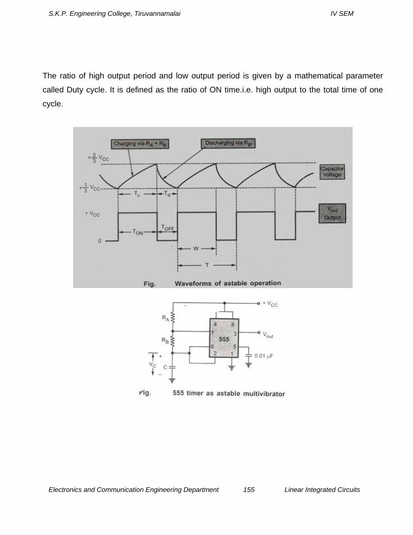
S.K.P. Engineering College, Tiruvannamalai IV SEM
Electronics and Communication Engineering Department 155 Linear Integrated Circuits
The ratio of high output period and low output period is given by a mathematical parameter
called Duty cycle. It is defined as the ratio of ON time.i.e. high output to the total time of one
cycle.

S.K.P. Engineering College, Tiruvannamalai IV SEM
Electronics and Communication Engineering Department 156 Linear Integrated Circuits
4. Explain Applications of astable multivibrator. [CO5- L3] Astable Multivibrator Applications: (a) Square wave oscillator:(Schmitt Trigger) With out reducing RA = 0 ohm, the astable multivibrator can be used to produce square
wave output. Simply by connecting diode D across Resistor RB. The capacitor C charges
through RA & diode D to approximately 2/3 Vcc & discharges through RB & Q1 until the
capacitor voltage equals approximately 1/3 Vcc, then the cycle repeats.
To obtain a square wave output, RA must be a combination of a fixed resistor &
potentiometer so that the potentiometer can be adjusted for the exact square wave.
(b) Free – running Ramp generator:
• The astable multivibrator can be used as a free – running ramp generator when resistor RA &
RB are replaced by a current mirror.
• The current mirror starts charging capacitor C toward Vcc at a constant rate.

S.K.P. Engineering College, Tiruvannamalai IV SEM
Electronics and Communication Engineering Department 157 Linear Integrated Circuits
• When voltage across C equals to 2/3 Vcc, upper comparator turns transistor Q1 ON & C
rapidly discharges through transistor Q1.
• When voltage across C equals to 1/3 Vcc, lower comparator switches transistor OFF & then
capacitor C starts charging up again..
• Thus the charge – discharge cycle keeps repeating.
• The discharging time of the capacitor is relatively negligible compared to its charging time.
• The time period of the ramp waveform is equal to the charging time & is approximately is
given by,
T = VccC/3IC ………………………… (1)
IC = (Vcc - VBE)/R = constant current
Therefore the free – running frequency of ramp generator is
f 0 = 3IC/ Vcc C

S.K.P. Engineering College, Tiruvannamalai IV SEM
Electronics and Communication Engineering Department 158 Linear Integrated Circuits
5..Draw the circuit using op-amp to generate triangular wave. Explain its operation.[CO5 – L3-May – 2011] TRIANGULAR WAVE GENERATOR Figure 7.10(a) shows the circuit of a triangular wave generator. It consists of two op-amps and
several passive components. The op-amp A1 forms a non-inverting comparator with
hysteresis, which is a Schmitt Trigger. The op-amp A2 forms an integrator which integrates the
output obtained from the Schmitt trigger. The op-amp A1 is a two level comparator whose
outputs are determined by ±Vsat. The square-wave output from A1 is applied to the (-)ve input
terminal of the op-amp A2. The output of A2 is a triangular wave, and it is fed back as an input
to the comparator A1 through a voltage divider network formed by R2 and R3.
Loop Analysis : Let us consider that the output v’0 of comparator A1 is +Vsat initially. The integrator integrates
+Vsat and produces a negative going ramp at its output as shown in Fig. 7.10 (b). Hence, the
voltages at the two ends of the voltage divider formed by R2 - R3 are +Vsat at the output of A3
and Vsat at the output of A2. At the instant t = T1, when the negative going ramp reaches a
value of Vramp, represented as point a in Fig.7.10 (b), the effective value at the point P
becomes slightly less than 0V. This switches the op-amp A1 to its negative saturation level –
Vsat.
With the output of A1 at Vsat the op-amp A2 starts integrating and increases its output in the
positive direction. At the instant t =T2 shown as point b in Fig.7.10 (b) the voltage at P
becomes just more than 0V. This switches the output of op-amp A1 from -Vsat to +Vsat. This
cycle repeats itself, and generates a triangular waveform. The frequency of the waveform is
determined by the RC value of the integrator formed by op-amp A2 and the saturation voltage
levels +/-Vsat. of comparator op-amp A1.

S.K.P. Engineering College, Tiruvannamalai IV SEM
Electronics and Communication Engineering Department 159 Linear Integrated Circuits
6.Draw the circuit using op-amp to generate sawtooth wave. Explain its operation.[CO5-L3-May 2016] SAWTOOTH WAVE GENERATOR The saw tooth wave refers to a waveform with its rise time being many times longer than the
corresponding fall time or fall time very longer as compared to the rise time. Triangular wave
generator can be modified to produce a saw tooth waveform.
The saw tooth wave generator circuit is shown in Fig. 7.12(a).The op-amp A1 functions as a
ramp generator and the op-amp A2 function as a comparator. The input reference signal Vi of
value less than zero is connected to the inverting input of the op-amp. Since Vi is negative,
the output of op-amp A1 can only ramp up. The rate of raise is given by
VOR/t=Vi/RiC The ramp voltage VOR is monitored by the comparator A2. The output VOR is connected to the
non-inverting terminal of op-amp A2, and a reference voltage set by a potentiometer Vref is
connected to the inverting input of comparator. When the capacitor C charges, and when the
voltage is VOR below Vref the output of comparator is negative. Then the transistors Q1 and Q2
do not conduct. The diodes D1 and D2 protect the transistors from excessive reverse bias
voltages.

S.K.P. Engineering College, Tiruvannamalai IV SEM
Electronics and Communication Engineering Department 160 Linear Integrated Circuits
When VOR rises and just exceeds Vref ,the output VOC of comparator goes to positive
saturation.This action forward biases the transistor Q2 into saturation.The saturated transistor
then acts as a switch across the capacitor C, which charges quickly making the output Voc
come down essentially to 0V.
The positive saturation Voc, of A2 also makes the transistor Q1 ON, and the Vref or negative
input of op-amp A2 drops to 0V. As the capacitor C discharges rapidly making V0R zero volts,
it drops below Vref. This causes the comparator output to becomes negatively saturated. This
action switches the transistor (22 OFF, and C begins charging linearly, and the cycle repeats.
The sawtooth output waveform is shown in fig. Fig shows the sawtooth waveform designing
method.The circuit can also be operates as a current-controlled sawtooth waveform generator
by applying an external control current sink Is at the (-) input terminal of op-amp A1 is shown in
fig. Then,
f=Is/CVref

S.K.P. Engineering College, Tiruvannamalai IV SEM
Electronics and Communication Engineering Department 161 Linear Integrated Circuits
Here, the op-amp A1 can preferably be a FET input op-amp with low bias current and good
slew rate.
7. Describe in detail the working principle of IC 8038 function generator.[CO5- L2-Dec – 2011] ICL8038 FUNCTION GENERATOR Function Generator ICL 8038 Function generators are designed to provide the basic
waveforms such as square wave, triangular wave and sine wave. They are also called as
waveform generators. The monolithic function generators provide these basic waveforms with
a minimum number of external components reducing complexity, but increasing the reliability
of the circuit. They find application in communication, telemetry, electronic music, and testing
and calibration in the laboratory. In function generators, VCO (voltage controlled oscillator)
generates the triangular and square waves. The triangular wave is passed through the on chip
wave shaper to generate a sine wave. The sawtooth and pulse waveforms are generated by

S.K.P. Engineering College, Tiruvannamalai IV SEM
Electronics and Communication Engineering Department 162 Linear Integrated Circuits
configuring the oscillator for a highly asymmetric duty cycle.
8. Explain in detail about features and internal structure of IC 723 with block diagram? [CO5 – L2-May 2016] General purpose linear IC723 regulator. The three terminal regulators discussed earlier have the following Iimtieee 1. Not short circuit
protection 2. Output voltage (positive or negative) is fixed. These limitations have been
overcome in the 723 general Purim. regulator, which can be adjusted over a wide range of
both positive or negative regulated voltage. This IC is inherently low current device, but can be
boosted to provide 5 amps or more current by connecting external components. The limitation
of 723 is that it has no in-built thermal protection. It also has no short circuit current limits.
Figure shows the functional block diagram of a 723 remdator IC. It has two separate sections.
The sever diode, a constant current source and reference amplifier produce a fixed voltage of
about 7 volts at the terminal V. The constant current source forces the goner to operate at a

S.K.P. Engineering College, Tiruvannamalai IV SEM
Electronics and Communication Engineering Department 163 Linear Integrated Circuits
fixed point so that the sever outputs a fixed voltage. The other eection of the IC consists of en
error amplifier, a series pass transistor Q, and a current limit transistor Q2. The error amplifier
compares a sample of the output voltage applied at the INV input terminal to the reference
voltage Vy applied at the NI input terminal.
Functional block diagram IC 723 regulator:
Output voltage is compared with this temperature compensated reference potential of the
order of 7 volts. For this, Vrd is connected to the non-inverting input of the error amplifier. This
error amplifier is high gain differential amplifier. It's inverting input is connected to the either
whole regulated output voltage or part of that from outside. For later case a potential divider of
two scaling resistors is used. Scaling resistors help in getting multiplied reference voltage or
scaled up reference voltage. Error amplifier controls the series pass transistor Qt, which acts
as variable resistor. The series pass transistor is a small power transistor having about 800
mW dissipation. The unregulated power supply source (< 36V d.c.) is connected to collector of
series pass transistor.
Transistor Q2 acts as current limiter in case of short circuit condition. It senses drop across lcc
placed in series with regulated output voltage externally. The frequency compensation terminal
controls the frequency response of the error amplifier. The required roll-off is obtained by

S.K.P. Engineering College, Tiruvannamalai IV SEM
Electronics and Communication Engineering Department 164 Linear Integrated Circuits
connecting a small capacitor of 100 pF between frequency compensation and inverting input
terminals.
Important Features of IC 723 1) It works as voltage regulator at output voltage ranging from 2 to 37 volts at currents upto
150 mA.
2) It can be used at load currents greater than 150 mA with use of suitable NPN or PNP
external pass transistors.
3) Input and output short-circuit protection is provided.
4) It has good line and load regulation (0.03%)
5) Wide variety of applications of series, shunt, switching and floating regulator.
6) Low temperature drift and high ripple rejection.
7) Low standby current drain.
8) Small size, lower cost
9) Relative ease with which power supply can be designed.
10) Provides a choice of supply voltage.
9. State the limitiations of linear voltage regulators. [CO5- L2] Linear regulated power supplies have following limitations :
1) The required input step down transformer is bulky and expensive.
2) Due to low line frequency (50 Hz), large values of filter capacitors are required.
3) The efficiency is very low.
4) Input must be greater than the output voltage.
5) As large is the difference between input and output voltage, more is the power dissipation in
the series pass transistor.
6) For higher input voltages, efficiency decreases.
7) The need for dual supply, is not economical and feasible to achieve with the help of linear
regulators. The switching regulators overcome all these limitations.

S.K.P. Engineering College, Tiruvannamalai IV SEM
Electronics and Communication Engineering Department 165 Linear Integrated Circuits
10.Explain the working of step-down switching regulator.[CO5 – L2 -May – 2011] BUCKING SWITCHING REGULATOR Figure 8.28 shows the basic diagram of a step-down or bucking switching s base to regulator
circuit. The input voltage Vi is a dc voltage. A pulse train is applied efficiently to the base of the
control transistor Q1, and the transistor acts as a switch, alternating between its cut-off and
saturation regions. When the transistor is ON, the diode D gets reverse biased. When the
transistor is OFF, it becomes forward biased providing a continuous path for the inductive
current. The LC filter functions as a smoothing circuit for the input variations that provides , a
steady dc output voltage.
When the transistor Q1 is turned ON and OFF for equal time durations, i.e. when duty cycler D
of the pulse train is 50%, the dc output voltage V0 is The given by V0 = (tON /T)Vi =0.5Vi. Note
that the voltage drop across transistor and diodes are neglected. A typical switching frequency
for the transistor is several kHz.
The reference voltage Vref is obtained from the unregulated input voltage with the use of a
Zener diode. The error circuit compares the regulated output voltage with the Vref voltage. The
output of the error circuit operates the pulse width modulator. The pulse width modulator
generates pulses at a fixed t frequency width of the pulses is dependent on the control voltage
from the error circuit. When the dc output voltage falls below the reference voltage, the error
signal is generated in the error circuit.This causes the width of the pulses to increase ,thus
increasing the output voltage.If the output voltage is more than the reference voltage ,error
signal reduces the pulse width which results in reducing the output voltage.Thus the constant
output voltage is maintained.

S.K.P. Engineering College, Tiruvannamalai IV SEM
Electronics and Communication Engineering Department 166 Linear Integrated Circuits
11.With suitable diagram, explain the working of a switched capacitor filter. Also explain how resistor can be realized using switched capacitor filter. [CO5- L3 -May – 2011] SWITCHED CAPACITOR FILTER Active RC filters using ICs have advantages of not using inductors and of offering easy
implementation of various high performance low-pass, high-pass, band-pass and band-
elimination filters. The resistor values needed for these filters are generally much too large for
fabrication on a monolithic IC chip. Integrated (diffused) resistors have poor temperature and
linearity characteristics. Large value resistors (≥10 kΩ) take up an excessive amount of chip
area. This is the major reason that active filters have not previously been fully integrated in
MOS technology. The switched capacitor filter offers an attractive alternative to the
conventional RC active filter.
A switched capacitor filter shown in Fig. is a three terminal element which consists of
capacitors, periodic switches and operational amplifiers and whose open circuit voltage
transfer function represents filtering characteristics. It is not possible to manufacture passive
elements of an RC active filter with suitable values and quality in the same technology as the
op-amps. For the range of frequencies within which the op-amp operates satisfactorily, it is not
possible in MOS technology to implement RC products of sufficient magnitude and accuracy.

S.K.P. Engineering College, Tiruvannamalai IV SEM
Electronics and Communication Engineering Department 167 Linear Integrated Circuits
On the other hand, in the case of switched capacitor filter, the RC products are set by
capacitor ratios and the switch period. In MOS technology, the accuracy and the values of
these quantities are suitable for the implementation of selective filters. The large resistor
values required for active Alter are easily simulated by the combination of small value
capacitors (say 10 PF) and MOS switching transistors. The equivalent resistor value so
obtained is high enough such that the filter capacitance value should be small enough to be
easily incorporated on a monolithic IC chip.

S.K.P. Engineering College, Tiruvannamalai IV SEM
Electronics and Communication Engineering Department 168 Linear Integrated Circuits
12. With a neat functional diagram explain the operation of LM 380 power amplifier.[CO5- L3 –May/June2016]
LM 380 is a popular power audio amplifier produced by national semiconductor. It is capable of
delivering 2.5 W minimum to 8Q load. Hence it is very much ideal for consumer applications.
Features of LM380:
• Internally fixed gain of 50 (34dB)
• Output is automatically self centering to one half of the supply voltage.
• Output is short circuit proof with internal thermal limiting.
• Input stage allows the input to be ground referenced or ac coupled.
• Wide supply voltage range (5 to 22V).
• High peak current capability.
• High impedance.
• Low total harmonic distortion
• Bandwidth of 100KHz at Pout = 2W & RL = 8Ω Pin diagram of LM380: The figure shows the pin diagram of LM380 power audio amplifier. A copper lead frame is
used with the center three pins on either side (3,4,5,10,11,12) of DIP package comprises a
heat sink.

S.K.P. Engineering College, Tiruvannamalai IV SEM
Electronics and Communication Engineering Department 169 Linear Integrated Circuits
Fig: Pin diagram
(i) PNP Emitter follower:
• The input stage is emitter follower composed of PNP transistors Q1 & Q2 which
drives the PNP Q3-Q4 differential pair.

S.K.P. Engineering College, Tiruvannamalai IV SEM
Electronics and Communication Engineering Department 170 Linear Integrated Circuits
• The choice of PNP input transistors Q1 & Q2 allows the input to be referenced to
ground i.e., the input can be direct coupled to either the inverting & non-inverting
terminals of the amplifier.
(ii) Differential Amplifier:
• The current in the PNP differential pair Q3-Q4 is established by Q7, R3 & +V.
• The current mirror formed by transistor Q7, Q8 & associated resistors then
establishes the collector current of Q9.
• Transistor Q5 & Q6 constitute of collector loads for the PNP differential pair.
• The output of the differential amplifier is taken at the junction of Q4 & Q6 transistors &
is applied as an input to the common emitter voltage gain.
(iii) Common Emitter:
• Common Emitter amplifier stage is formed by transistor Q9 with D1, D2 & Q8 as a
current source load.
• The capacitor C between the base & collector of Q9 provides internal compensation &
helps to establish the upper cutoff frequency of 100 KHz.
• Since Q7 & Q8 form a current mirror, the current through D1 & D2 is approximately
the same as the current through R3.
• D1 & D2 are temperature compensating diodes for transistors Q10 & Q11 in that D1
& D2 have the same characteristics as the base-emitter junctions of Q11. Therefore
the current through Q10 & (Q11-Q12) is approximately equal to the current through
diodes D1 & D2.

S.K.P. Engineering College, Tiruvannamalai IV SEM
Electronics and Communication Engineering Department 171 Linear Integrated Circuits
(iv) (Output stage) - Emitter follower: Emitter follower formed by NPN transistor Q10 & Q11. The combination of PNP transistor Q11
& NPN transistor Q12 has the power capability of an NPN transistors but the characteristics of
a PNP transistor.
• The negative dc feedback applied through R5 balances the differential amplifier so that the
dc output voltage is stabilized at +V/2;
• To decouple the input stage from the supply voltage +V, by pass capacitor in order of micro
farad should be connected between the by pass terminal (pin 1) & ground (pin 7).
• The overall internal gain of the amplifier is fixed at 50. However gain can be increased by
using positive feedback.

S.K.P. Engineering College, Tiruvannamalai IV SEM
Electronics and Communication Engineering Department 172 Linear Integrated Circuits
13.A 555 timer is configured in astable mode with RA =2 kohm RB =6kohm and C=0.1uF.Determine the frequency of oscillation.[CO5 –H3 –May/June 2016] T=0.69(RA+2RB)C
So,
f=1/T=1.45/[( RA+2RB)C]
f=1.45/[(2k+12k)0.1u]
f=1.035Kohm.