slurry chemistry effects on copper chemical mechanical
TRANSCRIPT

University of Central Florida University of Central Florida
STARS STARS
Electronic Theses and Dissertations, 2004-2019
2004
Slurry Chemistry Effects On Copper Chemical Mechanical Slurry Chemistry Effects On Copper Chemical Mechanical
Planarization Planarization
Ying Luo University of Central Florida
Part of the Engineering Commons
Find similar works at: https://stars.library.ucf.edu/etd
University of Central Florida Libraries http://library.ucf.edu
This Masters Thesis (Open Access) is brought to you for free and open access by STARS. It has been accepted for
inclusion in Electronic Theses and Dissertations, 2004-2019 by an authorized administrator of STARS. For more
information, please contact [email protected].
STARS Citation STARS Citation Luo, Ying, "Slurry Chemistry Effects On Copper Chemical Mechanical Planarization" (2004). Electronic Theses and Dissertations, 2004-2019. 36. https://stars.library.ucf.edu/etd/36

SLURRY CHEMISTRY EFFECTS ON COPPER CHEMICAL MECHANICAL PLANARIZATION
by
YING LUO B.S. Beijing University of Aeronautics and Astronautics, 1994
A thesis submitted in partial fulfillment of the requirements for the degree of Master of Science
in the Department of Mechanical, Materials, and Aerospace Engineering in the College of Engineering and Computer Science
at the University of Central Florida Orlando, Florida
Summer Term 2004

ABSTRACT
Chemical-mechanical Planarization (CMP) has emerged as one of the fastest-growing
processes in the semiconductor manufacturing industry, and it is expected to show equally
explosive growth in the future (Braun, 2001). The development of CMP has been fueled by the
introduction of copper interconnects in microelectronic devices. Other novel applications of CMP
include the fabrications of microelectromechanical systems (MEMS), advanced displays, three
dimensional systems, and so on (Evans, 2002). CMP is expected to play a key role in the next-
generation micro- and nanofabrication technologies (Singh, et al., 2002).
Despite the rapid increase in CMP applications, the fundamental understanding of the
CMP process has been lacking, particularly the understanding of the wafer-slurry-pad interactions
that occur during the CMP process. Novel applications of CMP are expected to expand to
materials that are complex chemically and fragile mechanically. Thus, fundamental understanding
and improvement of slurry design for CMP is the key to the development of sophisticated next-
generation CMP processes.
Slurry performance for CMP can be determined by several output parameters including
removal rate, global planarity, surface topography, and surface defectivity. To achieve global
planarity, it is essential to form a very thin passivating surface layer (<2 nm) that is subsequently
removed by the mechanical component of the slurry (Kaufman et al., 1991) or by combined
chemo-mechanical effects (Tamboli, 2000). Chemical additives like hydrogen peroxide (H2O2),
potassium ferricyanide, and ferric chloride are added to slurries as oxidizers in order to form a
ii

desirable surface layer. Other chemical additives such as inhibitors (e.g. benzotriazole) and
complexing agents (e.g. ammonia) are added to the copper slurry in order to modify the oxide
layer. That the removal rate of the thin surface layer is greater at the highest regions of the wafer
surface than at the lowest regions leads to surface planarity.
In this study, various complexing agents and inhibitors are combined to form slurry
chemistry for copper CMP processing in H2O2 based slurries at pH values ranging from 2 to 10.
Two complexing agents (glycine and Ethylenediamine) and one inhibitor (3-amino-1, 2, 4-
triazole) were selected as slurry constituents for detailed chemical synergistic effect study
because they showed good materials removal and surface planarity performances.
To understand the fundamental mechanisms involved in copper CMP process with the
afore-mentioned slurry chemical formations, various techniques, such as electrochemical testing
techniques (including potentiodynamic polarization and electrochemical impedance
spectroscopy), x-ray photoelectron spectroscopy (XPS), atomic force microscopy (AFM), and
scanning electron microscopy (SEM), were applied. As a result, guidelines for optimized slurry
chemical formulation were arrived at and the possible mechanisms of surface-chemical-abrasive
interactions were determined. From applications point of view, this study serves as a guide for
further investigations in pursuing highly effective slurry formulations for copper/low-k
interconnect applications.
iii

ACKNOWLEDGEMENTS
I take this opportunity to thank my advisor Dr. Vimal Desai. He has always been giving
timely support and encouragement to me with his vision and insights. He has been taking efforts
to expose students to industrial interactions and international conferences, which helped me
shaping this thesis and enhancing my professional growth tremendously. I benefited a lot from
him both professionally and personally. It is an honor to be his graduate student.
I thank Dr. Sudipta Seal for agreeing to be in my thesis committee and his general
interest in my work. I am also thankful to Dr. Kalpathy Sundaram for his advice and
encouragement over my two-years’ research. I would like to thank Dr. Dnyanesh Tamboli for
serving on my thesis committee and bringing industrial perspective. His comments and
suggestions helped me to put my graduate research right on track.
I am grateful to Dr. Tianbao Du for his guidance and help with all aspects of my thesis
from the experimentation and analysis to the defense. His timely advises and suggestions put me
in the right perspective during tough times. This thesis cannot have been completed without his
input. I thank Arun Vijayakumar for his help during my research and graduate studies. And I
thank everyone at AMPAC who has done me favors, small or large.
At last but not least, I thank my family and friends for their love and support.
iv

TABLE OF CONTENTS
LIST OF FIGURES ..................................................................................................................... viii
LIST OF TABLES........................................................................................................................ xii
CHAPTER ONE : INTRODUCTION.............................................................................................1
1.1 Overview............................................................................................................................... 1
1.1.1 Chemical Mechanical Planarization ............................................................................. 1
1.1.2 Applications of CMP Process ....................................................................................... 3
1.1.3 Advantages in CMP ...................................................................................................... 5
1.1.4 Alternatives to CMP ..................................................................................................... 6
1.2 Evolution of CMP in copper interconnect ............................................................................ 8
1.2.1 Copper replace Aluminum as wiring material .............................................................. 8
1.2.2 Damascene technology with Cu CMP .......................................................................... 9
1.2.3 Cu and barrier layer CMP........................................................................................... 11
1.2.4 CMP in Copper/Low-k Dielectric Integration Schemes............................................. 12
1.3 Challenges for Cu CMP...................................................................................................... 14
1.4 Objective of this study ........................................................................................................ 18
CHAPTER TWO : LITERATURE REVIEW...............................................................................21
2.1 Mechanical concepts of CMP process ................................................................................ 21
2.1.1 Pad-slurry-wafer interaction ....................................................................................... 21
2.1.2 Mechanical modeling for CMP process design .......................................................... 24
v

2.2 Electrochemical Phenomena............................................................................................... 27
2.2.1 surface film formation................................................................................................. 27
2.2.2 The effect of complexing agent .................................................................................. 30
2.2.3 Inhibitors ..................................................................................................................... 33
2.3 Copper CMP integration and manufacturability................................................................. 34
2.3.1 Dishing and Erosion.................................................................................................... 34
2.3.2 Post-CMP cleaning ..................................................................................................... 38
CHAPTER THREE : EXPEREMENTAL.....................................................................................41
3.1 Chemical Mechanical Polishing & static etching ............................................................... 41
3.2 Electrochemical testing....................................................................................................... 43
3.2.1 Potentiodynamic polarization ..................................................................................... 43
3.2.2 Electrochemical Impedance Spectroscopy (EIS)........................................................ 47
3.3 Surface Characterization............................................................................................... 50
3.3.1 Surface topography: Atomic Force Microscopy......................................................... 50
3.3.2 Scanning Electron Microscope (SEM) ....................................................................... 51
3.3.3 X-ray Photoelectron Spectroscopy (XPS) .................................................................. 51
CHAPTER FOUR : RESULTS AND DISCUSSION...................................................................53
4.1 Removal rate, etching rate, and surface finish.................................................................... 53
4.1.1 Removal rate vs. etching rate...................................................................................... 53
4.1.2 Copper disk vs. thin film............................................................................................. 59
4.1.3 Glycine vs. EDA as complexing agent ....................................................................... 62
vi

4.2 Electrochemical investigations ........................................................................................... 65
4.2.1 Cu-H2O2-glycine system............................................................................................. 65
4.2.2 Cu-H2O2-glycine-ATA system ................................................................................... 68
4.2.2 Cu-H2O2-EDA-ATA system....................................................................................... 73
4.3 Surface analysis .................................................................................................................. 77
4.3.1 XPS analysis ............................................................................................................... 77
4.3.2 SEM analysis .............................................................................................................. 84
4.3.3 AFM images................................................................................................................ 88
CHAPTER FIVE : SUMMARY....................................................................................................92
LIST OF REFERENCES...............................................................................................................95
vii

LIST OF FIGURES
Figure 1.1 A schematic setup for standard CMP processing. ..........................................................2
Figure 1.2 Examples of ILD CMP, STI CMP, and Metal CMP processing....................................3
Figure 1.3 Process steps to fabricate a dual damascene structure with copper and ILD (which
is low-k material in this case). SiN and low-k dielectric deposition; via definition by
etch; pad definition by etch; barrier (e.g., tantalum) seed (Cu) physical vapor deposition;
and copper electroplating and chemical-mechanical polishing. (Hu et al., 1998) .................10
Figure 1.4 Schematic detaining typical multi-step CMP process sequence for polishing of
Cu/low-k interconnects (Lee et al., 2003)..............................................................................12
Figure 1.5 ITRS 2002 Projections for future technology nodes and year of production for a)
intermediate wiring pitch (solid bars) and allowable copper thinning at minimum pitch
due to erosion (diamond symbols), and b) number of metal layers (square symbols) and
target bulk dielectric constant (diamond symbols) of inter-level dielectric...........................15
Figure 1.6 Schematic of damascene Cu/low-k interconnect structure identifying specific
integration concerns for CMP (Lee et al, 2003).....................................................................18
Figure 2.1 Schematic diagram depicting (a) microscale and (b) nanoscale phenomena that
occur during CMP..................................................................................................................22
Figure 3.1 Schematic of a polarization diagram observed typically for materials exhibiting
passivation behavior...............................................................................................................45
Figure 3.2 Impedance network model for a metal in electrolyte (MacDonald, 1987)...................49
viii

Figure 4.1 Removal rate behavior of Cu in H2O2 based slurries with different combinations
of complexing agents and inhibitors at various pH values. ...................................................54
Figure 4.2. Removal rate vs. etching rate of copper disk in H2O2 based slurries/solutions with
citric acid plus ATA or thiourea at pH 2, 4, 6, and 10...........................................................56
Figure 4.3 Removal rate vs. etching rate of copper disk for glycine/EDA with or without
ATA as inhibitor in H2O2 based slurries/solutions at pH 2, 4, 6, 10. ....................................57
Figure 4.4 Rate ratio (Removal rate to etching rate) for copper with different combinations of
complexing agents and inhibitors in H2O2 based slurries/solutions at pH 2, 4, 6, 10............58
Figure 4.5 Removal rate data of copper disk and thin film for four different slurry chemistries
in H2O2 based slurries. ...........................................................................................................60
Figure 4.6 Surface roughness of copper disks and thin films after CMP in H2O2 based slurries
with different slurry chemistry...............................................................................................61
Figure 4.7 Removal rate data for copper disk CMP in H2O2 based slurries at pH values of 2,
4, 6 and 10. (a). Removal rates in slurries without additives, with glycine, and with
glycine+ATA. (b). Removal rates in slurries without additives, with EDA, and with
EDA+ATA.............................................................................................................................64
Figure 4.8 Potentialdynamic polarization curves for copper surface immersed in H2O2 based
solutions containing glycine at various pH values.................................................................66
Figure 4.9 Potential-pH diagram for Cu-glycine system. ..............................................................67
Figure 4.10 Variation of Icorr values of copper surface in H2O2 based solutions with and
without 0.01M glycine at various pH values. ........................................................................67
ix

Figure 4.11 Removal rate vs. etch rate data for copper in H2O2 based slurries/solutions
without glycine, with glycine, and with glycine plus ATA at pH 10. ...................................69
Figure 4.12 Potentialdynamic scan for copper surface immersed in H2O2 based solutions
without glycine, with glycine, and with glycine plus ATA at pH 10. ...................................70
Figure 4.13 EIS Nyquist plot for copper surface immersed in H2O2 based solutions without
glycine, with glycine, and with glycine plus ATA at pH 10..................................................72
Figure 4.14 Removal rate vs. etching rate data for the Cu-H2O2-EDA-ATA system at various
pHs. ........................................................................................................................................74
Figure 4.15 Potentialdynamic scan for copper surface immersed in H2O2 based solutions with
EDA plus ATA at pH 2, 4, 6, and 10. ....................................................................................74
Figure 4.16 Corrosion potential and corrosion current density data derived from Fig. 4.15........75
Figure 4.17 EIS Nyquist plot for copper surface immersed in H2O2 based solutions with EDA
plus ATA at pH 2, 4, 6, and 10. .............................................................................................76
Figure 4.18 Equivalent circuit used for fitting EIS Nyquist plot shown in Fig 4.17. ....................76
Figure 4.19 Cu (2p3/2) XPS of copper oxide films formed in solutions with 5% H2O2 at
different pH after 10 minutes of immersion at (a) pH 2 (b) pH 4 (c) pH 6 and (d) pH
10............................................................................................................................................78
Figure 4.20 XPS Cu LMM Auger lines of copper oxide films formed in solution with 5%
H2O2 at different pH after 10 minutes of immersion. at (a) pH2, (b) pH4, (c) pH6, and
(d) pH10. ................................................................................................................................80
x

Figure 4.21 Cu (2p3/2) XPS of copper oxide films formed in solutions with 5% H2O2 and
0.01M glycine at different pH after 10 minutes of immersion at (a) pH2, (b) pH4,
(c)pH6, and (d) pH10. ...........................................................................................................80
Figure 4.22 Cu (2p3/2) XPS of copper oxide films formed in solutions with 5% H2O2, 0.01M
glycine and 0.1wt% ATA after 10-minute immersion at (a) pH2, (b) pH6, (c)pH4, and (d)
pH10.......................................................................................................................................82
Figure 4.23 XPS N(1s) spectra of Cu surface after 10 minute immersion in H2O2 based
solutions at pH10 containing (a) 0.01M glycine and (b) 0.01M glycine and 0.1wt%
ATA. ......................................................................................................................................83
Figure 4.24 SEM images of copper surface after 60-minute immersion in H2O2 based
solutions at (a) pH2, (b) pH4, (c) pH6, and (d) pH10............................................................86
Figure 4.25 SEM images of copper surface after 60-minute immersion in H2O2 based
solutions at pH10 with (a) 0.01M glycine (b) 0.01M glycine and 0.1wt% ATA. ................88
Figure 4.26 AFM images of copper surface after CMP in H2O2 based slurries at pH10 in
conditions of (a) without chemical additives, (b) with 0.01M glycine (c) with 0.01 M
glycine and 0.1wt% ATA, and (d) with 0.01 M EDA plus 0.1wt% ATA. ............................91
xi

LIST OF TABLES
Table 1.1 Materials to be Polished and Possible Applications (Steigerwarld et al. 1997) ............. 4
Table 1.2 Degrees of Planarity (Sivaram et al. 1991)..................................................................... 5
Table 1.3 Guiding principles for slurry design in CMP (adapted from singh et al, 2002) ........... 16
Table 4.1 Combinations of complexing agents and inhibitors in removal rate study of copper
CMP in H2O2 based slurries at pH2, 4, 6 and 10................................................................. 55
Table 4.2 Removal rate data for 6 combinations of complexants and inhibitors in H2O2 based
slurries at pH value of 2, 4, 6 and 10. ................................................................................... 59
Table 4.3 Corrosion potential and corrosion current density data derived from Fig. 4.12........... 70
Table 4.4 Rp values for Cu-H2O2-EDA-ATA system at different pH values. ............................. 77
xii

CHAPTER ONE : INTRODUCTION
1.1 Overview
1.1.1 Chemical Mechanical Planarization
Chemical mechanical planarization (CMP) is a process to planarize metal and dielectric
surfaces typically in microelectronic devices by combining chemical and mechanical
interactions. Here the term planarization is used instead of polishing because after CMP, we
expect the surface to be polished smooth and planarized as well. In terms of planarization, there
is local or global planarization respectively. The uniqueness of CMP is that it achieves global
planarization which is essential for multilevel interconnect fabrications.
There are three main components in the CMP process: the surface to be polished, the pad,
and the slurry. In CMP processing, a down force is applied to the sample surface against a
rotating pad. The slurry containing submicron-sized abrasives and chemicals flows between the
sample surface and the pad for material removal by mechanical and chemical action. That the
materials in higher regions are removed faster than those in lower regions leads to planarization.
The planarization ability of a CMP process is measured by the planarization rate defined by
Equation 1.1 (Steigerwarld et al., 1997).
Planarization rate = polish rate of the high features – polish rate of the low features 1.1
1

In a typical CMP process, as shown schematically in Fig.1.1, there are over 20 input
variables that affect the output variables (>4) like removal rate and surface quality (Steigerwarld
et al., 1997). Most input variables are related to the sample surface (i.e. wafer structure, wafer
pattern geometry), the pad (i.e. pad structure and mechanical properties, pad rotating rate), and
the slurry (i.e. slurry chemistry, slurry flow rate). Temperature, pressure, and post CMP cleaning
are other critical input parameters for CMP process integration.
Figure 1.1 A schematic setup for standard CMP processing.
To improve planarization, it is needed to minimize the pressure, maximize the platen
speed and use slurry chemistry that does not remove material without abrasion. Meantime, high
removal rate and removal rate uniformity across a wafer are wanted to improve throughput. Both
of these are also strong functions of down force, platen speed, pad structure, and slurry
chemistry. Usually, the goals for maximum removal rate and optimized planarization are
2
conflicting with each other. Thus, the CMP process is tailored for various applications and
priority of responses.
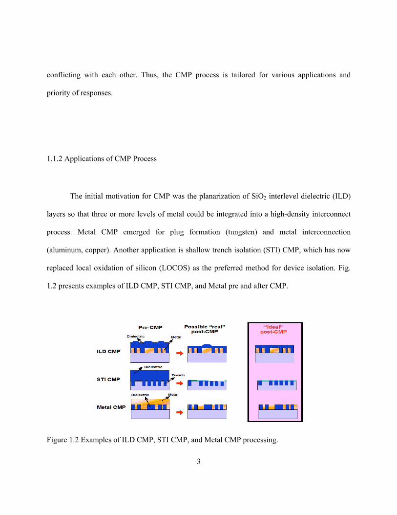
1.1.2 Applications of CMP Process
The initial motivation for CMP was the planarization of SiO2 interlevel dielectric (ILD)
layers so that three or more levels of metal could be integrated into a high-density interconnect
process. Metal CMP emerged for plug formation (tungsten) and metal interconnection
(aluminum, copper). Another application is shallow trench isolation (STI) CMP, which has now
replaced local oxidation of silicon (LOCOS) as the preferred method for device isolation. Fig.
1.2 presents examples of ILD CMP, STI CMP, and Metal pre and after CMP.
Figure 1.2 Examples of ILD CMP, STI CMP, and Metal CMP processing.
3

In addition to purely conventional electronic applications, substantial efforts are being put
forth to adapt the CMP process to the formation of gate electrodes for high-k dielectrics, gate
structures and interconnect technology for ferroelectric and ferromagnetic nonvolatile memories,
STI applications in high-speed Si-Ge devices, planarization of multidimentional MEMS,
fabrication of three-dimensional memories and optical-bandgap materials, and planarization of
III-V and other semiconductor substrates (Aluminum nitride, gallium nitride, silicon carbide,
diamond, etc.) for high-quality epitaxial growth (Singh, et al., 2002). Table 1.1 gives a detailed
description of the current and future materials and application choices for CMP.
Table 1.1 Materials to be Polished and Possible Applications (Steigerwarld et al., 1997)
Materials Application Metal Al, Cu, Cu-Alloys, Al-Alloys Interconnection
Ta/TaN, Ti/TiN, TiNxCy WSix, W-Si-N, TaSix, Ta-Si-N
Diffusion Barrier/Adhesion Promoter (DB/AP) Diffusion Barrier/Adhesion Promoter (DB/AP)
W Interconnection/e-Emitter NiFe Electromagnetic devices Dielectric Polysilicon Gate/Interconnection SiO2 Shallow Trench Isolation (STI)
SiO2, BPSG, PSG, Polymer Porous MSQ/HSQ, Porous SiOC Porous Organic Polymer
Interlayer Dielectric (ILD) Low-k ILD Low-k ILD
Si3N4 or SiOxNy Passivation/Hard CMP/ Stop Layer Other Aerogels ILD ITO Flat Panel High K Dielectrics Packaging/Capacitor High Tc Superconductor Interconnection/Packaging Optoelectronic Materials Optoelectronics Plastics, Ceramic Packaging
Silicon-on-Insulator (SOI) Si-Ge
Advanced Devices/Circuits Advanced Devices/Circuits
4
1.1.3 Advantages of CMP
Before the emergence of the CMP process, several methods were used for smoothing and
planarization, such as reactive ion etching (RIE)/sputter etching (Olsen et al., 1993), biased
electron cyclotron resonance (ECR) plasma deposition (Olsen et al., 1993), and spin on glasses
(SOG) (Chu et al., 1987). Basically, all those methods deliver either local planarization and/or
surface smoothing.
The primary advantage of CMP is that it achieves global planarity. The quantitative
features of global planarity verses local planarization and surface smoothing are listed in table
1.2. The planarization relaxation distance is defined as R, the distance traveled over a step,
whereupon the original step height, topography, or depth of field, T, returns (Sivaram, et al.,
1991). The planarization angle θ is given by arctan(T/R).
Table 1.2 Degrees of Planarity (Sivaram et al. 1991)
Planarity R (µm)
Surface Smoothing 0.1-2.0 >30
Local Planarization 2.0-100 30-0.5
Global planarization ≥100 ≤0.5
5
The advantage of global planarity enables the CMP process to meet deep sub-micron
focal depth requirements, to be applicable to more aggressive design rules, and to satisfy new
structure engineering needs. Besides, CMP yields improved metal step coverage. Another
advantage related to global planarization is that all types of surfaces (even multi-materials
surfaces) can be planarized by CMP due to its high degree of process flexibility, particularly in
the chemical formulations of polishing solutions and slurries (Evans, 2002).
Additionally, CMP has several cost advantages such as decreased processing complexity
and practical reduction in nonplanarity defects (metal stringers and lower defect densities). These
features translate to cost reduction, increased die yield, and decreased die cost. Generally, CMP
offers increased reliability, speed and yield of sub-0.5 µm devices and circuits (Steigerwarld et
al., 1997).
1.1.4 Alternatives to CMP
From a forward-looking perspective, there are several developing alternatives or
competing process to traditional CMP process, such as chemically-enhanced CMP, abrasive free
polishing (AFP), spin etch, planar etch, electropolishing, etc.
Chemically-enhanced planarization (CEP) uses controlled chemical etching of metals to
planarize. The CEP technique can employ electrochemical and diffusion controlled chemical
reactions for copper planarization (Lee et al., 2003).
6

Fixed-abrasive processing and abrasive free polishing (AFP) are derivatives of CMP
process. They are supposed to be cleaner processes resulting in smoother surface with less
dishing and within wafer non-uniformity (WIWNU) because slurry particles do not penetrate the
features (Evans, 2002).
In the spin-etch planarization (SEP) process, the chemical removal of copper films is
controlled by dispensing a reactive etchant solution on the substrate’s surface while it is spinning
(Fury et al., 1999). SEP is a polishing process with no mechanical force involved, which might
be applied for low-k dielectrics.
Planar etch, with contact planarization as an example, is also currently being explored.
Contact planarization is a method that uses a flat optical lens to flatten a sacrificial layer over the
dielectric layer, which is then cured with ultraviolet light and etched away before the final etch.
Electropolishing is being developed to open up wider choices for low-k dielectric
materials because the main feature of electropolishing is stress free. Therefore, softer dielectric
materials, such as spin-on, porous Xerogel materials with low-k dielectric ratings from 2.5 to 1.5,
become viable candidates for copper interconnection.
7

1.2 Evolution of CMP in copper interconnect
1.2.1 Copper replace Aluminum as wiring material
Aluminum-based alloys were the standard wiring material used in the semiconductor
industry. The integrated circuit (IC) development requires the average width of interconnects to
decrease to provide smaller dimensions, which are needed to pack in more transistors and more
wires. For example, ultra large scale integrated (ULSI) circuit technology at 0.18 µm (180 nm)
design rules will incorporate more than 10 million transistors on a single chip and 50 million
connections. As a result, average interconnect resistance is increasing. The speed at which a
signal can propagate down a wire is proportional to the product of the wire resistance (R) and the
wire capacitance (C). This speed is known as the wire’s RC delay as described in equation 1.2
(Wilson et al., 1993):
tdlRC
2
ρε= 1.2
Increased wire resistance, or capacitance, results in increased RC delay and slower signal
propagation. Whereas metal-oxide semiconductor (MOS) transistors tend to get faster with each
new generation, interconnects tend to get slower. In newer technologies, RC delay is increasing
while clock cycle time is decreasing; therefore, interconnect delay is now a significant fraction of
clock cycle time.
One way to meet the challenge of improving both the density and the performance of
interconnect is to add more layers of interconnects. IC process technologists now spend as much
8

effort developing advanced interconnects as they do developing transistors. And the process
steps involved in forming the interconnect represent about 50% of total wafer process cost.
Copper, with a resistivity of 1.7 µΩ-cm, is replacing Aluminum alloys with a resistivity
of 3 µΩ-cm, for interconnect wiring. Copper has almost two fold reduction in resistivity relative
to aluminum alloys, which means an almost two fold improvement in interconnect RC delay. As
the minimum feature size of microelectronic devices reaches beyond the 130nm technology
node, copper has become the critical interconnect wiring material for interconnect technologies
of advanced microelectronic devices due to better electrical conductivity as well as improved
electromigration resistance (Nitta et al., 1993) (on the order of 10 times better as compared to
aluminum alloys).
1.2.2 Damascene technology with Cu CMP
For multi-level metallization (MLM), there are difficulties in copper patterning. Wet
etching cannot be used for patterning sub-micron structures due to its isotropic nature. RIE is
also not practical because volatile copper’s compounds at low temperature are lacking. The
availability of CMP offers a new way of making metal wires on a chip, which is named
damascene technique (Lakshminarayanan et al., 1994), instead of subtractive metallization
schemes.
9

Damascene process flows as shown in Fig. 1.3: The insulating material or interlayer
dielectrics (ILD) is etched anisotropically, creating grooves that are filled by electroplating of
copper. The conditions of electroplating are chosen such that the grooves are completely filled.
The excess metal on top of the dielectric material is removed by CMP. Dual-damascene (DD)
technique enables the formation of wires and vias in the same process step. At present, dual-
damascene is exclusively utilized in MLM. CMP is an enabling process step for a successful Cu
damascene process and the pervasive technology for copper metallization.
Figure 1.3 Process steps to fabricate a dual damascene structure with copper and ILD (which is low-k material in this case). SiN and low-k dielectric deposition; via definition by etch; pad definition by etch; barrier (e.g., tantalum) seed (Cu) physical vapor deposition; and copper electroplating and chemical-mechanical polishing. (Adapted from Hu et al., 1998)
10

1.2.3 Cu and barrier layer CMP
One major problem about metallization of Cu is that copper tends to diffuse rapidly
through silicon and silicon dioxide, which can cause leakage problems. Therefore, thin barrier
layers are employed in the Cu damascene process. Complex structures and multilayer stacks will
require planarization of up to four different materials, including copper and the barrier layer (e.g.
Ta/TaN), with all of the materials exhibiting different polish rates. Therefore, a typical multi-step
CMP is the dominant approach used today. The first step in the CMP process is to remove the
bulk of copper, and stop at the underlying diffusion barrier. At this point, a suitable slurry is
utilized to polish the remaining copper and the barrier metal. The final step involves buffing,
cleaning, and passivation of the surface. A given amount of over-polish is necessary for the
second step in order to avoid any remaining copper or barrier materials. Over-polish is
commonly defined as the time interval between the first exposure of barrier and the removal of
last remain copper (Singer, 2000). Overpolish often leads to copper dishing and dielectric layer
erosion. A schematic of multi-step CMP process is demonstrated in Fig. 1.4.
11

Figure 1.4 Schematic detailing typical multi-step CMP process sequence for polishing of Cu/low-k interconnects (Lee et al., 2003).
1.2.4 CMP in Copper/Low-k Dielectric Integration Schemes
According to equation 1.2, another way to reduce RC delay is to employ low permittivity
(low-k, dielectric constant k<2.7) dielectric materials as ILD materials in back end of line
(BEOL) interconnect structures. Progressive scaling of metal line widths make it necessary to
incorporate ultra low-k (ULK) dielectrics with k<2.2 (Lee et al., 2003). Many investigations are
being carried out to integrate low-k materials into copper dual damascene (DD) schemes. The
approaches tend to involve two principal modes: ‘via-first’ or ‘trench-first’. Each of the methods
12

has its tradeoffs in processing. For example, via-first, which is the most favored approach at
current technology nodes, leads to more straightforward lithography, however, etch remains a
considerable challenge. On the other hand, trench-first shows a simplified etch process, which is
a reverse of the former.
The first production application of the integration of copper with a low-k material was in
2000, with the incorporation of the organic spin-on dielectric material SiLKTM (k=2.65) from
Dow chemicals in an IBM 130nm device. The 90nm technology node will be the first node
where true low-k materials will be required along with copper. In Cu/low-k integration, hard
mask materials have been incorporated as etch-stop and CMP-stop layers in order to simplify
lithography, etching, cleaning, and to protect the soft, low modulus materials during CMP. A
relatively low k of hard mask material is wanted so as not to affect the effective dielectric
constant (keff) of the stack. Several schemes for incorporating hardmasks are being investigated
with ‘partial via-first’ and ‘dual hardmask’ (dHM, which was used by IBM for their 130nm
device) being the most practical. Deposition of hardmask materials can be accomplished by
chemical vapor deposition (CVD) such as for SiO2, SiC and SiCN, or spin-on, usually for
organosilanes ( k=3.1-2.6), to complement their spin-on low-k dielectric.
There are different low-k choices in the semiconductor industry such as between spin-on
and CVD materials, as well as between organic and inorganic materials. Spin-on materials
including organic, inorganic, or hybrid materials and SiLKTM are the most widely used in current
integration. The introduction of porosity makes it flexible to able to extend to future technology
nodes. Researchers in Toshiba presented data for 100nm half-pitch (half of the sum of the width
13
of the patterned lines and the spacing between them) Cu DD interconnects with the following
low-k hybrid structure: SiLK (k=2.65), Black Diamond (k=2.5, which is said to be a natural etch
stop) and BLOk3 (k=3.5). The Toshiba researchers concluded that this hybrid structure was the
most promising candidate for 65nm node SoC devices.
1.3 Challenges for Cu CMP
The development of materials and methods for integration of Cu and low-k dielectric in
the past five years makes CMP the leading planarization technology in current and future
manufacturing according to the latest International Technology Roadmap for Semiconductors
(ITRS) roadmap. In order to incorporate low-k materials with copper, both planarization tools
and CMP consumables need to evolve together. Further challenges of CMP of Cu/low-k
interconnects will be discussed later.
Cu CMP is one of the most challenging CMP technologies to date due to the range of
metal features involved in a typical chip layout, the propensity for corrosion, and stringent
integration requirements. Significant reductions in minimum wiring dimensions are required
over the next several technology nodes according to the 2002 ITRS Roadmap (ITRS, 2001).
Recent projections for intermediate wiring pitch, the allowable copper thinning, the forecasted
number of metal layers, and the required bulk dielectric constant of the ILD are detailed in figure
1.5 (ITRS, 2001).
14

Figure 1.5 ITRS 2002 Projections for future technology nodes and year of production for a) intermediate wiring pitch (solid bars) and allowable copper thinning at minimum pitch due to erosion (diamond symbols), and b) number of metal layers (square symbols) and target bulk dielectric constant (diamond symbols) of inter-level dielectric.
These targets pose new challenges to CMP of copper/low-k interconnects. As shown, the
progressive scaling of the next generation devices place tremendous challenge on greater
polishing uniformity control, post-CMP cleaning, defectivity control, and Cu/low-k integration.
Several issues about CMP are presented in light of input and output parameters.
1. Polishing Pad. Pad material specifically engineered for copper polishing is required,
especially for the 65nm node. Urethanes with optimized asperity profiles will continue to be
used. Closed-cell technology is mainly used for hard pads for superior planarization. The
trade-off is in the limitation regarding slurry and abraded material transportation to and from
the wafer compared to pads with a more open-cell structure. Fixed-abrasive pads are under
investigation, which are supposed to lead to decreased dishing and erosion.
15

2. Slurry Chemistry. The variability in materials in different integration schemes as well as
device design variability requires greater slurry compatibility for different manufacturers.
The chemical component of slurry becomes the key when reduced down force is required for
low-k materials integration. With the proper slurry chemistry along with other consumable
sets and processes, good performance can be achieved for copper/low-k integration, i.e. free
of chemical and mechanical compatibility issues (for example, no peeling and delamination).
Table 1.3 gives guiding principles for slurry design in CMP.
Table 1.3 Guiding principles for slurry design in CMP (adapted from singh et al, 2002) Slurry performance Principles for slurry design
Global planarization Formation of a thin passivated surface layer
Minimization of chemical etching
Minimization of mechanical polishing
Removal (Polishing) rate Rapid formation of a thin surface layer
Control of the mechanical/interfacial properties of the surface layer
Stress induction by abrasion to remove the surface layer
Indentation-based wear
Fracture/delamination-based removal
Surface defectivity Rapid formation of a thin surface layer
Minimization of mechanical polishing
Control of particle size and hardness
Bottom-layer mechanical polishing
Reduction of mechanical component in slurry
Slurry handling Formation of stable slurries
Control of interparticle and particle-surface interactions
Steric-force-based repulsion in ionic systems
16

3. Post-CMP Cleaning. Challenges involve less aggressive chemistries and identical chemistry
for all cleaning processes. Optimized post-CMP cleaning process will achieve: good process
throughput (about 1 to 2 min/wafer), no additional defects to the device or films, reduced
metal contamination on oxide surfaces (< 1011atoms/cm2), successful corrosion control (by
passivating the cleaned Cu surface).
4. Uniformity of Material Removal Rate. Differences in removal rates within a die occur due to
pressure non-uniformity in different pattern densities within one die. The relentless move to
increase productivity by evolving to larger wafer size (300mm) will put severe requirements
on achieving tight WIWNU metrics for both insulator and metal CMP processes. Matched
slurries and pads will become increasingly more important for obtaining acceptable solutions.
5. Dishing of Copper Lines and Erosion of Low-k Dielectric. Dishing and erosion are
undesirable because they reduce the final thickness of the copper lines. Copper dishing leads
to non-planarity of the surface, resulting in complications when multi-levels of metal are
added. Slurry chemistry, planarization process, and thickness of the as-deposited copper layer
have been found to have strong impacts on dishing and erosion.
At future technology nodes, especially with the incorporation of porous low-k in 65nm
node technology, the integration of low-k material with Cu is the major challenge for CMP
process owing to their significantly different physical and chemical properties. Some of the
integration issues are demonstrated in Fig. 1.6. Thus, a low down force (<2psi) and higher linear
speed CMP with abrasive free slurry becomes the trend for copper/low-k interconnection. In
17

such CMP processes, surface films formed by slurry chemicals are removed mainly due to the
shear force from the pad.
Figure 1.6 Schematic of damascene Cu/low-k interconnect structure identifying specific integration concerns for CMP (Lee et al., 2003).
1.4 Objectives of this study
From the previous overview of the Cu CMP process, it is clear that slurry chemistry is a
key issue in copper planarization for both present manufacturing and future applications. With
the development of Cu and low-k dielectric integration, lower stress condition during CMP is
needed for better adhesion and less surface defects, which adds more importance to the play role
18

of slurry chemistry. In other words, the optimization of slurry chemistry may lead to abrasiveless
CMP, which is the future trend of CMP.
This thesis is based on slurry chemistry study, which mainly includes slurry chemistry
effects on output parameters of copper CMP (removal rate, surface planarity, and surface finish).
The input parameters involved in the slurry chemical formulations consist of:
1. Complexing agents- used to improve removal rate by reacting with copper ions and forming
soluble complexes, which are easy to be removed.
2. Inhibitors. Inhibitors are employed to help to obtain better surface planarity by reducing
metal etch rate (by forming a passive layer during CMP).
3. Oxidizers-to change the oxidation status of copper, resulting in higher copper dissolution rate
or copper surface passivity, which is essential for copper removal.
4. PH - tuning pH values to induce the desirable interaction among complexants, inhibitors,
oxidizers, abrasive particles and metal surface, which is critical for copper removal, surface
planarity, and surface quality.
In this study, various complexing agents and inhibitors are combined to form slurry
chemistry for CMP processing in the H2O2 (oxidizer) based slurries at pH values ranging from 2
to 10. Two complexing agents (glycine and Ethylenedynamine (EDA)) and one inhibitor (3-
amino-1, 2, 4-triazole (ATA)) are chosen for studying chemical synergistic effects due to their
good materials removal and surface planarity performances.
To understand the fundamental mechanisms involved in copper CMP process with the
afore-mentioned slurry chemical formations, various techniques such as electrochemical testing
19
(including potentiodynamic polarization and electrochemical impedance spectroscopy), x-ray
photoelectron spectroscopy (XPS), atomic force microscopy (AFM), and scanning electron
microscopy (SEM), are utilized to study surface modifications and surface chemistry. As a result,
an optimized slurry chemical formulation using these chemicals is found and the possible
mechanisms of surface-chemical-abrasive interactions are presented. From applications point of
view, this study can be viewed as a preliminary experimentation that may serve as a guide for
further investigations in pursuing highly effective slurry formulations for copper/low-k
interconnect applications.
20

CHAPTER TWO : LITERATURE REVIEW
In more than a decade, CMP has evolved in many aspects, such as the materials
incorporated (from oxide to metal, then to copper/low-k), process technology (ILD, STI, DD,
etc.), tools, and consumables. Nonetheless, the basic concepts about CMP remain the same and
revolve about two parts: the mechanical and the chemical component. Scientific studies in CMP
domain can be roughly divided into one of these two components or both for a better
fundamental understanding of the process mechanisms. Other equally important investigations
involve topics concerning CMP process integration and manufacturability, such as slurry
selectivity and post-CMP cleaning.
2.1 Mechanical aspects of CMP process
2.1.1 Pad-slurry-wafer interaction
A mechanistic understanding of the CMP process can be developed by studying the pad-
slurry-wafer interactions that occur at both the micro- and nanoscale, as shown in Fig. 2.1
(Mahajan, 1999). The most widely used fundamental equation in CMP is based on Preston
(1927)’s law, which was developed analytically by Brown et al. (1981):
21

tsPK
tHRatePolish p ∆
∆=
∆∆
= 2.1
Where ∆H is the height change of the surface, ∆t is the elapsed time, Kp is the Preston
coefficient, P is the pressure, and ∆s/∆t is the linear velocity of the pad relative to the wafer.
Preston equation clearly suggests that polishing rate is a function of pressure and velocity.
Figure 2.1 Schematic diagram depicting (a) microscale and (b) nanoscale phenomena that occur during CMP (Singh et al., 2002).
22

To figure out the polishing rate, the contact mode between the polishing surface and the
pad should be investigated, since pressure P equals to the applied load per unit contact area.
There are three contact modes for the wafer-pad contact in the presence of slurry: direct contact,
semidirect contact, or indirect contact with hydroplane against each other. The direct contact
mode is not expected to be involved in CMP considering the poor planarity it could lead to due
to limited amount of chemical activity and little lubrication effect. In the semidirect contact and
indirect contact mode, there is a fluid layer between the wafer and the pad surfaces, either partial
or continuous, which acts as a lubrication agent, heat conductor, and slurry transporter.
In a CMP process, the transportation of reactors to and reaction products away from the
wafer surface is carried out in boundary layers between the wafer surface and the bulk slurry.
During polishing, abrasive particles penetrate through the boundary layers bringing fresh
chemical reactants to the surface. By this action, abrasion enhances the chemical component of
CMP as well as providing the mechanical component.
Runnels et al. (1994) have investigated the tribology of the pad-slurry-wafer interface
during CMP. In their studies, fluid mechanics is used to determine the fluid layer thickness and
the angle of a wafer attacking upon the fluid layer. They found that the fluid layer thickness is a
function of velocity, wafer curvature, and slurry viscosity. Slurry fluid layer thickness is
important because it determines weather the load is supported by the fluid layer or a combination
of pad-wafer contact and fluid layer.
The contact mode during CMP has been determined by the Stribeck curve, which
presents the relationship of the coefficient of friction (CoF) between two solid species separated
23

by a fluid layer to the Hersey number. Hersey number, as defined by equation 2.2, is a function
of slurry viscosity, relative velocity between the sliding species, and the applied pressure.
pressurevelocityityvisNumberHersey ×
=cos 2.2
It is expected that during CMP, CoF can be correlated to the fluid layer thickness and
then to the polishing rate. Moon and Dornfeld (1998) found it to be true. Their experimental
results of CoF decreasing while the Hersey number increasing (which is confirmed by Mollany
et al., 2003) indicate that CMP is in the elesto-hydrodynamic region of the Stribeck curve (i.e.
semidirect contact). This would imply that mechanical abrasion plays a critical role in CMP.
They also found that materials removed per sliding distance decreases with a thicker slurry fluid
film (meaning a decreased CoF). Mollany et al. also studied how slurry viscosity affects the fluid
film thickness compared with pressure or velocity. Similar work has been done by Liang et al.
(2002). They suggest that copper CMP is an anti-lubricating system and the hydrodynamic
lubrication (indirect contact) does not exist.
2.1.2 Mechanical modeling for CMP process design
Mechanical modeling for CMP is needed since during CMP the interlayer fluid pressure
is not uniformly distributed, resulting in non-uniform contact stress and further resulting in non-
uniform material removal. Zhou et al. (2002) studied fluid pressure distribution with respect to
24

process parameters, such as normal load, relative velocity, pad surface roughness and modulus,
fluid viscosity, and target surface curvature. Their experimental results and analysis indicate that
materials removal rate is not linearly related to applied unit load and relative velocity due to non-
uniformly distributed slurry fluid pressure, which is then modeled by physical models and
equations. An increased polish rate may result with the slurry fluid pressure effect.
A mathematical model for CMP was developed by Zhao et al. (2003) on the physical
basis that chemical reactions convert strongly bonded surface atoms/molecules to weakly bonded
molecular species while the mechanical action delivers the energy that is needed to break the
weak molecular bonds, thereby removing the surface materials at the molecular scale. The model
is developed making use of the concepts of chemical-mechanical equilibrium, chemical kinetics,
contact mechanics, molecular binding energy, and random-process probability. The following
major governing equation they developed is supposed to be used to give some insights into
chemical-mechanical synergetic behavior of the CMP process:
32
3
6
1116
−
+
=DXdAtdV m
πγβ
µπ 2.3
Where V is the volume rate of wafer material removal, dm is the average diameter of a surface
molecule, µ is pad/wafer sliding velocity, d is the average contact diameter between a particle
and a wafer surface, At is the pad/wafer real area of contact, X is the volume concentration of the
slurry particles, β is the probability of the unreacted atom/molecule at a surface site undergoing
25

chemical reaction in time ∆t, γ is the probability of the reacted molecule at a surface site
removed by the particle action, and D is the average diameter of a slurry particle.
When chemical reaction is absent (i.e. β=0) or mechanical action is weak (γ=0), the
removal rate can be largely reduced, in agreement with experimental data. When β and γ both
approach one, i.e. the optimal chemical-mechanical synergetic effects are reached, the removal
rate is maximized. When β is greater than γ, the process is more mechanically controlled and
vice versa.
One reason as to why the underlying removal mechanisms of CMP are still not well
understood is that the process involves complicated solid-solid and solid-fluid interactions that
induce boundary lubrication accompanied by various wear mechanisms between the wafer and
the rough pad. It is needed that better physics based models as well as computer simulations are
developed for equipment, process and consumables design. A fundamental analysis of the
microscopic material removal mechanism due to slurry particles and asperities in contact with
the polishing surface is provided by Seok et al. (2003) for future CMP requirements.
Erosion and abrasion are presented as two types of CMP removal mechanisms. The
erosion model is based on the assumption that in the indirect contact mode polishing is
performed by collision of the slurry particles with the surface. The abrasion model is widely
accepted for the assumption of semidirect contact mode. Thus the asperities of the pad can rub
against the wafer with entrapped slurry particles in the middle as introduced by Luo et al. (2001).
Based on semidirect contact mode, Seok’s model includes a statistical interpretation of the
variation in asperity height, hyper-elastic constitutive equations with large deformation theory,
26

and geometric relations across three different scales: abrasive particle, asperity, and wafer. The
results from the three different scales are integrated into a material removal model. Model
parameters are fitted and force-based effective distance between the wafer and the pad, mean
asperity deformation, and the coefficients that connect the material removal rate with the contact
stress is yielded to evaluate the material removal from a feature. The removal rates are used to
update the surface profile, which is in agreement with the phenomena observed during CMP,
such as dishing and erosion.
2.2 Electrochemical Phenomena
The principles of electrochemistry are used to explain many of the chemical mechanisms
of metal CMP, such as surface layer formation, passivation, metal solubility, and metal
dissolution.
2.2.1 Surface film formation
Surface films are generally formed in the form of oxides or hydroxides of the metal due
to the exposure to slurry. Metal oxide film growth can be governed by electrochemical reactions,
such as
2 2.4 −+ ++→+ eHOCuOHCu 2222
27

Metal dissolution after abrasion can also be governed by electrochemical reactions, such
as:
CueCu →++ 22 2.5
In a typical CMP process, the chemicals interact with the materials to form a chemically
modified surface. Simultaneously, the abrasives in the slurry mechanically interact with the
chemically modified layers, resulting in material removal (Kaufman et al., 1991). Surface film
formation is important for material removal according to the chemically-assisted mechanical
abrasion model. This model, first proposed for tungsten covered silicon wafers, has been adapted
for copper CMP. Consequently oxidizers have been widely used to promote surface passivation
and film formation for copper CMP.
Planarization evaluation for the copper CMP process has been carried out by Fayolle et
al. (1997) on the bases of two alumina slurries with different oxidizers (one hydrogen peroxide
based, the other ferric nitrate based). Planarization have been evaluated and compared in terms of
removal rate, uniformity, copper/oxide selectivity and especially planarization. A high removal
rate and selectivity are obtained with the Fe(NO3)3 based slurry, but planarization is very poor.
This seems to be due to the copper etchant action of Fe(NO3)3. H2O2 based slurry gives better
planarization results. They also found that oxide erosion and copper dishing drastically increase
with copper density. The remaining copper gets much thinner on areas where copper density is
larger than 40%.
Hydrogen peroxide is a strong oxidizer with an oxidation potential of E0 = 1.77 volt
(SHE) and is acidic in dilute aqueous solutions.
28
−+ +→ HOOHOH 22 2.6
There are other reactions involved:
OHeHOH 222 22 →++ −+ volt (SHE) 2.7 77.1=OE
222 22 OHeHO →++ −+ O
+→
volt (SHE) 2.8 68.0=E
2222 22 OOHOH 2.9
The active species involved in copper CMP is still being studied, and could include
hydroperoxide ion (HOO-), dissolved oxygen or free radical species (OH*). The formation of
OH* and its effect on copper CMP has been reported by Hariharaputhiran et al. (2000). They
found OH* concentration to be high for a large number of hydrogen peroxide solutions
containing different amino acids and added copper ions. They also presented that the polishing
rates of copper were high in slurries with hydrogen peroxide and glycine even though a low OH*
concentration was revealed. The effects of different oxidizers such as H2O2 and KIO3 on copper
CMP were also studied by our group (Du et al., 2003; Du et al., 2004).
The above mentioned slurry with H2O2 and glycine delivered good CMP result in a
copper damascene process with very little dishing (less than 60 nm in the linewidth range of 0.5
to 100 µm) as demonstrated by Hirabayashi et al. (1996). According to Hirabayashi et al., the
oxidation of Cu to copper oxide by H2O2 in the recessed areas of the wafer protects the
dissolution of copper from that area, while the oxide formed in the protruded regions is removed
by the abrasives exposing the underlying metallic Cu to the slurry. Copper is then converted into
by H( ) +242OHCu 2O2 in the slurry, which then reacts with glycine to form a soluble Cu2+-glycine
29

chelate. The mechanism consists of the protective copper oxide formation in the low lying
regions and the Cu removal in the protruded regions by means of both direct dissolution and the
oxide formation. In either neutral or alkaline pH regime, copper dissolution and polish rates
increased with increasing glycine concentration and decreased with increasing peroxide
concentrations. The neutral pH regime has attracted more attention due to unfavorable selectivity
of Cu polishing rate with respect to SiO2 under alkaline conditions.
2.2.2 Effect of complexing agent
Complexing agents as a part of slurry chemistry are used to compromise corrosion
resistance, in other words, accelerate copper dissolution. This complexing agent effect such as
ammonia and cyanide can be explained by Potential-pH diagrams for the Cu-NH3-H2O and Cu-
CN--H2O systems, as presented by Pourbaix (1973) and Johnson (1965), respectively. Both
systems show that the solubility domain of copper is considerably expanded due to the
complexation behavior of the cupric and cuprous ions, while the predominance regions of CuO
and Cu2O regions diminish significantly. Meantime, the electrode potentials drops lower
resulting in a smaller domain of corrosion immunity. Therefore, these complexing agents
enhance copper corrosion (dissolution), even in the absence of oxidizers.
30

Halpern et al. (1959) investigated the kinetics of copper dissolution in aqueous solutions
of different α-amino acids. They found that glycine has a similar complexing behavior as that of
ammonia and ethylenediamine, with the latter being investigated by S.C. Sircar et al. (1960).
The complexing action mechanism of glycine has drawn more attention since its application in
CMP. Aksu et al. (2001) studied the potential-pH relationship of Cu-H2O-glycine system. In
their results, glycine increased the solubility range of copper to lower potentials and higher pH.
The stability regions of CuO and Cu2O contracted with increasing amounts of glycine. The
polarization behavior shows that the anodic dissolution rate of copper in glycine solution is
controlled by the solution pH, concentration of dissolved oxygen, and glycine.
The mechanism of glycine-Cu complexation can be explained as follows from Smith et
al. (1977): Glycine can exist in aqueous solutions in three different forms, namely
+H3NCH2COOH (cation), +H3NCH2COO- (zwitterion) and H2NCH2COO- (anion). These species
are denoted as H2L+, HL and L-, respectively. The equilibria between these may be depicted as:
pKa1=2.350 pKa2=9.778
+H3NCH2COOH ↔ +H3NCH2COO- ↔ H2NCH2COO- 2.10
(H2L+) (HL) (L-)
cation zwitterion anion
It is clear that H2L+ will predominate at pH values below 2.35 (pKa1), while L- will
predominate above 9.78 (pKa2). HL predominates at intermediate pH values. Glycine forms
soluble complexes with both cupric and cuprous ions. The principal copper (II) glycinate
31
complexes are Cu(H3NCH2COO)2+, Cu(H2NCH2COO)+ and Cu(H2NCH2COO)2, while for the
principal Cu(I) species, the complex is Cu(H2NCH2COO)-2 (Complexing agents with multiple
donor sites are known as chelating agents). These are referred to as CuHL2+, CuL+, CuL2 and
CuL2-, respectively, for brevity.
According to the report by Aksu et al. (2002), the polarization behavior of copper in
glycine solutions correlates fairly well with the relevant potential-pH diagrams. In-situ
electrochemical studies during polishing revealed no significant changes in the polarization
behavior in regions of active dissolution, other than modest increases in current density. When
copper exhibited active-passive behavior, however, the mechanical action of the pad and the
abrasive particles during polishing caused significant changes in the polarization curves.
Mechanical forces hindered passive film formation. Similar Potential-pH equilibria and
potentiodynamic polarization studies were used to examine the electrochemical behavior of
copper in aqueous ethylenediamine solutions. Good correlations between experimental results
and Potential-pH diagram were observed as by S. Akasu et al. (2002).
For practical purposes, researchers more often combine oxidizer and complexing agent
and study one of the chemicals in the presence of the other. Recently, the effect of hydrogen
peroxide in slurries containing glycine has been presented by Lu et al. (2003) and Aksu et al.
(2003). According to Lu et al., for a slurry with both H2O2 and glycine, a three-step cycle (i)
oxide-formation, (ii) oxide-removal, and (iii) catalytic production of OH* (by Cu-glycine
complexes in interfacial and bulk solutions) operates during CMP. The H2O2 concentration
affects Cu-CMP by boosting or suppressing certain steps in the cycle. In S. Aksu at al.’s work, it
32

is observed that passivation is present at neutral pH values in glycine solution when the H2O2
concentration exceeds relatively low threshold concentrations. They suggest that this
phenomenon could have important utility for simultaneously achieving high selectivity and good
planarization during copper CMP.
2.2.3 Inhibitors
Complexing agent is basically used to increase the polishing rate during CMP. The
drawback of some complexing agents (e.g. Ammonia) is the low polish selectivity of copper to
SiO2 that cause erosion of ILD during overpolishing. Steigerwald et al. (1994) found that the
copper ions produced from the dissolution of abraded copper particles in the slurry increase the
titanium polish rate significantly due to the galvanic corrosion of titanium produced by copper
ions. It was suggested that the addition of inhibitors could provide the needed conditions for
protective layers formation on the copper surface with desired characteristics, similar to passive
films. It is expected that during CMP, inhibitors protect copper dissolution in the recessed area
and have less effect in the protruded area, thus, avoiding the dishing problem. The most popular
copper corrosion inhibitors are benzotriazole (BTA) and other compounds from the triazole
group.
33

It is reported that with BTA as the inhibitor, in acidic media containing Fe(NO3)3, a high
polish selectivity of copper to SiO2 (greater than 100:1) has been achieved. The performance of
BTA in H2O2-glycine based slurries was investigated by M. Hariharaputhiran et al. (2000). They
found that the dissolution of copper was reduced by three orders of magnitude at a BTA
concentration as low as 0.005M in a H2O2-glycine solution, demonstrating that BTA is indeed a
good candidate for the role of inhibitor in slurries based on H2O2 and glycine. They presented
that the polish rate decreased only by a factor of about 2, with the addition of even a small
amount of BTA and levels off with further addition. Thus, the addition of BTA to the H2O2-
glycine slurries provides excellent planarization capability since in the recessed regions the
removal rate is comparable to the negligibly small dissolution rate (due to the formation of
Cu(II)-BTA complex, acting as a passive layer) while the protruding regions are planarized by
the combined action of abrasion and removal by electrochemical/chemical dissolution.
2.3 Copper CMP integration and manufacturability
2.3.1 Dishing and Erosion
In order to achieve ideal surface planarization, the copper CMP process has to remove the
metal and the liner material evenly without eroding the underlying dielectric. Therefore a high
metal/liner to dielectric selectivity is necessary. Low selectivity can lead to the erosion of
34

patterns during overpolishing, which is necessary because the removal rates across the wafer are
usually not constant. Also, longer polishing time is required for regions of low pattern density
(low density of metal lines) to remove the larger amounts of metal situated on top of the spacers.
During overpolishing, regions of high metal pattern density tend to erode faster since less metal
needs to be removed to planarize the structures and less dielectric needs to be removed to erode
their spacers. A high metal pattern density is equivalent to a low dielectric density; therefore
areas of high metal pattern densities show higher metal and dielectric removal rates, according to
Steigerwald et al. (1997).
In H2O2-based slurries, it is presumed that copper corrosion is caused by the presence of
hydronium ions (H3O+). Firstly Cu is oxidized to one of its simple oxides (i.e. CuO or Cu2O)
then the hydronium ions (H3O+) facilitate their dissolution, according to Pourbaix (1966) and
Osseo-Asare et al. (1996). They observed that the degree of corrosion is also dependent on the
pattern density. The same Cu lines are less corroded in regions of high pattern density than in
areas of low pattern density.
Lai et al. (2002) reported that the local (die-scale) pattern geometry affects the local
material removal rate significantly. The nonuniform pressure distribution resulting from the
nonuniform area fraction and layout of the pattern introduces surface nonplanarity in the
planarization stage of metal polishing. Consequently, in order to remove all the metal coating on
the dielectric surface, so that the metal interconnects are isolated, the pattern is slightly
overpolished. This results in dielectric thinning or so-called erosion. Concurrently, dishing
occurs on the soft metal filled in the trenches and reduces the cross-sectional area of interconnect.
35

Both erosion and dishing result in surface nonplanarity and thickness variation of metal
interconnects across a die area.
Lai et al. presented both analytical and experimental studies on copper dishing and oxide
erosion. They modeled the steady-state copper dishing and oxide erosion and found that the
material removal rate in a subdie area (with same pattern geometry) is related to the apparent
hardness of that area. Both the area fraction and the material hardnesses (Cu and oxide) will
affect the polishing uniformity across different pattern regions in the die. The die-scale surface
nonplanarity and the variance of the remaining copper thickness will increase with overpolishing
time before reaching the steady state.
Their experiments were conducted on patterned copper wafers. The pattern, with
minimum dimension of 0.5 µm, was designed to study the effects of linewidth, area fraction, and
scaling effect. The results agree with the trends shown by the contact mechanics modeling. The
initial topography is planarized quickly and the time variation for different patterns (Af ranging
from 0.01 to 0.5) to reach planar surface is about 1 min. After the surface has been planarized, the
remaining copper is removed at a rate close to the blanket polishing rate. Also the surface
variation will remain until part of the Cu is polished through in some subdie areas.
After copper is cleared, the surface nonplanarity increases because of dishing and erosion.
Experiments show that linewidth is an important geometrical parameter for dishing. For thin
lines, less than 1 µm, the dishing rate is close to the oxide blanket rate and might reach a steady-
state profile after a short period of overpolishing. For wider lines, about 50 to 100 µm, the Cu is
dished at a rate close to the blanket rate. Compared with the results in the literature with chemical
36

slurry, it is shown that the slurry pH and chemicals do not increase the amount or rate of dishing
for small lines, but might retard the dishing of wider lines. This implies that the load distribution
due to the deformation of the pad and mechanical action of the particles play an important role in
copper dishing, especially for small lines. Compared to dishing, oxide erosion depends more on
pattern area fraction but less on linewidth. It is shown that erosion reaches a steady-state rate
after a short period. The steady-state rate of erosion is dependent on the apparent hardness and
the intrinsic wear coefficients of Cu and oxide. Experiments also show that for a pattern with a
large fraction, the rate of oxide erosion may increase than that predicted by the model due to the
improvement of slurry transport. Moreover, since erosion does not depend on linewidth
significantly, when the device scale shrinks down, the within-die nonplanarity will mainly be
attributed to the erosion but not dishing if a large variation area fraction is shown on the pattern
layout. The key is to reduce oxide erosion and to minimize the variance of dishing and erosion
resulting from the effects of different area fractions and linewidths. Thus the surface topography
will not be uneven even with a short period of overpolishing. It is proposed to employ SiO2
abrasive or other particles with hardness close to the ILD silicon oxide to reduce the oxide
removal rate and to increase the polishing selectivity between Cu and oxide. For patterns with
wide Cu lines, the results suggested that the dishing rate might be reduced by a stiff pad and/or
by a slight basic slurry.
37

2.3.2 Post-CMP cleaning
An effective cleaning process is required to end a complete CMP process, leaving the
planarized surface defect and contamination free and ready for the next step of fabrication. For
CMP technologies a large variety of additional materials are involved. Thus post-CMP processes
must be designed for those materials involved, such as insulators, polysilicon, silicide, metal,
silicon nitride, and many others. A post-CMP surface may have many undesirable features like
particles, chemical contamination, physical damage (like scratches and pits), stress, and surface
inclusions. An effective cleaning process is needed to deal with all of these. Post-CMP cleaning
is still a major issue in copper interconnection and has drawn much attention. Various cleaning
recipes have been developed for general or specific cleaning processes.
Some researchers like Cooper et al. (2001) correlated post-CMP cleaning with the
previous CMP process. They presumed that post-CMP cleaning would be easier by controlling
some CMP processing parameters. Their results suggest that slurry contamination during CMP
could be minimized by minimizing the applied load on particles near the end of the polishing
process, as occurs when a buffing step is employed following primary polishing. In this case, it
may be desirable to polish at a set pressure until only the last ~100 Å of polishing burden remain,
and then decrease the applied load. By decreasing the applied load during the end of the polish,
embedded particles from earlier polish may be removed, and the likelihood of embedding new
particles is reduced. They proposed another approach to minimizing slurry contamination such as
minimizing the contact radius and interfacial contact between slurry particles and film surfaces.
38

It may be possible to achieve this goal by redesigning slurry particles. Rough spherical particles
may have the lowest amount of interfacial contact and the lowest contact radius. By properly
controlling the degree to which particles interact with the surface, it may be possible to identify a
window of acceptable processing conditions in terms of both CMP and post-CMP cleaning
performance.
Another study on post-CMP cleaning is also based on particle adhesion theory, the
surface plastic deformation, and the pad-wafer partial contact. A model from Zhang et al. (1999)
involves the effects of polishing pressure and platen speed on particle penetration depth in a
CMP process. They also proposed particle removal models, which indicate that the
hydrodynamic lift force is too small to lift particles off the wafer surface and particle rolling by
the asperity contact forces and the drag force is most likely to be the removal mechanism in post-
CMP cleaning.
Pan et al. (2002) presented a cleaning solution augmented with tetraalkylammonium
hydroxides (TAAHs) with various chain-lengths of hydrocarbon substituents developed for post-
poly-Si CMP cleaning. They claimed that the cleaning performance with respect to particle,
organic, metal removal, and surface roughness was evaluated for a series of 3% NH4OH solutions
dosed with 0.26 M of a TAAH and 100 ppm of ethylenediaminetetraacetic acid (EDTA). The
experimental results demonstrated that the cleaning solutions enhanced with these surfactants
(TAAH) and a chelating agent (EDTA) achieved significantly better removal efficiencies of
particles and metal impurities than the control solution containing 3% NH4OH only.
39

Another post-CMP recipe is developed by Sawano et al. (2003) for SiGe cleaning. In
their case, the as-polished surfaces were covered with the silica particles from the slurry, and
hence the cleaning after CMP is very crucial. In order to remove the silica particles from the
surfaces, the wafers were immersed in a NH4OH + H2O2 + H2O solution with ultrasonic
treatment for 10 min at various temperatures, and rinsed with deionized water for 10 min. In the
NH4OH solution, it is thought that SiGe surfaces covered with the particles are etched and the
repulsive electrostatic force acting between the wafer and the particles enhances the removal of
the particles from the SiGe surfaces. Next, the wafers were soaked in a HF (0.5%) reagent for 30
s at room temperature to remove SiO2 on the surface together with particles in and on SiO2. In
this soaking process, slight methanesulfonic acid was added as surfactant to the HF reagent in
order to prevent the particles from sticking to the surface again. The cleaning reagent was in the
ratio 2:9:150 (NH4OH:H2O2:H2O), which was found to be an optimum ratio.
40

CHAPTER THREE : EXPERIMENTAL
3.1 Chemical Mechanical Polishing & static etch
Polishing tool- Most polishing experiments were carried out using a Buehler-Minimet
1000 Polisher with perforated, non-woven Buehler Polimet pads. This is a small table-top
polisher with a stationary platen. The sample is moved in a pseudo-random fashion with respect
to the platen. The effective diameter of the platen is 2”. Solid copper disks were used for
polishing due to their better adaptability with the metallographic polisher and lower cost.
Polishing pads- Perforated, non-woven Buehler Polimet pads were used for polishing in
this study. After about 20 minutes of initial pad breakout time, this pad is found to give stable
and reproducible results without the need for conditioning. Pad to pad removal rate
reproducibility is found to be excellent. Pads were changed regularly, after each 12 polishing
runs in order to circumvent errors associated with pad degradation.
Polishing parameters-The sample rotating speed was kept at 30 RPM, corresponding to
an effective linear velocity of approximately 0.2m/s. The polishing load used in most of the
experiments was 6 lbs., corresponding to a pressure of 7.63 psi. The polishing time for each
polishing run was 5 minutes. Removal rates reported in this study were average values from four
polishing runs.
Slurry abrasive-The abrasives used for polishing were alumina obtained from Rodel
Corporation. In its concentrated form it contains 28% by weight of alumina particles with an
41

average size of 164 nm. The slurry for polishing was prepared by diluting this concentrate with
buffer solutions containing the required background chemistry. The dilution ratio used was 1:5,
resulting in 4.6wt% alumina in the polishing slurry.
Slurry chemistry- pH was adjusted using ACS standard buffer solutions (Fisher
Scientific). The pH values used for polishing/etch, electrochemical studies, as well as surface
characterizations are 2, 4, 6 and 10, respectively, ranging from acidic to alkaline. Hydrogen
peroxide (5vol%), Complexing agents (glycine, EDA, or citrate) with concentrations fixed at
0.01 M, and inhibitors (BTA, ATA, or thiourea) with fixed concentrations of 0.1wt%, were
supplied by Alfa Aesar.
Sample-Polishing/etch experiments were conducted using 99.99995% pure copper discs
with 1 inch diameter and ¼ inch thickness, which were obtained from Target Materials.
Etch (dissolution)- Static etch measurements were carried out in a 1000 ml glass beaker
with 400 ml of etchant solution in order to find the static etch rates. Etching time was set as 1
hour to make the weight loss measurable.
Polishing/Etch measurements-The removal and etch rates were calculated by measuring
the weight loss of the disk using Sartorius A210 P balance, which has a resolution of 0.1mg and
accuracy of 0.2mg.
Experimental details for thin film CMP-Thin film CMP work was conducted using the
Strasbaugh 6EC polisher. 200 mm blanket silicon wafers with tantalum barrier layer covered by
1 µm copper layers were used. The slurry used for thin film CMP is the same as for copper disk
CMP. The sample rotating speed was kept at 50 RPM, and the table rotating speed was set at 40
42

RPM. The pressure on the sample surface was 4 psi. The slurry feeding speed was 60 ml/min.
Removal rates were determined by resistivity measurements using a Signatone Quadpro 4-point
probe station, with an average of 16 measurements.
3.2 Electrochemical testing
3.2.1 Potentiodynamic polarization
From electrochemical point of view, copper CMP is an erosion corrosion process. Copper
dissolution and redeposition may occur by the reduction-oxidation reaction as mentioned in
chapter 2:
CueCu →++ 22 3.1
The driving force of the reaction is measured by the electrochemical potential. For
equation 3.1, the reversible potential is given by Nernst quation.
[ ]mVCuEE CuCuCuCu++=
++
20// ln13
22 3.2
Where E0 is 0.337V (SHE) according to Pourbaix (1975) and [Cu2+] indicates copper ion
activity. However, experimentally, the potential that is measured is the mixed corrosion
potential, Ecorr, instead of ECu/Cu2+.
43
For a Cu/Cu2+ system as described by equation 3.2, the reaction equilibrium can be
disturbed by the application of an overpotential η. The applied positive or negative overpotential
is to force the system to return to equilibrium by driving the reaction in the reverse direction or in
the forward direction, respectively. The reaction rate, which may be described as reaction current
density, is determined by the reaction kinetics. The relationship of overpotential and current
density is derived from the Butler-volmer equation:
o
aaa I
Ilnβη = 3.3a
o
ccc I
lnβη =I
3.3b
Where ηa is the anodic overpotential in an anodic polarization with the anodic current
density Ia; ηc is the cathodic overpotential with the cathodic current density Ic; βa, βc, and Io are
kinetic parameters and could be determined experimentally. The reaction could be controlled by
Tafel kinetics, meaning it is limited by reaction rate and the current density is proportional to the
overpotential.
Mixed potential theory can be applied experimentally by using potentiodynamic
polarization to measure corrosion potential Ecorr and corrosion current density Icorr. Investigations
in passivation tendencies and effects of inhibitors or oxidizers on metal surface may be easily
performed with potentiodynamic polarization technique. With this knowledge the corrosion
characteristics of different metals and alloys can be compared on a rational basis and compatible
specimen-environment combinations secured for further long term testing.
44

Fig. 3.1 is a schematic of polarization diagram typically observed in case of materials
exhibiting passivation behavior. In this case, there are four distinct stages observed: (a) active
region (b) active to passive transition (c) passive region (d) passivity breakdown.
Figure 3.1 Schematic of a polarization diagram observed typically for materials exhibiting passivation behavior.
Region A is the active region in which the metal specimen corrodes as the applied
potential is made more positive (anodic), which means that the ionic dissolution increases with
applied potential. As the anodic potential is increased beyond point B, increase in potential
results in a drop in anodic current. This drop is typically associated with adsorption of ionic
species on the surface. Ex-situ characterization of this passive state is difficult because the
coverage of the species is typically of the order of a monolayer and is susceptible to changes
once it is removed from the solution.
45

In region C there is little change in current as the potential is increased. This region is
known as the passive region. As the anodic potential is further increased to region D, the
passivating film starts to break down. As a result, region D is called as the transpassive region.
A potentiodynamic polarization plot as described in figure 2.1 may yield important
information such as:
1. The ability of a material to spontaneously passivate in a particular evironment.
2. The potential region over which the specimen remains passive.
3. The corrosion rate in the passive region.
4. Corrosion potential and corrosion current density
A tafel plot is a special case of potentiodynamic polarization wherein the metal is
polarized 250 milli-volts anodically and cathodically from the corrosion potential. The resulting
current is plotted in a logarithmic scale. The corrosion current is obtained by extrapolating the
linear region of the curve to Ecorr. Once the corrosion current (Icorr) is obtained the corrosion rate
can be calculated using equation 3.4.
nFMI
timepolishing
lossWeightratemoval corr==Re 3.4
Where M is the molecular weight of the metal, n is the number of electrons transferred, and F is
Faraday’s constant.
46

Experimentally polarization characteristics are measured by plotting the current response
as a function of the applied potential. Since the measured current can vary over several orders of
magnitude, usually the log current function is plotted vs. potential on a semi-log chart. This plot
is termed as a potentiodynamic polarization plot or Evans diagram. Also in this semi-log display,
indication of polarity of current is not shown. Potentials negative of Ecorr give rise to cathodic
current while potentials positive of Ecorr give rise to anodic current.
In this study, static potentiodynamic polarization tests were performed using EG&G
Princeton Applied Research model 273 potentiostat/galvanostat. A standard three-electrode
corrosion flat cell was used. A platinum foil was used as the counter electrode. An Ag/AgCl
electrode (0.1976V SHE) with a vycor frit was used as a reference electrode. The reference
electrode was inserted into the corrosion cell through a Luggin bridge whose tip was at a distance
of 2 mm from the working electrode. The voltage scan rate used was 1 mV s-1. The scanning
potential was ranging from –0.25V to 1.5 V with respect to open circuit potential (OCP), all
known as corrosion potential (Ecorr).
3.2.2 Electrochemical Impedance Spectroscopy (EIS)
Impedance spectroscopy is a powerful method for characterizing many of the electrical
properties of electrochemical systems and their interfaces. In an EIS experiment, the impedance
is measured for a number of frequencies that span a range from a few milli- Hertz to 100 kilo-
47

Hertz, and the result is a complex number, “the impedance” for each of the hundred to thousands
of frequencies that are used. To make use of the complex numbers that are obtained from EIS
measurement, the system under test must be modeled as a collection of electronic components
such as resistors and capacitors in series or in parallel, as shown in Fig. 3.3. The nature of the
model involves the number of these components and the ways in which they are connected. A
model with the proper combination of resistors and capacitors including their number, numerical
values, and connectivity will produce a frequency response that is similar to that measured by the
EIS experiment. The term frequency response indicates the way in which the impedance values
vary with the applied frequency. The bulk of the electrolyte is fairly conductive and acts like a
resistor.
The polarization resistance Rp is inversely proportional to the corrosion rate. It is evident
that the solution resistance Rs measured at high frequency can be subtracted from the sum of Rs+
Rp measured at low frequency to give a compensated value of Rp free of ohmic interference.
Figure 3.2 Nyquist plot Model to simulate impedance network for metal in electrolyte.
48

Tests were performed using the Zahner 6e Electrochemical Impedance Analyzer. In these
experiments, a small AC excitation signal (10mV) was applied over a broad range of frequencies
(typically from 1MHz to 10mHz) and the impedance was recorded as a function of frequency of
the signal. These experiments were carried out in static conditions. EG&G Model 805
electrochemical cell was used for these studies. The reference electrode used was Ag/AgCl and
the counter electrode used was platinum gauze. All electrochemical experiments were performed
on copper disks (with the purity of 99.99%) obtained from Target Materials. Specimens were
thoroughly cleaned and air-dried before starting the electrochemical tests.
Figure 3.3 Impedance network model for a metal in electrolyte (MacDonald, 1987)
49
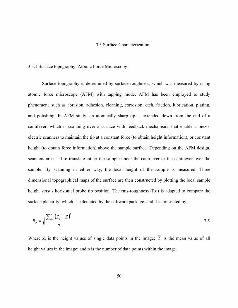
3.3 Surface Characterization
3.3.1 Surface topography: Atomic Force Microscopy
Surface topography is determined by surface roughness, which was measured by using
atomic force microscope (AFM) with tapping mode. AFM has been employed to study
phenomena such as abrasion, adhesion, cleaning, corrosion, etch, friction, lubrication, plating,
and polishing. In AFM study, an atomically sharp tip is extended down from the end of a
cantilever, which is scanning over a surface with feedback mechanisms that enable a piezo-
electric scanners to maintain the tip at a constant force (to obtain height information), or constant
height (to obtain force information) above the sample surface. Depending on the AFM design,
scanners are used to translate either the sample under the cantilever or the cantilever over the
sample. By scanning in either way, the local height of the sample is measured. Three
dimensional topographical maps of the surface are then constructed by plotting the local sample
height versus horizontal probe tip position. The rms-roughness (Rq) is adapted to compare the
surface planarity, which is calculated by the software package, and it is presented by:
( )n
ZZR
n
i iq
∑=−
= 1
2
3.5
Where Zi is the height values of single data points in the image; Z is the mean value of all
height values in the image; and n is the number of data points within the image.
50
AFM experiments were performed on a Digital Instruments Dimension Series 3100 AFM
using Tapping ModeTM to determine the nanoscale morphology of the copper surface after CMP.
A ‘nano-roughness’, or secondary roughness, as to equation 3.5, is subsequently calculated for
these high areas to compare the surface finish for Cu CMP in different conditions.
3.3.2 Scanning Electron Microscope (SEM)
Surface morphology studies were conducted using a JSM-6400F SEM system with an
Everhart-Thornley (E-T) detector. SEM images were taken at a magnification of 15,000 and an
accelerating voltage of 15 kV on 1cm×1cm Cu samples. The samples were immersed in various
solutions for 60 minutes and then wet cleaned and dried in air before imaging. The immersion
time prior to SEM imaging was much longer than the time used in the CMP process.
3.3.3 X-ray Photoelectron Spectroscopy (XPS)
Surface chemistry studies were carried out using XPS technique. XPS, also called
electron spectroscopy for chemical analysis (ESCA), has been widely used for surface chemistry
analysis. In XPS studies, x-rays produced by electron bombardment of Mg or Al targets are used
to excite photoelectrons from the sample surface, and the emitted electron signal is plotted as a
51

spectrum of binding energies. Different chemical states resulting from compound formations are
reflected in the photoelectron peak positions and shapes. Spectral information is collected from a
depth of 2 to 20 atomic layers, depending on the material studied (Schroeder, 1998).
In this study, the surface modification of copper specimens in solutions containing
various chemical constituents (e.g. H2O2, glycine, and ATA) at different pH values was
characterized using a 5400 PHI ESCA XPS system. At first, the XPS samples were immersed in
chemical solutions for 10 minutes and cleaned and dried in an inert atmosphere. Then the
cleaned samples were transferred to the vacuum chamber quickly with care to avoid further
surface modification. The base pressure during analysis was 10-9 Torr with Mg-Kα X-radiation
(1253.6 eV) at a power of 350 watts. Both the survey and the high-resolution narrow spectra
were recorded with electron pass energy of 44.75 eV and 35.75 eV, respectively, to achieve the
maximum spectral resolution. The charging shift produced by the samples was carefully
removed by using a B.E. scale referred to C (1s) B.E. of the hydrocarbon part of the adventitious
carbon line at 284.6 eV. Non-linear least square curve fitting was performed using a
Gaussian/Lorentzian peak shape after background removal.
52

CHAPTER FOUR : RESULTS AND DISCUSSION
4.1 Removal rate, etch rate, and surface finish
Removal rate (polishing rate) and surface planarity are two major CMP output
parameters. Static etch rate is a parameter that may indicate the resulting surface planarity status.
For a preliminary investigation, several complexing agent-inhibitor combinations were selected
as chemical additives for removal rate studies from a group of three complexing agents (glycine,
EDA, and citrate also called citric acid) and three inhibitors (ATA, BTA, thiourea). Etch rate
measurements were conducted in chemical solutions with the same chemical ingredients as in the
slurry except for the abrasives. Two slurry chemistry combinations (glycine+ATA and
EDA+ATA) seem to deliver good performance at basic pH values in terms of high removal rates
and low etch rates. Further, surface finish quality was determined by AFM study after CMP
processing with four complexant-inhibitor combination candidates.
4.1.1 Removal rate vs. etch rate
Figure 4.1 shows removal rate behavior of copper in various combinations of complexing
agents and inhibitors. These combinations are listed in Table 4.1. It should be noted that each
and every removal rate reported in this chapter is an average of three data points obtained from
53

four polish runs. Glycine and citrate as complexing agents have been investigated by other
researchers, such as Szocs et al. (1999). The electrochemical effect of EDA as complexing agent
on copper dissolution has been reported by Aksu et al. (2002). BTA as inhibitor has been widely
used in copper CMP by academic researchers (Luo et al., 1997). ATA is also an effective
inhibitor for copper corrosion yet its inhibitive performance is lacking in the field of Cu CMP.
BTA and ATA are both triazole derivative compounds. Thiourea as inhibitor for Cu etching has
been investigated for electrochemical deposition.
Figure 4.1 Removal rate of Cu in H2O2 based slurries with different combinations of
complexing agents and inhibitors at various pH values.
54
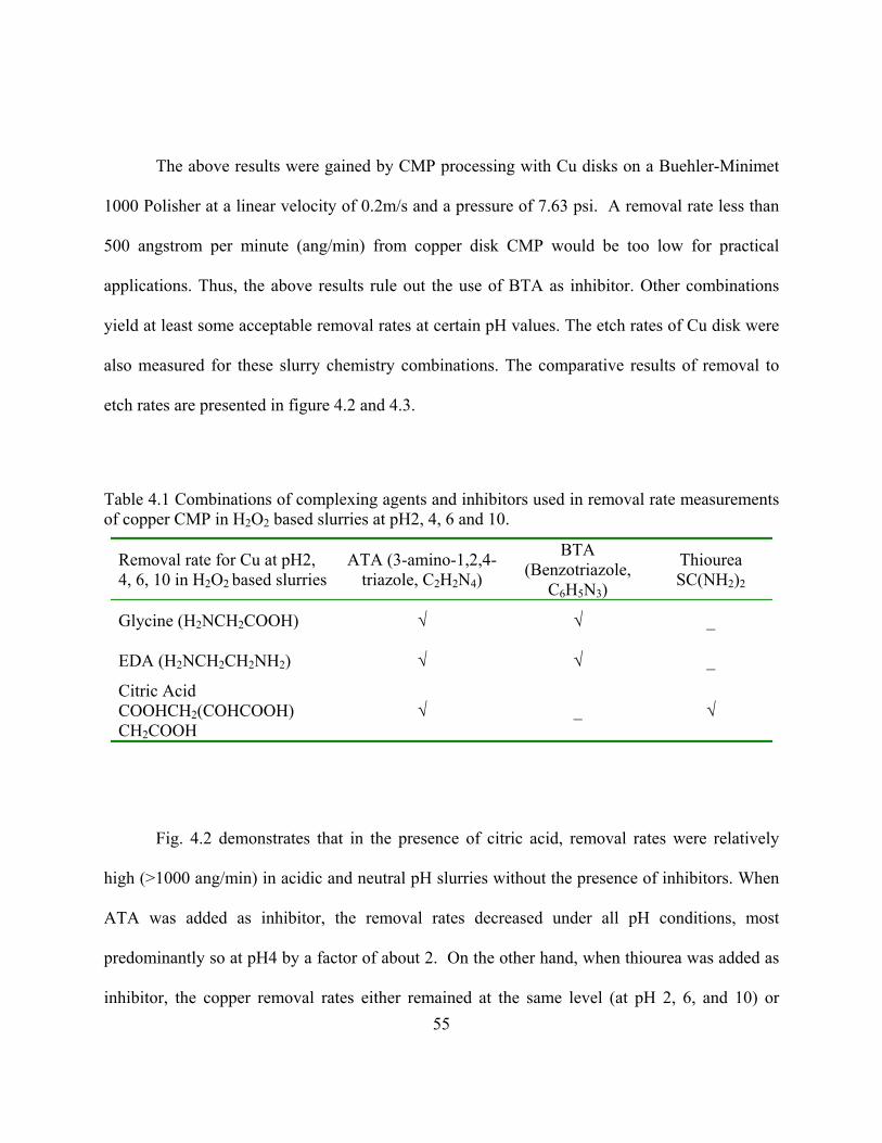
The above results were gained by CMP processing with Cu disks on a Buehler-Minimet
1000 Polisher at a linear velocity of 0.2m/s and a pressure of 7.63 psi. A removal rate less than
500 angstrom per minute (ang/min) from copper disk CMP would be too low for practical
applications. Thus, the above results rule out the use of BTA as inhibitor. Other combinations
yield at least some acceptable removal rates at certain pH values. The etch rates of Cu disk were
also measured for these slurry chemistry combinations. The comparative results of removal to
etch rates are presented in figure 4.2 and 4.3.
Table 4.1 Combinations of complexing agents and inhibitors used in removal rate measurements of copper CMP in H2O2 based slurries at pH2, 4, 6 and 10.
Removal rate for Cu at pH2, 4, 6, 10 in H2O2 based slurries
ATA (3-amino-1,2,4-triazole, C2H2N4)
BTA (Benzotriazole,
C6H5N3)
Thiourea SC(NH2)2
Glycine (H2NCH2COOH) √ √ _
EDA (H2NCH2CH2NH2) √ √ _
Citric Acid COOHCH2(COHCOOH) CH2COOH
√ _ √
Fig. 4.2 demonstrates that in the presence of citric acid, removal rates were relatively
high (>1000 ang/min) in acidic and neutral pH slurries without the presence of inhibitors. When
ATA was added as inhibitor, the removal rates decreased under all pH conditions, most
predominantly so at pH4 by a factor of about 2. On the other hand, when thiourea was added as
inhibitor, the copper removal rates either remained at the same level (at pH 2, 6, and 10) or 55

increased (at pH4), as compared to the case with citric acid alone. The same trend was observed
for etch rates with the addition of thiourea. One obvious explanation is that thiourea was not
acting as an inhibitor when combined with citrate in dynamic CMP or static etching processes,
and some other removal mechanisms were operative here.
0
500
1000
1500
2000
2500
3000
2 4 6 10pH
Rem
oval
rate
/etc
h ra
te (A
ng/m
in)
Removal rate-citric acidRemoval rate-citric acid+ATARemoval rate-citric acid+thioureaEtch rate-citric acidEtch rate-citric acid+ATA Etch rate-citric acid+thiourea
Figure 4.2. Removal rates vs. etch rates of copper disk in H2O2 based slurries/solutions with citric acid as complexant and ATA or thiourea as inhibitor at pH 2, 4, 6, and 10.
When EDA was added as complexing agent, as shown in fig. 4.3, at pH 10 high copper
removal rate is produced. However, further addition of ATA as inhibitor makes pH4 the best
condition for good inhibition performance, with an acceptable removal rate 929 ang/min. Thus
the more suitable slurry chemistry for copper removal is at pH 10 although the etch rate is quite
high at this pH. Fig. 4.3 also presents removal and etch rate results where glycine was added as
56

complexing agent. It shows clearly that pH 10 is the only good condition, under which the
combination of glycine and ATA gives an acceptable removal rate (>600 ang/min) with a
surprisingly low etch rate. This combination is expected to deliver good planarity.
0
200
400
600
800
1000
1200
1400
1600
Rem
oval
rate
/etc
h ra
te (a
ng/m
in)
pH2 pH4 pH6 pH10
Removal Rate-EDA+ATA
Etch Rate-EDA+ATARemoval Rate-glycine+ATA
Etch Rate-glycine+ATA
Figure 4.3 Removal rates vs. etch rates of copper disk with glycine/EDA as complexant, with or without ATA as inhibitor in H2O2 based slurries/solutions at pH 2, 4, 6, and 10.
To find the best pH condition for each and every combination of complexing agents and
inhibitors, as the first step, the ratio of removal rate to etching rate is used as a parameter to
measure slurry effectiveness in CMP performance. These ratios at various pH values are shown
in fig. 4.4. It is believed that higher the rate ratio, better the surface quality. Fig. 4.4 shows that
several combinations such as glycine+ATA at pH 4 and 10, EDA+ATA at pH4, and
citrate+ATA at pH10 may deliver better planarity as compared to other combinations and
conditions. 57

Figure 4.4 Rate ratio (Removal rate to etch rate) for copper with different combinations of complexing agents and inhibitors in H2O2 based slurries/solutions at pH 2, 4, 6, 10.
It should be noted that this study is for bulk copper CMP (not in combination with barrier
layers, etc.), a high removal rate is very important while a good surface finish is also required. In
this study, six combinations of complexing agents and inhibitors were chosen for investigation at
four different pH values, as shown in table 4.2. In the screening process, combinations with the
highest removal rates less than 500 ang/min were discarded. The remaining combinations were
further investigated each for one pH condition, where the highest removal rate was produced.
58

Table 4.2 Removal rates (Ang/min) for 6 combinations of complexants and inhibitors in H2O2 based slurries at pH value of 2, 4, 6 and 10.
Complexant+Inhibitor pH2 pH4 pH6 pH10
glycine+ATA 536 488 0 714 EDA+ATA 214 667 810 1476
citric acid+ATA 1131 929 1226 357
glycine+BTA 0 0 0 179
EDA+BTA 357 167 429 464
citric acid+Thiourea 1929 2440 1476 393
The dark figures in table 4.2 are highest removal rates (>500 ang/min) for the
combinations of complexants and inhibitors at certain pH values. Those are the combinations and
their pH conditions that were chosen for further investigations. It should be noted that for the
combination of citrate+ATA, a pH condition (pH4) with lower removal rate was chosen,
considering a relatively low etch rate and a fairly high removal rate at this pH.
4.1.2 Copper disk vs. thin film
A comparative performance study between copper disk and copper thin film was carried
out for the slurry chemistries selected from table 4.2. Removal rate data for copper disks and thin
films in these four slurry chemistries are presented in figure 4.5. The data suggest that the
59

removal rates of copper thin films are about 3 to 5 times higher than those of copper disks.
Although the actual removal rates for Cu thin films may differ from that of Cu disks, the trend
remains the same.
714
1476929
2440
9420
4960
35802900
0
2000
4000
6000
8000
10000
gly+ATA EDA+ATA citrate+ATA citrate+Thiourea
Removal rate(ang/min)-copper disk Removal rate(ang/min)-copper thin film
Figure 4.5 Removal rate data of copper disk and thin film for four different slurry chemistries in H2O2 based slurries.
It should be noted that CMP of copper disk was carried out on a table top polisher with a
fixed platen, while CMP of copper thin film was carried out on a polisher with a rotating table
that closely resembles an industrial grade polisher. The mechanical input parameters, such as
table speed, substrate-rotating speed, as well as pressure for those two cases are completely
different. The input parameters for CMP of copper disk were set in order to obtain comparable
data among the group members. While for thin film CMP, the input parameters were selected
60

according to concurrent industrial practices. For example, the pressure during CMP of thin films
was 4 psi as compared to 7.14 psi for that of Cu disks. It should be noted that for all the chemical
combinations, the removal rates for Cu films range from 2900 to 9420 angstrom per minute,
which are desirable for ideal industrial CMP slurries (removal rates of 2000-8000 ang/min are
expected in industrial applications).
Surface roughness of polished surfaces was measured using AFM in the tapping mode.
The surface roughness data are presented in Fig. 4.6 with root mean square (rms) values in
nanometers. Fig. 4.6 compares the roughness data for polished surfaces of Cu disks with those for
thin films. The surface roughness for copper thin film is higher in all slurries than that for copper
disks after CMP. For copper disks, all slurry chemistries yielded comparable surface finish
quality.
1.6 1.99 2.3 2.52.451 2.25
10
5.867
-113579
111315
gly+ATA EDA+ATA citrate+ATA citrate+Thiourea
Roughness(nm)-copper disk Roughness(nm)-copper thin film
Figure 4.6 Surface roughness data of copper disks and thin films after CMP in H2O2 based slurries with different slurry chemistry.
61
It is clear from Fig. 4.6, that two combinations, glycine+ATA and EDA+ATA exhibit
much better surface finish (roughness) performances than citrate+ATA or citrate+thiourea. It is
worth noting that generally copper thin film is more fragile to corrosion and contamination than
copper disks, and thus thin film is more challenging in post-CMP cleaning. Usually de-ionized
water plus acetone is enough for disk cleaning after CMP. It clearly is not as good for copper
thin film cleaning. It is suggested that contaminated surfaces due to non-effective post-CMP
cleaning may affect the surface roughness measurements for copper thin films. The small
roughness difference between copper disks and thin films for the slurries with glycine+ATA and
EDA+ATA might indicate that under those two slurry chemistry conditions, surface
contamination is much less than that for the other two slurries. It should be noted that for
glycine+ATA and EDA+ATA, the pH value was maintained at pH 10 while for the other two
cases pH 4 was maintained. It is known that pH affects particle stability and particle-metal
interaction behavior. The roughness gap between copper disks and thin films may largely be
impacted by the effect of different pH values rather than slurry chemical constituents.
4.1.3 Glycine vs. EDA as complexing agent
With microelectronic devices continually scaling down to smaller dimensions, there is
less tolerance in surface planarity. The current focus of CMP is on planarity as well as Cu/low-k
compatibility. For this consideration, glycine and EDA were chosen as complexing agent owing
62

to their good performance on surface planarity during copper CMP (indicated by a higher ratio of
removal rate to etch rate), and superior surface finish, especially for copper thin films.
To obtain a complete picture of the copper removal during CMP, copper removal rates
without complexing agents, with complexing agents, and with complexing agents plus inhibitor
(ATA) were measured for four different slurry chemistries. The results for both glycine and EDA
as complexant are demonstrated in Fig. 4.7. It should be noted that all the data hereinafter were
gathered using copper disks. It has been independently reported by other work that copper disks
show the same trend in CMP performance as copper thin films (Li et. al., 2003). Therefore, the
information collected from CMP of copper disks should be valid for thin films.
Fig. 4.7 (a) shows the copper CMP removal rates as a function of pH in H2O2 based
slurries, without glycine, with glycine, and with glycine plus ATA. In the absence of glycine,
the removal rate decreases with the increase of pH, and reaches the minimum at pH 6. With the
pH moving to the alkaline region, the removal rate increases. In the presence of 0.01 M glycine,
the removal rate decreases from the acidic to neutral pH region, then increases significantly
after pH 6, and reaches the highest value at pH 10. With further addition of ATA as inhibitor,
the copper removal rate is suppressed at all pH values, while the trend remains the same as in
the case with glycine, without inhibitors.
From applications point of view, it is clearly shown that only at pH 10 glycine+ATA
delivers an acceptable copper removal. In the case of EDA+ATA, all pH conditions are good for
copper removal except at pH 2. To understand the copper removal mechanisms for the slurries
63

with glycine/EDA, electrochemical techniques were employed and the results are discussed in
the next section.
(a)
0200400600
800100012001400
0 2 4 6 8 10 12pH
Rem
oval
rate
(Ang
/min
No additives glycine glycine+ATA
(b)
0
500
1000
1500
2000
0 2 4 6 8 10pH
Rem
oval
rate
(Ang
/min
12
)
No additives EDA EDA+ATA
Figure 4.7 Removal rate data for copper disk CMP in H2O2 based slurries at pH values of 2, 4, 6 and 10. (a). Removal rates in slurries without additives, with glycine, and with glycine+ATA. (b). Removal rates in slurries without additives, with EDA, and with EDA+ATA.
64

4.2 Electrochemical investigations
Electrochemical studies are mainly applied to understand the effect of chemical
component in copper removal mechanisms. Ex-situ electrochemical measurements such as
potentiodynamic polarization and EIS scan were specially employed. The results were analyzed
and the data used to correlate with copper etch rate results. Thus, copper etch rate data as well as
electrochemical testing results are presented and compared for both slurry chemistries containing
glycine or EDA. Firstly, an investigation of the Cu-H2O2-glycine system was conducted to
understand the role of glycine as complexing agent in copper CMP. Then, two complete systems
including both complexing agent and inhibitor are studied with one system Cu-H2O2-glycine-
ATA under pH 10 condition and another Cu-H2O2-EDA-ATA under all pH conditions.
4.2.1 Cu-H2O2-glycine system
Potentiodynamic polarization can be used to measure the corrosion current density (Icorr)
and corrosion potential (Ecorr). Icorr and Ecorr can be used as parameters to determine the surface
modification behavior of copper in different slurry chemical solutions. Fig. 4.8 presents the
polarization plots for copper surface immersed in H2O2 based solutions containing glycine at
various pH values.
65
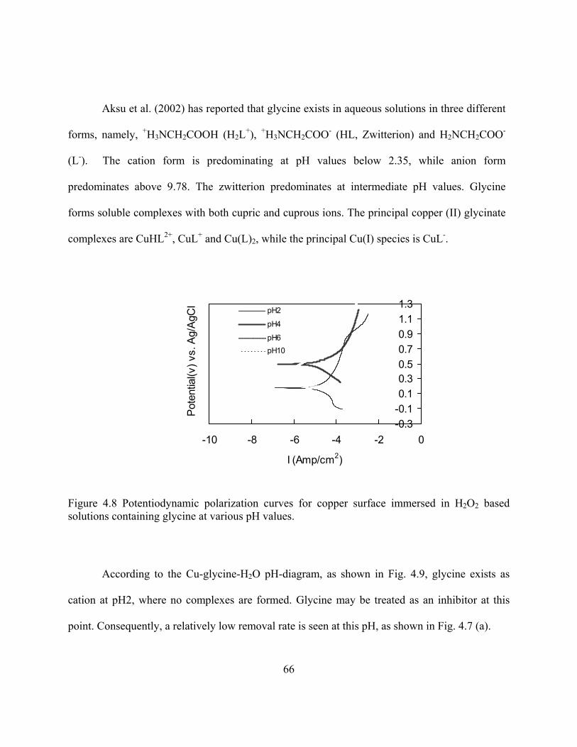
Aksu et al. (2002) has reported that glycine exists in aqueous solutions in three different
forms, namely, +H3NCH2COOH (H2L+), +H3NCH2COO- (HL, Zwitterion) and H2NCH2COO-
(L-). The cation form is predominating at pH values below 2.35, while anion form
predominates above 9.78. The zwitterion predominates at intermediate pH values. Glycine
forms soluble complexes with both cupric and cuprous ions. The principal copper (II) glycinate
complexes are CuHL2+, CuL+ and Cu(L)2, while the principal Cu(I) species is CuL-.
-0.3-0.10.10.30.50.70.91.11.3
-10 -8 -6 -4 -2
I (Amp/cm2)
Pote
ntia
l(v) v
s. A
g/Ag
Cl
0
pH2
pH4
pH6pH10
Figure 4.8 Potentiodynamic polarization curves for copper surface immersed in H2O2 based solutions containing glycine at various pH values.
According to the Cu-glycine-H2O pH-diagram, as shown in Fig. 4.9, glycine exists as
cation at pH2, where no complexes are formed. Glycine may be treated as an inhibitor at this
point. Consequently, a relatively low removal rate is seen at this pH, as shown in Fig. 4.7 (a).
66

Figure 4.9 Potential-pH diagram for Cu-glycine system.
0
100
200
300
400
500
0 2 4 6 8 10 12pH
Icor
r/uA.
cm-2
Without glycine
w ith 0.01M glycine
Figure 4.10 Variation of Icorr values of copper surface in H2O2 based solutions with and without 0.01 M glycine at various pH values.
67
Fig. 4.10 shows a plot of corrosion current density as a function of pH in H2O2 based
solutions with and without 0.01 M glycine (Du et al., 2003). In the absence of glycine, Icorr
decreases as pH increases in the acidic region, and it reaches the minimum at pH 6. Then Icorr
increases slowly in the alkaline region. The decrease of Icorr in the acidic region may suggest a
thicker protective passive film formation with increasing pH. On the other hand, in the presence
of glycine, Icorr remains at the same low level in the acidic region while increasing significantly in
the alkaline region. The low value of Icorr at pH 2 can be explained by the inhibitive effect of
glycine at this point. The increase of Icorr from pH 6 to pH 10 may be due to the catalytic behavior
of glycine with the formation of highly soluble copper complexes. A more detailed investigation
of Cu-H2O2-glycine-ATA system at pH 10 is presented in the next section.
4.2.2 Cu-H2O2-glycine-ATA system
Due to the expected good performances in removal rate and planarity, the Cu-H2O2-
glycine-ATA system at pH 10 was further investigated. First of all, the removal rate vs. etch rate
data for copper in H2O2 based slurries/solutions without glycine, with glycine, and with glycine
plus ATA are presented in Fig. 4.11. The very low etch rate of copper in solutions containing
glycine+ATA is desirable for a good global planarity performance.
68

25.3 2.98287
7.44309.52 393
1476
714
0300600900
120015001800
5vol
%h2
o2
5vol
%h2
o2+0
.1w
t%AT
A
5vol
%H
2O2+
0.1w
t%AT
A+0.
01M
eda
5vol
%H
2O2+
0.1w
t%AT
A+0.
01M
glyc
ine
etch rateremoval rate
Figure 4.11 Removal rate (Ang/min) vs. etch rate (Ang/min) data for copper in H2O2 based slurries/solutions without glycine, with glycine, and with glycine plus ATA at pH 10.
To confirm the data from static etch, potantiodynamic polarization was used for copper
surface at the three above-mentioned conditions and the results are shown in Fig. 4.12. Little
difference is shown in the anodic region among all the solutions. Very clear difference among
these conditions is present in the cathodic polarization region. It is also noted that corrosion
potentials (Ecorr) seem identical in all the conditions, indicating that glycine or ATA does not
affect the corrosion potential of copper as H2O2.
The corrosion potential (Ecorr) and corrosion current density (Icorr) data derived from Fig.
4.12 were used to analyze the electrochemical behavior of copper, as listed in table 4.3. The Icorr
in the case with glycine+ATA is extremely low, corresponding to the extremely low etch rate.
Meanwhile, Icorr in the case without glycine is lower than that of the case with glycine,
corresponding to the lower etch rate in the former case.
69

-0.3
-0.1
0.1
0.3
0.5
0.7
0.9
1.1
1.3
-10 -8 -6 -4 -2I (Amp/cm2)
0
Pote
ntia
l(v) v
s. A
g/Ag
Cl
5vol%h2o2
5vol%h2o2+0.01Mglycine
5vol%h2o2+0.01Mglycine+0.1wt%ATA
Figure 4.12 Potentiodynamic polarization plot for copper surface immersed in H2O2 based solutions without glycine, with glycine, and with glycine plus ATA at pH 10.
Table 4.3 Corrosion potential and corrosion current density data derived from Fig. 4.12.
5vol%H2O2 5vol%H2O2
+0.01Mglycine
5vol%H2O2+0.01M Glycine
+0.1wt%ATA
Ecorr(V) 0.1974 0.1974 0.199
Icorr(mA/cm2) 0.903 1.299 0.03
It should be noted that in the case without glycine, etch rate is 4 orders of magnitude
lower than that in the case with glycine, while the Icorr difference between the two cases is not so
huge. It might be due to the fact that the etch rate measurements of copper were taken after 60 70

minute’s immersion, while the polarization dynamic curve is usually obtained after less than 20
minute’s immersion. It is known that surface modification from electrochemical behavior is
controlled by chemical reaction kinetics. The surface modification of the Cu-H2O2–glycine
system at pH 10 is controlled by several chemical reactions including copper oxidation by H2O2
as well as Cu-glycine complexation, as listed below:
OHOCuOHCu 22222 +=+ 4.1
OHCuOOHOCu 2222 2 +=+ 4.2
( ) OHLCuHLCuO 222 +=+ 4.3
OHCuOOHCu 2)(*2 +=+ 4.4
It is shown that the complexing reaction of glycine consumes copper oxides, as shown in
equation 4.3, which drives the copper oxidation reaction to the right side as shown in equations
4.1 and 4.2. It has also been reported that the Cu-glycine complexes catalyze the decomposition
of H2O2 by producing copious amount of *OH radicals in the bulk slurry, which again enhance
the copper oxidation process according to equation 4.4 (Hariharputhiran et al., 2000). It is
suggested that glycine act as a catalyst for the accelerating process of copper oxidation and
dissolution. ATA shows highly effective inhibitive behavior for copper surface passivation.
71

-360
-260
-160
-600 60 120 180 240 300 360
Real Impedance ( ohm.cm2 )Imag
inar
y Im
peda
nce
( ohm
.cm
2 )
5vol%h2o2
5vol%h2o2+0.01Mglycine
5vol%h2o2+0.01Mglycine+0.1wt%ATA
Figure 4.13 EIS Nyquist plot for copper surface immersed in H2O2 based solutions without glycine, with glycine, and with glycine plus ATA at pH 10.
It is well known and has been mentioned that polarization resistance Rp is inversely
proportional to Icorr and it is therefore also inversely proportional to the etch rate. The EIS Nyquist
plots as shown in Fig. 4.13 demonstrate the agreement with the etch rate data and the
potentiodynamic polarization results. It should be noted that the EIS measurements were carried
out under the same conditions as the potentiodynamic scans. So the comparison between the EIS
results vs. etch rates and the polarization results vs. etch rates should give identical results.
72

4.2.2 Cu-H2O2-EDA-ATA system
Similar electrochemical studies were conducted for the Cu-H2O2-EDA-ATA system,
except that for this system, pH values ranging from 2, 4, 6, and 10 were considered instead of just
pH 10, and pH is the only varying parameter for this investigation.
In order to correlate the electrochemical data with the static etch data, firstly, the removal
rate vs. etch rate data for the Cu-H2O2-EDA-ATA system is presented in Fig. 4.14. The removal
rate at pH 10 is very promising. Although it need to be noted that it is at pH 4 that a much better
global planarity could be expected because of a very low etch rate at this pH. A particular
investigation for this case may be necessary in future studies. The data for the Cu-H2O2-EDA
system without the addition of ATA are also shown in this figure.
Fig. 4.15 shows the potentiodynamic curves for the Cu-H2O2-EDA-ATA system at
different pH values. The derived data for Ecorr and Icorr are plotted in Fig. 4.16. The Icorr at
different pH values correlates well with the etch rate data shown in Fig. 4.14. It is seen that Ecorr
varies with different pH values, indicating that different copper oxidation behavior affected by
H2O2 is a function of pH.
73

0
500
1000
1500
2000
2500
pH2 pH4 pH6 pH10
Removal Rate-EDA
Removal Rate-EDA+ATA
Etch Rate-EDA
Etch Rate-EDA+ATA
Figure 4.14 Removal rate vs. etch rate data for the Cu-H2O2-EDA-ATA system at various pHs.
-0.3-0.10.10.30.50.70.91.11.3
-8 -6 -4 -2 0
I (Amp/cm2)
Pote
ntia
l(v) v
s. A
g/Ag
Cl pH2
pH4 pH6 pH10
Figure 4.15 Potentiodynamic curves for copper surface immersed in H2O2 based solutions with EDA plus ATA at pH 2, 4, 6, and 10.
74

00.10.20.30.40.5
0 2 4 6 8 10 12pH
Ecor
r(V)
05001000150020002500
Icor
r(mA/
cm2)
EcorrIcorr
Figure 4.16 Corrosion potential and corrosion current density data derived from Fig. 4.15.
Further correlations are made by using EIS scans, as shown in Fig. 4.17. It should be
particularly noted that the Rp value is extremely high at pH 4, indicating a very low etch rate at
this condition. The electrochemical data of the Cu-H2O2-EDA-ATA system correlate well with
the etch rate data.
A simple equivalent circuit as shown in Figure 4.18 was used to fit the EIS spectra of
copper. In the circuit, Rs represents the solution resistance, R1 and C1 represent the resistance and
capacitance of the double layer at the solid-liquid interface, respectively, and R2 and C2 refer to
the resistance and capacitance of the film formed on copper surface, respectively. The equivalent
circuit fitted well with the EIS spectra, with a fitting error less than 5%. Rp value was calculated
by adding Rs with R1 and R2. The extremely high Rp value of 2274.09 ohm at pH4 agrees well
with the extremely low etch rates as shown in Fig. 4.14. Another extreme is the lowest Rp value
75

of 338.18 ohm at pH 10, corresponding to both the highest etch rate and the highest removal rate
at this pH as shown in Fig. 4.14.
-4000
-3500
-3000
-2500
-2000
-1500
-1000
-500
00 500 1000 1500 2000 2500 3000 3500 4000
Real Impedance ( ohm.cm2 )
Imag
inar
y Im
peda
nce
( oh
m.c
m2 ) pH2 pH4
pH6 pH10
Figure 4.17 EIS Nyquist plot for copper surface immersed in H2O2 based solutions with EDA plus ATA at pH 2, 4, 6, and 10.
R1 R2 Rs
C1 C2
Figure 4.18 Equivalent circuit for fitting the EIS Nyquist plot shown in Fig 4.17.
76

Table 4.4 Rp values for the Cu-H2O2-EDA-ATA system at different pH values.
Rp value PH value
849.17 ohm pH 2
2274.09 ohm pH 4
709.2 ohm pH 6
338.18 ohm pH 10
4.3 Surface analysis
4.3.1 XPS analysis
XPS has been widely used to study the surface chemistry of copper after exposure to
various slurry chemistries (Nishi et al., 2003). In this study, XPS was employed to understand
the chemical interactions of the Cu-H2O2-glycine-ATA system at the copper-slurry chemistry
interface in static conditions. Surface chemistry analysis of copper was performed in slurry
chemical solutions at conditions without glycine, with glycine, and with glycine plus ATA.
Fig. 4.19 presents the Cu 2p3/2 XPS spectra of copper after 10-minute immersion in
H2O2 based solutions at pH values of interest. The characteristic binding energy (BE) of Cu2O of
932.2 eV is observed in all the cases. The relatively high photoelectron signal intensity for the
cases at pH 2, pH 4, and pH 10 is obtained compared to the case of pH 6. Since the binding 77

energy of Cu2O is very close to that of copper metal (933.5 eV), it is suggested that these signals
are responding not only from cuprous oxide on the surface, but from the substrate copper metal
as well. The deconvolution of the XPS spectra reveals two additional peaks presented at 933.5
eV and 934.5 eV for cases of pH 2 and pH 6. It is known that the binding energies of copper in
CuO and Cu(OH)2 are 933.4±0.2 eV and 934.5±0.2 eV, respectively. The signals of CuO can be
identified clearly for the pH 6 case. It is characteristic of CuO to have the shakeup satellite
feature at a binding energy of 10 eV higher than that of the Cu 2p3/2 peaks (933.5 eV).
928933938943948
Binding Ene rgy/e V
Cou
nts
/arb
.uni
ts (a)
(b)
(c)
(d)
Cu/Cu2O
CuO Cu(OH)2 CuO satellite
Figure 4.19 Cu (2p3/2) XPS of copper oxide films formed after 10 minute immersion in 5% H2O2 solutions at (a) pH 2, (b) pH 4, (c) pH 6, and (d) pH 10.
78

These discussions can be further confirmed using CuLMM Auger lines, as shown in Fig.
4.20. In the pH 2 case, a high Cu2O CuLMM peak is ahown at the binding energy of 337.5 eV. A
small shoulder is shown at BE 335.0 eV, which is generated by the substrate copper metal. And a
big shoulder is shown at BE 335.8 eV, which is generated by CuO. In the pH 4 case, a strong Cu
peak and a smaller Cu2O Auger peak are presented, implying a thinner oxide film formation at
this point. In the pH 6 case, the spectrum shows a very small Cu2O peak, which is overlapped
also by weak copper metal Auger lines at BE 335.0 eV and CuO Auger lines at BE 335.8 eV.
The concentration ratio of cuprous oxide and cupric oxide may affect the copper removal
behavior since the mechanical strength is different for the two oxides. In the pH10 case, the
spectrum shows a strongest Cu2O signal, which is overlapped with a weak Cu signal from the
substrate. The relatively strong signal of Cu2O in the pH10 case may indicate a thicker film
formation.
79

330335340345350
Bind ing Ene rgy/e V
Cou
nts
/arb
. un
its
(a) (b)
(c)
(d)
Cu Cu2O
Figure 4.20 XPS Cu LMM Auger lines of copper oxide films formed after 10 minute immersion in 5% H2O2 solutions at (a) pH 2, (b) pH 4, (c) pH 6, and (d) pH 10.
928933938943948
Binding Ene rgy/e V
Cou
nts/
arb.
uni
ts
(a) (b)
(c)
(d)
Cu/Cu2O
CuO CuO satellite
Figure 4.21 Cu (2p3/2) XPS of copper oxide films formed after 10 minute immersion in solutions with 5% H2O2 and 0.01 M glycine at (a) pH 2, (b) pH 4, (c) pH 6, and (d) pH 10.
80

Fig. 4.21 shows the Cu 2p3/2 XPS spectra of copper surface after 10-minute immersion
in the H2O2 based solutions containing glycine at the pH values of interest. The XPS core level
Cu(2p) peak of the pH 2 case suggests the presence of cupric oxide. A cupric oxide satellite peak
is also observed on the copper surface in the pH 2 case. In the pH 4 case, an XPS core level
Cu(2p) peak appears at 932.5eV, corresponding to metallic copper or cuprous oxide. The
deconvolution of this peak reveals the presence of cupric oxide. The decreased removal rate of
copper in slurries containing glycine in the acidic region may be due to the enhanced formation
of cupric oxide. On the other hand, in the case of pH 6, a main Cu(2p) peak is shown,
corresponding to the metallic copper with little evidence of copper oxides. This observation
indicates a poor copper oxidation behavior. In the pH 10 case, a big cuprous peak suggests that
in the presence of glycine, the Cu-glycine complex formation accelerates the copper oxide
formation, most evidently the cuprous oxide formation.
The XPS Cu(2p) spectra of copper surface after 10 minute immersion in H2O2 based
solutions containing glycine plus ATA are shown in Fig. 4.22. Little evidence of cuprious oxide
formation is shown in the spectra. It is suggested that with the addition of ATA as inhibitor, the
cuprious oxide formation is highly suppressed. It is worth noting that in the cases of pH 2, pH 4,
and pH 10, rather strong Cu/Cu2O peaks are shown as compared with the case of pH 6. This
observation suggests that the oxide formation is necessary for copper removal.
To further confirm the effects of ATA adsorption and the Cu-glycine complexation on
the copper surface, the XPS spectra of N(1s) of copper surface after 10 minute immersion in
H2O2 based solutions with glycine and with glycine plus ATA are presented in Figs. 4.23. An
81

XPS N (1s) peak appeared at 397.1 eV in the case of glycine, which indicates the presence of
Cu-glycine complex on the surface. The relatively low intensity of this N(1s) peak suggests that
this Cu-glycine complex is highly soluble. XPS N(1s) peak appears at 400 eV in the case of
glycine plus ATA. Deconvolution of this N (1s) peak reveals two separate peaks: One peak at
398.9 eV corresponds to the amino group on the ATA molecule; the other peak at 400.1 eV
corresponds to the N on the triazole ring on the ATA molecules. These observations indicate that
the ATA molecules are preferentially adsorbed onto the copper surface and inhibit the oxide
formation. Similar results are observed for other pH conditions.
928933938943948
Binding Ene rgy/e V
Co
unts
/arb
. uni
t
(a)
(b)
(c)
(d)
Cu(2p3/2)
Figure 4.22 Cu (2p3/2) XPS of copper oxide films formed in solutions with 5% H2O2, 0.01M glycine, and 0.1wt% ATA after 10-minute immersion at (a) pH 2, (b) pH 6, (c) pH 4, and (d) pH 10.
82

390 395 400 405
Binding Energy (eV)
Inte
nsity
(a)
395 397 399 401 403 405
Binding Energy (eV)
Inte
nsity
1
2
(b)
Figure 4.23 XPS N(1s) spectra of Cu surface after 10 minute immersion in H2O2 based solutions at pH10 containing (a) 0.01M glycine and (b) 0.01M glycine and 0.1wt% ATA.
83

4.3.2 SEM analysis
Fig. 4.24 shows the SEM images of copper surface after 60 minute’s immersion in H2O2
based solutions at different pH values. The image of copper surface in the pH 2 solution shown
in Fig 4.24 (a) indicates that a strong etch reaction occurs and the surface is covered with a
discontinuous layer of amorphous corrosion product, which are Cu2O and CuO according to the
XPS analysis. In this condition, active dissolution of copper predominates in the CMP process,
resulting in a higher CMP removal rate. Fig. 4.24 (b) shows the copper surface morphology in
pH 4 solutions. The polishing scratches on the substrate surface can still be seen even after 60-
minute immersion, indicating a low film formation rate. This observation is also in agreement
with the XPS results. Fig. 4.24 (c) shows the surface morphology in the pH6 solution. The whole
surface seems to be covered with monoclinic CuO and Cu2O crystals. This film is porous yet
compact and protective. Since the oxide film of CuO is much harder than pure copper (Liang et
al., 2001), a relatively lower CMP removal rate is observed in this case. Fig. 4.24 (d) shows the
copper surface morphology in pH 10 solutions. A much thicker film seems to be formed on the
substrate surface, yet it seems to be loosely attached to the substrate surface, since many cracks
of the oxide film are also shown. This kind of film may be easier to be removed during CMP.
84

2µ
(a)
2µ
(b)
85

2µ
(c)
2µ
(d)
Figure 4.24 SEM images of copper surface after 60-minute immersion in H2O2 based solutions at (a) pH 2, (b) pH 4, (c) pH 6, and (d) pH 10.
86

Fig. 4.25 presents the SEM images for copper surface after 60-minute immersion in H2O2
based solutions at pH 10 in cases with 0.01M glycine and with 0.01 M glycine + 0.1wt% ATA.
With the addition of glycine, the surface morphology indicates that a strong etching reaction is
taking place and many etching pits are observed in large and small scales. As a result, active
dissolution of copper predominates in the CMP process in this condition. Therefore, a higher
CMP removal rate is obtained. With the further addition of ATA as inhibitor, the surface seems
smooth. The polishing lines on the substrate surface can be identified even after 60-minute
immersion, indicating the film formation rate or the Cu dissolution rate is rather low. This is in
agreement with the XPS results, which claims that the strong adsorption of ATA molecules on
the copper surface highly inhibits the oxide formation and/or the copper dissolution.
2µ
(a)
87

2µ
(b)
Figure 4.25 SEM images of copper surface after 60-minute immersion in H2O2 based solutions at pH 10 with (a) 0.01M glycine (b) 0.01M glycine and 0.1wt% ATA.
4.3.3 AFM images
Fig. 4.26 depicts AFM images of copper surface after CMP in H2O2 based slurries at pH
10 in conditions (a) without chemical additives, (b) with 0.01M glycine (c) with 0.01 M glycine
and 0.1wt% ATA, and (d) with 0.01 M EDA plus 0.1wt% ATA. AFM measurements delivered a
surface roughness of 18.5 nm for the copper surface after CMP in H2O2 based slurries at pH10
without the addition of other chemicals. With the addition of glycine, the surface roughness
dropped tremendously to 6.7nm. This may be due to the dissolution of the copper oxides by
88

forming highly soluble Cu-glycine complexes. With further addition of 0.1wt% ATA, the surface
roughness went down to 1.6nm, suggesting that with the addition of ATA as inhibitor, a very
good surface finish is obtained.
Fig 4.22 (d) presents the AFM image of copper surface after polishing in H2O2 based
slurries with EDA and ATA with a roughness of 1.99 nm. Compared to glycine, the surface
finish of copper in the EDA case is not as desirable.
(a)
89

(b)
c )
90

(d)
Figure 4.26 AFM images of copper surface after CMP in H2O2 based slurries at pH 10 in conditions (a) without chemical additives, (b) with 0.01M glycine (c) with 0.01 M glycine and 0.1wt% ATA, and (d) with 0.01 M EDA plus 0.1wt% ATA.
91

CHAPTER FIVE : SUMMARY
1. Preliminary removal rate and static etch rate studies for copper disk were carried out by
using different combinations of complexing agents (glycine, EDA, and citrate) and
inhibitors (ATA, BTA, and thiourea) in H2O2 based slurries at pH values ranging from 2 to
10. Considering that a removal rate less than 500 ang/min is not applicable due to an
expected high cost of throughput and that a low etch rate is desirable for good global
planarity, four combinations at their certain pH conditions (glycine+ATA at pH10,
EDA+ATA at pH10, citrate+ATA at pH4, and citrate+thiourea at pH4) were chosen for
further studies including CMP of thin films and surface roughness measurements.
2. For each of the four combinations, a thin film removal, 3-5 times that of copper disk
removal was observed, with thin film removal rates ranging from 2800 to 9420 ang/min,
which are desirable for industrial applications. Better surface finish was obtained in the
cases of glycine+ATA and EDA+ATA, with roughness of 2.45 nm and 2.25 nm,
respectively, for thin films, and 1.6 nm and 1.99 nm, respectively, for copper disks. Similar
surface roughness for copper disks was also obtained in the cases of citrate+ATA and
citrate+thiouea, while for copper thin films, both cases delivered roughnesses higher than 5
nm. Such huge roughness gap for copper thin films between the former two cases and the
later two may be explained in different ways. One possible explanation is that the former
two slurry chemistries, glycine+ATA and EDA+ATA, deliver modified thin film surfaces
that are compatible to post-CMP cleaning without further contaminating or corroding the
surface; while the other two slurry chemistries,citrate+ATA and citrate+thiourea, deliver
92

corroded and/or contaminated copper surface, which resulted in much higher roughness.
Another explanation is that since the former two slurries have the same pH value of 10 and
the later two have the same pH value of 4, it may be suggested that slurries of pH 10
control post-CMP surfaces better than slurries of pH 4.
3. Based on the data of removal rate, static etch rate, and surface finish, two slurry chemistry
combinations (glycine+ATA and EDA+ATA) were chosen for electrochemical studies. Ex-
situ potentialdynamic polarization and EIS technique were employed to understand the
removal and etch performance of the Cu-H2O2-glycine system at all the pH values, the Cu-
H2O2-glycine-ATA system at pH 10, and the Cu-H2O2-EDA-ATA system at all the pH
values. Basically, the corrosion current density data derived from potentiodynamic
polarization curves and corrosion resistance data derived from EIS plots are correlated well
with the static etch results for all three systems. Moreover, the electrochemical data and the
removal rate/etch rate data can be further correlated with corresponding potential-pH
diagrams and chemical reaction kinetics. From the results and discussions, it is suggested
that the complexing effects of glycine/EDA can be explained as that the Cu-glycine/Cu-
EDA complex formation, which will accelerate the copper oxidation processes by
consuming copper oxides and by catalyzing the formation of *OH at alkaline conditions.
Thus, a highly desired copper removal is observed at pH10 in both glycine and EDA cases.
4. XPS was used for surface chemistry analysis of the Cu-H2O2 system, the Cu-H2O2-glycine
system, and the Cu-H2O2-glycine-ATA system. XPS spectra offer information about the
type of oxides formed on the copper surface and the thickness of a certain oxide. For the
93

Cu-H2O2 system, it is indicated that large amounts of Cu2O and CuO are formed on the
copper surface at pH 2 from the relatively high peaks of those two oxides. At pH 4 and pH
10, a higher Cu peak indicates a less thick oxide layer. At pH 6, all the peaks are relatively
small. It is believed that a thicker oxide layer as might expected from the pH 2 case
corresponds to a higher removal rate, which is observed at pH 2, and vise versa, as shown
for the pH6 case. Compared to the Cu-H2O2 system, larger amount of Cu2O and CuO are
found in the XPS spectra for the Cu-H2O2-glycine system at all the pH values except at pH
6. This observation confirms the previous suggestion that glycine catalyze the oxide
formation by forming Cu-glycine complexes. The XPS spectra for the Cu-H2O2-glycine-
ATA system present little evidence of CuO. A still higher Cu/Cu2O peak at pH 2, PH 10,
and pH 4 may be due to the catalytic effect of glycine. The missing of CuO may be related
to the inhibitive effect of ATA. The analysis of XPS N(1s) spectra further confirms the
complexing effect of glycine and the passivation effect of ATA absorption.
5. SEM imaging presents the surface morphology of the Cu-H2O2 system at all the pH values,
the Cu- H2O2-glycine system at pH 10, and the Cu-H2O2-glycine-ATA system at pH 10.
For the Cu-H2O2 system, the SEM image shows corrosion products formed on the copper
surface, which can be correlated to the CMP removal rate data. The addition of glycine in
the hydrogen peroxide based solutions enhances the dynamic removal rate of copper at pH
10, which is due to the formation of the highly soluble copper-glycine complexes. The
additions of ATA as inhibitor can improve the surface planarity by inhibiting the
dissolution of copper through preferential adsorption on the copper surface.
94

LIST OF REFERENCES
Aksu S. and Doyle F.M., J. Electrochem. Soc. 149, p. 340, (2002)
Aksu S. and Doyle F.M., J. Electrochem. Soc. 149, p. 352, (2002)
Aksu S., Wang L., and Doyle F.M. J., Electrochem. Soc. 150, p. 718, (2003)
Aksu S. and Doyle F.M. J. Electrochem. Soc., 148 (1) p. 51, (2001)
Braun A.E., Semidond. Int. 24, p. 51, (2001)
Brown N.J., Baker P.C., and Maney R.T., Proc. SPIE 306, p. 42, (1981)
Chu J. K., Multani J. S., Mittal S. K., Orton J. T. and Jecmen R., Proc. IEEE 4th VMIC, Santa
Clara, CA, IEEE, New York, p. 61, (1987)
Cooper K., Gupta A., and Beaudoin S., J. Electrochem. Soc. 148, p. 662, (2001)
Du T., Luo Y., and Desai V., Microelectronics Eng. 71 (1), p. 90, (2004)
Du T., Tamboli D., and Desai V., Microelectronics Eng., 69 (1), p. 1, (2003)
Du T., Tamboli D., Luo Y., and Desai V., Applied Surface Science, 229 (1-4), p. 167, (2004)
Evans D., MRS Proceddings, 732E, (2002)
Fayolle M. and Romagna F., Microelectronics Eng. 37/38, p.135, (1997)
Fury M., Levert J., Mukherjee S., and Debear D., ECS Hawaii Proceedings, (1999)
Halpern J., Milant H., and Wiles D. R., J. Electrochem. Soc., 106, p. 647, (1959)
Hariharaputhian M., Zhang J., Ramarajan S., Kelher J.J., Li Y., and Babu S.V., J. Electrochem.
Soc. 147, p. 3820 (2000)
95
Hirabayashi H., Huguchi M., Kinoshita M., Kaneko H., Hayasaska N., Mase K., and Oshima J., in
Proceedings of the 1st International Chemical-Mechanical Planarization for VLSI/ULSI
Multilevel Interconnection Conference CMP-MIC, Institute for Microelectronics
Interconnection, p. 119, (1996)
Hu C.K. and Harper J.M.E., Mater. Chem. Phys., 52, p. 5 (1998)
International Technology Roadmap of Semiconductors; ITRS Home Page,
http://public.itrs.net/Files/2001ITRS/Home.htm
Johnson H. E. and Leja J., J. Electrochem. Soc., 112, p. 638, (1965)
Kaufman F.B., Thompson D.B., Broadie R.E., Jaso M.A., Guthrie W.L., Pearson D.J., and Small
M.B., J. Electrochem. Soc. 138, p. 3462, (1991)
Lai J., Saka N., and Chun J., J. Electrochem. Soc. 149, p. 41, (2002)
Lakshminarayanan S., Steigerward J.M., Price D.T., Bourgeois M., Chow T.P., Gutmamn R.J.,
and Murarka S.P., IEEE Electron. Device Lett., 15, p. 307, (1994)
Lee A.J., Moinpour M., Liou H., and Abell T., MRS proceedings, (2003)
Li Z., Rader S., Lefevre P., Ina K., and Philipossian A. ECS proceedings, (2003)
Liang H. and Xu G.H., Scripta Materialia, 46 (5), p.343, (2002)
Liang H., Martin J.M., and Lee R., J. Electronic Materials, 30, p. 391, (2001)
Lu J., Carland J.E., Petite C.M., Babu S.V., and Roy C., Mat. Res. Soc. Symp. Proc., 767, (2003)
Luo Q., Campbell D.R., and Babu S.V., Thin Solid Films, 311, p. 177, (1997)
Luo Q. and Babu S.V., J. Electrochem. Soc. 147, p. 4639, (2000) 96
Macdonald J.R., Impedance Spectroscopy, Wiley, New York, 1987
Mahajan U., Bielmann M., and Singh R.K., Electrochem. Solid-state Lett. 2, p. 80, (1999)
Moon Y., Dornfeld D., The effect of slurry film thickness variation in chemical–mechanical
polishing (CMP), in: Proceedings of the Annual Conference of the American Society for
Precision Engineers (ASPE), 18, p. 591, (1998)
Mullany B. and Byrne G., The effect of slurry viscosity on chemical–mechanical polishing of
silicon wafers, Journal of Materials Processing Technology, 132( 1-3), p. 28, (2003)
Nitta T., Ohmi T., Hoshi T., Sakai S., Sakaibara K., Imai S., and Shibata T., J. Electrochem. Soc.,
140, p. 1131, (1993)
Olsen J., Moghadam F., Planarization Techniques, in Multilevel Metallization for Integrated
Circuits, Noyes Publications, Park Ridge, NJ, 1993
Osseo-Asare K and Mishra K., J. Electron. Mater., 25, p. 1599, 1996.
Pourbaix M., Lectures on Electrochemical Corrosion, p. 49, Plenum Press, New York 1973.
Pourbaix M., Atlas of Electrochemical Equilibria in Aqueous Solutions, NACE, Houston, TX,
1975.
Preston F., J. Soc. Glass Tech. 214, p. 11, (1927)
Runnels S.R. and Eyman L.M., J. Electrochem. Soc., 141, p. 1698, (1994)
Sawano K., Kawaguchi K., Koh S., Hirose Y., Hattori T., Nakagawa K., and Shiraki Y., J.
Electrochem. Soc. 150, p. 376, (2003)
Seok J., Sukam C.P., Kim A.T., Tichy J.A., and Cale T.S., Wear, 254 (3-4), p. 307, (2003)
97
Singer P., Semiconductor International, (2000)
Sivaram S., Monnig K., Tolles R., Maury A. and Leggett R., Proc. 3rd Int. Symposium on ULSI
Science and Technology, The Electrochemical Society, Inc., Pennignton, NJ, p. 606, (1991)
Sircar S.C. and Wiles D.R., J. Electrochem. Soc., 107, p. 164, (1960)
Smith R.M. and Martell A.E., Critical Solubility Constants, Vol. 6, Plenum Press, New York
1977.
Steigerwald J.M., Zirpoli R., Murarka S.P., Price D.T., and Gutmamn R.J., J. Electrochem. Soc.
141, p. 2842, (1994)
Steigerwald J., Murarka S., Gutmann R., Chemical Mechanical Planarization of Microelectronic
Materials, John Wiley and Sons Inc., New York, 1997.
Szocs E., Vastag G., Shaban A., J. Appl. Electrochem. 29, p. 1339, (1999)
Tamboli D., Electrochemical Aspects of Metal CMP, Ph.D Dissertation, UCF, (2000)
Uhlig H.H. and Revie R.W., Corrosion and Corrosion Control, John Wiley & Sons Inc., New
York (1985)
Wilson S.R., Tracy C.J., and Freeman J.L., Multilevel Metallization for Integrated Circuits.
Noyes Publications, Park Ridge, NJ, 1993
Zhang F., Busnaina A.A., and Ahmadi G., J. Electrochem. Soc. 146, p. 2665, (1999)
Zhao Y., Chang L., and Kim S. H., Wear, 254 (3-4), p. 332, (2003)
Zhou C., Shan L., Hight J.R. Ng S.H., and Danyluk S., Wear, 253 (3-4), p. 430, (2002)
98