slvsad8 – june 2010 5.5-vto 52-vinput, current · pdf filetps40210-ht slvsad8 –...
TRANSCRIPT

1
2
3
4
10
9
8
7
RC
DIS/EN
COMP
SS
VDD
ISNS
GDRV
GND
TPS40210
VOUT
VIN
5 FB 6
BP
RSENSE
UDG-07110
TPS40210-HT
www.ti.com SLVSAD8 –JUNE 2010
5.5-V TO 52-V INPUT, CURRENT-MODE BOOST CONTROLLERCheck for Samples: TPS40210-HT
1FEATURES CONTENTS• For Boost, Flyback, SEPIC, LED Driver
Device Ratings 2Applications• Wide Input Operating Voltage: 5.5 V to 52 V Electrical Characteristics 3• Adjustable Oscillator Frequency Typical Characteristics 5• Fixed-Frequency Current-Mode Control Terminal Information 10• Internal Slope Compensation Application Information 12• Integrated Low-Side Driver
Additional References 25• Programmable Closed-Loop Soft Start
Design Examples 26• Overcurrent Protection• External Synchronization Capable
DESCRIPTION• Reference Voltage: 700 mV
The TPS40210 is a wide input voltage (5.5 V to 52 V)• Low-Current Disable Functionnon-synchronous boost controller. It is suitable fortopologies that require a grounded source N-channelAPPLICATIONS FET, including boost, flyback, SEPIC, and various
• Down-Hole Drilling LED driver applications. Device features include• High Temperature Environments programmable soft start, overcurrent protection with
automatic retry, and programmable oscillatorfrequency. Current-mode control provides improvedSUPPORTS EXTREME TEMPERATUREtransient response and simplified loop compensation.APPLICATIONS
• Controlled Baseline• One Assembly/Test Site• One Fabrication Site• Available in Extreme (–55°C/210°C)
Temperature Range (1)
• Extended Product Life Cycle• Extended Product-Change Notification• Product Traceability• Texas Instruments high temperature products
utilize highly optimized silicon (die) solutionswith design and process enhancements tomaximize performance over extendedtemperatures.
(1) Custom temperature ranges available
1
Please be aware that an important notice concerning availability, standard warranty, and use in critical applications of TexasInstruments semiconductor products and disclaimers thereto appears at the end of this data sheet.
PRODUCTION DATA information is current as of publication date. Copyright © 2010, Texas Instruments IncorporatedProducts conform to specifications per the terms of the TexasInstruments standard warranty. Production processing does notnecessarily include testing of all parameters.

52.8 µm
52.2 µm
0.0
0.0
1
2
3
4
5 6
7
8
9
10
1238.4 µm
1245.6
µm
NCNC(2) (1)
NC(3)
NC(4)
NC(5)
TPS40210-HT
SLVSAD8 –JUNE 2010 www.ti.com
This integrated circuit can be damaged by ESD. Texas Instruments recommends that all integrated circuits be handled withappropriate precautions. Failure to observe proper handling and installation procedures can cause damage.
ESD damage can range from subtle performance degradation to complete device failure. Precision integrated circuits may be moresusceptible to damage because very small parametric changes could cause the device not to meet its published specifications.
BARE DIE INFORMATION
BACKSIDE BOND PAD BOND PADDIE THICKNESS BACKSIDE FINISH POTENTIAL METALLIZATION COMPOSITION THICKNESS
15 mils. Silicon with backgrind GND Al-Cu (0.5%) 0.6 µm
Table 1. Bond Pad Coordinates in Microns
DISCRIPTION PAD NUMBER X min Y min X max Y max
RC 1 67.95 1089.45 168.75 1190.25
SS 2 28.8 714.15 129.6 814.95
DIS/EN 3 28.8 595.35 129.6 696.15
COMP 4 28.8 306.45 129.6 407.25
FB 5 28.8 115.29 129.6 216.09
GND 6 1108.62 117.45 1209.42 218.25
ISNS 7 1108.62 332.91 1209.42 433.71
GDRV 8 1108.62 451.71 1209.42 552.51
BP 9 1108.62 570.51 1209.42 671.31
VDD 10 1057.68 1114.02 1158.48 1214.82
2 Submit Documentation Feedback Copyright © 2010, Texas Instruments Incorporated
Product Folder Link(s): TPS40210-HT

TPS40210-HT
www.ti.com SLVSAD8 –JUNE 2010
Table 1. Bond Pad Coordinates in Microns (continued)
DISCRIPTION PAD NUMBER X min Y min X max Y max
NC (1) 962.55 1147.32 1030.05 1214.82
NC (2) 868.59 1147.32 936.09 1214.82
NC (3) 764.73 1147.32 832.23 1214.82
NC (4) 643.68 1147.32 711.18 1214.82
NC (5) 403.74 1147.23 471.24 1214.73
ORDERING INFORMATION (1)
TA PACKAGE (2) ORDERABLE PART NUMBER TOP-SIDE MARKING
KGD (bare die) TPS40210SKGD1 NA–55°C to 210°C
HKK TPS40210SHKK TPS40210SHKK
(1) For the most current package and ordering information, see the Package Option Addendum at the end of this document, or see the TIweb site at www.ti.com.
(2) Package drawings, thermal data, and symbolization are available at www.ti.com/packaging.
DEVICE RATINGS
ABSOLUTE MAXIMUM RATINGSover operating free-air temperature range unless otherwise noted (1)
VDD –0.3 V to 52 V
Input voltage range RC, SS, FB, DIS/EN –0.3 V to 10 V
ISNS –0.3 V to 8 V
Output voltage range COMP, BP, GDRV –0.3 V to 9 V
TJ Operating junction temperature range –55°C to 210°C
Tstg Storage temperature range –55°C to 210°C
(1) Stresses beyond those listed under "absolute maximum ratings" may cause permanent damage to the device. These are stress ratingsonly, and functional operation of the device at these or any other conditions beyond those indicated under "recommended operatingconditions" is not implied. Exposure to absolute-maximum-rated conditions for extended periods may affect device reliability.
RECOMMENDED OPERATING CONDITIONSMIN MAX UNIT
VVDD Input voltage 5.5 52 V
TJ Operating junction temperature –55 210 °C
THERMAL CHARACTERISTICS FOR HKK PACKAGEover operating free-air temperature range (unless otherwise noted)
PARAMETER TEST CONDITIONS MIN TYP MAX UNIT
to bottom of case 4.6Junction-to-case thermalqJC °C/Wresistance to top of case - as if formed dead bug 12.9
ELECTROSTATIC DISCHARGE (ESD) PROTECTIONTYP UNIT
Human-Body Model (HBM) 1500V
Charged-Device Model (CDM) 1500
Copyright © 2010, Texas Instruments Incorporated Submit Documentation Feedback 3
Product Folder Link(s): TPS40210-HT

TPS40210-HT
SLVSAD8 –JUNE 2010 www.ti.com
ELECTRICAL CHARACTERISTICSTJ = –55°C to 210°C, VVDD= 12 Vdc, all parameters at zero power dissipation (unless otherwise noted)
TA = –55°C to 125°C TA = 210°CPARAMETER TEST CONDITIONS UNIT
MIN TYP MAX MIN TYP MAX
Voltage Reference
Feedback voltage COMP = FB,VFB 686 700 720 686 702 725 mVrange 5.5 ≤ VVDD ≤ 52 V
Input Supply
VVDD Input voltage range 4.5 52 5.5 52 V
5.5 ≤ VVDD ≤ 52 V, no switching, VDIS < 0.8 1.5 2.5 1.5 3 mA
IVDD Operating current 2.5 ≤ VDIS ≤ 7 V 10 20 23 90 mA
VVDD < VUVLO(on), VDIS < 0.8 430 530 460 700 mA
Undervoltage Lockout (UVLO)
Turn on thresholdVUVLO(on) 4 4.25 4.50 4.60 Vvoltage
VUVLO(hyst) UVLO hysteresis 140 195 240 195 mV
Oscillator
Oscillator frequency 35 1000 35 1000range (1)fOSC kHz
Oscillator frequency RRC = 200 kΩ, CRC = 470 pF 260 300 340 260 300 400
Frequency line 5.5 ≤ VDD ≤ 52 V –20 7 –20 7 %regulation
Slope compensationVSLP 520 620 720 480 640 750 mVramp
PWM
VVDD = 12 V (1) 275 400 500tON(min) Minimum pulse width ns
VVDD = 30 V 90 200 120
tOFF(min) Minimum off time 170 200 100 ns
VVLY Valley voltage 1.2 V
Soft-Start
Offset voltage fromVSS(ofst) SS pin to error 700 700 mV
amplifier input
Soft-start chargeRSS(chg) 320 450 600 305 375 600 kΩresistance
Soft-start dischargeRSS(dchg) 840 1200 1600 700 968 1600 kΩresistance
Error Amplifier
Unity gain bandwidthGBWP 1.5 3 1.5 3 MHzproduct (1)
AOL Open loop gain (1) 60 80 dB
Input bias currentIIB(FB) 111 300 65 nA(current out of FB pin)
ICOMP(src) Output source current VFB = 0.6 V, VCOMP = 1 V 100 265 100 280 mA
ICOMP(snk) Output sink current VFB = 1.2 V, VCOMP = 1 V 1.2 2.3 0.9 1.3 mA
Overcurrent Protection
Overcurrent detectionVISNS(oc) threshold (at ISNS 5.5 ≤ VDD < 52 V, –55°C ≤ TJ ≤ 210°C 120 150 180 120 150 180 mV
pin)
Overcurrent dutyDOC 2 2 %cycle (1)
(1) Specified by design
4 Submit Documentation Feedback Copyright © 2010, Texas Instruments Incorporated
Product Folder Link(s): TPS40210-HT

0
1
10
100
1000
110 130 150 170 190 210 230
Continuous TJ (°C)
Esti
mate
d L
ife (
Years
)
Electromigration Fail Mode
TPS40210-HT
www.ti.com SLVSAD8 –JUNE 2010
ELECTRICAL CHARACTERISTICS (continued)TJ = –55°C to 210°C, VVDD= 12 Vdc, all parameters at zero power dissipation (unless otherwise noted)
TA = –55°C to 125°C TA = 210°CPARAMETER TEST CONDITIONS UNIT
MIN TYP MAX MIN TYP MAX
Overcurrent resetVSS(rst) threshold voltage (at 100 150 350 100 150 350 mV
SS pin)
Leading edgeTBLNK 75 nsblanking
Current-Sense Amplifier
Current senseACS 4.2 5.6 7.2 4 4.8 7.2 V/Vamplifier gain
IB(ISNS) Input bias current 1 3 1 3 mA
Driver
Gate driver sourceIGDRV(src) VGDRV = 4 V, TJ = 25°C 280 335 180 280 mAcurrent
Gate driver sinkIGDRV(snk) VGDRV = 4 V, TJ = 25°C 300 330 230 290 mAcurrent
Linear Regulator
Bypass voltageVBP 0 mA < IBP < 15 mA 7 8 9 4.8 8.45 10 Voutput
Disable/Enable
VDIS(en) Turn-on voltage 0.7 1 1.3 0.7 1 1.3 V
VDIS(hys) Hysteresis voltage 25 145 220 25 155 220 mV
DIS pin pulldownRDIS 0.7 1.1 1.5 0.5 0.9 1.5 MΩresistance
Notes:
1. See datasheet for absolute maximum and minimum recommended operating conditions.
2. Silicon operating life design goal is 10 years at 105°C junction temperature (does not include packageinterconnect life).
Figure 1. TPS40210SKGD1/TPS40210SHKKOperating Life Derating Chart
Copyright © 2010, Texas Instruments Incorporated Submit Documentation Feedback 5
Product Folder Link(s): TPS40210-HT

0
400
800
1200
100
200
600
1000
f SW
-F
req
uen
cy
-kH
z
RT
- Timing Resistance - kW
300
CT(pF)
470
220
100
68
33
470 pF
220 pF
100pF
68 pF
33pF
200 400 600500 800 10009007000
400
800
1200
0
200
600
1000
f SW
-F
req
uen
cy
-kH
z
D - Duty Cycle0.2 0.4 0.8 1.20.6 1.0
T - Junction Temperature - °CJ
I-
Sh
utd
ow
n C
urr
en
t -
µA
VD
D
0
10
20
30
40
50
-55 -25 5 35 65 95 125 155 185 215
T - Junction Temperature - °CJ
I-
Qu
ies
ce
nt
Cu
rre
nt
- m
AV
DD
0
0.2
0.4
0.6
0.8
1
1.2
1.4
1.6
1.8
-55 -25 5 35 65 95 125 155 185 215
12 V
4.5 V
52 V
TPS40210-HT
SLVSAD8 –JUNE 2010 www.ti.com
TYPICAL CHARACTERISTICSFREQUENCY SWITCHING FREQUENCY
vs vsTIMING RESISTANCE DUTY CYCLE
Figure 2. Figure 3.
QUIESCENT CURRENT SHUTDOWN CURRENTvs vs
JUNCTION TEMPERATURE JUNCTION TEMPERATURE
Figure 4. Figure 5.
6 Submit Documentation Feedback Copyright © 2010, Texas Instruments Incorporated
Product Folder Link(s): TPS40210-HT

T - Junction Temperature - °CJ
V-
Re
fere
nc
eV
olt
ag
e C
ha
ng
e -
%F
B
-0.5
-0.4
-0.3
-0.2
-0.1
0
0.1
0.2
0.3
-55 -25 5 35 65 95 125 155 185 215
12 V
4.5 V 52 V
-0.5
-0.3
0.5
0
-0.4
0.4
VF
B–
Refe
ren
ce
Vo
ltag
eC
han
ge
–%
VVDD
– Input Voltage – V
10 3020 605040
0.1
0.0
0.2
-0.1
-0.2
0.3
T - Junction Temperature - °CJ
V-
Overc
urr
en
tT
hre
sh
old
- m
VIS
NS
(OC
)
155
156
157
158
159
160
161
162
163
164
165
-55 -25 5 35 65 95 125 155 185 215
4.5 V
12 V 52 V
4.00
4.30
-40
4.05
4.25
VU
VL
O–
Un
derv
olt
ag
eL
ocko
ut
Th
resh
old
–V
TJ
– Junction Temperature – ° C
-10-25 5 5020 80 125956535 110
4.15
4.10
4.20UVLO On
UVLO Off
OffOn
UVLO
TPS40210-HT
www.ti.com SLVSAD8 –JUNE 2010
TYPICAL CHARACTERISTICS (continued)REFERENCE VOLTAGE CHANGE REFERENCE VOLTAGE CHANGE
vs vsJUNCTION TEMPERATURE INPUT VOLTAGE
Figure 6. Figure 7.
UNDERVOLTAGE LOCKOUT THRESHOLD OVERCURRENT THRESHOLDvs vs
JUNCTION TEMPERATURE JUNCTION TEMPERATURE
Figure 8. Figure 9.
Copyright © 2010, Texas Instruments Incorporated Submit Documentation Feedback 7
Product Folder Link(s): TPS40210-HT
T - Junction Temperature - °CJ
f-
Sw
itch
ing
Fre
qu
en
cy
Ch
an
ge
- %
osc
-5
-4
-3
-2
-1
0
1
2
3
4
5
-55 -25 5 35 65 95 125 155 185 215
52 V
4.5 V
12 V
VIS
NS
(OC
)–
Overc
urr
en
tT
hre
sh
old
–m
V
0
VVDD
– Input Voltage – V
5 1510 452520145
148
155
146
153
151
149
152
154
150
147
3530 40
T - Junction Temperature - °CJ
Slo
pe C
om
pen
sati
on
Rati
o (
V/V
)V
DD
SL
P
15
17
19
21
23
25
27
29
-55 -25 5 35 65 95 125 155 185 215
6.5 V
36 V
4.5 V
12 V
0
200
400
600
800
1000
1200
1400
1600
-65 -40 -15 10 35 60 85 110 135 160 185 210
RSS(DSCH) Discharge
RSS(CHG) Charge
T - Junction Temperature - °CJ
R-
So
ft S
tart
Ch
arg
e/D
isch
arg
e R
esis
tan
ce -
kS
SW
TPS40210-HT
SLVSAD8 –JUNE 2010 www.ti.com
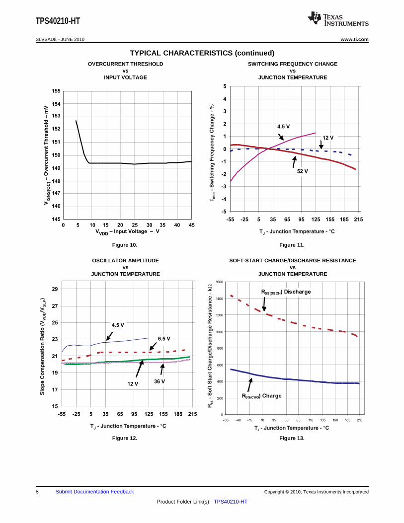
TYPICAL CHARACTERISTICS (continued)OVERCURRENT THRESHOLD SWITCHING FREQUENCY CHANGE
vs vsINPUT VOLTAGE JUNCTION TEMPERATURE
Figure 10. Figure 11.
OSCILLATOR AMPLITUDE SOFT-START CHARGE/DISCHARGE RESISTANCEvs vs
JUNCTION TEMPERATURE JUNCTION TEMPERATURE
Figure 12. Figure 13.
8 Submit Documentation Feedback Copyright © 2010, Texas Instruments Incorporated
Product Folder Link(s): TPS40210-HT

T - Junction Temperature - °CJ
I-
Feed
back B
ias C
urr
en
t -
nA
IB(F
B)
0
20
40
60
80
100
120
140
160
180
-55 -25 5 35 65 95 125 155 185 215
T - Junction Temperature - °CJ
I-
Co
mp
en
sati
on
So
urc
e C
urr
en
t -
µA
CO
MP
(SR
C)
0
50
10 0
150
2 0 0
2 50
3 0 0
- 55 - 2 5 5 3 5 6 5 9 5 12 5 155 18 5 2 15
T - Junction Temperature - °CJ
I-
Co
mp
en
sa
tio
n S
ink
Cu
rre
nt
- m
AC
OM
P(S
NK
)
0
1
2
3
4
5
-55 -25 5 35 65 95 125 155 185 215
T - Junction Temperature - °CJ
V-V
all
ey
Vo
ltag
e C
ha
ng
e -
%V
LY
-6
-5
-4
-3
-2
-1
0
1
2
3
-55 -25 5 35 65 95 125 155 185 215
TPS40210-HT
www.ti.com SLVSAD8 –JUNE 2010
TYPICAL CHARACTERISTICS (continued)FB BIAS CURRENT COMPENSATION SOURCE CURRENT
vs vsJUNCTION TEMPERATURE JUNCTION TEMPERATURE
Figure 14. Figure 15.
COMPENSATION SINK CURRENT VALLEY VOLTAGE CHANGEvs vs
JUNCTION TEMPERATURE JUNCTION TEMPERATURE
Figure 16. Figure 17.
Copyright © 2010, Texas Instruments Incorporated Submit Documentation Feedback 9
Product Folder Link(s): TPS40210-HT

7.4
7.6
7.8
8
8.2
8.4
8.6
8.8
9
-65 -40 -15 10 35 60 85 110 135 160 185 210
ILOAD = 0 mA
ILOAD = 5 mA
T - Junction Temperature - °CJ
V-
Reg
ula
tor
Vo
ltag
e -
VB
P
T - Junction Temperature - °CJ
V-
DIS
/EN
Tu
rn-O
nT
hre
sh
old
-V
DIS
(EN
)–
–1
1.02
1.04
1.06
1.08
1.1
1.12
1.14
1.16
1.18
1.2
-55 -25 5 35 65 95 125 155 185 215
T - Junction Temperature - °CJ
A-
Cu
rren
t S
en
se A
mp
lifi
er
Gain
-V
/VC
S
0
1
2
3
4
5
6
7
-55 -25 5 35 65 95 125 155 185 215
TPS40210-HT
SLVSAD8 –JUNE 2010 www.ti.com
TYPICAL CHARACTERISTICS (continued)REGULATOR VOLTAGE DIS/EN TURN-ON THRESHOLD
vs vsJUNCTION TEMPERATURE JUNCTION TEMPERATURE
Figure 18. Figure 19.
CURRENT SENSE AMPLIFIER GAINvs
JUNCTION TEMPERATURE
Figure 20.
10 Submit Documentation Feedback Copyright © 2010, Texas Instruments Incorporated
Product Folder Link(s): TPS40210-HT

1
65
10
2
3
74
8
9
FB
RC
COMP
DIS/EN
SS
GND
VDD
ISNS
GDRV
BP
DGQ PowerPAD PACKAGE
(Top View)HKK PACKAGE
(TOP VIEW)
TPS40210-HT
www.ti.com SLVSAD8 –JUNE 2010
DEVICE INFORMATION
TERMINAL FUNCTIONSTERMINAL
I/O DESCRIPTIONNAME NO.
BP 9 O Regulator output. Connect a 1.0-mF bypass capacitor from this pin to GND.
COMP 4 O Error amplifier output. Connect control loop compensation network between COMP pin and FB pin.
Disable/enable. Pulling this pin high places the part into a shutdown mode. Shutdown mode is characterizedby a very low quiescent current. While in shutdown mode, the functionality of all blocks is disabled, and theDIS/EN 3 I BP regulator is shut down. This pin has an internal 1-MΩ pulldown resistor to GND. Leaving this pinunconnected enables the device.
Error amplifier inverting input. Connect a voltage divider from the output to this pin to set the output voltage.FB 5 I Compensation network is connected between this pin and COMP.
GDRV 8 O Connect the gate of the power N-channel MOSFET to this pin.
GND 6 – Device ground
Current sense. Connect an external current sensing resistor between this pin and GND. The voltage on thispin is used to provide current feedback in the control loop and detect an overcurrent condition. AnISNS 7 I overcurrent condition is declared when ISNS pin voltage exceeds the overcurrent threshold voltage, 150 mVtypical.
Switching frequency setting. Connect capacitor from RC pin to GND. Connect a resistor from RC pin to VDDRC 1 I of the IC power supply and a capacitor from RC to GND.
Soft-start time programming. Connect capacitor from SS pin to GND to program converter soft-start time.SS 2 I This pin also functions as a timeout timer when the power supply is in an overcurrent condition.
System input voltage. Connect a local bypass capacitor from this pin to GND. Depending on the amount ofVDD 10 I required slope compensation, this pin can be connected to the converter output. See Application Information
section for additional details.
Copyright © 2010, Texas Instruments Incorporated Submit Documentation Feedback 11
Product Folder Link(s): TPS40210-HT

++
Soft Start
and
Overcurrent
5FB
4COMP
3DIS/EN
700 mVLDO
PWM
Logic
2SS
1RC
Oscillator
and
Slope
Compensation
UVLO
Driver
9 BP
10 VDD
8 GDRV
6 GND
7 ISNS
+Gain = 6
+
150 mV
LEB
OC Fault
OC Fault
UDG-07107
Enable E/A
E/A
SS Ref
TPS40210-HT
SLVSAD8 –JUNE 2010 www.ti.com
FUNCTIONAL BLOCK DIAGRAM
12 Submit Documentation Feedback Copyright © 2010, Texas Instruments Incorporated
Product Folder Link(s): TPS40210-HT
OUT D
IN
V V 1
V 1 D
+
=
-
IN
OUT D
VD 1
V V
æ öæ ö= -ç ÷ç ÷ç ÷+è øè ø
( )
( )
fOUT D OUT SW
2
IN
2 V V I LD
V
´ + ´ ´ ´=
( ) ( )
( ) f
2OUT D IN IN
OUT(crit) 2OUT D SW
V V V VI
2 V V L
+ - ´=
´ + ´ ´
TPS40210-HT
www.ti.com SLVSAD8 –JUNE 2010
APPLICATION INFORMATION
Minimum On-Time and Off-Time Considerations
The TPS40210 has a minimum off time of approximately 200 ns and a minimum on time of 300 ns. These twoconstraints place limitations on the operating frequency that can be used for a given input-to-output conversionratio. See Figure 3 for the maximum frequency that can be used for a given duty cycle.
The duty cycle at which the converter operates is dependent on the mode in which the converter is running. If theconverter is running in discontinuous conduction mode, the duty cycle varies with changes to the load muchmore than it does when running in continuous conduction mode.
In continuous conduction mode, the duty cycle is related primarily to the input and output voltages.
(1)
(2)
In discontinuous mode, the duty cycle is a function of the load, input and output voltages, inductance, andswitching frequency.
(3)
All converters using a diode as the freewheeling or catch component have a load current level at which theytransition from discontinuous conduction to continuous conduction. This is the point at which the inductor currentfalls to zero. At higher load currents, the inductor current does not fall to zero but remains flowing in a positivedirection and assumes a trapezoidal wave shape as opposed to a triangular wave shape. This load boundarybetween discontinuous conduction and continuous conduction can be found for a set of converter parameters asshown in Equation 4.
(4)
For loads higher than the result of Equation 4, the duty cycle is given by Equation 2, and for loads less than theresults of Equation 4, the duty cycle is given Equation 3. For Equation 1 through Equation 4, the variabledefinitions are as follows:• VOUT is the output voltage of the converter in V• VD is the forward conduction voltage drop across the rectifier or catch diode in V• VIN is the input voltage to the converter in V• IOUT is the output current of the converter in A• L is the inductor value in H• f SW is the switching frequency in Hz
Copyright © 2010, Texas Instruments Incorporated Submit Documentation Feedback 13
Product Folder Link(s): TPS40210-HT

T 8 10 2 7 4 6 9 2SW T SW SW T T
1R
5.8 10 f C 8 10 f 1.4 10 f 1.5 10 1.7 10 C 4 10 C- - - - - -
=
´ ´ ´ + ´ ´ + ´ ´ - ´ + ´ ´ - ´ ´
+
1
RC
150 mV
S Q
QR
+
+
8
5
VDD
GND
RRC
CRC
CLK
External Frequency
Synchronization
(optional)
VIN
TPS40210/11
UDG-08063
10
1
6
TPS40210-HT
SLVSAD8 –JUNE 2010 www.ti.com
Setting the Oscillator Frequency
The oscillator frequency is determined by a resistor and capacitor connected to the RC pin of the TPS40210. Thecapacitor is charged to a level of approximately VVDD/20 by current flowing through the resistor and is thendischarged by a transistor internal to the TPS40210. The required resistor for a given oscillator frequency isfound from either Figure 2 or Equation 5.
where• RT is the timing resistance in kΩ• f SW is the switching frequency in kHz• CT is the timing capacitance in pF (5)
For most applications, a capacitor in the range of 68 pF to 120 pF gives the best results. Resistor values shouldbe limited to between 100 kΩ and 1 MΩ as well. If the resistor value falls below 100 kΩ, decrease the capacitorsize and recalculate the resistor value for the desired frequency. As the capacitor size decreases below 47 pF,the accuracy of Equation 5 degrades, and empirical means may be needed to fine tune the timing componentvalues to achieve the desired switching frequency.
Synchronizing the Oscillator
The TPS40210 can be synchronized to an external clock source. Figure 21 shows the functional diagram of theoscillator. When synchronizing the oscillator to an external clock, the RC pin must be pulled below 150 mV for 20ns or more. The external clock frequency must be higher than the free running frequency of the converter aswell. When synchronizing the controller, if the RC pin is held low for an excessive amount of time, erraticoperation may occur. The maximum amount of time that the RC pin should be held low is 50% of a nominaloutput pulse, or 10% of the period of the synchronization frequency.
Under circumstances where the duty cycle is less than 50%, a Schottky diode connected from the RC pin to anexternal clock may be used to synchronize the oscillator. The cathode of the diode is connected to the RC pin.The trip point of the oscillator is set by an internal voltage divider to be 1/20 of the input voltage. The clock signalmust have an amplitude higher than this trip point. When the clock goes low, it allows the reset current to restartthe RC ramp, synchronizing the oscillator to the external clock. This provides a simple single-component methodfor clock synchronization.
Figure 21. Oscillator Functional Diagram
14 Submit Documentation Feedback Copyright © 2010, Texas Instruments Incorporated
Product Folder Link(s): TPS40210-HT

+
1
RC
TPS40210/11
150 mV
S Q
QR
+
+
8
5
VDD
GND
RRC
CRC
CLK
Frequency > Controller
Frequency
VIN
Amplitude >20
VIN
Duty Cycle < 50%
UDG-08064
10
1
6
10
1
6
TPS40210/11
VDD
RC
GND
CT
RT
UDG-07119
10
8
7
VDD
ISNS
GDRV
GND
TPS40210/11
L
VOUT
VIN
6
RISNS
UDG-07120
CIFLT
RIFLT
TPS40210-HT
www.ti.com SLVSAD8 –JUNE 2010
Figure 22. Diode Connected Synchronization
Current Sense and Overcurrent
The TPS40210 are current-mode controllers and use a resistor in series with the source terminal power FET tosense current for both the current-mode control and overcurrent protection. The device enters a current-limitstate if the voltage on the ISNS pin exceeds the current-limit threshold voltage VISNS(oc) from the electricalspecifications table. When this happens, the controller discharges the SS capacitor through a relatively highimpedance and then attempts to restart. The amount of output current that causes this to happen is dependenton several variables in the converter.
Figure 23. Oscillator Components Figure 24. Current Sense Components
Copyright © 2010, Texas Instruments Incorporated Submit Documentation Feedback 15
Product Folder Link(s): TPS40210-HT

( )
f
f
SW ISNS(oc)ISNS
SW OUT(oc) OUT D IN
L VR
2 L I V V V
´ ´=
´ ´ ´ ´ + -
( ) f
ISNS ISNSISNS
OUT RIPPLE OUT IN
SW
V VR
I I I D V
1 D 2 1 D 2 L
= =æ ö æ öæ ö æ ö´+ +ç ÷ ç ÷ç ÷ ç ÷ç ÷- è ø - ´ ´è ø è øè ø
fVDD
e SW
Vs
20
æ ö= ´ ç ÷
è ø
( )CS ISNS OUT D INA R V V Vm2
L
´ ´ + -=
TPS40210-HT
SLVSAD8 –JUNE 2010 www.ti.com
The load current overcurrent threshold is set by proper choice of RISNS. If the converter is operating indiscontinuous mode the current sense resistor is found in Equation 6.
(6)
If the converter is operating in continuous conduction mode RISNS can be found in Equation 7.
where• RISNS is the value of the current sense resistor in Ω.• VISNS(oc) is the overcurrent threshold voltage at the ISNS pin (from electrical specifications)• D is the duty cycle (from Equation 2)• f SW is the switching frequency in Hz• VIN is the input voltage to the power stage in V (see text)• L is the value of the inductor in H• IOUT(oc) is the desired overcurrent trip point in A• VD is the drop across the diode in Figure 24 (7)
The TPS40210 have a fixed undervoltage lockout (UVLO) that allows the controller to start at a typical inputvoltage of 4.25 V. If the input voltage is slowly rising, the converter might have less than its designed nominalinput voltage available when it has reached regulation. As a result, this may decreases the apparent current-limitload current value and must be taken into consideration when selecting RISNS. The value of VIN used to calculateRISNS must be the value at which the converter finishes startup. The total converter output current at startup isthe sum of the external load current and the current required to charge the output capacitor(s). See the Soft Startsection of this data sheet for information on calculating the required output capacitor charging current.
The topology of the standard boost converter has no method to limit current from the input to the output in theevent of a short circuit fault on the output of the converter. If protection from this type of event is desired, it isnecessary to use some secondary protection scheme such as a fuse or rely on the current limit of the upstreampower source.
Current Sense and Sub-Harmonic Instability
A characteristic of peak current-mode control results in a condition where the current control loop can exhibitinstability. This results in alternating long and short pulses from the pulse-width modulator. The voltage loopmaintains regulation and does not oscillate, but the output ripple voltage increases. The condition occurs onlywhen the converter is operating in continuous conduction mode, and the duty cycle is 50% or greater. The causeof this condition is described in Texas Instruments literature number SLUA101, available at www.ti.com. Theremedy for this condition is to apply a compensating ramp from the oscillator to the signal going to thepulse-width modulator. In the TPS40210, the oscillator ramp is applied in a fixed amount to the pulse-widthmodulator. The slope of the ramp is given in Equation 8.
(8)
To ensure that the converter does not enter into sub-harmonic instability, the slope of the compensating rampsignal must be at least half of the down slope of the current ramp signal. Because the compensating ramp isfixed in the TPS40210, this places a constraint on the selection of the current sense resistor.
The down slope of the current sense wave form at the pulse-width modulator is described in Equation 9.
(9)
16 Submit Documentation Feedback Copyright © 2010, Texas Instruments Incorporated
Product Folder Link(s): TPS40210-HT

( )fVDD SW
ISNS(max)OUT D IN
V LR
60 V V V
´ ´=
´ + -
fON
SW
Dt =
IFLT IFLT ONR C 0.1 t´ = ´
TPS40210-HT
www.ti.com SLVSAD8 –JUNE 2010
Since the slope compensation ramp must be at least half, and preferably equal to the down slope of the currentsense waveform seen at the pulse-width modulator, a maximum value is placed on the current sense resistorwhen operating in continuous mode at 50% duty cycle or greater. For design purposes, some margin should beapplied to the actual value of the current sense resistor. As a starting point, the actual resistor chosen should be80% or less that the value calculated in Equation 10. This equation calculates the resistor value that makes theslope compensation ramp equal to one half of the current ramp downslope. Values no more than 80% of thisresult are acceptable.
where• Se is the slope of the voltage compensating ramp applied to the pulse-width modulator in V/s• f SW is the switching frequency in Hz• VVDD is the voltage at the VDD pin in V• m2 is the down slope of the current sense waveform seen at the pulse-width modulator in V/s• RISNS is the value of the current sense resistor in Ω• VOUT is the converter output voltage VIN is the converter power stage input voltage• VD is the drop across the diode in Figure 24 (10)
It is possible to increase the voltage compensation ramp slope by connecting the VDD pin to the output voltageof the converter instead of the input voltage as shown in Figure 24. This can help in situations where theconverter design calls for a large ripple current value in relation to the desired output current limit setting.
NOTEConnecting the VDD pin to the output voltage of the converter affects the startup voltageof the converter since the controller undervoltage lockout (UVLO) circuit monitors the VDDpin and senses the input voltage less the diode drop before startup. The effect is toincrease the startup voltage by the value of the diode voltage drop.
If an acceptable RISNS value is not available, the next higher value can be used and the signal from the resistordivided down to an acceptable level by placing another resistor in parallel with CISNS.
Current Sense Filtering
In most cases, a small filter placed on the ISNS pin improves performance of the converter. These are thecomponents RIFLT and CIFLT in Figure 24. The time constant of this filter should be approximately 10% of thenominal pulse width of the converter. The pulse width can be found using Equation 11.
(11)
The suggested time constant is then
(12)
The range of RIFLT should be from about 1 kΩ to 5 kΩ for best results. Higher values can be used, but this raisesthe impedance of the ISNS pin connection more than necessary and can lead to noise-pickup issues in somelayouts. CISNS should be located as close as possible to the ISNS pin as well to provide noise immunity.
Soft Start
The soft-start feature of the TPS40210 is a closed-loop soft start, meaning that the output voltage follows a linearramp that is proportional to the ramp generated at the SS pin. This ramp is generated by an internal resistorconnected from the BP pin to the SS pin and an external capacitor connected from the SS pin to GND. The SSpin voltage (VSS) is level shifted down by approximately VSS(ofst) (approximately 1 V) and sent to one of the “+”inputs (the “+” input with the lowest voltage dominates) of the error amplifier. When this level-shifted voltage(VSSE) starts to rise at time t1 (see Figure 25), the output voltage that the controller expects rises as well. SinceVSSE starts at near 0 V, the controller attempts to regulate the output voltage from a starting point of zero volts. It
Copyright © 2010, Texas Instruments Incorporated Submit Documentation Feedback 17
Product Folder Link(s): TPS40210-HT

VSSE(1)
VSS
VOUT
VSSE
VSS(ofst)
t0
t1
VSS(ofst)
+700 mV
VIN
- VD
t2
t3
2
5
4
SS
COMP
FB
TPS40210/11
RSS(chg)
UDG-07121
++
RSS(dchg)
700 mV REF
OC Fault
UVLODIS
Error Amplifier
TPS40210-HT
SLVSAD8 –JUNE 2010 www.ti.com
cannot do this, due to the converter architecture. The output voltage starts from the input voltage less the dropacross the diode (VIN – VD) and rises from there. The point at which the output voltage starts to rise (t2) is whenthe VSSE ramp passes the point where it is commanding more output voltage than (VIN – VD). This voltage level islabeled VSSE(1). The time required for the output voltage to ramp from a theoretical zero to the final regulatedvalue (from t1 to t3) is determined by the time it takes for the capacitor connected to the SS pin (CSS) to risethrough a 700-mV range, beginning at VSS(ofst) above GND.
Figure 25. SS Pin Voltage and Output Voltage Figure 26. SS Pin Functional Circuit
18 Submit Documentation Feedback Copyright © 2010, Texas Instruments Incorporated
Product Folder Link(s): TPS40210-HT

( )
SSSS
BP SS(ofst)SS
BP SS(ofst) FB
tC
V VR ln
V V V
=æ ö-ç ÷´ç ÷- +è ø
I =C(chg)
C V
tOUT OUT
SS
´
t >SS
C V
(I I )OUT OUT
OUT(oc) EXT-
´
TPS40210-HT
www.ti.com SLVSAD8 –JUNE 2010
The required capacitance for a given soft start time t3 – t1 in Figure 25 is calculated in Equation 13.
where• tSS is the soft-start time• RSS(chg) is the SS charging resistance in Ω, typically 500 kΩ• CSS is the value of the capacitor on the SS pin, in F• VBP is the value of the voltage on the BP pin in V• VSS(ofst) is the approximate level shift from the SS pin to the error amplifier (~1 V)• VFB is the error amplifier reference voltage, 700 mV typical (13)
Note that tSS is the time it takes for the output voltage to rise from 0 V to the final output voltage. Also note thetolerance on RSS(chg) given in the electrical specifications table. This contributes to some variability in the outputvoltage rise time, and margin must be applied to account for it in design.
Also take note of VBP. Its value varies depending on input conditions. For example, a converter operating from aslowly rising input initializes VBP at a fairly low value and increases during the entire startup sequence. If thecontroller has a voltage above 8 V at the input and the DIS pin is used to stop and then restart the converter, VBPis approximately 8 V for the entire startup sequence. The higher the voltage on BP, the shorter the startup time isand conversely, the lower the voltage on BP, the longer the startup time is.
The soft-start time (tSS) must be chosen long enough so that the converter can start up without going into anovercurrent state. Since the overcurrent state is triggered by sensing the peak voltage on the ISNS pin, thatvoltage must be kept below the overcurrent threshold voltage VISNS(oc). The voltage on the ISNS pin is a functionof the load current of the converter, the rate of rise of the output voltage and the output capacitance, and thecurrent sensing resistor. The total output current that must be supported by the converter is the sum of thecharging current required by the output capacitor and any external load that must be supplied during startup. Thiscurrent must be less than the IOUT(oc) value used in Equation 6 or Equation 7 (depending on the operating modeof the converter) to determine the current sense resistor value.
In these equations, the actual input voltage at the time that the controller reaches the final output voltage is theimportant input voltage to use in the calculations. If the input voltage is slowly rising and is at less than thenominal input voltage when the startup time ends, the output current limit is less than IOUT(oc) at the nominal inputvoltage. The output capacitor charging current must be reduced (decrease COUT or increase the tSS) or IOUT(oc)must be increased and a new value for RISNS calculated.
(14)
where• IC(chg) is the output capacitor charging current in A• COUT is the total output capacitance in F• VOUT is the output voltage in V• tSS is the soft start time from Equation 13• IOUT(oc) is the desired over current trip point in A• IEXT is any external load current in A (15)
Copyright © 2010, Texas Instruments Incorporated Submit Documentation Feedback 19
Product Folder Link(s): TPS40210-HT

SS(ofst)DCHG SS(dchg) SS
SS(rst)
Vt R C ln
V
æ öç ÷= ´ ´ç ÷è ø
( )( )
BP SS(rst)
CHG SS(chg) SS
BP SS(ofst)
V Vt R C ln
V V
æ ö-ç ÷= ´ ´ç ÷-è ø
( ) CHG DCHGRSTRT mint t t= +
tRSTR(min)
VSS(ofst)
VSS
VBP
VSS(rst)
T - Time
TPS40210-HT
SLVSAD8 –JUNE 2010 www.ti.com
The capacitor on the SS pin (CSS) also plays a role in overcurrent functionality. It is used as the timer betweenrestart attempts. The SS pin is connected to GND through a resistor, RSS(dchg), when the controller senses anovercurrent condition. Switching stops and nothing else happens until the SS pin discharges to the soft-startreset threshold, VSS(rst). At this point, the SS pin capacitor is allowed to charge again through the chargingresistor RSS(chg), and the controller restarts from that point. The shortest time between restart attempts occurswhen the SS pin discharges from VSS(ofst) (approximately 1 V) to VSS(rst) (150 mV) and then back to VSS(ofst) andswitching resumes. In actuality, this is a conservative estimate since switching does not resume until the VSSEramp rises to a point where it is commanding more output voltage than exists at the output of the controller. Thisoccurs at some SS pin voltage greater than VSS(ofst) and depends on the voltage that remains on the outputovervoltage the converter while switching has been halted. The fastest restart time can be calculated by usingEquation 16, Equation 17, and Equation 18.
(16)
(17)
(18)
Figure 27. Soft Start During Overcurrent
20 Submit Documentation Feedback Copyright © 2010, Texas Instruments Incorporated
Product Folder Link(s): TPS40210-HT
Q VDD VDD(en)P V I= ´
fG VDD g SWP V Q= ´ ´
E VDD EXTP V I= ´
TPS40210-HT
www.ti.com SLVSAD8 –JUNE 2010
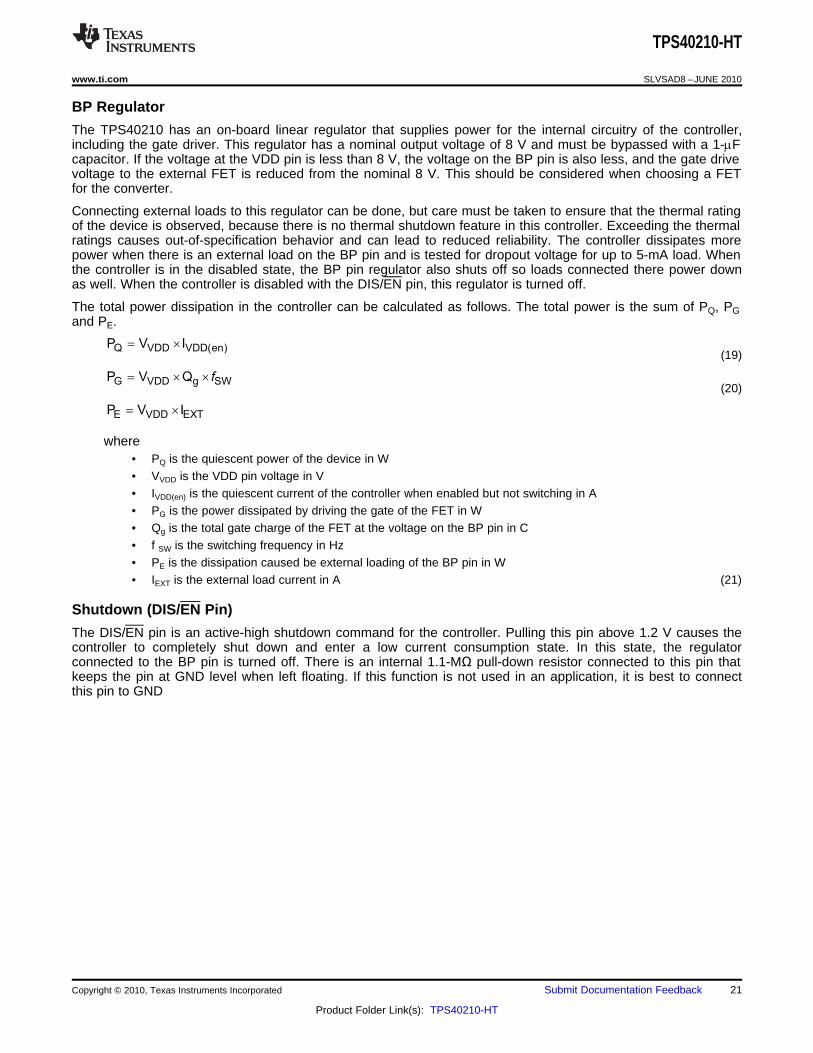
BP Regulator
The TPS40210 has an on-board linear regulator that supplies power for the internal circuitry of the controller,including the gate driver. This regulator has a nominal output voltage of 8 V and must be bypassed with a 1-mFcapacitor. If the voltage at the VDD pin is less than 8 V, the voltage on the BP pin is also less, and the gate drivevoltage to the external FET is reduced from the nominal 8 V. This should be considered when choosing a FETfor the converter.
Connecting external loads to this regulator can be done, but care must be taken to ensure that the thermal ratingof the device is observed, because there is no thermal shutdown feature in this controller. Exceeding the thermalratings causes out-of-specification behavior and can lead to reduced reliability. The controller dissipates morepower when there is an external load on the BP pin and is tested for dropout voltage for up to 5-mA load. Whenthe controller is in the disabled state, the BP pin regulator also shuts off so loads connected there power downas well. When the controller is disabled with the DIS/EN pin, this regulator is turned off.
The total power dissipation in the controller can be calculated as follows. The total power is the sum of PQ, PGand PE.
(19)
(20)
where• PQ is the quiescent power of the device in W• VVDD is the VDD pin voltage in V• IVDD(en) is the quiescent current of the controller when enabled but not switching in A• PG is the power dissipated by driving the gate of the FET in W• Qg is the total gate charge of the FET at the voltage on the BP pin in C• f SW is the switching frequency in Hz• PE is the dissipation caused be external loading of the BP pin in W• IEXT is the external load current in A (21)
Shutdown (DIS/EN Pin)
The DIS/EN pin is an active-high shutdown command for the controller. Pulling this pin above 1.2 V causes thecontroller to completely shut down and enter a low current consumption state. In this state, the regulatorconnected to the BP pin is turned off. There is an internal 1.1-MΩ pull-down resistor connected to this pin thatkeeps the pin at GND level when left floating. If this function is not used in an application, it is best to connectthis pin to GND
Copyright © 2010, Texas Instruments Incorporated Submit Documentation Feedback 21
Product Folder Link(s): TPS40210-HT

1
2
3
4
10
9
8
7
RC
DIS/EN
COMP
SS
VDD
ISNS
GDRV
GND
TPS40210
CFB
L
COUT
ROUT
VOUT
VIN
5 FB 6
BP
RFB
RSENSE
UDG-07177
RIFLT
CIFLT
CHF
R1
R2
( )fCO M OUT COAK g Z 19.1 0.146 2.80
V= ´ = ´ W =
( ) ( ) ( ) ( )
f
f
SW
OUTM 2 2
ISNS ISNS SW
600kHz0.13 L 0.13 10 H
R 240 Ag 19.1V
12m 120 12m 10 H 600kHzR 120 R L
´ ´ ´ m ´W
= = =W ´ ´ W + m ´´ ´ + ´
TPS40210-HT
SLVSAD8 –JUNE 2010 www.ti.com
Control Loop Considerations
There are two methods to design a suitable control loop for the TPS40210. The first (and preferred, if equipmentis available) is to use a frequency-response analyzer to measure the open-loop modulator and power stage gainand to then design compensation to fit that. The usage of these tools for this purpose is well documented withthe literature that accompanies the tool and is not discussed here.
The second option is to make an initial guess at compensation, and then evaluate the transient response of thesystem to see if the compensation is acceptable to the application or not. For most systems, an adequateresponse can be obtained by simply placing a series resistor and capacitor (RFB and CFB) from the COMP pin tothe FB pin as shown in Figure 28.
Figure 28. Basic Compensation Network
The natural phase characteristics of most capacitors used for boost outputs combined with the current modecontrol provide adequate phase margin when using this type of compensation. To determine an initial startingpoint for the compensation, the desired crossover frequency must be considered when estimating the control tooutput gain. The model used is a current source into the output capacitor and load.
When using these equations, the loop bandwidth should be no more than 20% of the switching frequency, f SW. Amore reasonable loop bandwidth would be 10% of the switching frequency. Be sure to evaluate the transientresponse of the converter over the expected load range to ensure acceptable operation.
(22)
(23)
22 Submit Documentation Feedback Copyright © 2010, Texas Instruments Incorporated
Product Folder Link(s): TPS40210-HT

( )( )( ) ( )( ) ( )
2
L ESR OUT
OUT OUT2 2 2
OUT OUT ESR ESR L OUT
1 2 f R C
Z R
1 R 2 R R R 2 f C
+ p ´ ´ ´
= ´
+ + ´ ´ + ´ p ´ ´
COMP
CO
1 1K 0.356
K 2.80= = =
FB COMP
CO
R1R R1 K
K= = ´
FB
L FB
10C
2 f R=
p ´ ´
HF
L FB
1C
20 f R=
p ´ ´
TPS40210-HT
www.ti.com SLVSAD8 –JUNE 2010
where• KCO is the control to output gain of the converter, in V/V• gM is the transconductance of the power stage and modulator, in S• ROUT is the output load equivalent resistance, in Ω• ZOUT is the output impedance, including the output capacitor, in Ω• RISNS is the value of the current sense resistor, in Ω• L is the value of the inductor, in H• COUT is the value of the output capacitance, in mF• RESR is the equivalent series resistance of COUT, in Ω• f SW is the switching frequency, in Hz• f L is the desired crossover frequency for the control loop, in Hz (24)
These equations assume that the operation is discontinuous and that the load is purely resistive. The gain incontinuous conduction can be found by evaluating Equation 23 at the resistance that gives the critical conductioncurrent for the converter. Loads that are more like current sources give slightly higher gains than predicted here.To find the gain of the compensation network required for a control loop of bandwidth f L, take the reciprocal ofEquation 22.
(25)
The GBWP of the error amplifier is only specified to be at least 1.5 MHz. If KCOMP multiplied by the fL is greaterthan 750 kHz, reduce the desired loop crossover frequency until this condition is satisfied. This ensures that thehigh-frequency pole from the error amplifier response with the compensation network in place does not causeexcessive phase lag at the f L and decrease phase margin in the loop.
The R-C network connected from COMP to FB places a zero in the compensation response. That zero should beapproximately 1/10th of the desired crossover frequency, f L. With that being the case, RFB and CFB can be foundfrom Equation 26 and Equation 27
(26)
where• R1 is in fL is the loop crossover frequency desired, in Hz.• RFB is the feedback resistor in CFB is the feedback capacitance in mF. (27)
Thought not strictly necessary, it is recommended that a capacitor be added between COMP and FB to providehigh-frequency noise attenuation in the control loop circuit. This capacitor introduces another pole in thecompensation response. The allowable location of that pole frequency determines the capacitor value. As astarting point, the pole frequency should be 10 × fL. The value of CHF can be found from Equation 28.
(28)
Copyright © 2010, Texas Instruments Incorporated Submit Documentation Feedback 23
Product Folder Link(s): TPS40210-HT
( )HF 6
FB
1C
2 1.5 10 R
=p ´ ´ ´
G
G
105R
Q=
10
8
7
6
VDD
GDRV
ISNS
GND
TPS40210/11 L
VIN
RG
VOUT
UDG-07196
TPS40210-HT
SLVSAD8 –JUNE 2010 www.ti.com
The error amplifier GBWP will usually be higher, but is ensured by design to be at least 1.5 MHz. If the gainrequired in Equation 25 multiplied by 10 times the desired control loop crossover frequency, the high-frequencypole introduced by CHF is overridden by the error amplifier capability and the effective pole is lower in frequency.If this is the case, CHF can be made larger to provide a consistent high-frequency roll off in the control loopdesign. Equation 29 calculates the required CHF in this case.
where• CHF is the high-frequency roll-off capacitor value in mF• RFB is the mid-band gain-setting resistor value in Ω (29)
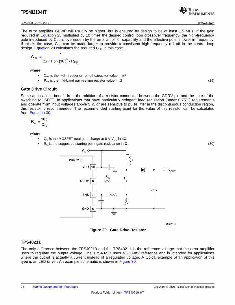
Gate Drive Circuit
Some applications benefit from the addition of a resistor connected between the GDRV pin and the gate of theswitching MOSFET. In applications that have particularly stringent load regulation (under 0.75%) requirementsand operate from input voltages above 5 V, or are sensitive to pulse jitter in the discontinuous conduction region,this resistor is recommended. The recommended starting point for the value of this resistor can be calculatedfrom Equation 30.
where• QG is the MOSFET total gate charge at 8-V VGS in nC.• RG is the suggested starting point gate resistance in Ω. (30)
Figure 29. Gate Drive Resistor
TPS40211
The only difference between the TPS40210 and the TPS40211 is the reference voltage that the error amplifieruses to regulate the output voltage. The TPS40211 uses a 260-mV reference and is intended for applicationswhere the output is actually a current instead of a regulated voltage. A typical example of an application of thistype is an LED driver. An example schematic is shown in Figure 30.
24 Submit Documentation Feedback Copyright © 2010, Texas Instruments Incorporated
Product Folder Link(s): TPS40210-HT

10
9
8
7
VDD
BP
ISNS
GDRV
TPS40210/11 L
VIN
UDG-07197
6GND
RIFB
1
2
3
4
5
RC
SS
COMP
DIS/EN
FB
IOUT
FBIFB
OUT
VR
I=
TPS40210-HT
www.ti.com SLVSAD8 –JUNE 2010
Figure 30. Typical LED Drive Schematic
The current in the LED string is set by the choice of the resistor RISNS as shown in Equation 31.
where• RIFB is the value of the current sense resistor for the LED string in Ω.• VFB is the reference voltage for the TPS40211 in V (0.260 V typ).• IOUT is the desired DC current in the LED string in A. (31)
Copyright © 2010, Texas Instruments Incorporated Submit Documentation Feedback 25
Product Folder Link(s): TPS40210-HT

TPS40210-HT
SLVSAD8 –JUNE 2010 www.ti.com
ADDITIONAL REFERENCES
References
These references may be found on the web at www.power.ti.com under Technical Documents. Many designtools and links to additional references, may also be found at www.power.ti.com1. Design and Application Guide for High Speed MOSFET Gate Drive Circuits, SEM 1400, 2001 Seminar
Series2. Designing Stable Control Loops, SEM 1400, 2001 Seminar Series3. Additional PowerPADTM information may be found in Applications Briefs SLMA002 and SLMA0044. QFN/SON PCB Attachment, Texas Instruments Literature Number SLUA271, June 2002
26 Submit Documentation Feedback Copyright © 2010, Texas Instruments Incorporated
Product Folder Link(s): TPS40210-HT

+
+
TPS40210-HT
www.ti.com SLVSAD8 –JUNE 2010
DESIGN EXAMPLE 1
12-V to 24-V Non-Synchronous Boost Regulator
The following example illustrates the design process and component selection for a 12-V to 24-Vnon-synchronous boost regulator using the TPS40210 controller.
Figure 31. TPS40210 Design Example – 8-V to 24-V at 2-A
Table 2. TPS40210 Design Example Specifications
PARAMETER CONDITIONS MIN NOM MAX UNIT
INPUT CHARACTERISTICS
VIN Input voltage 8 12 14 V
IIN Input current 4.4A
No load input current 0.05
VIN(UVLO) Input undervoltage lockout 4.5 V
OUTPUT CHARACTERISTICS
VOUT Output voltage 23.5 24.0 24.5 V
Line regulation 1%
Load regulation 1%
VOUT(ripple) Output voltage ripple 500 mVPP
IOUT Output current 8 V ≤ VIN ≤ 14 V 0.2 1 2A
IOCP Output overcurrent inception point 3.5
Transient response
ΔI Load step 1 A
Load slew rate 1 A/ms
Overshoot threshold voltage 500 mV
Settling time 5 ms
Copyright © 2010, Texas Instruments Incorporated Submit Documentation Feedback 27
Product Folder Link(s): TPS40210-HT

OUT IN(max) FDMIN
OUT FD
V V V 24 V 14 V 0.5 VD 42.8%
V V 24 V 0.5 V
- + - +» = =
+ +
OUT IN(min) FDMAX
OUT FD
V V V 24 V 8 V 0.5 VD 67.3%
V V 24 V 0.5 V
- + - +» = =
+ +
OUT(max)Lrip(max)
MIN
I 2I 0.3 0.3 1.05 A
1 D 1 0.428= ´ = ´ =
- -
IN(max)MIN MIN
Lrip(max) SW
V 1 14 V 1L » D 0.428 9.5 H
I f 1.05 A 600kHz´ ´ = ´ ´ = m
f
INRIPPLE
SW
V 1 12 V 1I D 0.50 1.02 A
L 10 H 600kHz» ´ ´ = ´ ´ =
m
f
INRIPPLE(Vinmin)
SW
V 1 8 V 1I D 0.673 0.89 A
L 10 H 600kHz» ´ ´ = ´ ´ =
m
( )( ) ( ) ( ) ( )( )2 22 222 OUT(max)1 1 1
Lrms RIPPLE RIPPLE(VINmin)L avg 12 12 12MAX
I 2I I I I 0.817A 6.13 Arms
1 D 1 0.673
æ ö æ ö= + » + = + ´ =ç ÷ ç ÷ç ÷- -è øè ø
TPS40210-HT
SLVSAD8 –JUNE 2010 www.ti.com
Table 2. TPS40210 Design Example Specifications (continued)
PARAMETER CONDITIONS MIN NOM MAX UNIT
SYSTEM CHARACTERISTICS
fSW Switching frequency 600 kHz
hPK Peak efficiency VIN = 12 V, 0.2 A ≤ IOUT ≤ 2 A 95%
h Full load efficiency VIN = 12 V, IOUT = 2 A 94%
TOP Operating temperature range 10 V ≤ VIN ≤ 14 V, 0.2 A ≤ IOUT ≤ 2 A 25 °C
MECHANICAL DIMENSIONS
W Width 1.5
L Length 1.5 in
h Height 0.5
Step-By-Step Design Procedure
Duty Cycle Estimation
The duty cycle of the main switching MOSFET is estimated using Equation 32 and Equation 33.
(32)
(33)
Using and estimated forward drop of 0.5 V for a Schottky rectifier diode, the approximate duty cycle is 42.8%(minimum) to 67.3% (maximum).
Inductor Selection
The peak-to-peak ripple is limited to 30% of the maximum output current.
(34)
The minimum inductor size can be estimated using Equation 35.
(35)
The next higher standard inductor value of 10 mH is selected. The ripple current is estimated by Equation 36.
(36)
(37)
The worst-case peak-to-peak ripple current occurs at 50% duty cycle and is estimated as 1.02 A. Worst-caseRMS current through the inductor is approximated by Equation 38.
(38)
The worst case RMS inductor current is 6.13 Arms. The peak inductor current is estimated by Equation 39.
28 Submit Documentation Feedback Copyright © 2010, Texas Instruments Incorporated
Product Folder Link(s): TPS40210-HT

( ) ( )OUT(max) 1 1Lpeak RIPPLE(Vinmin)2 2
MAX
I 2I I 0.718 6.57 A
1 D 1 0.673» + = + =
- -
( )2
L LrmsP I DCR» ´
OUT(BR)R(min) OUT
VV 1.25 V 1.25 24 V 30 V
0.8³ = ´ = ´ =
( ) ( )D avg OUT maxI I 2 A» =
( ) ( )D peak L peakI I 6.57 A= =
D(max) F OUT(max)P V I 0.5 V 2A 1W» ´ = ´ =
f
OUTOUT
OUT(ripple) SW
I D 1 2A 0.673 1C 8 8 35 F
V 500mV 600kHz
´ æ ö´= ´ = ´ = mç ÷
è ø
( )
( )
OUT ripple
OUTL peak
V7 7 500mVESR 95m
8 I I 8 6.57 A 2A= ´ = ´ = W
- -
TPS40210-HT
www.ti.com SLVSAD8 –JUNE 2010
(39)
A 10-mH inductor with a minimum RMS current rating of 6.13 A and minimum saturation current rating of 6.57 Amust be selected. A TDK RLF12560T-100M-7R5 7.5-A 10-mH inductor is selected.
This inductor power dissipation is estimated by Equation 40.
(40)
The TDK RLF12560T-100M-7R5 12.4-mΩ DCR dissipates 466 mW of power.
Rectifier Diode Selection
A low-forward voltage drop Schottky diode is used as a rectifier diode to reduce its power dissipation andimprove efficiency. Using 80% derating, on VOUT for ringing on the switch node, the rectifier diode minimumreverse break-down voltage is given by Equation 41.
(41)
The diode must have reverse breakdown voltage greater than 30 V. The rectifier diode peak and averagecurrents are estimated by Equation 42 and Equation 43.
(42)
(43)
For this design, 2-A average and 6.57-A peak is
The power dissipation in the diode is estimated by Equation 44.
(44)
For this design, the maximum power dissipation is estimated as 1 W. Reviewing 30-V and 40-V Schottky diodes,the MBRS340T3 40-V 3-A diode in an SMC package is selected. This diode has a forward voltage drop of 0.48 Vat 6 A, so the conduction power dissipation is approximately 960 mW, less than half its rated power dissipation.
Output Capacitor Selection
Output capacitors must be selected to meet the required output ripple and transient specifications.
(45)
(46)
A Panasonic EEEFC1V330P 35-V 33-mF, 120-mΩ bulk capacitor and 6.8-mF ceramic capacitor is selected toprovide the required capacitance and ESR at the switching frequency. The combined capacitances of 39.8 mFand 60 mΩ are used in compensation calculations.
Input Capacitor Selection
Since a boost converter has continuous input current, the input capacitor senses only the inductor ripple current.The input capacitor value can be calculated by Equation 47 and Equation 48 .
Copyright © 2010, Texas Instruments Incorporated Submit Documentation Feedback 29
Product Folder Link(s): TPS40210-HT
( )
( ) f
L ripple
INSWIN ripple
I 1.02AC 7.0 F
4 V 4 60mV 600kHz> = = m
´ ´ ´ ´
( )
( )
IN ripple
L ripple
V 60mVESR 30m
2 I 2 1.02A< = = W
´ ´
( )( )OCP(min)
ISNS
DriveL peak
V 110mVR 14.2m
1.1 6.57 A 0.50 A1.1 I I< = = W
´ +´ +
fMAX SWISNS
OUT fd IN
VDD L 14 V 10 H 600kHzR 133m
60 (V V V ) 60 (24 V 0.48 V 14 V)
´ ´ ´ m ´< = = W
´ + - ´ + -
f
MINIFLT
SW IFLT
0.1 D 0.1 0.428C 71pF
R 600kHz 1k
´ ´= = =
´ ´ W
DISS(total) OUT OUT OUT1 1 1
P P 1 V I 1 24 V 2A 1 2.526 W0.95
æ ö æ ö æ ö» ´ - = ´ ´ - = ´ ´ - =ç ÷ ç ÷ ç ÷h h è øè ø è ø
( )FET L D Risns IN(max) VDDDISS totalP P P P P V I< - - - - ´
f
FET DRIVEGS
OUT OUT SW
3 P I 3 0.50 W 0.50 AQ 13.0nC
2 V I 2 24 V 2A 600kHz
´ ´ ´ ´
< = =
´ ´ ´ ´ ´ ´
TPS40210-HT
SLVSAD8 –JUNE 2010 www.ti.com
(47)
(48)
For this design, to meet a maximum input ripple of 60 mV, a minimum 7.0-mF input capacitor with ESR less than30 mΩ is needed. A 10-mF X7R ceramic capacitor is selected.
Current Sense and Current Limit
The maximum allowable current sense resistor value is limited by both the current limit and sub-harmonicstability. These two limitations are given by Equation 49 and Equation 50.
(49)
(50)
The current limit requires a resistor less than 14.2 mΩ, and stability requires a sense resistor less than 133 mΩ.A 10-mΩ resistor is selected. Approximately 2-mΩ of routing resistance is added in compensation calculations.
Current Sense Filter
To remove switching noise from the current sense, an R-C filter is placed between the current sense resistor andthe ISNS pin. A resistor with a value between 1 kΩ and 5 kΩ is selected, and a capacitor value is calculated byEquation 51.
(51)
For a 1-kΩ filter resistor, 71 pF is calculated and a 100-pF capacitor is selected.
Switching MOSFET Selection
The TPS40210 drives a ground referenced N-channel FET. The RDS(on) and gate charge are estimated based onthe desired efficiency target.
(52)
For a target of 95% efficiency with a 24-V input voltage at 2 A, maximum power dissipation is limited to 2.526 W.The main power dissipating devices are the MOSFET, inductor, diode, current sense resistor and the integratedcircuit, the TPS40210.
(53)
This leaves 740 mW of power dissipation for the MOSFET. This can likely cause an SO-8 MOSFET to get toohot, so power dissipation is limited to 500 mW. Allowing half for conduction and half for switching losses, we candetermine a target RDS(on) and QGS for the MOSFET by Equation 54 and Equation 55.
(54)
A target MOSFET gate-to-source charge of less than 13.0 nC is calculated to limit the switching losses to lessthan 250 mW.
30 Submit Documentation Feedback Copyright © 2010, Texas Instruments Incorporated
Product Folder Link(s): TPS40210-HT

( )( )
FET
DS on 2 2
RMS
P 0.50 WR 9.8m
2 6.13 0.6742 I D
< = = W´ ´´ ´
FB FBBIAS
OUT FB
V R 0.700 V 51.1kR 1.53k
V V 24 V 0.700 V
´ ´ W= = = W
- -
( )( )
OUT
OUT max
OUT min
V 24 VR 240
I 0.1A= = = W
( ) ( ) ( ) ( )
f
f
SW
OUTM 2 2
ISNS ISNS SW
600kHz0.13 L 0.13 10 H
R 240 Ag 19.1V
12m 120 12m 10 H 600kHzR 120 R L
´ ´ ´ m ´W
= = =W ´ ´ W + m ´´ ´ + ´
( )( )( ) ( )( ) ( )
f
2ESR OUT
OUT OUT 2 2 2OUT OUT ESR ESR OUT
1 2 f R C
Z ( ) R
1 R 2 R R R 2 f C
+ p ´ ´ ´
= ´
+ + ´ ´ + ´ p ´ ´
( )( )( )
( ) ( )( ) ( )
2
fOUT CO2 2 2
1 2 20kHz 60m 39.8 F
Z 240 0.146
1 240 2 240 60m 60m 2 20kHz 39.8 F
+ p ´ ´ W ´ m
= W ´ = W
+ W + ´ W ´ W + W ´ p ´ ´ m
( )fCO M OUT COAK g Z 19.1 0.146 2.80
V= ´ = ´ W =
COMP
CO
1 1K 0.356
K 2.80= = =
TPS40210-HT
www.ti.com SLVSAD8 –JUNE 2010
(55)
A target MOSFET RDS(on) of 9.8 mΩ is calculated to limit the conduction losses to less than 250 mW. Reviewing30-V and 40-V MOSFETs, an Si4386DY 9-mΩ MOSFET is selected. A gate resistor was added per Equation 30.The maximum gate charge at Vgs = 8 V for the Si4386DY is 33.2 nC, this implies RG = 3.3 Ω.
Feedback Divider Resistors
The primary feedback divider resistor (RFB) from VOUT to FB should be selected between 10-kΩ and 100-kΩ tomaintain a balance between power dissipation and noise sensitivity. For a 24-V output a high feedbackresistance is desirable to limit power dissipation so RFB = 51.1 kΩ is selected.
(56)
RBIAS = 1.50 kΩ is selected.
Error Amplifier Compensation
While current mode control typically requires only Type II compensation, it is desirable to layout for Type IIIcompensation to increase flexibility during design and development.
Current mode control boost converters have higher gain with higher output impedance, so it is necessary tocalculate the control loop gain at the maximum output impedance, estimated by Equation 57.
(57)
The transconductance of the TPS40210 current mode control can be estimated by Equation 58.
(58)
The maximum output impedance ZOUT, can be estimated by Equation 59.
(59)
(60)
The modulator gain at the desired cross-over can be estimated by Equation 61.
(61)
The feedback compensation network needs to be designed to provide an inverse gain at the cross-overfrequency for unit loop gain. This sets the compensation mid-band gain at a value calculated in Equation 62.
(62)
Copyright © 2010, Texas Instruments Incorporated Submit Documentation Feedback 31
Product Folder Link(s): TPS40210-HT

COMP
CO
R7 51.1kR4 R7 K 18.2k
K 2.80
W= ´ = = = W
fL
10 10C2 2837pF
2 R4 2 30kHz 18.7k= = =
p ´ ´ p ´ ´ W
fL
1 1C4 56.74pF
10 R4 10 30kHz 18.7k» = =
p ´ ´ p ´ ´ W
1 1C4 11.35pF
GBW R4 1.5MHz 18.7k> = =
p ´ ´ p ´ ´ W
6SS SSC 20 T 10
-= ´ ´
TPS40210-HT
SLVSAD8 –JUNE 2010 www.ti.com
To set the mid-band gain of the error amplifier to KCOMP use Equation 63.
(63)
R4 = 18.7 kΩ selected.
Place the zero at 10th the desired cross-over frequency.
(64)
C2 = 2200 pF selected.
Place a high-frequency pole at about five times the desired cross-over frequency and less than one-half the unitygain bandwidth of the error amplifier:
(65)
(66)
C4 = 47 pF selected.
R-C Oscillator
The R-C oscillator calculation as shown in Equation 5 substitutes 100 for CT and 600 for fSW. For a 600-kHzswitching frequency, a 100-pF capacitor is selected and a 262-kΩ resistor is calculated (261 kΩ selected).
Soft-Start Capacitor
Because VDD > 8 V, the soft-start capacitor is selected by using Equation 67 to calculate the value.
(67)
For TSS = 12 ms, CSS = 240 nF, a 220-nF capacitor selected.
Regulator Bypass
A regulator bypass capacitor of 1.0-mF is selected per the recommendation.
32 Submit Documentation Feedback Copyright © 2010, Texas Instruments Incorporated
Product Folder Link(s): TPS40210-HT

Gain
–d
B
-80
-40
80
20
-20
40
60
-60
100
fSW
– Frequency – Hz
1000 10 k 100 k 1 M
0
Ph
ase
–°
-180
-90
180
45
-45
90
135
-135
0
Phase
Gain
VIN
= 8 V
VOUT
= 24 V
IOUT
= 2 AGDRV
(5 V/ div)
FET Vds
(20 V/ div)
T – Time – 400 ns
80
86
100
0
82
98
h–
Eff
icie
ncy
–%
ILOAD
– Load Current – A
0.5 2.52.01.51.0
96
90
88
84
94
92
VIN
= 14V
VIN
= 8 V
VIN
= 12 V
14128
VIN
(V)
0
2
6
0
PL
OS
S–
Po
wer
Lo
ss
–W
0.5 2.52.01.51.0
5
3
1
4
VIN
= 8 V
VIN
= 14 V
VIN
= 12 V
14128
VIN
(V)
ILOAD
– Load Current – A
TPS40210-HT
www.ti.com SLVSAD8 –JUNE 2010
TEST DATAGAIN AND PHASE FET Vds and Vgs VOLTAGES
vs vsFREQUENCY TIME
Figure 32. Figure 33.
EFFICIENCY POWER LOSSvs vs
LOAD CURRENT LOAD CURRENT
Figure 34. Figure 35.
Copyright © 2010, Texas Instruments Incorporated Submit Documentation Feedback 33
Product Folder Link(s): TPS40210-HT

0
VO
UT
–O
utp
ut
Vo
ltag
e–
V
0.5 2.52.01.51.0
VIN
= 14 V
VIN
= 8 V
14128
VIN
(V)
ILOAD
– Load Current – A
VIN
= 12 V
24.340
24.484
24.820
24.724
24.580
24.388
24.676
24.436
24.532
24.628
24.772
TPS40210-HT
SLVSAD8 –JUNE 2010 www.ti.com
OUTPUT VOLTAGEvs
LOAD CURRENT
Figure 36.
List of Materials
Table 3. List of Materials, Design Example 1
REFERENCE PARTDESCRIPTION SIZE MANUFACTURERDESIGNATOR NUMBER
C1 100 mF, aluminum capacitor, SM, ± 20%, 35 V 0.406 x 0.457 EEEFC1V101P Panasonic
C2 2200 pF, ceramic capacitor, 25 V, X7R, 20% 0603 Std Std
C3 100 pF, ceramic capacitor, 16 V, C0G, 10% 0603 Std Std
C4 47 pF, ceramic capacitor, 16 V, X7R, 20% 0603 Std Std
C5 0.22 mF, ceramic capacitor, 16 V, X7R, 20% 0603 Std Std
C7 1.0 mF, ceramic capacitor, 16 V, X5R, 20% 0603 Std Std
C8 10 mF, ceramic capacitor, 25 V, X7R, 20% 0805 C3225X7R1E106M TDK
C9 0.1 mF, ceramic capacitor, 50 V, X7R, 20% 0603 Std Std
C10 100 pF, ceramic capacitor, 16 V, X7R, 20% 0603 Std Std
D1 Schottky diode, 3 A, 40 V SMC MBRS340T3 On Semi
L1 10 mH, inductor, SMT, 7.5 A, 12.4 mΩ 0.325 x 0.318 inch RLF12560T-100M-7R5 TDK
Q1 MOSFET, N-channel, 40 V, 14 A, 9 mΩ SO-8 Si4840DY Vishay
R3 10 kΩ, chip resistor, 1/16 W, 5% 0603 Std Std
R4 18.7 kΩ, chip resistor, 1/16 W, 1% 0603 Std Std
R5 1.5 kΩ, chip resistor, 1/16 W, 1% 0603 Std Std
R6 261 kΩ, chip resistor, 1/16 W, 1% 0603 Std Std
R7 51.1 kΩ, chip resistor, 1/16 W, 1% 0603 Std Std
R9 3.3 Ω, chip resistor, 1/16 W, 5% 0603 Std Std
R10 1.0 kΩ, chip resistor, 1/16 W, 5% 0603 Std Std
R11 10 mΩ, chip resistor, 1/2 W, 2% 1812 Std Std
U1 IC, 4.5 V-52 V I/P, current mode boost controller DGQ10 TPS40210QDGQRQ1 TI
34 Submit Documentation Feedback Copyright © 2010, Texas Instruments Incorporated
Product Folder Link(s): TPS40210-HT

UDG-08015
1
2
3
4
10
9
8
7
RC
COMP
SS
VIN
ISNS
GDRV
GND
U1
TPS40211
C9
C6
R3
VIN
5 FB 6
BP
C10
R4R24
C11
GDRV
C13
R15
C14
C6
PWM Dimming
C8
D2
ISNS
C4C3
D1
B2100
R1R11
R2GDRV
L1
C2C1C21
VIN
LEDCDIS/ENDIS/EN
R13R23
Loop
Response
Injection
R6
LEDC
D3
ISNS
TPS40210DD
TPS40210-HT
www.ti.com SLVSAD8 –JUNE 2010
DESIGN EXAMPLE 2
12-V Input, 700-mA LED Driver, Up to 35-V LED String
Application Schematic
Figure 37. 12-V Input, 700-mA LED Driver, Up to 35-V LED String
Copyright © 2010, Texas Instruments Incorporated Submit Documentation Feedback 35
Product Folder Link(s): TPS40210-HT

TPS40210-HT
SLVSAD8 –JUNE 2010 www.ti.com
List of Materials
Table 4. List of Materials, Design Example 2
REFERENCE TYPE DESCRIPTION SIZEDESIGNATOR
C1, C2 10 mF, 25 V 1206
C3, C4 2.2 mF, 100 V 1210
C5 1 nF, NPO 0603
C6 100 pF, NPO 0603
C8 100 pF 0603
C9 Capacitor 0.1 mF 0603
C10 0.1 mF, 25 V 0805
C11 1 mF, 25 V 1206
C13 220 pF 0603
C14 10 nF, X7R 0603
C21 330 mF, 25 V electrolytic
D1 B2100, Schottky, 100 V, 2 A SMB
D2 Diode BZT52C43 SOD-123
D3 MMBD7000 SOT-23
L1 Inductor Wurth 7447709100, 10 mH, 6 A 12 × 12 × 10 mm
Q1 Si7850DP, 60 V, 31 mΩ SO-8MOSFET
Q3 2N7002, 60 V, 0.1 A SOT-23
R1 15 mΩ 2512
R2 3.01 Ω 0805
R3 402 kΩ 0603
R4 14.3 kΩ 0603
R6 0.36 Ω 2512Resistor
R11 1 kΩ 0603
R13 30.1 kΩ 0603
R15 49.9 kΩ 0603
R24 10 kΩ 0603
R23 10 Ω 0603
U1 Integrated circuit TPS40211 DGQ-10
36 Submit Documentation Feedback Copyright © 2010, Texas Instruments Incorporated
Product Folder Link(s): TPS40210-HT

PACKAGE OPTION ADDENDUM
www.ti.com 11-Apr-2013
Addendum-Page 1
PACKAGING INFORMATION
Orderable Device Status(1)
Package Type PackageDrawing
Pins PackageQty
Eco Plan(2)
Lead/Ball Finish MSL Peak Temp(3)
Op Temp (°C) Top-Side Markings(4)
Samples
TPS40210SHKK ACTIVE CFP HKK 10 1 TBD AU N / A for Pkg Type -55 to 210 TPS40210SHKK
TPS40210SKGD1 ACTIVE XCEPT KGD 0 400 TBD Call TI N / A for Pkg Type -55 to 210
(1) The marketing status values are defined as follows:ACTIVE: Product device recommended for new designs.LIFEBUY: TI has announced that the device will be discontinued, and a lifetime-buy period is in effect.NRND: Not recommended for new designs. Device is in production to support existing customers, but TI does not recommend using this part in a new design.PREVIEW: Device has been announced but is not in production. Samples may or may not be available.OBSOLETE: TI has discontinued the production of the device.
(2) Eco Plan - The planned eco-friendly classification: Pb-Free (RoHS), Pb-Free (RoHS Exempt), or Green (RoHS & no Sb/Br) - please check http://www.ti.com/productcontent for the latest availabilityinformation and additional product content details.TBD: The Pb-Free/Green conversion plan has not been defined.Pb-Free (RoHS): TI's terms "Lead-Free" or "Pb-Free" mean semiconductor products that are compatible with the current RoHS requirements for all 6 substances, including the requirement thatlead not exceed 0.1% by weight in homogeneous materials. Where designed to be soldered at high temperatures, TI Pb-Free products are suitable for use in specified lead-free processes.Pb-Free (RoHS Exempt): This component has a RoHS exemption for either 1) lead-based flip-chip solder bumps used between the die and package, or 2) lead-based die adhesive used betweenthe die and leadframe. The component is otherwise considered Pb-Free (RoHS compatible) as defined above.Green (RoHS & no Sb/Br): TI defines "Green" to mean Pb-Free (RoHS compatible), and free of Bromine (Br) and Antimony (Sb) based flame retardants (Br or Sb do not exceed 0.1% by weightin homogeneous material)
(3) MSL, Peak Temp. -- The Moisture Sensitivity Level rating according to the JEDEC industry standard classifications, and peak solder temperature.
(4) Multiple Top-Side Markings will be inside parentheses. Only one Top-Side Marking contained in parentheses and separated by a "~" will appear on a device. If a line is indented then it is acontinuation of the previous line and the two combined represent the entire Top-Side Marking for that device.
Important Information and Disclaimer:The information provided on this page represents TI's knowledge and belief as of the date that it is provided. TI bases its knowledge and belief on informationprovided by third parties, and makes no representation or warranty as to the accuracy of such information. Efforts are underway to better integrate information from third parties. TI has taken andcontinues to take reasonable steps to provide representative and accurate information but may not have conducted destructive testing or chemical analysis on incoming materials and chemicals.TI and TI suppliers consider certain information to be proprietary, and thus CAS numbers and other limited information may not be available for release.
In no event shall TI's liability arising out of such information exceed the total purchase price of the TI part(s) at issue in this document sold by TI to Customer on an annual basis.
OTHER QUALIFIED VERSIONS OF TPS40210-HT :
• Catalog: TPS40210

PACKAGE OPTION ADDENDUM
www.ti.com 11-Apr-2013
Addendum-Page 2
• Automotive: TPS40210-Q1
NOTE: Qualified Version Definitions:
• Catalog - TI's standard catalog product
• Automotive - Q100 devices qualified for high-reliability automotive applications targeting zero defects

IMPORTANT NOTICE
Texas Instruments Incorporated and its subsidiaries (TI) reserve the right to make corrections, enhancements, improvements and otherchanges to its semiconductor products and services per JESD46, latest issue, and to discontinue any product or service per JESD48, latestissue. Buyers should obtain the latest relevant information before placing orders and should verify that such information is current andcomplete. All semiconductor products (also referred to herein as “components”) are sold subject to TI’s terms and conditions of salesupplied at the time of order acknowledgment.TI warrants performance of its components to the specifications applicable at the time of sale, in accordance with the warranty in TI’s termsand conditions of sale of semiconductor products. Testing and other quality control techniques are used to the extent TI deems necessaryto support this warranty. Except where mandated by applicable law, testing of all parameters of each component is not necessarilyperformed.TI assumes no liability for applications assistance or the design of Buyers’ products. Buyers are responsible for their products andapplications using TI components. To minimize the risks associated with Buyers’ products and applications, Buyers should provideadequate design and operating safeguards.TI does not warrant or represent that any license, either express or implied, is granted under any patent right, copyright, mask work right, orother intellectual property right relating to any combination, machine, or process in which TI components or services are used. Informationpublished by TI regarding third-party products or services does not constitute a license to use such products or services or a warranty orendorsement thereof. Use of such information may require a license from a third party under the patents or other intellectual property of thethird party, or a license from TI under the patents or other intellectual property of TI.Reproduction of significant portions of TI information in TI data books or data sheets is permissible only if reproduction is without alterationand is accompanied by all associated warranties, conditions, limitations, and notices. TI is not responsible or liable for such altereddocumentation. Information of third parties may be subject to additional restrictions.Resale of TI components or services with statements different from or beyond the parameters stated by TI for that component or servicevoids all express and any implied warranties for the associated TI component or service and is an unfair and deceptive business practice.TI is not responsible or liable for any such statements.Buyer acknowledges and agrees that it is solely responsible for compliance with all legal, regulatory and safety-related requirementsconcerning its products, and any use of TI components in its applications, notwithstanding any applications-related information or supportthat may be provided by TI. Buyer represents and agrees that it has all the necessary expertise to create and implement safeguards whichanticipate dangerous consequences of failures, monitor failures and their consequences, lessen the likelihood of failures that might causeharm and take appropriate remedial actions. Buyer will fully indemnify TI and its representatives against any damages arising out of the useof any TI components in safety-critical applications.In some cases, TI components may be promoted specifically to facilitate safety-related applications. With such components, TI’s goal is tohelp enable customers to design and create their own end-product solutions that meet applicable functional safety standards andrequirements. Nonetheless, such components are subject to these terms.No TI components are authorized for use in FDA Class III (or similar life-critical medical equipment) unless authorized officers of the partieshave executed a special agreement specifically governing such use.Only those TI components which TI has specifically designated as military grade or “enhanced plastic” are designed and intended for use inmilitary/aerospace applications or environments. Buyer acknowledges and agrees that any military or aerospace use of TI componentswhich have not been so designated is solely at the Buyer's risk, and that Buyer is solely responsible for compliance with all legal andregulatory requirements in connection with such use.TI has specifically designated certain components as meeting ISO/TS16949 requirements, mainly for automotive use. In any case of use ofnon-designated products, TI will not be responsible for any failure to meet ISO/TS16949.
Products ApplicationsAudio www.ti.com/audio Automotive and Transportation www.ti.com/automotiveAmplifiers amplifier.ti.com Communications and Telecom www.ti.com/communicationsData Converters dataconverter.ti.com Computers and Peripherals www.ti.com/computersDLP® Products www.dlp.com Consumer Electronics www.ti.com/consumer-appsDSP dsp.ti.com Energy and Lighting www.ti.com/energyClocks and Timers www.ti.com/clocks Industrial www.ti.com/industrialInterface interface.ti.com Medical www.ti.com/medicalLogic logic.ti.com Security www.ti.com/securityPower Mgmt power.ti.com Space, Avionics and Defense www.ti.com/space-avionics-defenseMicrocontrollers microcontroller.ti.com Video and Imaging www.ti.com/videoRFID www.ti-rfid.comOMAP Applications Processors www.ti.com/omap TI E2E Community e2e.ti.comWireless Connectivity www.ti.com/wirelessconnectivity
Mailing Address: Texas Instruments, Post Office Box 655303, Dallas, Texas 75265Copyright © 2016, Texas Instruments Incorporated