slvsbt3b three-phase brushless motor driver
TRANSCRIPT
8/10/2019 Slvsbt3b Three-Phase Brushless Motor Driver
http://slidepdf.com/reader/full/slvsbt3b-three-phase-brushless-motor-driver 1/38
D R V 32 04 -Q 1www.ti.com SLVSBT3B – MARCH 2013– REVISED JULY 2013
T h r e e -P h a s e B ru s h le s s M o to r D r iv er Check for Samples: DRV3204-Q1
1FEATURES DESCRIPTION
The DRV3204-Q1 device is a field-effect transistor • 3-Phase Pre-Drivers for N-Channel MOS Field-(FET) pre-driver designed for three-phase motor Effect Transistors (MOSFETs)control for applications such as an oil pump or a
• Pulse-Width Modulation (PWM) Frequency up water pump. The device has three high-side pre-FETto 20 kHz drivers and three low-side drivers which are under the
control of an external MCU. A charge pump supplies• Fault Diagnosticsthe power for the high side, and there is no• Charge Pumprequirement for a bootstrap capacitor. For
• Phase Comparators commutation, this integrated circuit (IC) sends a• Microcontroller (MCU) Reset Generator conditional motor signal and output to the MCU.
Diagnostics provide undervoltage, overvoltage,• Serial Port I/F (SPI)overcurrent, overtemperature and power-bridge
• Motor-Current Sense faults. One can measure the motor current using an• 5-V Regulator integrated current-sense amplifier and comparator in
a battery common-mode range, which allows the use• Low-Current Sleep Modeof the motor current in a high-side current-sense
• Operation VB Range From 5.3 V to 26.5 Vapplication. External resistors set the gain. One can
• 48-Pin PHP configure the pre-drivers and other internal settingsthrough the SPI.
APPLICATIONS
• Oi l Pump
• Fuel Pump
• Water Pump
1
Please be aware that an important notice concerning availability, standard warranty, and use in critical applications of Texas Instruments semiconductor products and disclaimers thereto appears at the end of this data sheet.
PRODUCTION DATA information is current as of publication date. Copyright © 2013, Texas Instruments IncorporatedProducts conform to specifications per the terms of the TexasInstruments standard warranty. Production processing does not
necessarily include testing of all parameters.
8/10/2019 Slvsbt3b Three-Phase Brushless Motor Driver
http://slidepdf.com/reader/full/slvsbt3b-three-phase-brushless-motor-driver 2/38
UL
VL
CTLWL
VCC
WL
CTLUL
CTLVL
CTLVH
CTLWH
TEST
VB
PH3M
CTLUH
PH2M
A R E F
A L F B
A L M
A L P
PH1M
A L V
V C F B
P M V 2
P M V 1
P M V 3
V C C B
E N A B L E
R E S
PHTM
GND
VDD
P D C P V
C P D R 4
V H
V H S
DIN
SCK
C P D R 1
C P D R 2
W H S
FAULT
DOUT
N G N D
C P D R 3
W H
PRN
U H
U H S
CS
DRV3204-Q1
1
2
3
4
5
6
7
8
9
10
11
12
13 14 1 5 16 17 18 19 20 21 22 23 24
25
26
27
28
29
30
31
32
48 47 46 45 44 43 42 41 4 0 39 38 37
36
35
34
33
D R V 32 04 -Q 1SLVSBT3B –MARCH 2013–REVISED JULY 2013 www.ti.com
These devices have limited built-in ESD protection. The leads should be shorted together or the device placed in conductive foamduring storage or handling to prevent electrostatic damage to the MOS gates.
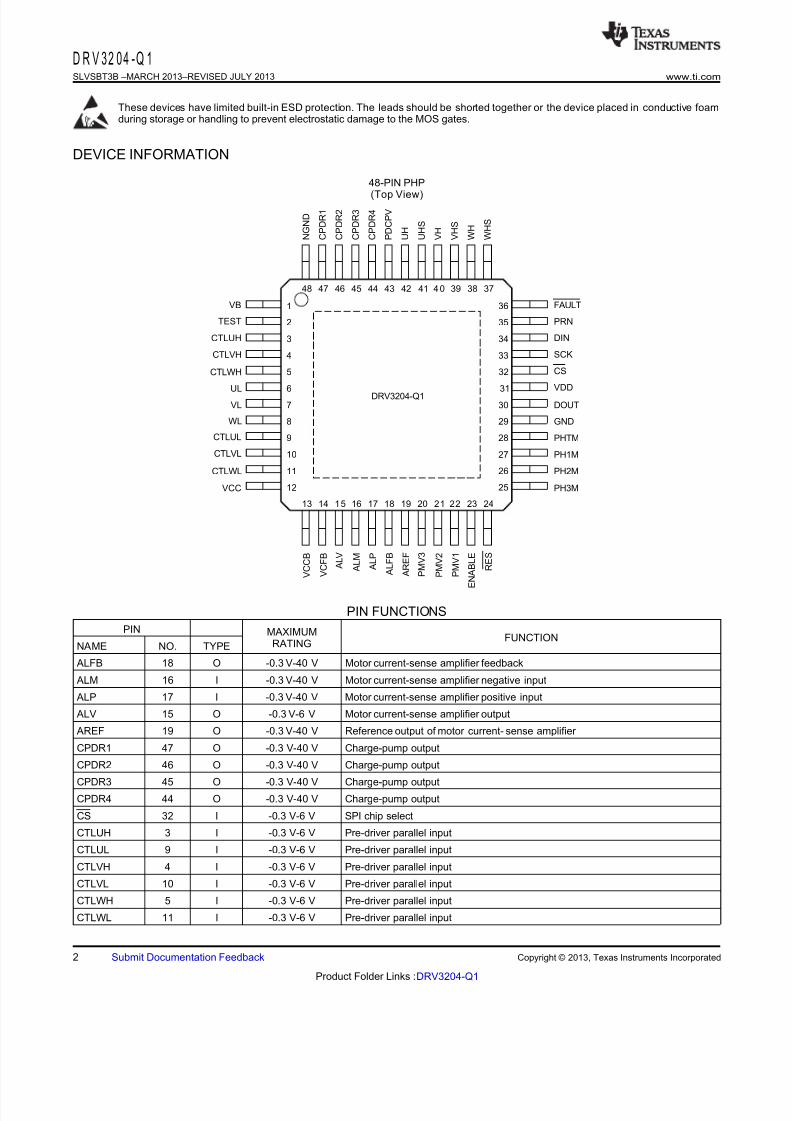
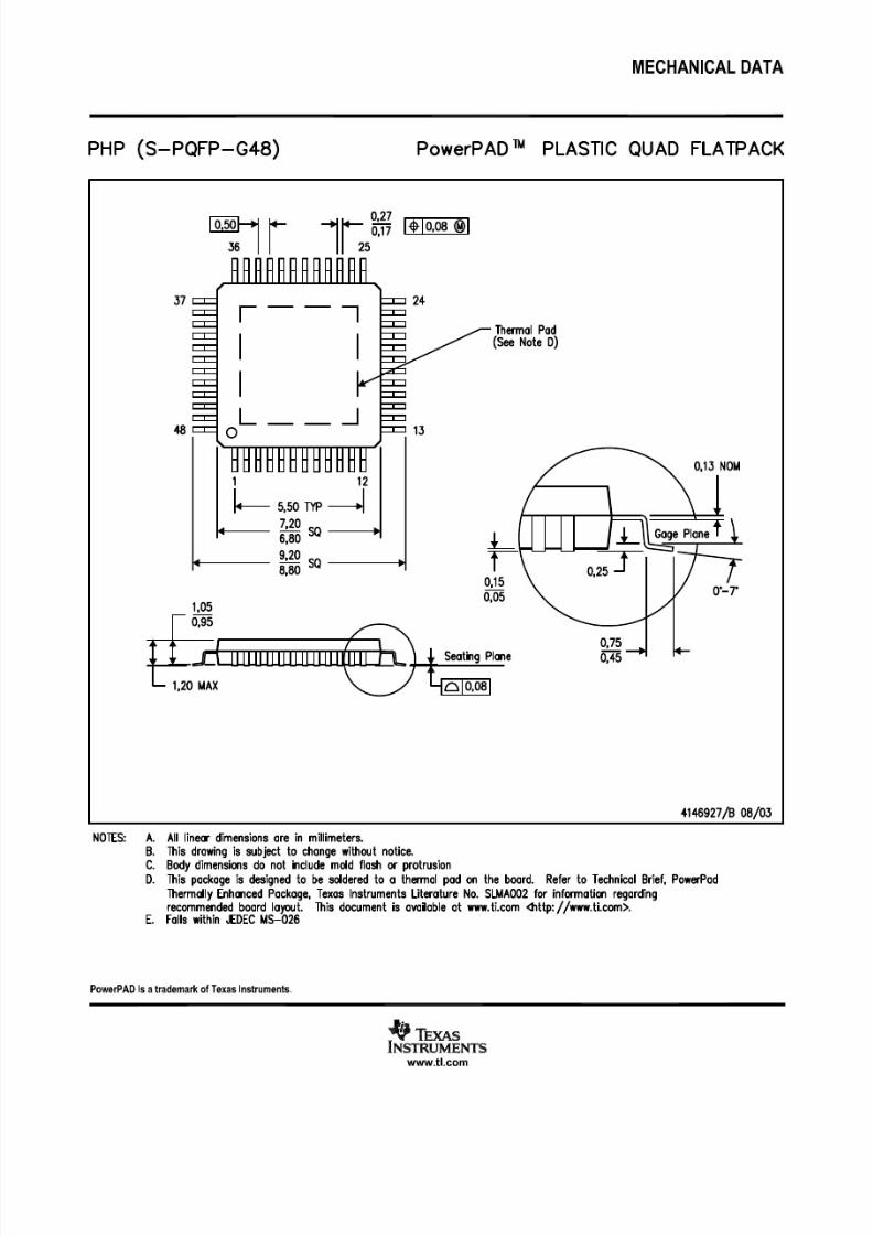
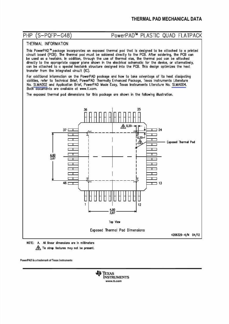
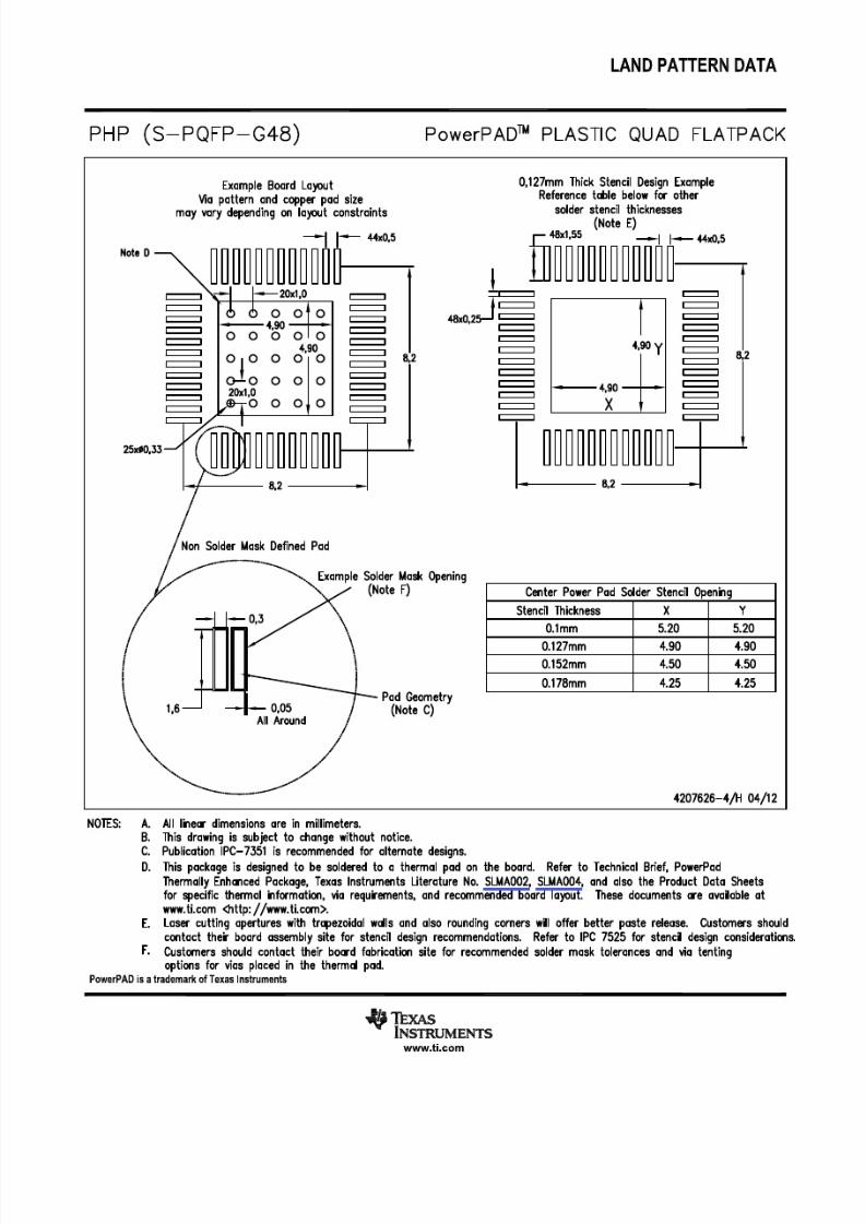
DEVICE INFORMATION
48-PIN PHP
(Top View)
PIN FUNCTIONS
PIN MAXIMUMFUNCTION
RATINGNAME NO. TYPE
ALFB 18 O -0.3 V-40 V Motor current-sense amplifier feedback
ALM 16 I -0.3 V-40 V Motor current-sense amplifier negative input
ALP 17 I -0.3 V-40 V Motor current-sense amplifier positive input
ALV 15 O -0.3 V-6 V Motor current-sense amplifier output
AREF 19 O -0.3 V-40 V Reference output of motor current- sense amplifier
CPDR1 47 O -0.3 V-40 V Charge-pump output
CPDR2 46 O -0.3 V-40 V Charge-pump output
CPDR3 45 O -0.3 V-40 V Charge-pump outputCPDR4 44 O -0.3 V-40 V Charge-pump output
CS 32 I -0.3 V-6 V SPI chip select
CTLUH 3 I -0.3 V-6 V Pre-driver parallel input
CTLUL 9 I -0.3 V-6 V Pre-driver parallel input
CTLVH 4 I -0.3 V-6 V Pre-driver parallel input
CTLVL 10 I -0.3 V-6 V Pre-driver parallel input
CTLWH 5 I -0.3 V-6 V Pre-driver parallel input
CTLWL 11 I -0.3 V-6 V Pre-driver parallel input
2 Submit Documentation Feedback Copyright © 2013, Texas Instruments Incorporated
Product Folder Links :DRV3204-Q1
8/10/2019 Slvsbt3b Three-Phase Brushless Motor Driver
http://slidepdf.com/reader/full/slvsbt3b-three-phase-brushless-motor-driver 3/38
D R V 32 04 -Q 1www.ti.com SLVSBT3B – MARCH 2013– REVISED JULY 2013
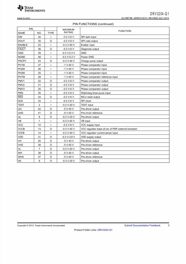
PIN FUNCTIONS (continued)
PIN MAXIMUMFUNCTION
RATINGNAME NO. TYPE
DIN 34 I -0.3 V-6 V SPI data input
DOUT 30 O -0.3 V-6 V SPI data output
ENABLE 23 I -0.3 V-40 V Enable inputFAULT 36 O -0.3 V-6 V Diagnosis output
GND 29 I -0.3 V-0.3 V GND
NGND 48 I -0.3 V-0.3 V Power GND
PDCPV 43 O -0.3 V-40 V Charge pump output
PH1M 27 I -1 V-40 V Phase comparator input
PH2M 26 I -1 V-40 V Phase comparator input
PH3M 25 I -1 V-40 V Phase comparator input
PHTM 28 I -1 V-40 V Phase comparator reference input
PMV1 22 O -0.3 V-6 V Phase comparator output
PMV2 21 O -0.3 V-6 V Phase comparator output
PMV3 20 O -0.3 V-6 V Phase comparator output
PRN 35 I -0.3 V-6 V Watchdog timer-pulse input
RES 24 O -0.3 V-6 V MCU reset output
SCK 33 I -0.3 V-6 V SPI clock
TEST 2 I -0.3 V-20 V TEST input
UH 42 O -5 V-40 V Pre-driver output
UHS 41 O -5 V-40 V Pre-driver reference
UL 6 O -0.3 V-20 V Pre-driver output
VB 1 I -0.3 V-40 V VB input
VCC 12 I -0.3 V-6 V VCC supply input
VCCB 13 O -0.3 V-40 V VCC regulator base driver of PNP external transistor
VCFB 14 I -0.3 V-40 V VCC regulator current-sense input
VDD 31 O -0.3 V-3.6 V VDD supply output
VH 40 O -5 V-40 V Pre-driver output
VHS 39 O -5 V-40 V Pre-driver reference
VL 7 O -0.3 V-20 V Pre-driver output
WH 38 O -5 V-40 V Pre-driver output
WHS 37 O -5 V-40 V Pre-driver reference
WL 8 O -0.3 V-20 V Pre-driver output
Copyright © 2013, Texas Instruments Incorporated Submit Documentation Feedback 3
Product Folder Links :DRV3204-Q1
8/10/2019 Slvsbt3b Three-Phase Brushless Motor Driver
http://slidepdf.com/reader/full/slvsbt3b-three-phase-brushless-motor-driver 4/38
48
OSC
47 46 45 44 43 42 41 40 39 38 37
36
35
34
33
32
31
30
29
28
27
26
25
1
2
3
4
5
6
7
8
9
10
11
12
13 14 15 16 17 18 19 20 21 22 23 24
Charge Pump
SCK
CS
DOUT
GND
PHTM
VDD
VCC
P MV 2
P MV 3
PH1M
N G N D
P D C P V
C P R D 1
C P R D 2
C P R D 3
C P R D 4
U H
VBMonitor
Control Logic
PH2M
VB
UL
VL
WL
R E S
V C C
P MV 1
V B
V M
V MS
AMP
VB
5V Reg
3.3V Reg
OV A D
A L V
A R E F
A L F B
A L M
A L P
TEST
(OPEN)
TEST I/F
AMP
- +COMP
A D T H
E N A B L E
V C C
U H S
V H
V H S
W H
W H S
P D C P V
P D C P V
P D C P V FAULT
PRN
DIN
PH3MWHS
VHS
UHS
VCOM
+-+-+-
C O M P
C O M P
C O M P
V C F B
V C C B
VCCB
VCFB
VCC
CTLWL
CTLVL
CTLUL
CTLWH
CTLVH
CTLUH
NGND
VCP12
VCP12TSD
SLEEP
WDVCC
VM
VB
UHS
VHS
WHS
Battery
M
UH
VH
WH
UL
VL
WL
VMS
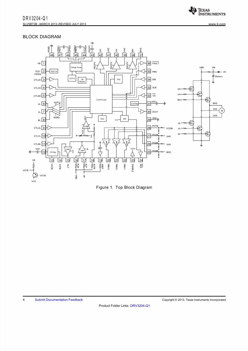
D R V 32 04 -Q 1SLVSBT3B –MARCH 2013–REVISED JULY 2013 www.ti.com
BLOCK DIAGRAM
Figure 1. Top Block Diagram
4 Submit Documentation Feedback Copyright © 2013, Texas Instruments Incorporated
Product Folder Links :DRV3204-Q1
8/10/2019 Slvsbt3b Three-Phase Brushless Motor Driver
http://slidepdf.com/reader/full/slvsbt3b-three-phase-brushless-motor-driver 5/38
D R V 32 04 -Q 1www.ti.com SLVSBT3B – MARCH 2013– REVISED JULY 2013
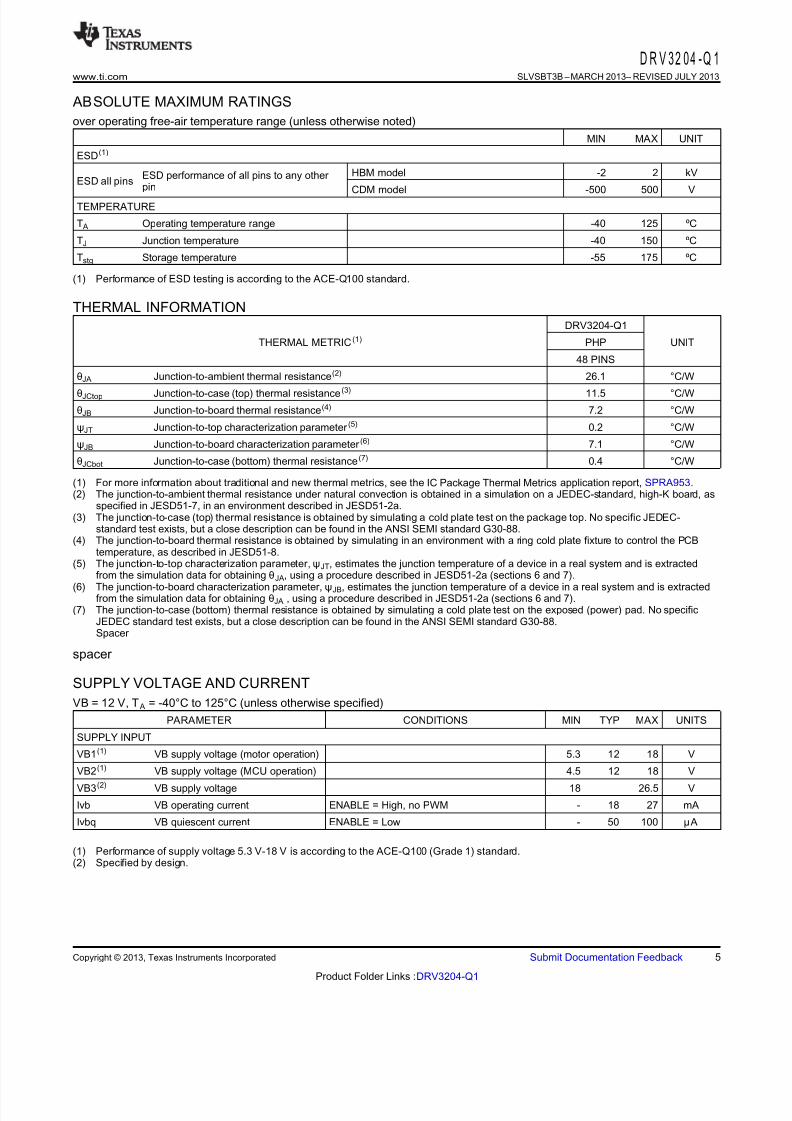
ABSOLUTE MAXIMUM RATINGS
over operating free-air temperature range (unless otherwise noted)
MIN MAX UNIT
ESD(1)
HBM model -2 2 kVESD performance of all pins to any other ESD all pins
pin CDM model -500 500 V
TEMPERATURE
T A Operating temperature range -40 125 ºC
TJ Junction temperature -40 150 ºC
Tstg Storage temperature -55 175 ºC
(1) Performance of ESD testing is according to the ACE-Q100 standard.
THERMAL INFORMATIONDRV3204-Q1
THERMAL METRIC (1) PHP UNIT
48 PINS
θJA Junction-to-ambient thermal resistance(2) 26.1 °C/W
θJCtop Junction-to-case (top) thermal resistance(3) 11.5 °C/W
θJB Junction-to-board thermal resistance(4) 7.2 °C/W
ψJT Junction-to-top characterization parameter (5) 0.2 °C/W
ψJB Junction-to-board characterization parameter (6) 7.1 °C/W
θJCbot Junction-to-case (bottom) thermal resistance(7) 0.4 °C/W
(1) For more information about traditional and new thermal metrics, see the IC Package Thermal Metrics application report, SPRA953.(2) The junction-to-ambient thermal resistance under natural convection is obtained in a simulation on a JEDEC-standard, high-K board, as
specified in JESD51-7, in an environment described in JESD51-2a.(3) The junction-to-case (top) thermal resistance is obtained by simulating a cold plate test on the package top. No specific JEDEC-
standard test exists, but a close description can be found in the ANSI SEMI standard G30-88.(4) The junction-to-board thermal resistance is obtained by simulating in an environment with a ring cold plate fixture to control the PCB
temperature, as described in JESD51-8.(5) The junction-to-top characterization parameter, ψJT, estimates the junction temperature of a device in a real system and is extracted
from the simulation data for obtaining θJA, using a procedure described in JESD51-2a (sections 6 and 7).
(6) The junction-to-board characterization parameter, ψJB, estimates the junction temperature of a device in a real system and is extractedfrom the simulation data for obtaining θJA , using a procedure described in JESD51-2a (sections 6 and 7).
(7) The junction-to-case (bottom) thermal resistance is obtained by simulating a cold plate test on the exposed (power) pad. No specificJEDEC standard test exists, but a close description can be found in the ANSI SEMI standard G30-88.Spacer
spacer
SUPPLY VOLTAGE AND CURRENT
VB = 12 V, T A = -40°C to 125°C (unless otherwise specified)
PARAMETER CONDITIONS MIN TYP MAX UNITS
SUPPLY INPUT
VB1(1) VB supply voltage (motor operation) 5.3 12 18 V
VB2(1) VB supply voltage (MCU operation) 4.5 12 18 V
VB3(2) VB supply voltage 18 26.5 V
Ivb VB operating current ENABLE = High, no PWM - 18 27 mA
Ivbq VB quiescent current ENABLE = Low - 50 100 µ A
(1) Performance of supply voltage 5.3 V-18 V is according to the ACE-Q100 (Grade 1) standard.(2) Specified by design.
Copyright © 2013, Texas Instruments Incorporated Submit Documentation Feedback 5
Product Folder Links :DRV3204-Q1
8/10/2019 Slvsbt3b Three-Phase Brushless Motor Driver
http://slidepdf.com/reader/full/slvsbt3b-three-phase-brushless-motor-driver 6/38
ClockMonitor
Watch Dog TimerWDT
Digital PatternDetection
Reset
Logic
PRN
RES
VCC
VDD
OSC1
3k
VCC
WDTEnable
Max 100pF
To MCU
100k
VCC
From MCU
VCC Under VoltageDetection
VDD Under VoltageDetection
D R V 32 04 -Q 1SLVSBT3B –MARCH 2013–REVISED JULY 2013 www.ti.com
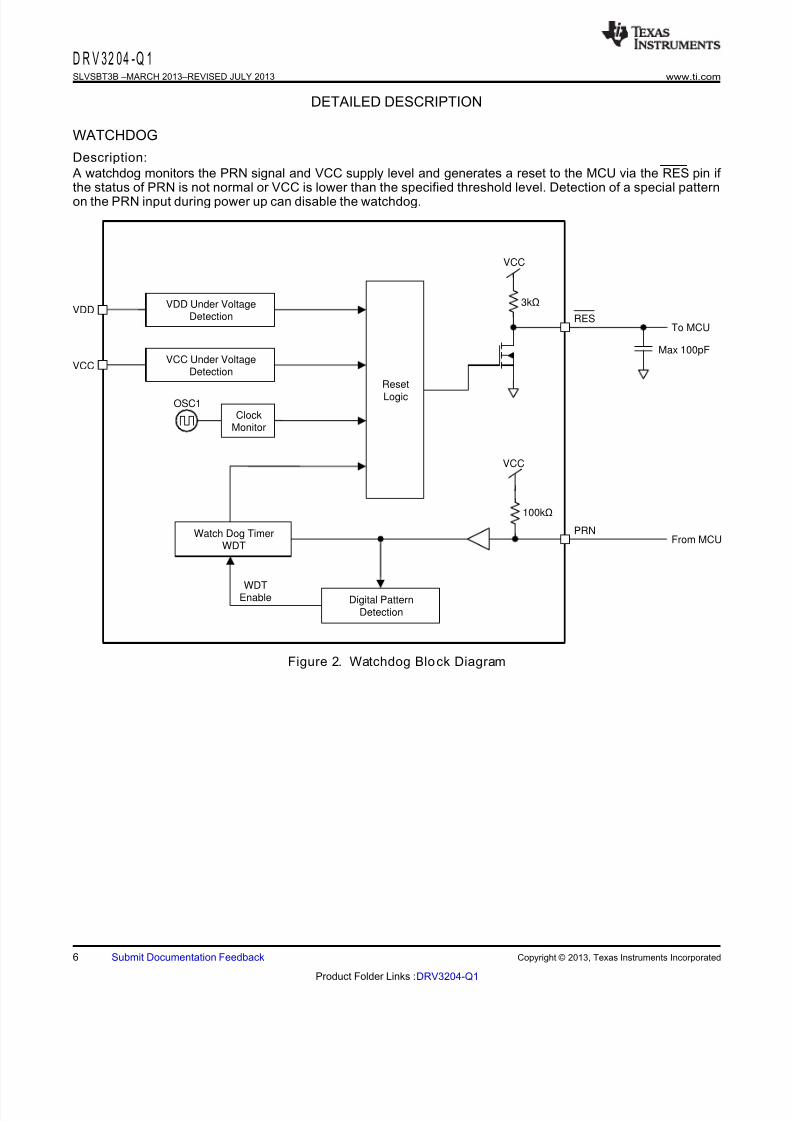
DETAILED DESCRIPTION
WATCHDOG
Description:
A watchdog monitors the PRN signal and VCC supply level and generates a reset to the MCU via the RES pin if the status of PRN is not normal or VCC is lower than the specified threshold level. Detection of a special patternon the PRN input during power up can disable the watchdog.
Figure 2. Watchdog Blo ck Diagram
6 Submit Documentation Feedback Copyright © 2013, Texas Instruments Incorporated
Product Folder Links :DRV3204-Q1
8/10/2019 Slvsbt3b Three-Phase Brushless Motor Driver
http://slidepdf.com/reader/full/slvsbt3b-three-phase-brushless-motor-driver 7/38
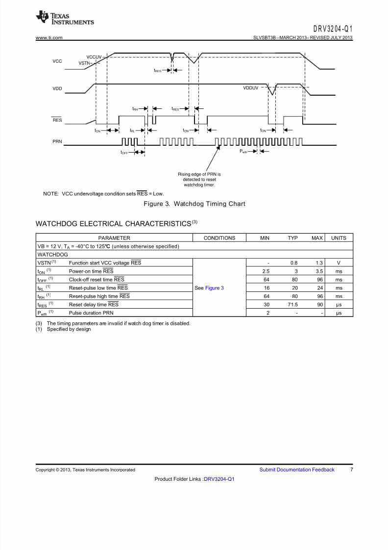
VCCVCCUV
RES
PRN
tRES
VSTN
VDDUVVDD
tRH tRES
tON tRL
Rising edge of PRN isdetected to resetwatchdog timer.
tOFF
tON tON
Pwth
D R V 32 04 -Q 1www.ti.com SLVSBT3B – MARCH 2013– REVISED JULY 2013
NOTE: VCC undervoltage condition sets RES = Low.
Figure 3. Watchdog Timing Chart
WATCHDOG ELECTRICAL CHARACTERISTICS (3)
PARAMETER CONDITIONS MIN TYP MAX UNITS
VB = 12 V, T A = -40°C to 125℃℃ (unless otherwise specified)
WATCHDOG
VSTN (1) Function start VCC voltage RES - 0.8 1.3 V
tON(1) Power-on time RES 2.5 3 3.5 ms
tOFF(1) Clock-off reset time RES 64 80 96 ms
tRL(1)
Reset-pulse low time RES See Figure 3 16 20 24 mstRH
(1) Reset-pulse high time RES 64 80 96 ms
tRES(1) Reset delay time RES 30 71.5 90 µs
Pwth(1) Pulse duration PRN 2 - - µs
(3) The timing parameters are invalid if watch dog timer is disabled.(1) Specified by design
Copyright © 2013, Texas Instruments Incorporated Submit Documentation Feedback 7
Product Folder Links :DRV3204-Q1
8/10/2019 Slvsbt3b Three-Phase Brushless Motor Driver
http://slidepdf.com/reader/full/slvsbt3b-three-phase-brushless-motor-driver 8/38
CS
DIN
SCK
SPI Control Logic and
8-Bit Shift Register 8-Bit Shift Register
Register Map
DOUT
System Clock
Enable
Address Write Data Read Data
Status
D R V 32 04 -Q 1SLVSBT3B –MARCH 2013–REVISED JULY 2013 www.ti.com
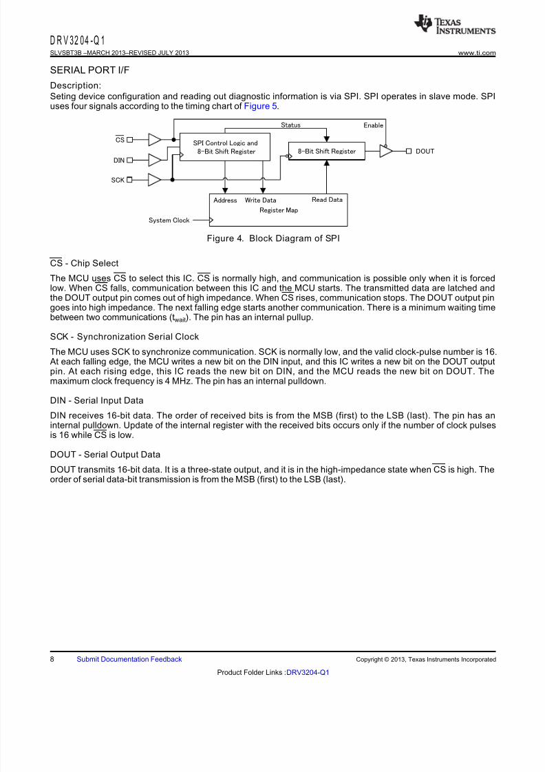
SERIAL PORT I/F
Description:
Seting device configuration and reading out diagnostic information is via SPI. SPI operates in slave mode. SPIuses four signals according to the timing chart of Figure 5.
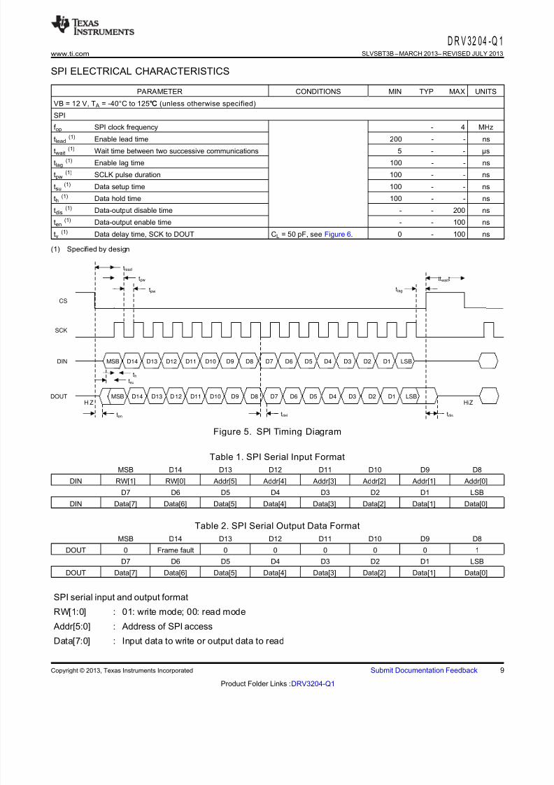
Figure 4. Block Diagram of SPI
CS - Chip Select
The MCU uses CS to select this IC. CS is normally high, and communication is possible only when it is forcedlow. When CS falls, communication between this IC and the MCU starts. The transmitted data are latched andthe DOUT output pin comes out of high impedance. When CS rises, communication stops. The DOUT output pingoes into high impedance. The next falling edge starts another communication. There is a minimum waiting timebetween two communications (twait). The pin has an internal pullup.
SCK - Synchronization Serial Clock
The MCU uses SCK to synchronize communication. SCK is normally low, and the valid clock-pulse number is 16. At each falling edge, the MCU writes a new bit on the DIN input, and this IC writes a new bit on the DOUT outputpin. At each rising edge, this IC reads the new bit on DIN, and the MCU reads the new bit on DOUT. Themaximum clock frequency is 4 MHz. The pin has an internal pulldown.
DIN - Serial Input Data
DIN receives 16-bit data. The order of received bits is from the MSB (first) to the LSB (last). The pin has aninternal pulldown. Update of the internal register with the received bits occurs only if the number of clock pulsesis 16 while CS is low.
DOUT - Serial Output Data
DOUT transmits 16-bit data. It is a three-state output, and it is in the high-impedance state when CS is high. Theorder of serial data-bit transmission is from the MSB (first) to the LSB (last).
8 Submit Documentation Feedback Copyright © 2013, Texas Instruments Incorporated
Product Folder Links :DRV3204-Q1
8/10/2019 Slvsbt3b Three-Phase Brushless Motor Driver
http://slidepdf.com/reader/full/slvsbt3b-three-phase-brushless-motor-driver 9/38
SCK
MSB D14 D13 D12 D11 D10 D9 D8 D7 D6 D5 D4 D3 D2 D1 LSBDIN
DOUT
CS
HiZ HiZMSB D14 D13 D 12 D11 D10 D9 D8 D7 D6 D5 D4 D3 D2 D1 LSB
tlead
tpw
tpw
tsu
th
ten tdel tdis
tlag
ttwaitt
D R V 32 04 -Q 1www.ti.com SLVSBT3B – MARCH 2013– REVISED JULY 2013
SPI ELECTRICAL CHARACTERISTICS
PARAMETER CONDITIONS MIN TYP MAX UNITS
VB = 12 V, T A = -40°C to 125℃℃ (unless otherwise specified)
SPI
f op SPI clock frequency - 4 MHz
tlead (1) Enable lead time 200 - - ns
twait(1) Wait time between two successive communications 5 - - µs
tlag(1) Enable lag time 100 - - ns
tpw(1) SCLK pulse duration 100 - - ns
tsu(1) Data setup time 100 - - ns
th(1) Data hold time 100 - - ns
tdis(1) Data-output disable time - - 200 ns
ten(1) Data-output enable time - - 100 ns
tv(1) Data delay time, SCK to DOUT CL = 50 pF, see Figure 6. 0 - 100 ns
(1) Specified by design
Figure 5. SPI Timing Diagram
Table 1. SPI Serial Input Format
MSB D14 D13 D12 D11 D10 D9 D8
DIN RW[1] RW[0] Addr[5] Addr[4] Addr[3] Addr[2] Addr[1] Addr[0]
D7 D6 D5 D4 D3 D2 D1 LSB
DIN Data[7] Data[6] Data[5] Data[4] Data[3] Data[2] Data[1] Data[0]
Table 2. SPI Serial Output Data Format
MSB D14 D13 D12 D11 D10 D9 D8
DOUT 0 Frame fault 0 0 0 0 0 1D7 D6 D5 D4 D3 D2 D1 LSB
DOUT Data[7] Data[6] Data[5] Data[4] Data[3] Data[2] Data[1] Data[0]
SPI serial input and output format
RW[1:0] : 01: write mode; 00: read mode
Addr[5:0] : Address of SPI access
Data[7:0] : Input data to write or output data to read
Copyright © 2013, Texas Instruments Incorporated Submit Documentation Feedback 9
Product Folder Links :DRV3204-Q1
8/10/2019 Slvsbt3b Three-Phase Brushless Motor Driver
http://slidepdf.com/reader/full/slvsbt3b-three-phase-brushless-motor-driver 10/38
D R V 32 04 -Q 1SLVSBT3B –MARCH 2013–REVISED JULY 2013 www.ti.com
Frame fault : 0: No error exists in the previous SPI frame.
: 1: Error exists in the previous SPI frame.
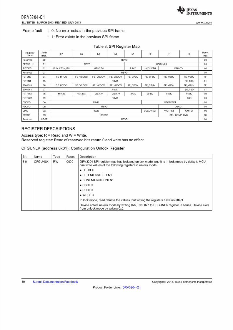
Table 3. SPI Register Map
Add r ResetRegister b7 b6 b5 b4 b3 b2 b1 b0
Name (Hex) (Hex)
Reserved 00 RSVD 00
CFGUNLK 01 RSVD CFGUNLK 00
FLTCFG 02 FLGLATCH_EN MTOCTH RSVD VCCUVTH VBUVTH 00
Reserved 03 RSVD 00
FLTEN0 04 FE_MTOC FE_VCCOC FE_VCCOV F E_VDDOV FE_CPOV FE_CPUV FE_VBOV FE_VBUV FF
FLTEN1 05 RSVD FE_TSD 01
SDNEN0 06 SE_MTOC SE_VCCOC SE_VCCOV SE_VDDOV SE_CPOV SE_CPUV SE_VBOV SE_VBUV FF
SDNEN1 07 RSVD SE_TSD 01
FLTFLG0 08 MTOC VCCOC VCCOV VDDOV CPOV CPUV VBOV VBUV 00
FLTFLG1 09 RSVD TSD 00
CSCFG 0A RSVD CSOFFSET 00
PDCFG 0B RSVD DEADT 00
DIAG 0C RSVD VCCUVRST WDTRST CMRST 00
SPARE 0D SPARE SEL_COMP_HYS 00
Reserved 0E-3F RSVD 00
REGISTER DESCRIPTIONS
Access type: R = Read and W = Write.
Reserved register: Read of reserved bits return 0 and write has no effect.
CFGUNLK (address 0x01): Configuration Unlock Register
Bit Name Type Reset Description
3:0 CFGUNLK RW 0000 DRV3204 SPI register map has lock and unlock mode, and it is in lock mode by default. MCUcan write values of the following registers in unlock mode;
● FLTCFG
● FLTEN0 and FLTEN1
● SDNEN0 and SDNEN1
● CSCFG
● PDCFG
● WDCFG
In lock mode, read returns the values, but writing the registers have no effect.
Device enters unlock mode by writing 0x5, 0x8, 0x7 to CFGUNLK register in series. Device exitsfrom unlock mode by writing 0x0.
10 Submit Documentation Feedback Copyright © 2013, Texas Instruments Incorporated
Product Folder Links :DRV3204-Q1
8/10/2019 Slvsbt3b Three-Phase Brushless Motor Driver
http://slidepdf.com/reader/full/slvsbt3b-three-phase-brushless-motor-driver 11/38
D R V 32 04 -Q 1www.ti.com SLVSBT3B – MARCH 2013– REVISED JULY 2013
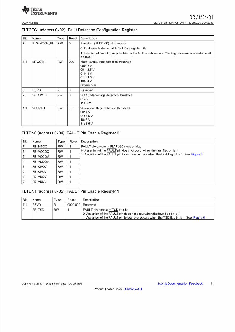
FLTCFG (address 0x02): Fault Detection Configuration Register
Bit Name Type Reset Description
7 FLGLATCH_EN RW 0 Fault-f lag (FLTFLG*) latch enable
0: Fault events do not latch fault-flag register bits.
1: Latching of fault-flag register bits by the fault events occurs. The flag bits remain asserted until
cleared.6:4 MTOCTH RW 000 Motor overcurrent detection threshold
000: 2 V
001: 2.5 V
010: 3 V
011: 3.5 V
100: 4 V
Others: 2 V
3 RSVD R 0 Reserved
2 VCCUVTH RW 0 VCC undervoltage detection threshold
0: 4 V
1: 4.2 V
1:0 VBUVTH RW 00 VB undervoltage detection threshold
00: 4 V
01: 4.5 V10: 5 V
11: 5.5 V
FLTEN0 (address 0x04): FAULT Pin Enable Register 0
Bit Name Type Reset Description
7 FE_MTOC RW 1 FAULT pin enable of FLTFLG0 register bits.
0: Assertion of the FAULT pin does not occur when the fault flag bit is 16 FE_VCCOC RW 11: Assertion of the FAULT pin to low level occurs when the fault flag bit is 1. See Figure 6
5 FE_VCCOV RW 1
4 FE_VDDOV RW 1
3 FE_CPOV RW 1
2 FE_CPUV RW 1
1 FE_VBOV RW 1
0 FE_VBUV RW 1
FLTEN1 (address 0x05): FAULT Pin Enable Register 1
Bit Name Type Reset Description
7:1 RSVD R 0000 000 Reserved
0 FE_TSD RW 1 FAULT pin enable of TSD flag bit
0: Assertion of the FAULT pin does not occur when the fault flag bit is 1
1: Assertion of the FAULT pin to low level occurs when the TSD flag bit is 1. See Figure 6
Copyright © 2013, Texas Instruments Incorporated Submit Documentation Feedback 11
Product Folder Links :DRV3204-Q1
8/10/2019 Slvsbt3b Three-Phase Brushless Motor Driver
http://slidepdf.com/reader/full/slvsbt3b-three-phase-brushless-motor-driver 12/38
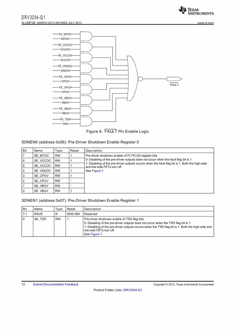
TSD
FE_TSD
VBUV
FE_VBUV
VBOV
FE_VBOV
CPUV
FE_CPUV
CPOV
FE_CPOV
VDDOV
FE_VDDOV
VCCOV
FE_VCCOV
VCCOC
FE_VCCOC
MTOC
FE_MTOC
FAULT
D R V 32 04 -Q 1SLVSBT3B –MARCH 2013–REVISED JULY 2013 www.ti.com
Figure 6. FAULT Pin Enable Logic
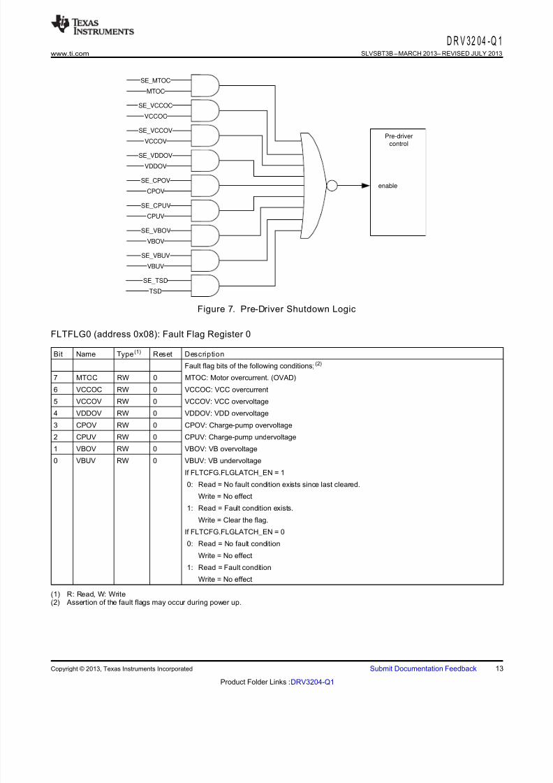
SDNEN0 (address 0x06): Pre-Driver Shutdown Enable Register 0
Bit Name Type Reset Description
7 SE_MTOC RW 1 Pre-driver shutdown enable of FLTFLG0 register bits
0: Disabling of the pre-driver outputs does not occur when the fault flag bit is 1.6 SE_VCCOC RW 11: Disabling of the pre-driver outputs occurs when the fault flag bit is 1. Both the high-side
5 SE_VCCOV RW 1 and low-side FETs turn off.
4 SE_VDDOV RW 1 See Figure 7.
3 SE_CPOV RW 1
2 SE_CPUV RW 1
1 SE_VBOV RW 1
0 SE_VBUV RW 1
SDNEN1 (address 0x07): Pre-Driver Shutdown Enable Register 1
Bit Name Type Reset Description
7:1 RSVD R 0000 000 Reserved
0 SE_TSD RW 1 Pre-driver shutdown enable of TSD flag bits
0: Disabling of the pre-driver outputs does not occur when the TSD flag bit is 1.
1: Disabling of the pre-driver outputs occurs when the TSD flag bit is 1. Both the high-side andlow-side FETs turn off.
See Figure 7.
12 Submit Documentation Feedback Copyright © 2013, Texas Instruments Incorporated
Product Folder Links :DRV3204-Q1
8/10/2019 Slvsbt3b Three-Phase Brushless Motor Driver
http://slidepdf.com/reader/full/slvsbt3b-three-phase-brushless-motor-driver 13/38
TSD
SE_TSD
VBUV
SE_VBUV
VBOV
SE_VBOV
CPUV
SE_CPUV
CPOV
SE_CPOV
VDDOV
SE_VDDOV
VCCOV
SE_VCCOV
VCCOC
SE_VCCOC
MTOC
SE_MTOC
Pre-drivercontrol
enable
D R V 32 04 -Q 1www.ti.com SLVSBT3B – MARCH 2013– REVISED JULY 2013
Figure 7. Pre-Driver Shutdown Logic
FLTFLG0 (address 0x08): Fault Flag Register 0
Bit Name Type (1) Reset Description
Fault flag bits of the following conditions; (2)
7 MTOC RW 0 MTOC: Motor overcurrent. (OVAD)
6 VCCOC RW 0 VCCOC: VCC overcurrent
5 VCCOV RW 0 VCCOV: VCC overvoltage
4 VDDOV RW 0 VDDOV: VDD overvoltage
3 CPOV RW 0 CPOV: Charge-pump overvoltage
2 CPUV RW 0 CPUV: Charge-pump undervoltage
1 VBOV RW 0 VBOV: VB overvoltage
0 VBUV RW 0 VBUV: VB undervoltage
If FLTCFG.FLGLATCH_EN = 1
0: Read = No fault condition exists since last cleared.
Write = No effect
1: Read = Fault condition exists.
Write = Clear the flag.
If FLTCFG.FLGLATCH_EN = 0
0: Read = No fault condition
Write = No effect
1: Read = Fault condition
Write = No effect
(1) R: Read, W: Write(2) Assertion of the fault flags may occur during power up.
Copyright © 2013, Texas Instruments Incorporated Submit Documentation Feedback 13
Product Folder Links :DRV3204-Q1
8/10/2019 Slvsbt3b Three-Phase Brushless Motor Driver
http://slidepdf.com/reader/full/slvsbt3b-three-phase-brushless-motor-driver 14/38
FLTFLG*Status N
FLTFLG*Status N+1
CS
SCK
Fault Event Status N Status N+1
SPI Read Buffer Status N Status N+1
SPI DOUT
Serial Output Format Serial Output Format
D R V 32 04 -Q 1SLVSBT3B –MARCH 2013–REVISED JULY 2013 www.ti.com
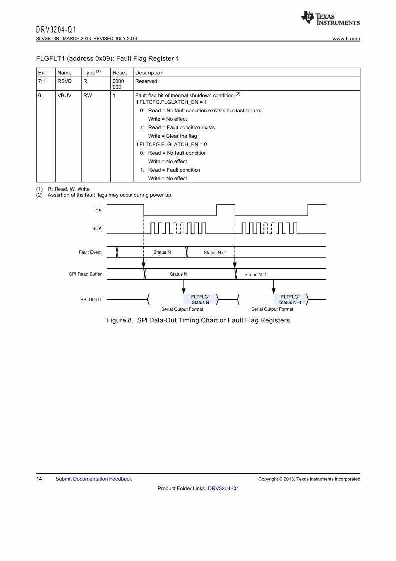
FLGFLT1 (address 0x09): Fault Flag Register 1
Bit Name Type (1) Reset Descript ion
7:1 RSVD R 0000 Reserved000
0 VBUV RW 1 Fault flag bit of thermal shutdown condition.(2)
If FLTCFG.FLGLATCH_EN = 1
0: Read = No fault condition exists since last cleared.
Write = No effect
1: Read = Fault condition exists.
Write = Clear the flag
If FLTCFG.FLGLATCH_EN = 0
0: Read = No fault condition
Write = No effect
1: Read = Fault condition
Write = No effect
(1) R: Read, W: Write
(2) Assertion of the fault flags may occur during power up.
Figure 8. SPI Data-Out Timing Chart o f Fault Flag Registers
14 Submit Documentation Feedback Copyright © 2013, Texas Instruments Incorporated
Product Folder Links :DRV3204-Q1
8/10/2019 Slvsbt3b Three-Phase Brushless Motor Driver
http://slidepdf.com/reader/full/slvsbt3b-three-phase-brushless-motor-driver 15/38
Status
FLGLATCH_EN 0 1
Fault Fault
10
Read Write 1to cClear
FLTFLG
SPI Accessto FLTFLG
FAULT(1)
LH
DisableEnablePre-Driver(2)
D R V 32 04 -Q 1www.ti.com SLVSBT3B – MARCH 2013– REVISED JULY 2013
(1) Assertion of FAULT occurs if FLTEN = 1.
(2) Disabling of pre-driveroccurs if SDNEN = 1.
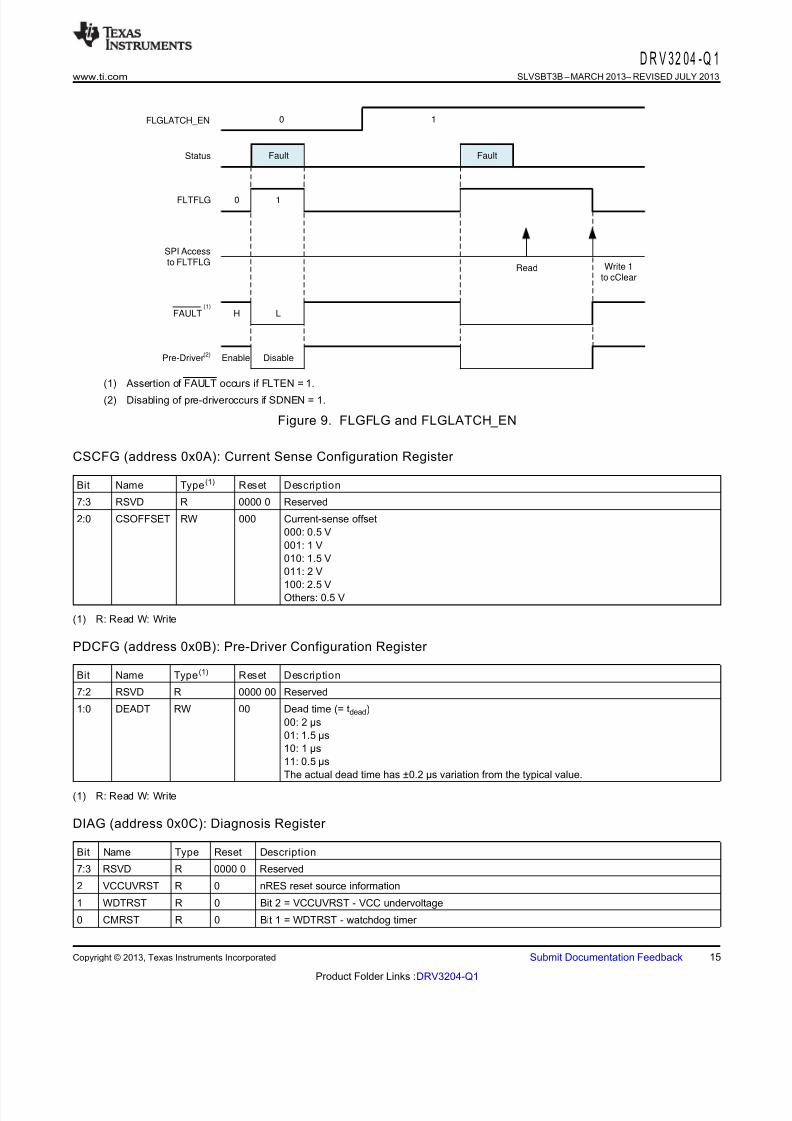
Figure 9. FLGFLG and FLGLATCH_EN
CSCFG (address 0x0A): Current Sense Configuration Register
Bit Name Type (1) Reset Description
7:3 RSVD R 0000 0 Reserved
2:0 CSOFFSET RW 000 Current-sense offset
000: 0.5 V
001: 1 V
010: 1.5 V
011: 2 V
100: 2.5 VOthers: 0.5 V
(1) R: Read W: Write
PDCFG (address 0x0B): Pre-Driver Configuration Register
Bit Name Type (1) Reset Description
7:2 RSVD R 0000 00 Reserved
1:0 DEADT RW 00 Dead time (= tdead)
00: 2 µs
01: 1.5 µs
10: 1 µs
11: 0.5 µs
The actual dead time has ±0.2 µs variation from the typical value.
(1) R: Read W: Write
DIAG (address 0x0C): Diagnosis Register
Bit Name Type Reset Description
7:3 RSVD R 0000 0 Reserved
2 VCCUVRST R 0 nRES reset source information
1 WDTRST R 0 Bit 2 = VCCUVRST - VCC undervoltage
0 CMRST R 0 Bit 1 = WDTRST - watchdog timer
Copyright © 2013, Texas Instruments Incorporated Submit Documentation Feedback 15
Product Folder Links :DRV3204-Q1
8/10/2019 Slvsbt3b Three-Phase Brushless Motor Driver
http://slidepdf.com/reader/full/slvsbt3b-three-phase-brushless-motor-driver 16/38
D R V 32 04 -Q 1SLVSBT3B –MARCH 2013–REVISED JULY 2013 www.ti.com
Bit Name Type Reset Description
Bit 0 = CMRST - clock monitor
0: Read = Reset has not occurred.
Write = No effect
1: Read = A corresponding reset source caused the last reset condition.
Write = No effect
Read access to this register clears the bits.
SPARE (address 0x0D): Spare Register
Bit Name Type (1) Reset Description
7:2 SPARE RW 0000 Spare registers for future use. Read and write have no effect.00
1:0 SEL_COMP_HY RW 00 Select phase comparator hysteresis voltage. The following show the typical values.S MM 00: 0 V
MM 01: 25 mV
MM 10: 50 mV
MM 11: 100 mV
(1) R: Read W: Write
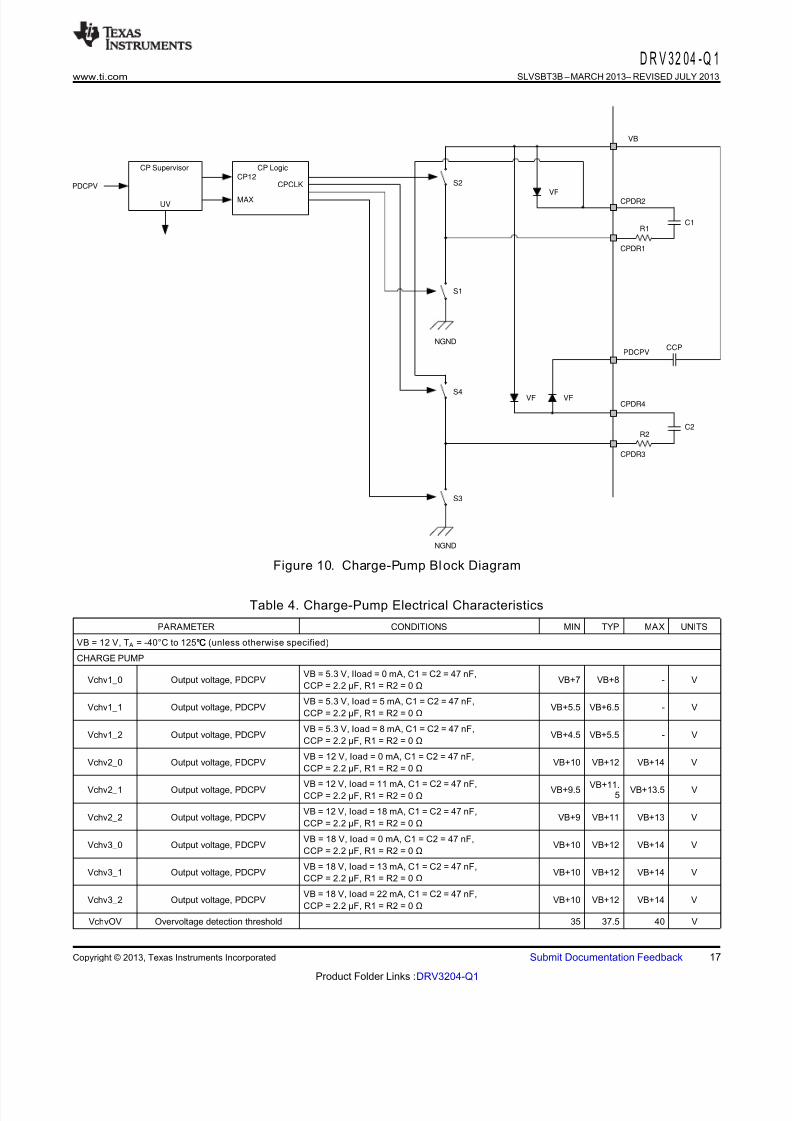
CHARGE PUMP
Description:
The charge-pump block generates a supply for the high-side and low-side pre-drivers to maintain the gatevoltage on the external FETs. Use of an external storage capacitor (CCP) and bucket capacitors (C1, C2)supports pre-driver slope and switching-frequency requirements. R1 and R2 can reduce switching current if required. The charge pump has voltage-supervisor functions such as over- and undervoltage, and selectablestop conditions for pre-drivers.
16 Submit Documentation Feedback Copyright © 2013, Texas Instruments Incorporated
Product Folder Links :DRV3204-Q1
8/10/2019 Slvsbt3b Three-Phase Brushless Motor Driver
http://slidepdf.com/reader/full/slvsbt3b-three-phase-brushless-motor-driver 17/38
VF
VB
C1
CCP
VF VF
PDCPV
CPDR4
CPDR3
C2
CP Logic
CPDR1
CPDR2
S1
S2
S4
S3
NGND
NGND
CP12
MAX
CP Supervisor
PDCPV
UV
CPCLK
R2
R1
D R V 32 04 -Q 1www.ti.com SLVSBT3B – MARCH 2013– REVISED JULY 2013
Figure 10. Charge-Pump Bl ock Diagram
Table 4. Charge-Pump Electrical Characteristics
PARAMETER CONDITIONS MIN TYP MAX UNITS
VB = 12 V, T A = -40°C to 125℃℃ (unless otherwise specified)
CHARGE PUMP
VB = 5.3 V, Iload = 0 mA, C1 = C2 = 47 nF,Vchv1_0 Output voltage, PDCPV VB+7 VB+8 - V
CCP = 2.2 µF, R1 = R2 = 0 Ω
VB = 5.3 V, Ioad = 5 mA, C1 = C2 = 47 nF,Vchv1_1 Output voltage, PDCPV VB+5.5 VB+6.5 - V
CCP = 2.2 µF, R1 = R2 = 0 Ω
VB = 5.3 V, Ioad = 8 mA, C1 = C2 = 47 nF,Vchv1_2 Output voltage, PDCPV VB+4.5 VB+5.5 - V
CCP = 2.2 µF, R1 = R2 = 0 Ω
VB = 12 V, Ioad = 0 mA, C1 = C2 = 47 nF,Vchv2_0 Output voltage, PDCPV VB+10 VB+12 VB+14 V
CCP = 2.2 µF, R1 = R2 = 0 Ω
VB = 12 V, Ioad = 11 mA, C1 = C2 = 47 nF, VB+11.Vchv2_1 Output voltage, PDCPV VB+9.5 VB+13.5 V5CCP = 2.2 µF, R1 = R2 = 0 Ω
VB = 12 V, Ioad = 18 mA, C1 = C2 = 47 nF,Vchv2_2 Output voltage, PDCPV VB+9 VB+11 VB+13 V
CCP = 2.2 µF, R1 = R2 = 0 Ω
VB = 18 V, Ioad = 0 mA, C1 = C2 = 47 nF,Vchv3_0 Output voltage, PDCPV VB+10 VB+12 VB+14 V
CCP = 2.2 µF, R1 = R2 = 0 Ω
VB = 18 V, Ioad = 13 mA, C1 = C2 = 47 nF,Vchv3_1 Output voltage, PDCPV VB+10 VB+12 VB+14 V
CCP = 2.2 µF, R1 = R2 = 0 Ω
VB = 18 V, Ioad = 22 mA, C1 = C2 = 47 nF,Vchv3_2 Output voltage, PDCPV VB+10 VB+12 VB+14 V
CCP = 2.2 µF, R1 = R2 = 0 Ω
VchvOV Overvoltage detection threshold 35 37.5 40 V
Copyright © 2013, Texas Instruments Incorporated Submit Documentation Feedback 17
Product Folder Links :DRV3204-Q1
8/10/2019 Slvsbt3b Three-Phase Brushless Motor Driver
http://slidepdf.com/reader/full/slvsbt3b-three-phase-brushless-motor-driver 18/38
CTLxHH : PU onL : PD on
UHS/
VHS/ WHS
UH/VH/WH
High Side Pre Driver
UL/VL /WL
RL
RL
PD CTRL
PDCPV
CTLxLH : PU onL : PD on
NGND
Low Side Pre Driver
PD CTRL
CL
CL
PDCPV
LVS
VCP12
D R V 32 04 -Q 1SLVSBT3B –MARCH 2013–REVISED JULY 2013 www.ti.com
Table 4. Charge-Pump Electrical Characteristics (continued)
PARAMETER CONDITIONS MIN TYP MAX UNITS
VchvUV Undervoltage detection threshold VB+4 VB+4.5 VB+5 V
VB = 5.3 V, C1 = C2 = 47 nF, CCP = 2.2 µF,tchv
(1) Rise time 1 2 msR1 = R2 = 0 Ω, Vchv, UV released
Ron On-resistance, S1-S4 See Figure 10 8 Ω
(1) Specified by design
Pre-Driver
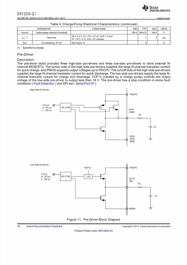
Description:
The pre-driver block provides three high-side pre-drivers and three low-side pre-drivers to drive external N-channel MOSFETs. The turnon side of the high-side pre-drivers supplies the large N-channel transistor currentfor quick charge, and PMOS supports output voltages up to PDCPV. The turnoff side of the high-side pre-driverssupplies the large N-channel transistor current for quick discharge. The low-side pre-drivers supply the large N-channel transistor current for charge and discharge. VCP12 (created by a charge pump) controls the outputvoltage of the low-side pre-driver to output less than 18 V. The pre-driver has a stop condition in some faultconditions ( Fault Detection ) and SPI set ( Serial Port I/F ).
Figure 11. Pre-Driver Block Diagram
18 Submit Documentation Feedback Copyright © 2013, Texas Instruments Incorporated
Product Folder Links :DRV3204-Q1
8/10/2019 Slvsbt3b Three-Phase Brushless Motor Driver
http://slidepdf.com/reader/full/slvsbt3b-three-phase-brushless-motor-driver 19/38
D R V 32 04 -Q 1www.ti.com SLVSBT3B – MARCH 2013– REVISED JULY 2013
Table 5. Pre-Driver Electrical Characteristics
PARAMETER CONDITIONS MIN TYP MAX UNITS
VB = 12 V unless otherwise stated, T A = -40ºC to 125℃℃, unless otherwise specified
HIGH-SIDE PRE-DRIVER
VOH_H Output voltage, turnon side Isink = 10 mA, PDCPV - xH 1.35 2.7 V
VOL_H Output voltage, turnoff side Isource = 10 mA, xH - xHS 25 50 mV
RONH_HP On-resistance, turnon side (Pch) U(V/W)H = PDCPV - 1 V 135 270 Ω
RONH_HN On-resistance, turnon side (Nch) U(V/W)H = PDCPV - 2.5 V 4 8 Ω
RONL_H On-resistance turnoff side 2.5 5 Ω
ton_h1(1) Turnon time CL = 12 nF, RL = 0 Ω from 20% to 80% 50 - 200 ns
toff_h1(1) Turnoff time CL = 12 nF, RL = 0 Ω from 80% to 20% 50 - 200 ns
th-ondly1(1) Output delay time CL = 12 nF, RL = 0 Ω to 20%, no dead time - 200 - ns
th-offdly1(1) Output delay time CL = 12 nF, RL = 0 Ω to 80%, no dead time - 200 - ns
Gate-source high -side voltageVGS_hs xH-xHS -0.3 18 V
difference
LOW-SIDE PRE-DRIVER
VOH_L1 Output voltage, turnon side VB = 12 V, Isink = 10 mA, xL -NGND 10 12 14 V
VOH_L2 Output voltage, turnon side VB = 5.3 V, Isink = 10 mA, xL - NGND 5.5 7.5 10 VVOL_L Output voltage, turnoff side Isource = 10 mA, xL - NGND - 25 50 mV
RONH_L On-resistance, turnon side - 6 12 Ω
RONL_L On-resistance, turnoff side 2.5 5 Ω
CL = 18 nF, RL = 0 Ω,ton_l
(1) Turnon time from 20% to 80% of 12 V, 50 - 200 nsfrom 20% to 80% of 6 V (VB = 5.3 V)
CL = 18 nF, RL = 0 Ω,toff_h
(1) Turnoff time from 80% to 20% of 12 V, 50 - 200 nsfrom 80% to 20% of 6 V (VB = 5.3 V)
CL = 18 nF, RL = 0 Ω,to 20% of 12 V,
tl-ondly(1) Output delay time - 200 - ns
to 20% of VOH = 6 V (VB = 5.3 V),no dead time
CL = 18 nF, RL = 0 Ω,to 80% of 12 V,
tl-offdly(1) Output delay time - 200 - ns
to 80% of VOH = 6 V (VB = 5.3 V),no dead time
(Th-on) - (Tl-off), no dead time,tdiff1
(1) Differential time1 -200 0 200 nsSee Figure 12
(Tl-on) - (Tl-off), no dead time,tdiff2
(1) Differential time2 -200 0 200 nsSee Figure 12
2 2.2
1.5 1.7tdead
(1) Dead time OSC1 = 10 MHz SPI register PDCFG.DEADT µs1 1.2
0.5 0.7
(1) Specified by design
Copyright © 2013, Texas Instruments Incorporated Submit Documentation Feedback 19
Product Folder Links :DRV3204-Q1
8/10/2019 Slvsbt3b Three-Phase Brushless Motor Driver
http://slidepdf.com/reader/full/slvsbt3b-three-phase-brushless-motor-driver 20/38
CTLULCTLVLCTLWL
UHVHWH
ULVLWL
CTLUHCTLVHCTLWH
th-offdlytdead + th-ondly
tl-offdly tdead + tl-ondly
th-off(th-offdly + toff)
CTLULCTLVLCTLWL
UHVH
WH
ULVLWL
xHS
80%
20%
80%
20%
80%
20%
80%
20% NGND
CTLUHCTLVHCTLWH
th-ondly th-offdly
th-on(th-ondly + ton)
tl-ondly
tl-on(tl-ondly + ton)
tl-offdly
tl-off(tl-offdly + toff)
D R V 32 04 -Q 1SLVSBT3B –MARCH 2013–REVISED JULY 2013 www.ti.com
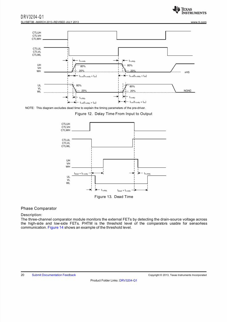
NOTE: This diagram excludes dead time to explain the timing parameters of the pre-driver.
Figure 12. Delay Time From Input to Output
Figure 13. Dead Time
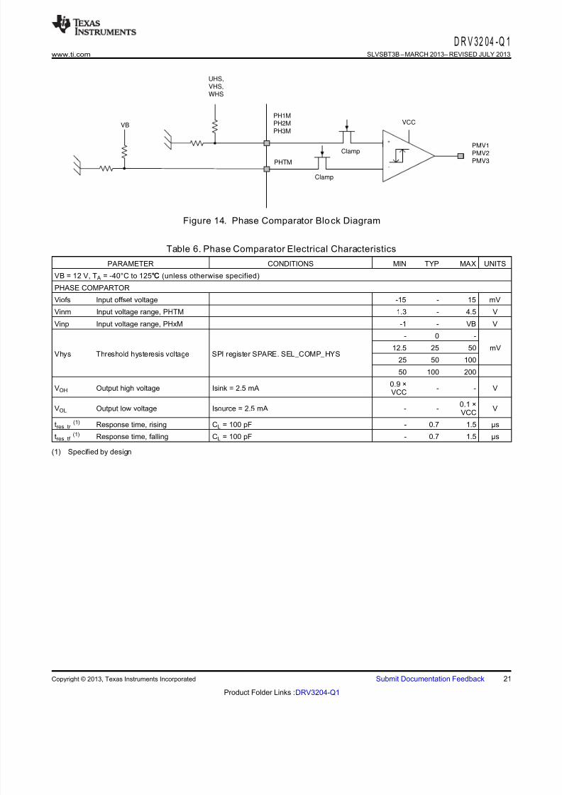
Phase Comparator
Description:
The three-channel comparator module monitors the external FETs by detecting the drain-source voltage acrossthe high-side and low-side FETs. PHTM is the threshold level of the comparators usable for sensorlesscommunication. Figure 14 shows an example of the threshold level.
20 Submit Documentation Feedback Copyright © 2013, Texas Instruments Incorporated
Product Folder Links :DRV3204-Q1
8/10/2019 Slvsbt3b Three-Phase Brushless Motor Driver
http://slidepdf.com/reader/full/slvsbt3b-three-phase-brushless-motor-driver 21/38
-
+PMV1PMV2PMV3PHTM
PH1MPH2MPH3M
UHS,VHS,WHS
VCC
Clamp
Clamp
VB
D R V 32 04 -Q 1www.ti.com SLVSBT3B – MARCH 2013– REVISED JULY 2013
Figure 14. Phase Comparator Blo ck Diagram
Table 6. Phase Comparator Electrical Characteristics
PARAMETER CONDITIONS MIN TYP MAX UNITS
VB = 12 V, T A = -40°C to 125℃℃
(unless otherwise specified)PHASE COMPARTOR
Viofs Input offset voltage -15 - 15 mV
Vinm Input voltage range, PHTM 1.3 - 4.5 V
Vinp Input voltage range, PHxM -1 - VB V
- 0 -
12.5 25 50 mVVhys Threshold hysteresis voltage SPI register SPARE. SEL_COMP_HYS
25 50 100
50 100 200
0.9 ×VOH Output high voltage Isink = 2.5 mA - - V
VCC
0.1 ×VOL Output low voltage Isource = 2.5 mA - - V
VCC
tres_tr (1) Response time, rising CL = 100 pF - 0.7 1.5 µs
tres_tf (1) Response time, falling CL = 100 pF - 0.7 1.5 µs
(1) Specified by design
Copyright © 2013, Texas Instruments Incorporated Submit Documentation Feedback 21
Product Folder Links :DRV3204-Q1
8/10/2019 Slvsbt3b Three-Phase Brushless Motor Driver
http://slidepdf.com/reader/full/slvsbt3b-three-phase-brushless-motor-driver 22/38
Battery
R11
-
+
ALM
ALP
VB
ALFB
R12
R22
ALV
-+
OVAD
VCC
+
-
VCC
CLAMP
1/2ALFB
Imotor
*R11, R12, R21, R22 0.1%
*VGainX10: R11 = R12 = 3 k, R21 = R22 = 30 kX20: R11 = R12 = 1.5 k, R21 = R22 = 30 kX30: R11 = R12 = 1 k, R21 = R22 = 30 k*C1 = 0~10 pF*C2 = 10 nF*AREF: 0.5/1.0/1.5/2.0/2.5 V (SPI)*ADTH: 2.0/2.5/3.0/3.5/4.0 V (SPI)*ALV = VGain * (Rshunt * Imotor) + AREF*OVADth = (2 * ADTH - AREF) / (Rshunt * VGain)
C1
C2
Rshunt
MAREF+
-
VCC
CLAMP
R21
CLAMP
DC
ADTH
D R V 32 04 -Q 1SLVSBT3B –MARCH 2013–REVISED JULY 2013 www.ti.com
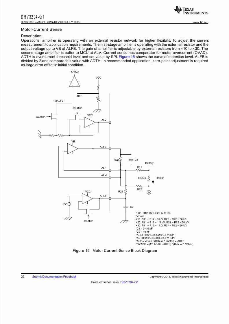
Motor-Current Sense
Description:
Operational amplifier is operating with an external resistor network for higher flexibility to adjust the currentmeasurement to application requirements. The first-stage amplifier is operating with the external resistor and theoutput voltage up to VB at ALFB. The gain of amplifier is adjustable by external resistors from ×10 to ×30. Thesecond-stage amplifier is buffer to MCU at ALV. Current sense has comparator for motor overcurrent (OVAD).
ADTH is overcurrent threshold level and set value by SPI. Figure 15 shows the curve of detection level. ALFB isdivided by 2 and compare this value with ADTH. In recommended application, zero-point adjustment is requiredas large error offset in initial condition.
Figure 15. Motor Current-Sense Block Diagram
22 Submit Documentation Feedback Copyright © 2013, Texas Instruments Incorporated
Product Folder Links :DRV3204-Q1
8/10/2019 Slvsbt3b Three-Phase Brushless Motor Driver
http://slidepdf.com/reader/full/slvsbt3b-three-phase-brushless-motor-driver 23/38
VCC
VO_0
VLine
=Y/ X
Imotor0A
X
Y
ADTH
Imotor0A OVAD
ALFB/2ALV
D R V 32 04 -Q 1www.ti.com SLVSBT3B – MARCH 2013– REVISED JULY 2013
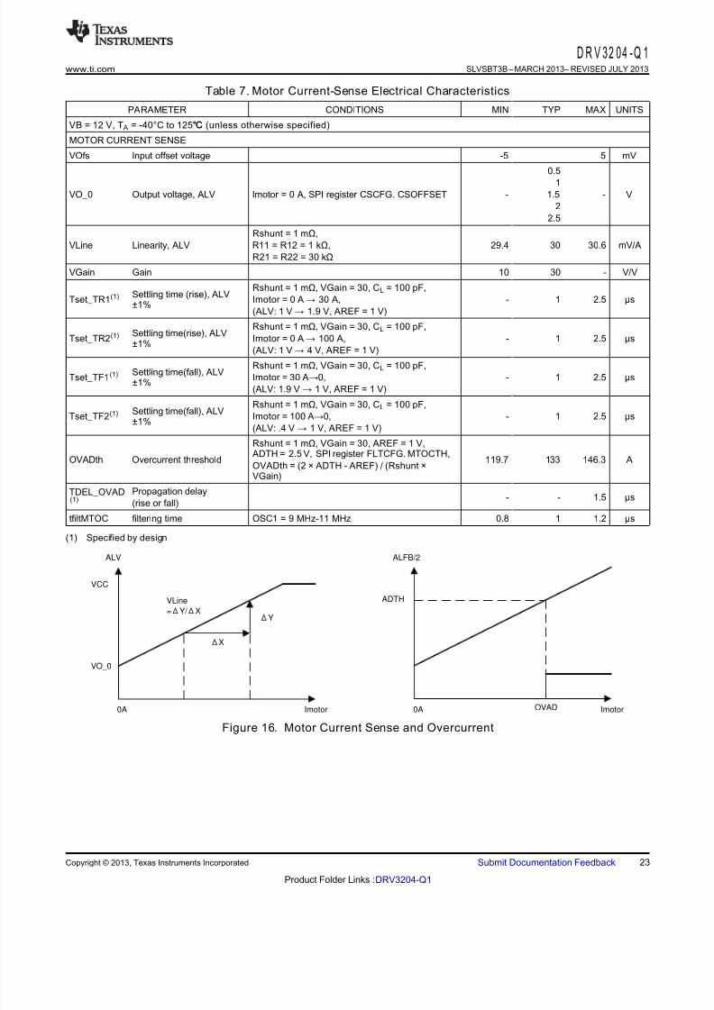
Table 7. Motor Current-Sense Electrical Characteristics
PARAMETER CONDITIONS MIN TYP MAX UNITS
VB = 12 V, T A = -40°C to 125℃℃ (unless otherwise specified)
MOTOR CURRENT SENSE
VOfs Input offset voltage -5 5 mV
0.5
1
VO_0 Output voltage, ALV Imotor = 0 A, SPI register CSCFG. CSOFFSET - 1.5 - V
2
2.5
Rshunt = 1 mΩ,
VLine Linearity, ALV R11 = R12 = 1 kΩ, 29.4 30 30.6 mV/A
R21 = R22 = 30 kΩ
VGain Gain 10 30 - V/V
Rshunt = 1 mΩ, VGain = 30, CL = 100 pF,Settling time (rise), ALV
Tset_TR1(1) Imotor = 0 A → 30 A, - 1 2.5 µs±1%
(ALV: 1 V → 1.9 V, AREF = 1 V)
Rshunt = 1 mΩ, VGain = 30, CL = 100 pF,Settling time(rise), ALV
Tset_TR2(1) Imotor = 0 A → 100 A, - 1 2.5 µs±1%
(ALV: 1 V → 4 V, AREF = 1 V)Rshunt = 1 mΩ, VGain = 30, CL = 100 pF,
Settling time(fall), ALVTset_TF1(1) Imotor = 30 A→0, - 1 2.5 µs
±1%(ALV: 1.9 V → 1 V, AREF = 1 V)
Rshunt = 1 mΩ, VGain = 30, CL = 100 pF,Settling time(fall), ALV
Tset_TF2(1) Imotor = 100 A→0, - 1 2.5 µs±1%
(ALV: .4 V → 1 V, AREF = 1 V)
Rshunt = 1 mΩ, VGain = 30, AREF = 1 V, ADTH = 2.5 V, SPI register FLTCFG. MTOCTH,
OVADth Overcurrent threshold 119.7 133 146.3 AOVADth = (2 × ADTH - AREF) / (Rshunt ×VGain)
Propagation delayTDEL_OVAD- - 1.5 µs(1)
(rise or fall)
tfiltMTOC filtering time OSC1 = 9 MHz-11 MHz 0.8 1 1.2 µs
(1) Specified by design
Figure 16. Motor Current Sense and Overcurrent
Copyright © 2013, Texas Instruments Incorporated Submit Documentation Feedback 23
Product Folder Links :DRV3204-Q1
8/10/2019 Slvsbt3b Three-Phase Brushless Motor Driver
http://slidepdf.com/reader/full/slvsbt3b-three-phase-brushless-motor-driver 24/38
Motor Current
MTOC SPI Register Flag
SPI Access
read write 1to clear
FAULT
Pre-Driver Enable Disable Enable
OVAD
OVADth
tfiltMTOCtfiltMTOC
D R V 32 04 -Q 1SLVSBT3B –MARCH 2013–REVISED JULY 2013 www.ti.com
(1) MCU must set the FLTCFG.FLGLATCH_EN bit to 1 to get the latch-type operation shown in this figure.
(2) When MTOC condition is detected, FAULT is asserted to low if FE_MTOC bit is 1.
(3) When MTOC condition is detected, Pre Driver is disabled if SE_MTOC is 1.
Figure 17. Motor Overcurrent Event
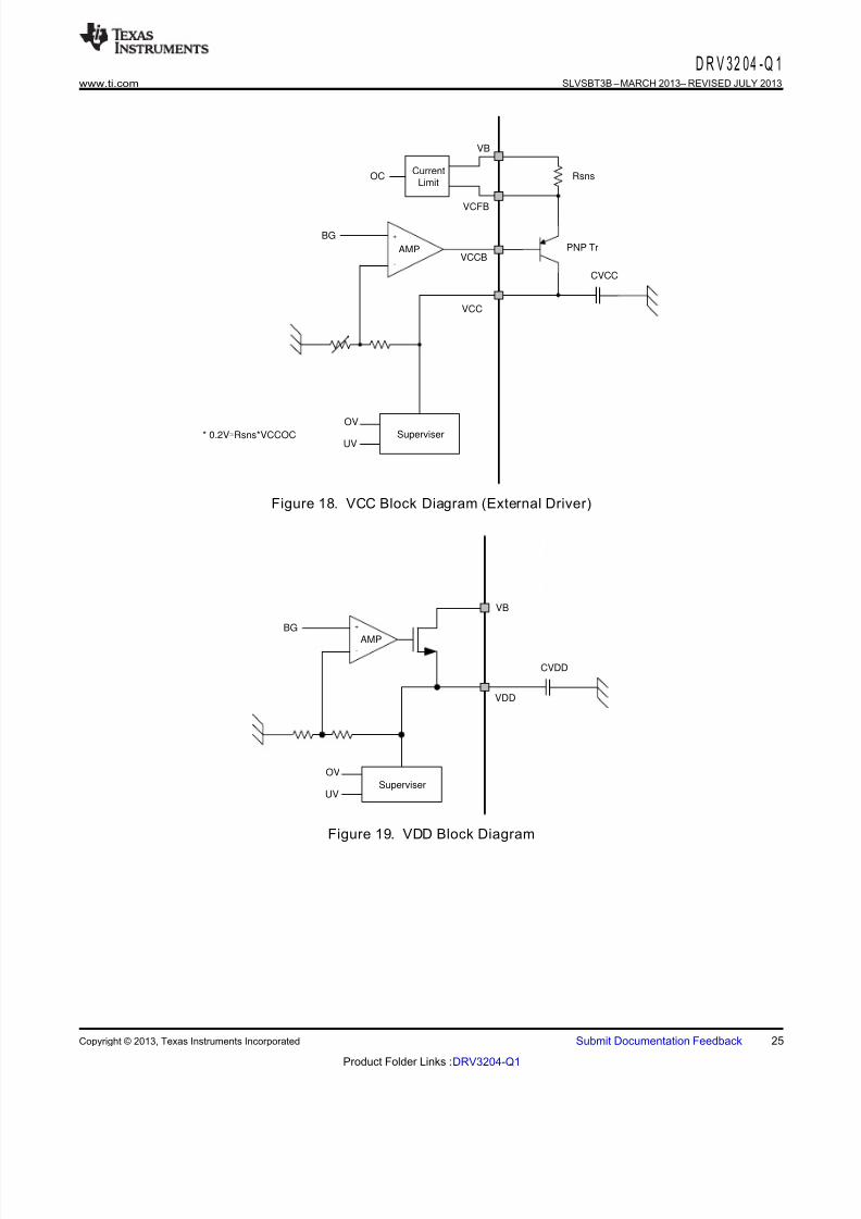
Regulators
Description:
The regulator block offers 5-V LDO and 3.3-V LDO. The VCC LDO regulates VB down to 5 V with an externalPNP controlled by the regulator block. This 5 V is supplied to MCU and other components.
The VDD regulator regulates VB down to 3.3 V with internal FET and controller. The 5 V LDO is protectedagainst short to GND fault. Overvoltage and under voltage events of both supplies are detected. The under voltage of the 5-V LDO is set by SPI.
24 Submit Documentation Feedback Copyright © 2013, Texas Instruments Incorporated
Product Folder Links :DRV3204-Q1
8/10/2019 Slvsbt3b Three-Phase Brushless Motor Driver
http://slidepdf.com/reader/full/slvsbt3b-three-phase-brushless-motor-driver 25/38
+
-
CVDD
VDD
AMP
BG
SuperviserUV
OV
VB
+
-
CVCC
VCC
AMP
VB
BG
SuperviserUV
CurrentLimit
OC
OV
VCFB
VCCB
Rsns
PNP Tr
* 0.2VRsns*VCCOC
D R V 32 04 -Q 1www.ti.com SLVSBT3B – MARCH 2013– REVISED JULY 2013
Figure 18. VCC Block Diagram (External Driver)
Figure 19. VDD Block Diagram
Copyright © 2013, Texas Instruments Incorporated Submit Documentation Feedback 25
Product Folder Links :DRV3204-Q1
8/10/2019 Slvsbt3b Three-Phase Brushless Motor Driver
http://slidepdf.com/reader/full/slvsbt3b-three-phase-brushless-motor-driver 26/38
D R V 32 04 -Q 1SLVSBT3B –MARCH 2013–REVISED JULY 2013 www.ti.com
Table 8. VCC and VDD Electrical Characteristics
PARAMETER CONDITIONS MIN TYP MAX UNITS
VB = 12 V, T A = -40°C to 125℃℃ (unless otherwise specified)
VCC
VCC1 Output Voltage 4.9 5 5.1 V
VCC2 Output Voltage VB = 4.5 V, ILVCC = 5 mA-150 mA 4.25 4.5 V
IBVCC Base Current 1.5 mA
hfePNP DC current gain of external PNP 100 - -
VLRVCC Load regulation ILVCC = 5 mA-150 mA -20 - 20 mV
CVCC External Capacitance 22 100 µF
RVCC ESR of external Capacitor 300 mΩ
3.7 4 4.3VCCUV Under voltage detection threshold SPI register FLTCFG. VCCUVTH V
3.9 4.2 4.5
VCCUVHYS Under voltage detection threshold hysteresis 50 100 200 mV
VCCOV Overvoltage detection threshold 6 6.5 7 V
VCCOC Current Limit Rsns = 0.51 Ω, 0.2 V ⋍ Rsns (1), VCCOC 300 400 550 mA
Tvcc1(2) Rise Time VCC > VCCUV, CVCC = 22 µF 0.5 ms
Tvcc2(2)
Rise Time VCC > VCCUV, CVCC = 100 µF 1.5 msVDD
VDD Output Voltage 3 3.3 3.6 V
CVDD Load Capacitance 1 µF
VDDUV Under voltage detection threshold 2.1 2.3 2.5 V
VDDOV Overvoltage detection threshold 4 4.3 4.6 V
Tvdd(2) Rise Time VDD > VDDUV, CVDD = 1 µF 100 µs
(1) No variation of the external components(2) Specified by design
26 Submit Documentation Feedback Copyright © 2013, Texas Instruments Incorporated
Product Folder Links :DRV3204-Q1
8/10/2019 Slvsbt3b Three-Phase Brushless Motor Driver
http://slidepdf.com/reader/full/slvsbt3b-three-phase-brushless-motor-driver 27/38
TSD
IPTAT
+
-VREF
VB
VB_OV
VB_UV
D R V 32 04 -Q 1www.ti.com SLVSBT3B – MARCH 2013– REVISED JULY 2013
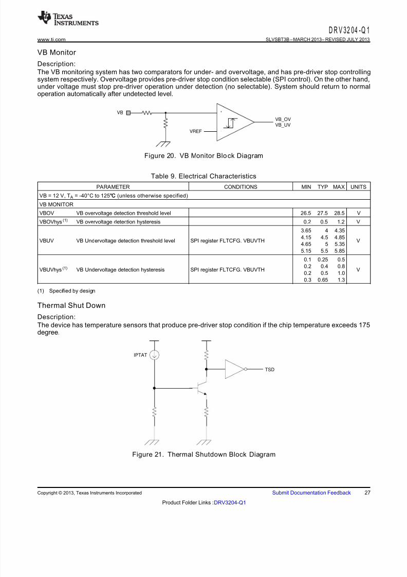
VB Monitor
Description:
The VB monitoring system has two comparators for under- and overvoltage, and has pre-driver stop controllingsystem respectively. Overvoltage provides pre-driver stop condition selectable (SPI control). On the other hand,under voltage must stop pre-driver operation under detection (no selectable). System should return to normaloperation automatically after undetected level.
Figure 20. VB Monitor Blo ck Diagram
Table 9. Electrical Characteristics
PARAMETER CONDITIONS MIN TYP MAX UNITS
VB = 12 V, T A = -40°C to 125℃℃ (unless otherwise specified)
VB MONITOR
VBOV VB overvoltage detection threshold level 26.5 27.5 28.5 V
VBOVhys (1) VB overvoltage detection hysteresis 0.2 0.5 1.2 V
3.65 4 4.35
4.15 4.5 4.85VBUV VB Undervoltage detection threshold level SPI register FLTCFG. VBUVTH V
4.65 5 5.35
5.15 5.5 5.85
0.1 0.25 0.5
0.2 0.4 0.8VBUVhys (1) VB Undervoltage detection hysteresis SPI register FLTCFG. VBUVTH V
0.2 0.5 1.0
0.3 0.65 1.3
(1) Specified by design
Thermal Shut Down
Description:
The device has temperature sensors that produce pre-driver stop condition if the chip temperature exceeds 175degree.
Figure 21. Thermal Shutdown Block Diagram
Copyright © 2013, Texas Instruments Incorporated Submit Documentation Feedback 27
Product Folder Links :DRV3204-Q1

8/10/2019 Slvsbt3b Three-Phase Brushless Motor Driver
http://slidepdf.com/reader/full/slvsbt3b-three-phase-brushless-motor-driver 28/38
VREF
OSC1(OSC2)
D R V 32 04 -Q 1SLVSBT3B –MARCH 2013–REVISED JULY 2013 www.ti.com
Table 10. Electrical Characteristics
PARAMETER CONDITIONS MIN TYP MAX UNITS
VB = 12 V, T A = -40°C to 125℃℃ (unless otherwise specified)
THERMAL SHUT DOWN
TSD(1) Thermal shut down threshold level 155 175 195 °C
TSDhys(1) Thermal shut down hysteresis 5 10 15 °C
(1) Specified by design
Oscillator
Description:
Oscillator block generates two 10-MHZ clock signals. OSC1 is the primary clock used for internal logicsynchronization and timing control. OSC2 is the secondary clock used to monitor the status of OSC1.
Figure 22. Oscillator Block Diagram
Table 11. Oscillator Electrical CharacteristicsPARAMETER CONDITIONS MIN TYP MAX UNITS
VB = 12 V, T A = -40°C to 125℃℃ (unless otherwise specified)
OSCILLATOR
OSC1 OSC1 frequency 9 10 11 MHz
OSC2 OSC2 frequency 10 MHz
28 Submit Documentation Feedback Copyright © 2013, Texas Instruments Incorporated
Product Folder Links :DRV3204-Q1
8/10/2019 Slvsbt3b Three-Phase Brushless Motor Driver
http://slidepdf.com/reader/full/slvsbt3b-three-phase-brushless-motor-driver 29/38
VDD VCC
RES
Level Shift
VCC
R_RES
VCC
VDD VCC
Level Shift
VCC
DOUT
EN
VDD VCC
Level Shift
VCC
FAULT
VCC VDD
Level Shift
VDD
DIN
SCK
CTLxxTEST
VCC VDD
Level Shift
VDD
CS
PRN
VCC
Ru
Rd
V5INT
ENABLE
Rd
CLAMPV5INT
D R V 32 04 -Q 1www.ti.com SLVSBT3B – MARCH 2013– REVISED JULY 2013
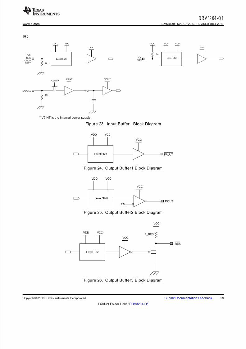
I/O
* V5INT is the internal power supply.
Figure 23. Input Buffer1 Block Diagram
Figure 24. Output Buffer1 Block Diagram
Figure 25. Output Buffer2 Block Diagram
Figure 26. Output Buffer3 Block Diagram
Copyright © 2013, Texas Instruments Incorporated Submit Documentation Feedback 29
Product Folder Links :DRV3204-Q1
8/10/2019 Slvsbt3b Three-Phase Brushless Motor Driver
http://slidepdf.com/reader/full/slvsbt3b-three-phase-brushless-motor-driver 30/38
Sleep
VCCVDD
Band GapCharge Pump
Enable
VB
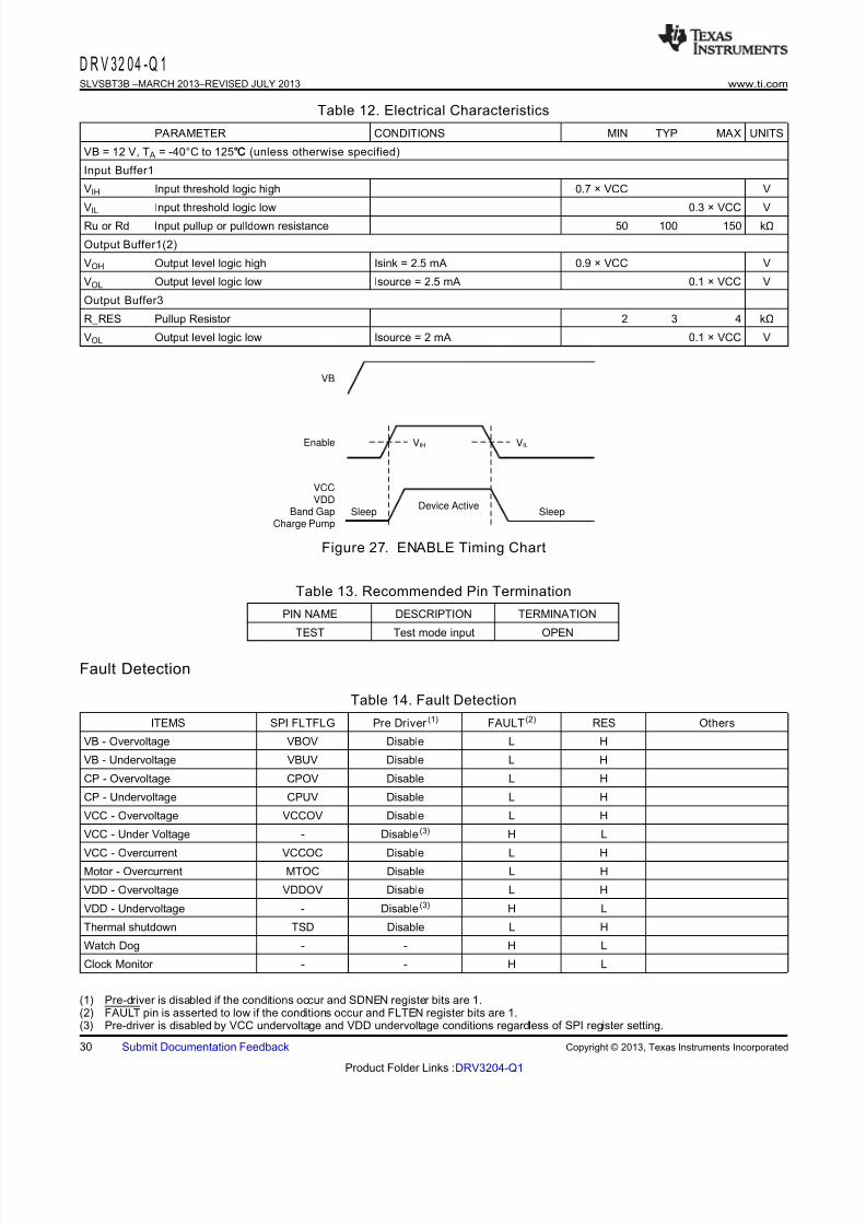
VIH VIL
Device ActiveSleep
D R V 32 04 -Q 1SLVSBT3B –MARCH 2013–REVISED JULY 2013 www.ti.com
Table 12. Electrical Characteristics
PARAMETER CONDITIONS MIN TYP MAX UNITS
VB = 12 V, T A = -40°C to 125℃℃ (unless otherwise specified)
Input Buffer1
VIH Input threshold logic high 0.7 × VCC V
VIL
Input threshold logic low 0.3 × VCC V
Ru or Rd Input pullup or pulldown resistance 50 100 150 kΩ
Output Buffer1(2)
VOH Output level logic high Isink = 2.5 mA 0.9 × VCC V
VOL Output level logic low Isource = 2.5 mA 0.1 × VCC V
Output Buffer3
R_RES Pullup Resistor 2 3 4 kΩ
VOL Output level logic low Isource = 2 mA 0.1 × VCC V
Figure 27. ENABLE Timing Chart
Table 13. Recommended Pin Termination
PIN NAME DESCRIPTION TERMINATION
TEST Test mode input OPEN
Fault Detection
Table 14. Fault Detection
ITEMS SPI FLTFLG Pre Driver (1) FAULT (2) RES Others
VB - Overvoltage VBOV Disable L H
VB - Undervoltage VBUV Disable L H
CP - Overvoltage CPOV Disable L H
CP - Undervoltage CPUV Disable L H
VCC - Overvoltage VCCOV Disable L H
VCC - Under Voltage - Disable (3) H L
VCC - Overcurrent VCCOC Disable L H
Motor - Overcurrent MTOC Disable L H
VDD - Overvoltage VDDOV Disable L H
VDD - Undervoltage - Disable (3) H L
Thermal shutdown TSD Disable L H
Watch Dog - - H L
Clock Monitor - - H L
(1) Pre-driver is disabled if the conditions occur and SDNEN register bits are 1.(2) FAULT pin is asserted to low if the conditions occur and FLTEN register bits are 1.(3) Pre-driver is disabled by VCC undervoltage and VDD undervoltage conditions regardless of SPI register setting.
30 Submit Documentation Feedback Copyright © 2013, Texas Instruments Incorporated
Product Folder Links :DRV3204-Q1
8/10/2019 Slvsbt3b Three-Phase Brushless Motor Driver
http://slidepdf.com/reader/full/slvsbt3b-three-phase-brushless-motor-driver 31/38
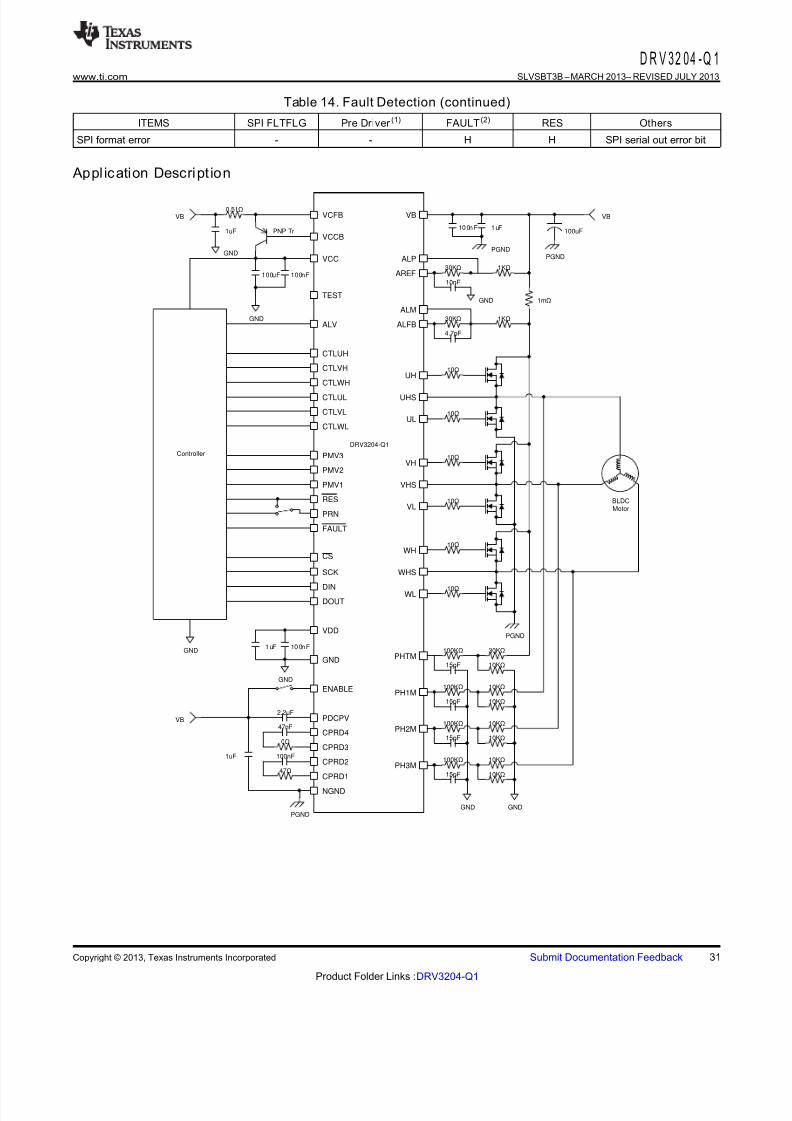
CTLWL
VCC
PMV2
PMV3
AREF
ALFB
ALP
ALM
ALV
VCFB
VCCB
PMV1
ENABLE
VB
CS
VDD
DOUT
GND PHTM
PH1M
PH2M
PH3M
RES
CTLVL
CTLUL
WL
VL
UL
CTLWH
CTLVH
CTLUH
TEST
WH
WHS
FAULT
PRN
DIN
SCK
VHS
VH
UHS
PDCPV
UH
CPRD4
CPRD3
CPRD2
CPRD1
NGND
10nF
4.7pF
30K
30K 1K
1K
10
10
10K
30K
100K 10K
10K
10K
10K
10K
10K15pF
15pF
15pF
100K
100K
100nF 1uF100uF
VB
1m
100K
100uF 100nF
VB
1uF 100nF
VB
10
10
10
10
47nF
0
100nF
47
15pF
2.2uF
PNP Tr
0.51
1uF
GND
GND
PGND
GND
GNDPGND
GND
BLDCMotor
PGNDGND
GND
PGND
Controller
DRV3204-Q1
1uF
D R V 32 04 -Q 1www.ti.com SLVSBT3B – MARCH 2013– REVISED JULY 2013
Table 14. Fault Detection (continued)
ITEMS SPI FLTFLG Pre Driver (1) FAULT (2) RES Others
SPI format error - - H H SPI serial out error bit
Appl ic ation Descri pt io n
Copyright © 2013, Texas Instruments Incorporated Submit Documentation Feedback 31
Product Folder Links :DRV3204-Q1
8/10/2019 Slvsbt3b Three-Phase Brushless Motor Driver
http://slidepdf.com/reader/full/slvsbt3b-three-phase-brushless-motor-driver 32/38
D R V 32 04 -Q 1SLVSBT3B –MARCH 2013–REVISED JULY 2013 www.ti.com
REVISION HISTORY
Changes from Revision A (March 2013) to Revision B Page
• Changed Operation VB Range in Features .......................................................................................................................... 1
• Changed Applications from automotive to include specific pump applications .................................................................... 1
• Deleted EEPROM going into the Control Logic from the Top Block Diagram ...................................................................... 4• Added VB3 parameter to the SUPPLY VOLTAGE AND CURRENT table and added corresponding table note (2) ............ 5
• Changed ACE-Q100 from Grade 0 to Grade 1 in table note (1) of SUPPLY VOLTAGE AND CURRENT ........................... 5
• Changed Charge-Pump Block Diagram by moving line to connection by VF .................................................................... 17
• Added PDCPV to all output voltage parameters in the Charge-Pump Electrical Characteristics table .............................. 17
• Changed VGain max value to the typ value in the Motor Current-Sense Electrical Characteristics table ......................... 23
• Added UNIT of VGain in the Motor Current-Sense Electrical Characteristics table ........................................................... 23
• Changed VDD Block Diagram by removing OC current limit and resistor to VB ............................................................... 25
• Added VBOVhys parameter to the VB Monitor table and added corresponding table note (1) ........................................... 27
• Added VBUVhys parameter to the VB Monitor table and added corresponding table note (1) ........................................... 27
• Changed Application Description image by moving connecting line between UH, UHS, and UL ...................................... 31
32 Submit Documentation Feedback Copyright © 2013, Texas Instruments Incorporated
Product Folder Links :DRV3204-Q1
8/10/2019 Slvsbt3b Three-Phase Brushless Motor Driver
http://slidepdf.com/reader/full/slvsbt3b-three-phase-brushless-motor-driver 33/38
PACKAGE OPTION ADDENDUM
www.ti.com 7-Jan-2014
Addendum-Page 1
PACKAGING INFORMATION
Orderable Device Status
(1)
Package Type PackageDrawing
Pins PackageQty
Eco Plan
(2)
Lead/Ball Finish
(6)
MSL Peak Temp
(3)
Op Temp (°C) Device Marking
(4/5)
DRV3204QPHPQ1 ACTIVE HTQFP PHP 48 1 Green (RoHS
& no Sb/Br)
CU NIPDAU Level-3-260C-168 HR -40 to 150 DRV3204
(1)
The marketing status values are defined as follows:ACTIVE: Product device recommended for new designs.LIFEBUY: TI has announced that the device will be discontinued, and a lifetime-buy period is in effect.
NRND: Not recommended for new designs. Device is in production to support existing customers, but TI does not recommend using this part in a new design.PREVIEW: Device has been announced but is not in production. Samples may or may not be available.OBSOLETE: TI has discontinued the production of the device.
(2)
Eco Plan - The planned eco-friendly classification: Pb-Free (RoHS), Pb-Free (RoHS Exempt), or Green (RoHS & no Sb/Br) - please check http://www.ti.com/productcontent for the latest availabilityinformation and additional product content details.TBD: The Pb-Free/Green conversion plan has not been defined.Pb-Free (RoHS): TI's terms "Lead-Free" or "Pb-Free" mean semiconductor products that are compatible with the current RoHS requirements for all 6 substances, including the requirement thatlead not exceed 0.1% by weight in homogeneous materials. Where designed to be soldered at high temperatures, TI Pb-Free products are suitable for use in specified lead-free processes.Pb-Free (RoHS Exempt): This component has a RoHS exemption for either 1) lead-based flip-chip solder bumps used between the die and package, or 2) lead-based die adhesive used betweenthe die and leadframe. The component is otherwise considered Pb-Free (RoHS compatible) as defined above.Green (RoHS & no Sb/Br): TI defines "Green" to mean Pb-Free (RoHS compatible), and free of Bromine (Br) and Antimony (Sb) based flame retardants (Br or Sb do not exceed 0.1% by weightin homogeneous material)
(3)
MSL, Peak Temp. - The Moisture Sensitivity Level rating according to the JEDEC industry standard classifications, and peak solder temperature.
(4)
There may be additional marking, which relates to the logo, the lot trace code information, or the environmental category on the device.
(5)
Multiple Device Markings will be inside parentheses. Only one Device Marking contained in parentheses and separated by a "~" will appear on a device. If a line is indented then it is a continuationof the previous line and the two combined represent the entire Device Marking for that device.
(6)
Lead/Ball Finish - Orderable Devices may have multiple material finish options. Finish options are separated by a vertical ruled line. Lead/Ball Finish values may wrap to two lines if the finishvalue exceeds the maximum column width.
Important Information and Disclaimer:The information provided on this page represents TI's knowledge and belief as of the date that it is provided. TI bases its knowledge and belief on informationprovided by third parties, and makes no representation or warranty as to the accuracy of such information. Efforts are underway to better integrate information from third parties. TI has taken andcontinues to take reasonable steps to provide representative and accurate information but may not have conducted destructive testing or chemical analysis on incoming materials and chemicals.TI and TI suppliers consider certain information to be proprietary, and thus CAS numbers and other limited information may not be available for release.
In no event shall TI's liability arising out of such information exceed the total purchase price of the TI part(s) at issue in this document sold by TI to Customer on an annual basis.
8/10/2019 Slvsbt3b Three-Phase Brushless Motor Driver
http://slidepdf.com/reader/full/slvsbt3b-three-phase-brushless-motor-driver 34/38
PACKAGE OPTION ADDENDUM
www.ti.com 7-Jan-2014
Addendum-Page 2
8/10/2019 Slvsbt3b Three-Phase Brushless Motor Driver
http://slidepdf.com/reader/full/slvsbt3b-three-phase-brushless-motor-driver 35/38
8/10/2019 Slvsbt3b Three-Phase Brushless Motor Driver
http://slidepdf.com/reader/full/slvsbt3b-three-phase-brushless-motor-driver 36/38
8/10/2019 Slvsbt3b Three-Phase Brushless Motor Driver
http://slidepdf.com/reader/full/slvsbt3b-three-phase-brushless-motor-driver 37/38
8/10/2019 Slvsbt3b Three-Phase Brushless Motor Driver
http://slidepdf.com/reader/full/slvsbt3b-three-phase-brushless-motor-driver 38/38
IMPORTANT NOTICE
Texas Instruments Incorporated and its subsidiaries (TI) reserve the right to make corrections, enhancements, improvements and other changes to its semiconductor products and services per JESD46, latest issue, and to discontinue any product or service per JESD48, latestissue. Buyers should obtain the latest relevant information before placing orders and should verify that such information is current andcomplete. All semiconductor products (also referred to herein as “components”) are sold subject to TI’s terms and conditions of salesupplied at the time of order acknowledgment.
TI warrants performance of its components to the specifications applicable at the time of sale, in accordance with the warranty in TI’s terms
and conditions of sale of semiconductor products. Testing and other quality control techniques are used to the extent TI deems necessaryto support this warranty. Except where mandated by applicable law, testing of all parameters of each component is not necessarilyperformed.
TI assumes no liability for applications assistance or the design of Buyers’ products. Buyers are responsible for their products andapplications using TI components. To minimize the risks associated with Buyers’ products and applications, Buyers should provideadequate design and operating safeguards.
TI does not warrant or represent that any license, either express or implied, is granted under any patent right, copyright, mask work right, or other intellectual property right relating to any combination, machine, or process in which TI components or services are used. Informationpublished by TI regarding third-party products or services does not constitute a license to use such products or services or a warranty or endorsement thereof. Use of such information may require a license from a third party under the patents or other intellectual property of thethird party, or a license from TI under the patents or other intellectual property of TI.
Reproduction of significant portions of TI information in TI data books or data sheets is permissible only if reproduction is without alterationand is accompanied by all associated warranties, conditions, limitations, and notices. TI is not responsible or liable for such altereddocumentation. Information of third parties may be subject to additional restrictions.
Resale of TI components or services with statements different from or beyond the parameters stated by TI for that component or service
voids all express and any implied warranties for the associated TI component or service and is an unfair and deceptive business practice.TI is not responsible or liable for any such statements.
Buyer acknowledges and agrees that it is solely responsible for compliance with all legal, regulatory and safety-related requirementsconcerning its products, and any use of TI components in its applications, notwithstanding any applications-related information or supportthat may be provided by TI. Buyer represents and agrees that it has all the necessary expertise to create and implement safeguards whichanticipate dangerous consequences of failures, monitor failures and their consequences, lessen the likelihood of failures that might causeharm and take appropriate remedial actions. Buyer will fully indemnify TI and its representatives against any damages arising out of the useof any TI components in safety-critical applications.
In some cases, TI components may be promoted specifically to facilitate safety-related applications. With such components, TI’s goal is tohelp enable customers to design and create their own end-product solutions that meet applicable functional safety standards andrequirements. Nonetheless, such components are subject to these terms.
No TI components are authorized for use in FDA Class III (or similar life-critical medical equipment) unless authorized officers of the partieshave executed a special agreement specifically governing such use.
Only those TI components which TI has specifically designated as military grade or “enhanced plastic” are designed and intended for use inmilitary/aerospace applications or environments. Buyer acknowledges and agrees that any military or aerospace use of TI componentswhich have n ot been so designated is solely at the Buyer's risk, and that Buyer is solely responsible for compliance with all legal andregulatory requirements in connection with such use.
TI has specifically designated certain components as meeting ISO/TS16949 requirements, mainly for automotive use. In any case of use of non-designated products, TI will not be responsible for any failure to meet ISO/TS16949.
Products Applications
Audio www.ti.com/audio Automotive and Transportation www.ti.com/automotive
Amplifiers amplifier.ti.com Communications and Telecom www.ti.com/communications
Data Converters dataconverter.ti.com Computers and Peripherals www.ti.com/computers
DLP® Products www.dlp.com Consumer Electronics www.ti.com/consumer-apps
DSP dsp.ti.com Energy and Lighting www.ti.com/energy
Clocks and Timers www.ti.com/clocks Industrial www.ti.com/industrial
Interface interface.ti.com Medical www.ti.com/medical
Logic logic.ti.com Security www.ti.com/security
Power Mgmt power.ti.com Space, Avionics and Defense www.ti.com/space-avionics-defenseMicrocontrollers microcontroller.ti.com Video and Imaging www.ti.com/video
RFID www.ti-rfid.com
OMAP Applications Processors www.ti.com/omap TI E2E Community e2e.ti.com
Wireless Connectivity www.ti.com/wirelessconnectivity
Mailing Address: Texas Instruments, Post Office Box 655303, Dallas, Texas 75265Copyright © 2014, Texas Instruments Incorporated