small signal analysis of the lcc-type parallel...
TRANSCRIPT

Small Signal Analysis of theLCC-Type Parallel ResonantConverter
ISSA BATARSEH, Senior Member, IEEE
C. MEGALEMOSUniversity of Central Florida
M. SZNAIER, Member, IEEEPennsylvania State University
In this paper, the small signal analysis of the LCC-type
parallel resonant converter (LCC-PRC) operating in the
continuous conduction mode is given. This analysis is based on
both the state-plane diagram, which has been successfully used
to obtain the steady state response for resonant converters,
and the Taylor series expansion. Applying perturbation directly
to the steady state trajectory, a discrete small signal model
for the converter can be derived in terms of the input voltage,
switching frequency, and the converter state variables. Based on
this analysis, closed-loop form solutions for the input-to-output
and control-to-output transfer functions are derived. It is shown
that the theoretical and computer simulation results are in full
agreement.
Manuscript received February 7, 1994; revised January 23, 1995.
IEEE Log No. T-AES/32/2/03451.
Authors’ addresses: I. Batarseh and C. Megalemos, Dept. ofElectrical and Computer Engineering, University of Central Florida,Orlando, FL 32816, email: [email protected]; M. Sznaier,Electrical Engineering Department, Pennsylvania State University,University Park, PA 16802.
0018-9251/96/$10.00 c° 1996 IEEE
I. INTRODUCTION
To achieve the desired system stability, theopen-loop control-to-output frequency response isused to analytically design the transfer function ofthe control circuit. Furthermore, the characterizationof the closed-loop small signal performance dueto the line voltage is necessary to predeterminethe open-loop line-to-output frequency response.Depending on the complexity of the convertertopology and circuit component models used for theconverter power stage, these frequency responsesmay be obtained experimentally, numerically, oranalytically. Experimental measurements of theconverter frequency responses become necessarywhen the converter power stage is known as a blackbox. On the other hand, if the circuit topology aswell as the control technique of the converter powerstage are known, then the power stage responses canbe simulated numerically, thus avoiding the costlyconstruction of the converter power stage. However,due to highly intensive computations, this method istime consuming. Hence, it is worthwhile to derive theanalytical solutions so that excessive time and expensein the experimental approach can be avoided. It ismore efficient to utilize analytical solutions for thepower stage responses in the systematic design of acontrol circuit.To avoid costly construction and debugging of
converter prototypes based on the trial and errorapproach, analytical methods to obtain the smallsignal frequency responses for dc-to-dc convertershave been developed [1—24]. The analytical smallsignal frequency responses help a circuit designerchoose a proper compensation circuit or debug thedesign of the converter power stage from its steadystate characteristics so that the small signal frequencyresponses of the revised converter and the selectedcompensation circuit are compatible for attaining thedesired system stability. For many years, publishedwork in this area has been focused on the pulsewidthmodulation (PWM) converters [1—12]. In recent years,however, the small signal analysis of dc-to-dc resonantconverters have been investigated by many researchersin this field [12—24]. Thus far, the analysis to achievethe small signal behavior is limited to second-orderseries and parallel resonant converters (PRCs)[13—22], with little work done on high-order resonantconverters [23, 24]. This analysis is complicated in itsmathematics and obscure in its physical insight into theconverter operation due to a stringent time-domainanalysis. An alternative analytical method is neededto easily visualize the small signal behavior around theconverter steady state trajectory and to allow furthergeneralization to a larger class of resonant converters.The steady state analyses for numerous resonant
converter topologies have been thoroughly investigatedin the literature. The steady state responses of these
702 IEEE TRANSACTIONS ON AEROSPACE AND ELECTRONIC SYSTEMS VOL. 32, NO. 2 APRIL 1996

converters are known and in most cases have beenrepresented by closed trajectories in the state-planediagram [19, 21, 28—31]. Since the state-plane diagramsof resonant converters in general consist of only a fewwell defined simple geometric curves in the state-plane,it is possible to develop a generalized computerprogram from which the frequency responses of aresonant converter can be derived once its state-planediagram is specified. Hence, this technique can begeneralized to any resonant converter topology onceits state-plane trajectory is known. Moreover, by usingthe state-plane diagram approach, more physical insightinto the converter dynamic behavior can be obtained.This is because the perturbation is done graphically onthe state-plane diagram with the actual displacementof the converter state variables, as well as input andcontrol parameters, being observed.The analysis method was first used to achieve
the discrete small signal models of the conventionalseries resonant converter (SRC) and PRC undervariable switching frequency control in [19] and[23] respectively. In this analysis technique, theinitial perturbations on the converter state variables,the control and source inputs, were made on thestate-plane diagram to produce the perturbedstate trajectories. Then, using the geometricalrelation between the steady state and the perturbedtrajectories and applying the superposition theorem,the perturbation response can be written as a linearcombination of those initial perturbations. Observingthe differences between the steady-state and theperturbed trajectories that are constructed on thesame state-plane, we can attain better understandingof the converter small signal behavior. The discretesmall signal models of these resonant convertersare developed without the time-averaging of theoutput waveform. When the converter operates inthe continuous conduction mode (CCM), the discretesmall signal model can correctly predict small signalfrequency response because the same set of theperturbed states exists at any given time and theseperturbed states possess their continuities throughoutthe converter operation. This technique is applied toobtain the frequency response for the well-knownLCC-type PRC. Its steady state analysis has beenthoroughly analyzed in the literature [25—28]. Once thesmall signal model of the converter is obtained, thenits closed-loop compensation can be properly designedand simulated before actually building the converter.The steady state analysis and the derivation of
the state-plane diagram for the LCC-type PRC isbriefly discussed in Section II. Section III providesthe mathematical development of the small signalanalysis. Using Taylor series expansion coupled withthe symmetry in steady state state-plane response, wederive the line-to-output and the control-to-outputtransfer functions. Consequently, the frequencyresponses can be computed from these functions.
Fig. 1. Simplified circuit of LCC-type PRC.
Since it is always possible to decompose any orderdc-to-dc resonant converters into many decoupledtwo-dimensional state-plane by using state-variabletransformation technique, the small signal analysispresented here is based on two-dimensional state-planediagram [29]. By using the state-plane diagramapproach, more physical insight into the converterdynamic behavior can be obtained. This is becausethe perturbation is done graphically on the state-planediagram with the actual displacements of the converterstate variables and input and control parametersobserved. To verify our theoretical work, computersimulation results are presented in Section IV and arecompared to the theoretical ones.
II. STEADY STATE ANALYSIS
In order to analytically obtain the small signalresponse of a resonant converter, it is necessary thatits dc operating conditions be known. Using this steadystate trajectory, a geometrical approach can be usedto derive the small signal frequency response modelof the converter. In this section, steady state analysisthat is based on the state-plane diagram will be brieflydiscussed. The objective here is to express the steadystate parameters of the converter in terms of theinitial switching points of the state-plane trajectory.Once such expressions are obtained, then perturbationsignals on these state-variable parameters are injecteddirectly into the state-plane diagram.The idealized circuit of the LCC-type PRC
(PRC-LCC) is shown in Fig. 1. The detailed steadystate analysis of the converter can be found in [26—29].Throughout the analysis, it is assumed that theresonant circuit is lossless and the switching devicesand diodes are ideal. When the converter operatesunder CCM with 50% duty ratio over one switchingperiod Ts, it can be shown that the effect of switchingof transistor/diode pairs can be represented by anequivalent square wave voltage source vs(t) withmagnitudes +Vg and ¡Vg. Moreover, assuming verylarge L0, the input current to the full-bridge rectifier,iE(t), may be presented by a dependent current sourceof magnitudes +I0 and ¡I0, depending on whether
BATARSEH ET AL.: SMALL SIGNAL ANALYSIS OF THE LCC-TYPE PARALLEL RESONANT CONVERTER 703

Fig. 2. Equivalent model of Fig. 1.
vcp(t) is greater or less than zero, respectively. Hence,the resultant equivalent circuit model is shown inFig. 2 from which the following differential equationsare obtained,
dil(t)dt
=1L[vs(t)¡ vcs(t)¡ vcp(t)] (1)
dvcp(t)
dt=1Cp[il(t)¡ iE(t)] (2)
dvcs(t)dt
=1Cs
l(t): (3)
Defining a new state variable, vc(t) = vcp(t) + vcs(t),then (1)—(3) can be rewritten as follows,
dildt=1L[vs(t)¡ vc(t)] (4)
dvcdt=1CT
"il(t)¡
iE(t)(1+Cp=Cs)
#(5)
where CT is the total capacitance given by
1CT
=1Cp+1Cs
dvcdil
=L
CT
il¡iE
(1+Cp=Cs)
vs¡ vc:
(6)
From (4) and (5), the state-plane equation in termsof vc(t) and i1(t) is given by, (6) can be expressed interms of the normalized state-plane equation in thefollowing form,
dvnc(t)dinl(t)
=inl(t)¡ i0nE(t)vns(t)¡ vnc(t)
(7)
where
vnc(t) = vc(t)=Vg vns(t) = vs(t)=Vg
inl(t) = Z0il(t)=Vg inE(t) = Z0iE(t)=Vg
i0nE(t) =
"1¡μ!0s!0
¶2#inE(t)
and the characteristic impedance Z0, and resonantfrequencies !0 and !0s are given by
Z0 =
sL
CT, !0 =
1pLCT
and !0s =1pLCs
:
Fig. 3. Typical state-plane trajectory for LCC-PRC.
It can be shown that the solution of (7) consists offour circular arcs in the inl¡ vnc state-plane with eachsingular point [vns, i
0nE] corresponds to one of the
following intervals,
[vns, i0nE] =
8>>><>>>:(+Vng,¡I0n0) t0 · t < t1(+Vng,+I
0n0) t1 · t < t0 +Ts=2 = t2
(¡Vng,+I0n0) t2 · t < t3(¡Vng,¡I0n0) t3 · t < t0 +Ts
(8)where Vng = vg=Vg. In steady state, Vng = 1.Typical inl¡ vnc state-plane diagram is illustrated
in Fig. 3. Detailed derivation of this figure is given in[28]. In this figure, ¯1 is the angular displacement ofthe trajectory when T1 is turned on with vcp < 0, ¯2is the angular displacement of the trajectory whenT1 is conducting with vcp > 0, and ® is the angulardisplacement when D1 is conducting. These angles arerelated to the switching and resonant frequencies by,
° = ¯1 +¯2 +®=!0Ts2=f0fs¼ =
¼
fns(9)
where fs and f0 are the switching and resonantfrequencies, respectively, and the normalized frequencyis defined by fns = fs=f0 with f0 = !0=2¼. The solutionof (7) consists of four circular arcs in the vnc¡ inlstate-plane given by
(vnC ¡ vns)2 + (inL¡ inE)2 = V2nmi (10)
where i= 1, 2, 3, and 4 and Vnmi are the radii whichare given by
Vnmi =
½Vnm1 for t0 · t < t1 or t0 +Ts=2 · t3Vnm2 for t1 · t < t0 +Ts=2 or t3 · t < t0 +Ts
:
(11)
From the state-plane diagram, it can be shown that
Vnm1 =q(Vng ¡ vnC(t0))2 + (inL(t0)+ In0)2 (12)
Vnm2 =q(inL(t1)¡ In0)2 +V2ng : (13)
704 IEEE TRANSACTIONS ON AEROSPACE AND ELECTRONIC SYSTEMS VOL. 32, NO. 2 APRIL 1996

The dc output voltage V0 is obtained by taking theaverage value of the resonant capacitor voltage, vcp,to yield
V0 =1°
"1¡μ!0s!0
¶2#[(°¡ 2¯1)Vg +2Z0il(t1)]
(14)where
¯1 = !0(t1¡ t0):The converter gain is obtained by normalizing (14) togive
M =V0Vg=1°
"1¡μ!0s!0
¶2#[(°¡ 2¯1)+2inl(t1)]:
(15)
Since the steady state analysis shown here is only forthe PRC-LCC operating in the natural commutationmode, inl(t0) must be positive and it can be expressedas
inl(t0) =
sI2n0 +
μ1I2n0¡ 1¶v2nC(t0) ¡ In0: (16)
For the converter design, it is more convenient toexpress the output voltage and converter gain in termsof the initial switching points vnc(t0) or inl(t0) insteadof inl(t1). From the state-plane diagram given in Fig.3, it can be shown that the following relation can beobtained,
inl(t1) =¡vnc(t0)I0n0
: (17)
Substituting (17) into (15), the converter gain becomes
M =1°
"1¡μ!0s!0
¶2#·(°¡ 2¯1)¡
2vnc(t0)I 0n0
¸: (18)
Finally, we need to express the switching angles ¯1,¯2, ®, and ° in terms of the initial switching point[vnc(t0), inl(t0)]. This can be accomplished from thestate-plane diagram given in Fig. 3 to obtain thefollowing relations,
¯1 = tan¡1 inl(t1)+ I
0n0
1¡ vnc(t1)¡ tan¡1 inl(t0)+ I
0n0
1¡ vnc(t0)(19)
¯2 +® =3¼2¡ tan¡1 inl(t1)¡ I
0n0
1¡ vnc(t1)¡ tan¡1 inl(t0)+ I
0n0
1+ vnc(t0):
(20)
Using (9), (19), and (20), the following functionalexpression for ° can be obtained as follows,
° = °[vnc(t0), inl(t0),I0n0,!0=!0s]: (21)
For the converter design, given !0=!0s, we maycalculate I 0n0, M, and ° once the initial switching point[vnc(t0), inl(t0)] is known. In the following section,based on the steady state equations derived in SectionII, we derive the small signal model by injectingperturbation to the state-variables of the state-plane.
Fig. 4. Converter block diagram under line and control signalsperturbations.
III. SMALL SIGNAL ANALYSIS
As shown in Section II, when the converterresponse is in steady state, the trajectory of its statevariables forms a unique closed contour for everyswitching period with stable dc values. However, theconverter trajectory can deviate from this uniquecontour due to disturbances on the line and controlinputs. In such a case, the trajectory becomes aperturbed trajectory. Under small signal perturbation,the excursion of the perturbed trajectory from thesteady state trajectory can be physically observedon the state-plane diagram [22, 23]. Physically,the small signal excursions from the steady statetrajectory can be observed as the perturbed trajectoryperiodically shrinks and expands around the steadystate trajectory at the frequency of perturbation. Majorsources of perturbations are due to the input andfrequency variations. Fig. 4 shows a simplified blockdiagram for a closed-loop converter system under linevoltage vg, and control signal (switching frequency)fs, perturbations. Based on this model, we deriveclosed-form solutions for the line-to-output transferfunction H1(s) and control-to-output transfer functionH2(s) which are defined as follows,
H1(s) =v0vg
(22a)
H2(s) =v0fs: (22b)
In this section, based on the state-plane diagramand the generalized analysis presented in [21], thesmall signal analysis for the PRC-LCC when operatedin the CCM is derived. By introducing perturbationsto the converter state variables, controlled switchingfrequency, and the input voltage at the beginning ofa half switching period, we can obtain the perturbedresponse at the beginning of the next half switchingperiod by using Taylor series expansion. Based on thistechnique, a closed form solution for H1(s) and H2(s) isderived from which we obtain the frequency response.
BATARSEH ET AL.: SMALL SIGNAL ANALYSIS OF THE LCC-TYPE PARALLEL RESONANT CONVERTER 705

Fig. 5. Perturbed steady state trajectory of Fig. 3.
Under small signal perturbations, we define kth and(k+1)th as trajectories in the first and second halfswitching cycles of the state-plane diagram of Fig. 4,respectively, as shown in Fig. 5. Using this figure, thestate-variables at the end of the half switching cyclecan be related to the state-variables at the beginningof the half switching cycle, the normalized voltageVng, and the normalized switching frequency fns. Thebeginning and the final normalized state variables atthe kth half switching cycle are defined as follows:
inl(k) resonant current at the beginning of thekth half switching cycle,
vnc(k) resonant voltage at the beginning of thekth half switching cycle,
fns(k) switching frequency for the kth halfswitching cycle,
In0(k) output current for the kth halfswitching cycle,
inl(k+1) resonant current at the end of kth halfswitching cycle,
vnc(k+1) resonant voltage at the end of kth halfswitching cycle,
In0(k+1) output current for the (k+1)th halfswitching cycle.
In this analysis, P(k) and P(k+1) are defined asthe perturbation vectors at the steady state turn-oninstants of transistors T1 and T2, respectively, which aredefined as follows:
P(k) = [{nl(k)vnc(k)In0(k)]T (23)
P(k+1) = [{nl(k+1)vnc(k+1)In0(k+1)]T: (24)
The perturbation vectors given in (23) and (24)represent the perturbation responses at the end ofthe second half and first half of the switching cycle,respectively. In another words, the perturbationresponses at the end of the on-time interval oftransistor T1, {nL(k+1), vnC(k+1) and {n0(k) aredefined as the perturbation vector P(k+1). Hence,the perturbation states {nL(k) and vnC(k) can beconsidered as the initial state perturbations at the
beginning of the on-time interval of transistor T1. Theperturbation states {nL(t) and vnC(t) are continuoustime functions within the given half switching period.However, only {nL(k+1) and vnC(k+1) are usedas the updated perturbations for the following halfswitching period as shown in Fig. 5. On the otherhand, the perturbations due to input voltage andoutput current, vng(t) and {n0(t), are considered to beconstant within each half switching period and areupdated only at the end of the half switching period.This is valid under the assumption that the input andoutput filter time constants are large as comparedwith the operating switching period Ts. Moreover, theperturbation vector P(k) is assumed to be small enoughso that when applying Taylor series expansion secondand higher order terms will be neglected as is shown inthe next section.Two sets of discrete state equations can be obtained
geometrically; one from the trajectory in even portionof the switching period and the other in the odd halfswitching period. These sets of state equations canbe represented as two vector-matrix discrete stateequations having different coefficient matrices. Sincethe steady state trajectory is symmetrical about theorigin, special transformation on the perturbed statevariables can be applied to both sets of equations toobtain a closed-form vector-matrix state equation whichis valid in any half switching period. Consequently,small signal frequency responses can be calculatedfrom the closed-form state equation.The perturbation responses {nL(k+1) and vnC(k+
1) are derived by using the geometry of the state-planediagram and the application of Taylor series expansion.These solutions can then be used to obtain theperturbation response {n0(k+1) from the outputequation which is derived from the circuit topology asshown in (25). Due to the presence of the full-bridgerectifier at the output circuit of the PRC-LCC, theoutput equation i0(t) is given by
L0di0dt= jvcp(t)j ¡ i0R0: (25)
From (25) and the state-plane diagram, the discretemodel for the kth half switching cycle, which is locatedat the first half of the switching cycle, can be expressedas follows,
inl(k+1) = Iln0(k) +Vnm2 sin(2¼+ μ4) (26)
vnc(k+1) = vng(k) +Vnm2 cos(2¼+ μ4) (27)
I0n0(k+1) = I0n0(k) +
Z0!0L0
"1¡μ!0s!0
¶2#2
£μ
¼
fns(k)¡ 2¯1
¶¡ 2 L
L0
"1¡μ!0s!0
¶2#2
£ Vnc(k)I0n0(k)
¡ ¼R0I0n0(k)
L0!0fns(k): (28)
706 IEEE TRANSACTIONS ON AEROSPACE AND ELECTRONIC SYSTEMS VOL. 32, NO. 2 APRIL 1996
In order to find a complete discrete state model thatapplies for both the first and second half switchingcycles, new state variables need to be defined [21]in terms of the absolute values of the converter statevariables. Hence, a closed-form solution for the upperand lower switching cycles can be obtained. It is clearfrom the state-plane diagram shown in Fig. 5 that theabsolute values of the state variables must be used asfollows:
y(k) = jinl(k)j= inl(k)x(k) = jVnc(k)j=¡vnc(k)
y(k+1) = jinl(k+1)j=¡inl(k+1)x(k+1) = jvnc(k+1)j= vnc(k+1):
Based on these new variables, the perturbation vectorsP(k) and P(k+1) may redefined as shown in (29) and(30), respectively,
Q(k) = PT(k)
2641 0 0
0 ¡1 0
0 0 1
375= [y(k) x(k) I 0n0(k)] (29)
Q(k+1) = PT(k+1)
2641 0 0
0 ¡1 0
0 0 1
375= [y(k+1) x(k+1) I 0n0(k+1)]: (30)
By applying the Taylor series expansion into thesteady state discrete model described by (26)—(28)and neglecting the higher order terms, we obtain theresponses for y(k+1), x(k+1), and In0(k+1) asshown in (31), (32), and (33), respectively,
y(k+1) =@F1@y(k)
y(k) +@F1@x(k)
x(k)+@F1@I0n0(k)
I0n0(k)
+@F1@fns(k)
fns(k)+@F1
@Vvg(k)Vng(k) (31)
x(k+1) =@F2@y(k)
y(k) +@F2@x(k)
x(k)+@F2@I0n0(k)
I0n0(k)
+@F2@fns(k)
fns(k)+@F2
@Vvg(k)Vng(k) (32)
I0n0(k+1) =@F3@y(k)
y(k) +@F3@x(k)
x(k)+@F3@I0n0(k)
I0n0(k)
+@F3@fns(k)
fns(k)+@F3
@Vvg(k)Vng(k): (33)
The partial derivatives shown in (31)—(33) are derivedin the Appendix. In a more compact form, (31)—(33)may be represented as follows,
Q(k+1) =AQ(k) +Bfns(k)+CVng(k) (34)
where
A =
264a11 a12 a13
a21 a22 a23
a31 a32 a33
375 , B=
264b1b2b3
375 , C=
264c1c2c3
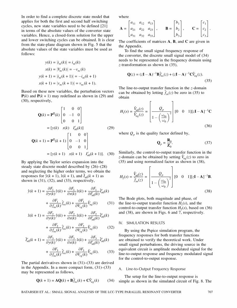
375 :The coefficients of matrices A, B, and C are given inthe Appendix.To find the small signal frequency response of
the converter, the discrete small signal model of (34)needs to be represented in the frequency domain usingz-transformation as shown in (35),
Q(z) = (zI¡A)¡1Bfns(z) + (zI¡A)¡1CVng(z):(35)
The line-to-output transfer function in the z-domaincan be obtained by letting fsn(z) be zero in (35) toobtain
H1(s) =Vn0(z)
Vng(z)=
26664 Qp
1¡μ!0s!0
¶237775[0 0 1][zI¡A]¡1C
(36)
where Qp is the quality factor defined by,
Qp =R0Z0: (37)
Similarly, the control-to-output transfer function in thez-domain can be obtained by setting Vng(z) to zero in(35) and using normalized factor as shown in (38),
H2(s) =Vn0(z)
fsn(z)=
26664 Qp
1¡μ!0s!0
¶237775[0 0 1][zI¡A]¡1B:
(38)
The Bode plots, both magnitude and phase, ofthe line-to-output transfer function H1(s), and thecontrol-to-output transfer function H2(s), based on (36)and (38), are shown in Figs. 6 and 7, respectively.
IV. SIMULATION RESULTS
By using the Pspice simulation program, thefrequency responses for both transfer functionsare obtained to verify the theoretical work. Undersmall signal perturbations, the driving source in theequivalent circuit is amplitude modulated signal for theline-to-output response and frequency modulated signalfor the control-to-output response.
A. Line-to-Output Frequency Response
The setup for the line-to-output response issimple as shown in the simulated circuit of Fig. 8. The
BATARSEH ET AL.: SMALL SIGNAL ANALYSIS OF THE LCC-TYPE PARALLEL RESONANT CONVERTER 707

Fig. 6. Line-to-output frequency response. Theoretical results: solid line. Simulated results: broken line.
Fig. 7. Control-to-output frequency response. Theoretical results: solid line. Simulated results: broken line.
converter values are based on a design example for thefollowing values:
DC input voltage Vg = 10 V
Load current I0 = 5 A
Output voltage V0 = 15 V
Switching frequency fs = 100 kHz
Capacitor ratio Cp=Cs = 0:5
The converter component values are given as follows:
R0 = 3 −, L0 = 20 mH, L= 3:1252 ¹H,
Cp = 1:63 ¹, Cs = 1:63 ¹:
Source vA(t) is a 50% duty ratio square wave signalwith switching frequency of 100 kHz and amplitudesof §10 V. Source vF(t) generates the small signal
Fig. 8. Simulated circuit for line-to-output response.
perturbation with dc offset of 10 V (vF(t) = 10+sin(2¼fmt)), where fm is the small signal frequencybetween 10 Hz and 100 kHz. Source vE(t) is adependent signal which generates the square wave
708 IEEE TRANSACTIONS ON AEROSPACE AND ELECTRONIC SYSTEMS VOL. 32, NO. 2 APRIL 1996

Fig. 9. Simulated waveforms for 4 kHz perturbation signal forFig. 8. v(1): input (reference) voltage. v(5,3): output voltage.
Fig. 10. Simulated circuit for control-to-output response.
amplitude modulated signal with peak amplitudeof 10 V (vE(t) = 0:1vF(t)vA(t)). Fig. 9 shows theoutput response at perturbation signal of 4 kHz. Thesimulation results for the line-to-output frequencyresponse is shown in Fig. 6.
B. Control-to-Output Frequency Response
The simulated circuit for the control-to-outputresponse is shown in Fig. 10 with the same convertercomponents given in Fig. 9. In Fig. 10, the sourcevA(t) is frequency modulated signal, vF(t) is used as asmall signal reference source, and vE(t) is a dependentsource that generates the square wave single frequencymodulated signal. These sources are defined as follows.Source A: vA(t) = A1 sin[2¼fct+B sin(2¼fmt) where
A1 500 V,
fc 100 kHz (switching frequency),
fm Small signal frequency (10 Hz< fm <
100 kHz),
¢f 1:0%fc (switching frequency deviation),
B Modulation index (B =¢f=fm):
Source F: vF(t) = A2 cos(2¼fmt) where
A2 0:05 V (small signal amplitude),
fm Perturbation frequency (10 Hz< fm <
100 kHz):
Fig. 11. Simulated waveforms for 10 kHz perturbation signal forFig. 10. v(6): input (reference) voltage. v(5,3): output voltage.
Source E: vE(t) = Vz(t) where the zener voltages ofthe diodes are set to 10 V.Fig. 11 shows the output response due to the
control frequency perturbation at 10 kHz. Thesimulation results are also plotted in Fig. 7. Thesesresults show that the frequency responses from boththe theory and simulation are in good agreement,especially at low frequencies.
V. CONCLUSION
The small signal analysis for the LCC-PRCoperating in the CCM has been presented. Theclosed form solution of the small signal response canbe obtained from the state-plane diagram with theapplication of Taylor series expansion. Two relatedtransfer functions under line and control perturbationswere derived: line-to-output and control-to-outputtransfer functions. Using z-transformation, frequencyresponses for these two transfer functions werederived. Finally, simulated results for the magnitudeand phase responses of the transfer functions werereported and compared to verify the theoreticalapproach. It was shown that the simulated resultsare in good agreement with the theoretical results,especially at low frequencies. Since accurate knowledgeof the transfer function is more critical close to thecross-over frequency (i.e., for magnitudes close to one),the relatively high error at high frequencies poses noproblems.
APPENDIX
A. Derivation of Partial Derivatives for (32)
The coefficients of matrices A, B, and C associatedwith y(k+1):
@F1@y(k)
= a11 =¡·@Vnm2@y(k)
sinμ4 +Vnm2 cosμ4
£μ@μ2@y(k)
¡ @μ1@y(k)
+@μ3@y(k)
¶¸
BATARSEH ET AL.: SMALL SIGNAL ANALYSIS OF THE LCC-TYPE PARALLEL RESONANT CONVERTER 709

@F1@x(k)
= a12 =¡·@Vnm2@x(k)
sinμ4 +Vnm2 cosμ4
£μ@μ2@x(k)
¡ @μ1@x(k)
+@μ3@x(k)
¶¸@F1@In0(k)
= a13 =¡·1+
@Vnm2@I 0n0(k)
sinμ4 +Vnm2 cosμ4
£μ
@μ2@I0n0(k)
¡ @μ1@I 0n0(k)
+@μ3@I0n0(k)
¶¸@F1@fns(k)
= b1 =¡Vnm2 cosμ4μ¼
F2ns
¶@F1
@Vng(k)= c1 =¡
"@Vnm2@Vng(k)
sinμ4 +Vnm2 cosμ4
£μ
@μ2@Vng(k)
¡ @μ1@Vng(k)
+@μ3
@Vng(k)
¶¸:
B. Derivation of Partial Derivatives for (33)
The coefficients of matrices A, B, and C associatedwith x(k+1):
@F2@y(k)
= a21 =@Vnm2@y(k)
cosμ4
¡Vnm2 sinμ4³@μ2@y(k)
¡ @μ1@y(k)
+@μ3@y(k)
´@F2@x(k)
= a22 =@Vnm2@x(k)
cosμ4
¡Vnm2 sinμ4³@μ2@x(k)
¡ @μ1@x(k)
+@μ3@x(k)
´@F2@In0(k)
= a23 =@Vnm2@I0n0(k)
cosμ4
¡Vnm2 sinμ4μ
@μ2@I0n0(k)
¡ @μ1@I0n0(k)
+@μ3
@I0n0(k)
¶@F2@fns(k)
= b2 =¡Vnm2 sinμ4μ¼
F2ns
¶@F2
@Vng(k)= c2 = 1+
@Vnm2@Vng(k)
cosμ4
¡Vnm2 sinμ4μ
@μ2@Vng(k)
¡ @μ1@Vng(k)
+@μ3
@Vng(k)
¶:
C. Derivation of Partial Derivatives for (34)
The coefficients of matrices A, B, and C associatedwith I0n0(k+1):
@F3@y(k)
= a31 =¡2Z0!0L0
"1¡μ!0s!0
¶2#2³@μ2@y(k)
¡ @μ1@y(k)
´
@F3@x(k)
= a32 =¡2Z0!0L0
"1¡μ!0s!0
¶2#2³@μ2@x(k)
¡ @μ1@x(k)
´
+2L1L0
"1¡μ!0s!0
¶2#21I0n0(k)
@F3@I0n0(k)
= a33 = 1¡2Z0!0L0
"1¡μ!0s!0
¶2#2μ@μ2
@I0n0(k)
¡ @μ1@I0n0(k)
¶
¡ 2L1L0
"1¡μ!0s!0
¶2#2x(k)
I20n0(k)
¡ ¼R0!0L0Fsn
@F3@Vng(k)
= b3 =¡Z0!0L0
"1¡μ!0s!0
¶2#2¼
F2ns+¼R0I
0n0
!0L0F2ns
@F3@Vng(k)
= c3 =¡Z0!0L0
"1¡μ!0s!0
¶2#2μ@μ2
@Vng(k)¡ @μ1@Vng(k)
¶:
D. Other Parameters
Below are other parameters relevant for thederivation of the coefficients of (32) and (33).1) Partial Derivatives for Paramter Vnm2:
@Vnm2@y(k)
=y(k)+ I 0n0(k)
Vnm2
@Vnm2@x(k)
=x(k)¡ 1Vnm2
@Vnm2@I0n0(k)
=y(k)+ I 0n0(k)
Vnm2
@Vnm2@Vng(k)
=x(k)+1Vnm2
:
2) Partial Derivatives for Parameter μ1:
@μ1@y(k)
=
μx(k)I0n0(k)
+ I 0n0(k)¶Hxy(k)+ I 0n0(k))
V2nm1
sV2nm1¡
μx(k)I0n0(k)
+ I0n0(k)¶2
@μ1@x(k)
=
μx(k)I0n0(k)
+ I 0n0(k)¶(x(k)+1)I0n0(k)¡V2nm1
V2nm1I0n0(k)
sV2nm1¡
μx(k)I 0n0(k)
+ I0n0(k)¶2
@μ1@Vng(k)
=
μx(k)I0n0(k)
+ I 0n0(k)¶(x(k)+1)
V2nm1
sV2nm1¡
μx(k)I 0n0(k)
+ I0n0(k)¶2
710 IEEE TRANSACTIONS ON AEROSPACE AND ELECTRONIC SYSTEMS VOL. 32, NO. 2 APRIL 1996

@μ1@I0n0(k)
=
μx(k)I0n0(k)
+ I0n0(k)¶·μ
y(k) +x2(k)I30n0(k)
¶¸V2nm1
sV2nm1¡
μx(k)I0n0(k)
+ I 0n0(k)¶2
¡
μ1¡ x(k)
I20n0(k)
¶μV2nm1¡
μx(k)I20n0(k)
¶¶V2nm1
sV2nm1¡
μx(k)I0n0(k)
+ I0n0(k)¶2 :
3) Partial Derivatives for Parameter μ2:
@μ2@y(k)
=x(k)+1V2nm1
@μ2@x(k)
=¡y(k)¡ I 0n0(k)
V2nm1
@μ2@y(k)
=x(k)+1V2nm1
@μ2@x(k)
=¡y(k)¡ I 0n0(k)
V2nm1:
4) Partial Derivatives for Parameter μ3:
@μ3@y(k)
=
μx(k)I0n0(k)
¡ I0n0(k)¶(y(k) + I0n0(k))
V2nm2
sV2nm1¡
μx(k)I0n0(k)
+ I0n0(k)
¶2
@μ3@x(k)
=μx(k)I0n0(k)
¡ I0n0(k)¶(x(k) +1)I0n0(k)¡V2nm1 +2x(k) +2I20n0(k)
V2nm2I
0n0(k)
sV2nm1¡
μx(k)I0n0(k)
+ I0n0(k)
¶2
@μ3@I0n0(k)
=
μx(k)
I20n0(k)
+1
¶"V2nm1¡
μx(k)I0n0(k)
+ I0n0(k)
¶2#
V2nm2
sV2nm1¡
μx(k)I0n0(k)
+ I0n0(k)
¶2
+
μx(k)I0n0(k)
¡ I0n0(k)¶μ
y(k) +x2(k)
I30n0(k)
¶V2nm2
sV2nm1¡
μx(k)I0n0(k)
+ I0n0(k)
¶2
@μ3@Vng(k)
=
μx(k)I0n0(k)
¡ I0n0(k)¶(x(k)+ 1)
V2nm2
sV2nm1¡
μx(k)I0n0(k)
+ I0n0(k)
¶2:
REFERENCES
[1] Lau, B. Y. (1988)Small-signal input-to-output frequency response ofswitching converters.In IEEE Power Electronics Specialists Conference Record, 2(Apr. 1988), 1355—1363.
[2] Brown, A. R., and Middlebrook, R. D. (1981)Sampled data modeling of switching regulators.In IEEE Power Electronics Specialists Conference Record,1981, 349—369.
[3] Redl, R., Molnar, B., and Sokal, N. O. (1984)Small-signal dynamic analysis of regulated class-E dc/dcconverters.In IEEE Power Electronics Specialists Conference Record,1984, 62—71.
[4] Middlebrook, R. D., and Cuk, S. (1976)A general unified approach to modeling switchingconverter power stages.In IEEE Power Electronics Specialists Conference Record,1976, 18—34.
[5] King, R. J., and Stuart, T. A. (1985)Small-signal model for the series resonant converter.IEEE Transactions on Aerospace and Electronic Systems,AES-21, 3 (May 1985), 301—319.
[6] Panov, Y. V., and Lee, F. C. (1994)A novel control evaluation technique for resonantconverters.In IEEE Power Electronics Specialists Conference Record,1994, 301—308.
[7] Verghese, G. C., Elbuluk, M. E., and Kassakian, J. G. (1986)A general approach to sampled-data modeling for powerelectronic circuits.IEEE Transactions on Power Electronics, PE-1 (Apr. 1986),76—89.
[8] Vlatkovic, V., Sabate, J., Ridley, R., Lee, F. C., and Cho, B.(1992)Small-signal analysis of the phase-shifted PWM converter.IEEE Transactions on Power Electronics, 7, 1 (Jan. 1992),128—135.
[9] Vorperian, V., Tymerski, R., and Lee, F. C. (1985)Equivalent circuit for resonant and PWM switches.IEEE Transactions on Power Electronics, PE-4, 2 (Apr.1985), 205—214.
[10] Middlebrook, R. D., and Cuk, S. (1983)Advances in Switched-Mode Power Conversion, Vols. 1and 2.Teslaco: Pasadena, CA, 1983.
[11] Sanders, S. R., Noworolski, J. M., Liu, X. Z., and Verghese,G. C. (1990)Generalized averaging method for power conversioncircuits.In IEEE Power Electronics Specialists Conference Record,June 1990, 333—340.
[12] Vorperian, V. (1990)Simplified analysis of PWM converters using the model ofthe PWM switch: Parts I and II.IEEE Transactions on Aerospace and Electronic Systems,26, 3 (1990), 490—505.
[13] Vorperian, V., and Cuk, S. (1983)Small signal analysis of resonant converters.In IEEE Power Electronics Specialists Conference Record,Albuquerque, NM, June 6—9, 1983, 269—283.
[14] Witulski, A. R., and Erickson, R. W. (1987)Small signal ac equivalent circuit modelling of the seriesresonant converter.In IEEE Power Electronics Specialists Conference Record,1987, 693—704.
BATARSEH ET AL.: SMALL SIGNAL ANALYSIS OF THE LCC-TYPE PARALLEL RESONANT CONVERTER 711

[15] Siri, K. (1991)Small signal analysis of resonant converters and controlapproaches for parallel-connected converter systems.Ph.D. dissertation, University of Illinois at Chicago,Department of Electrical Engineering and ComputerScience, Chicago, IL, July 24, 1991.
[16] Siri, K., Lee, C. Q., and Fang, S. J. (1990)Frequency response of resonant converters.In Proceedings of IEEE Industrial Electronics Conference,Pacific Grove, CA, Nov. 1990, Vol. II, 944—949.
[17] Elbuluk, M. E., Verghese, G. C., and Kassakian, J. G. (1988)Sampled-data modeling and digital control of resonantconverters.IEEE Transactions on Power Electronics, 3 (July 1988),344—354.
[18] Vorperian, V. (1989)Approximate small-signal analysis of the series and theparallel resonant converters.IEEE Transactions on Power Electronics, 4 (Jan. 1989),15—24.
[19] Siri, K., Fang, S. J., and Lee, C. Q. (1991)State-plane approach to frequency response of resonantconverters.IEE Proceedings, Pt.-G (Electronics Circuit and Systems),138, 5 (Oct. 1991), 557—563.
[20] Witulski, A. R., and Erickson, R. W. (1987)Small signal ac equivalent circuit modeling of the seriesresonant converter.In IEEE Power Electronics Specialists Conference Record,1987, 693—704.
[21] Batarseh, I., and Siri, K. (1993)Generalized approach to the small signal modeling ofdc-to-dc resonant converters.IEEE Transactions on Aerospace and Electronic Systems,29, 3 (July 1993), 894—909.
[22] Siri, K., Batarseh, I., and Lee, C. Q. (1993)Frequency response for the conventional parallel resonantconverter based on the state-plane diagram.IEEE Transactions on Circuits and Systems, 40, 1 (Jan.1993), 33—42.
[23] Yang, E. X., and Lee, F. C. (1992)Small signal modeling of LLC-type series resonantconverter.HFPC’92, San Diego, CA, May 3—7, 1992, 186—197.
[24] Yang, E. X., Lee, F. C., and Jovanovic, M. (1992)Small signal modeling of LCC-type parallel resonantconverter.In IEEE Power Electronics Specialists Conference Record,1992, 941—948.
[25] Steigerwald, R. L. (1988)A comparison of half-bridge resonant convertertopologies.IEEE Transactions on Power Electronics, 3 (Apr. 1988),174—182.
[26] Bhat, A. K. S. (1993)Analysis and design of a series-parallel resonant converter.IEEE Transactions on Power Electronics, 8, 1 (Jan. 1993),1—11.
[27] Batarseh, I., Liu, R., Lee, C. Q., and Upadhyay, A. K. (1990)Theoretical and experimental studies of the LCC-typeparallel resonant converter.IEEE Transactions on Power Electronics, 5, 2 (Apr. 1990),140—150.
[28] Batarseh, I., and Lee, C. Q. (1989)High frequency high order parallel resonant converter.IEEE Transactions on Power Electronics, 36, 4 (Nov. 1989),485—495.
[29] Batarseh, I. (1990)Analysis and design of high order parallel resonantconverters.Ph.D. dissertation, University of Illinois at Chicago, June1990.
[30] Oruganti, R., and Lee, F. C. (1985)Resonant power processing: Part I–state-plane analysis.IEEE Transactions on Industry Applications, (Nov. 1985),1443—1460.
[31] Oruganti, R., and Lee, F. C. (1985)Resonant power processing: Part II–method of control.IEEE Transactions on Industry Applications, (Nov. 1985),1461—1471.
712 IEEE TRANSACTIONS ON AEROSPACE AND ELECTRONIC SYSTEMS VOL. 32, NO. 2 APRIL 1996

Issa Batarseh (S’83–M’91–SM’92) was born in Jordan on January 29, 1961. Hereceived his B.S., M.S., and Ph.D. from the University of Illinois at Chicago in1983, 1985, and 1990, respectively, all in electrical engineering.He was a visiting Assistant Professor in the Electrical Engineering Department
at Purdue University Calumet, from 1989 to 1990. In August 1991, he joined theDepartment of Electrical and Computer Engineering at the University of CentralFlorida in Orlando, as an Assistant Professor. He is currently engaged in researchin the area of power electronics. His research interests include PWM and highfrequency resonant converters, power factor correction circuits, and small signalmodeling of dc-to-dc resonant converters.Dr. Batarseh is a member of Tau Beta Pi and Eta Kappa Nu. Presently serving
as Chairman of the IEEE-PE/IAS/PEL Orlando Chapter. From 1991—1993 heserved as advisor to Eta Kappa Nu at the University of Central Florida. He isa registered Professional Engineer in Florida. He has served on the programcommittees of IEEE APEC, PESC, IECON and IAS.
Mario Sznaier (M’XX) received the Ingeniero Electronico and Ingeniero enSistemas de Computacion degrees from the Universidad de la Republica, Uruguayin 1983 and 1984, respectively, and the MSEE and Ph.D. degrees from theUniversity of Washington, Seattle, in 1986 and 1989, respectively.He spent 1990 as a Research Fellow in Electrical Engineering at California
Institute of Technology. From 1991 to 1993 he was an Assistant Professor ofElectrical Engineering at the University of Central Florida. In 1993 he joined theDepartment of Electrical Engineering at Pennsylvania State University, where heis currently an Assistant Professor. His research interest include multiobjectiverobust control, l1 and H1 control theory, applications of robust control to powerelectronics, and legged locomotion.In 1992 Dr. Sznaier was awarded a National Science Foundation Research
Initiation Award for his research on robust control of systems under mixedtime/frequency domain performance specifications. He is a member of SIAM, TauBeta Pi, and Eta Kappa Nu. From 1992 to 1993 he served as the faculty advisorto the IEEE Student Branch at UCF, and from 1993 he has been a co-advisor toPenn State’s IEEE Student Branch. He served in the program committee of the1994 IEEE CDC and is a member of the Control Systems Society ConferenceEditorial Board.
C. Magalemos photograph and biography not available.
BATARSEH ET AL.: SMALL SIGNAL ANALYSIS OF THE LCC-TYPE PARALLEL RESONANT CONVERTER 713