smart systems integration - advancing 3d system...
TRANSCRIPT

maris TechConmaris TechCon - Technology and R&D Consulting
Dr. Markus [email protected]
www.maristechcon.com
Smart Systems Integration -Advancing 3D system integration and
miniaturization
Markus Riester
March 25, 2009
MIT Europe Conference 2009March 25/26, 2009
26. March 2009, 2, Markus Riester
Agenda
• What is Smart Systems Integration, what is a Smart Integrated System?
– Definition, Attributes, Markets & Applications
– What does a Smart Integrated System do?
• How do you build Smart Integrated Systems?
– Technologies for building Smart Systems

26. March 2009, 3, Markus Riester
What is Smart Systems Integration ? What is a Smart Integrated System ?
26. March 2009, 4, Markus Riester
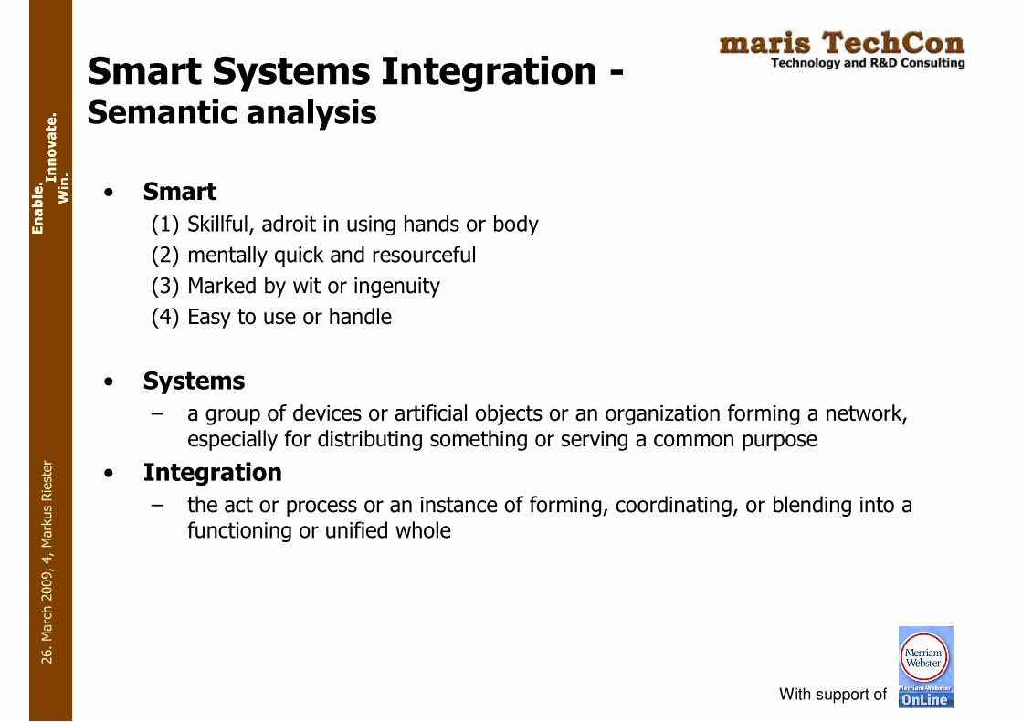
Smart Systems Integration -Semantic analysis
• Smart
(1) Skillful, adroit in using hands or body
(2) mentally quick and resourceful
(3) Marked by wit or ingenuity
(4) Easy to use or handle
• Systems
– a group of devices or artificial objects or an organization forming a network, especially for distributing something or serving a common purpose
• Integration
– the act or process or an instance of forming, coordinating, or blending into a functioning or unified whole
With support of

26. March 2009, 5, Markus Riester
Smart Systems Integration
• search: first 30 entries
Smart System Integration Annual Conference
European Technology Platform

26. March 2009, 6, Markus Riester
Smart Systems –Bridging the gap
SoftwareComponents
Products
Smart Systems
autonomous
efficient
robust
usable
Materials Tools
Smart Systems in the Value Chain
Schymanietz, SSI09, Brussels, March 10/11, 2009

26. March 2009, 7, Markus Riester
Attributes of Smart Integrated Systems
• Integrated systems, which are able to sense and diagnose a situation and to describe it
• Mutually address and identify each other
• Are predictive and are able to decide and help to decide
• Operate in a discreet, ubiquitous and quasi invisible manner
• Utilise properties of materials, components or processes in an innovative way to achieve more performance and new functionalities
• Are able to interface, interact and communicate with the environment and with other Smart Systems
• Are able to act, perform multiple tasks and assist the user

26. March 2009, 11, Markus Riester
Intelligent and cognitivesystems
Smart Systems Integration• mechanistic, technology
driven view on integration
and miniaturization
Intelligent and cognitive systems(i.e. EU FP7 ICT-2007.8.5 programme) go beyond SSI and use
technology to create evolutionary self-optimizing systems
Short/Mid term Long term

26. March 2009, 12, Markus Riester
The evolution of Smart Systems
2nd generation
Smart Systems
3rd generationSmart Systems
Integrated, miniaturised systems
with advanced functionality.
Predictive & reactive systems matching harsh environments andequipped with advanced energy
management capabilities.
Self aware, autonomous systemsinterfacing physical w/ virtual world,
adaptive to environment, ubiquitously connected, with cognitive abilities
1st generationSmart Systems
Functions Complexity
26. March 2009, 13, Markus Riester
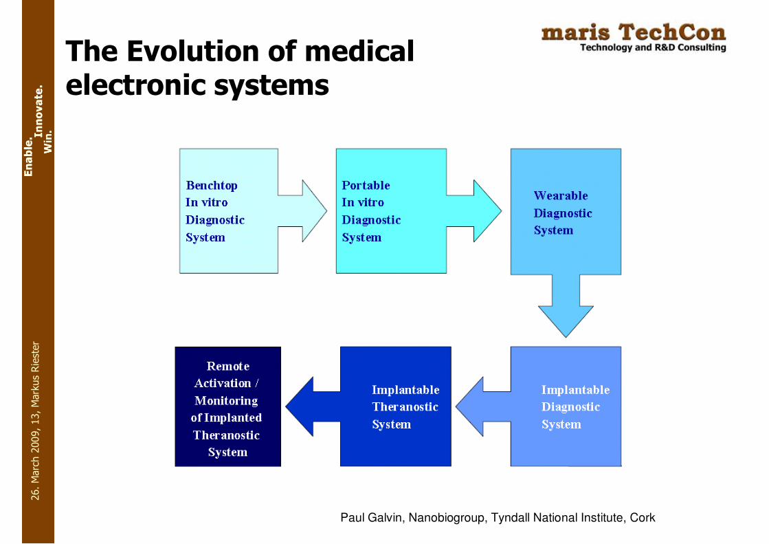
The Evolution of medicalelectronic systems
Paul Galvin, Nanobiogroup, Tyndall National Institute, Cork
26. March 2009, 14, Markus Riester
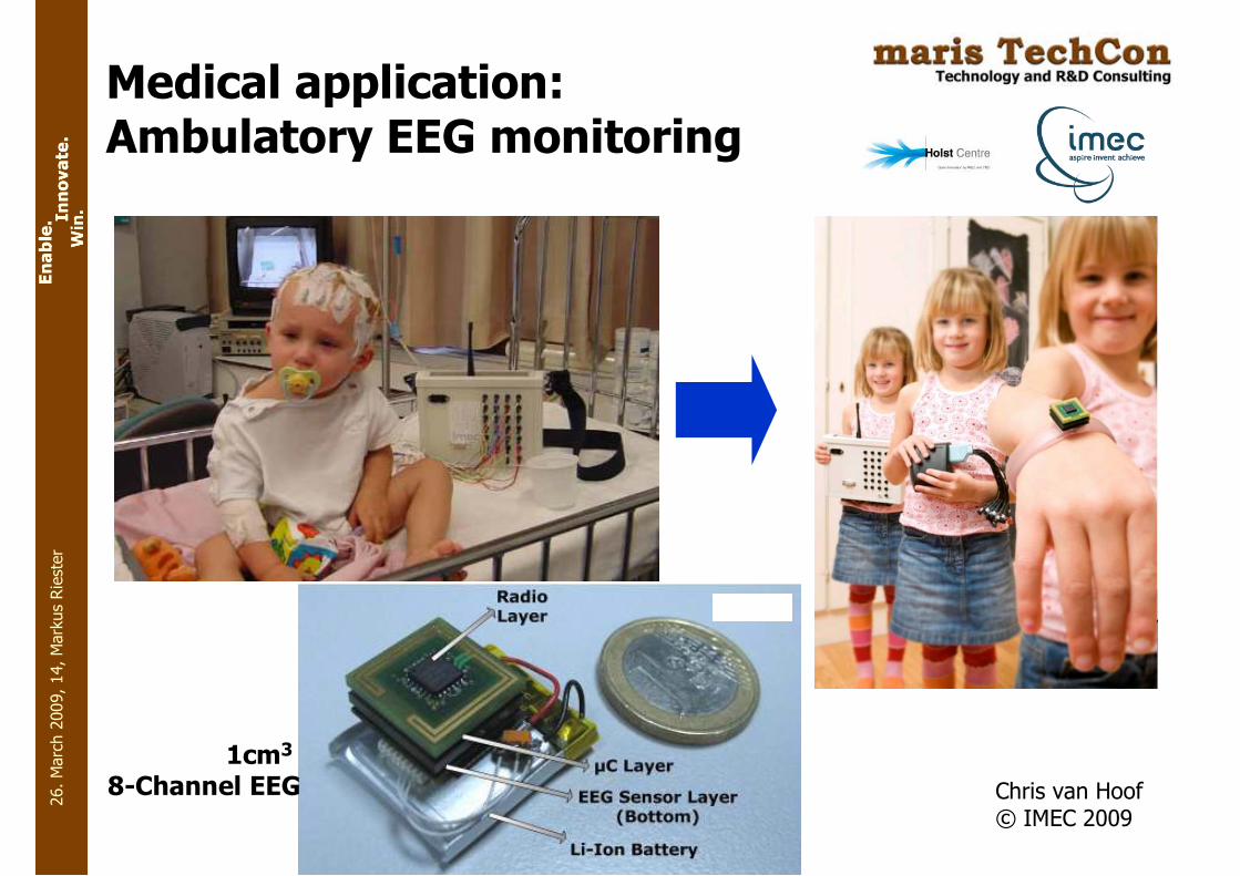
Medical application: Ambulatory EEG monitoring
Chris van Hoof© IMEC 2009
1cm3
8-Channel EEG
26. March 2009, 15, Markus Riester
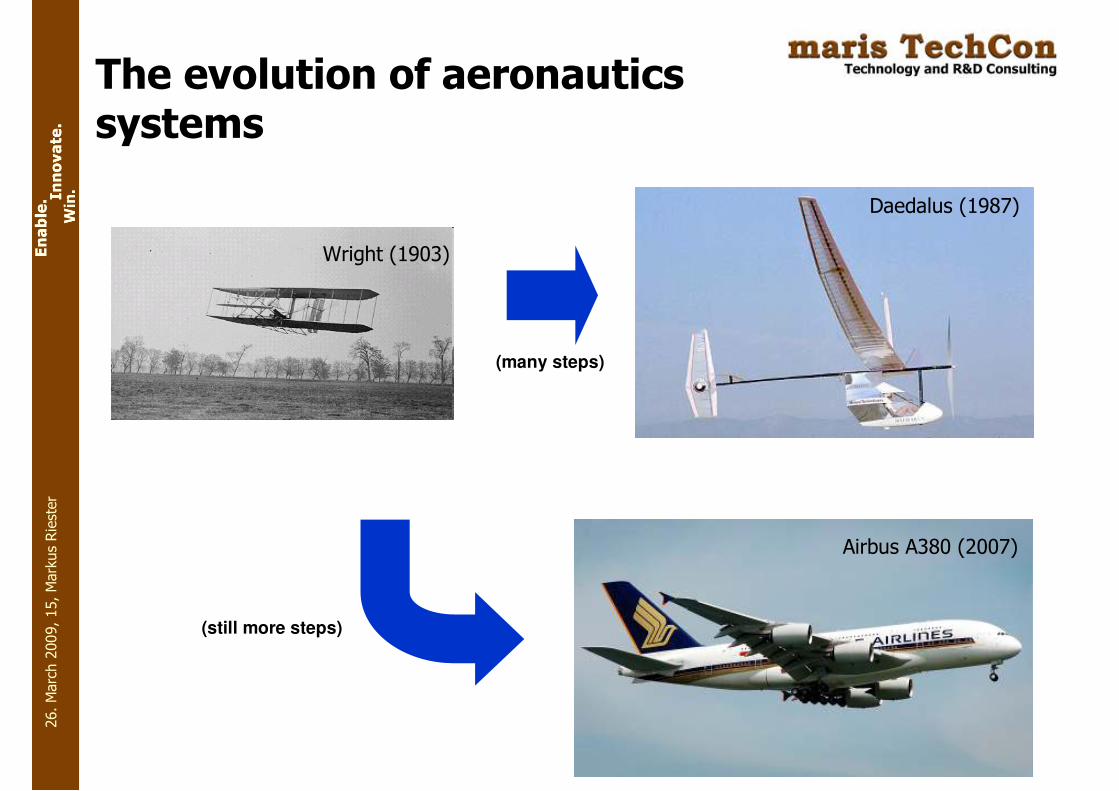
The evolution of aeronauticssystems
Airbus A380 (2007)
Wright (1903)
(many steps)
(still more steps)
Daedalus (1987)

26. March 2009, 16, Markus Riester
Application of AbandonedSensor
Antenna 1
An
tenn
a 2
An
ten
na
3
diagram at time Ti
diagram at time Ti + 1
© 3D Plus

26. March 2009, 20, Markus Riester
Application of Tire-Pressure Monitoring Systems (TPMS)
Today’s rim mounted TPMS: ~60cm³
Future self-sufficient tire mounted TPMS: <1cm³

26. March 2009, 24, Markus Riester
Main challenges for Microsystems and smart miniaturised systems
1. Multiple research fields to combine
– Mechanics, electronics, fluidics, biology, magnetism, photonics
2. Multiple materials need to work side by side
– Semiconductor, ceramic, glass, organic
3. Multiple functions to integrate
– Sensing, processing, logic, memory, communication, actors
4. Multiple integration options towards Heterogeneous Integration
– Monolithic, hybrid, multichip, …
Budapest ICT Proposers’ Day 2009 – 22-Jan-09 – Griet van Caenegem

26. March 2009, 25, Markus Riester
Smart Dust
Warneke, Last, Liebowitz, Pister (2001)Stanislaw Lem (1964)
University of California, Berkeley: Smart Dust (Motes), Tiny OS, Picoradio
IZM: eGRAIN, AVM
IMEC: System in a Cube e-Grain
NMRC, Irland: I-Seed
VTT Electronics: SoapBox
ETH Zurich: Smart Its
26. March 2009, 26, Markus Riester
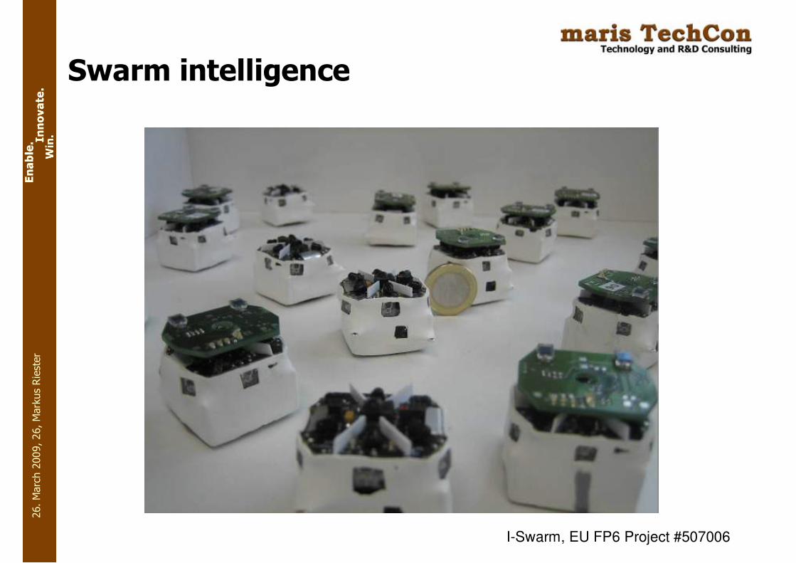
Swarm intelligence
I-Swarm, EU FP6 Project #507006

26. March 2009, 27, Markus Riester
Who needs smart integrated systems?
26. March 2009, 28, Markus Riester
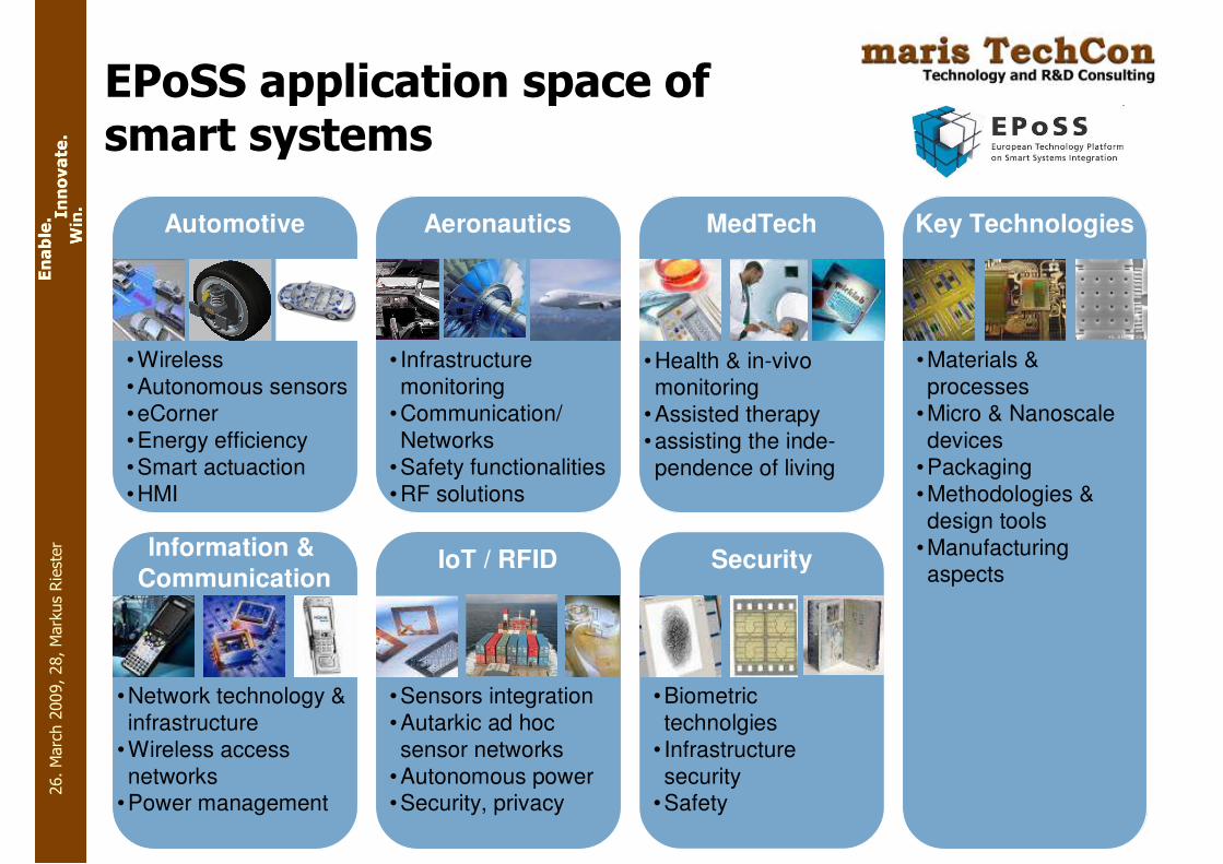
EPoSS application space of smart systems
Automotive Aeronautics MedTech
Information &
CommunicationIoT / RFID Security
• Infrastructure
monitoring
•Communication/
Networks
•Safety functionalities
•RF solutions
•Sensors integration
•Autarkic ad hoc
sensor networks
•Autonomous power•Security, privacy
•Health & in-vivo monitoring
•Assisted therapy
•assisting the inde-
pendence of living
•Network technology &
infrastructure
•Wireless access
networks•Power management
•Wireless
•Autonomous sensors
•eCorner
•Energy efficiency
•Smart actuaction
•HMI
Key Technologies
•Materials &
processes
•Micro & Nanoscale
devices
•Packaging
•Methodologies &
design tools
•Manufacturing aspects
•Biometric
technolgies
• Infrastructure
security•Safety

26. March 2009, 29, Markus Riester
Applications of Smart Systems
Source: EPoSS Strategic Research Agenda, 03/09

26. March 2009, 30, Markus Riester
European NanoelectronicsInitiative Advisory Council
• The technology behind the curtain of Smart Systems
Application Environments
System Integration
“Heterogenous Integration”
More Moore
Nanoelectronics
↑
Microelectronics
More than Moore
(Nano) Electronics +
Sensors & Actuators(e.g. Opto-/ Biotechnology)
Requirements
Technology
SoCMicro
Systems
Macro
Systems

26. March 2009, 31, Markus Riester
How are Smart Systems integrated?

26. March 2009, 32, Markus Riester
Electronics Value Chain

26. March 2009, 33, Markus Riester
Advancing 3D Integration & Miniaturization
Printed Circuit Board
Assembly
Packaging
Key Manufacturingtechnologies
Key Manufacturingtechnologies
Methodologies & design tools
Semiconductor
Test

26. March 2009, 34, Markus Riester
Advancing 3D Integration & Miniaturization
Optics & Photonics
RF
Energy
Surfaceengineering
Technology domains
Technology domains
Human machineInterfaces
Communicationnetworks
Printedelectronics
Logistics & Supply Chain
Materials & processes

26. March 2009, 35, Markus Riester
JISSO – the total packagingsolution
Jisso is Japanese and stands for
Total solution for Interconnecting, Assembling, Packaging, Mounting and
Integrating system design.
Supports and encourages
• standards development at an international level
• the development of technological roadmaps
• addressing environmental issues
• monitoring of market trends.Source: jisso.ipc.org
26. March 2009, 36, Markus Riester
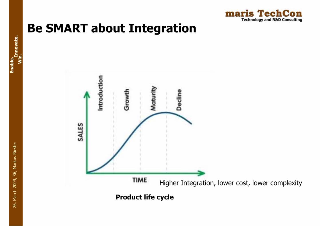
Be SMART about Integration
Product life cycle
Higher Integration, lower cost, lower complexity

26. March 2009, 37, Markus Riester
Advancement through higherintegration
Power 65Transceiver 86Total 151
Power 54Transceiver 49Total 104
Parts count
Parts count reduced by 1/3 on same area, with increased functionality.

26. March 2009, 38, Markus Riester
Semiconductor – More Moore

26. March 2009, 42, Markus Riester
Silicon integration vs. packaging
Source: IBM, Intel

26. March 2009, 43, Markus Riester
Pushing the limits of integration
High Density
Interconnect Board
High Density
Interconnect Board
3D Integration3D Integration Embedded ActivesEmbedded Actives
OpticalInterconnectsOpticalInterconnects
Integrated
Heat Sinks
Integrated
Heat Sinks
MEMS
Components
MEMS
Components
Integrated
RF Components
Integrated
RF ComponentsIntegratedPassivesIntegratedPassives
Power
Converter
Power
Converter

26. March 2009, 44, Markus Riester
Pushing the limits of packaging
Chip-on-Chip
Wire
bonding
Edge connection
Bus metal Bus silver
epoxy
Wafer Level Stacking
Rebuilt Wafer
to Rebuilt
wafer
Wafer to wafer
Thru-Polymer Via
« TPV »
Thru-Si Via
« TSV »
- Amkor- ASE- STATS
ChipPac- … - 3D Plus
- Irvine Sensors - VCI - IBM- INTEL- ST Micro- Micron- Toshiba- Tezzaron- Ziptronix- Samsung- …
- 3D Plus- Amkor
Amkor
Fraunhofer IZM
Fraunhofer ENAS
3D Plus

26. March 2009, 45, Markus Riester
Wirebonding
• Proven technology, widely implemented
Fraunhofer IZM

26. March 2009, 46, Markus Riester
3D Wafer-to-Wafer or Chip-to-Wafer Technologies
Through Si Via
(TSV) Technology
with CVD-Cu or
ECD Cu
72 µm
AR: 20 : 1
High aspect ratio
Si etching
Schematics of ICV (TSV) technology (FhG IZM Munich)

26. March 2009, 47, Markus Riester
Shrinking Silicon Packaging
~ 10 µm> 200 µm
sealing layercontact padseal glass
capping wafer

26. March 2009, 48, Markus Riester
PoP and WDoD
© 3D-Plus SA
Wireless Die-on-Die
Thickness per layer 100 µm
Rebuilt wafer with KGD
Package-on-Package
Thickness per die 100 µm
+ solder + package
26. March 2009, 50, Markus Riester
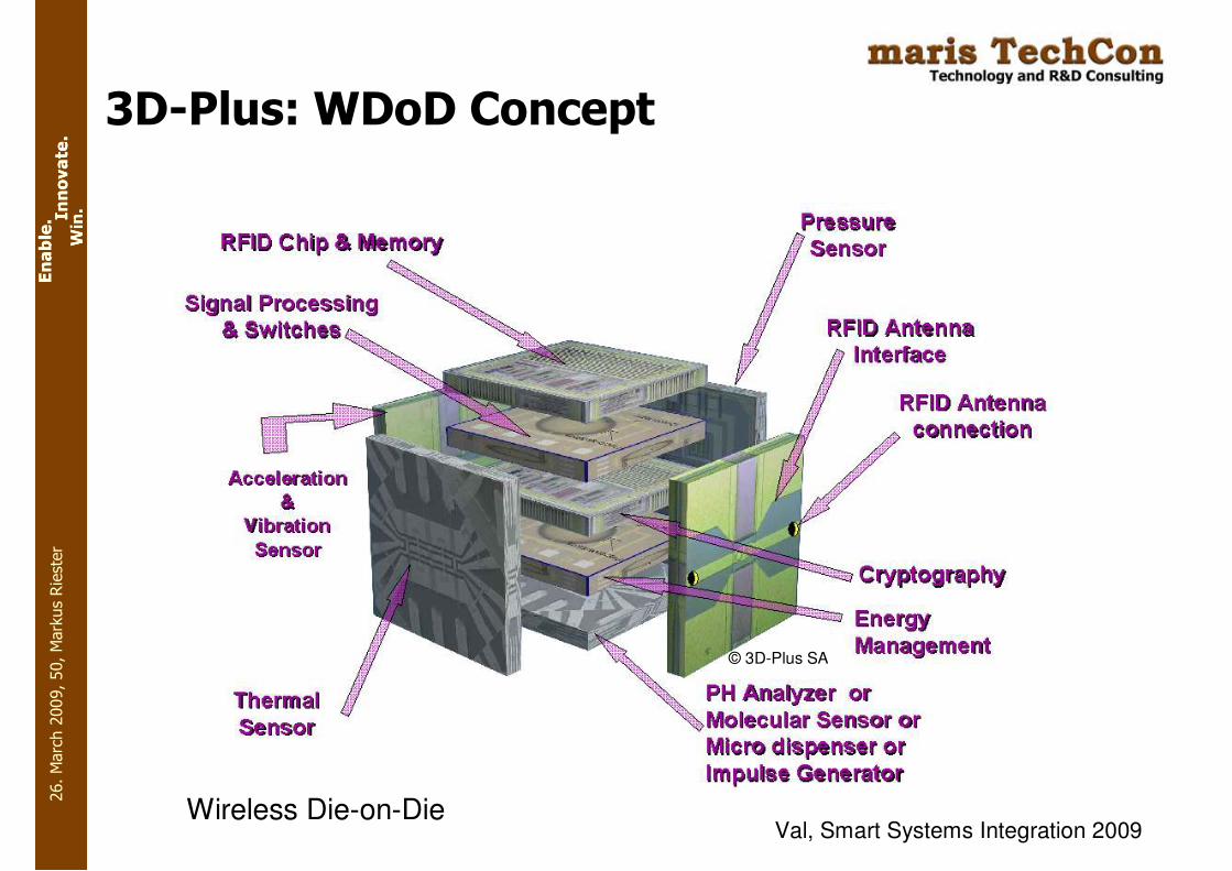
3D-Plus: WDoD Concept
Val, Smart Systems Integration 2009
© 3D-Plus SA
Wireless Die-on-Die

26. March 2009, 51, Markus Riester
Printed circuit boards
Legacy Circuit Boards
• Substrate on which components canbe assembled
• Wiring by wires or etched copper
State-of-the-art Circuit Boards
• Integrates functionality of hosting
components on and inside the board
• Substrate technology for smart systems
Historical Circuit Board, 1958 , © IBM Archives

26. March 2009, 52, Markus Riester
3D-PCBsMolded Interconnect devices
Motorcycle handle switch, Kromberg & Schubert
Duromer MID Package Schematic
26. March 2009, 53, Markus Riester
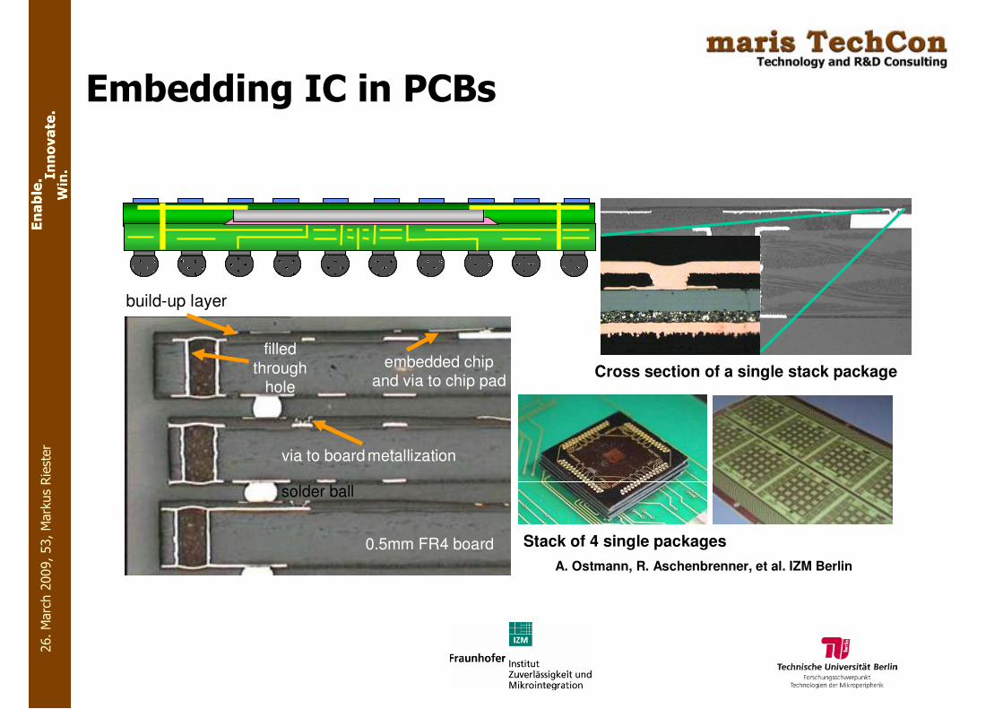
Embedding IC in PCBs
Cross section of a single stack package
via to board metallization
solder ball
filled through
hole
embedded chipand via to chip pad
build-up layer
0.5mm FR4 board Stack of 4 single packages
A. Ostmann, R. Aschenbrenner, et al. IZM Berlin
26. March 2009, 54, Markus Riester
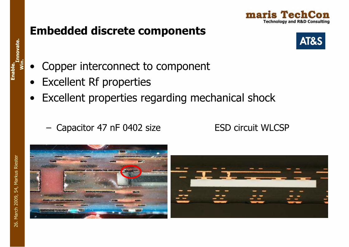
Embedded discrete components
• Copper interconnect to component
• Excellent Rf properties
• Excellent properties regarding mechanical shock
– Capacitor 47 nF 0402 size ESD circuit WLCSP
26. March 2009, 57, Markus Riester
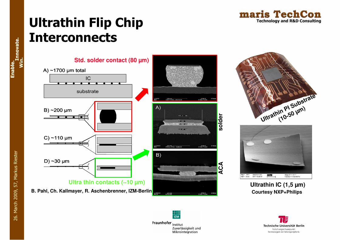
Ultrathin Flip Chip Interconnects
Ultra thin contacts (∼∼∼∼10 µm) Ultrathin IC (1,5 µm)Courtesy NXP+Philips
Ultrathin
PI Substra
te
(10-50 µm)
10 µm50 µm
650 µm
Std. solder contact (80 µm)
so
lde
rA
CA
B. Pahl, Ch. Kallmayer, R. Aschenbrenner, IZM-Berlin

26. March 2009, 58, Markus Riester
Folded Flex-PCB Integration

26. March 2009, 59, Markus Riester
Textile electronicsChris van Hoof© IMEC 2009

26. March 2009, 60, Markus Riester
Textile Electronics

26. March 2009, 61, Markus Riester
Printing Electronics
http://en.wikipedia.org/wiki/File:ComplementaryTechnologies.png

26. March 2009, 62, Markus Riester
Methodologies & Design Tools
• Specific Electronic Design Automation (EDA) tools forindividual technology domains exist
– Technical design decisions are supported in one technicaldomain
• No tool integrates knowledge accross domains!
• „Expert-system“ decision support for engineers desirabletaking into account all levels of integration!
�Room for R&D

26. March 2009, 63, Markus Riester
Example:Mobile Phone Electrical Design
Origin
Korea
Japan
1 2 3 4 5
#PCBs in phone

26. March 2009, 64, Markus Riester
Example:Mobile Phone Layout comparison
Japanese vs. Korean layout, single board designs

26. March 2009, 65, Markus Riester
What was not covered?
• Many other smart packaging methods and smart technology options
• Testability
• Manufacturability
• Reliability

26. March 2009, 66, Markus Riester
Reliability is critical
T
N
Nf
Reliability inexperiment
°C125
0-40
T
N
NfT
N
Nf
Reliability inexperiment
°C125
0-40
°C125
0-40
SimulationSimulation
ε ε ε ε cr
Deform
Creep
Strain
ε ε ε ε cr
Deform
Creep
Strain
Material
characterisation
Experiment
Material
characterisation
Experiment
Lifetime prediction
Failure analysis
T
N
T
N
T
N
Material Modells
verification
Lang, Fraunhofer IZM

26. March 2009, 67, Markus Riester
No matter what you do:Yield the Yield!
Process Yields
0%
10%
20%
30%
40%
50%
60%
70%
80%
90%
100%
0 1 2 3 4 5 6 7 8 9 10 11 12 13
Deviating processes
Overa
ll Y
ield
99,9
99,5
99
98,5
95
90
85
80
© maris TechCon

26. March 2009, 68, Markus Riester
Degrees of smartness
Technicalcapability
Wisdom/ Experience
Needs
Financialbackground

26. March 2009, 69, Markus Riester
Acknowledgements
• Stefan Rohringer, Infineon Technologies, AT
• Hannes Stahr, AT&S, AT
• Emil List, NTC Weiz, AT
• Klaus-Dieter Lang, Rolf Aschenbrenner, Fraunhofer IZM, DE
• Klaus Schymanietz, EADS, DE
• Sebastian Lange, VDI/VDE-IT, DE
• Chris van Hoof, IMEC, BE

26. March 2009, 70, Markus Riester
Thank you for your kind attention