smartphone acoustic impedance sensing based on …
TRANSCRIPT
SMARTPHONE ACOUSTIC IMPEDANCE SENSING
BASED ON
ADDITIVE SUM MIXING TECHNIQUE
BY
YUKUN REN
THESIS
Submitted in partial fulfillment of the requirements
for the degree of Master of Science in Electrical and Computer Engineering
in the Graduate College of the
University of Illinois at Urbana-Champaign, 2015
Urbana, Illinois
Advisor:
Associate Professor Logan Liu
ii
ABSTRACT
We have developed a method to perform impedance measurement using general purpose
smartphones that will not require the presence of external power source. The need for
battery-less impedance sensing methods is greatly demanded given recent years’
advancements in impedance based sensing technologies, such as impedance tomography,
which will enable patients to perform medical tests such as breast cancer self-detection
using only a smartphone.
The work discussed in this thesis is an early prototype of the impedance sensing method
done using MATLAB simulation of both hardware and algorithm for impedance sensing.
The battery-less acoustic impedance sensing technique is a combination of both hardware
circuit design as well as control software algorithm. The circuit hardware technology is
based on the additive summing mixer technology that is widely used in professional
audio production mixing consoles. The results presented in this thesis can be accurate to
within 0.1% of target device characteristics in simulation as far as tested.
Although not discussed in this work, in our early physical hardware prototypes, the
measurement based on the method discussed in this thesis has achieved accuracy within
10% of the target value with all the noise and parameter approximations.

iii
ACKNOWLEDGEMENTS
I would like to deliver my sincere gratitude to my master’s adviser, Professor Gang
Logan Liu, for providing me with the opportunity to pursue my master’s degree in UIUC.
In addition, I would love to acknowledge my fellow group members in the Liu
Nanobionics Lab as well as the staff members working in the ECE Electronics Service
shop for their patience and generous guidance.
Finally, I thank my family for all the love and patience along the way.

iv
TABLE OF CONTENTS
Chapter 1: Introduction ...................................................................................................... 1
1.1 Impedance Measurement History and Motivation .............................................. 1
1.2 Impedance Measurement Techniques ................................................................. 3
1.3 Commercial Network Analyzer IC: AD5933 ..................................................... 5
1.4 Stereo Soundcard RLC Measurement ................................................................. 7
1.5 Acoustic Summing Mixer-based Impedance Sensing ........................................ 8
Chapter 2: The Analog Mixer ............................................................................................ 9
2.1 Multiplicative Diode Mixer.................................................................................... 10
2.2 Additive Summing Mixer ...................................................................................... 11
2.3 Mathematical Model Simulation ............................................................................ 12
2.4 Phase Delayed Summing Mixer ............................................................................. 17
Chapter 3: Smartphone Audio Performance Characterizations ....................................... 18
3.1 Output vs. Input Voltage Linearity ........................................................................ 19

v
3.2 Output Voltage vs. Reference Resistance .............................................................. 20
3.3 Frequency Response............................................................................................... 22
3.4 Modeling Unknown Microphone Input Resistance ............................................... 24
3.5 Determining Unknown Microphone Input Resistance ........................................... 24
Chapter 4: Impedance Detection Algorithm .................................................................... 25
4.1 Superposition Circuit Modeling ............................................................................. 26
4.2 Impedance Response and Look-Up Table ............................................................. 28
4.3 Unknown Impedance Detection: Algorithm Overview ......................................... 34
4.4 Unknown Impedance Detection: An Example ....................................................... 38
Chapter 5: Summary and Future Work ............................................................................ 41
References ......................................................................................................................... 42

1
CHAPTER 1:
INTRODUCTION
1.1 Impedance Measurement History and Motivation
According to [1], “Electrical impedance is the measure of the opposition that a circuit
presents to a current when a voltage is applied.” The phenomenon of impedance was first
documented by Oliver Heaviside in [2]. Because impedance is a phenomenon caused by a
certain material’s reaction to an applied voltage, scientists have since been utilizing
impedance to characterize material properties. This thesis will focus on the applications
of impedance measurements in the field of biomedical diagnostics.
The alternating current (AC) electrical measurement in the field of biomedical
diagnostics was first implemented by [3]. In Schwan’s research, by applying AC voltages
under variable frequencies and observing the resulting impedance characteristics of the
material under test, the technique of impedance spectroscopy was created in the process.
Schwan is also known as the father of modern bioengineering for his research in
electrical characterizations of body tissues and impedance plethysmography. The
technique of impedance plethysmography has since been applied in many applications for
health monitoring. [4] shows one example of the uses of the impedance plethysmography
technique to detect congestive heart failure in its early stages, thus preventing more
catastrophic consequences when the disease progresses into later and more serious stages.

2
Given the advancement in the portable computing and wearable devices markets, it is
viable to apply the technique of impedance plethysmography to monitor various human
health metrics using portable and wearable devices. The heath tracking devices currently
available on the market can only track very basic health metrics such as heart rate and
steps taken. Heart rate is measured using the technique of photoplethysmogram (PPG),
which estimates the skin blood flow using infrared light [5]. In a photoplethysmography,
an optical signal generator shines a light into the skin and the refracted signal is extracted
by a detector. PPG works very well for detecting heart beats since the responding signal’s
peaks are easily distinguishable; hence “Traditionally, it measures the oxygen saturation,
blood pressure, cardiac output, and for assessing autonomic functions” [5]; however, the
performance of the photoplethysmogram can be affected by many factors including skin
color, moisture level and the presence of hair. Also, the photoplethysmogram is limited to
measuring only heart rate and blood oxygen level due to its non-constant DC offset and
peak amplitude offset. According to [6], “In general, this relationship can be easily
confounded due to local changes in the microvasculature and therefore may be difficult to
determine on a beat-to-beat basis.”
To overcome the current measurement inaccuracies caused by the hardware limitations of
photoplethysmogram, the technique of impedance plethysmography should be examined.
This paper presents an acoustic impedance measuring technique based on the analog sum
mixer technique borrowed from the field of audio engineering. The mixer
implementations will be discussed in chapter 2.

3
1.2 Impedance Measurement Techniques
The basic representation of impedance is “generally defined as the total opposition a
device or circuit offers to the flow of an alternating current (AC) at a given frequency,
and is represented as a complex quantity which is graphically shown on a vector plane”
[1]. Figure 1.1 shows an example of vector representation of a complex impedance.
Figure 1.1: Complex impedance representations [7]
As shown in figure 1.1, impedance can be expressed using the complex expression in
rectangular coordinate R jX , where R is the resistance and X is the reactance. During
impedance measurement, the polar coordinate expression | |Z is more useful when it is
necessary to extract amplitude attenuation and phase shift. It is sufficient to perform a
basic circuit analysis on a basic RC filter circuit to show how the circuit produces a phase
and amplitude shifted output signal from a pure tone sinusoidal input signal. Figure 1.2
shows an LPF circuit, and figure 1.3 shows the Spice simulation of the circuit’s input and
output voltage responses.
4
Figure 1.2: Low-pass circuit
Figure 1.3: Transient analysis of input/output voltages of figure 1.2
To quantify the input and output voltage response of the circuit shown in figure 1.2
mathematically, Ohm’s law can be applied. Although figure 1.2 is the most fundamental
circuit example, using the amplitude and phase observations to characterize the system
response can be applied to any circuit system. This basic principle lies behind most of the
commercially available LCR meters as a part of the “auto-balancing bridge” circuit
5
structure shown in figure 1.4. By using the auto-balancing current flowing through both
the DUT and ranging resistor Rr, the phase information is embedded in the calculations
when dividing the input voltage Vx by the auto-balancing current Ir.
Figure 1.4: Auto-balancing bridge [7]
1.3 Commercial Network Analyzer IC: AD5933
The “auto-balancing bridge” method discussed in section 1.2 is the easiest and most
reliable method of impedance measurement given the availability of signal conditioning
hardware; however, provided the constraint of hardware for smartphone based sensing,
the “auto-balancing bridge” technique is not suitable. Instead, a more brute-force phase
measurement technique is needed. A commercial IC implementation by Analog Devices,
the AD5933 is a widely used network analyzer IC used for impedance measurements.
The functional block diagram of AD5933 is shown in figure 1.5.
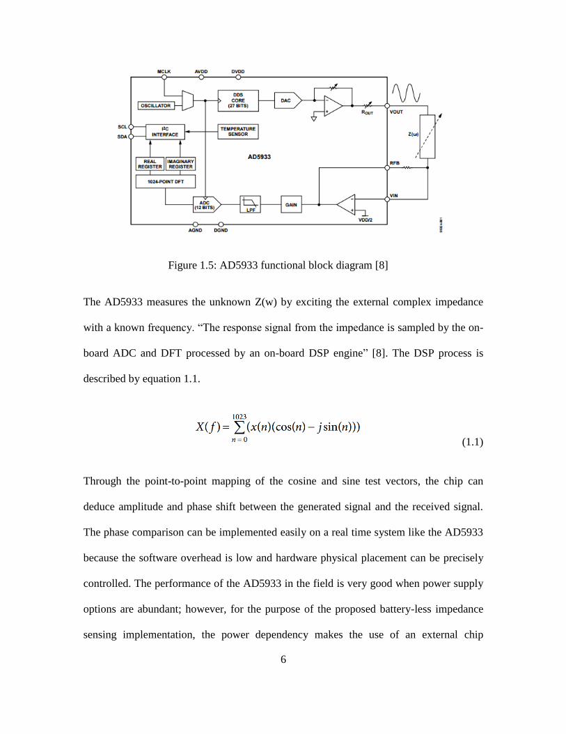
6
Figure 1.5: AD5933 functional block diagram [8]
The AD5933 measures the unknown Z(w) by exciting the external complex impedance
with a known frequency. “The response signal from the impedance is sampled by the on-
board ADC and DFT processed by an on-board DSP engine” [8]. The DSP process is
described by equation 1.1.
(1.1)
Through the point-to-point mapping of the cosine and sine test vectors, the chip can
deduce amplitude and phase shift between the generated signal and the received signal.
The phase comparison can be implemented easily on a real time system like the AD5933
because the software overhead is low and hardware physical placement can be precisely
controlled. The performance of the AD5933 in the field is very good when power supply
options are abundant; however, for the purpose of the proposed battery-less impedance
sensing implementation, the power dependency makes the use of an external chip
7
infeasible although some successful demonstrations of energy harvesting have been done
in the recent years. [9]
1.4 Stereo Soundcard RLC Measurement
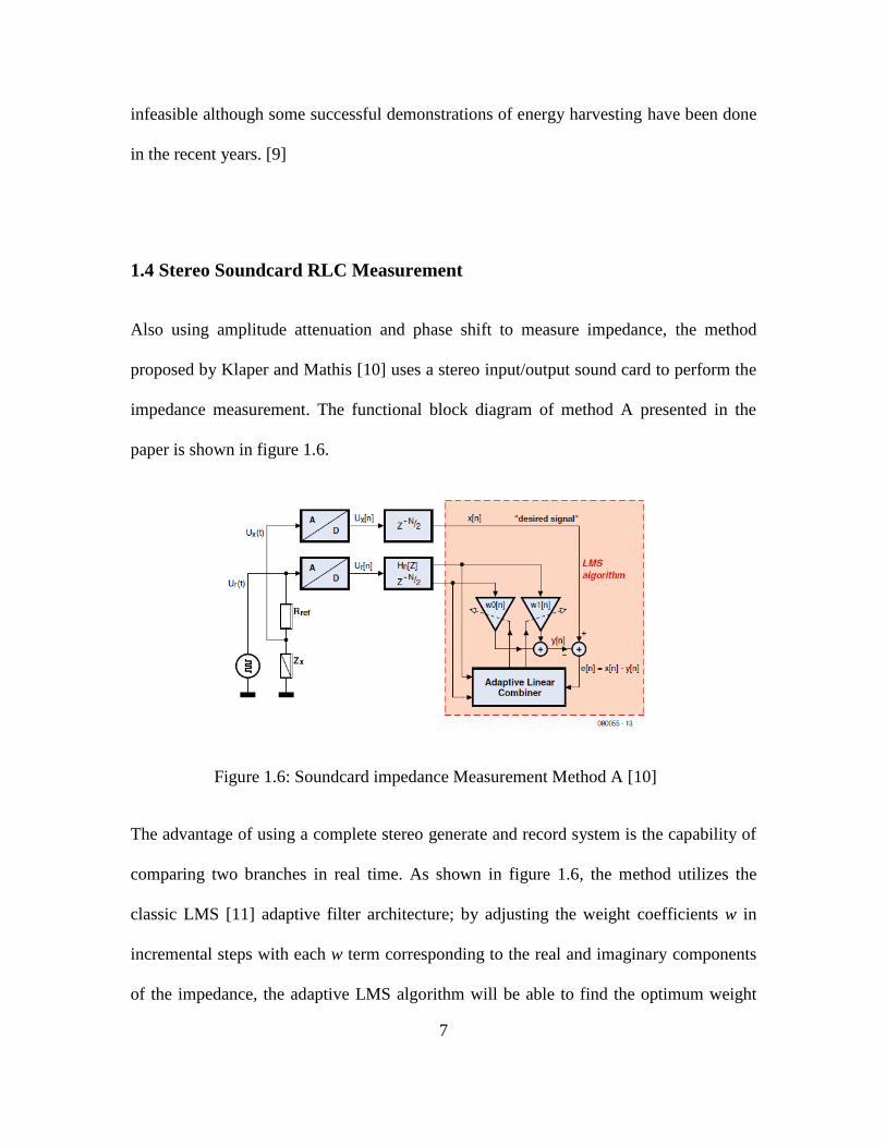
Also using amplitude attenuation and phase shift to measure impedance, the method
proposed by Klaper and Mathis [10] uses a stereo input/output sound card to perform the
impedance measurement. The functional block diagram of method A presented in the
paper is shown in figure 1.6.
Figure 1.6: Soundcard impedance Measurement Method A [10]
The advantage of using a complete stereo generate and record system is the capability of
comparing two branches in real time. As shown in figure 1.6, the method utilizes the
classic LMS [11] adaptive filter architecture; by adjusting the weight coefficients w in
incremental steps with each w term corresponding to the real and imaginary components
of the impedance, the adaptive LMS algorithm will be able to find the optimum weight

8
coefficients which will bring the signal of interest closest to the reference signal. The
detailed description of the algorithm can be found in Klaper and Mathis’ original article
[10].
1.5 Acoustic Summing Mixer-based Impedance Sensing
With a fully stereo input/output signal generation and recording system, it is easy to
perform phase shift analysis in order to conduct impedance analysis as briefly discussed
in section1.4; however, to implement a similar acoustic impedance sensing mechanism
on general purpose smartphones is more involved. Modern day smartphones always
provide a stereo audio output on the headphone jack for listening to music, but the
microphone input channel is almost always mono (one channel) as this feature
characteristic is standardized across all smartphone and headphone manufacturers.
This thesis presents a new impedance measurement method that can be used on general
purpose handheld smartphone devices. The measurement principle behind the proposed
measurement technique is the phase shift method used in all of the examples discussed in
this chapter. By using the audio additive summing mixer circuit topology found on audio
mixer consoles and signal reconstruction techniques, this thesis demonstrates a technique
to overcome the limitations to performing impedance measurement found on general
purpose smartphone devices.
9
CHAPTER 2:
THE ANALOG MIXER
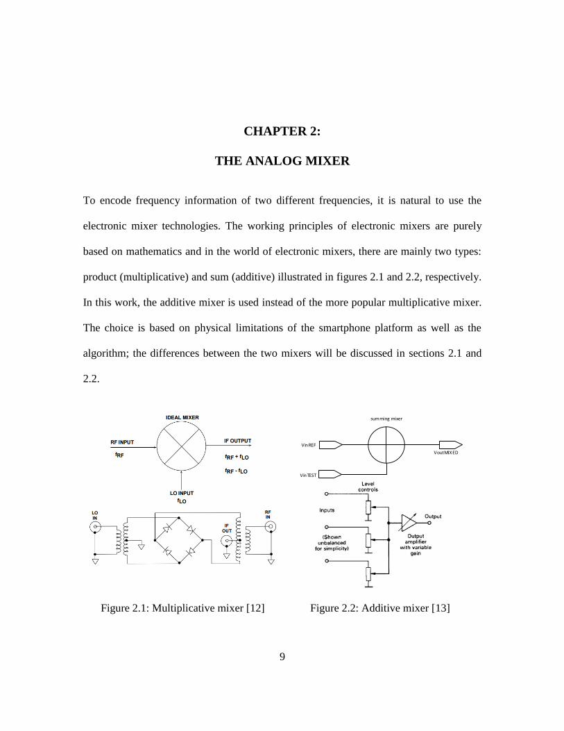
To encode frequency information of two different frequencies, it is natural to use the
electronic mixer technologies. The working principles of electronic mixers are purely
based on mathematics and in the world of electronic mixers, there are mainly two types:
product (multiplicative) and sum (additive) illustrated in figures 2.1 and 2.2, respectively.
In this work, the additive mixer is used instead of the more popular multiplicative mixer.
The choice is based on physical limitations of the smartphone platform as well as the
algorithm; the differences between the two mixers will be discussed in sections 2.1 and
2.2.
Figure 2.1: Multiplicative mixer [12] Figure 2.2: Additive mixer [13]
summing mixer
VinREF
VinTEST
VoutMIXED
10
2.1 Multiplicative Diode Mixer
The multiplicative mixer shown in figure 2.1 is predominantly used in the RF world
when high frequency information needs to be encoded in a lower frequency carrier signal
such as AM and FM radio technologies. The mathematical model of the multiplicative
mixer is simply the product of two pure tone sinusoidal signals as shown in equations 2.1
and 2.2:
1 1 2 2[ cos( )][A cos( )]oV A t t (2.1)
1 2
1 2 1 2[cos( ) cos( ) ]2
o
A AV t t (2.2)
To use a multiplicative mixer, from a mathematical point, it is desirable to have signals
with high amplitude to avoid signal attenuation due to the multiplication of amplitudes.
To overcome the signal attenuation issues, in practice, most RF transmitter/receivers will
have an RF amplifier before the filtering stages. However, in the battery-less smartphone
acoustic sensing application, it is not feasible to amplify the weak audio signals without a
DC power source. In addition to the weak output audio signals, mixing two channels
multiplicatively, it often will require a diode mixing bridge. The presence of a pair of two
diodes will further reduce the already small headroom of the audio signals by at least 300
mV if low forward drop Schottky diodes were to be used. Hence it is not reasonable to
use a traditional multiplicative frequency mixer for the application presented in this paper
despite the numerous advantages the multiplicative mixer has over the additive summing
mixer.

11
2.2 Additive Summing Mixer
The additive summing mixer shown in figure 2.2 can be found in audio applications,
mainly the audio mixing consoles used in production studios. Despite the recent
advancements in digital audio mixing consoles, the professional studio-grade consoles
are still mainly analog due to the superior audio signal fidelity that can be attained by the
additive summing mixer architecture.
Comparing the performance of the additive summing mixer to that of multiplicative
mixer as discussed in section 2.1, from the circuit’s perspective as shown in figure 2.2,
the use of a pure passive additive summing mixer will eliminate the need for the diode
bridge, thus increasing the dynamic range of the sensing system, this feature also
preserves the signal fidelity by eliminating the noise created by the diodes.
The mathematical derivation of the summing mixer is shown in equations 2.3 through 2.5.
It is important to note that the derivation shown in equations 2.3 through 2.5 is only valid
for two signals with the same amplitude magnitudes. If the two signals have different
amplitudes, the resulting mixed output will contain a series of sums of the product shown
in 2.5. The importance of matching the amplitudes of signals prior to mixing will be
discussed in greater detail in chapters 2.3 and 2.4.
1 2sin( ) sin(2 ),sin(y) sin(2 )x f t f t (2.3)
sin( ) sin( ) 2sin( )cos( )
2 2
x y x yx y
(2.4)
12
1 2 1 2
,
2 ( ) 2 ( )2sin( )cos( )
2 2 2 2out mixed
f f f fV t t
(2.5)
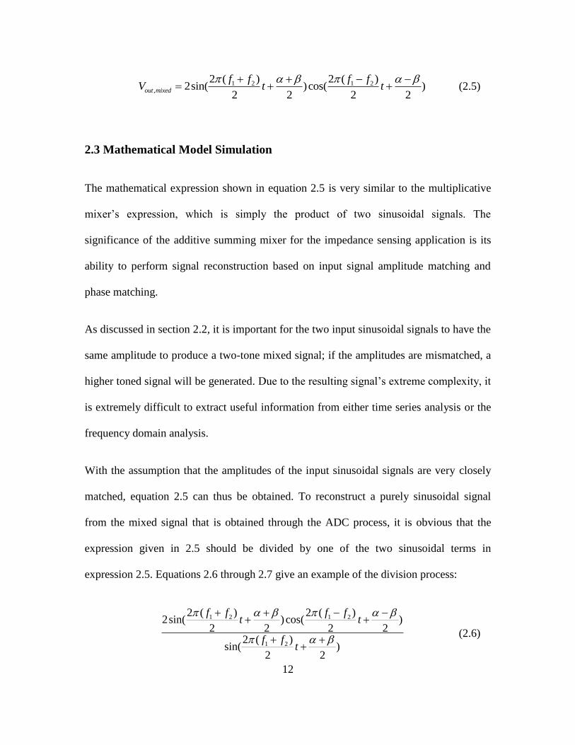
2.3 Mathematical Model Simulation
The mathematical expression shown in equation 2.5 is very similar to the multiplicative
mixer’s expression, which is simply the product of two sinusoidal signals. The
significance of the additive summing mixer for the impedance sensing application is its
ability to perform signal reconstruction based on input signal amplitude matching and
phase matching.
As discussed in section 2.2, it is important for the two input sinusoidal signals to have the
same amplitude to produce a two-tone mixed signal; if the amplitudes are mismatched, a
higher toned signal will be generated. Due to the resulting signal’s extreme complexity, it
is extremely difficult to extract useful information from either time series analysis or the
frequency domain analysis.
With the assumption that the amplitudes of the input sinusoidal signals are very closely
matched, equation 2.5 can thus be obtained. To reconstruct a purely sinusoidal signal
from the mixed signal that is obtained through the ADC process, it is obvious that the
expression given in 2.5 should be divided by one of the two sinusoidal terms in
expression 2.5. Equations 2.6 through 2.7 give an example of the division process:
1 2 1 2
1 2
2 ( ) 2 ( )2sin( ) cos( )
2 2 2 22 ( )
sin( )2 2
f f f ft t
f ft
(2.6)

13
1 22 ( )
2cos( )2 2
reconstructed
f fV t
(2.7)
At this point, the motivation of the division is very unclear because the process seems
meaningless from a purely mathematical standpoint. However, if the sets of equations are
put into real application testing scenarios, they will become very meaningful. Figure 2.3
shows the mathematical representation of the additive summing mixer and the summary
of the mathematical expression of the model.
1 1 1
2 2 2
1 2,
1 2
V sin(2 )
V sin(2 )
2 ( )V 2sin( ( ))
2 2
2 ( )cos( ( ))
2 2
in
in
out mixed
A f t
A f t
f ft
f ft
Figure 2.3: Additive summing mixer mathematical model
Figure 2.4: Additive summing mixer simulink circuit simulation
summing mixer
Vin1
Vin2
Vout,mixed
14
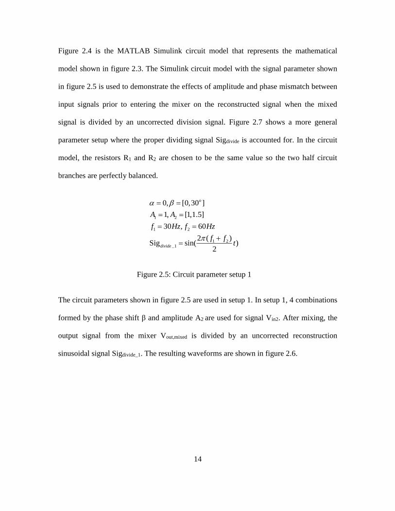
Figure 2.4 is the MATLAB Simulink circuit model that represents the mathematical
model shown in figure 2.3. The Simulink circuit model with the signal parameter shown
in figure 2.5 is used to demonstrate the effects of amplitude and phase mismatch between
input signals prior to entering the mixer on the reconstructed signal when the mixed
signal is divided by an uncorrected division signal. Figure 2.7 shows a more general
parameter setup where the proper dividing signal Sigdivide is accounted for. In the circuit
model, the resistors R1 and R2 are chosen to be the same value so the two half circuit
branches are perfectly balanced.
1 2
1 2
1 2_1
0, [0,30 ]
1, [1,1.5]
30 , 60
2 ( )Sig sin( )
2
o
divide
A A
f Hz f Hz
f ft
Figure 2.5: Circuit parameter setup 1
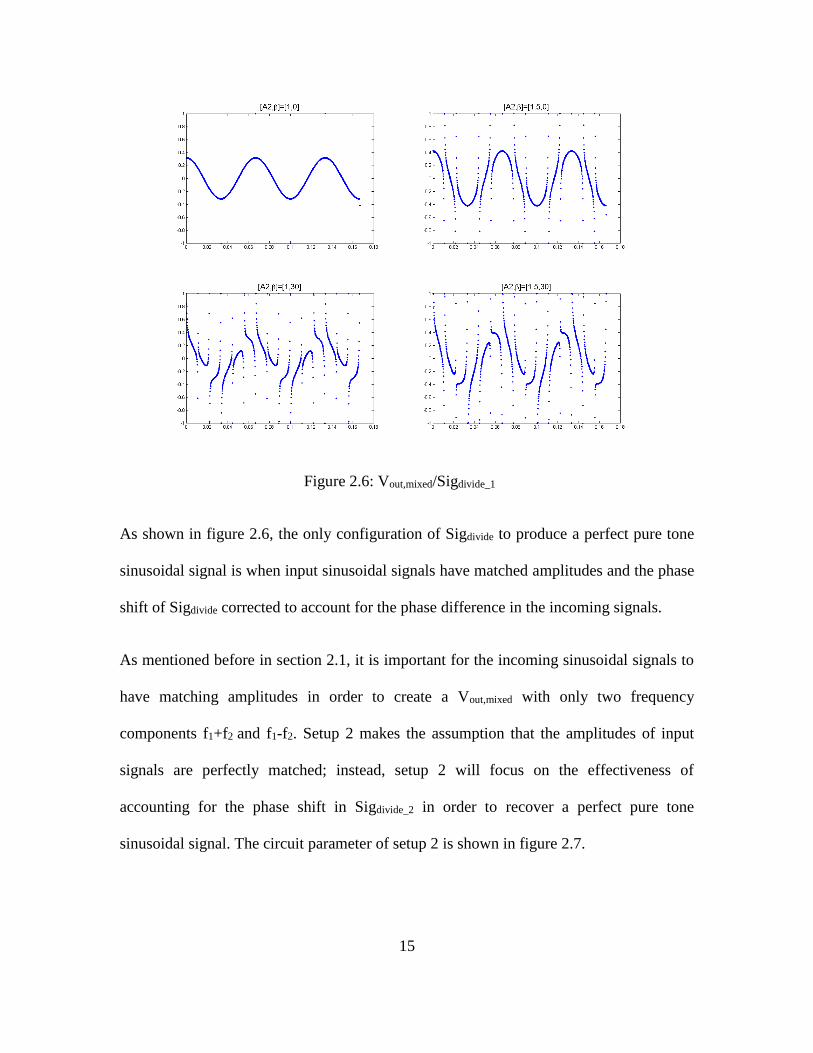
The circuit parameters shown in figure 2.5 are used in setup 1. In setup 1, 4 combinations
formed by the phase shift β and amplitude A2 are used for signal Vin2. After mixing, the
output signal from the mixer Vout,mixed is divided by an uncorrected reconstruction
sinusoidal signal Sigdivide_1. The resulting waveforms are shown in figure 2.6.
15
Figure 2.6: Vout,mixed/Sigdivide_1
As shown in figure 2.6, the only configuration of Sigdivide to produce a perfect pure tone
sinusoidal signal is when input sinusoidal signals have matched amplitudes and the phase
shift of Sigdivide corrected to account for the phase difference in the incoming signals.
As mentioned before in section 2.1, it is important for the incoming sinusoidal signals to
have matching amplitudes in order to create a Vout,mixed with only two frequency
components f1+f2 and f1-f2. Setup 2 makes the assumption that the amplitudes of input
signals are perfectly matched; instead, setup 2 will focus on the effectiveness of
accounting for the phase shift in Sigdivide_2 in order to recover a perfect pure tone
sinusoidal signal. The circuit parameter of setup 2 is shown in figure 2.7.
16
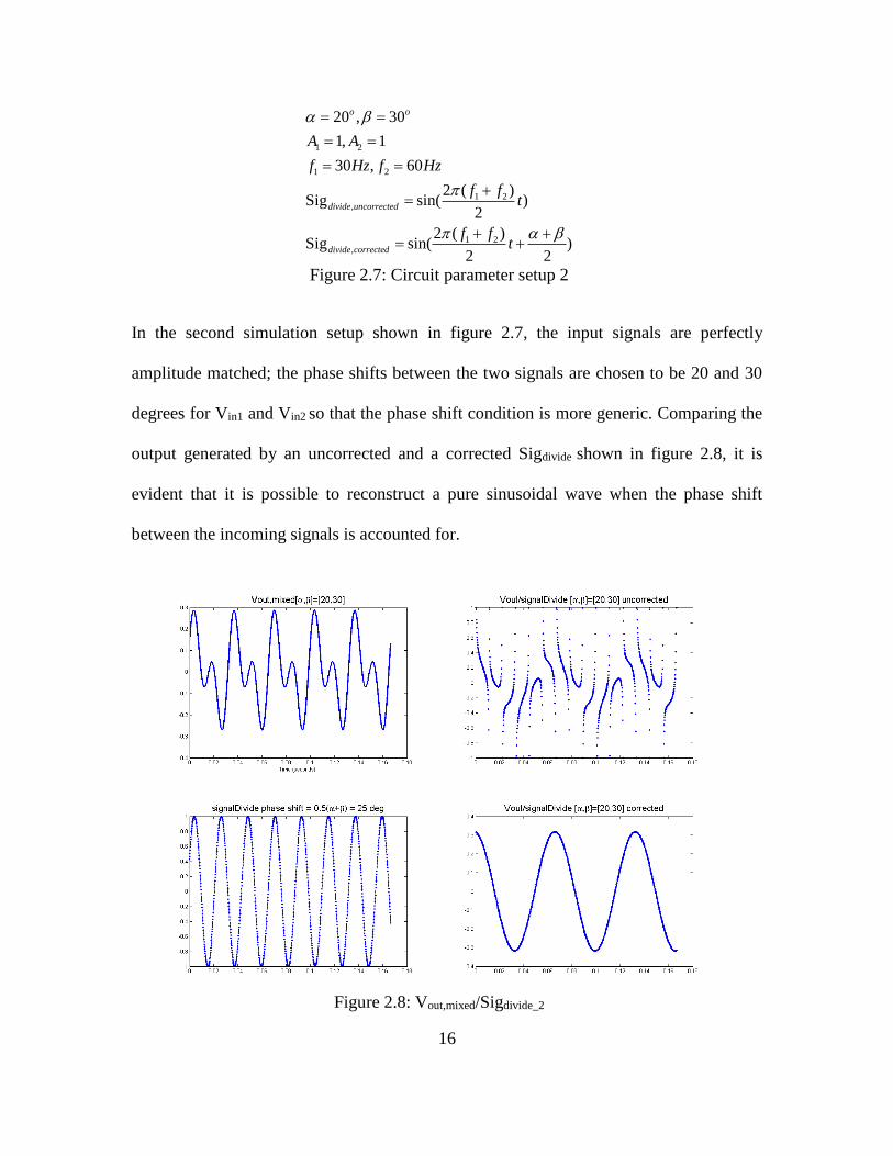
1 2
1 2
1 2,
1 2,
20 , 30
1, 1
30 , 60
2 ( )Sig sin( )
2
2 ( )Sig sin( )
2 2
o o
divide uncorrected
divide corrected
A A
f Hz f Hz
f ft
f ft
Figure 2.7: Circuit parameter setup 2
In the second simulation setup shown in figure 2.7, the input signals are perfectly
amplitude matched; the phase shifts between the two signals are chosen to be 20 and 30
degrees for Vin1 and Vin2 so that the phase shift condition is more generic. Comparing the
output generated by an uncorrected and a corrected Sigdivide shown in figure 2.8, it is
evident that it is possible to reconstruct a pure sinusoidal wave when the phase shift
between the incoming signals is accounted for.
Figure 2.8: Vout,mixed/Sigdivide_2
17
The important mathematical property behind the additive summing mixer and the process
of reconstructing the sinusoidal wave from the mixed signal are the enablers behind the
technique to implement the acoustic impedance sensing platform on the smartphone.
2.4 Phase Delayed Summing Mixer
In sections 2.2 and 2.3, the phase delay between the incoming signals are generated in
simulation through controlling the phase difference between the input signals. This is
possible in simulation to demonstrate the mathematical principle behind the summing
mixer; however, in real application of the acoustic impedance sensing platform, the phase
difference is generated through the circuit when the input signals pass through complex
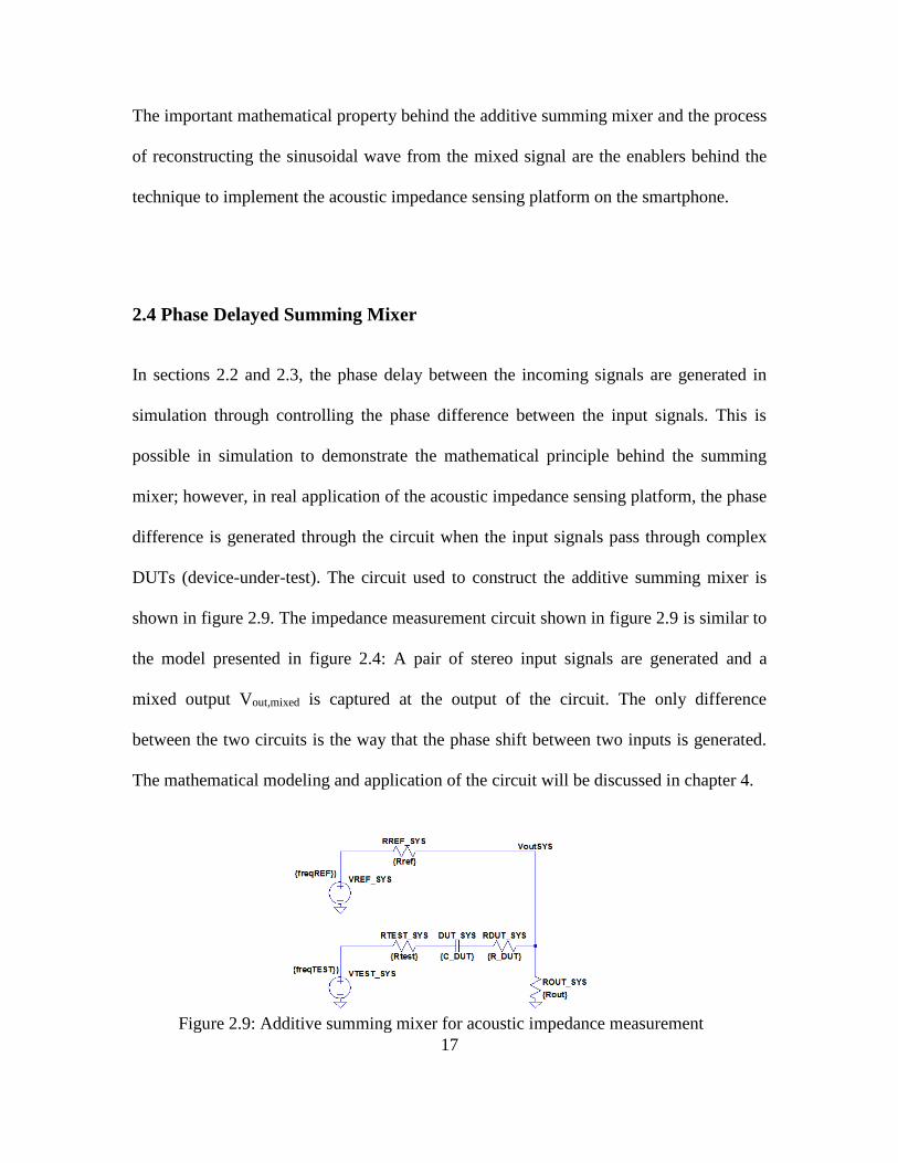
DUTs (device-under-test). The circuit used to construct the additive summing mixer is
shown in figure 2.9. The impedance measurement circuit shown in figure 2.9 is similar to
the model presented in figure 2.4: A pair of stereo input signals are generated and a
mixed output Vout,mixed is captured at the output of the circuit. The only difference
between the two circuits is the way that the phase shift between two inputs is generated.
The mathematical modeling and application of the circuit will be discussed in chapter 4.
Figure 2.9: Additive summing mixer for acoustic impedance measurement
18
CHAPTER 3:
SMARTPHONE AUDIO PERFORMANCE CHARACTERIZATIONS
In chapter 2, it is shown that it is feasible to perform sinusoidal signal reconstruction in
the additive summing mixer when the amplitudes of the input signals are perfectly
matched. Chapter 3 will be dedicated to discussing the feasibility of using a smartphone
as a test fixture platform for the acoustic impedance sensing application.
To characterize the smartphone’s capability for the impedance sensing application, the
device’s acoustic performance parameters are thoroughly examined. The acoustic
performances include: frequency response, input output voltage linearity, and output
voltage vs. reference resistance. Ultimately, when all of the measurements are combined,
it is possible to generate an adequate approximation circuit model to model the system’s
output impedance characteristics. In the smartphone test fixture setup, the system’s
output impedance is the smartphone microphone channel’s input impedance.
The smartphone used in the test setup is the Google Nexus 4 Android smartphone
manufactured by LG. In addition to the smartphone, an Agilent 33120A function
generator and a National Instruments USB-4065 programmable multimeter are used for
multi-point parametrized sweep and data acquisition. In the frequency response test, both
instruments are controlled using National Instruments LabVIEW software.

19
3.1 Output vs. Input Voltage Linearity
The first and the most fundamental characterization is the output vs input voltage
linearity test; a schematic of the test setup is shown in figure 3.1. In the output vs. input
voltage linearity test, the input voltage amplitude is incrementally adjusted from 0 to 1 V
with the step size of 50 mV. This linearity test is also repeated for five different
frequencies: 20 Hz, 30 Hz, 1 kHz, 2 kHz and 10 kHz. The output vs. input voltage sweep
plot is shown in figure 3.2.
Figure 3.1: Output vs. input voltage linearity circuit setup
Figure 3.2: Output vs. input voltage linearity plot
20
The output vs. input voltage linearity plots gathered for all frequencies are almost the
same except for the case of 10 kHz. Although the plot is still very linear, the amplitude
measured at the system output is significantly lower than that measured at the lower
frequencies. This behavior is expected of a commercial smartphone because it is
reasonable to limit the audio frequency range to the human audible range which is usually
between 10 Hz and 10 kHz. The observed signal attenuation is very possibly the effect
caused by a hardware low-pass filter. The behavior of the low-pass filter will be observed
again in the frequency response analysis in section 3.3.
From the low frequency plots, it is also possible to estimate the system output resistance
value assuming the microphone input impedance is purely resistive at low frequencies.
The estimated Rout is calculated to be 1.158 kΩ based on the slope of the best-fit line on
the 2 kHz dataset.
3.2 Output Voltage vs. Reference Resistance
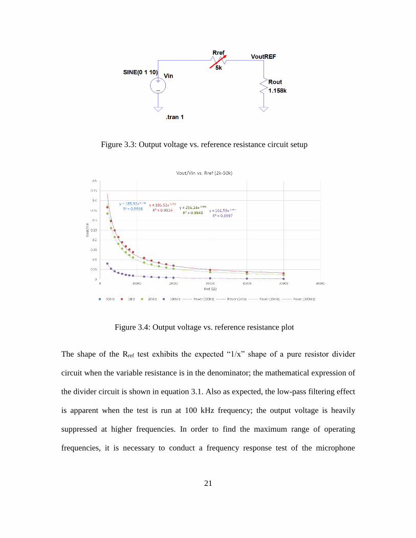
The output voltage vs. reference resistance linearity test simulates a simple resistance
measurement situation; the test circuit setup is shown in figure 3.3. The reference
resistance value Rref is swept from 2 kΩ to 50 kΩ. The resulting output voltage vs.
reference resistance plots is shown in figure 3.4. Since it has been established in section
3.1 that the system output has a low-pass filtering effect, the test frequency in the
reference resistance linearity test is pushed to 100 kHz. In the setup, a total of four
different frequencies are tested: 330 Hz, 1 kHz, 10 kHz and 100 kHz.
21
Figure 3.3: Output voltage vs. reference resistance circuit setup
Figure 3.4: Output voltage vs. reference resistance plot
The shape of the Rref test exhibits the expected “1/x” shape of a pure resistor divider
circuit when the variable resistance is in the denominator; the mathematical expression of
the divider circuit is shown in equation 3.1. Also as expected, the low-pass filtering effect
is apparent when the test is run at 100 kHz frequency; the output voltage is heavily
suppressed at higher frequencies. In order to find the maximum range of operating
frequencies, it is necessary to conduct a frequency response test of the microphone
22
channel so the impedance measurement range can be maximized or appropriately
compensated.
out out
in out ref
V R
V R R
(3.1)
3.3 Frequency Response
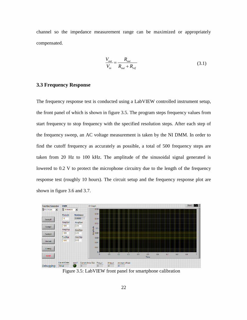
The frequency response test is conducted using a LabVIEW controlled instrument setup,
the front panel of which is shown in figure 3.5. The program steps frequency values from
start frequency to stop frequency with the specified resolution steps. After each step of
the frequency sweep, an AC voltage measurement is taken by the NI DMM. In order to
find the cutoff frequency as accurately as possible, a total of 500 frequency steps are
taken from 20 Hz to 100 kHz. The amplitude of the sinusoidal signal generated is
lowered to 0.2 V to protect the microphone circuitry due to the length of the frequency
response test (roughly 10 hours). The circuit setup and the frequency response plot are
shown in figure 3.6 and 3.7.
Figure 3.5: LabVIEW front panel for smartphone calibration
23
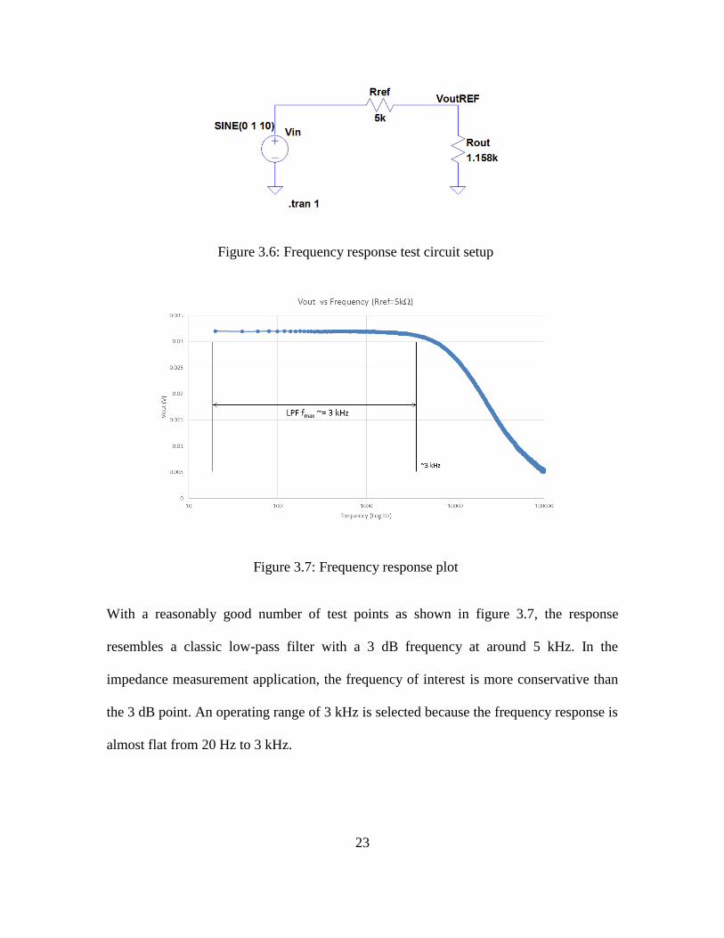
Figure 3.6: Frequency response test circuit setup
Figure 3.7: Frequency response plot
With a reasonably good number of test points as shown in figure 3.7, the response
resembles a classic low-pass filter with a 3 dB frequency at around 5 kHz. In the
impedance measurement application, the frequency of interest is more conservative than
the 3 dB point. An operating range of 3 kHz is selected because the frequency response is
almost flat from 20 Hz to 3 kHz.
24
3.4 Modeling Unknown Microphone Input Resistance
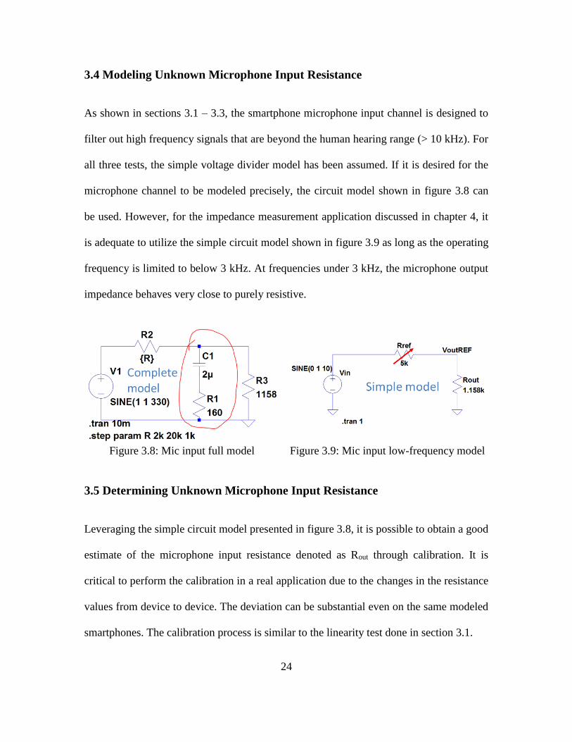
As shown in sections 3.1 – 3.3, the smartphone microphone input channel is designed to
filter out high frequency signals that are beyond the human hearing range (> 10 kHz). For
all three tests, the simple voltage divider model has been assumed. If it is desired for the
microphone channel to be modeled precisely, the circuit model shown in figure 3.8 can
be used. However, for the impedance measurement application discussed in chapter 4, it
is adequate to utilize the simple circuit model shown in figure 3.9 as long as the operating
frequency is limited to below 3 kHz. At frequencies under 3 kHz, the microphone output
impedance behaves very close to purely resistive.
Figure 3.8: Mic input full model Figure 3.9: Mic input low-frequency model
3.5 Determining Unknown Microphone Input Resistance
Leveraging the simple circuit model presented in figure 3.8, it is possible to obtain a good
estimate of the microphone input resistance denoted as Rout through calibration. It is
critical to perform the calibration in a real application due to the changes in the resistance
values from device to device. The deviation can be substantial even on the same modeled
smartphones. The calibration process is similar to the linearity test done in section 3.1.
25
CHAPTER 4:
IMPEDANCE DETECTION ALGORITHM
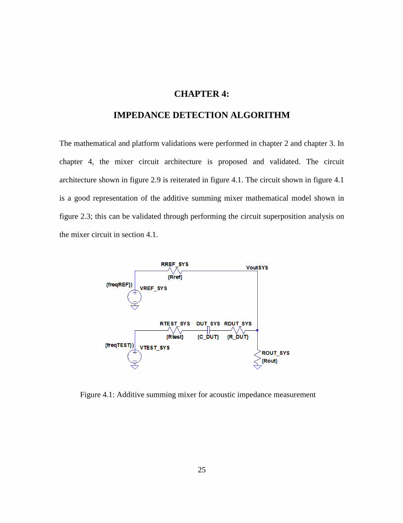
The mathematical and platform validations were performed in chapter 2 and chapter 3. In
chapter 4, the mixer circuit architecture is proposed and validated. The circuit
architecture shown in figure 2.9 is reiterated in figure 4.1. The circuit shown in figure 4.1
is a good representation of the additive summing mixer mathematical model shown in
figure 2.3; this can be validated through performing the circuit superposition analysis on
the mixer circuit in section 4.1.
Figure 4.1: Additive summing mixer for acoustic impedance measurement

26
4.1 Superposition Circuit Modeling
The additive summing mixer circuit shown in figure 4.1 can be decomposed into two
branches through the Thevenin circuit superposition theory. The superposition equivalent
circuits of figure 4.1 are shown in figure 4.2.
Figure 4.2: Superposition circuits of the additive summing mixer circuit
“The superposition theorem for electrical circuit states that for a linear system the
response (voltage or current) in any branch of a bilateral linear circuit having more than
one independent source equals the algebraic sum of the responses caused by each
independent source acting alone, where all the other independent sources are replaced by
their internal impedances” [14]. For the additive summing mixer circuit shown in figure
4.1, the superposition equivalent circuits shown in figure 4.2 are generated by
suppressing one voltage source at a time and adding the nodes of interest together to
reconstruct the original circuit’s behavior. In figures 4.1 and 4.2, each voltage source
represents a single stereo audio channel that is also a part of the 3.5 mm headphone jack.
The superposition equivalent models are simulated and compared to the full mixer circuit
model with real DUT test scenarios to replicate a real testing environment. Figure 4.3
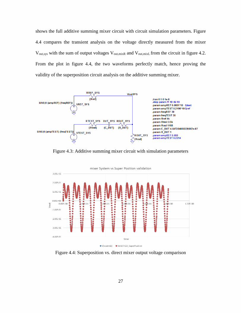
27
shows the full additive summing mixer circuit with circuit simulation parameters. Figure
4.4 compares the transient analysis on the voltage directly measured from the mixer
Vout,sys with the sum of output voltages Vout,mixR and Vout,mixL from the circuit in figure 4.2.
From the plot in figure 4.4, the two waveforms perfectly match, hence proving the
validity of the superposition circuit analysis on the additive summing mixer.
Figure 4.3: Additive summing mixer circuit with simulation parameters
Figure 4.4: Superposition vs. direct mixer output voltage comparison
28
4.2 Impedance Response and Look-Up Table
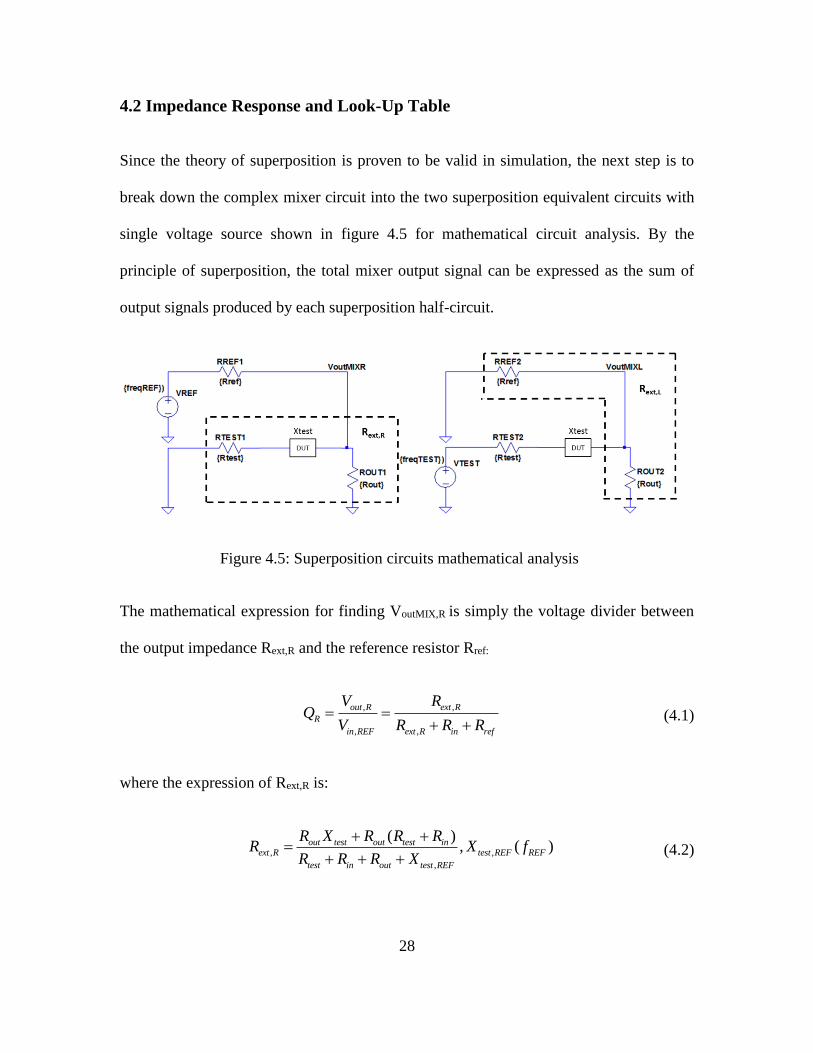
Since the theory of superposition is proven to be valid in simulation, the next step is to
break down the complex mixer circuit into the two superposition equivalent circuits with
single voltage source shown in figure 4.5 for mathematical circuit analysis. By the
principle of superposition, the total mixer output signal can be expressed as the sum of
output signals produced by each superposition half-circuit.
Figure 4.5: Superposition circuits mathematical analysis
The mathematical expression for finding VoutMIX,R is simply the voltage divider between
the output impedance Rext,R and the reference resistor Rref:
, ,
, ,
out R ext R
R
in REF ext R in ref
V RQ
V R R R
(4.1)
where the expression of Rext,R is:
, ,
,
( ), ( )out test out test in
ext R test REF REF
test in out test REF
R X R R RR X f
R R R X
(4.2)

29
Similarly for the right channel half-circuit, the VoutMIX,L can also be expressed using
voltage divider between Rtest, Xtest and Rext,:
,L ,L
,TEST ,L
, ( )out ext
L test test
in ext in test test
V RQ X f
V R R R X
(4.3)
where Rext,L can be expressed as:
,L
( )out ref in
ext
ref in out
R R RR
R R R
(4.4)
In both the reference channel and test channel, resistance Rin is a built-in stereo output
resistance of 20 Ω; this resistance can be ignored in calculations.
In each half-circuit, the only unknown variable is the impedance of the DUT Xtest.
Assuming Xtest is purely reactive with only imaginary component of the impedance, Xtest
can be expressed as equation 4.5, where ΩDUT > 0 when DUT is net inductive and ΩDUT <
0 when DUT is net capacitive. The sign of ΩDUT does not affect the amplitude of the
output voltages, but it does affect the phase shift of the output voltages. With the above
assumption, each half-circuit mathematical expression reduces down to a single variable
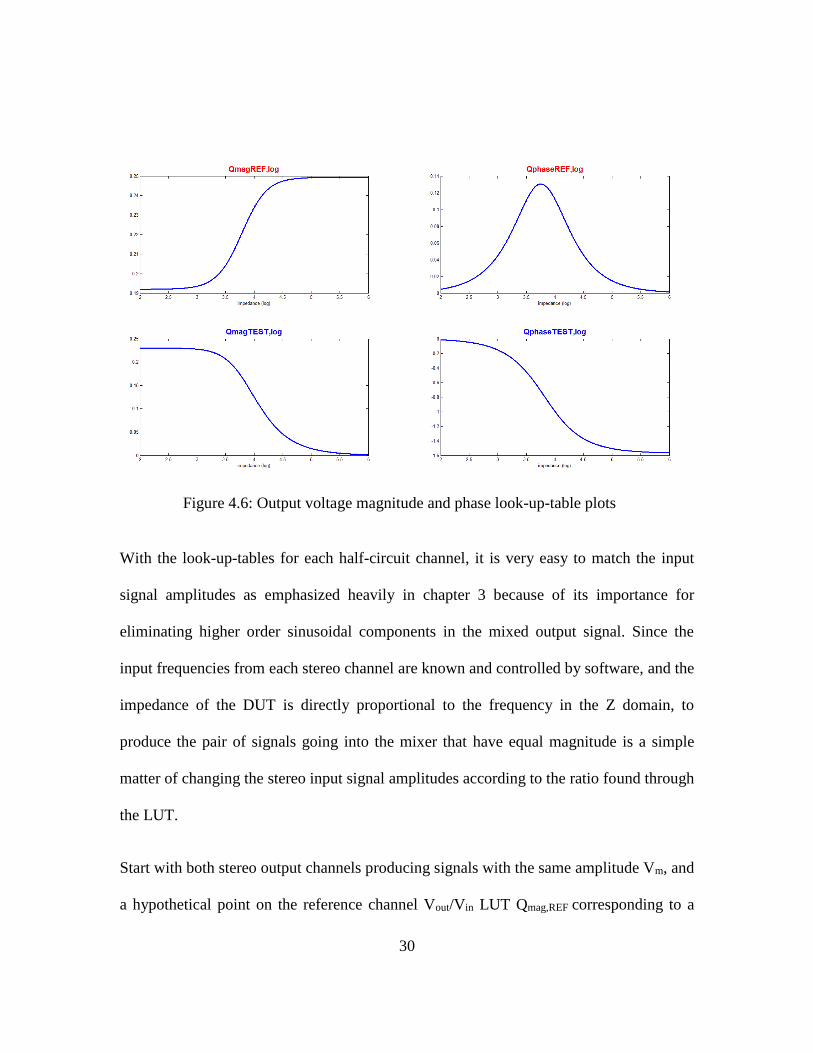
one-to-one function; hence, two sets of output voltage magnitude and phase look-up-
tables based on the impedance value ΩDUT can be generated for each half-circuit as shown
in figure 4.6.
test DUTX j (4.5)
30
Figure 4.6: Output voltage magnitude and phase look-up-table plots
With the look-up-tables for each half-circuit channel, it is very easy to match the input
signal amplitudes as emphasized heavily in chapter 3 because of its importance for
eliminating higher order sinusoidal components in the mixed output signal. Since the
input frequencies from each stereo channel are known and controlled by software, and the
impedance of the DUT is directly proportional to the frequency in the Z domain, to
produce the pair of signals going into the mixer that have equal magnitude is a simple
matter of changing the stereo input signal amplitudes according to the ratio found through
the LUT.
Start with both stereo output channels producing signals with the same amplitude Vm, and
a hypothetical point on the reference channel Vout/Vin LUT Qmag,REF corresponding to a
31
impedance value of roughly ZDUT,REF. With the impedance found on the reference channel,
the impedance of the same DUT seen by the test channel is:
, ,
TESTDUT TEST DUT REF
REF
fZ Z
f (4.6)
With the impedance value seen by the test channel ZDUT,TEST, the Vout/Vin response of the
test channel can be found on the Qmag,TEST plot. With the Vout/Vin ratios obtained for both
the reference and test channels, the amplitudes generated by the stereo channels can be
found using equation 4.7. The pair of amplitudes found by 4.7 will ensure that the
immediate incoming signals for the additive summing mixer have the same amplitude,
thus satisfying the amplitude matching rule.
,TEST
,
mag
REF m
mag REF
QV V
Q ,
,
,TEST
mag REF
TEST m
mag
QV V
Q (4.7)
At this point, it is assumed that the Vout/Vin plot for either of the two channels is known,
but in fact, it is impossible to obtain a direct measurement of the Vout/Vin on either
channel because the summing mixer cannot be broken into the two physical circuits
shown in figure 4.5. To bridge simulation and reality, a third LUT from the circuit shown
in figure 4.7 is needed. The circuit equivalent shown in figure 4.7 can be physically
obtained by turning off the reference channel to form a true mono configuration.
32
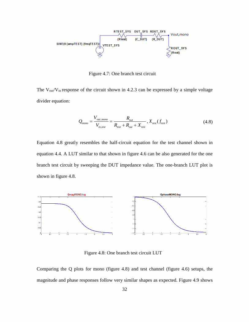
Figure 4.7: One branch test circuit
The Vout/Vin response of the circuit shown in 4.2.3 can be expressed by a simple voltage
divider equation:
,
,
, ( )out mono out
mono test test
in test test out test
V RQ X f
V R R X
(4.8)
Equation 4.8 greatly resembles the half-circuit equation for the test channel shown in
equation 4.4. A LUT similar to that shown in figure 4.6 can be also generated for the one
branch test circuit by sweeping the DUT impedance value. The one-branch LUT plot is
shown in figure 4.8.
Figure 4.8: One branch test circuit LUT
Comparing the Q plots for mono (figure 4.8) and test channel (figure 4.6) setups, the
magnitude and phase responses follow very similar shapes as expected. Figure 4.9 shows
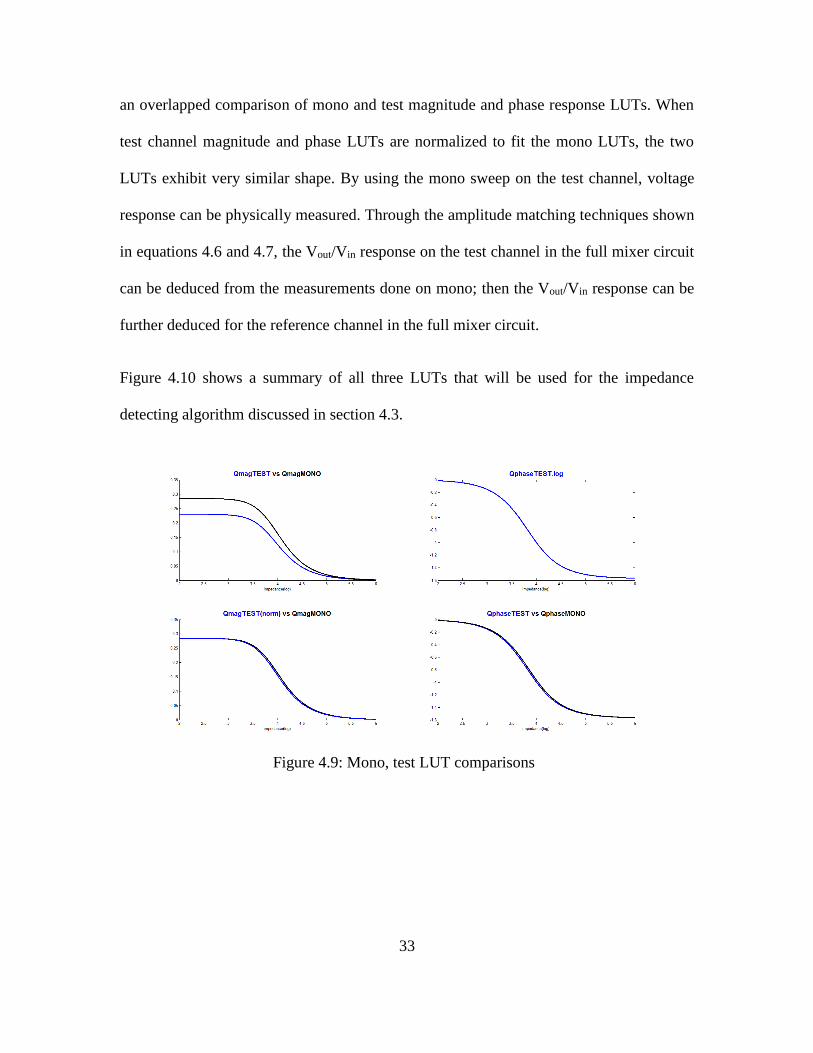
33
an overlapped comparison of mono and test magnitude and phase response LUTs. When
test channel magnitude and phase LUTs are normalized to fit the mono LUTs, the two
LUTs exhibit very similar shape. By using the mono sweep on the test channel, voltage
response can be physically measured. Through the amplitude matching techniques shown
in equations 4.6 and 4.7, the Vout/Vin response on the test channel in the full mixer circuit
can be deduced from the measurements done on mono; then the Vout/Vin response can be
further deduced for the reference channel in the full mixer circuit.
Figure 4.10 shows a summary of all three LUTs that will be used for the impedance
detecting algorithm discussed in section 4.3.
Figure 4.9: Mono, test LUT comparisons

34
Figure 4.10: REF, TEST, mono LUT summary
4.3 Unknown Impedance Detection: Algorithm Overview
There are four main steps involved in the additive summing mixer based impedance
measurement algorithm:
1. Characterize device microphone input resistance Rout (section 3.5).
2. Generate look-up tables for mixer half circuits and mono test circuit (section 4.2).
3. Perform frequency sweep on mono channel to obtain a suitable point on mono LUT
and calculate LCR.
4. Find amplitude and phase shift for mixer superposition circuits, and derive the
35
reconstruction waveform to check results (section 2.3).
Steps 1 and 2 will be briefly summarized as these were topics discussed in previous
chapters. It is necessary to characterize each smartphone device without DUT attached as
step 1 because the microphone input impedance Rout is a critical component in the LUT
generation done in step 2. The mic impedance can be found by the methods described in
section 3.5. After Rout is available, step 2 is purely based on circuit model and
mathematics. With all the resistive elements either provided by the user or determined in
step 1, the only unknown variable in the circuit model is the DUT impedance, so the
impedance value is used to generate the Vout amplitude and phase LUTs for the three
aforementioned circuit setups shown in section 4.2.
Step 3 is the most important step in the entire algorithm and involves iterating through
different frequencies to narrow down on the frequency that will obtain an optimal DUT
impedance point on the mono LUT shown in figure 4.8. Provided an unknown DUT that
is either capacitive or inductive, the DUT’s impedance can be controlled by adjusting the
input sinusoidal signal frequency. Also, through the frequency spectroscopy analysis, the
DUT’s electrical characteristics can be obtained. Taking the mono test circuit setup
shown in figure 4.7 as an example, if the DUT is net capacitive, the output voltage will be
positively related to input signal frequency because the impedance of capacitive devices
is inversely related to incident frequency; the opposite is true for inductive devices, and if
the frequency response is flat, then the DUT can be modeled as a purely resistive device.
The frequency spectroscopy analysis used in this discussion assumes the frequencies are
low enough that resonance is avoided where possible.
36
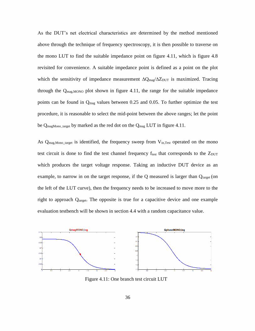
As the DUT’s net electrical characteristics are determined by the method mentioned
above through the technique of frequency spectroscopy, it is then possible to traverse on
the mono LUT to find the suitable impedance point on figure 4.11, which is figure 4.8
revisited for convenience. A suitable impedance point is defined as a point on the plot
which the sensitivity of impedance measurement ∆Qmag/∆ZDUT is maximized. Tracing
through the Qmag,MONO plot shown in figure 4.11, the range for the suitable impedance
points can be found in Qmag values between 0.25 and 0.05. To further optimize the test
procedure, it is reasonable to select the mid-point between the above ranges; let the point
be QmagMono_target by marked as the red dot on the Qmag LUT in figure 4.11.
As Qmag,Mono_target is identified, the frequency sweep from Vin,Test operated on the mono
test circuit is done to find the test channel frequency ftest that corresponds to the ZDUT
which produces the target voltage response. Taking an inductive DUT device as an
example, to narrow in on the target response, if the Q measured is larger than Qtarget (on
the left of the LUT curve), then the frequency needs to be increased to move more to the
right to approach Qtarget. The opposite is true for a capacitive device and one example
evaluation testbench will be shown in section 4.4 with a random capacitance value.
Figure 4.11: One branch test circuit LUT
37
After the target impedance frequency pair has been acquired, it is possible to back-
calculate the capacitance or inductance value at this point if the device is purely
imaginary with no real component. It is always necessary to use the additive summing
mixer signal reconstruction technique to check the impedance results obtained through
the mono test. Also, for complex impedance systems with real and imaginary components,
it is very difficult to accurately characterize the system with mono-only test setup.
To test the impedance result obtained through the mono test using the full additive
summing mixer, appropriate amplitudes and phases for both reference and test channels
are needed for the reconstruction equation. As mentioned in section 4.2 and seen in
equation 4.7, the voltages are simply the ratios of Qmag found for each channel through
LUT process initialized by the Mono LUT as described in section 4.2. The expression for
the reconstruction equation is shown in equation 4.9 which is a reiterated version of
Sigdivide,corrected shown in figure 2.5 where pref and ptest can both be looked up from each
half-circuit LUT:
sin(2 )
2 2
ref test ref test
divide
f f p pSig t
(4.9)
If the corrected signal generated by dividing the mixed signal by Sigdivide is very close to
a pure tone sinusoidal signal, then the impedance measurement is successful. Section 4.4
will provide an example of a simulated measurement procedure.
38
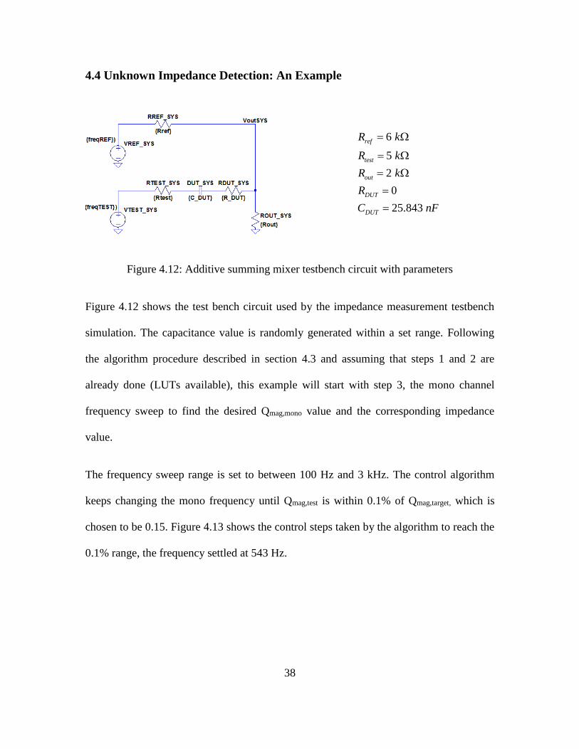
4.4 Unknown Impedance Detection: An Example
6
5
2
25.843
0
ref
test
o
DU
u
UT
T
t
D
R k
R k
R k
C nF
R
Figure 4.12: Additive summing mixer testbench circuit with parameters
Figure 4.12 shows the test bench circuit used by the impedance measurement testbench
simulation. The capacitance value is randomly generated within a set range. Following
the algorithm procedure described in section 4.3 and assuming that steps 1 and 2 are
already done (LUTs available), this example will start with step 3, the mono channel
frequency sweep to find the desired Qmag,mono value and the corresponding impedance
value.
The frequency sweep range is set to between 100 Hz and 3 kHz. The control algorithm
keeps changing the mono frequency until Qmag,test is within 0.1% of Qmag,target, which is
chosen to be 0.15. Figure 4.13 shows the control steps taken by the algorithm to reach the
0.1% range, the frequency settled at 543 Hz.

39
Figure 4.13: Frequency vs. control step for mono frequency sweep
After using the LUTs generated for the superposition half circuits, fref, ftest, Pref and Ptest
are found and tabulated in figure 4.14. Figure 4.15 shows the signal produced measured
at the output of the mixer. Figure 4.16 shows the reconstructed signal with close
resemblance to a pure tone sinusoidal signal. With the reconstructed signal being
sinusoidal as the primary indication of successful measurement, in addition, the
capacitance value that is calculated from the algorithm is 25.827 nF, very close to the
actual device capacitance of 25.843 nF.
452.54 Hz
543.04 Hz
ref
test
f
f
0.0934 rad
1.0492 rad
ref
test
P
P
Figure 4.14: Summary of input signal properties

40
Figure 4.15: Voltage output from mixer Vout,mixed
Figure 4.16: Reconstructed signal after division

41
CHAPTER 5:
SUMMARY AND FUTURE WORK
The additive summing mixer based impedance measurement method presented in this
work is able to accurately characterize the DUT’s device characteristics. The smartphone
based summing mixer method is advantageous because the circuit is purely dependent on
the stereo signals generated by the smartphone’s audio jack, thus making the circuit
battery-less.
In addition to the smartphone focused implementation presented in this paper, the mixer
based impedance measurement method can be very flexibly implemented on any system
with stereo signal generation and mono reception because the method presented is purely
mathematical.
For future work, the impedance measurement functionality of the software needs to be
expanded so the system can measure more complex impedance systems that contain
DUTs with both real and imaginary impedance components. Also, the smartphone’s
internet capability can be leveraged so that the impedance measurement can be
implemented for medical sensing and diagnosis such as breast cancer self-diagnosis.

42
REFERENCES
[1] Wikipedia, "Electrical impedance," https://en.wikipedia.org/wiki/Electrical_impedance.
[2] O. Heaviside, in Electrical Papers, The Electrician Printing and Publishing Co, 1886, p. 212.
[3] H. Schwan, "Electrical properties of body tissues and impedance plethysmography," IRE Transactions
on Medical Electronics, Vols. PGME-3, no. 1955, pp. 32 - 46, 1955.
[4] W. Tong and W. W. Tang, "Measuring impedance in congestive heart failure: Current," Am Heart,
vol. 157, no. 3, pp. 402-411, 2009.
[5] M. Elgendi, "On the analysis of fingertip photoplethysmogram signals," Current Cardiology Reviews,
vol. 8, no. 1, 2012.
[6] P. Shaltis, A. Reisner and H. Asada, "Calibration of the Photoplethysmogram to Arterial Blood
Pressure: Capabilities and Limitations for Continuous Pressure Monitoring," in Engineering in
Medicine and Biology 27th Annual Conference, Shanghai, China, 2005.
[7] Agilent Impedance Measurement Handbook, 4th Edition, Santa Clara, CA: Agilent Technologies,
2013.
[8] Analog Devices, "1 MSPS, 12-bit impedance converter, network analyzer," AD5933 datasheet, Sept
2005 [Revised May. 2013].
[9] Y.-S. Kuo, T. Schmid and P. Dutta, "Hijacking power and bandwidth from the mobile phone’s audio
interface," in International Symposium on Low Power Electronics and Design, 2010.
[10] M. Klaper and H. Mathis, "2-Pound RLC meter impedance measurement using a sound card," elektor,
June 2008.
[11] S. Haykin and B. Widrow, Least-Mean-Square Adaptive Filters, Hoboken, NJ, USA: John Wiley &
Sons, Inc, 2003.
[12] Analog Devices, Linear Circuit Design Handbook, Norwood, MA: Analog Devices, 2008.
[13] T. Michael, Audio Engineer's Reference Book, 2nd ed, Burlington, MA: Focal Press, 2013.
[14] Wikipedia, "Superposition theorem," https://en.wikipedia.org/wiki/Superposition_theorem.