sn65hvd2x extended common-mode rs-485 … · 2 sn65hvd20, sn65hvd21, sn65hvd22, sn65hvd23,...
TRANSCRIPT

0.1
1
10
100
HVD20
HVD23
HVD24
HVD21
HVD22
Sig
na
ling
Ra
te -
Mb
ps
10 100 1000
Cable Length - m
-20 V +25 V
-7 V +12 V
SUPER485
RS485
-20 V -15 V -10 V -5 V 0 5 V 10 V 15 V 20 V 25 V
Product
Folder
Sample &Buy
Technical
Documents
Tools &
Software
Support &Community
ReferenceDesign
An IMPORTANT NOTICE at the end of this data sheet addresses availability, warranty, changes, use in safety-critical applications,intellectual property matters and other important disclaimers. PRODUCTION DATA.
SN65HVD20, SN65HVD21, SN65HVD22, SN65HVD23, SN65HVD24SLLS552F –DECEMBER 2002–REVISED NOVEMBER 2016
SN65HVD2x Extended Common-Mode RS-485 Transceivers
1
1 Features1• Common-Mode Voltage Range (–20 V to 25 V)
More Than Doubles TIA/EIA-485 Requirement• Receiver Equalization Extends Cable Length,
Signaling Rate (SN65HVD2[3,4])• Reduced Unit-Load for up to 256 Nodes• Bus I/O Protection to Over 16-kV HBM• Failsafe Receiver for Open-Circuit, Short-Circuit,
and Idle-Bus Conditions• Low Standby Supply Current 1 µA (Maximum)• More Than 100 mV Receiver Hysteresis
2 Applications• Long Cable Solutions
– Factory Automation– Security Networks– Building HVAC
• Severe Electrical Environments– Electrical Power Inverters– Industrial Drives– Avionics
3 DescriptionThe transceivers in the SN65HVD2x family offerperformance far exceeding typical RS-485 devices. Inaddition to meeting all requirements of theTIA/EIA‑485-A standard. The SN65HVD2x familyoperates over an extended range of common-modevoltages and has features such as high ESDprotection, wide receiver hysteresis, and failsafeoperation. This family of devices is ideally suited forlong-cable networks and other applications where theenvironment is too harsh for ordinary transceivers.
These devices are designed for bidirectional datatransmission on multipoint twisted-pair cables.Example applications are digital motor controllers,remote sensors and terminals, industrial processcontrol, security stations, and environmental controlsystems.
These devices combine a 3-state differential driverand a differential receiver that operate from a single5-V power supply. The driver differential outputs andthe receiver differential inputs are connectedinternally to form a differential bus port that offersminimum loading to the bus. This port features anextended common-mode voltage range, making thedevice suitable for multipoint applications over longcable runs.
Device Information(1)
PART NUMBER PACKAGE BODY SIZE (NOM)
SN65HVD2xSOIC (8) 4.90 mm × 3.91 mmPDIP (8) 9.81 mm × 6.35 mm
(1) For all available packages, see the orderable addendum atthe end of the data sheet.
SN65HVD2x Application Space SN65HVD2x Devices Operate Over a WiderCommon-Mode Voltage Range

2
SN65HVD20, SN65HVD21, SN65HVD22, SN65HVD23, SN65HVD24SLLS552F –DECEMBER 2002–REVISED NOVEMBER 2016 www.ti.com
Product Folder Links: SN65HVD20 SN65HVD21 SN65HVD22 SN65HVD23 SN65HVD24
Submit Documentation Feedback Copyright © 2002–2016, Texas Instruments Incorporated
Table of Contents1 Features .................................................................. 12 Applications ........................................................... 13 Description ............................................................. 14 Revision History..................................................... 25 Description (continued)......................................... 46 Device Options....................................................... 47 Pin Configuration and Functions ......................... 58 Specifications......................................................... 5
8.1 Absolute Maximum Ratings ...................................... 58.2 ESD Ratings.............................................................. 68.3 Recommended Operating Conditions....................... 68.4 Thermal Information .................................................. 78.5 Driver Electrical Characteristics ................................ 78.6 Receiver Electrical Characteristics ........................... 88.7 Driver Switching Characteristics ............................... 88.8 Receiver Switching Characteristics........................... 98.9 Receiver Equalization Characteristics ...................... 98.10 Power Dissipation ................................................. 108.11 Typical Characteristics .......................................... 11
9 Parameter Measurement Information ................ 12
10 Detailed Description ........................................... 1710.1 Overview ............................................................... 1710.2 Functional Block Diagram ..................................... 1710.3 Feature Description............................................... 1710.4 Device Functional Modes...................................... 19
11 Application and Implementation........................ 2211.1 Application Information.......................................... 2211.2 Typical Application ................................................ 22
12 Power Supply Recommendations ..................... 2413 Layout................................................................... 24
13.1 Layout Guidelines ................................................. 2413.2 Layout Example .................................................... 25
14 Device and Documentation Support ................. 2614.1 Related Links ........................................................ 2614.2 Receiving Notification of Documentation Updates 2614.3 Community Resources.......................................... 2614.4 Trademarks ........................................................... 2614.5 Electrostatic Discharge Caution............................ 2614.6 Glossary ................................................................ 26
15 Mechanical, Packaging, and OrderableInformation ........................................................... 26
4 Revision HistoryNOTE: Page numbers for previous revisions may differ from page numbers in the current version.
Changes from Revision E (May 2010) to Revision F Page
• Added ESD Ratings table, Feature Description section, Device Functional Modes, Application and Implementationsection, Power Supply Recommendations section, Layout section, Device and Documentation Support section, andMechanical, Packaging, and Orderable Information section. ................................................................................................. 1
• Deleted Ordering Information table; see POA at the end of the data sheet........................................................................... 1• Added maximum temperature value (150°C) to "Storage temperate, Tstg parameter............................................................ 5
Changes from Revision D (April 2005) to Revision E Page
• Replaced the Dissipation Rating table with the THERMAL INFORMATION table................................................................. 7• Changed IO - Added test condition and values per device number (DRIVER ELECTRICAL CHARACTERISTICS table) ... 7• Changed the THERMAL CHARACTERISTICS table to POWER DISSIPATION table ....................................................... 10• Added the TEST MODE DRIVER DISABLE section............................................................................................................ 20
Changes from Revision C (September 2003) to Revision D Page
• Added Conditions note to the ABSOLUTE MAXIMUM RATINGS table "over operating free-air temperature range(unless otherwise noted)" ....................................................................................................................................................... 5
• Deleted Storage temperature, Tstg from the ABSOLUTE MAXIMUM RATINGS table........................................................... 5• Added Receiver output current, IO to the ABSOLUTE MAXIMUM RATINGS table ............................................................... 5
3
SN65HVD20, SN65HVD21, SN65HVD22, SN65HVD23, SN65HVD24www.ti.com SLLS552F –DECEMBER 2002–REVISED NOVEMBER 2016
Product Folder Links: SN65HVD20 SN65HVD21 SN65HVD22 SN65HVD23 SN65HVD24
Submit Documentation FeedbackCopyright © 2002–2016, Texas Instruments Incorporated
Changes from Revision B (June 2003) to Revision C Page
• Added the THERMAL CHARACTERISTICS table ................................................................................................................. 7• Added the THEORY OF OPERATION section .................................................................................................................... 17• Added the NOISE CONSIDERATIONS FOR EQUALIZED RECEIVERS section ............................................................... 22
Changes from Revision A (March 2003) to Revision B Page
• Added VIK Typical Value of 0.75 V (DRIVER ELECTRICAL CHARACTERISTICS table) ..................................................... 7• Deleted VIT(F+) – VCM = –20 V to 25 V Minimum value (RECEIVER ELECTRICAL CHARACTERISTICS table) ................ 8• Added RECEIVER EQUALIZATION CHARACTERISTICS table........................................................................................... 9• Added Figure 6, Figure 7, and Figure 8 to the TYPICAL CHARACTERISTICS.................................................................. 11• Changed A Input circuit in the EQUIVALENT INPUT AND OUTPUT SCHEMATIC DIAGRAMS ....................................... 21• Changed the INTEGRATED RECEIVER EQUALIZATION USING THE SN65HVD23 section ........................................... 23
Changes from Original (December 2002) to Revision A Page
• Changed tPZH, tPHZ, tPZL, and tPLZ - From a maximum value of 120 to include typical and maximum values for eachentry (RECEIVER SWITCHING CHARACTERISTICS table) ................................................................................................ 9

4
SN65HVD20, SN65HVD21, SN65HVD22, SN65HVD23, SN65HVD24SLLS552F –DECEMBER 2002–REVISED NOVEMBER 2016 www.ti.com
Product Folder Links: SN65HVD20 SN65HVD21 SN65HVD22 SN65HVD23 SN65HVD24
Submit Documentation Feedback Copyright © 2002–2016, Texas Instruments Incorporated
5 Description (continued)The SN65HVD20 device provides high signaling rate (up to 25 Mbps) for interconnecting networks of up to 64nodes.
The SN65HVD21 device allows up to 256 connected nodes at moderate data rates (up to 5 Mbps). The driveroutput slew rate is controlled to provide reliable switching with shaped transitions which reduce high-frequencynoise emissions.
The SN65HVD22 device has controlled driver output slew rate for low radiated noise in emission-sensitiveapplications and for improved signal quality with long stubs. Up to 256 SN65HVD22 nodes can be connected atsignaling rates up to 500 kbps.
The SN65HVD23 device implements receiver equalization technology for improved jitter performance ondifferential bus applications with data rates up to 25 Mbps at cable lengths up to 160 meters.
The SN65HVD24 device implements receiver equalization technology for improved jitter performance ondifferential bus applications with data rates from 1 Mbps to 10 Mbps at cable lengths up to 1000 meters.
The receivers include a failsafe circuit that provides a high-level output within 250 microseconds after loss of theinput signal. The most common causes of signal loss are disconnected cables, shorted lines, or the absence ofany active transmitters on the bus. This feature prevents noise from being received as valid data under thesefault conditions. This feature may be used for Wired-OR bus signaling.
The SN65HVD2x devices are characterized for operation temperatures from –40°C to 85°C.
(1) Distance and signaling rate predictions based upon Belden 3105A cable and 15% eye pattern jitter.
6 Device Options
Table 1. Product Selection GuidePART NUMBERS CABLE LENGTH AND SIGNALING RATE (1) NODES MARKING
SN65HVD20 Up to 50 m at 25 Mbps Up to 64 D: VP20, P: 65HVD20SN65HVD21 Up to 150 m at 5 Mbps (with slew rate limit) Up to 256 D: VP21, P: 65HVD21SN65HVD22 Up to1200 m at 500 kbps (with slew rate limit) Up to 256 D: VP22, P: 65HVD22SN65HVD23 Up to 160 m at 25 Mbps (with receiver equalization) Up to 64 D: VP23, P: 65HVD23SN65HVD24 Up to 500 m at 3 Mbps (with receiver equalization) Up to 256 D: VP24, P: 65HVD24
(1) Add R suffix for taped and reeled carriers.
Table 2. Available OptionsPLASTIC THROUGH-HOLE
P-PACKAGE (JEDEC MS-001)PLASTIC SMALL-OUTLINE (1)
D-PACKAGE (JEDEC MS-012)SN65HVD20P SN65HVD20DSN65HVD21P SN65HVD21DSN65HVD22P SN65HVD22DSN65HVD23P SN65HVD23DSN65HVD24P SN65HVD24D
1R 8 VCC
2RE 7 B
3DE 6 A
4D 5 GND
Not to scale
5
SN65HVD20, SN65HVD21, SN65HVD22, SN65HVD23, SN65HVD24www.ti.com SLLS552F –DECEMBER 2002–REVISED NOVEMBER 2016
Product Folder Links: SN65HVD20 SN65HVD21 SN65HVD22 SN65HVD23 SN65HVD24
Submit Documentation FeedbackCopyright © 2002–2016, Texas Instruments Incorporated
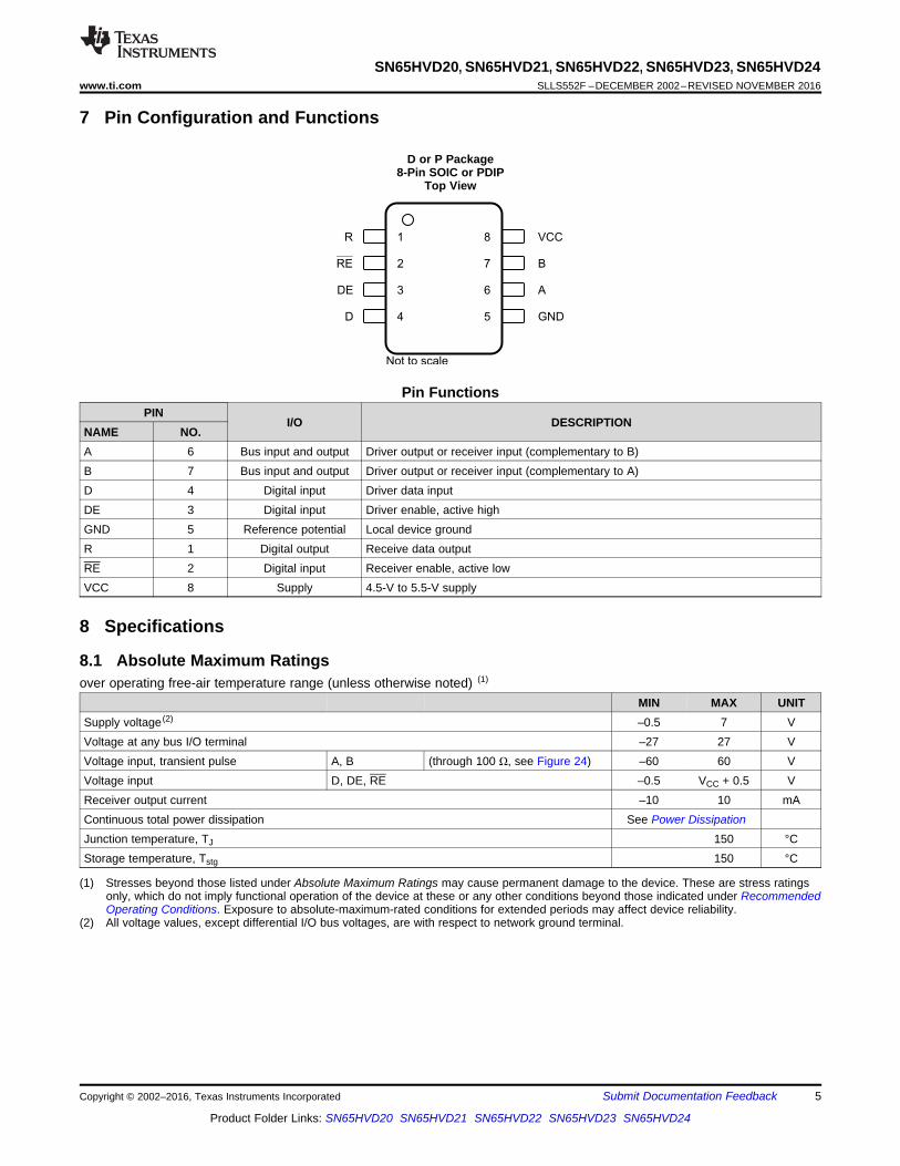
7 Pin Configuration and Functions
D or P Package8-Pin SOIC or PDIP
Top View
Pin FunctionsPIN
I/O DESCRIPTIONNAME NO.A 6 Bus input and output Driver output or receiver input (complementary to B)B 7 Bus input and output Driver output or receiver input (complementary to A)D 4 Digital input Driver data inputDE 3 Digital input Driver enable, active highGND 5 Reference potential Local device groundR 1 Digital output Receive data outputRE 2 Digital input Receiver enable, active lowVCC 8 Supply 4.5-V to 5.5-V supply
(1) Stresses beyond those listed under Absolute Maximum Ratings may cause permanent damage to the device. These are stress ratingsonly, which do not imply functional operation of the device at these or any other conditions beyond those indicated under RecommendedOperating Conditions. Exposure to absolute-maximum-rated conditions for extended periods may affect device reliability.
(2) All voltage values, except differential I/O bus voltages, are with respect to network ground terminal.
8 Specifications
8.1 Absolute Maximum Ratingsover operating free-air temperature range (unless otherwise noted) (1)
MIN MAX UNITSupply voltage (2) –0.5 7 VVoltage at any bus I/O terminal –27 27 VVoltage input, transient pulse A, B (through 100 Ω, see Figure 24) –60 60 VVoltage input D, DE, RE –0.5 VCC + 0.5 VReceiver output current –10 10 mAContinuous total power dissipation See Power DissipationJunction temperature, TJ 150 °CStorage temperature, Tstg 150 °C

6
SN65HVD20, SN65HVD21, SN65HVD22, SN65HVD23, SN65HVD24SLLS552F –DECEMBER 2002–REVISED NOVEMBER 2016 www.ti.com
Product Folder Links: SN65HVD20 SN65HVD21 SN65HVD22 SN65HVD23 SN65HVD24
Submit Documentation Feedback Copyright © 2002–2016, Texas Instruments Incorporated
(1) Tested in accordance with JEDEC Standard 22, Test Method A114-A.(2) Tested in accordance with JEDEC Standard 22, Test Method C101.(3) Tested in accordance with JEDEC Standard 22, Test Method A115-A
8.2 ESD RatingsVALUE UNIT
V(ESD) Electrostatic discharge
Human-body model (HBM), perANSI/ESDA/JEDEC JS-001 (1)
All pins except 5, 6, and 7 ±5000
VPins 5, 6, and 7 ±16000
Charged-device model (CDM), per JEDEC specification JESD22-C101 (2) ±1500Machine Model (MM) (3) ±200
(1) Maximum free-air temperature operation is allowed as long as the device recommended junction temperature is not exceeded.
8.3 Recommended Operating ConditionsMIN NOM MAX UNIT
VCC Supply voltage 4.5 5 5.5 VVoltage at any bus I/O terminal A, B –20 25 V
VIH High-level input voltageD, DE, RE
2 VCC VVIL Low-level input voltage 0 0.8 VVID Differential input voltage A with respect to B –25 25 V
Output currentDriver –110 110
mAReceiver –8 8
ICC Supply current
Driver enabled (DE at VCC),Receiver enabled (RE at 0 V), No load,VI = 0 V or VCC
SN65HVD20 6 9
mA
SN65HVD21 8 12SN65HVD22 6 9SN65HVD23 7 11SN65HVD24 10 14
Driver enabled (DE at VCC),Receiver disabled (RE at VCC), No load,VI = 0 V or VCC
SN65HVD20 5 8SN65HVD21 7 11SN65HVD22 5 8SN65HVD23 5 9SN65HVD24 8 12
Driver disabled (DE at 0 V),Receiver enabled (RE at 0 V), No load
SN65HVD20 4 7SN65HVD21 5 8SN65HVD22 4 7SN65HVD23 4.5 9SN65HVD24 5.5 10
Driver disabled (DE at 0 V), Receiverdisabled (RE at VCC) D open All SN65HVD2x 1 µA
TA Operating free-air temperature (1) –40 85 °CTJ Junction temperature –40 130 °C

7
SN65HVD20, SN65HVD21, SN65HVD22, SN65HVD23, SN65HVD24www.ti.com SLLS552F –DECEMBER 2002–REVISED NOVEMBER 2016
Product Folder Links: SN65HVD20 SN65HVD21 SN65HVD22 SN65HVD23 SN65HVD24
Submit Documentation FeedbackCopyright © 2002–2016, Texas Instruments Incorporated
(1) For more information about traditional and new thermal metrics, see the Semiconductor and IC Package Thermal Metrics applicationreport.
8.4 Thermal Information
THERMAL METRIC (1)SN65HVD2x
UNITD (SOIC) P (PDIP)8 PINS 8 PINS
RθJA Junction-to-ambient thermal resistance 78.1 52.5 °C/WRθJC(top) Junction-to-case(top) thermal resistance 56.5 57.6 °C/WRθJB Junction-to-board thermal resistance 50.4 38.6 °C/WψJT Junction-to-top characterization parameter 4.1 19.1 °C/WψJB Junction-to-board characterization parameter 32.6 31.9 °C/W
(1) All typical values are at VCC = 5 V and 25°C.
8.5 Driver Electrical Characteristicsover recommended operating conditions (unless otherwise noted). (1)
PARAMETER TEST CONDITIONS MIN TYP MAX UNIT
VIK Input clamp voltage II = –18 mA –1.5 0.75 V
VO Open-circuit output voltage A or B, No load 0 VCC V
|VOD(SS)| Steady-state differential output voltage
No load (open circuit) 3.3 4.2 VCC
VRL = 54 Ω, See Figure 9 1.8 2.5
With common-mode loading, See Figure 10 1.8
Δ|VOD(SS)|Change in steady-state differential output voltagebetween logic states See Figure 9 and Figure 11 –0.1 0.1 V
VOC(SS) Steady-state common-mode output voltage See Figure 9 2.1 2.5 2.9 V
∆VOC(SS)Change in steady-state common-mode outputvoltage, VOC(H) – VOC(L)
See Figure 9 and Figure 12 –0.1 0.1 V
VOC(PP)Peak-to-peak common-mode output voltage,VOC(MAX) – VOC(MIN)
RL = 54 Ω, CL = 50 pF, See Figure 9 and Figure 12 0.35 V
VOD(RING) Differential output voltage over and under shoot RL = 54 Ω, CL = 50 pF, See Figure 13 10%
II Input current D, DE –100 100 µA
IOOutput current with power off.High impedance state output current.
VO = –7 V to 12 V,Other input = 0 V
SN65HVD2[0,3] –400 500
µASN65HVD2[1,2,4] –100 125
VO = –20 V to 25 V,Other input = 0 V
SN65HVD2[0,3] –800 1000
SN65HVD2[1,2,4] –200 250
IOS Short-circuit output current VO = –20 V to 25 V, See Figure 17 –250 250 mA
COD Differential output capacitance 20 pF

8
SN65HVD20, SN65HVD21, SN65HVD22, SN65HVD23, SN65HVD24SLLS552F –DECEMBER 2002–REVISED NOVEMBER 2016 www.ti.com
Product Folder Links: SN65HVD20 SN65HVD21 SN65HVD22 SN65HVD23 SN65HVD24
Submit Documentation Feedback Copyright © 2002–2016, Texas Instruments Incorporated
(1) All typical values are at VCC = 5 V and 25°C.
8.6 Receiver Electrical Characteristicsover recommended operating conditions (unless otherwise noted) (1)
PARAMETER TEST CONDITIONS MIN TYP MAX UNIT
VIT(+) Positive-going differential input voltage thresholdSee Figure 18
VO = 2.4 V, IO = –8 mA 60 200mV
VIT(–) Negative-going differential input voltage threshold VO = 0.4 V, IO = 8 mA –200 –60
VHYS Hysteresis voltage (VIT+ – VIT–) 100 130 mV
VIT(F+)Positive-going differential input failsafe voltagethreshold See Figure 23
VCM = –7 V to 12 V 40 120 200mV
VCM = –20 V to 25 V 120 250
VIT(F–)Negative-going differential input failsafe voltagethreshold See Figure 23
VCM = –7 V to 12 V –200 –120 –40mV
VCM = –20 V to 25 V –250 –120
VIK Input clamp voltage II = –18 mA –1.5 V
VOH High-level output voltage VID = 200 mV, IOH = –8 mA, See Figure 19 4 V
VOL Low-level output voltage VID = –200 mV, IOL = 8 mA, See Figure 19 0.4 V
II(BUS) Bus input current (power on or power off)
VI = –7 to 12 V,Other input = 0 V
SN65HVD2[0,3] –400 500
µASN65HVD2[1,2,4] –100 125
VI = –20 to 25 V,Other input = 0 V
SN65HVD2[0,3] –800 1000
SN65HVD2[1,2,4] –200 250
II Input current RE –100 100 µA
RI Input resistanceSN65HVD2[0,3] 24
kΩSN65HVD2[1,2,4] 96
CID Differential input capacitance VID = 0.5 + 0.4 sine (2π × 1.5 × 106t) 20 pF
(1) All typical values are at VCC = 5 V and 25°C
8.7 Driver Switching Characteristicsover recommended operating conditions (unless otherwise noted) (1)
PARAMETER TEST CONDITIONS MIN TYP MAX UNIT
tPLH, tPHLDifferential output propagation delay,low-to-high and high-to-low
RL = 54 Ω, CL = 50 pF,See Figure 11
SN65HVD2[0,3] 6 10 20
nsSN65HVD2[1,4] 20 32 60
SN65HVD22 160 280 500
tr, tf Differential output rise time and fall time RL = 54 Ω, CL = 50 pF,See Figure 11
SN65HVD2[0,3] 2 6 12
nsSN65HVD2[1,4] 20 40 60
SN65HVD22 200 400 600
tPZH, tPHZ
Propagation delay time,high-impedance-to-high-level output andhigh-level output-to-high-impedance
RE at 0 V, See Figure 14
SN65HVD2[0,3] 40
nsSN65HVD2[1,4] 100
SN65HVD22 300
tPZL, tPLZ
Propagation delay time,high-impedance-to-high-level output andhigh-level output-to-high-impedance
RE at 0 V, See Figure 15
SN65HVD2[0,3] 40
nsSN65HVD2[1,4] 100
SN65HVD22 300
td(standby) Time from an active differential output to standbyRE at VCC, See Figure 16
2 µs
td(wake)Wake-up time from standby to an active differentialoutput 8 µs
tsk(p) Pulse skew | tPLH – tPHL|
SN65HVD2[0,3] 2
nsSN65HVD2[1,4] 6
SN65HVD22 50

9
SN65HVD20, SN65HVD21, SN65HVD22, SN65HVD23, SN65HVD24www.ti.com SLLS552F –DECEMBER 2002–REVISED NOVEMBER 2016
Product Folder Links: SN65HVD20 SN65HVD21 SN65HVD22 SN65HVD23 SN65HVD24
Submit Documentation FeedbackCopyright © 2002–2016, Texas Instruments Incorporated
8.8 Receiver Switching Characteristicsover recommended operating conditions (unless otherwise noted)
PARAMETER TEST CONDITIONS MIN TYP MAX UNIT
tPLH Propagation delay time,low-to-high level output andhigh-to low level output
See Figure 19SN65HVD2[0,3] 16 35 ns
tPHL SN65HVD2[1,2,4] 25 50
trtf
Receiver output rise timeReceiver output fall time See Figure 19 2 4 ns
tPZH Receiver output enable time to high level anddisable time from high level See Figure 20
90 120ns
tPHZ 16 35
tPZL Receiver output enable time to low level anddisable time from low level See Figure 21
90 120ns
tPLZ 16 35
tr(standby) Time from an active receiver output to standby See Figure 22, DE at 0 V 2 µs
tr(wake)Wake-up time from standby to an active receiveroutput See Figure 22, DE at 0 V 8 µs
tsk(p) Pulse skew |tPLH – tPHL| 5 ns
tp(set) Delay time, bus fail to failsafe set See Figure 23, pulse rate = 1 kHz 250 350 µs
tp(reset) Delay time, bus recovery to failsafe reset See Figure 23, pulse rate = 1 kHz 50 ns
(1) The SN65HVD20 and SN65HVD21 do not have receiver equalization, but are specified for comparison.(2) All typical values are at VCC = 5 V, and temperature = 25°C.
8.9 Receiver Equalization Characteristics (1)
over recommended operating conditions (unless otherwise noted) (2)
PARAMETER TEST CONDITIONS TYP UNIT
tj(pp) Peak-to-peak eye-pattern jitter
Peudo-random NRZ code with abit pattern length of 216 – 1,Beldon 3105A cable,See Figure 26
25 Mbps
0 m SN65HVD23 2 ns
100 mSN65HVD20 6
nsSN65HVD23 3
150 mSN65HVD20 15
nsSN65HVD23 4
200 mSN65HVD20 27
nsSN65HVD23 8
10 Mbps
200 mSN65HVD20 22
nsSN65HVD23 8
250 mSN65HVD20 34
nsSN65HVD23 15
300 mSN65HVD20 49
nsSN65HVD23 27
5 Mbps 500 mSN65HVD21 128
nsSN65HVD24 18
3 Mbps 500 m
SN65HVD20 93
nsSN65HVD21 103SN65HVD23 90SN65HVD24 16
1 Mbps 1000 mSN65HVD21 216
nsSN65HVD24 62

10
SN65HVD20, SN65HVD21, SN65HVD22, SN65HVD23, SN65HVD24SLLS552F –DECEMBER 2002–REVISED NOVEMBER 2016 www.ti.com
Product Folder Links: SN65HVD20 SN65HVD21 SN65HVD22 SN65HVD23 SN65HVD24
Submit Documentation Feedback Copyright © 2002–2016, Texas Instruments Incorporated
8.10 Power DissipationPARAMETERS TEST CONDITIONS VALUE UNIT
PD Device power dissipation
Typical
VCC = 5 V, TJ = 25°C,RL = 54 Ω, CL = 50 pF (driver),CL = 15 pF (receiver),50% Duty cycle square-wave signal,Driver and receiver enabled
SN65HVD20: 25 Mbps 295
mWSN65HVD21: 5 Mbps 260SN65HVD22: 500 kbps 233SN65HVD23: 25 Mbps 302SN65HVD24: 5 Mbps 267
Worstcase
VCC = 5.5 V, TJ = 125°C,RL = 54 Ω, CL = 50 pF,CL = 15 pF (receiver),50% Duty cycle square-wave signal,Driver and receiver enabled
SN65HVD20: 25 Mbps 408
mWSN65HVD21: 5 Mbps 342SN65HVD22: 500 kbps 300SN65HVD23: 25 Mbps 417SN65HVD24: 5 Mbps 352
TSDThermal shut down junctiontemperature 170 °C

1
0
1
2
3
4
5
6
VCM = 25 V
VCM = 0 V
VCM = 20 V
VCM = 25 V
VCM = 0 V
VCM = 20 V
V - Differential Input Voltage - VID
VIT(-) VIT(+)
V-
Receiv
er
Ou
tpu
t V
olt
ag
e -
VO
-0.2 -0.1 0 0.1 0.20
5
10
15
20
25
30
HVD20 = 25 Mbps
Cable Length - m
HVD23 = 25 Mbps
VCC = 5 V,
TA = 25°C,
VIC = 2.5 V,
Cable: Belden 3105A
100 120 140 160 180 200
Peak-t
o-P
eak J
itte
r -
ns
40
45
50
55
60
65
70
75
HVD22HVD21
HVD20VCC = 5 V,
DE = RE = VCC,
LOAD = 54 Ω, 50 pF
Signaling Rate - Mbps
I-
Su
pp
ly C
urr
en
t -
mA
CC
0.1 1 10 1000
0.5
1
1.5
2
2.5
3
3.5
4
4.5
5
VCC = 5.5 V
VCC = 5 V
VCC = 4.5 V
I - Driver Load Current - mAL
V-
Dri
ver
Dif
fere
nti
al O
utp
ut
Vo
ltag
e -
VO
D
0 10 20 30 40 50 60 70 80
600
400
200
0
200
400
600
VCC = 0 V
VCC = 5 V
Bus Pin Voltage - V
Bu
s P
in C
urr
en
t -
Am
DE = 0 V
-30 -20 -10 0 10 20 30
150
100
50
0
50
100
150
VCC = 0 V
VCC = 5 V
Bu
s P
in C
urr
en
t -
Am
DE = 0 V
Bus Pin Voltage - V
-30 -20 -10 0 10 20 30
11
SN65HVD20, SN65HVD21, SN65HVD22, SN65HVD23, SN65HVD24www.ti.com SLLS552F –DECEMBER 2002–REVISED NOVEMBER 2016
Product Folder Links: SN65HVD20 SN65HVD21 SN65HVD22 SN65HVD23 SN65HVD24
Submit Documentation FeedbackCopyright © 2002–2016, Texas Instruments Incorporated
8.11 Typical Characteristics
Figure 1. SN65HVD2[0,3] Bus Pin Currentvs Bus Pin Voltage
Figure 2. SN65HVD2[1,2,4] Bus Pin Currentvs Bus Pin Voltage
Figure 3. Supply Current vs Signaling Rate Figure 4. Driver Differential Output Voltagevs Driver Load Current
Figure 5. Receiver Output Voltagevs Differential Input Voltage
Figure 6. SN65HVD2[0,3] Peak-to-Peak Jittervs Cable Length

IO
IO
VOD 60 Ω
VTEST
0 V or 3 V
375 Ω
375 Ω
VTEST = -20 V to 25 V
II
IO
IO
VOD 50 pF
27 Ω
27 Ω
VOC
0 V or 3 V
10
30
50
70
90
110
130HVD21: 500 m Cable
Signaling Rate - Mbps
VCC = 5 V,
TA = 25°C,
VIC = 2.5 V,
Cable: Belden 3105A
HVD24: 500 m Cable
Peak-t
o-P
eak J
itte
r -
ns
3 3.5 4 4.5 5
0
10
20
30
40
50
60
70
HVD21 = 10 Mbps
HVD20 = 10 Mbps
HVD23 = 10 Mbps
HVD24 = 10 Mbps
VCC = 5 V,
TA = 25°C,
VIC = 2.5 V,
Cable: Belden 3105A
Cable Length - m
200 220 240 260 280 300
Peak-t
o-P
eak J
itte
r -
ns
12
SN65HVD20, SN65HVD21, SN65HVD22, SN65HVD23, SN65HVD24SLLS552F –DECEMBER 2002–REVISED NOVEMBER 2016 www.ti.com
Product Folder Links: SN65HVD20 SN65HVD21 SN65HVD22 SN65HVD23 SN65HVD24
Submit Documentation Feedback Copyright © 2002–2016, Texas Instruments Incorporated
Typical Characteristics (continued)
Figure 7. SN65HVD2[0,1,3,4] Peak-to-Peak Jittervs Cable Length
Figure 8. SN65HVD2[1,4] Peak-to-Peak Jittervs Signaling Rate
9 Parameter Measurement Information
NOTETest load capacitance includes probe and jig capacitance (unless otherwise specified).Signal generator characteristics: rise and fall time <6 ns, pulse rate 100 kHz, 50% dutycycle, Zo = 50 Ω (unless otherwise specified).
Figure 9. Driver Test Circuit, VOD and VOC Without Common-Mode Loading
Figure 10. Driver Test Circuit, VOD With Common-Mode Loading

50 Ω
CL = 50 pF
Signal
Generator
DE
D0 V or 3 V
3 V if Testing A Output
0 V if Testing B Output
A
B
RL = 110 Ω
OutputS1
tPZH
tPHZ
0.5 V
DE
Output
1.5 V 1.5 V
2.5 V
3 V
0 V
VOH
VOff 0
VOD(PP)
VOD(RING)
VOD(RING)
VOD(SS)
0 V Differential
VOD(SS)
VOC50 Ω
Signal
Generator
A
B
27 Ω
27 Ω
50 pF
DVA
VB
VOC
VOC(PP) ∆VOC(SS)
≈ -3.25 V
≈ -1.75 V
VOD
50 Ω
RL = 54 Ω
CL = 50 pFSignal
Generator
1.5 V 1.5 V
3 V
0 V
tPLH tPHL
VOD(H)
VOD(L)
90%0 V
10%
tr tf
INPUT
OUTPUT
13
SN65HVD20, SN65HVD21, SN65HVD22, SN65HVD23, SN65HVD24www.ti.com SLLS552F –DECEMBER 2002–REVISED NOVEMBER 2016
Product Folder Links: SN65HVD20 SN65HVD21 SN65HVD22 SN65HVD23 SN65HVD24
Submit Documentation FeedbackCopyright © 2002–2016, Texas Instruments Incorporated
Parameter Measurement Information (continued)
Figure 11. Driver Switching Test Circuit and Waveforms
Figure 12. Driver VOC Test Circuit and Waveforms
VOD(RING) is measured at four points on the output waveform, corresponding to overshoot and undershoot from theVOD(H) and VOD(L) steady state values.
Figure 13. VOD(RING) Waveform and Definitions
Figure 14. Driver Enable and Disable Test, High Output

IO
VO
VID
Voltage
Source
IOS
VO
VODRL = 54 ΩCL = 50 pF
50 Ω
Signal
Generator
DE
D0 V or 3 V
A
B
3 V
1.5 V
0 V
0.2 V
1.5 V
td(Wake)td(Standby)
DE
V OD
50 Ω
CL = 50 pF
Signal
Generator
DE
D0 V or 3 V
0 V if Testing A Output
3 V if Testing B Output
RL = 110 Ω
Output
S1
tPZLtPLZ
0.5 V
DE
Output
1.5 V 1.5 V
2.5 V
3 V
0 V
5 V
VOL
5 V
14
SN65HVD20, SN65HVD21, SN65HVD22, SN65HVD23, SN65HVD24SLLS552F –DECEMBER 2002–REVISED NOVEMBER 2016 www.ti.com
Product Folder Links: SN65HVD20 SN65HVD21 SN65HVD22 SN65HVD23 SN65HVD24
Submit Documentation Feedback Copyright © 2002–2016, Texas Instruments Incorporated
Parameter Measurement Information (continued)
Figure 15. Driver Enable and Disable Test, Low Output
Figure 16. Driver Standby and Wake Test Circuit and Waveforms
Figure 17. Driver Short-Circuit Test
Figure 18. Receiver DC Parameter Definitions

50 ΩSignal
Generator
RE
B
A
54 Ω
CL = 15 pF
R 1 kΩ5 V
0 V
VCC
D
DE
RE
R
1.5 V
tPZL tPLZ
3 V
0 V
VCC
VOL +0.5 V1.5 V
VOL
50 Ω
Signal
Generator
RE
B
A
54 Ω
CL = 15 pF
R 1 kΩ0 V
VCC
VCC
D
DE
RE
R
1.5 V
tPZH tPHZ
3 V
0 V
VOH
VOH -0.5 V
GND
1.5 V
50 Ω
Signal
Generator
CL = 15 pF50 Ω
Signal
Generator
A
VID
BR
IO
VO
50%
90%
10%
1.5 V
0 V
VOH
VOL
tPLH tPHL
tr tf
Input B
Input A
Output 1.5 V
15
SN65HVD20, SN65HVD21, SN65HVD22, SN65HVD23, SN65HVD24www.ti.com SLLS552F –DECEMBER 2002–REVISED NOVEMBER 2016
Product Folder Links: SN65HVD20 SN65HVD21 SN65HVD22 SN65HVD23 SN65HVD24
Submit Documentation FeedbackCopyright © 2002–2016, Texas Instruments Incorporated
Parameter Measurement Information (continued)
Figure 19. Receiver Switching Test Circuit and Waveforms
Figure 20. Receiver Enable Test Circuit and Waveforms, Data Output High
Figure 21. Receiver Enable Test Circuit and Waveforms, Data Output Low

Pulse Generator,
15 ms Duration,
1% Duty Cycle
100 ΩVTEST
0 V
15 ms 1.5 ms V TEST
Bus Data Valid Region
Bus Data
Transition Region
Bus Data Valid Region
tp(SET) tp(RESET)
200 mV
-40 mV-200 mV
-1.5 V
VOH
VOL
1.5 V
VID
R
1.5 V
50 Ω
Signal
Generator
RE
B
A
CL = 15 pF
R
1 kΩ
Switch Down for V(A) = 1.5 V,Switch Up for V(A) = -1.5 V
VCC
1.5 V or
-1.5 V
tr(Wake) tr(Standby)
RE
5 V
0 V
1.5 VVOH 0.5 V
VOL +0.5 V
3 V
0 V
VOH
VOL
R
16
SN65HVD20, SN65HVD21, SN65HVD22, SN65HVD23, SN65HVD24SLLS552F –DECEMBER 2002–REVISED NOVEMBER 2016 www.ti.com
Product Folder Links: SN65HVD20 SN65HVD21 SN65HVD22 SN65HVD23 SN65HVD24
Submit Documentation Feedback Copyright © 2002–2016, Texas Instruments Incorporated
Parameter Measurement Information (continued)
Figure 22. Receiver Standby and Wake Test Circuit and Waveforms
Figure 23. Receiver Active Failsafe Definitions and Waveforms
Figure 24. Test Circuit and Waveforms, Transient Overvoltage Test

B
A6
7
R
2
1
RE
DE
D
3
4
ActiveFilters
+
+120 mV
120 mVTimer250 s P
(VA-VB ) : Not High
(VA-V B) : Not LowBus InputInvalid
SlewRate
Control
STANDBY
-
-
Copyright © 2016, Texas Instruments Incorporated
17
SN65HVD20, SN65HVD21, SN65HVD22, SN65HVD23, SN65HVD24www.ti.com SLLS552F –DECEMBER 2002–REVISED NOVEMBER 2016
Product Folder Links: SN65HVD20 SN65HVD21 SN65HVD22 SN65HVD23 SN65HVD24
Submit Documentation FeedbackCopyright © 2002–2016, Texas Instruments Incorporated
10 Detailed Description
10.1 OverviewThe SN65HVD2x family of devices are RS-485 compliant half-duplex transceivers designed for communicationrates up to 500 kbps (SN65HVD22), 3 Mbps (SN65HVD24), 5 Mbps (SN65HVD21), or 25 Mpbs (SN65HVD20and SN65HVD23). The devices feature extended common-mode range support, which provides immunity tolarger ground potential differences that can occur between nodes that communicate over longer distances. TheSN65HVD23 and the SN65HVD24 devices feature receiver equalization, which reduces the amount of data-dependent jitter that is introduced by the high-frequency losses associated with long cables.
10.2 Functional Block Diagram
10.3 Feature Description
The SN65HVD2x family of devices integrates a differential receiver and differential driver with additional featuresfor improved performance in electrically-noisy, long-cable, or other fault-intolerant applications.
The receiver hysteresis (typically 130 mV) is much larger than found in typical RS-485 transceivers. This helpsreject spurious noise signals which would otherwise cause false changes in the receiver output state.
Slew rate limiting on the driver outputs (SN65HVD2[1,2,4]) reduces the high-frequency content of signal edges.This decreases reflections from bus discontinuities, and allows longer stub lengths between nodes and the mainbus line. Designers must consider the maximum signaling rate and cable length required for a specificapplication, and choose the transceiver best matching those requirements.
When DE is low, the differential driver is disabled, and the A and B outputs are in high-impedance states. WhenDE is high, the differential driver is enabled, and drives the A and B outputs according to the state of the Dinputs.
When RE is high, the differential receiver output buffer is disabled, and the R output is in a high-impedance state.When RE is low, the differential receiver is enabled, and the R output reflects the state of the differential businputs on the A and B pins.

H(s) = k0
(1–k )1
k1p
1(1–k )2
k2p
2k
3p
3k0
(DC
loss)
p1
(MHz)k1
p2
(MHz)k2
p3
(MHz)k3
Similar to 160m of Belden 3105A 0.95 0.25 0.3 3.5 0.5 15 1
Similar to 250m of Belden 3105A 0.9 0.25 0.4 3.5 0.7 12 1
Similar to 500m of Belden 3105A 0.8 0.25 0.6 2.2 1 8 1
Similar to 1000m of Belden 3105A 0.6 0.3 1 3 1 6 1
H(s)Signal
Generator
+(s + p )1
+(s + p )2
(1–k )3+
(s + p )3
18
SN65HVD20, SN65HVD21, SN65HVD22, SN65HVD23, SN65HVD24SLLS552F –DECEMBER 2002–REVISED NOVEMBER 2016 www.ti.com
Product Folder Links: SN65HVD20 SN65HVD21 SN65HVD22 SN65HVD23 SN65HVD24
Submit Documentation Feedback Copyright © 2002–2016, Texas Instruments Incorporated
Feature Description (continued)If both the driver and receiver are disabled, (DE low and RE high) then all nonessential circuitry, includingauxiliary functions such as failsafe and receiver equalization is placed in a low-power standby state. This reducespower consumption to less than 5 µW. When either enable input is asserted, the circuitry again becomes active.
In addition to the primary differential receiver, these devices incorporate a set of comparators and logic toimplement an active receiver failsafe feature. These components determine whether the differential bus signal isvalid. Whenever the differential signal is close to zero volts (neither high nor low), a timer initiates, If thedifferential input remains within the transition range for more than 250 µs, the timer expires and set the receiveroutput to the high state. If a valid bus input (high or low) is received at any time, the receiver output reflects thevalid bus state, and the timer is reset.
Figure 25. SN65HVD22 Receiver Operation With 20-V Offset on Input Signal
Figure 26. Cable Attenuation Model for Jitter Measurements

6
7
A
B3
4
2
1
DE
D
RE
R
19
SN65HVD20, SN65HVD21, SN65HVD22, SN65HVD23, SN65HVD24www.ti.com SLLS552F –DECEMBER 2002–REVISED NOVEMBER 2016
Product Folder Links: SN65HVD20 SN65HVD21 SN65HVD22 SN65HVD23 SN65HVD24
Submit Documentation FeedbackCopyright © 2002–2016, Texas Instruments Incorporated
10.4 Device Functional ModesThe driver and receiver behavior for different input conditions are shown in Table 3 and Table 4, respectively.
(1) Legend: H = high level, L = low level, X = don’t care, Z = high impedance (off), ? = indeterminate
Table 3. Driver Function Table (1)
DEVICEINPUT ENABLE OUTPUTS
D DE A B
SN65HVD2[0,1,2]
H H H LL H L HX L Z ZX OPEN Z Z
OPEN H H L
SN65HVD2[3,4]
H H H LL H L HX L Z ZX OPEN Z Z
OPEN H L H
(1) H = high level, L = low level, Z = high impedance (off)(2) If the differential input VID remains within the transition range for
more than 250 µs, the integrated failsafe circuitry detects a bus fault,and set the receiver output to a high state. See Figure 23.
Table 4. Receiver Function Table (1)
DIFFERENTIAL INPUTVID = (VA – VB)
ENABLERE
OUTPUTR
0.2 V ≤ VID L H–0.2 V < VID < 0.2 V L H (2)
VID ≤ –0.2 V L LX H ZX OPEN ZOpen circuit L HShort Circuit L HIdle (terminated) bus L H
Figure 27. Logic Diagram

20
SN65HVD20, SN65HVD21, SN65HVD22, SN65HVD23, SN65HVD24SLLS552F –DECEMBER 2002–REVISED NOVEMBER 2016 www.ti.com
Product Folder Links: SN65HVD20 SN65HVD21 SN65HVD22 SN65HVD23 SN65HVD24
Submit Documentation Feedback Copyright © 2002–2016, Texas Instruments Incorporated
10.4.1 Test Mode Driver DisableIf the input signal to the D pin is such that:1. the signal has signaling rate above 4 Mbps (for the SN65HVD21 and SN65HVD24),2. the signal has signaling rate above 6 Mbps (for the SN65HVD20 and SN65HVD23),3. the signal has average amplitude from 1.2 V to 1.6 V (1.4 V ± 200 mV), or4. the average signal amplitude remains in this range for 100 µs or longer,
then the driver may activate a test-mode during which the driver outputs are temporarily disabled. This can causeloss of transmission of data during the period that the device is in the test-mode. The driver is re-enabled andresumes normal operation whenever the above conditions are not true. The device is not damaged by this testmode.
Although rare, there are combinations of specific voltage levels and input data patterns within the operatingconditions of the SN65HVD2x family which may lead to a temporary state where the driver outputs are disabledfor a period of time.
Observations:1. The conditions for inadvertently entering the test mode are dependent on the levels, duration, and duty cycle
of the logic signal input to the D pin. Operating input levels are specified as greater than 2 V for a logic HIGHinput, and less than 0.8 V for a logic LOW input. Therefore, a valid steady-state logic input does not causethe device to activate the test mode
2. Only input signals with frequency content above 2 MHz (4 Mbps) have a possibility of activating the testmode. Therefore, this issue should not affect the normal operation of the SN65HVD22 (500 kbps).
3. For operating signaling rates of 4 Mbps (or above), the conditions stated above must remain true over aperiod of: 4 Mbps ×100 µs = 400 bits. Therefore, a normal short message does not inadvertently activate thetest model.
4. One example of an input signal which may cause the test mode to activate is a clock signal with frequency 3MHz and 50% duty cycle (symmetric HIGH and LOW half-cycles) with logic HIGH levels of 2.4 V and logicLOW levels of 0.4 V. This signal applied to the D pin as a driver input would meet the criteria listed above,and may cause the test-mode to activate, which would disable the driver. This example situation may occur ifthe clock signal is generated from a microcontroller or logic chip with a 2.7-V supply.

9 V
1 kΩ
100 kΩ
Input
VCC
RE Inputs
9 V
1 kΩ
100 kΩ
Input
VCC
DE Input
29 V
R3R1
R2
Input
A Input
29 V
R3R1
R2
Input
B Input
29 V
VCC
A and B Outputs
9 V
VCC
R Output
5 Ω
Output
VCCVCC
Output
D Inputs (HVD20, 21, 22) D Inputs (HVD23, 24)
29 V
21
SN65HVD20, SN65HVD21, SN65HVD22, SN65HVD23, SN65HVD24www.ti.com SLLS552F –DECEMBER 2002–REVISED NOVEMBER 2016
Product Folder Links: SN65HVD20 SN65HVD21 SN65HVD22 SN65HVD23 SN65HVD24
Submit Documentation FeedbackCopyright © 2002–2016, Texas Instruments Incorporated
10.4.2 Equivalent Input and Output Schematic Diagrams
Figure 28. Equivalent Input and Output Schematic Diagrams
Table 5. Input and Output Resistor ValuesDEVICE R1, R2 R3
SN65HVD2[0,3] 9 kΩ 45 kΩSN65HVD2[1,2,4] 36 kΩ 180 kΩ
R
D
R
RE
DE
D
A
B
R
D
R
RE
DE
D
A
B
R
D
R
RE
DE
D
A
B
Copyright © 2016, Texas Instruments Incorporated
22
SN65HVD20, SN65HVD21, SN65HVD22, SN65HVD23, SN65HVD24SLLS552F –DECEMBER 2002–REVISED NOVEMBER 2016 www.ti.com
Product Folder Links: SN65HVD20 SN65HVD21 SN65HVD22 SN65HVD23 SN65HVD24
Submit Documentation Feedback Copyright © 2002–2016, Texas Instruments Incorporated
11 Application and Implementation
NOTEInformation in the following applications sections is not part of the TI componentspecification, and TI does not warrant its accuracy or completeness. TI’s customers areresponsible for determining suitability of components for their purposes. Customers shouldvalidate and test their design implementation to confirm system functionality.
11.1 Application InformationThe SN65HVD2x devices are half-duplex RS-485 transceivers that can be used for bidirectional, multipointcommunication at various data rates over differential transmission lines. These devices support a wide common-mode range, allowing for robust communication even in the presence of voltage differences between thereference potentials of different nodes on a network.
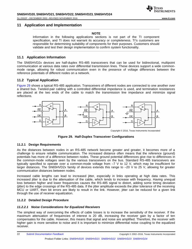
11.2 Typical ApplicationFigure 29 shows a typical RS-485 application. Transceivers of different nodes are connected to one another overa shared bus. Twisted-pair cabling with a controlled differential impedance is used, and termination resistancesare placed at the two ends of the cable to match the transmission line impedance and minimize signalreflections.
Figure 29. Half-Duplex Transceiver Configurations
11.2.1 Design RequirementsAs the distances between nodes in an RS-485 network become greater and greater, it becomes more of achallenge to ensure reliable communication. The increased distance often means that the reference (ground)potentials has more of a difference between nodes. These ground potential differences give rise to differences inthe common-mode voltages seen by the various transceivers on the bus. Standard RS-485 transceivers aretypically specified to operate over a common-mode voltage from –7 V to 12 V, which may be insufficient forlarger distances. The SN65HVD2x family of devices extends this range to –20 V to 25 V, allowing for greatercommunication distances between nodes.
Increased cable lengths can lead to increased jitter, especially in links operating at high data rates. Thisincreased jitter is due to the attenuation of the cable, which tends to increase with frequency. Having unequalloss between higher and lower frequencies causes the RS-485 signal to distort, adding some timing deviation(jitter) to the edge crossings of the RS-485 data. If the jitter amplitude exceeds the jitter tolerance of the receivingMCU or UART, then bit errors are likely to result in the link. However, jitter can be reduced for a given linkthrough the use of receiver equalization.
11.2.2 Detailed Design Procedure
11.2.2.1 Noise Considerations for Equalized ReceiversThe simplest way of overcoming the effects of cable losses is to increase the sensitivity of the receiver. If themaximum attenuation of frequencies of interest is 20 dB, increasing the receiver gain by a factor of tencompensates for the cable. However, this means that signal and noise are amplified. Therefore, the receiver withhigher gain is more sensitive to noise and it is important to minimize differential noise coupling to the equalizedreceiver.

23
SN65HVD20, SN65HVD21, SN65HVD22, SN65HVD23, SN65HVD24www.ti.com SLLS552F –DECEMBER 2002–REVISED NOVEMBER 2016
Product Folder Links: SN65HVD20 SN65HVD21 SN65HVD22 SN65HVD23 SN65HVD24
Submit Documentation FeedbackCopyright © 2002–2016, Texas Instruments Incorporated
Typical Application (continued)Differential noise is crated when conducted or radiated noise energy generates more voltage on one line of thedifferential pair than the other. For this to occur from conducted or electric far-field noise, the impedance toground of the lines must differ.
For noise frequency out to 50 MHz, the input traces can be treated as a lumped capacitance if the receiver isapproximately 10 inches or less from the connector. Therefore, matching impedance of the lines is accomplishedby matching the lumped capacitance of each.
The primary factors that affect the capacitance of a trace are in length, thickness, width, dielectric material,distance from the signal return path, stray capacitance, and proximity to other conductors. It is difficult to matcheach of the variables for each line of the differential pair exactly, but a reasonable effort to do so keeps the linesbalanced and less susceptible to differential noise coupling.
Another source of differential noise is from near-field coupling. In this situation, an assumption of equal noise-source impedance cannot be made as in the far-field. Familiarly known as crosstalk, more energy from a nearbysignal is coupled to one line of the differential pair. Minimization of this differential noise is accomplished bykeeping the signal pair close together and physical separation from high-voltage, high-current, or high-frequencysignals.
In summary, follow these guidelines in board layout for keeping differential noise to a minimum.• Keep the differential input traces short.• Match the length, physical dimensions, and routing of each line of the pair.• Keep the lines close together.• Match components connected to each line.• Separate the inputs from high-voltage, high-frequency, or high-current signals.
11.2.3 Application CurvesFigure 30 illustrates the benefits of integrated receiver equalization as implemented in the SN65HVD23transceiver. In this test setup, a differential signal generator applied a signal voltage at one end of the cable,which was Belden 3105A twisted-pair shielded cable. The test signal was a pseudo-random bit stream (PRBS) ofnonreturn-to-zero (NRZ) data. Channel 1 (top) shows the eye-pattern of the differential voltage at the receiverinputs (after the cable attenuation). Channel 2 (bottom) shows the output of the receiver.
Figure 31 illustrates the benefits of integrated receiver equalization as implemented in the SN65HVD24transceiver. In this test setup, a differential signal generator applied a signal voltage at one end of the cable,which was Belden 3105A twisted-pair shielded cable. The test signal was a pseudo-random bit stream (PRBS) ofnonreturn-to-zero (NRZ) data. Channel 1 (top) shows the eye-pattern of the bit stream. Channel 2 (middle)shows the eye-pattern of the differential voltage at the receiver inputs (after the cable attenuation). Channel 3(bottom) shows the output of the receiver.

24
SN65HVD20, SN65HVD21, SN65HVD22, SN65HVD23, SN65HVD24SLLS552F –DECEMBER 2002–REVISED NOVEMBER 2016 www.ti.com
Product Folder Links: SN65HVD20 SN65HVD21 SN65HVD22 SN65HVD23 SN65HVD24
Submit Documentation Feedback Copyright © 2002–2016, Texas Instruments Incorporated
Typical Application (continued)
Figure 30. SN65HVD23 Receiver Performance at 25 MbpsOver 150 Meter Cable
Figure 31. SN65HVD24 Receiver Performance at 5 MbpsOver 500 Meter Cable
12 Power Supply RecommendationsTo ensure reliable operation at all data rates and supply voltages, each supply must be decoupled with a 100-nFceramic capacitor placed as close to the supply pins as possible. This helps to reduce supply voltage ripplepresent on the outputs of switched-mode power supplies and also helps to compensate for the resistance andinductance of the PCB power planes.
13 Layout
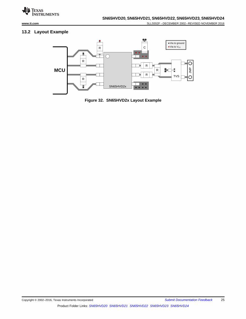
13.1 Layout GuidelinesIn addition to the guidelines on differential trace matching given in Detailed Design Procedure, the layoutguidelines below must be followed:• Route power and ground nets as planes rather than traces, and keep their widths as large as possible to
minimize resistance and inductance while maximizing parasitic capacitance.• If external components (like transient voltage suppression diodes) are used for transient protection, place
them close to the connector port and within the path of the signal lines. Make sure component capacitancesare small enough not to impact the RS-485 signaling at the chosen data rate.
• Small-valued series pulse-proof resistances can be used to provide additional immunity to transients. This isneeded to limit input currents if the clamping voltages of external transient protection devices exceed theabsolute maximum ratings of the transceiver. These resistances must be less than 10 Ω so that the RS-485signal is not overly attenuated.
MCUR
R
Via to ground
SN65HVD2x
JMP
R
R
R
CR Via to VCC
TVS
25
SN65HVD20, SN65HVD21, SN65HVD22, SN65HVD23, SN65HVD24www.ti.com SLLS552F –DECEMBER 2002–REVISED NOVEMBER 2016
Product Folder Links: SN65HVD20 SN65HVD21 SN65HVD22 SN65HVD23 SN65HVD24
Submit Documentation FeedbackCopyright © 2002–2016, Texas Instruments Incorporated
13.2 Layout Example
Figure 32. SN65HVD2x Layout Example

26
SN65HVD20, SN65HVD21, SN65HVD22, SN65HVD23, SN65HVD24SLLS552F –DECEMBER 2002–REVISED NOVEMBER 2016 www.ti.com
Product Folder Links: SN65HVD20 SN65HVD21 SN65HVD22 SN65HVD23 SN65HVD24
Submit Documentation Feedback Copyright © 2002–2016, Texas Instruments Incorporated
14 Device and Documentation Support
14.1 Related LinksThe table below lists quick access links. Categories include technical documents, support and communityresources, tools and software, and quick access to sample or buy.
Table 6. Related Links
PARTS PRODUCT FOLDER SAMPLE & BUY TECHNICALDOCUMENTS
TOOLS &SOFTWARE
SUPPORT &COMMUNITY
SN65HVD20 Click here Click here Click here Click here Click hereSN65HVD21 Click here Click here Click here Click here Click hereSN65HVD22 Click here Click here Click here Click here Click hereSN65HVD23 Click here Click here Click here Click here Click hereSN65HVD24 Click here Click here Click here Click here Click here
14.2 Receiving Notification of Documentation UpdatesTo receive notification of documentation updates, navigate to the device product folder on ti.com. In the upperright corner, click on Alert me to register and receive a weekly digest of any product information that haschanged. For change details, review the revision history included in any revised document.
14.3 Community ResourcesThe following links connect to TI community resources. Linked contents are provided "AS IS" by the respectivecontributors. They do not constitute TI specifications and do not necessarily reflect TI's views; see TI's Terms ofUse.
TI E2E™ Online Community TI's Engineer-to-Engineer (E2E) Community. Created to foster collaborationamong engineers. At e2e.ti.com, you can ask questions, share knowledge, explore ideas and helpsolve problems with fellow engineers.
Design Support TI's Design Support Quickly find helpful E2E forums along with design support tools andcontact information for technical support.
14.4 TrademarksE2E is a trademark of Texas Instruments.All other trademarks are the property of their respective owners.
14.5 Electrostatic Discharge CautionThese devices have limited built-in ESD protection. The leads should be shorted together or the device placed in conductive foamduring storage or handling to prevent electrostatic damage to the MOS gates.
14.6 GlossarySLYZ022 — TI Glossary.
This glossary lists and explains terms, acronyms, and definitions.
15 Mechanical, Packaging, and Orderable InformationThe following pages include mechanical, packaging, and orderable information. This information is the mostcurrent data available for the designated devices. This data is subject to change without notice and revision ofthis document. For browser-based versions of this data sheet, refer to the left-hand navigation.

PACKAGE OPTION ADDENDUM
www.ti.com 18-May-2018
Addendum-Page 1
PACKAGING INFORMATION
Orderable Device Status(1)
Package Type PackageDrawing
Pins PackageQty
Eco Plan(2)
Lead/Ball Finish(6)
MSL Peak Temp(3)
Op Temp (°C) Device Marking(4/5)
Samples
SN65HVD20D ACTIVE SOIC D 8 75 Green (RoHS& no Sb/Br)
CU NIPDAU Level-1-260C-UNLIM -40 to 85 VP20
SN65HVD20DG4 ACTIVE SOIC D 8 75 Green (RoHS& no Sb/Br)
CU NIPDAU Level-1-260C-UNLIM -40 to 85 VP20
SN65HVD20DR ACTIVE SOIC D 8 2500 Green (RoHS& no Sb/Br)
CU NIPDAU Level-1-260C-UNLIM -40 to 85 VP20
SN65HVD20P ACTIVE PDIP P 8 50 Pb-Free(RoHS)
CU NIPDAU N / A for Pkg Type -40 to 85 65HVD20
SN65HVD21D ACTIVE SOIC D 8 75 Green (RoHS& no Sb/Br)
CU NIPDAU Level-1-260C-UNLIM -40 to 85 VP21
SN65HVD21DG4 ACTIVE SOIC D 8 75 Green (RoHS& no Sb/Br)
CU NIPDAU Level-1-260C-UNLIM -40 to 85 VP21
SN65HVD21DR ACTIVE SOIC D 8 2500 Green (RoHS& no Sb/Br)
CU NIPDAU Level-1-260C-UNLIM -40 to 85 VP21
SN65HVD21DRG4 ACTIVE SOIC D 8 2500 Green (RoHS& no Sb/Br)
CU NIPDAU Level-1-260C-UNLIM -40 to 85 VP21
SN65HVD21P ACTIVE PDIP P 8 50 Pb-Free(RoHS)
CU NIPDAU N / A for Pkg Type -40 to 85 65HVD21
SN65HVD21PE4 ACTIVE PDIP P 8 50 Pb-Free(RoHS)
CU NIPDAU N / A for Pkg Type -40 to 85 65HVD21
SN65HVD22D ACTIVE SOIC D 8 75 Green (RoHS& no Sb/Br)
CU NIPDAU Level-1-260C-UNLIM -40 to 85 VP22
SN65HVD22DG4 ACTIVE SOIC D 8 75 Green (RoHS& no Sb/Br)
CU NIPDAU Level-1-260C-UNLIM -40 to 85 VP22
SN65HVD22DR ACTIVE SOIC D 8 2500 Green (RoHS& no Sb/Br)
CU NIPDAU Level-1-260C-UNLIM -40 to 85 VP22
SN65HVD22DRG4 ACTIVE SOIC D 8 2500 Green (RoHS& no Sb/Br)
CU NIPDAU Level-1-260C-UNLIM -40 to 85 VP22
SN65HVD22P ACTIVE PDIP P 8 50 Pb-Free(RoHS)
CU NIPDAU N / A for Pkg Type -40 to 85 65HVD22
SN65HVD22PE4 ACTIVE PDIP P 8 50 Pb-Free(RoHS)
CU NIPDAU N / A for Pkg Type -40 to 85 65HVD22
SN65HVD23D ACTIVE SOIC D 8 75 Green (RoHS& no Sb/Br)
CU NIPDAU Level-1-260C-UNLIM -40 to 85 VP23

PACKAGE OPTION ADDENDUM
www.ti.com 18-May-2018
Addendum-Page 2
Orderable Device Status(1)
Package Type PackageDrawing
Pins PackageQty
Eco Plan(2)
Lead/Ball Finish(6)
MSL Peak Temp(3)
Op Temp (°C) Device Marking(4/5)
Samples
SN65HVD23DG4 ACTIVE SOIC D 8 75 Green (RoHS& no Sb/Br)
CU NIPDAU Level-1-260C-UNLIM -40 to 85 VP23
SN65HVD23DR ACTIVE SOIC D 8 2500 Green (RoHS& no Sb/Br)
CU NIPDAU Level-1-260C-UNLIM -40 to 85 VP23
SN65HVD23DRG4 ACTIVE SOIC D 8 2500 Green (RoHS& no Sb/Br)
CU NIPDAU Level-1-260C-UNLIM -40 to 85 VP23
SN65HVD23P ACTIVE PDIP P 8 50 Pb-Free(RoHS)
CU NIPDAU N / A for Pkg Type -40 to 85 65HVD23
SN65HVD24D ACTIVE SOIC D 8 75 Green (RoHS& no Sb/Br)
CU NIPDAU Level-1-260C-UNLIM -40 to 85 VP24
SN65HVD24DG4 ACTIVE SOIC D 8 75 Green (RoHS& no Sb/Br)
CU NIPDAU Level-1-260C-UNLIM -40 to 85 VP24
SN65HVD24DR ACTIVE SOIC D 8 2500 Green (RoHS& no Sb/Br)
CU NIPDAU Level-1-260C-UNLIM -40 to 85 VP24
SN65HVD24DRG4 ACTIVE SOIC D 8 2500 Green (RoHS& no Sb/Br)
CU NIPDAU Level-1-260C-UNLIM -40 to 85 VP24
(1) The marketing status values are defined as follows:ACTIVE: Product device recommended for new designs.LIFEBUY: TI has announced that the device will be discontinued, and a lifetime-buy period is in effect.NRND: Not recommended for new designs. Device is in production to support existing customers, but TI does not recommend using this part in a new design.PREVIEW: Device has been announced but is not in production. Samples may or may not be available.OBSOLETE: TI has discontinued the production of the device.
(2) RoHS: TI defines "RoHS" to mean semiconductor products that are compliant with the current EU RoHS requirements for all 10 RoHS substances, including the requirement that RoHS substancedo not exceed 0.1% by weight in homogeneous materials. Where designed to be soldered at high temperatures, "RoHS" products are suitable for use in specified lead-free processes. TI mayreference these types of products as "Pb-Free".RoHS Exempt: TI defines "RoHS Exempt" to mean products that contain lead but are compliant with EU RoHS pursuant to a specific EU RoHS exemption.Green: TI defines "Green" to mean the content of Chlorine (Cl) and Bromine (Br) based flame retardants meet JS709B low halogen requirements of <=1000ppm threshold. Antimony trioxide basedflame retardants must also meet the <=1000ppm threshold requirement.
(3) MSL, Peak Temp. - The Moisture Sensitivity Level rating according to the JEDEC industry standard classifications, and peak solder temperature.
(4) There may be additional marking, which relates to the logo, the lot trace code information, or the environmental category on the device.
(5) Multiple Device Markings will be inside parentheses. Only one Device Marking contained in parentheses and separated by a "~" will appear on a device. If a line is indented then it is a continuationof the previous line and the two combined represent the entire Device Marking for that device.

PACKAGE OPTION ADDENDUM
www.ti.com 18-May-2018
Addendum-Page 3
(6) Lead/Ball Finish - Orderable Devices may have multiple material finish options. Finish options are separated by a vertical ruled line. Lead/Ball Finish values may wrap to two lines if the finishvalue exceeds the maximum column width.
Important Information and Disclaimer:The information provided on this page represents TI's knowledge and belief as of the date that it is provided. TI bases its knowledge and belief on informationprovided by third parties, and makes no representation or warranty as to the accuracy of such information. Efforts are underway to better integrate information from third parties. TI has taken andcontinues to take reasonable steps to provide representative and accurate information but may not have conducted destructive testing or chemical analysis on incoming materials and chemicals.TI and TI suppliers consider certain information to be proprietary, and thus CAS numbers and other limited information may not be available for release.
In no event shall TI's liability arising out of such information exceed the total purchase price of the TI part(s) at issue in this document sold by TI to Customer on an annual basis.

TAPE AND REEL INFORMATION
*All dimensions are nominal
Device PackageType
PackageDrawing
Pins SPQ ReelDiameter
(mm)
ReelWidth
W1 (mm)
A0(mm)
B0(mm)
K0(mm)
P1(mm)
W(mm)
Pin1Quadrant
SN65HVD20DR SOIC D 8 2500 330.0 12.4 6.4 5.2 2.1 8.0 12.0 Q1
SN65HVD21DR SOIC D 8 2500 330.0 12.4 6.4 5.2 2.1 8.0 12.0 Q1
SN65HVD22DR SOIC D 8 2500 330.0 12.4 6.4 5.2 2.1 8.0 12.0 Q1
SN65HVD23DR SOIC D 8 2500 330.0 12.4 6.4 5.2 2.1 8.0 12.0 Q1
SN65HVD24DR SOIC D 8 2500 330.0 12.4 6.4 5.2 2.1 8.0 12.0 Q1
PACKAGE MATERIALS INFORMATION
www.ti.com 26-Feb-2016
Pack Materials-Page 1

*All dimensions are nominal
Device Package Type Package Drawing Pins SPQ Length (mm) Width (mm) Height (mm)
SN65HVD20DR SOIC D 8 2500 340.5 338.1 20.6
SN65HVD21DR SOIC D 8 2500 340.5 338.1 20.6
SN65HVD22DR SOIC D 8 2500 340.5 338.1 20.6
SN65HVD23DR SOIC D 8 2500 340.5 338.1 20.6
SN65HVD24DR SOIC D 8 2500 340.5 338.1 20.6
PACKAGE MATERIALS INFORMATION
www.ti.com 26-Feb-2016
Pack Materials-Page 2


IMPORTANT NOTICE
Texas Instruments Incorporated (TI) reserves the right to make corrections, enhancements, improvements and other changes to itssemiconductor products and services per JESD46, latest issue, and to discontinue any product or service per JESD48, latest issue. Buyersshould obtain the latest relevant information before placing orders and should verify that such information is current and complete.TI’s published terms of sale for semiconductor products (http://www.ti.com/sc/docs/stdterms.htm) apply to the sale of packaged integratedcircuit products that TI has qualified and released to market. Additional terms may apply to the use or sale of other types of TI products andservices.Reproduction of significant portions of TI information in TI data sheets is permissible only if reproduction is without alteration and isaccompanied by all associated warranties, conditions, limitations, and notices. TI is not responsible or liable for such reproduceddocumentation. Information of third parties may be subject to additional restrictions. Resale of TI products or services with statementsdifferent from or beyond the parameters stated by TI for that product or service voids all express and any implied warranties for theassociated TI product or service and is an unfair and deceptive business practice. TI is not responsible or liable for any such statements.Buyers and others who are developing systems that incorporate TI products (collectively, “Designers”) understand and agree that Designersremain responsible for using their independent analysis, evaluation and judgment in designing their applications and that Designers havefull and exclusive responsibility to assure the safety of Designers' applications and compliance of their applications (and of all TI productsused in or for Designers’ applications) with all applicable regulations, laws and other applicable requirements. Designer represents that, withrespect to their applications, Designer has all the necessary expertise to create and implement safeguards that (1) anticipate dangerousconsequences of failures, (2) monitor failures and their consequences, and (3) lessen the likelihood of failures that might cause harm andtake appropriate actions. Designer agrees that prior to using or distributing any applications that include TI products, Designer willthoroughly test such applications and the functionality of such TI products as used in such applications.TI’s provision of technical, application or other design advice, quality characterization, reliability data or other services or information,including, but not limited to, reference designs and materials relating to evaluation modules, (collectively, “TI Resources”) are intended toassist designers who are developing applications that incorporate TI products; by downloading, accessing or using TI Resources in anyway, Designer (individually or, if Designer is acting on behalf of a company, Designer’s company) agrees to use any particular TI Resourcesolely for this purpose and subject to the terms of this Notice.TI’s provision of TI Resources does not expand or otherwise alter TI’s applicable published warranties or warranty disclaimers for TIproducts, and no additional obligations or liabilities arise from TI providing such TI Resources. TI reserves the right to make corrections,enhancements, improvements and other changes to its TI Resources. TI has not conducted any testing other than that specificallydescribed in the published documentation for a particular TI Resource.Designer is authorized to use, copy and modify any individual TI Resource only in connection with the development of applications thatinclude the TI product(s) identified in such TI Resource. NO OTHER LICENSE, EXPRESS OR IMPLIED, BY ESTOPPEL OR OTHERWISETO ANY OTHER TI INTELLECTUAL PROPERTY RIGHT, AND NO LICENSE TO ANY TECHNOLOGY OR INTELLECTUAL PROPERTYRIGHT OF TI OR ANY THIRD PARTY IS GRANTED HEREIN, including but not limited to any patent right, copyright, mask work right, orother intellectual property right relating to any combination, machine, or process in which TI products or services are used. Informationregarding or referencing third-party products or services does not constitute a license to use such products or services, or a warranty orendorsement thereof. Use of TI Resources may require a license from a third party under the patents or other intellectual property of thethird party, or a license from TI under the patents or other intellectual property of TI.TI RESOURCES ARE PROVIDED “AS IS” AND WITH ALL FAULTS. TI DISCLAIMS ALL OTHER WARRANTIES ORREPRESENTATIONS, EXPRESS OR IMPLIED, REGARDING RESOURCES OR USE THEREOF, INCLUDING BUT NOT LIMITED TOACCURACY OR COMPLETENESS, TITLE, ANY EPIDEMIC FAILURE WARRANTY AND ANY IMPLIED WARRANTIES OFMERCHANTABILITY, FITNESS FOR A PARTICULAR PURPOSE, AND NON-INFRINGEMENT OF ANY THIRD PARTY INTELLECTUALPROPERTY RIGHTS. TI SHALL NOT BE LIABLE FOR AND SHALL NOT DEFEND OR INDEMNIFY DESIGNER AGAINST ANY CLAIM,INCLUDING BUT NOT LIMITED TO ANY INFRINGEMENT CLAIM THAT RELATES TO OR IS BASED ON ANY COMBINATION OFPRODUCTS EVEN IF DESCRIBED IN TI RESOURCES OR OTHERWISE. IN NO EVENT SHALL TI BE LIABLE FOR ANY ACTUAL,DIRECT, SPECIAL, COLLATERAL, INDIRECT, PUNITIVE, INCIDENTAL, CONSEQUENTIAL OR EXEMPLARY DAMAGES INCONNECTION WITH OR ARISING OUT OF TI RESOURCES OR USE THEREOF, AND REGARDLESS OF WHETHER TI HAS BEENADVISED OF THE POSSIBILITY OF SUCH DAMAGES.Unless TI has explicitly designated an individual product as meeting the requirements of a particular industry standard (e.g., ISO/TS 16949and ISO 26262), TI is not responsible for any failure to meet such industry standard requirements.Where TI specifically promotes products as facilitating functional safety or as compliant with industry functional safety standards, suchproducts are intended to help enable customers to design and create their own applications that meet applicable functional safety standardsand requirements. Using products in an application does not by itself establish any safety features in the application. Designers mustensure compliance with safety-related requirements and standards applicable to their applications. Designer may not use any TI products inlife-critical medical equipment unless authorized officers of the parties have executed a special contract specifically governing such use.Life-critical medical equipment is medical equipment where failure of such equipment would cause serious bodily injury or death (e.g., lifesupport, pacemakers, defibrillators, heart pumps, neurostimulators, and implantables). Such equipment includes, without limitation, allmedical devices identified by the U.S. Food and Drug Administration as Class III devices and equivalent classifications outside the U.S.TI may expressly designate certain products as completing a particular qualification (e.g., Q100, Military Grade, or Enhanced Product).Designers agree that it has the necessary expertise to select the product with the appropriate qualification designation for their applicationsand that proper product selection is at Designers’ own risk. Designers are solely responsible for compliance with all legal and regulatoryrequirements in connection with such selection.Designer will fully indemnify TI and its representatives against any damages, costs, losses, and/or liabilities arising out of Designer’s non-compliance with the terms and provisions of this Notice.
Mailing Address: Texas Instruments, Post Office Box 655303, Dallas, Texas 75265Copyright © 2018, Texas Instruments Incorporated