sol-gel prepared ferroelectric lead-free ...powder metallurgy progress, vol.10 (2010), no 3 169...
TRANSCRIPT

Powder Metallurgy Progress, Vol.10 (2010), No 3 169
SOL-GEL PREPARED FERROELECTRIC LEAD-FREE KNBO3 AND NaNBO3 THIN FILMS AND THEIR MICROSTRUCTURE
H. Bruncková, Ľ. Medvecký, J. Ďurišin
Abstract Environmental acceptable lead-free ferroelectric KNbO3 (KN) or NaNbO3 (NN) thin films were prepared by the modified sol-gel method using the mixing of K or Na acetate with the polymeric Nb-tartarate complex at 80°C and deposited by spin-coating method on Pt/Al2O3 and Pt/SiO2/Si substrates. In the KN or NN thin films, the required perovskite KNbO3 or NaNbO3 phase (on both substrates) and the additional secondary pyrochlore K4Nb6O17 (on both substrates) or Na2Nb8O21 (on Pt/Al2O3) phases were revealed after sintering at 650°C. The surface morphology and thin cross-section of films were investigated by SEM analyses. In the microstructure of 2-layered KN or NN thin films with 100 nm of thickness on Pt/Al2O3 substrate, bimodal particle distribution was observed with the sub-micron sized (around 100 nm) cuboidal particles coalesced to the form of coarser particle clusters (KN) or large clusters (composed of fine particles ~ 30 nm) and coarser rectangular particles (~ 100-200 nm) with microporores about 100-200 nm (NN). The different surface microstructures and cross-section micrographs of 2-layered KN and NN thin films deposited on Pt/SiO2/Si substrate were observed. The large compact clusters (composed of fine particles ~ 30 nm) and coarser rectangular particles ( ~ 100-200 nm) with the microporores ~ 100-200 nm (KN) or bigger needle-like particles (up to 1 μm) representing agglomerates of smaller spherical particles ( ~ 50 nm) were surrounded by a fine cuboidal about 100 nm particles (NN). Keywords: sol-gel, ferroelectric, KNbO3, NaNbO3 thin films, spin-coating, pyrochlore, perovskite phase
INTRODUCTION Alkaline niobates such as the potassium (KNbO3, KN) and sodium (NaNbO3, NN)
thin films have attracted much scientific attention for their excellent nonlinear optical, ferroelectric, piezoelectric, electro-optic ionic conductive, pyroelectric, photorefractive and photocatalytic properties [1,2]. The environment-friendly lead-free ferroelectric (K0.5Na0.5)NbO3 (KNN) thin films with perovskite phase introduce a progressive technological contribution for their dielectric, electrooptic and piezoelectric properties, enabling one to minimize sensors, actuators and scanners of micro-electro-mechanical systems (MEMS) [3].
The physical and chemical methods of thin film preparation onto different substrates are known: sputtering, pulsed laser deposition (PLD), physical vapour deposition (PVD), chemical vapour deposition (CVD) and chemical solution deposition (CSD, sol-gel) [4,5,6]. The advantages of sol-gel process are: stoichiometry control, homogeneity, low process
Helena Bruncková, Ľubomír Medvecký, Juraj Ďurišin, Institute of Materials Research, Slovak Academy of Sciences, Košice, Slovak Republic

Powder Metallurgy Progress, Vol.10 (2010), No 3 170 temperature and low cost. Among the methods of deposition of single film layers in sol form there could be included the following: spin-coating, dip-coating, and electrophoretic deposition (EPD). Included in the different types of synthesis by sol-gel process are: alkoxide (generally using alkoxides), the polymeric complex (PC) Pechini process (generally using oxides, carbonates acetates…) and the modified Pechini methods. In the sol-gel Pechini method, the citric-acid- based Nb and Ta precursors are highly stable polymerizable complexes for the preparation of KNN or Y3NbOy and LiTaO3 synthesis [7]. The sol-gel method offers an approach of depositing thin films with thickness (~ 150-800 nm) on different substrates from sols at temperatures lower than in the conventional alkoxide process. For the preparation of 1-4 layered films, it is necessary to provide multiple repeating of depositing in order to obtain a film of desired thickness and quality [8,9]. Environmentally-acceptable PC synthesis of polymeric Nb-complex is based on interaction of Nb2O5.nH2O (precipitated with NH3 (aq)) disolved in citric acid and ethylene glycol at a certain mole ratio and it is an alternative to the alkoxide method (Nb ethoxide in 2-methoxyethanol). During the sol-gel modified process in dependence upon the type of the interaction between starting components (K2CO3 and Na2CO3) and Nb-complex, solvent (acetic acid) and stabilizer (n-propanol), amorphous film with metastable pyrochlore (py) phase already originates at the calcining temperature of 300-400°C, where pyrolysis of organic compounds into inorganic oxides K2O, Na2O and Nb2O5 occurs [3]. Perovskite (pv) phase forms during sintering at 500-700°C. For crack-free film preparation, it is important to optimize sol concentration and viscosity, spin speed, rotation time and nature substrate. Development of the 1-4 layered thin film microstructure depends on the phase transformation of sol into metastable pyrochlore (py) interphase at film-substrate interface [7].
The present paper describes the sol-gel modified process of the film preparation using polymeric Nb-tartarate complex and the microstructure formation of 2-layered KN and NN thin films deposited from sols on the Pt/Al2O3 and Pt/SiO2/Si substrates by spin-coating method and sintered at 650°C.
EXPERIMENTAL Polymeric Nb-ethylene-glycol-tartarate complex for the KN and NN film synthesis
was prepared by the sol-gel modified method [10]. The niobium (V) chloride was dissolved in ethanol and precipitated with NH3 (aq) to prepare hydrated niobium oxide. The Nb-tartarate-ethylene glycol complex was formed by a reaction of Nb2O5.xH2O with tartaric acid (TA) and H2O2. The obtained solution was dried at 80°C and dissolved in ethylene glycol (EG) (the molar ratio of EG/TA = 5.5).
KN and NN precursors (sols) were synthesized by the sol-gel modified method - mixing K or Na carbonates (alternative of the alkoxides) in acetic acid solution with the Nb-ethylene glycol-tartarate complex at a mole ratio of K or Na:Nb = 1.0 or 1.0:1.0 and temperature of 80°C (see scheme in Fig.1). Basic KN or NN sols were diluted with stabilizer solution (n-propanol : 1,2-propandiol in mole ratio equaling 10:1) to 1.0 M concentration. The resulting sols were transparent and remained stable at room temperature for two months. Two different substrate types - platinized alumina and silicon to deposit the films were applied. Al2O3 polycrystalline wafers or the oxidized p-type silicon [100] single-crystal wafers were used as substrates with a Pt (50 nm) electrode layer (sputtered as a bottom electrode). The SiO2 (250 nm) layers were present between Pt and Si. Pt/Al2O3 and Pt/SiO2/Si substrates were spin-coated with the sol precursor at 2000 rpm for 30s followed by calcining at 400°C for 3 min. The coating-pyrolysis process cycle was repeated twice to obtain 2-layered thin films. Finally, the films were crystallized via sintering at 650°C for 1 hour in air to form the perovskite structure in KN or NN thin films.

Powder Metallurgy Progress, Vol.10 (2010), No 3 171
Fig.1. Scheme of sol-gel method preparation of KN or NN thin films.
The phase composition of KN and NN film was determined by X-ray diffraction analysis (XRD) using CuKα radiation. The microstructures of 1-2 layers KN and NN thin films were characterized using a scanning electron microscope (SEM, Jeol-JSM-7000F) equipped with an energy dispersive X-ray (EDX) analyzer.
RESULTS AND DISCUSSION The 2-layered KN and NN thin films were prepared from sols derived by modified
sol-gel method, deposited on Pt/Al2O3 and Pt/SiO2/Si substrates and sintered at 650°C. XRD diffractograms of 2-layered KN and NN thin films deposited on Pt/Al2O3 and annealed at 650°C (Fig.2) verified the formation of perovskite (pv) KNbO3 (PDF4 00-009-0156) and NaNbO3 (PDF4 00-014-0603) phases. The additional secondary pyrochlore phases were found in the patterns - K4Nb6O17 (PDF4 00-014-0287) and Na2Nb8O21 (PDF4 00-013-0329 + PDF4 00-030-1229). Note that the crystallinity mainly of the secondary phases was very low and it is complicated and practically impossible to do a correct

Powder Metallurgy Progress, Vol.10 (2010), No 3 172 quantitative analysis of the phase composition in both films. Moreover, there can not be excluded some degree of preferential growth of individual particles in films.
Fig.2. XRD diffractograms of the 2-layered KN (bottom) and NN (upper) thin films
deposited on Pt/Al2O3 substrates after sintering at 650°C (x - perovskite KNbO3 (bottom) or NaNbO3 (upper) phase, ● - pyrochlore K4Nb6O17 or - Na2Nb8O21 phase and s -
Pt/Al2O3 substrate).
The XRD diffractograms of 2-layered KN and NN thin films deposited on Pt/SiO2/Si substrates and prepared at 650°C are shown in Fig.3 and Fig.4, respectively. XRD analyses verified formation of the perovskite KNbO3 (PDF4 00-009-0156) phase and pyrochlore K4Nb6O17 (PDF4 00-014-0287 + PDF4 00-021-1295) phase (Fig.3) or pure perovskite NaNbO3 (PDF4 00-014-0603) phase (Fig.4).
Fig.3. XRD diffractogram of the 2-layered KN thin film deposited on Pt/SiO2/Si substrate after sintering at 650°C (× - perovskite KNbO3 phase, ο - pyrochlore K4Nb6O17.3H2O or ●
- K4Nb6O17 phase and s - Pt/SiO2/Si substrate).
Powder Metallurgy Progress, Vol.10 (2010), No 3 173
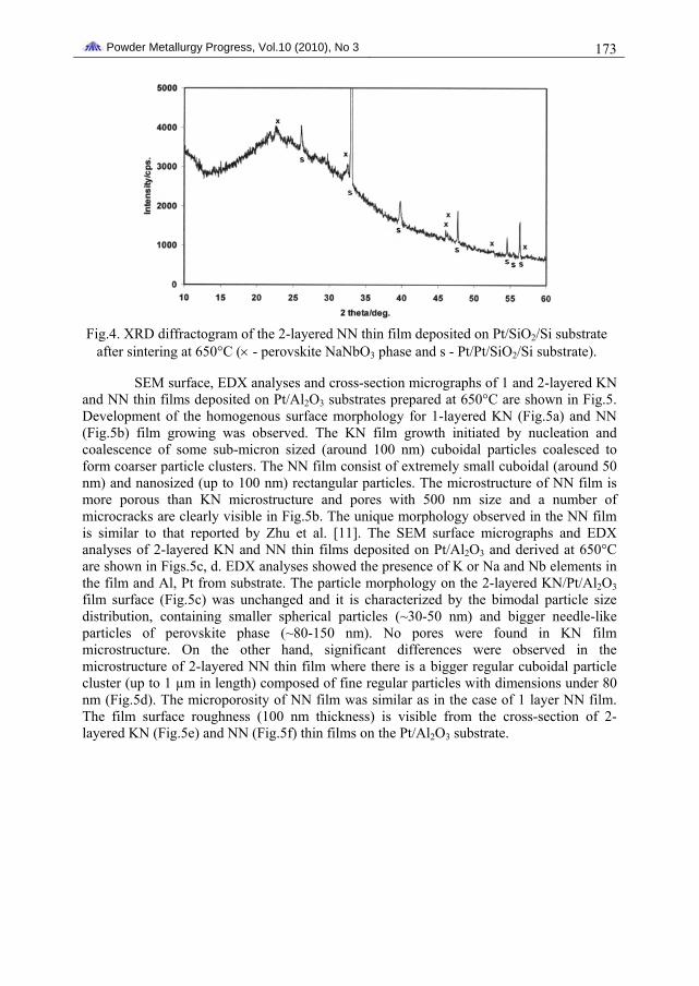
Fig.4. XRD diffractogram of the 2-layered NN thin film deposited on Pt/SiO2/Si substrate
after sintering at 650°C (× - perovskite NaNbO3 phase and s - Pt/Pt/SiO2/Si substrate).
SEM surface, EDX analyses and cross-section micrographs of 1 and 2-layered KN and NN thin films deposited on Pt/Al2O3 substrates prepared at 650°C are shown in Fig.5. Development of the homogenous surface morphology for 1-layered KN (Fig.5a) and NN (Fig.5b) film growing was observed. The KN film growth initiated by nucleation and coalescence of some sub-micron sized (around 100 nm) cuboidal particles coalesced to form coarser particle clusters. The NN film consist of extremely small cuboidal (around 50 nm) and nanosized (up to 100 nm) rectangular particles. The microstructure of NN film is more porous than KN microstructure and pores with 500 nm size and a number of microcracks are clearly visible in Fig.5b. The unique morphology observed in the NN film is similar to that reported by Zhu et al. [11]. The SEM surface micrographs and EDX analyses of 2-layered KN and NN thin films deposited on Pt/Al2O3 and derived at 650°C are shown in Figs.5c, d. EDX analyses showed the presence of K or Na and Nb elements in the film and Al, Pt from substrate. The particle morphology on the 2-layered KN/Pt/Al2O3 film surface (Fig.5c) was unchanged and it is characterized by the bimodal particle size distribution, containing smaller spherical particles (~30-50 nm) and bigger needle-like particles of perovskite phase (~80-150 nm). No pores were found in KN film microstructure. On the other hand, significant differences were observed in the microstructure of 2-layered NN thin film where there is a bigger regular cuboidal particle cluster (up to 1 µm in length) composed of fine regular particles with dimensions under 80 nm (Fig.5d). The microporosity of NN film was similar as in the case of 1 layer NN film. The film surface roughness (100 nm thickness) is visible from the cross-section of 2-layered KN (Fig.5e) and NN (Fig.5f) thin films on the Pt/Al2O3 substrate.

Powder Metallurgy Progress, Vol.10 (2010), No 3 174
Fig.5. SEM surface micrographs of 1-layered thin films (a) KN, (b), NN, EDX analyse
micrographs of 2-layered films (c) KN, (d) NN and cross-section micrographs of 2-layered films (e) KN and (f) NN films deposited on Pt/Al2O3 substrates after sintering at 650°C.
The different surface microstructure and cross-section micrographs of 2-layered KN and NN thin films deposited on Pt/SiO2/Si substrate after sintering at 650°C are shown in Fig.6. KN/Pt/SiO2/Si thin films (Fig.6a) have heterogeneous microstructure, in which two different particle forms can be found: large compact particle clusters (composed of fine particles ~ 30 nm) and coarser rectangular particles (~ 100-200 nm). In comparison with the KN film microstructure formed on Pt/Al2O3 substrate, the micropores with a size in the range of 100-200 nm are created between rectangular particles as the result of particle
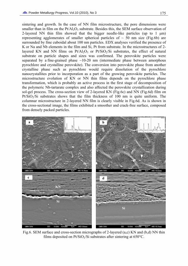
Powder Metallurgy Progress, Vol.10 (2010), No 3 175 sintering and growth. In the case of NN film microstructure, the pore dimensions were smaller than in film on the Pt/Al2O3 substrate. Besides this, the SEM surface observation of 2-layered NN thin film showed that the bigger needle-like particles (up to 1 μm) representing agglomerates of smaller spherical particles of ~ 50 nm size (Fig.6b) are surrounded by fine cuboidal about 100 nm particles. EDX analyses verified the presence of K or Na and Nb elements in the film and Si, Pt from substrate. In the microstructures of 2-layered KN and NN films on Pt/Al2O3 or Pt/SiO2/Si substrates, the effect of natural substrate on particle shapes and sizes was confirmed. The perovskite particles were separated by a fine-grained phase ~10-20 nm (intermediate phase between amorphous pyrochlore and crystalline perovskite). The conversion into perovskite phase from another crystalline phase such as pyrochlore would require dissolution of the pyrochlore nanocrystallites prior to incorporation as a part of the growing perovskite particles. The microstructure evolution of KN or NN thin films depends on the pyrochlore phase transformation, which is probably an active process in the first stage of decomposition of the polymeric Nb-tartarate complex and also affected the perovskite crystallization during sol-gel process. The cross-section view of 2-layered KN (Fig.6c) and NN (Fig.6d) film on Pt/SiO2/Si substrates shows that the film thickness of 100 nm is quite uniform. The columnar microstructure in 2-layered NN film is clearly visible in Fig.6d. As is shown in the cross-sectional image, the films exhibited a smoother and crack-free surface, composed from densely packed particles.
Fig.6. SEM surface and cross-section micrographs of 2-layered (a,c) KN and (b,d) NN thin
films deposited on Pt/SiO2/Si substrates after sintering at 650°C.

Powder Metallurgy Progress, Vol.10 (2010), No 3 176
CONCLUSIONS Lead-free ferroelectric 2-layered KNbO3 (KN) and NaNbO3 (NN) thin films were
prepared using modified sol-gel method from sols, which were deposited by spin-coating method on Pt/Al2O3 and Pt/SiO2/Si substrates and sintered at 650°C.
From the XRD diffractograms it resulted that the required perovskite KNbO3 and NaNbO3 phase, respectively (on both substrates) and the additional secondary pyrochlore K4Nb6O17 (on both substrates) or Na2Nb8O21 phase (on Pt/Al2O3) were formed in KN and NN films.
In the surface microstructures of KN and NN thin films, particles of the perovskite phase were observed and the cross-section thickness of two layers was ~100 nm. In the microstructures of 2-layered KN and NN film, the effect of the substrate nature on particle shapes and sizes was clearly observed. NN film microstructure contained a significant number of micropores which were not observed in KN film. Similarly, particle morphology in NN thin film differs from the one in KN film - the presence of regular particle clusters (~ 1 μm) in NN film. Microstructures of NN and KN thin films on Pt/SiO2/Si substrates were smoother and contained finer particles than ones on Pt/Al2O3 substrates.
Sol-gel method preparation of thin films promotes crystallization at lower temperatures with dense surfaces. Further work will determine the microstructure influence on physical, mechanical and dielectric properties of the prepared KN and NN thin films.
Acknowledgements This work was supported by the Grant Agency of the Slovak Academy of Sciences
through project No. 2/0024/11.
REFERENCES [1] Weber, IT., Garel, M., Bouquet, V., Rousseau, A., Guilloux-Viry, M., Longo, E.,
Perrin, A.: Thin Solid Films, vol. 493, 2005, p. 139 [2] Wu, SY., Liu, XQ., Chen, XM.: Ceram. Int., vol. 36, 2010, p. 871 [3] Söderlind, F., Käll, F., Helmersson, U.: J. Crystal Growth, vol. 281, 2005, p. 468 [4] Li, G., Kako, T., Wang, D., Zou, Z., Ye, J.: J. Phys. Chem. Solids, vol. 69, 2008, p.
2487 [5] Weber, IT., Rousseau, A., Guilloux-Viry, M., Bouquet, V., Perrin, A.: Solid State Sci.,
vol. 7, 2005, p. 1317 [6] Ohno, T., Fujimoto, M., Ota, T., Fuji, M., Takahashi, M., Suzuki, H.: J. Eur. Ceram.
Soc., vol. 26, 2006, p. 2143 [7] Tanaka, K., Kakimoto, K., Ohsato, H.: J. Eur. Ceram. Soc., vol. 27, 2007, p. 3591 [8] Schroeter, C., Wessler, B., Eng, LM.: J. Eur. Ceram. Soc., vol. 27, 2007, p. 3785 [9] Cho, CR.: Mater. Letters, vol. 57, 2002, p. 781
[10] Bruncková, H., Medvecký, Ľ., Mihalik, J.: J. Eur. Ceram. Soc., vol. 28, 2008, p. 123 [11] Zhu, H., Zheng, Z., Gao, X., Huang, Y., Yaan, Z., Zou, J., Zhao, J., Xi, Y., Frost, R.: J.
Am. Chem. Soc., vol. 128, 2006, p. 12