sparse matrix sparse vector multiplication using parallel...
TRANSCRIPT

Sparse Matrix Sparse Vector Multiplication using Parallel and Reconfigurable Computing
A Thesis Presented for the Master of Science
Degree The University of Tennessee
Kirk Andrew Baugher May 2004

Dedication
This thesis is dedicated to my loving wife and our families for their motivation
and support, which has inspired me to push my goals higher and obtain them.
ii

Acknowledgements
I wish to thank all of those who have helped me along my journey of completing
my Master of Science degree in Electrical Engineering. I would especially like to thank
Dr. Peterson for his patience, guidance, wisdom, and support for me in obtaining my
degree. I would like to thank Dr. Bouldin for exposing me to microelectronic design and
for serving on my committee. I would also like to thank Dr. Wong for his support and
guidance and also serving on my committee. In thanking Dr. Wong, I wish to also thank
him on behalf of the Joint Institute for Computational Science in Oak Ridge for making
all of this happen by their support through graduate school. Finally, I wish to thank my
peers who have encouraged and helped me make this all possible.
iii
Abstract
The purpose of this thesis is to provide analysis and insight into the
implementation of sparse matrix sparse vector multiplication on a reconfigurable parallel
computing platform. Common implementations of sparse matrix sparse vector
multiplication are completed by unary processors or parallel platforms today. Unary
processor implementations are limited by their sequential solution of the problem while
parallel implementations suffer from communication delays and load balancing issues
when preprocessing techniques are not used or unavailable. By exploiting the
deficiencies in sparse matrix sparse vector multiplication on a typical unary processor as
a strength of parallelism on an Field Programmable Gate Array (FPGA), the potential
performance improvements and tradeoffs for shifting the operation to hardware assisted
implementation will be evaluated. This will simply be accomplished through multiple
collaborating processes designed on an FPGA.
iv
Table of Contents Chapter Page 1 Introduction....................................................................................................................1 2 Background....................................................................................................................4 2.1 Double Precision Floating-Point..............................................................................4 2.2 Sparse Representation..............................................................................................6 2.3 Sparse Matrix Sparse Vector Multiplication............................................................9 2.4 Field Programmable Gate Arrays ..........................................................................11 2.5 Pilchard System .....................................................................................................12 2.6 Computing Platform...............................................................................................13 3 Analysis of Related Work............................................................................................14 3.1 Floating Point Multiplication and Addition on FPGAs .........................................14 3.2 Sparse Matrix Vector Multiplication on FPGAs ...................................................15 3.3 Sparse Matrix Vector Multiplication on a Unary Processor..................................16 3.4 Sparse Matrix Vector Multiplication on Parallel Processors.................................16 3.5 Sparse Matrix and Sparse Matrix Sparse Vector Multiplication ...........................18 4 Design Approach .........................................................................................................19 4.1 Assumptions...........................................................................................................19 4.1.1 Limited IEEE 754 Format Support ..................................................................19 4.1.2 Use of Compressed Row Scheme....................................................................20 4.1.3 Sparse Matrix and Sparse Vectors ...................................................................20 4.1.4 Generic Design Approach................................................................................20 4.1.5 No Pre-Processing............................................................................................21 4.1.6 Addressable Range...........................................................................................21 4.2 Analysis of the Problem.........................................................................................21 4.3 Analysis of Hardware Limitations .........................................................................22 4.4 Partitioning of the Problem....................................................................................25 4.4.1 Transmission of Data .......................................................................................26 4.4.2 Logic Flow.......................................................................................................30 4.4.3 Comparing of Addresses..................................................................................31 4.4.4 Multiply Accumulator......................................................................................32 4.5 FPGA Design .........................................................................................................33 4.5.1 Pilchard System Interface ................................................................................37 4.5.2 State Machine...................................................................................................40 4.5.3 Comparators.....................................................................................................45 4.5.4 Multiply Accumulator Interface ......................................................................51 4.5.5 Double Precision Floating-Point Multiplier and Adder...................................54 4.5.6 C code interface ...............................................................................................57 5 Results ..........................................................................................................................63 5.1 Comparison of Results...........................................................................................63 5.2 Difficulties .............................................................................................................76
v
5.2.1 Pcore Interface .................................................................................................76 5.2.2 Memory and I/O Constraints ...........................................................................77 5.2.3 Logic Glitch .....................................................................................................79 6 Conclusions and Future Work .....................................................................................81 6.1 Hardware Improvements........................................................................................81 6.2 FPGA Architecture Improvement..........................................................................83 6.3 Algorithmic Improvements....................................................................................84 6.4 Future Applications................................................................................................87 6.5 Conclusion .............................................................................................................88 References ..........................................................................................................................91 Appendices.........................................................................................................................94 Vita...................................................................................................................................206
vi

List of Tables Table Page 2.1 Floating-Point Value Range.....................................................................................5
vii
List of Figures Figure Page 2.1 Floating-Point Representation .................................................................................4 2.2 Irregular Sparse Matrix ............................................................................................6 2.3 Structured Sparse Matrix .........................................................................................6 2.4 Sparse Matrix ...........................................................................................................7 2.5 Sparse Vector ...........................................................................................................8 2.6 Sparse Matrix Sparse Vector Multiplication..........................................................10 2.7 Sparse Vector Multiplication .................................................................................10 2.8 Pilchard System .....................................................................................................13 4.1 Memory Bus to Pilchard: Behavioral View...........................................................23 4.2 Basic Architecture..................................................................................................26 4.3 FPGA Design Flow................................................................................................35 4.4 Design Overview on FPGA ...................................................................................36 4.5 Detailed Architectural View of Sparse Matrix Sparse Vector Multiplier..............38 4.6 Pcore ......................................................................................................................39 4.7 FPGA State Machine .............................................................................................41 4.8 Comparator System................................................................................................46 4.9 Dynamic Scheduler Before any Matches...............................................................47 4.10 Dynamic Scheduler After 3 Matches.....................................................................48 4.11 Dynamic Scheduler After Another 3 Matches.......................................................48 4.12 Fourteen Bit Hit Vector .........................................................................................49 4.13 Fifty-six Bit Hit Vector..........................................................................................50 4.14 Hit Vector with Over Bit........................................................................................50 4.15 MAC Interface .......................................................................................................51 4.16 Floating-Point Multiplier Flow Chart ....................................................................56 4.17 Floating-Point Adder Flow Chart ..........................................................................58 4.18 C Code State Machine ...........................................................................................60 5.1 Data Set Performances...........................................................................................65 5.2 Data Set Performances (Log Scale) .......................................................................65 5.3 Performance to Hits ...............................................................................................66 5.4 Performance to Hits (Log Scale)............................................................................67 5.5 CPU Compares to Performance .............................................................................68 5.6 CPU Compares to Performance (Log Scale) .........................................................68 5.7 Performance to Psi .................................................................................................69 5.8 Performance to Psi (Log Scale) .............................................................................70 5.9 Nonzero to Performance ........................................................................................71 5.10 Nonzeros to Performance (Log Scale)...................................................................71 5.11 Vector Loads to FPGA Performance .....................................................................72 5.12 Compares per Dataset ............................................................................................73 5.13 Compares per Dataset (Log Scale) ........................................................................74 5.14 Percentage of Theoretical MFLOPS Achieved......................................................75 5.15 Percentage of Theoretical MFLOPS Achieved (Log Scale)..................................75
viii
Chapter 1
Introduction
The implementation of sparse matrix sparse vector multiplication on a
reconfigurable computing platform provides a unique solution to limitations often
encountered in software programming. Typical software programming languages such as
C, C++, and Fortran are usually used in scientific computing applications. The drawback
to using such software languages as the primary method of solving systems or systems of
equations is due to the fact that they are all executed in a sequential fashion.
Many applications based on software languages such as C, C++, or Fortran can all
be implemented in some fashion on parallel machines to help improve their performance.
This can be accomplished using parallel platforms such as MPI [1] or PVM [2]. While
using these parallel tools to implement sparse matrix sparse vector multiplication can
improve the computational performance, a cost is paid for communication over the
network of parallel machines. In addition to the parallel communication cost, efficiently
distributing the workload between machines can be challenging. When designing parallel
architectures, the problem must be broken down into the ideal granularity to distribute
between machines to achieve the best possible load balance. Unfortunately, if the sparse
matrix is structured and that structure is unknown before designing the system, there is no
way of achieving optimal load balance without dynamic scheduling of tasks. While
dynamic scheduling may then improve performance, its overhead also cuts into
performance.
1
In this thesis, the focus will be towards the performance of one processor
accompanied by an FPGA compared to a stand-alone processor. The limited focus of
performance comparisons is due to two reasons: the complexities of designing a parallel
computer architecture specifically for this comparison is too costly, and if the FPGA
assisted processor yields better performance versus one processor, then the scaling factor
of both systems to parallel machines could debatably be equivalent provided that
identical parallelization schemes benefit both designs equally.
The type of data supported for the sparse matrix sparse vector multiplication is
double precision floating-point. This data type corresponds to usage for real scientific
applications using sparse matrix sparse vector multiplication as scientific computations
are typically concerned about data precision and accuracy. This way more reasonable
performance measures can be obtained for actual computation times providing a level of
realism and not just theoretical or simulated results. The particular format for the double
precision floating-point type values used is the IEEE 754 standard [3]. The IEEE
standard is recognized worldwide and is a logical choice for use as a standard to represent
the floating-point values used here. The difficulty in using double precision floating-
point format is the bandwidth that the data type commands as it uses 64-bits to represent
one piece of data putting a strain on I/O and memory.
The following chapter will provide background into the IEEE 754 floating-point
standard representation, floating-point multiplication and accumulation, sparse matrix
and sparse vector representation, FPGAs, the Pilchard System [4], and the computer
system used. The remaining chapters will discuss areas of related work, the overall
2

design approach, results, future work, and conclusions describing the successes and
difficulties of this design approach.
3
Chapter 2
Background
2.1 Double Precision Floating-Point
For double precision floating-point data the IEEE 754 format was utilized. It is
important that format be defined as it has implications for the double precision values’
representation in C to its binary representation in memory and in the FPGA. This format
then ensures compatibility so long as the compiler used for the software code supports the
IEEE 754 double precision floating-point standard.
The double precision standard calls for values to be represented by a specific 64-
bit structure. As can be seen in Figure 2.1 below, the binary structure is broken up into
three sections, the sign bit, exponential bits, and fraction bits. The exponential bit range
is 11-bits in width while the fraction is represented by 52-bits of precision. The exponent
is biased by 1023, i.e. if the exponent field equals 1023, the value’s actual exponent
equals 0.
s – sign bit
e – exponential bits
f – fraction bits
s m
e f1 11 52 …widths
sb lsb lsb msb…order
Figure 2.1 - Floating-Point Representation
4

Table 2.1 - Floating-Point Value Range
e f Value
e = 2047 f ≠ 0 NaN
e = 2047 f = 0 (-1)s∞
0 < e < 2047 Don’t care (-1)s 2e-1023(1•f)
e = 0 f ≠ 0 (-1)s 2-1022(0•f)
e = 0 f = 0 0
Depending on the value of the three components, the value of the floating-point
number is determined by Table 2.1. In general the formula used to represent a number
from its binary floating-point representation is
V =(-1)s • 1.{[f(22)22 + f(21)21 + … + f(0)0] • 2-23} • 2(e-1023)
The leading 1 is an implied 1 that is added to the exponent. An example of going from
scientific notation to binary floating-point representation is below:
If converting 1.1e1 to its 64-bit double precision floating-point value
1. Convert 1.1e1 to its decimal representation = 11
2. Convert 11 to its binary representation = 1011
3. The leading bit is the implied 1 automatically added to the exponent,
therefore move the decimal left just to the right of the leading 1
= 1.011
4. Since the decimal was moved 3 times, e = 3
5. Add the bias of 1023 to e and convert to binary = 10000000010
5
6. Now the
f = 0110000000000000000000000000000000000000000000000000
and it is positive so s = 0
7. v =
0 10000000010 0110000000000000000000000000000000000000000000000000000000000000
2.2 Sparse Representation
Sparse matrices or vectors can be defined as a matrix or vector that is sparsely
filled with nonzero data. So for example, a matrix may have only 10% of its elements
filled with nonzeros. Due to this large amount of nonzero values, it is not practical to
spend time operating or accessing zeros; therefore, special methods or representations
have been designed to compress their storage of data. In short, sparse matrices and
vectors can be described such that; given the number of elements in the matrix or vector
that are zero, the use of special measures to index the matrices or vectors becomes ideal
[5]. Some sparse matrices can be structured where the data appears to have some sort of
pattern while other sparse matrices are irregular and therefore have no pattern. By
viewing the following two figures, Figure 2.3 has a diagonal pattern while Figure 2.2 has
no such pattern.
1 2 2 8 7 1 10 11 4 4 9 7 5 3 3 7
Figure 2.2 - Irregular Sparse Matrix Figure 2.3 - Structured Sparse Matrix
6
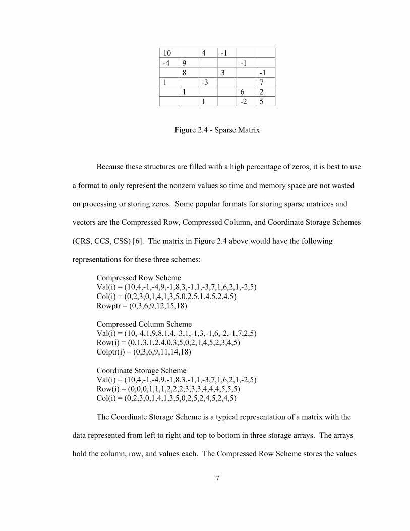
10 4 -1 -4 9 -1 8 3 -1 1 -3 7 1 6 2 1 -2 5
Figure 2.4 - Sparse Matrix
Because these structures are filled with a high percentage of zeros, it is best to use
a format to only represent the nonzero values so time and memory space are not wasted
on processing or storing zeros. Some popular formats for storing sparse matrices and
vectors are the Compressed Row, Compressed Column, and Coordinate Storage Schemes
(CRS, CCS, CSS) [6]. The matrix in Figure 2.4 above would have the following
representations for these three schemes:
Compressed Row Scheme Val(i) = (10,4,-1,-4,9,-1,8,3,-1,1,-3,7,1,6,2,1,-2,5) Col(i) = (0,2,3,0,1,4,1,3,5,0,2,5,1,4,5,2,4,5) Rowptr = (0,3,6,9,12,15,18)
Compressed Column Scheme Val(i) = (10,-4,1,9,8,1,4,-3,1,-1,3,-1,6,-2,-1,7,2,5) Row(i) = (0,1,3,1,2,4,0,3,5,0,2,1,4,5,2,3,4,5) Colptr(i) = (0,3,6,9,11,14,18)
Coordinate Storage Scheme Val(i) = (10,4,-1,-4,9,-1,8,3,-1,1,-3,7,1,6,2,1,-2,5) Row(i) = (0,0,0,1,1,1,2,2,2,3,3,3,4,4,4,5,5,5) Col(i) = (0,2,3,0,1,4,1,3,5,0,2,5,2,4,5,2,4,5)
The Coordinate Storage Scheme is a typical representation of a matrix with the
data represented from left to right and top to bottom in three storage arrays. The arrays
hold the column, row, and values each. The Compressed Row Scheme stores the values
7
and column addresses in two separate arrays in the same order as the Coordinate Storage
Scheme, except the row pointer, or “Rowptr”, array stores the index of the first number in
each row of the value array. As can be observed, less storage room is necessary when
using the row pointer array versus a full row array as in the Coordinate Storage Scheme.
This can become very important as the number of data become large. The Compressed
Column Scheme works like the Compressed Row Scheme except that values are stored
with respect to column order, the row values are stored in an array, and it has a column
pointer array instead of row pointer array.
The most popular storage format typically used with sparse matrix sparse vector
multiplication is the Compressed Row Scheme as it lends itself well to coding and
memory access for improved performance with respect to this problem. An advantage of
using these schemes is that pointer indexing can be used for the arrays, which is faster for
indexing large arrays than actual array indexing if programming in C. Because of this
advantage, linked lists are usually not used with large arrays.
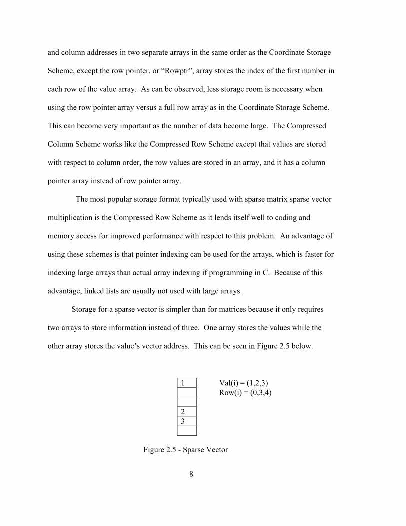
Storage for a sparse vector is simpler than for matrices because it only requires
two arrays to store information instead of three. One array stores the values while the
other array stores the value’s vector address. This can be seen in Figure 2.5 below.
1 Val(i) = (1,2,3) Row(i) = (0,3,4) 2 3
Figure 2.5 - Sparse Vector
8
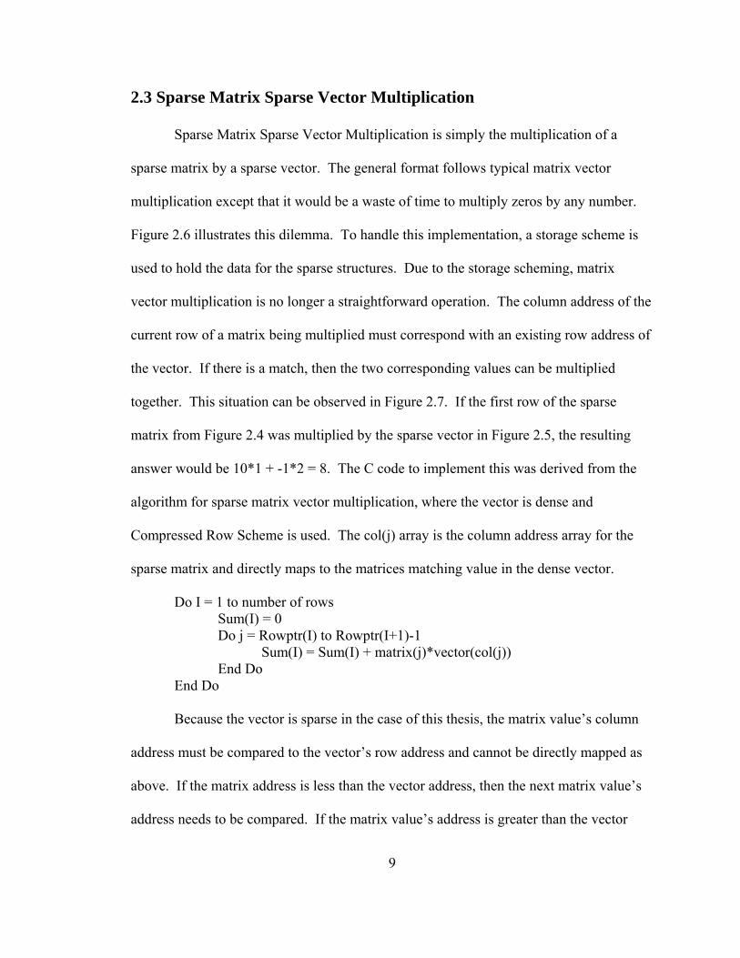
2.3 Sparse Matrix Sparse Vector Multiplication
Sparse Matrix Sparse Vector Multiplication is simply the multiplication of a
sparse matrix by a sparse vector. The general format follows typical matrix vector
multiplication except that it would be a waste of time to multiply zeros by any number.
Figure 2.6 illustrates this dilemma. To handle this implementation, a storage scheme is
used to hold the data for the sparse structures. Due to the storage scheming, matrix
vector multiplication is no longer a straightforward operation. The column address of the
current row of a matrix being multiplied must correspond with an existing row address of
the vector. If there is a match, then the two corresponding values can be multiplied
together. This situation can be observed in Figure 2.7. If the first row of the sparse
matrix from Figure 2.4 was multiplied by the sparse vector in Figure 2.5, the resulting
answer would be 10*1 + -1*2 = 8. The C code to implement this was derived from the
algorithm for sparse matrix vector multiplication, where the vector is dense and
Compressed Row Scheme is used. The col(j) array is the column address array for the
sparse matrix and directly maps to the matrices matching value in the dense vector.
Do I = 1 to number of rows Sum(I) = 0 Do j = Rowptr(I) to Rowptr(I+1)-1 Sum(I) = Sum(I) + matrix(j)*vector(col(j)) End Do End Do
Because the vector is sparse in the case of this thesis, the matrix value’s column
address must be compared to the vector’s row address and cannot be directly mapped as
above. If the matrix address is less than the vector address, then the next matrix value’s
address needs to be compared. If the matrix value’s address is greater than the vector
9
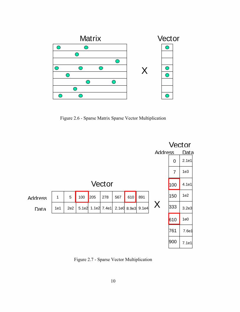
Figure 2.6 - Sparse Matrix Sparse Vector Multiplication
Figure 2.7 - Sparse Vector Multiplication
Matrix Vector
X
900 7.1e1
100
Vector
Vector
XAddress
Data
Address Data
1 5 100 205 278 567 610 891
1e1 2e2 5.1e2 1.1e2 7.4e1 .1e0 8.9e3 9.1e4
0
7
150
333
610
761
2.1e1
1e3
4.1e1
1e2
3.2e3
1e0
7.6e1
2
10
address’, then the next vector value’s address must be retrieved. If they both match, then
they are obviously multiplied together. This algorithm can be seen in the Appendix B
and is the C code that will be compared against the FPGA assisted processor.
The large amount of comparing necessary to implement the sparse matrix sparse
vector multiplication is where the sequential nature of software programming becomes a
weakness. Unfortunately for this algorithm, no optimization exists for an implementation
used for both structured and irregular sparse matrices. Specific algorithms can be created
for the optimization of structured sparse matrices but such an approach is beyond the
scope of this thesis. The critical question however is how often do address matches
typically occur; however, this cannot be answered unless the sparse matrix and vector
formats are known in advance, which affects the load balance of the problem.
2.4 Field Programmable Gate Arrays
Field Programmable Gate Arrays or FPGAs are prefabricated rows of transistor
and logic level gates attached to electronically programmable switches on a chip. To
program an FPGA, many different tools exist to accomplish such a task. Typically a
Hardware Description Language (HDL) is used to describe the behavioral and register
transfer level (RTL) of the FPGA. VHDL or Verilog are the two most popular used
hardware description languages. Programming an FPGA involves the development of
“processes”. A process is essentially a set of digital logic that continuously runs.
Creating multiple processes on one FPGA in essence creates a parallel architecture on a
chip that handles information on a bit or signal level. The ability to create multiple
processes all running simultaneously sharing and computing information on a bit level
gives FPGAs the capability to handle the processing of specific problems efficiently. The
11
more gates or transistors that are on one FPGA, the more data an FPGA can process at
one time. Because FPGAs are electronically reprogrammable, designs can quickly be
loaded, erased, and upgraded provided that designs have already been developed. Due to
the portable nature of HDLs, HDL designs can be used on many different FPGAs.
The use of FPGAs when improving existing problems is usually targeted to
exploit any and all redundancy and maximize parallelism through multiple processes.
This allows the use of FPGAs to out perform software programs where processing large
amounts of redundant information or parallelism can be exploited. Depending on the
complexity of the design, interfacing and synchronizing multiple processes can be
difficult. If used correctly, FPGAs could demonstrate beneficial performance
improvements.
2.5 Pilchard System
The Pilchard System [4] is an FPGA based platform that was developed by the
Chinese University of Hong Kong to add FPGA functionality to an existing computer.
While other systems that add FPGA functionality to computers utilize the PCI bus of a
computer to interface with an FPGA, the Pilchard System uses the memory bus.
Essentially an FPGA has been placed on a board which fits into a DIMM memory slot on
a computer and can be accessed using special read and write functions in C as if writing
and reading to and from the computer’s main memory. The advantage the Pilchard
System provides is the use of the faster memory bus over the slower PCI bus, which
allows for higher communication speeds in data processing.
The Pilchard System has a relatively light interface that helps HDL programmers
spend less time learning the system and allows for more room on the FPGA to be
12
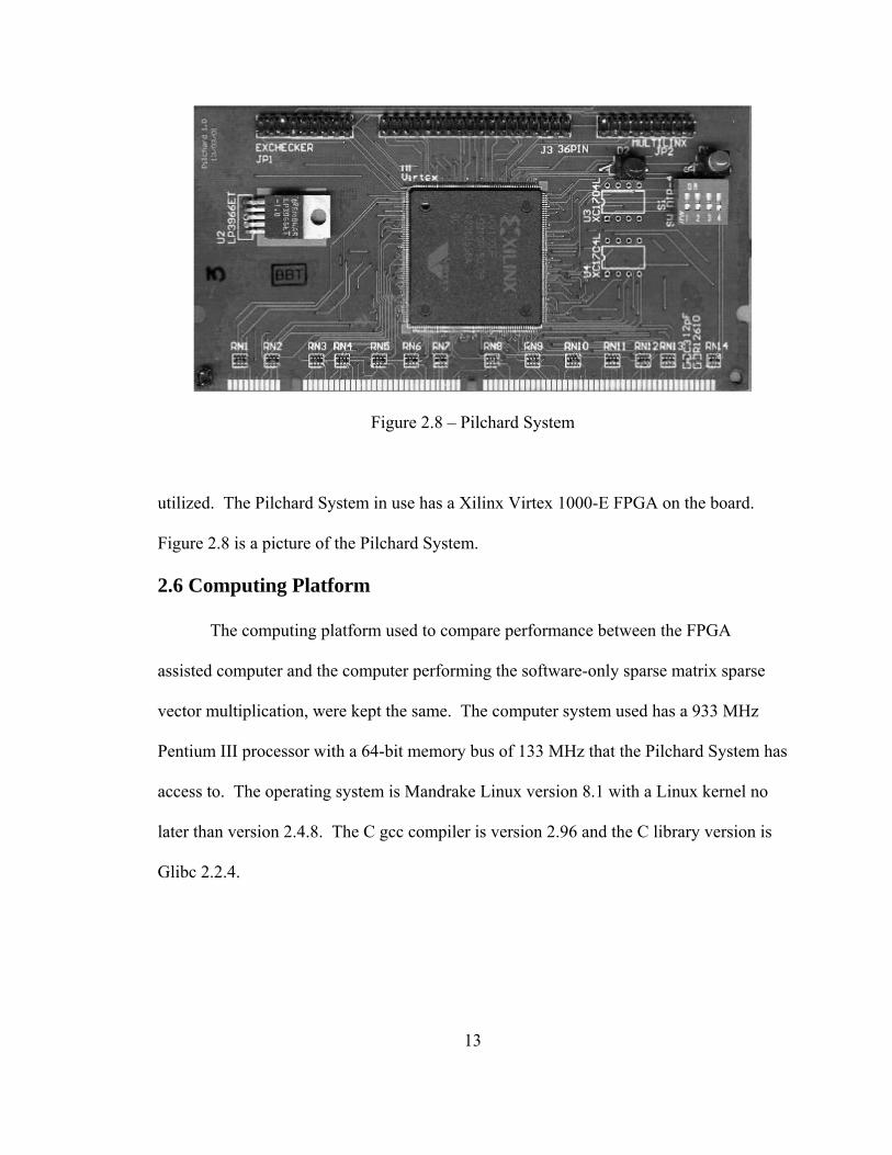
Figure 2.8 – Pilchard System
utilized. The Pilchard System in use has a Xilinx Virtex 1000-E FPGA on the board.
Figure 2.8 is a picture of the Pilchard System.
2.6 Computing Platform
The computing platform used to compare performance between the FPGA
assisted computer and the computer performing the software-only sparse matrix sparse
vector multiplication, were kept the same. The computer system used has a 933 MHz
Pentium III processor with a 64-bit memory bus of 133 MHz that the Pilchard System has
access to. The operating system is Mandrake Linux version 8.1 with a Linux kernel no
later than version 2.4.8. The C gcc compiler is version 2.96 and the C library version is
Glibc 2.2.4.
13
Chapter 3
Analysis of Related Work
3.1 Floating Point Multiplication and Addition on FPGAs
In the early stages of FPGA development and usage exploration, it was deemed
that FPGAs were not suitable for floating-point operations. This was mainly due to the
low density of early FPGAs being unable to meet the high demands of resources by
floating-point operations [8]. Floating-point operations involve separate processes to
handle the exponents, sign values, and fractions. These operations must normalize
portions of the floating-point data as well.
Shirazi, Walters, and Athanas [8], demonstrated that FPGAs became a viable
medium for floating-point operations in 1995 as Moore’s Law had time to alter the FPGA
landscape. Designs were created that supported eighteen and sixteen floating-point
adders/subtractors, multipliers, and dividers. Shirazi, et al., reported tested speeds of 10
MHz in their improved methods for handling addition/subtraction and multiplication all
using three stage pipelines. The multiplier had to be placed on two Xilinx 4010 FPGAs.
Seven years later in 2002, Lienhard, Kugel, and Männer [9] demonstrated the
ability of current FPGA technology of that time and its profound effect on floating-point
operations conducted on FPGAs. Essentially Moore’s Law had continued to provide
greater chip density as faster silicon was being produced. These authors reported design
frequencies ranging from 70 to 90 MHz for signed addition and 60 to 75 MHz for
multiplication.
14
In comparing the improvements in floating-point calculations over the last several
years, it as become apparent that floating-point operations can be done efficiently and
effectively thus lending them for co-processor uses.
3.2 Sparse Matrix Vector Multiplication on FPGAs
Sparse matrix vector multiplication is the multiplication of a sparse matrix and a
dense vector. Minimal work has actually been documented in applying this to FPGAs.
The need always exists for faster methods of handling sparse matrix vector
multiplication; however, the lack of information involving FPGA implementations leads
to minimal information regarding possible future implementations.
ElGindy and Shue [10] implemented a sparse matrix vector multiplier on an
FPGA based platform. In their research they used the PCI-Pamette, which is a PCI
board, developed by Compaq that houses five FPGAs with two SRAMs connected to two
of the FPGAs. The implementations explored used one to three multipliers and the
problem is described as a bin-packing problem. The bin-packing side of the problem is
handled by preprocessing on the host computer and the constant, or vector values are
stored before computation times are observed. When comparing results obtained, the
single multiplier is outperformed by the other two methods and by software. All of the
execution times grew quadratically as the size of the matrix grew, giving the performance
an O(n)2 appearance. The dual multiplier saw results close to that of the software
multiplier and the triple multiplier showed some improvements in performance over the
software multiplier. Performance was measured in clock ticks with the triple multiplier
taking roughly 200 clocks, the software and dual multipliers were around 50% slower and
the single multiplier was almost 4 times as slow as the triple multiplier. How these
15
multipliers are developed is not discussed in any detail. The performances of the FPGA
based implementations are only given for the core multiplication. No information is
provided as to how the preprocessing times affect results and if preprocessing is also
done for the software version.
3.3 Sparse Matrix Vector Multiplication on a Unary Processor
Sparse matrix vector multiplication on a single processor is widely used in
scientific computing, and circuit simulations among various other fields. Even though
the use of sparse matrix vector multiplication varies widely across industries, the basic
form remains unchanged. Wong [6] provides a simple model to compute sparse matrix
vector multiplication in compressed row storage and compressed column storage formats.
The very same format can be seen in multiple resources found through Netlib.org [11], a
major website that provides vast amounts of efficient computing algorithms in various
programming languages. The formula driving this algorithm was previously mentioned
in section 2.3 in compressed row storage. This algorithm simply uses a column address
(assuming compressed row storage) from the sparse matrix to pull the appropriate vector
data out for multiplication and accumulation, and can be performed in O(n) time where n
represents the number of nonzero elements in the sparse matrix. No more efficient
implementation of this algorithm has been found for sequential designs.
3.4 Sparse Matrix Vector Multiplication on Parallel Processors
Implementing sparse matrix vector multiplication on parallel processors has been
done with success. In general, the problem is distributed by rows of the sparse matrix
across the parallel processors. Wellein et al [12] demonstrated that use of parallel
16
machines could provide performance improvements that improve linearly with the
number of processors added to the overall design. Performance was measured in
gigaflops. Some of the machines that were used were vector computers and current
supercomputers such as SGI Origin3800, NEC SX5e, and Cray T3E to name a few.
Gropp, et al., [13] provide ways of analyzing realistic performance that can be
achieved on processors and parallel processors by simply evaluating the memory bus
bandwidth available. They simply state that the sparse matrix vector multiplication
algorithm is a mismatch for today’s typical computer architecture as can be seen by the
low percentage of performance observed to peak performance available by processors.
Geus and Röllin [14]evaluated the problem to improve eigenvalue solution
performance. Eigenvalue problems can compute sparse matrix vector multiplication
“several thousand times” for large sparse matrices and thus take up “80 to 95% of the
computation time.” Performance speedup was achieved by “pipelining the software” by
forcing the compiler to prefetch data. Matrix reordering and register blocking found
some additional improvements as well. The additions help improve performance in an
assisted sense. The same preprocessing techniques can be implemented in applying
designs to an FPGA. What makes Geus and Röllins’ research applicable is their
application of their parallel implementation on more standard parallel computing
platforms. The workload was again distributed by rows, more specifically in this case,
blocks of rows per processor. Performance improvements were seen from 48% (DEC
Alpha) to 151% (IBM SP2). These results also demonstrated that the inherent problem
scales well.
17
3.5 Sparse Matrix and Sparse Matrix Sparse Vector Multiplication
Virtually no resources are available in this area for reference, let alone discovery;
however, the need exists for scientific computations. These computations are used in
Iterative Solver [15] methods, Eigenvalue problems [6], and Conjugate Gradient methods
[6]. Khoury [15] also stated the lack of existing information regarding this area. Khoury
needed sparse matrix multiplication in solving blocked bidiagonal linear systems through
cyclic reduction. Khoury had to develop a sparse matrix multiplication method due to
being unable to find resources supporting such areas. Unfortunately, Khoury’s results
were skewed due to compilers unoptimizing the design and the heap not being cleaned
appropriately.
Sparse matrix multiplication is an area of interest; however, due to the very core
of its operation being sparse vector multiplication. Sparse vector multiplication is also
the basis behind sparse matrix sparse vector multiplication. Sparse matrix sparse vector
multiplication can then be looked as a core component of sparse matrix multiplication. In
speeding up sparse matrix sparse vector multiplication, sparse matrix multiplication can
be sped up as a result.
18
Chapter 4
Design Approach
The flow of the design process involves making assumptions and providing an in-
depth analysis of the problem. In observing the big picture considering sparse matrix
sparse vector multiplication running in software on a stand-alone processor, the biggest
possible limitation was considered to involve the sequential compares. Due to this
observation, the FPGA design was built around the parallelization of the compares and
the supporting components. The following sections will discuss the assumptions made,
analysis of the problem, analysis of the hardware limitations, detailed partitioning of the
problem, and design of the implementation on a FPGA.
4.1 Assumptions
To help constrain the problem to reasonable limitations to allow for an effective
implementation of sparse matrix sparse vector multiplication, some necessary
assumptions are required. All assumptions made apply to both the HDL and to the C
algorithm used except where an assumption can only apply to the HDL.
4.1.1 Limited IEEE 754 Format Support
In the design of the floating-point multiplier and accumulator, support is not given
to all features of the standard. The floating-point multiplier and adder can at the least
handle, NaN, zero, and infinite valued results but that is all. Neither of the two support
rounding, invalid operations, or exceptions including the handling of underflow and
overflow. Overflow should not be an issue since rounding is not supported. Invalid
operations are those such that there is a divide by zero, magnitude subtraction by
19
infinites, and an operation involving a NaN among other scenarios. A full list can be
found in the IEEE 754 Standard.
4.1.2 Use of Compressed Row Scheme
The assumption is made that all sparse matrices used are formatted using the
Compressed Row Scheme. This is so there are no discrepancies in performance of data
that use different storage format schemes. This constraint also helps simplify the design
process by limiting the support to one input format. The storage scheme will be
combined with only using the C programming language to eliminate performance
discrepancies across various programming languages.
4.1.3 Sparse Matrix and Sparse Vectors
It is assumed that the design involved in this scope of work is to improve
performance of sparse matrix sparse vector multiplication. All matrix and vector
structures that are not sparse will not have competitive performance results as that is out
of the design scope; however, the ability for dense matrices and vectors to be solved will
be available. This is necessary as a portion of a sparse matrix and sparse vector
multiplication could have the potential of appearing dense. Since this possibility is
supported, dense matrix vector multiplication can be accomplished but with a significant
cost in performance. Dense matrices and vectors are still expected to conform to the
Compressed Row Scheme.
4.1.4 Generic Design Approach
In the consideration and design of this sparse matrix sparse vector multiplication
algorithm, a general approach towards the possible sparse matrix structure is assumed.
Due to the vast types of structured sparse matrices, many designs would be necessary to
20
cover them all. This design is to have the capability to solve any type of sparse matrix.
This also makes the assumption that no optimizations are made towards any particular
sparse matrix structure such that it might reduce the performance of a different structured
sparse matrix.
4.1.5 No Pre-Processing
It is also assumed that no pre-processing of matrices or vectors will take place. It
is recognized that pre-processing of sparse matrices and even sparse vectors can help
improve performance; however, the implementation would then be constrained to one
particular type of sparse matrix sparse vector multiplication. That would defeat the
purpose of not optimizing for any one particular type of sparse matrix structure.
4.1.6 Addressable Range
The addressable range for data will be limited by 32-bits in any one particular
dimension. This means the potential address span of a matrix could be 4,294,967,296 by
4,294,967,296. The vector address range must also be able to support up to a 32-bit
address value.
4.2 Analysis of the Problem
In analyzing the overall problem to solve the multiplication of sparse matrices
with sparse vectors, one key critical area appears to allow for the most improvement
given the sequential nature of the C programming language. This important area is the
penalty paid by the C program if the address values for a matrix and vector value do not
match. When this occurs, the program must then begin searching through the next
address values of the matrix or vector, comparing the addresses one-by-one until a match
is found or no match can exist. This searching adds another nested for loop to the
21
algorithm thus creating a potential O(n3) worst case scenario to solve the matrix vector
multiplication. It is this main point that the FPGA design will focus upon.
As mentioned earlier, the sequential nature of the C code prevents the algorithm
from handling concurrency in the processing of a piece of data multiple times at once.
The more parallelism that can be explored and put to use in the FPGA design, the greater
the benefit can become for using an FPGA.
4.3 Analysis of Hardware Limitations
The hardware limitations imposed by the equipment being used is important to
mention, because it ultimately has a significant impact on the overall design. Limitations
can be found on the FPGA, Pilchard System, Memory Bus, and Computer system used
with the underlying theme of memory limitations.
The FPGA used, the Xilinx Virtex 1000-E, has its own limitations being
resources. This FPGA part has approximately 1.5 million gates, 12,288 slices and 4Kbits
of block RAM. While this may appear like plenty, the double precision multiply
accumulator uses 26% of the available slices, 18% of the FF Slices, 21% of the LUTs,
and 120,000 gates. If using Dual Port RAM [16] IP from Xilinx to hold data leaving and
entering the Pilchard System as is customarily done, that will cost over 70,000 gates.
Very quickly 20-25% of the FPGA’s resources have been used as an absolute minimum
for the sparse matrix sparse vector multiplication design to work with. While the design
will likely fit, room for improvements like adding an additional adder or even multiply
accumulator will become difficult if not impossible. Another issue regarding limitations
of the current FPGA is its age. The Xilinx part being used is becoming obsolete, as there
are much larger and faster FPGA parts available today. While how a design is created in
22
23
Memory Bus
SMSV
Pcore Pilchard
HDL has the largest effect on overall system speed, that overall system speed is limited
by the speed of the logic available on the FPGA itself. If a faster and larger chip were to
be available the design would have better performance as more parallel compares could
also fit. The effects the FPGA size and speed has on the overall design will be explored
further in the Results, and Conclusions and Future Work Chapters.
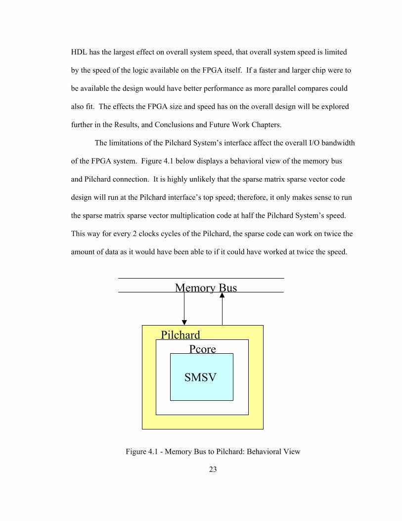
The limitations of the Pilchard System’s interface affect the overall I/O bandwidth
of the FPGA system. Figure 4.1 below displays a behavioral view of the memory bus
and Pilchard connection. It is highly unlikely that the sparse matrix sparse vector code
design will run at the Pilchard interface’s top speed; therefore, it only makes sense to run
the sparse matrix sparse vector multiplication code at half the Pilchard System’s speed.
This way for every 2 clocks cycles of the Pilchard, the sparse code can work on twice the
amount of data as it would have been able to if it could have worked at twice the speed.
Figure 4.1 - Memory Bus to Pilchard: Behavioral View
This then puts more pressure on the Pilchard System’s interface to operate at a higher
speed since the code beneath it will be running at half that. Unfortunately, simply
passing information through the Pilchard at its top speed of 133MHz is too difficult for it
to handle. This makes the target top speed for the code underneath it (likely limited by
the floating-point unit speeds) slower than hoped. Due to the Pilchard operating at twice
the clock speed as the sparse operating code, the Pilchard then needs to read in 2 64-bit
values from the memory bus in two clock cycles so that it may send 128-bits for every
sparse code clock cycle. Although the code to handle this is relatively straightforward
and not very complicated, producing results that operate allow the Pilchard to operate at
100Mhz will remain a challenge.
An additional limitation of the Pilchard System is the lack of onboard RAM or
cache. This requires that the Pilchard then take the time to access main memory, which is
costly, while the C code has the benefit of being able to take advantage of cache. If the
Pilchard Board were to have onboard RAM and/or cache, the entire vector and extremely
large portions of the matrix could quite possibly be stored right on the board itself, saving
the Pilchard System and sparse matrix sparse vector code time in having to constantly use
and compete for the memory bus for data.
Another major limitation is the memory bus itself. The memory bus operates at
133 MHz and is 64-bits wide; therefore only 1 double precision floating-point value can
be passed per bus clock cycle. This will put a significant strain on the memory bus as
potentially thousands to hundred of thousands of double precision values will be passed
along the memory bus alone, not to mention all of the 32-bit address values that need to
be compared. Two 32-bit address values can be passed per clock cycle.
24
4.4 Partitioning of the Problem
With the necessary assumptions made, analysis of the problem completed, and
hardware limitations explored, the problem can then be partitioned. When partitioning a
problem four main factors need to be considered to achieve the best possible load
balance. These factors are decomposition, assignment, orchestration, and mapping [17].
Decomposition involves exposing enough concurrency to exploit parallelism, but not too
much such that the cost of communication begins to outweigh the benefits of parallelism.
Assignment considers the assignment of data to reduce communication between
processors and balance workload, and efficiently interfacing parallel processes is what
orchestration entails. This means reducing communication through data locality,
reducing synchronization costs, and effective task scheduling. Mapping is simply
exploiting existing topology and fitting as many processes on the same processor as
effectively possible.
Altering one of these attributes of a parallel design effects the other attributes.
Ideally some sort of complete balance is achieved between them all. These attributes will
be addressed specifically or implied as the problem is partitioned in the subsequent
sections. The greater the understanding of both the software and hardware issues, the
more effective the partitioning process can be, which leads to a more complete design.
The decomposition and mapping stages are essentially predetermined due to hardware
limitations and data format already being determined. The data has already been
decomposed into 64-bit double precision floating-point values and 32-bit address values.
The only other area of decomposition is in the parallel comparators, which is attempting
to create the maximum number of parallel compares on the FPGA. As for mapping, the
25
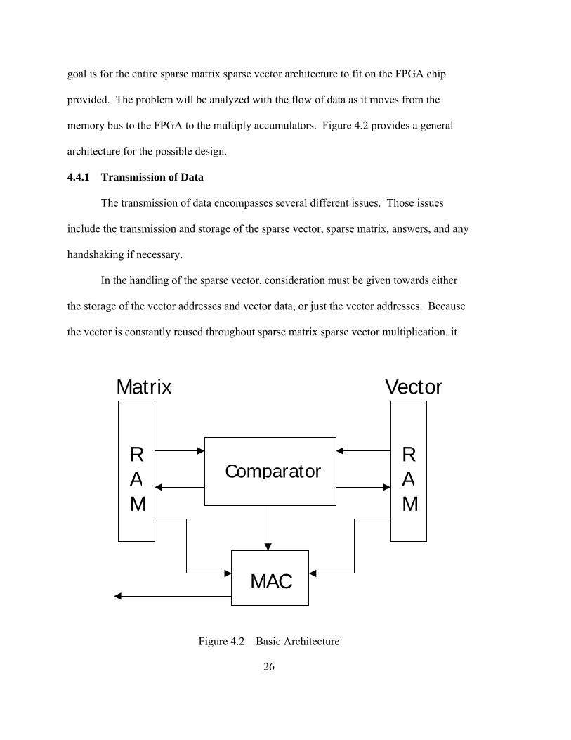
goal is for the entire sparse matrix sparse vector architecture to fit on the FPGA chip
provided. The problem will be analyzed with the flow of data as it moves from the
memory bus to the FPGA to the multiply accumulators. Figure 4.2 provides a general
architecture for the possible design.
4.4.1 Transmission of Data
The transmission of data encompasses several different issues. Those issues
include the transmission and storage of the sparse vector, sparse matrix, answers, and any
handshaking if necessary.
In the handling of the sparse vector, consideration must be given towards either
the storage of the vector addresses and vector data, or just the vector addresses. Because
the vector is constantly reused throughout sparse matrix sparse vector multiplication, it
Comparator
MAC
RAM
RAM
VectorMatrix
Figure 4.2 – Basic Architecture
26

only makes sense to store the vector information and not resend the same information
repeatedly. In determining how much of the sparse vector to store, as much as
reasonably possible should be stored due to the large amount of reuse in the comparison
of matrix column addresses and vector addresses. If only the vector addresses are stored,
it would result in a reduced overhead for storing the vector data; however, it would cost
more to send the vector value when a match is repeatedly found for one vector location.
Consideration could also be given to storing vector values only after a match is found
instead of storing them when they may or may not be needed. The cost for sending the
vector data when needed would ideally be the same as sending the value before knowing
if it is needed. This way unnecessary resources are not spent in transmitting vector
values that will never be needed. The downside to following this path is that the
complexity to handle this format would be increased on both the FPGA side and
supporting C code. Additional logic would be needed to determine if the vector value
exists and how to handle the request of it. The space would have to be available to store
all possible vector values for each address stored so there would be no benefit in memory
reduction, only in overall performance so long as the extra complexity does not negate
the benefits. Both vector address and value could be stored, with the convenience of
having all necessary vector data available at the cost of memory usage. Registers are
inexpensive on an FPGA and thus a large number of vector data could be stored to make
the additional overhead cost worthwhile.
After determining the storage scheme for the sparse vector, it is more than likely
that the entire vector will not fit all at once on the FPGA. This makes the decision of
27
how to store the sparse vector even more important because the more often a new section
of the vector is stored, the more often the vector loading overhead will be incurred.
When sending matrix information over the memory bus to the FPGA, similar
issues are encountered as with the vector transmission, which was determining whether to
send matrix values with the addresses, or just the addresses alone. If matrix addresses
were accompanied by their values, then those values would be readily available to begin
multiplication. If the values were not needed, they would simply be discarded. The
downside to sending the values with addresses is that if the values are not needed then
time was wasted on the bus sending the information. The less matches there are per
compare, the more costly. If considering sending the addresses alone, after a match is
found the matrix value could be requested by the FPGA. While this format may reduce
the waste of matrix value transmissions, some form of handshaking would have to be
introduced to notify the C code what values need to be sent. Unless performed cleverly,
handshaking could be costly and it disrupts any notion of streaming data to the FPGA.
The final area to evaluate in data transmission is how data is transmitted over the
memory bus itself. This partly depends on the storage scheme of vectors and how matrix
information is processed. In regards to sending vector information to the FPGA, if both
vector values and addresses are transmitted then simply transmitting two addresses in one
clock and the corresponding values the next two clock cycles should be efficient. The
memory bus would be utilized to the fullest. If vector values were transmitted as needed
then they would need to be transmitted after a certain number of compares have been
processed. The C code would need to know what vector value(s) to transmit; therefore,
the FPGA would have to initiate some form of handshaking. Upon completion of
28

handshaking, the C code should send only the necessary vector values in the order needed
by the FPGA.
In the former method mentioned of sending vector values with addresses, the data
can simply be streamed in until all vector registers are full. In the latter format, vector
addresses could be streamed in, but values would only be transmitted after some
additional handshaking to notify the C code of what is needed. In general, vector
transmission is a cost only paid when necessary to load up vector data or send vector
values separately.
Most of the bus time will be spent sending matrix information instead of vector
information in the overall scheme of things. Here, two main different methods are
explored, streaming and block transfer. The streaming method is tied to the transmission
of both matrix addresses and values. This could be accomplished by sending two address
values in one memory bus clock cycle followed by two clock cycles of sending the two
corresponding values. The C code and FPGA code should already have a set number of
transmissions before either needing to take any special action.
The block transfer method would send a set number of matrix addresses or block
of addresses, and the FPGA would respond in some manner with a request for matrix
values if there were a match. The C code would then send the correct matrix values for
multiplication. This block transfer process would be repeated as necessary.
In comparing the two different data transmission methods, both have their
advantages and disadvantages. The streaming method requires no loss of time in having
to implement any handshaking. A disadvantage of streaming; however, is that two out of
every three clock cycles are spent sending data that may or may not be needed when most
29
of the time addresses are needed for comparing. The block transfer method does not
waste valuable clock time in transmitting unwanted matrix values, but additional
handshaking is necessary which has its own penalties to be paid. All of these different
methods have their advantages and drawbacks.
4.4.2 Logic Flow
The flow of logic and data must be controlled in some fashion as it enters the
FPGA because there is not enough bandwidth to handle requests for comparison
information, multiply information, handshaking, and answers all simultaneously. The
entire design has one 64-bit bus to utilize therefore the data trafficking must be
controlled. Several different possible states must be considered. Data needs to go to
comparators in some efficient and highly parallel manner, data needs to fill vector
information stored on the FPGA, and data needs to be directed to the multiply
accumulators. Also, the state machine will need to accommodate the ability to send
information back to memory bus for the C code to retrieve. In addition to the state
machine providing all of the necessary states, it must flow between states in a logical
manner and have the capability to jump to any necessary state given any possible
condition. The state machine should also be able to protect the sparse matrix sparse
vector code from operating when it should not. Ideally the state machine will help
improve orchestration between processes. Also, in orchestrating the processes and data
communication, a balanced workload should be strived for by keeping the assignment of
data dispersed appropriately.
30
4.4.3 Comparing of Addresses
As the flow of data moves from the memory bus to the state machine, it should be
sent into a structure to handle parallel comparisons. This is essentially the main reason
for this entire implementation of a sparse matrix sparse vector multiplication. Ideally the
more parallel compares that can be implemented the better; however, a few
considerations need to be made. As the number of simultaneous compares increase, the
more room on the FPGA is used. At the very least, enough space needs to be provided
for a floating-point multiply accumulator as well as minimal control for data flow. To
accommodate greater amounts of concurrent comparators, the capability needs to exist to
handle the possible large amount of data resulting from all of the comparing. One giant
comparator cannot efficiently do all of the comparing at once as it would be too slow, so
the comparing would have to be divided in multiple processes. The more processes
running, the more individual results there are to multiplex. If more than one element of
the matrix is being compared then a matching result can exist for as many elements of the
matrix being compared. This creates a dynamic load balance of results being passed on
to the multiply accumulator. When and how often multiple results will be calculated is
unknown and can make handling the results difficult. Dynamic task scheduling must
then be employed to help balance possible imbalanced results passed on to the multiply
accumulators. The increased complexity becomes very real as parallel comparators are
added and increased in size while trying to achieve optimal performance. In determining
how to handle this portion of the design, a balance needs to be achieved between creating
as many compares as possible, with still being able to provide the means to handle the
results under desired operating speeds.
31
4.4.4 Multiply Accumulator
Performing any kind of matrix vector multiplication requires the use of multiply
accumulation. When a row of a matrix is multiplied to the matching elements of a vector,
all of the multiplication results need to be accumulated for the resulting answer vector’s
corresponding element. When performing this operation on sparse matrix sparse vector
data, the essential nature remains the same of needing to multiply values together and
sum those results. Constructing such an architecture to handle this is not as obvious as
handling dense matrices and vectors where maximum parallelization can be achieved due
to the static scheduling nature of information and results. In consideration of sparse
matrix sparse vector multiplication on an FPGA sharing resources, loading balancing
becomes a factor as well as limited real estate for placing MACs.
The effects of an imbalanced load and the uncertainties of the frequency at which
address matching will occur, complicates multiply accumulator design immensely. These
unknowns make it extremely difficult if not impossible to create an optimized
architecture when designing for the general case with capabilities to handle any situation.
The multiply accumulator design must therefore be able to handle dense matrices and
vectors. Obviously performance will suffer heavily for dense data since that is not the
target of the design, but what level of sparseness to target the design, cannot be
determined so it must be prepared to handle all sparseness. The structure of the sparse
matrix and sparse vector also play a part. What is important given the limited design
space is that the “best bang for the buck” is achieved. In other words, in the
determination of how many multipliers and accumulators are to be used; it is desired that
all of the arithmetic units placed on the FPGA stay busy. There is no point in wasting
32
space on the chip if arithmetic units are not used often, because it is all about designing
for the average or general case and getting the most out of what is available or in use.
Another issue to observe when creating the multiply accumulation units is how to
handle answers or the sums created. Ideally, one or multiple answers could be found at
one time. The problem in doing so range from discerning one sum from the next, to
knowing which values in the pipelined adder correspond to what partial sum. Unless
there are multiple multiply accumulator units available to keep track of their own sum,
keeping track of multiple sums would become difficult and complex even though the
capability would be convenient. Traversing an entire row of the matrix and vector to
obtain just one sum would create the need to reload the entire vector per matrix row. This
would become costly due to not maximizing reuse; therefore, the multiply accumulator
must solve for a partial sum for a given row of the answer vector. In simplifying the
work of handling vector storage and reuse, handling partial sums instead of full sums
becomes another complexity to consider. It must then be determined if the FPGA or the
computer keeps track of the partial sums, while keeping in mind that there could be a few
partial sums to thousand upon thousands of them. If handling partial sums, each partial
sum can be sent back out to the CPU to let it finish each sum. As can be seen as the data
flows from the memory bus down to the multiply accumulators into answers, the effects
of each part all tie in to each other and will be put together in one design in the following
section.
4.5 FPGA Design
The architecture of the sparse matrix sparse vector multiplication algorithm
attempts to utilize the partitioning of the problem to the highest degree possible. The
33
overall design has been broken down into six major components, the interface to the
Pilchard System or Pcore, State Machine, Comparators, Multiply Accumulator Interface,
the Double Precision Floating-Point Multiplier and Adder, and the C code that is used to
interface to the Pilchard System from the user side.
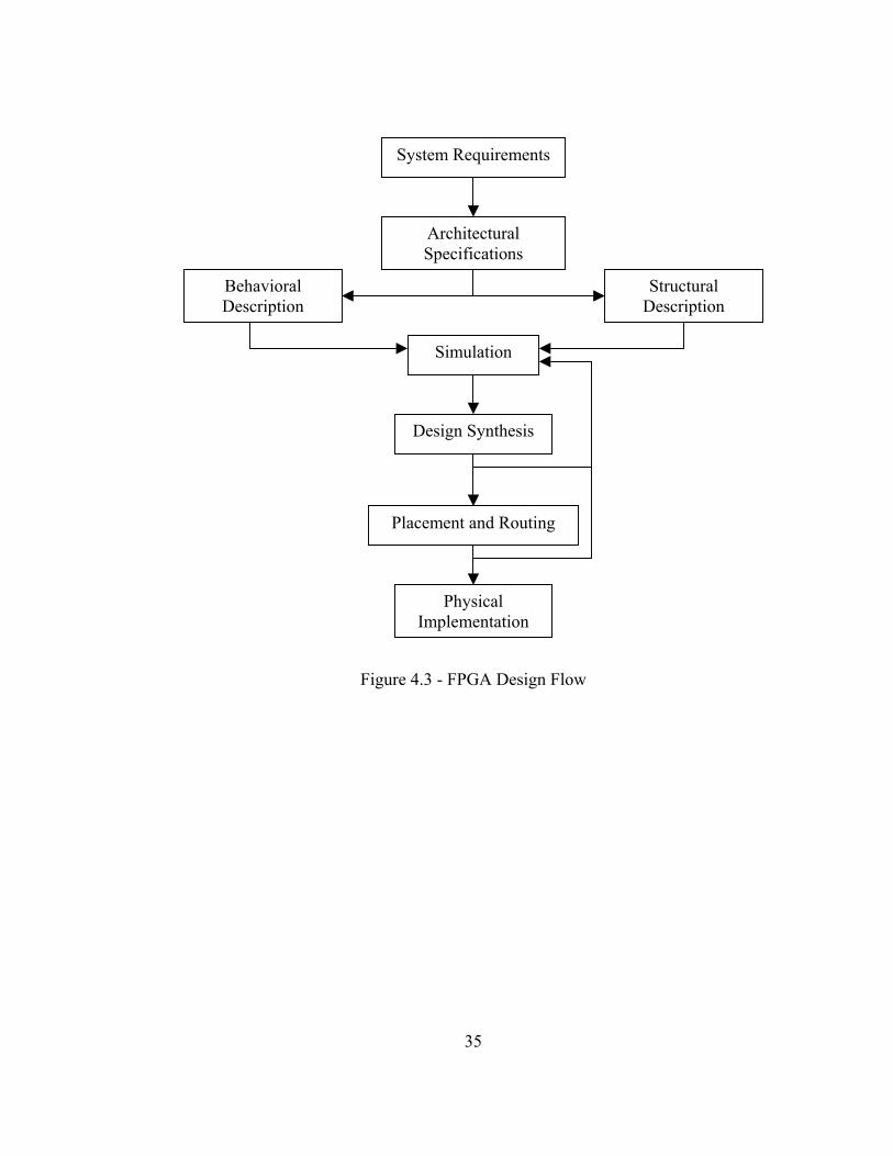
In developing these components in HDL, the flow chart in the Figure 4.3 shows
the general design flow process in developing HDL for a FPGA. Essentially, after the
specifications and requirements of a system have been determined, HDL in the form of
behavioral and structural code formats is simulated to check for accuracy. If simulation
provides accurate results, the design is then synthesized and re-simulated, or post-
synthesis simulation. After post-synthesis simulation produces valid results, the design is
place and routed which provides the real design that will go into an FPGA. The place
and routed design is also simulated to check for accuracy. If the design continues to
prove accurate, it is placed on the FPGA for actual implementation. Unfortunately, the
Pilchard System does not currently allow support for simulation after synthesis or place
and route. This deficiency is critical as these simulations can often show design flaws
that pre-synthesis simulation cannot, thus making debugging of actual performance
extremely difficult.
In general, the sparse matrix sparse vector multiplier reads in 128-bits of
information in one clock cycle. With this information, vector addresses and values are
both stored on the FPGA to minimize the complexities of having to request vector values
on an as needed basis. After storing a vector, matrix addresses are compared to vector
addresses in mass parallel. Sending in 56 addresses in one block transfer, 4 separate
matrix addresses per sparse code clock, achieves this block transfer size. The
34
System Requirements
Architectural Specifications
Behavioral Description
Structural Description
Simulation
Design Synthesis
Placement and Routing
Physical Implementation
Figure 4.3 - FPGA Design Flow
35
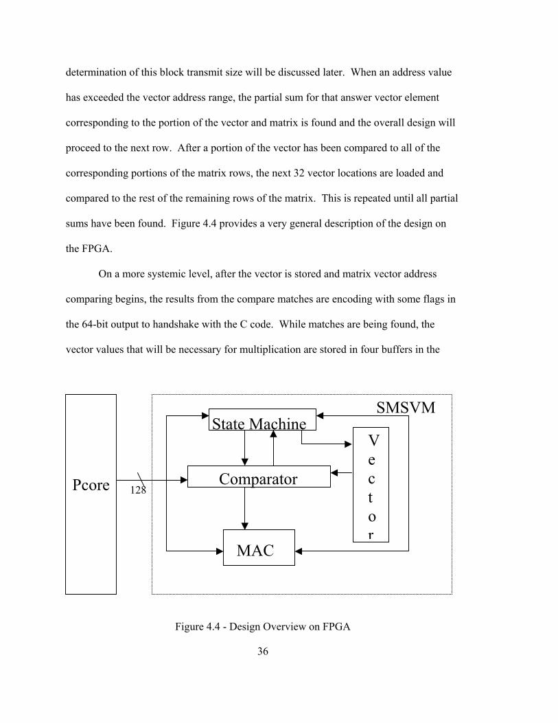
determination of this block transmit size will be discussed later. When an address value
has exceeded the vector address range, the partial sum for that answer vector element
corresponding to the portion of the vector and matrix is found and the overall design will
proceed to the next row. After a portion of the vector has been compared to all of the
corresponding portions of the matrix rows, the next 32 vector locations are loaded and
compared to the rest of the remaining rows of the matrix. This is repeated until all partial
sums have been found. Figure 4.4 provides a very general description of the design on
the FPGA.
On a more systemic level, after the vector is stored and matrix vector address
comparing begins, the results from the compare matches are encoding with some flags in
the 64-bit output to handshake with the C code. While matches are being found, the
vector values that will be necessary for multiplication are stored in four buffers in the
SMSVM State Machine
Comparator
MAC
Vector
128 Pcore
Figure 4.4 - Design Overview on FPGA
36
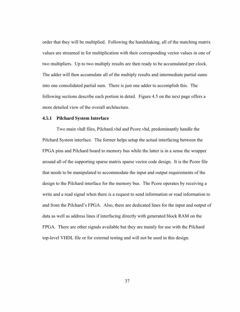
order that they will be multiplied. Following the handshaking, all of the matching matrix
values are streamed in for multiplication with their corresponding vector values in one of
two multipliers. Up to two multiply results are then ready to be accumulated per clock.
The adder will then accumulate all of the multiply results and intermediate partial sums
into one consolidated partial sum. There is just one adder to accomplish this. The
following sections describe each portion in detail. Figure 4.5 on the next page offers a
more detailed view of the overall architecture.
4.5.1 Pilchard System Interface
Two main vhdl files, Pilchard.vhd and Pcore.vhd, predominantly handle the
Pilchard System interface. The former helps setup the actual interfacing between the
FPGA pins and Pilchard board to memory bus while the latter is in a sense the wrapper
around all of the supporting sparse matrix sparse vector code design. It is the Pcore file
that needs to be manipulated to accommodate the input and output requirements of the
design to the Pilchard interface for the memory bus. The Pcore operates by receiving a
write and a read signal when there is a request to send information or read information to
and from the Pilchard’s FPGA. Also, there are dedicated lines for the input and output of
data as well as address lines if interfacing directly with generated block RAM on the
FPGA. There are other signals available but they are mainly for use with the Pilchard
top-level VHDL file or for external testing and will not be used in this design.
37
State Machine
CMPA
CMPB
CMPC
CMPD
V E C T O R
Dynamic Task Allocation
F I F O 1
FI FO2
FI FO3
FI FO4
MULT 1 MULT 2
ADDER
MAC Controller
MAC FIFO
Flags
6464
64
64128
32
32
32
32
P C O R E
Figure 4.5 - Detailed Architectural View of Sparse Matrix Sparse Vector Multiplier
38
SMSVM
AsyncFIFO
Controller
PCORE P I L C H A R D
R A M
CLK CLKDIV
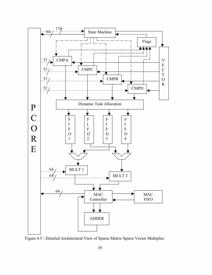
Figure 4.6 - Pcore
When developing the Pcore, the requirements and needs of the underlying system
are important. The necessary components can be seen in Figure 4.6 above. Since the
sparse matrix sparse vector multiplication will be operating on a clock cycle twice as long
as Pcore’s clock, it is important that the synchronization between clocks and the
communication of information between those clocks is accurate. To make-up for the
slower speed of the matrix vector multiplication, twice the amount of memory bus data
can be sent to the sparse code to operate on. Pcore will have the capability to read in two
64-bit values in two clock cycles and pass one 128-bit value on to the sparse code in one
sparse code clock cycle. This allows the memory bus to stream data in, while providing a
way to get the information to the sparse matrix sparse vector code on a slower clock.
The difficulty lies in the synchronization of passing the data back and forth
between the top level Pilchard structure and the slower clock of the sparse code. The
39
slower clock is based off of a clock divider from the main clock and will be referred to as
clockdiv. Because the faster clock operates at twice the speed of clockdiv, the 128-bits
being passed along to the sparse code needs to be held long enough for the sparse code to
accurately retrieve the 128-bits. To accomplish this, an asynchronous FIFO buffer was
generated using Xilinx’s Coregen program. This generated core can handle reading data
on one clock while writing data out on a different clock. Due to the core being available
for professional use, it is reliable and can handle the asynchronous data transfer
effectively. The use of this asynchronous FIFO was a convenient and time saving
solution to handle the memory bus to sparse matrix sparse vector code data transfer.
When passing answers back from the sparse code through the Pcore out of the
FPGA, Xilinx’s Coregen block RAM was used. Using block RAM to output data
ensured that data would be stabilized for the memory bus to read from. This is important
due to interfacing two different clock speeds again. The depth of the RAM was four.
Currently only two locations are in use; however, that can be expanded if desired.
4.5.2 State Machine
The state machine is the main interface to the Pcore when controlling the data
read into the FPGA and also for controlling and monitoring the sparse matrix sparse
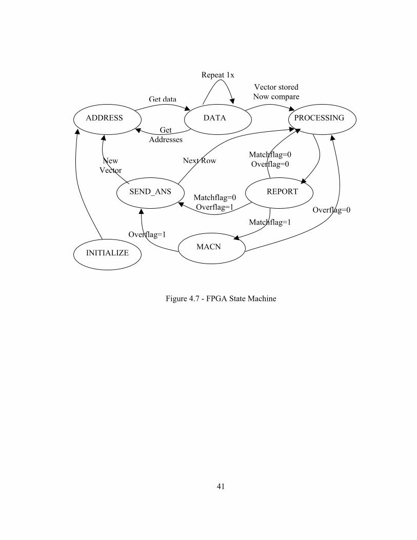
vector multiplication process. The different states utilized to accomplish this are:
INITIALIZE, ADDRESS, DATA, PROCESSING, REPORTw, REPORTx, SEND, and
MACN. All states check an input signal called “din_rdy” that when goes high, notifies
everything that valid 128-bits of input are available. If this signal is not high, the state
machine simply holds its current status and position. Figure 4.7 gives a graphical
representation of the state machine.
40
ADDRESS DATA PROCESSING
SEND_ANS REPORT
MACN
New Vector
Next Row
Get data
Get Addresses
Overflag=1 Matchflag=1
Matchflag=0 Overflag=1 Overflag=0
Vector stored Now compare
Repeat 1x
Matchflag=0 Overflag=0
INITIALIZE
Figure 4.7 - FPGA State Machine
41
The INITIALIZE state is run first and only once. It receives the first writes from
the C code, which notify the state machine of how many rows exist in the matrix. This is
necessary so that the state machine knows when it is handling the last row so it can
transition to appropriate states. After this state, the state machine moves to the
ADDRESS state.
The ADDRESS state receives the address data for the vector and stores the
addresses in registers. Registers are used for storage to help simplify their frequent
access by the compators. Due to the 128-bit input, 4 32-bit addresses can be
simultaneously stored into registers in one clock cycle. After the four addresses are read
from the input, the state machine will transition to the DATA state for the next two clock
cycles.
The DATA state breaks the 128-bit input into 2 64-bit inputs, which represents
vector data, in one clock cycle and stores them into block RAM designated to hold vector
values. Because in the previous state; 4 addresses were read in, the DATA state is held
for 2 clock cycles so that it will have read in 4 vector values. After reading in 4 vector
values, the state machine transitions back to the ADDRESS state. The transition back
and forth between these two states goes on until 32 vector addresses and values have all
be input into the vector registers. When this is done, the state machine moves on to the
PROCESSING state.
The PROCESSING state constantly reads in matrix addresses for mass parallel
comparing. This state keeps count of how many input values have been read in using a
decrementing counter. The counter allows for 14 block transfers of 4 matrix addresses
42
each. When the counter is zero, the maximum number of address values has been read in
and the state will transition to the REPORTw and REPORTx states.
The two REPORT states are executed successively. The REPORTw stage is the
next stage after PROCESSING, and it buffers the 1 clock delay required to ensure all
comparing is done so the comparator results can be sent to the C code. This one clock
delay is necessary for the transition from REPORTw to REPORTx state. The REPORTw
state is left out of the diagram for simplification. In the REPORTx state, information is
gathered from all of the comparing of addresses. All of this information is used to notify
the C code if there were any address matches, what addresses had matches, if the matrix
addresses went over the current address range stored on the vector, and a special last
address match flag. All of this information must fit into one 64-bit output signal to
simplify the number of clocks of handshaking down to one. Five bits ended up being
extra and are reserved for future use. One bit each is reserved for the match flag, over
flag, and last address match flag. The overflag signals to the C code that a matrix address
wnt past the vector address range. The match flag indicates that there was at least one
match, and the last address match flag indicates if the last bit in the 56-bit encoded
compare result stands for a match if equal to one. This is done for redundancy checking
to ensure the very last bit is transmitted correctly. The remaining 56 bits are used to
encode which matrix addresses matching occurred on. This will be described in the
Comparator section. After reporting the status of compares back to the C code,
depending on the status, the state machine will transition to one of three states: the
MACN, SEND, or back to PROCESSING state. The MACN state has first priority, as it
needs to be next if there were any address matches. The SEND state has second priority
43

meaning if there were no matches and the over flag is high, then a partial sum needs to be
found based on the current data that has been input and calculated to be sent to the C
code. Last priority is given to moving to the PROCESSING state. This is only done if
there were no matches and the over flag has not been set high; therefore, continue
processing more matrix addresses.
If the MACN state is next, all of the matrix values that correspond to matches will
be read in, in order. As these values are read in, they are sent to two multipliers to be
multiplied with their corresponding vector values. Because there is no dedicated signal to
the FPGA to notify it when the C code is done sending matrix values, the C code will
send in all zeros when it is done. This is necessary because the “din_rdy” flag is already
in use to notify the MACN stage if it even needs to be looking for valid input. It is
possible that there may be a delay in sending matrix values to the FPGA; therefore, an
input of all zeros will be acceptable. If the MACN stage receives all zeros as an input, it
knows it is time to move on to the next state. The purpose for sending all zeros as
notification is due to the fact that a zero should never be stored as a matrix value to begin
with because zero values should not be stored, thus providing flexibility in reading
inputs. After reading in all of the input values, the state machine will transfer to the
SEND stage if the over flag is high; otherwise if no answer needs to be sent, go back to
the PROCESSING state.
In the SEND state, the state machine simply waits for the floating-point multiply
accumulator to find the current partial sum. When the partial sum is ready, the state
machine notifies Pcore that an answer is ready to be sent out from the FPGA. When this
is done, the state machine checks if the flag was set to notify it that the last row of the
44
matrix was being processed. If so, then the state machine needs to go back to the
ADDRESS state to begin loading a new vector; otherwise, the state machine will transfer
back to the PROCESSING state to begin handling another partial sum for a different
matrix row.
4.5.3 Comparators
Each comparator is made up of four parallel compare processes for each of the
four matrix addresses input per clock during the PROCESSING state. Each process
handles 8 compares in one clock cycle for a total of 128 simultaneous compares in one
clock cycle. This is where the strength of the design lies. Figure 4.8 displays the overall
comparator design in its entirety with an individual compare process shown in greater
detail.
For each of the four processes per matrix address, only one match can exist, as all
vector addresses are unique per row. After the initial 32 compares per matrix address are
executed, the four individual process results are multiplexed to check for a match. If
there is a match, several different tasks occur. One task is that the corresponding vector
value for that match is grabbed and sent off to a dynamic task scheduler to handle the
random nature that multiple matches may occur. What the dynamic task scheduler does
is keep all of the matches in order in the four buffers that will feed the two floating-point
multipliers. Each buffer is filled in order as a match is found, so if buffer one is filled
first, buffer two is next. After buffer two, buffer three is next and so on. After buffer
four is filled, the dynamic task scheduler should assign the next matched vector value to
the first buffer. Due to the random matching nature, the next buffer to fill on a clock
45

CMPA
CMPB
CMPC
CMPD
Dynamic Task
Scheduler
Input (127->96)
Input (95->64)
Input (63->32)
Input (31->0)
128bits
0
78
1516
2324
31
Vector Addresses
8 CMPs
8 CMPs
8 CMPs
8 CMPs
MUX
Dynamic Task
Scheduler
Matrix Addr
Input (127->96)
CMPD
Figure 4.8 - Comparator System
46
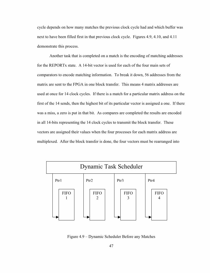
cycle depends on how many matches the previous clock cycle had and which buffer was
next to have been filled first in that previous clock cycle. Figures 4.9, 4.10, and 4.11
demonstrate this process.
Another task that is completed on a match is the encoding of matching addresses
for the REPORTx state. A 14-bit vector is used for each of the four main sets of
comparators to encode matching information. To break it down, 56 addresses from the
matrix are sent to the FPGA in one block transfer. This means 4 matrix addresses are
used at once for 14 clock cycles. If there is a match for a particular matrix address on the
first of the 14 sends, then the highest bit of its particular vector is assigned a one. If there
was a miss, a zero is put in that bit. As compares are completed the results are encoded
in all 14-bits representing the 14 clock cycles to transmit the block transfer. These
vectors are assigned their values when the four processes for each matrix address are
multiplexed. After the block transfer is done, the four vectors must be rearranged into
FIFO 1
FIFO 2
FIFO 3
FIFO 4
Dynamic Task Scheduler
Ptr1 Ptr2 Ptr3 Ptr4
Figure 4.9 – Dynamic Scheduler Before any Matches
47
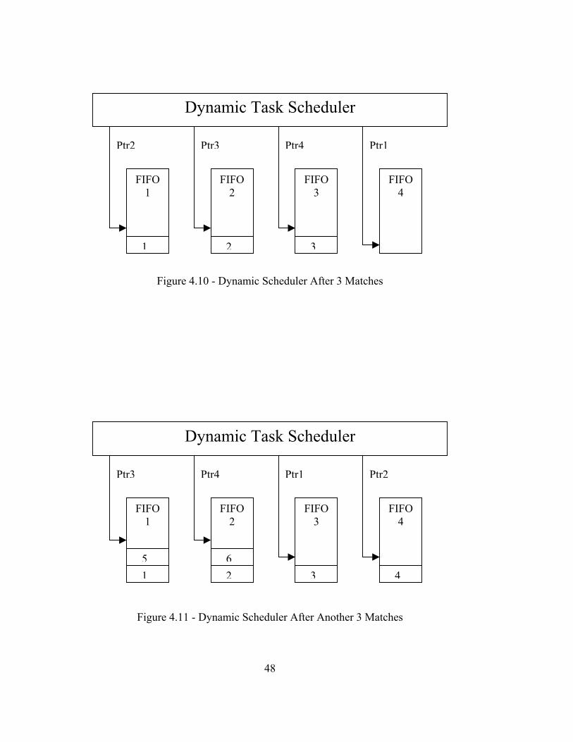
FIFO 1
FIFO 2
FIFO 3
FIFO 4
Dynamic Task Scheduler
Ptr2 Ptr3 Ptr4 Ptr1
1 32
Figure 4.10 - Dynamic Scheduler After 3 Matches
FIFO 1
FIFO 2
FIFO 3
FIFO 4
Dynamic Task Scheduler
Ptr3 Ptr4 Ptr1 Ptr2
1 32 45 6
Figure 4.11 - Dynamic Scheduler After Another 3 Matches
48
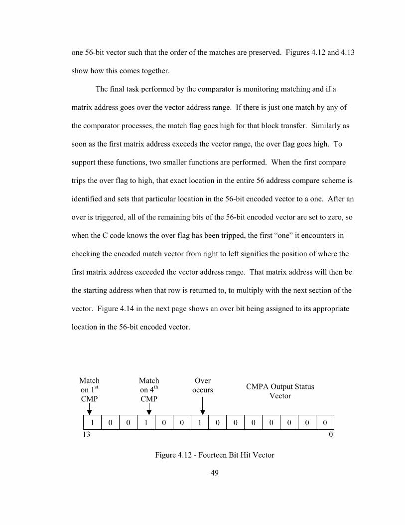
one 56-bit vector such that the order of the matches are preserved. Figures 4.12 and 4.13
show how this comes together.
The final task performed by the comparator is monitoring matching and if a
matrix address goes over the vector address range. If there is just one match by any of
the comparator processes, the match flag goes high for that block transfer. Similarly as
soon as the first matrix address exceeds the vector range, the over flag goes high. To
support these functions, two smaller functions are performed. When the first compare
trips the over flag to high, that exact location in the entire 56 address compare scheme is
identified and sets that particular location in the 56-bit encoded vector to a one. After an
over is triggered, all of the remaining bits of the 56-bit encoded vector are set to zero, so
when the C code knows the over flag has been tripped, the first “one” it encounters in
checking the encoded match vector from right to left signifies the position of where the
first matrix address exceeded the vector address range. That matrix address will then be
the starting address when that row is returned to, to multiply with the next section of the
vector. Figure 4.14 in the next page shows an over bit being assigned to its appropriate
location in the 56-bit encoded vector.
1 0 0 0 0
Match on 1st CMP
Match on 4th CMP
Over occurs CMPA Output Status
Vector
1
30
Figure
0
14.12 - Four
4
0
1teen Bit Hi
9
0
t Vector
0
0 0 0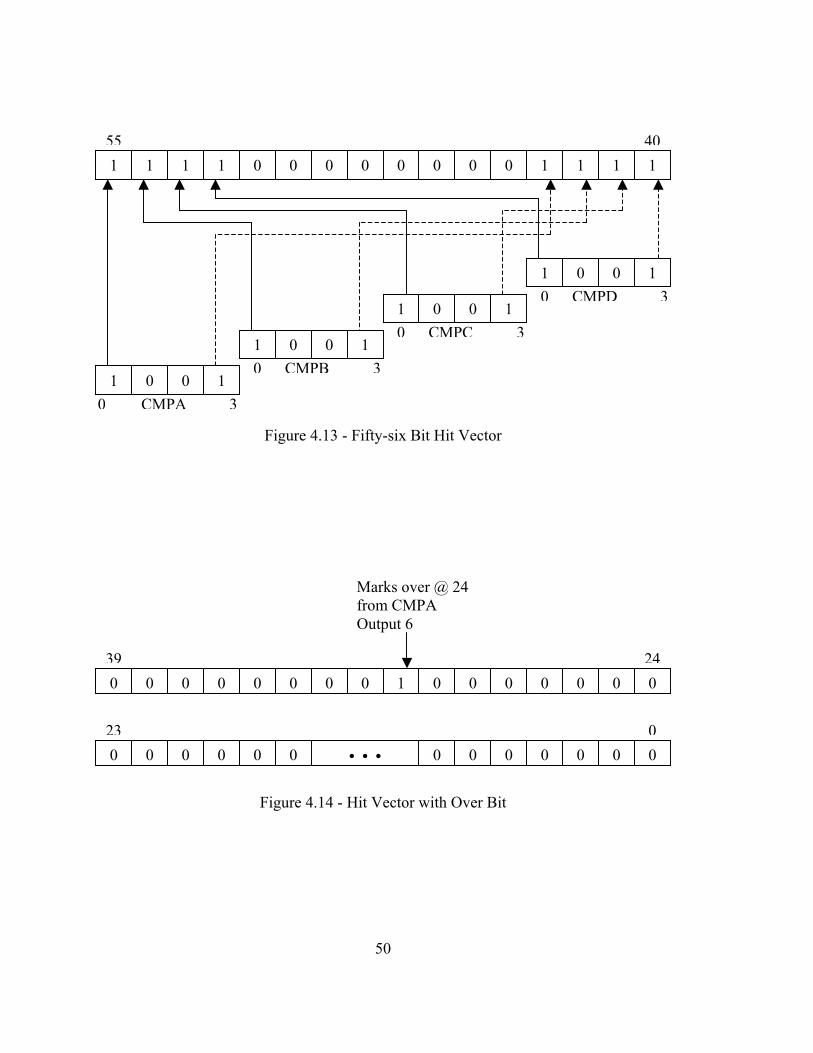
1 0 0 1
1
1
1
1
Fig
0
0
Fig
0
0ure 4.13 -
ure 4.14 - H
0
1
Fifty-six Bi
0
Marks ovefrom CMPOutput 6
it Vector w
50
0
0t Hit Vecto
r @ 24 A
ith Over B
0
1
r
0
0
it
1
11
1
1
0 01
0 01
0 01
0 0CMPA
CMPD
CMPC
CMPB
0
0
0
0
55
400
00
3
3
3
3
0
0 0 0 0 0 0 1 0 0 0 0 39 240
0 0 0 0 0 0 0 0 0 23. . .
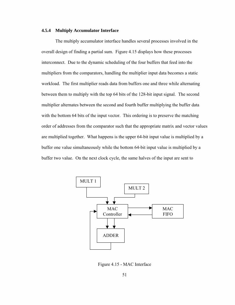
4.5.4 Multiply Accumulator Interface
The multiply accumulator interface handles several processes involved in the
overall design of finding a partial sum. Figure 4.15 displays how these processes
interconnect. Due to the dynamic scheduling of the four buffers that feed into the
multipliers from the comparators, handling the multiplier input data becomes a static
workload. The first multiplier reads data from buffers one and three while alternating
between them to multiply with the top 64 bits of the 128-bit input signal. The second
multiplier alternates between the second and fourth buffer multiplying the buffer data
with the bottom 64 bits of the input vector. This ordering is to preserve the matching
order of addresses from the comparator such that the appropriate matrix and vector values
are multiplied together. What happens is the upper 64-bit input value is multiplied by a
buffer one value simultaneously while the bottom 64-bit input value is multiplied by a
buffer two value. On the next clock cycle, the same halves of the input are sent to
MULT 1MULT 2
ADDER
MAC Controller
MAC FIFO
Figure 4.15 - MAC Interface
51
the same multipliers, but multipliers one and two get their vector values from buffers
three and four respectively. This alternating sequence continues until all data has been
sent in for multiplication. The advantage in using two multipliers and four buffers lies in
that there is no backup of data on the FPGA, the two 64-bit multipliers can handle the
128-bit input.
As the multiplication results are found, they are fed into an adder. Over time,
addition results are accumulated into one partial sum, but the process of accumulation is
complex. Due to the pipelined nature of the adder, results cannot be available on the next
clock following the input. As the number of values to accumulate drop below what can
fit in the pipeline, the values must be temporarily stored in a buffer until another result is
available to be added with. There will be times when there are so many values to
accumulate, that accumulation has not finished before the next round of multiplication
results come in. Soon monitoring all of the data to be summed becomes difficult. Input
to the adder can come from two multipliers, the output of the adder, and the FIFO buffer
used to store overflow. The combination of obtaining these values and when they are
available is complex. There could be two multiplication results available or there could
be only one. There could be an adder result available too. Not helping the situation is if
data is being stored in the buffer. When data is requested from the buffer, there is a two-
clock cycle delay. Depending on if data is requested from the buffer, as the second or
first input into the adder is another issue as well.
To begin sorting out this complication, priorities must be set as to what
component’s result has the highest and lowest priority with respect to being an input into
52
the adder. The multiplication results are given the highest priority because their four
buffers must be cleared as soon as possible to avoid a backup of matching vector value
information. If a backup were to occur, the system as a whole would have to stall, a
situation to be avoided if possible. Because they are given such priority and the MACN
stage can have the buffers cleared during that state, this potential back up is avoided.
Multiplier one will have priority over multiplier two as multiplier one would be handling
a greater number of matches if the number of matches is odd. Next in line on the priority
chain is the adder result. Last priority is given to retrieving data from the buffer. A mini-
pipeline is established to handle the funneling of data into the adder, mainly due to the
possibility of there being one answer available for a clock or two before another potential
input is ready. This pipeline is also used to time input into the adder upon a request for
data from the buffer. When one input is available and waiting for another input, the first
input will hang around for two clock cycles. If no other input is available at that time, it
is written to the buffer to wait for a longer period for another input. When multiple
inputs are present, the prioritized scheme is used to determine what values get put into the
adder and what value is written to the buffer.
Some complications involved in using a buffer with a delayed output is that if a
request has been made for buffer data, it then holds the “trump card” over all other inputs.
This is because of the complicated nature of timing its availability with the
unpredictability of other inputs. If the first input for the adder is a call to the buffer for
input, the process monitoring all the activity will wait for another input to be available
while the buffer output is taking its two clock cycles to come out. If something becomes
available, the newly available data is sent to one of three stages to time it with the
53
buffer’s output into the adder. If more than one piece of data becomes available while
waiting on output from the buffer, the priority scheme kicks in. If two inputs are
available, one will be sent into to the buffer while the other will be sent with the buffer
output to the adder. If data is available from both multipliers and the adder while not
waiting for output from the buffer, an overflow signal must be used to store the second
extra piece of data available. The worst-case scenario is, when two values are being
pulled from the buffer (one ahead of the other) and values become available from the
multipliers and the adder. Now both buffer outputs hold the highest priority, one
multiplication result gets written to the buffer, the other multiplication results is written to
the overflow signal, and the adder result is written to a second overflow signal.
Fortunately this worst-case scenario cannot happen in consecutive clocks or every other
clock as it takes that many clocks for such a situation to develop. This allows time
immediately following the worst-case scenario to clear out the two overflow signals so
they are not overwritten. Another reason why the worst-case scenario cannot repeat itself
is once multiplication results are incoming and the worst-case scenario has occurred, for
the next several clock cycles the multipliers will control the inputs into the adder thus
flushing out any remaining multiplication results so the worst-case scenario still cannot
repeat itself. All adder results in the meantime are written to the buffer.
4.5.5 Double Precision Floating-Point Multiplier and Adder
The floating-point multipliers and adder both handle double precision (64-bit)
data and are pipelined processes. The multipliers are 9 pipeline stages and the adder has
13 pipeline stages. Both support the IEEE 754 format and are constrained as mentioned
in the Assumptions section.
54
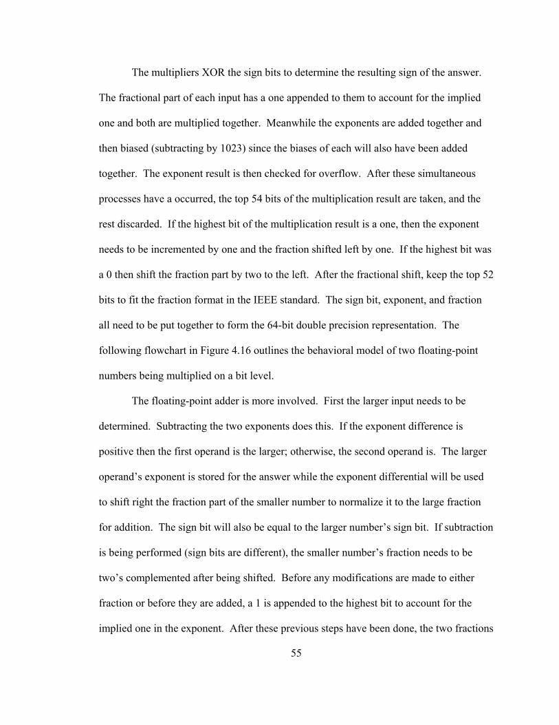
The multipliers XOR the sign bits to determine the resulting sign of the answer.
The fractional part of each input has a one appended to them to account for the implied
one and both are multiplied together. Meanwhile the exponents are added together and
then biased (subtracting by 1023) since the biases of each will also have been added
together. The exponent result is then checked for overflow. After these simultaneous
processes have a occurred, the top 54 bits of the multiplication result are taken, and the
rest discarded. If the highest bit of the multiplication result is a one, then the exponent
needs to be incremented by one and the fraction shifted left by one. If the highest bit was
a 0 then shift the fraction part by two to the left. After the fractional shift, keep the top 52
bits to fit the fraction format in the IEEE standard. The sign bit, exponent, and fraction
all need to be put together to form the 64-bit double precision representation. The
following flowchart in Figure 4.16 outlines the behavioral model of two floating-point
numbers being multiplied on a bit level.
The floating-point adder is more involved. First the larger input needs to be
determined. Subtracting the two exponents does this. If the exponent difference is
positive then the first operand is the larger; otherwise, the second operand is. The larger
operand’s exponent is stored for the answer while the exponent differential will be used
to shift right the fraction part of the smaller number to normalize it to the large fraction
for addition. The sign bit will also be equal to the larger number’s sign bit. If subtraction
is being performed (sign bits are different), the smaller number’s fraction needs to be
two’s complemented after being shifted. Before any modifications are made to either
fraction or before they are added, a 1 is appended to the highest bit to account for the
implied one in the exponent. After these previous steps have been done, the two fractions
55
Sign Exponent Fraction Value
E1
E F
Bias Adjust
XOR Add Append 1
Multiply
S1
S
F1 F2S2 E2
MSBMSB
Incr. by 1 Shift Left 1
Shift Left 2
=1 =0
=1
=0 ? ?
S E F
Figure 4.16 - Floating-Point Multiplier Flow Chart
56
are summed. After the fractions are added, the resulting fraction must be shifted left until
the highest bit was one to renormalize the fraction. The sign bit, exponent, and resulting
fraction are all appended together in order to form the double precision addition result.
The flowchart in Figure 4.17 depicts this process.
4.5.6 C code interface
The C code that will interface with the Pilchard System is an optimized code that
is written to cater to the state machine inside of the FPGA; therefore, to a large degree the
state machine of the C code will look identical to the FPGA state machine. The Pilchard
System comes with a special header file and C file that defines special functions to map
the Pilchard to memory, and to read and write to the Pilchard System. The Read64 and
Write64 commands will read and write 64 bits of data and the inputs to the functions are
assigned their values by using pointers. This is so 64-bit double precision values do not
have to be manipulated in order store the data in upper and lower 32-bit halves of the data
type required for the special read and write functions.
The C code will begin by opening up the necessary files that are in CRS format,
check to see how big the matrix and vector both are, dynamically allocate space, and
store all of the data in arrays. After closing those files, the Pilchard space in memory will
then be initialized. Now the processing can begin. The C code has several states,
INITIALIZE, SEND_VADDR, SEND_VDATA, CMPING, GET_STATUS,
SEND_MDATA, and GET_ANS. The code will start out in the INITIALIZE state by
sending the FPGA the number of rows in the matrix. It will then transition to the
SEND_VADDR state by sending two addresses consecutively to achieve the 4 32-bit
57
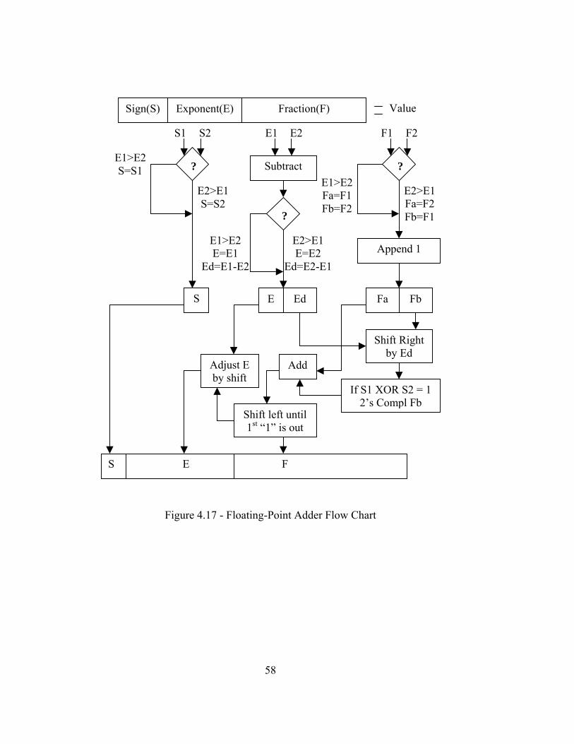
Sign(S) Exponent(E) Fraction(F) Value
S E F
E1 S1 F1 F2 S2 E2
? ? Subtract
?
E1>E2 S=S1
E2>E1 S=S2
E2>E1 Fa=F2
E1>E2 Fa=F1 Fb=F2
E2>E1 E=E2
Ed=E2-E1
E1>E2 E=E1
Ed=E1-E2Append 1
E Ed Fa Fb
Add
S
Fb=F1
Figure 4.17 - Floating-Point Adder Flow Cha
58
Shift Right by Ed
If S1 XOR S2 = 1 2’s Compl Fb
Shifst
t left until1 “1” is out
Adjust Eby shift
rt
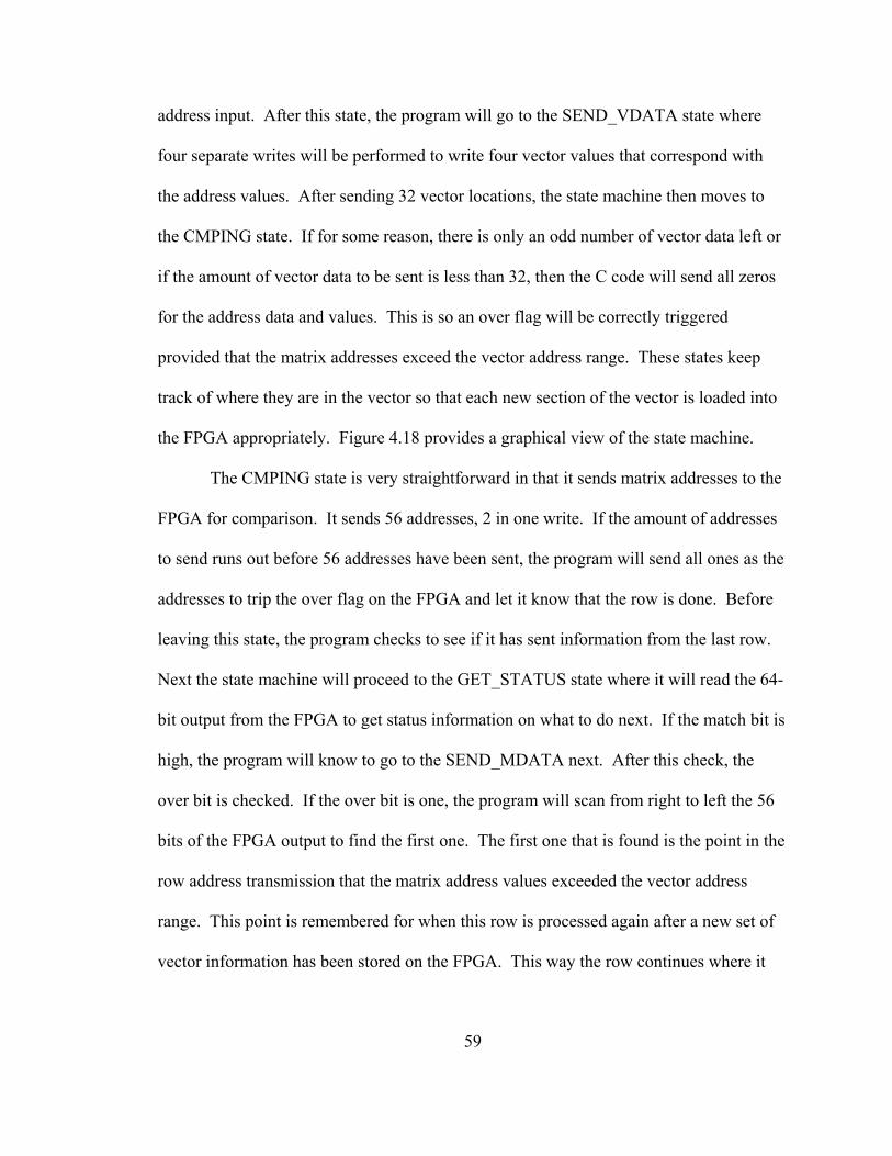
address input. After this state, the program will go to the SEND_VDATA state where
four separate writes will be performed to write four vector values that correspond with
the address values. After sending 32 vector locations, the state machine then moves to
the CMPING state. If for some reason, there is only an odd number of vector data left or
if the amount of vector data to be sent is less than 32, then the C code will send all zeros
for the address data and values. This is so an over flag will be correctly triggered
provided that the matrix addresses exceed the vector address range. These states keep
track of where they are in the vector so that each new section of the vector is loaded into
the FPGA appropriately. Figure 4.18 provides a graphical view of the state machine.
The CMPING state is very straightforward in that it sends matrix addresses to the
FPGA for comparison. It sends 56 addresses, 2 in one write. If the amount of addresses
to send runs out before 56 addresses have been sent, the program will send all ones as the
addresses to trip the over flag on the FPGA and let it know that the row is done. Before
leaving this state, the program checks to see if it has sent information from the last row.
Next the state machine will proceed to the GET_STATUS state where it will read the 64-
bit output from the FPGA to get status information on what to do next. If the match bit is
high, the program will know to go to the SEND_MDATA next. After this check, the
over bit is checked. If the over bit is one, the program will scan from right to left the 56
bits of the FPGA output to find the first one. The first one that is found is the point in the
row address transmission that the matrix address values exceeded the vector address
range. This point is remembered for when this row is processed again after a new set of
vector information has been stored on the FPGA. This way the row continues where it
59
SEND_VADDR SEND_VDATA CMPING
GET_ANS GET_STATUS
SEND_MDATA
New Vector
Next Row
Send data
Send Addresses
Overflag=1 Matchflag=1
Matchflag=0 Overflag=1 Overflag=0
Vector sent Now compare
Repeat 3x
Matchflag=0 Overflag=0
Repeat 1x
INITIALIZE
Figure 4.18 – C Code State Machine
60
left off. After finding the over bit, that bit is set to zero. This is done because the
SEND_MDATA stage will check these bits for a one, and will send the corresponding
data if a one is found. After all of the over processing is done, or after a match flag is
found without the over flag equal to one, the state machine will transfer to one of three
states: SEND_MDATA, GET_ANS, or CMPING. If the match flag was high, the state
machine will go to the SEND_MDATA state next. If the over flag was high then the
state machine transitions to the GET_ANS state; otherwise, the CMPING state is next.
If the state machine goes to the SEND_MDATA stage, the program will traverse
the 56-bit match vector from left to right to send matching data in order. After gathering
two matches it will write the two matrix values. If there are an odd number of matches,
the program will send in dummy data so that there have been an even number of writes
(so the asynchronous FIFO gets 128-bits in Pcore – the FPGA will not process dummy
data). After the matching data has been sent, all zeros are sent to notify the FPGA that all
data has been sent. This occurs when 56 values have been transmitted or while sending
data, if the stop-point is reached (point at where an “over” occurred), the state will
terminate the sending of data and send in all zeros to signify that it is done. If the over bit
is high the state machine then moves to the GET_ANS state, otherwise it moves on to the
CMPING state.
The GET_ANS state simply waits in this state for a valid answer to present itself
from the FPGA. When it does, the partial sum is taken and added to the existing partial
sum for that particular row in the answer vector. If the program had been processing the
last row of the matrix (but not the last row and set of columns) it will then go to the
61

SEND_VADDR state to send in new vector data and start processing the next chunk of
the matrix. If the last row and column were just processed then the program has finished;
otherwise, the program will proceed to the CMPING stage where the next set of row
addresses will be compared.
62
Chapter 5
Results
The following chapter summarizes the results of the FPGA assisted computer’s
design implementation in comparison to the stand-alone processor’s results. Several
points of interest will be observed and evaluated to help distinguish the differences and
similarities in the results. The overall performance of the FPGA design yielded slower
results than hoped in that the stand-alone processor outperformed the FPGA design. The
design was place and routed with timing constraints of 50 MHz for the sparse matrix
sparse vector portion of the FPGA while the Pcore interface ran at 100 MHz bus speed so
it could supply 128 bits per 50 MHz clock. Approximately 70% of the FPGA’s slices
were used and approximately 60 of the 96 block RAM locations were also utilized. The
following sections will discuss and interpret the results and difficulties encountered in
developing a double precision floating-point sparse matrix sparse vector multiplier on a
FPGA.
5.1 Comparison of Results
In the process of evaluating results, it is important to properly put them in
perspective. To accomplish this, various characteristics of sparse matrix sparse vector
multiplication data will be utilized in the analysis of the results, which are: overall
performance, hits (when a matrix element address and vector address match to yield a
FPMAC), compares, hits-to-compares ratio (Ψ), quantity of nonzero values, the number
of vector loads, and percentage of theoretical MFLOPS achieved. Several sets of test
data were used to determine all of the following evaluations. When observing these
63

results, dataset 4 was varied four times with those variations all yielding extremely
similar results. A table with all of the statistics regarding each dataset can be viewed in
Appendix A.
The performance of the FPGA assisted implementation proved to be slow at best
when compared to the stand-alone computer’s performance. Across the various tests, the
stand-alone’s performance averaged 50-60 times faster than the FPGA assisted
computer’s implementation. This slow-down will be discussed further in the difficulties
section later in this chapter. The figures throughout this chapter depict the difference in
computational performance to the characteristics mentioned above. In the all of the
graphs, the legend shows the curves for the “CPU time” and “FPGA time” where the
“CPU time” refers to the total time for the stand-alone processor to compute its results,
while the “FPGA time” represents the time taken for the FPGA and supporting CPU to
compute its results. Both times include the time spent communicating the data over the
memory bus. Due to the large performance difference between designs, all
characteristics plotted versus performance are done on both a base 10 and logarithmic
scales for execution time. Also, all graphs with time being represented by the y-axis, is
in microseconds.
Figure 5.1 plots performance time versus the datasets used. The performance
slow-down in the FPGA design is obvious when comparing results between the two
design implementations. This graph depicts the 50-60x performance difference
throughout the datasets. The performance of the two designs appear to mimic one
another on the logarithmic scaled graph in Figure 5.2.
64

Overall Performance
0
500
1000
1500
2000
2500
Data 1 Data 2 Data 3 Data 4a Data 4b Data 4c Data 4d Data 5
Data Set
Tim
e (u
s)
CPU timeFPGA time
Figure 5.1 - Dataset Performances
Overall Performance
1
10
100
1000
10000
Data 1 Data 2 Data 3 Data 4a Data 4b Data 4c Data 4d Data 5
Data Set
Tim
e (L
og u
s)
CPU timeFPGA time
Figure 5.2 - Dataset Performances (Log Scale)
65
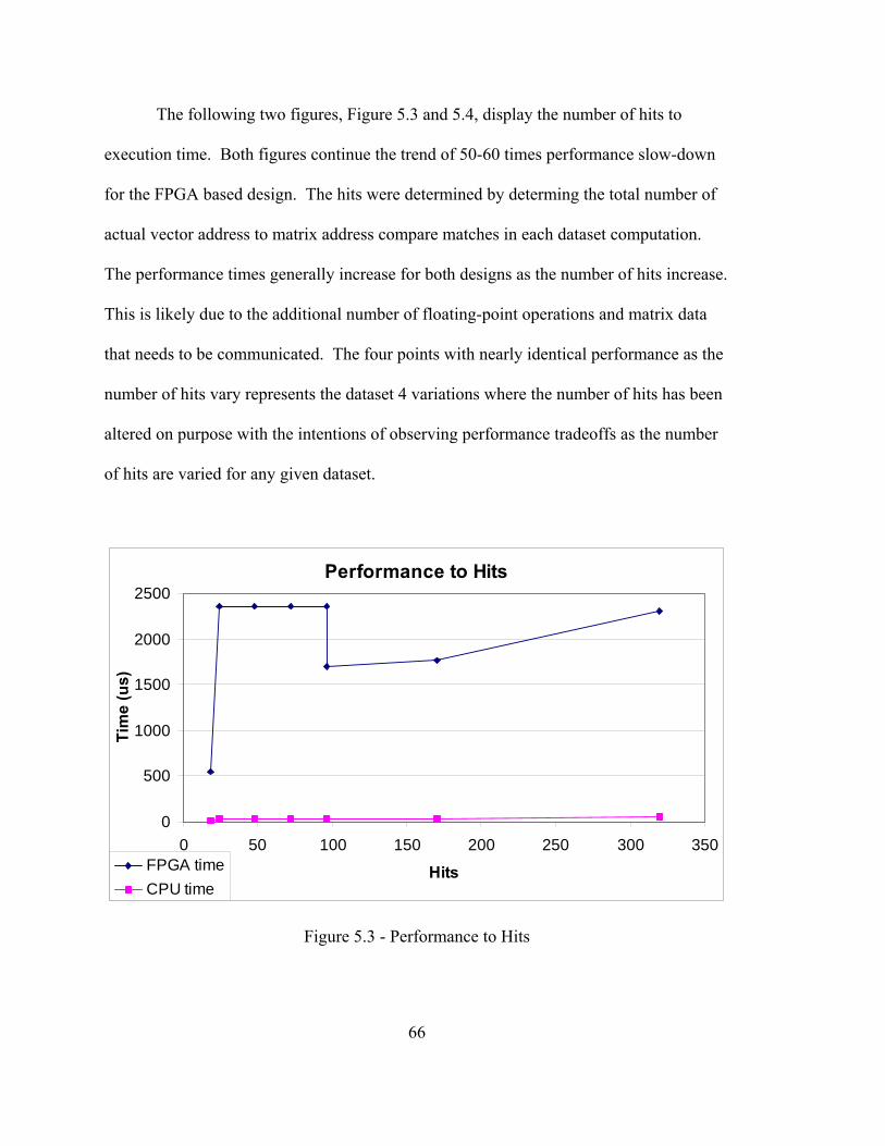
The following two figures, Figure 5.3 and 5.4, display the number of hits to
execution time. Both figures continue the trend of 50-60 times performance slow-down
for the FPGA based design. The hits were determined by determing the total number of
actual vector address to matrix address compare matches in each dataset computation.
The performance times generally increase for both designs as the number of hits increase.
This is likely due to the additional number of floating-point operations and matrix data
that needs to be communicated. The four points with nearly identical performance as the
number of hits vary represents the dataset 4 variations where the number of hits has been
altered on purpose with the intentions of observing performance tradeoffs as the number
of hits are varied for any given dataset.
Performance to Hits
0
500
1000
1500
2000
2500
0 50 100 150 200 250 300 350
Hits
Tim
e (u
s)
FPGA timeCPU time
Figure 5.3 - Performance to Hits
66
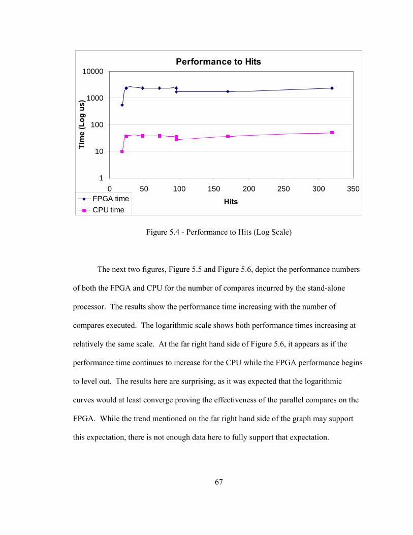
Performance to Hits
1
10
100
1000
10000
0 50 100 150 200 250 300 350
Hits
Tim
e (L
og u
s)
FPGA timeCPU time
Figure 5.4 - Performance to Hits (Log Scale)
The next two figures, Figure 5.5 and Figure 5.6, depict the performance numbers
of both the FPGA and CPU for the number of compares incurred by the stand-alone
processor. The results show the performance time increasing with the number of
compares executed. The logarithmic scale shows both performance times increasing at
relatively the same scale. At the far right hand side of Figure 5.6, it appears as if the
performance time continues to increase for the CPU while the FPGA performance begins
to level out. The results here are surprising, as it was expected that the logarithmic
curves would at least converge proving the effectiveness of the parallel compares on the
FPGA. While the trend mentioned on the far right hand side of the graph may support
this expectation, there is not enough data here to fully support that expectation.
67
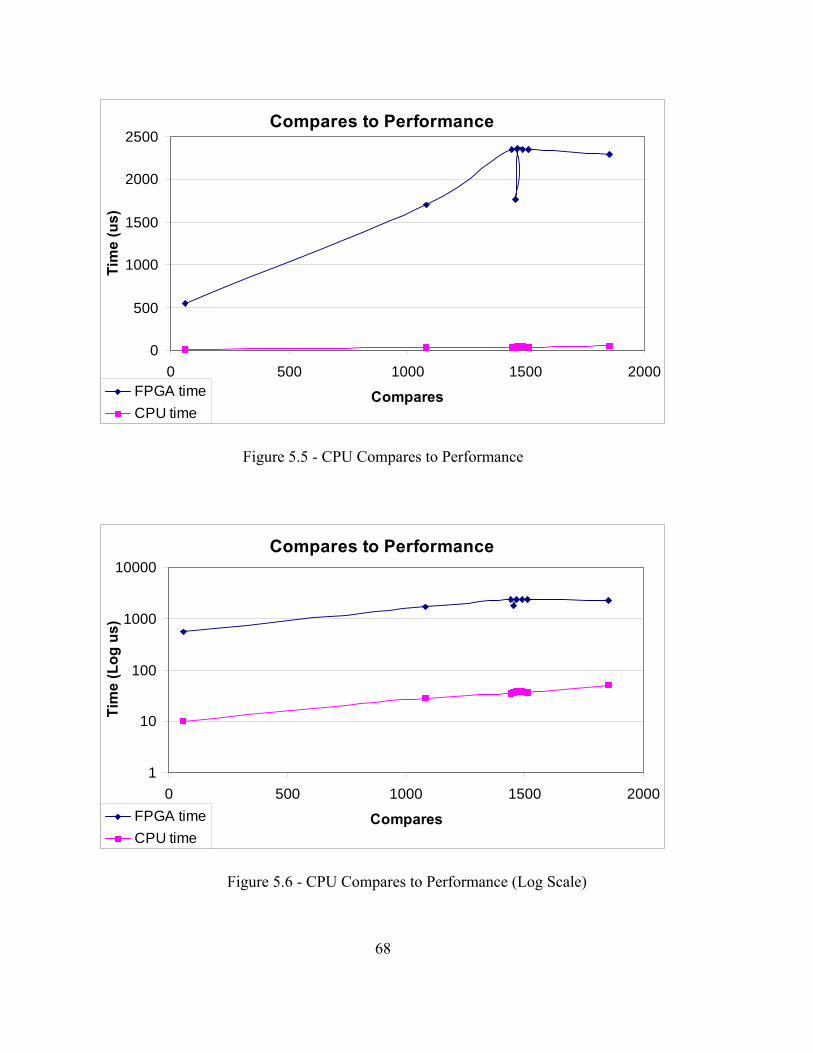
Compares to Performance
0
500
1000
1500
2000
2500
0 500 1000 1500 2000
Compares
Tim
e (u
s)
FPGA timeCPU time
Figure 5.5 - CPU Compares to Performance
Compares to Performance
1
10
100
1000
10000
0 500 1000 1500 2000
Compares
Tim
e (L
og u
s)
FPGA timeCPU time
Figure 5.6 - CPU Compares to Performance (Log Scale)
68
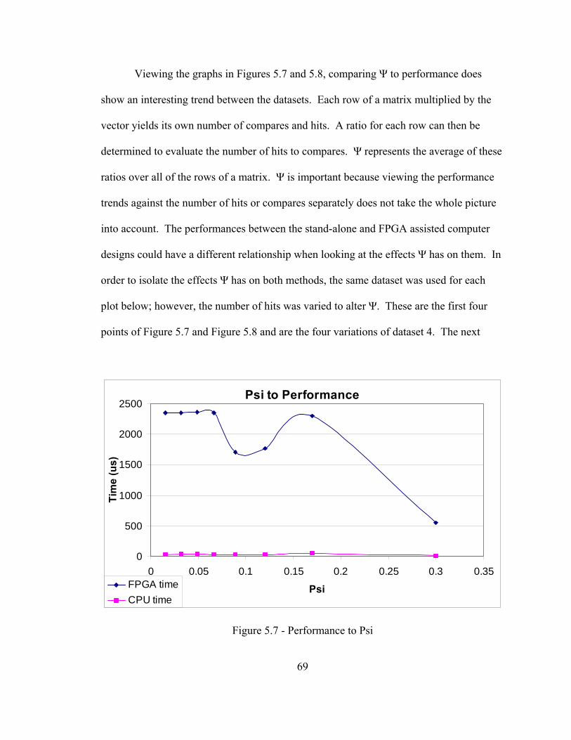
Viewing the graphs in Figures 5.7 and 5.8, comparing Ψ to performance does
show an interesting trend between the datasets. Each row of a matrix multiplied by the
vector yields its own number of compares and hits. A ratio for each row can then be
determined to evaluate the number of hits to compares. Ψ represents the average of these
ratios over all of the rows of a matrix. Ψ is important because viewing the performance
trends against the number of hits or compares separately does not take the whole picture
into account. The performances between the stand-alone and FPGA assisted computer
designs could have a different relationship when looking at the effects Ψ has on them. In
order to isolate the effects Ψ has on both methods, the same dataset was used for each
plot below; however, the number of hits was varied to alter Ψ. These are the first four
points of Figure 5.7 and Figure 5.8 and are the four variations of dataset 4. The next
Psi to Performance
0
500
1000
1500
2000
2500
0 0.05 0.1 0.15 0.2 0.25 0.3 0.35
Psi
Tim
e (u
s)
FPGA timeCPU time
Figure 5.7 - Performance to Psi
69
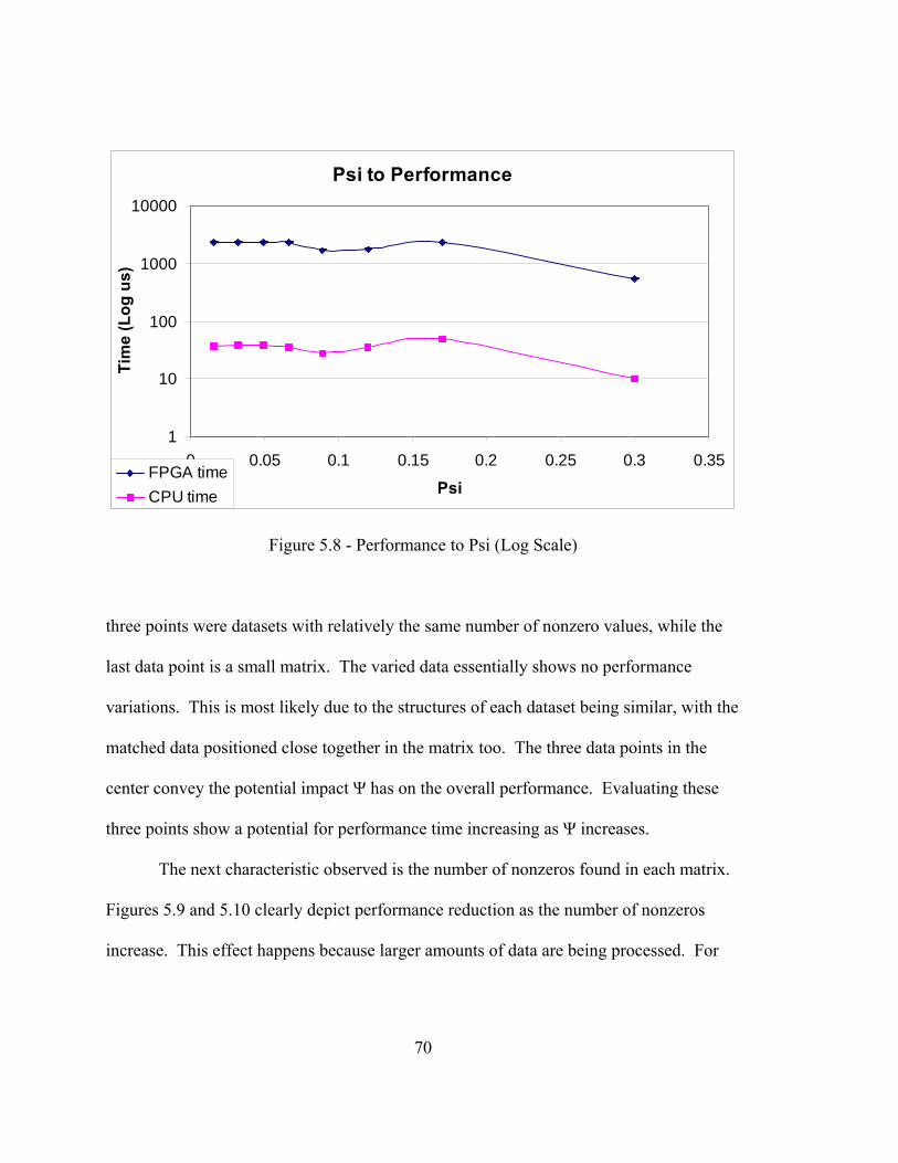
Psi to Performance
1
10
100
1000
10000
0 0.05 0.1 0.15 0.2 0.25 0.3 0.35
Psi
Tim
e (L
og u
s)
FPGA timeCPU time
Figure 5.8 - Performance to Psi (Log Scale)
three points were datasets with relatively the same number of nonzero values, while the
last data point is a small matrix. The varied data essentially shows no performance
variations. This is most likely due to the structures of each dataset being similar, with the
matched data positioned close together in the matrix too. The three data points in the
center convey the potential impact Ψ has on the overall performance. Evaluating these
three points show a potential for performance time increasing as Ψ increases.
The next characteristic observed is the number of nonzeros found in each matrix.
Figures 5.9 and 5.10 clearly depict performance reduction as the number of nonzeros
increase. This effect happens because larger amounts of data are being processed. For
70
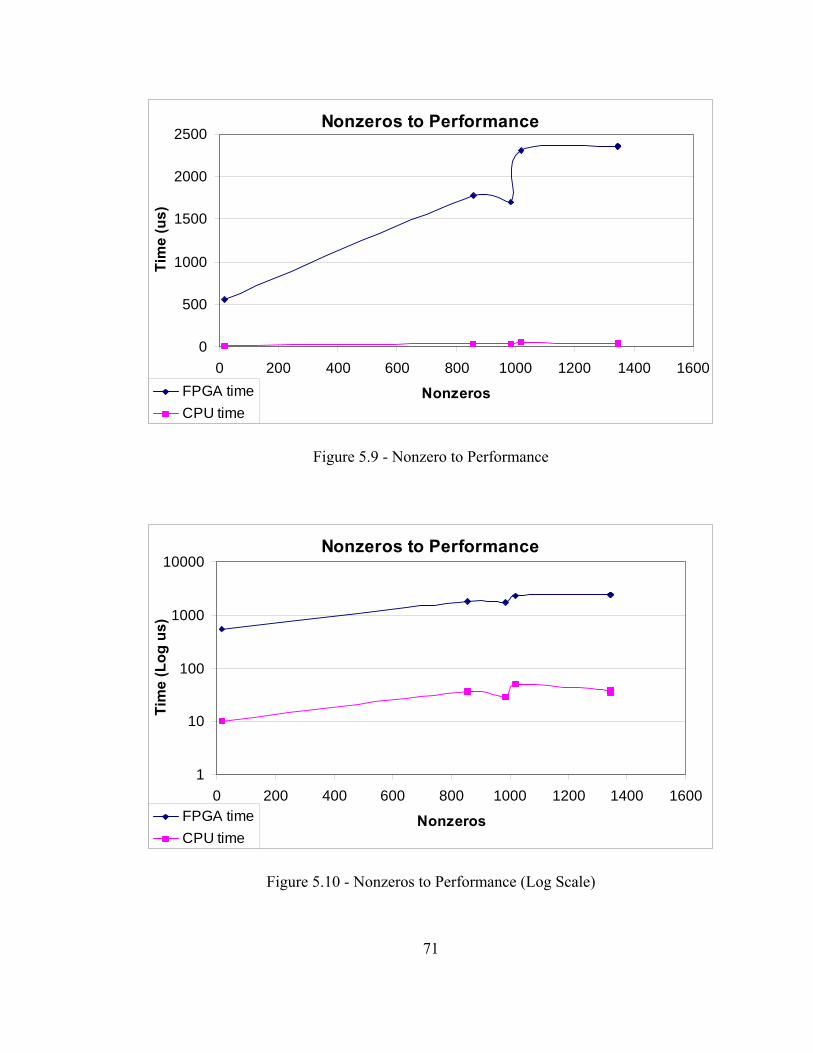
Nonzeros to Performance
0
500
1000
1500
2000
2500
0 200 400 600 800 1000 1200 1400 1600
Nonzeros
Tim
e (u
s)
FPGA timeCPU time
Figure 5.9 - Nonzero to Performance
Nonzeros to Performance
1
10
100
1000
10000
0 200 400 600 800 1000 1200 1400 1600
Nonzeros
Tim
e (L
og u
s)
FPGA timeCPU time
Figure 5.10 - Nonzeros to Performance (Log Scale)
71
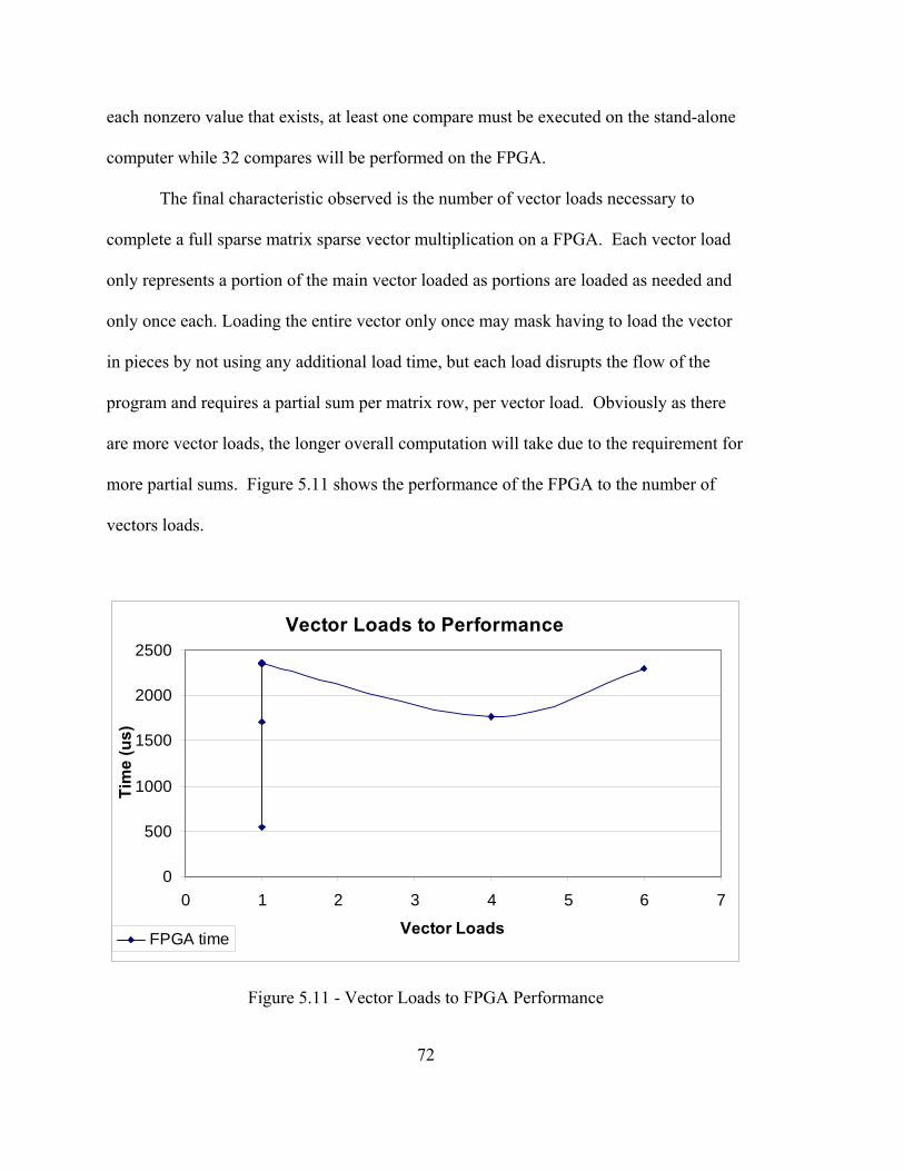
each nonzero value that exists, at least one compare must be executed on the stand-alone
computer while 32 compares will be performed on the FPGA.
The final characteristic observed is the number of vector loads necessary to
complete a full sparse matrix sparse vector multiplication on a FPGA. Each vector load
only represents a portion of the main vector loaded as portions are loaded as needed and
only once each. Loading the entire vector only once may mask having to load the vector
in pieces by not using any additional load time, but each load disrupts the flow of the
program and requires a partial sum per matrix row, per vector load. Obviously as there
are more vector loads, the longer overall computation will take due to the requirement for
more partial sums. Figure 5.11 shows the performance of the FPGA to the number of
vectors loads.
Vector Loads to Performance
0
500
1000
1500
2000
2500
0 1 2 3 4 5 6 7
Vector Loads
Tim
e (u
s)
FPGA time
Figure 5.11 - Vector Loads to FPGA Performance
72
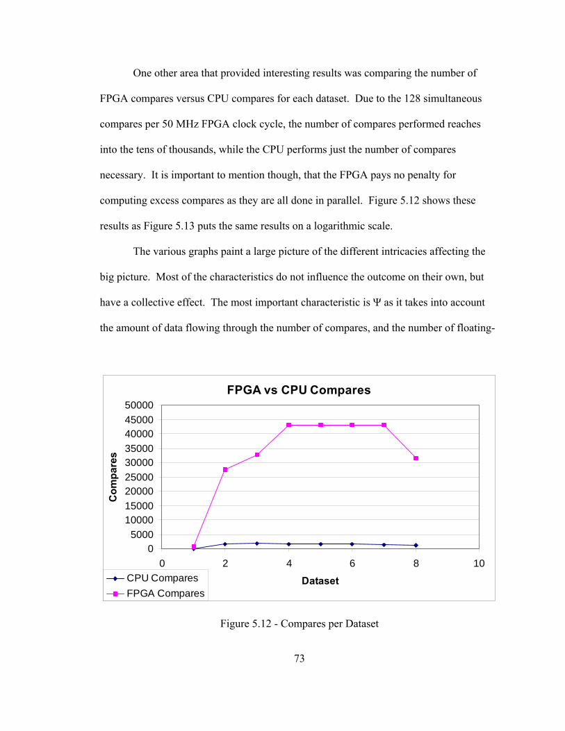
One other area that provided interesting results was comparing the number of
FPGA compares versus CPU compares for each dataset. Due to the 128 simultaneous
compares per 50 MHz FPGA clock cycle, the number of compares performed reaches
into the tens of thousands, while the CPU performs just the number of compares
necessary. It is important to mention though, that the FPGA pays no penalty for
computing excess compares as they are all done in parallel. Figure 5.12 shows these
results as Figure 5.13 puts the same results on a logarithmic scale.
The various graphs paint a large picture of the different intricacies affecting the
big picture. Most of the characteristics do not influence the outcome on their own, but
have a collective effect. The most important characteristic is Ψ as it takes into account
the amount of data flowing through the number of compares, and the number of floating-
FPGA vs CPU Compares
05000
100001500020000250003000035000400004500050000
0 2 4 6 8
Dataset
Com
pare
s
10CPU ComparesFPGA Compares
Figure 5.12 - Compares per Dataset
73

FPGA vs CPU Compares
1
10
100
1000
10000
100000
0 2 4 6 8
Dataset
Com
pare
s
10CPU ComparesFPGA Compares
Figure 5.13 - Compares per Dataset (Log Scale)
point operations that will be necessary to solve the problem due to hit quantity. Because
of this consequence, there is no single MFLOPS to be obtained. As Ψ will vary, the
actual MFLOPS or the percent of theoretical MFLOPS achieved will also vary. For
example, the third dataset has320 hits. The stand-alone CPU runs at 933 MHz; therefore,
its theoretical MFLOPS is 933. Its actual MFLOPS for this problem is 12.8. The
theoretical MFLOPS for the FPGA design is 150 while the actual MFLOPS is 0.278.
The percentage of the theoretical MFLOPS yielded is 1.07% and 0.19% for the stand-
alone and FPGA based designs respectively. Figures 5.14 and 5.15 display the variation
in percentage of theoretical MFLOPS achieved as Ψ varies.
When looking back over the graphs, the number of nonzero values plays a major
role in all of these results, for each nonzero value is processed through the designs.
74
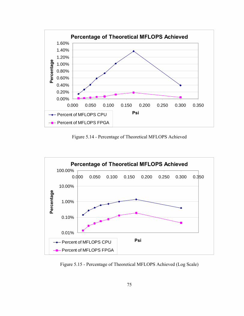
Percentage of Theoretical MFLOPS Achieved
0.00%0.20%0.40%0.60%0.80%1.00%1.20%1.40%1.60%
0.000 0.050 0.100 0.150 0.200 0.250 0.300 0.350
Psi
Perc
enta
ge
Percent of MFLOPS CPU
Percent of MFLOPS FPGA
Figure 5.14 - Percentage of Theoretical MFLOPS Achieved
Percentage of Theoretical MFLOPS Achieved
0.01%
0.10%
1.00%
10.00%
100.00%0.000 0.050 0.100 0.150 0.200 0.250 0.300 0.350
Psi
Perc
enta
ge
Percent of MFLOPS CPU
Percent of MFLOPS FPGA
Figure 5.15 - Percentage of Theoretical MFLOPS Achieved (Log Scale)
75
What needs to be taken into perspective is that when comparing results, the number of
nonzero values must be taken into consideration. If the amount of nonzero values’
addresses is relatively the same in comparing results across datasets, the results should
allow for comparison between other characteristics. If the number of nonzero values is
not relatively the same, then the results cannot be compared. The next sections discuss
the difficulties involved.
5.2 Difficulties
Several areas of difficulty were encountered in the development of the sparse
matrix sparse vector computation engine. The areas included developing a proper
interface from the FPGA back out to the C code, to memory and I/O limitations, and a
minor glitch.
5.2.1 Pcore Interface
An extremely large amount of time was spent in this single area alone of
developing a consistently working Pcore interface to connect the sparse matrix sparse
vector multiplication code to the memory bus. Roughly 33% of the design time was
spent creating and adjusting a Pcore interface to adequately support the overall design.
The Pcore interface must monitor data traffic on two different clock speeds between the
memory bus (100 MHz) and the sparse matrix sparse vector multiplication code (50
MHz). The synchronization of data between the two different clocks presented the
greatest challenge. There is no guarantee there will be a consistent stream of data with the
memory bus; therefore, the Pcore interface must be very versatile as well as fast. To
further increase the difficulty of this task, the Pilchard System’s design does not lend
itself to post-layout simulation, a key stage in the design process where the designer can
76
get a much more realistic view of how a design will work in reality, versus the perfect
world of presynthesis simulation. Pcore designs ranged from using block RAM as the
main device for interfacing to the memory bus, to relying on the handshaking read/write
signals to grab and send data appropriately. Various combinations of designs were
implemented with varying ranges of success. Often this part of the design drove the
overall clock speed of the design as whole. This is because the pcore needs to be twice as
fast as the rest of the FPGA so it could properly supply twice the amount of data (128
bits) as the memory bus (64 bits) in one 50 MHz clock cycle. The final design involved
using an asynchronous FIFO buffer created by Xilinx’s Corgen to handle the movement
of data between the two different clock speeds. A small (4 address locations) block RAM
was used for data leaving the FPGA to the memory bus to read.
5.2.2 Memory and I/O Constraints
The constraints the memory and I/O limitations held on the design dominated the
performance of the FPGA assisted sparse matrix sparse vector multiplication results.
These limitations ranged from space on the FPGA, to FPGA slice usage, to a lack of
RAM on the Pilchard System board to supply this data hungry design with information as
fast as possible.
When possible, Xilinx Coregen components were utilized to help save space and
time in the FPGA design; however, this was not always enough. Originally the FPGA
was to hold a vector of size 64 and perform 256 simultaneous compares. Unfortunately,
doing so utilized 87% of the FPGA’s slices when combined with the rest of the design.
Attempting to completely place and route a design with the usage of slices reaching over
75% becomes difficult, not even considering the small likelihood of meeting timing
77
constraints. To alleviate this limitation, the onboard vector size was cut back to 32, thus
reducing the total number of simultaneous compares to 128 in one clock cycle. The
vector data was also moved to block RAM from registers. The slice usage dropped to
70% of the FPGA’s available 12,288 slices. This was enough to allow the design to be
place and routed at the necessary timing constraints. The effects of reducing the vector
size on performance in presynthesis simulation were felt immediately as simulation times
nearly doubled. The effects on the actual FPGA was never observed due to the larger
design never being able to be place and routed.
Lastly, due to the need for the FPGA to have constant and quick access to large
amounts of data, the use of onboard RAM on the Pichard would have been very
beneficial. The FPGA must grab data from the main memory (RAM) on the CPU, which
is a very time consuming operation when typical programs can utilize cache. The
availability of RAM on the Pilchard board would not only act similar to cache, but it
would also give the FPGA the ability to have the entire vector stored nearby instead of
some location off in the main memory. This would eliminate time lost for memory bus
contention. Also, large amounts of the matrix could be stored and possibly the entire
vector. This reduction in the use of the memory bus would reduce the communication
cost incurred essentially over the entire design execution time.
The one single factor that potentially had the largest effect was the result of the
I/O constraints. The design is highly dependent upon the I/O or memory bus due to the
large amounts of data transfer. A small test was conducted to measure the time to
perform 10 writes to get an estimate of how much time is spend on I/O in the overall
design. This test concluded that 10 writes would take 4.5us. Simulation provided
78
accurate results but the implementation of the Pilchard System Wrapper could not
accurately be simulated nor could a memory bus be accurately simulated; however, the
execution time estimated by the simulator painted a much different picture. If dataset 3
was considered, the FPGA execution time was 2300us. By determining the number of
writes and using the small test data, it was determined that 30% of that execution time
was spent conducting I/O. While this seems underestimated and the small test is likely
inaccurate when referring to a larger design, the simulation results estimated that the
design should be executed in 53us, a 97% improvement. At the very least, I/O
performance has a huge impact on the design whether that be 30 to 97% of the execution
time.
While performance results did not meet the desired goals, it is clear what is
necessary to alleviate these problems through larger FPGA’s, multiple FPGA’s, improved
interfacing, and onboard RAM. These suggestions for improvements with further details
can be found in the next chapter, Conclusions and Future Work.
5.2.3 Logic Glitch
Through the various tests run on the FPGA design, a minor flaw in the logic was
exposed. Fortunately this glitch has no effect on performance or accuracy when the
FPGA produces results. The flaw was identified as the FPGA logic not synchronizing
correctly with the host C code when a set of compares produced no hits for a partial sum;
thus yielding a partial sum of zero. Currently, several conditions must be met for a zero
partial sum to occur and these conditions are all not being met. When this occurs, the
FPGA essentially locks into the SEND state. Extensive simulation never brought this
situation to light when using the same test data that would cause the error in real-time
79

calculations on the FPGA; thus underlining the importance of post-synthesis and post-
layout simulation capabilities. Due to the specific nature of this issue, it can be
efficiently resolved by creating a process on the FPGA to monitor if hits ever occur
during a partial sum. It no hits ever occur, the C code and FPGA will not expect nor send
a zero partial sum respectively, and both will move on to the next appropriate state. This
method would eliminate a list of conditions that need to be met by the current
architecture.
80
Chapter 6
Conclusions and Future Work
In hindsight, the overall design was successful in the fact that results were
achieved with data from which to extrapolate and learn from sparse matrix sparse vector
multiplication on a FPGA. When comparing the performance to the stand-alone
processor, a significant gap in performance must be corrected and improved upon. The
following chapter will discuss future work by analyzing areas of improvement and
interesting applications to apply this design to. Finally, conclusions will be given
encapsulating the entire experience.
6.1 Hardware Improvements
A few areas are available to improve from the hardware side of the system. The
Pilchard System is aging; new Xilinx Virtex-II Pro FPGAs are larger, faster, and have
optional PowerPC processors on board, and/or onboard memory or cache could be added
to the system. The Pilchard System was designed to operate on a 133 MHz memory bus;
however, today’s computers have much faster memory buses with speeds of up to 800
MHz [18]. The Pilchard System could not take advantage of today’s bus speeds. If the
overall system hardware was upgraded, several innovations could play an immense role
without the sparse matrix sparse vector design even changing. If the bus was dedicated to
the FPGA’s needs and running at a speed of 800 MHz, the bus could theoretically support
up to 8 FPGAs all running at 100 MHz assuming the Pilchard board would be compatible
or if it were upgraded.
81
Upgrading the FPGA could play a significant role in improvement as well. If a
board using a Xilinx Virtex-II Pro X were placed on one of the latest computers,
speedups and improvements would be found in several areas. Xilinx Virtex-II Pro X
XC2VPX70 has almost three times the number of slices (33,088) as the Virtex 1000-E
(12,288 slices and 4Kbits of block RAM) and has 5.5Mb of dual port block RAMs
available allowing for significant upgrades in vector storage size, concurrent compares,
and vector data storage. With that much block RAM available; it is even possible that the
entire vector and even small to midsize sparse matrices could be stored on the FPGA at
the very least. The optional PowerPCs could also be used on the latest Virtex-II Pro X
FPGAs to assist in the overall control or various other areas. With this single
improvement in FPGA size, the vector size stored on the FPGA and number of parallel
compares could at least be tripled if the rest of the design remains intact. This estimation
is based on an earlier design that had twice the current vector size stored and double the
number of compares, and the design was only over-mapped by only 4-5,000 slices.
Simulation times improved almost 40% when twice the current number of compares and
vector storage was implemented.
Another benefit in being able to store more if not the entire vector on the FPGA
and possibly the matrix is that the memory bus would only be needed at the beginning of
execution to load all of the information onto the FPGA. As mentioned in the previous
chapter, the I/O communication cost of the memory bus is potentially consuming 30 to
97% of execution time. Having onboard RAM or cache on the pilchard board, or another
similar type board would create the same improvements in eliminating as much of the
memory bus dependency as possible. Having onboard RAM would likely be very large
82
in comparison to the FPGA’s RAM (32 – 128 Mb) and could quite possibly store all
necessary matrix and vector data.
If upgrading the Pilchard System is not an option, at the very least more than one
Pilchard System could be placed on a computer with a faster bus speed so more FPGA
resources are available to improve overall performance (again assuming the Pilchard
Board could operate on a faster bus). If the Pilchard System was no longer usable the
design, excluding the Pcore interface, could be fitted onto another system where more
FPGA resources are available. The Pcore interface is specific to the Pilchard System;
therefore, a new interface would have to be developed for any new system the design is
placed on. While hardware improvements are not always easy to accommodate due to
economics, design improvements can still be made.
A final hardware improvement would be for the Pilchard Board to be on a bus
utilizing some sort of DMA Controller. Currently the Pilchard must compete for the
memory bus like every other process running on the main computer. This can create
unknown and unpredictable data transfer times, not to mention increased communication
costs. If a DMA was used, the controller could gain access of the bus and be able to send
dedicated block transfers of data to the FPGA without so much interruption, again further
reducing I/O costs.
6.2 FPGA Architecture Improvement
An architectural improvement in the design or layout of processes on the FPGA
would be to add the capability of allowing multiple configurations based on the structure
of the sparse matrix. This analysis and design would require pre-processing which could
be done on the FPGA or software side and would likely require a fair amount of research
83
into how this could be efficiently implemented, but having the ability to cater to how the
FPGA solves a structured matrix would be beneficial to overall performance provided
that the preprocessing step did not outweigh the improvement. Sometimes sparse matrix
sparse vector multiplications are run multiple times for example in executing some
iterative solvers. If the FPGA could adapt by monitoring the Ψ, after the first run, the
design could adjust by possibly utilizing more MACs if the Ψ value was large (0.6 to 1.0
possibly). This would be assuming more MAC units could fit on the FPGA.
6.3 Algorithmic Improvements
In the creation and design of the sparse matrix sparse vector multiplication,
several important areas have opened up to improve efficiency and overall performance by
reducing the amount of inactivity during waiting, improving data accuracy, and not
wasting clock cycles handling unnecessary information. These algorithmic
improvements include only grabbing vector values as needed and then storing them if
needed again, loading up the next compare results while waiting on an answer from the
multiply accumulator, adding full IEEE 754 support for floating point numbers, keeping
track of multiple partial sums simultaneously, and reducing the number of pipeline stages
in the floating point units.
An algorithm that only requested and stored vector values as needed could
possibly be implemented over the existing model with only incurring the penalty of one
extra sparse code clock cycle per REPORTx state encountered. This extra clock cycle
would be needed to encode a request to the C program to send a vector value or values
with the matched matrix values. To handle this on the FPGA side, each vector slot would
have a status bit of whether it had the value available for a particular address or not. The
84
check for the existing vector value could be done in the same processes as the current
compare processes if the overall speed is not slowed down, or it could be handled in
separate processes. The only difficulty in handling this approach would be keeping track
of matrix and vector values when streaming them into the multipliers. All that should be
necessary is to predetermine an algorithm that would handle expected ordering of the
values sent on the FPGA side and implemented by the C program. The improvements
seen by this scheme would be every time a startup cost is incurred of reloading the
vector. The best-case scenario for the improvement would be that 2 out of every 3 clock
cycles during a vector load would be saved per vector value not ever needed. As is
typical, the more dense the matrix and vector, the less of an improvement that will be
observed; however this improvement while not helping the worst-case scenario, would
help the best-case scenario of an extremely sparse matrix and vector. The cost of sending
the vector value with the matrix values is no different than preloading it. Again, this
method would reduce costly I/O as has been shown to be a large problem.
Another improvement to the algorithm of the system would be improving the
overall system efficiency while waiting for an answer from the FPGA code. Currently
while the FPGA code is determining a partial sum after an over flag has gone high, the C
program waits for the answer, which could take about 1 to 1.5 microseconds (according
to simulation times) if waiting on a partial sum after a set of compare matches. During
this time the FPGA could send in the next row’s matrix addresses to begin the next round
of compares. If the partial sum were to be found during this time, the FPGA could
simply wait until after the address data has been streamed in for comparing. A special
case to take care of here is if there were no matches to be calculated into the current
85
partial sum, it is possible the partial sum could already be ready; therefore, in this case
the C program should just wait on the partial sum. This improvement could help both the
best and worst-case scenarios.
Adding full IEEE 754 support into the floating-point units would be beneficial in
that the usefulness of this design for scientific use would be more practical. While
improving the floating-point units, they could both be analyzed to see if any of the
existing pipeline stages could be consolidated. Typically the more pipeline stages, the
faster the component, but if the speed can be maintained while reducing pipeline stages,
the overall latency when waiting for a result is reduced. In particular, consolidating the
adder pipeline would shave clock cycles off finding the partial sum as that is a bottleneck
in the overall design due to the adder having to wait on itself for 13 clock cycles for a
result if the last two pieces of data to be summed are not available at the same time.
The last algorithmic improvement involves the continued improvement over the
adder bottleneck. As the number of results run low for the adder to put together for a
partial sum, the adder may only have a couple of additions in the pipeline while another
piece of data waits on results. The adder is in use, but the pipeline is becoming a
hindrance instead of a benefit. To help mask this problem, giving the multiply
accumulator the ability to handle multiple partial sums would help immensely. Creating
this improvement would automatically improve some other areas too. To handle multiple
partial sums simultaneously, the overall system would need to just send in rows of
information and not have to wait for an answer like mentioned above. For the FPGA to
notify the C program that an answer is ready, it can do this by using a reserved bit of the
output vector during the REPORTx stage. Also, the remaining 3 bits could be used to
86
signal that up to 8 answers are available; therefore, up to 8 partial sums could be the limit
supported (000 would stand for 1, since the answer flag must be high to signal that any
results are available). This improvement would definitely require further analysis as
supporting 8 partial sums could overload the existing single adder requiring the addition
of one or more addition units. The downside to this approach is determining how an
adder knows which set of data that is currently being considered for addition goes to
which partial sum. A buffer that mirrors the data buffer would likely be used that stands
for the partial sum that data corresponds to. Implementing this could be very complex
yet very beneficial.
6.4 Future Applications
In addition to improvements that could be made on the existing system, the
overall approach could be applied to new problems or altered for different applications.
Some of these different applications would be applying the design to sparse matrix sparse
matrix multiplication problems, altering the design to only handle compares, or reading in
multiple rows of a matrix instead of multiple elements from one row. Altering the design
to handle only comparisons could have a unique impact on the overall problem.
Essentially, the only involvement of the FPGA would be to read in vector and matrix
addresses, compare them, and send out the results in some encoded fashion. No multiply
accumulation would be handled on the FPGA. While this greatly simplifies the amount
of work done on the FPGA it also further complicates the work of the C program.
Unfortunately for the C program, it must compete with an operating system and possibly
other programs. The FPGA only has to worry about itself once it has the data necessary
87
to process. As has been observed the overhead of transferring and partial summing all of
the floating-point data is costly.
Another application of this design would be to transfer addresses of the matrix
two to multiple rows at a time. This would require the ability to handle partial sums. The
performance results could have some intriguing affects when compared to the original
algorithm. A problem with this method; however, is if one row is ready for a new vector
to be loaded while other rows are not ready.
A final and more practical application would involve the exploration of applying
this design to the calculation of sparse matrix sparse matrix multiplication. The basis for
sparse matrix sparse matrix multiplication is essentially sparse matrix sparse vector
multiplication repeated for each vector of the second matrix. This application could be
divided on multiple computers using the Pilchard System over a network. The load could
be distributed by one row of the second matrix per computer or it could be broken down
further into each computer gets a portion of a vector per row of the second matrix.
There are numerous possibilities to improve upon the existing design and to apply
it new areas in computing for improved performance results.
6.5 Conclusion
In evaluating the entire design process, design, and results a lot has been learned
about sparse matrix sparse vector multiplication on parallel and reconfigurable
computing. When evaluating results from this problem various different characteristics
of the sparse matrix and vector affect the outcome. When viewing results, the number of
nonzeros must always be taken into consideration as well when comparing to other
88
results. The potential influence Ψ has on performance with how it measures the number
of compares and hits regarding performance time are important too.
The importance of being able to perform post-synthesis and post-layout simulations
was reinforced too. When attempting to troubleshoot problems that did not appear in
simulation, determining what exactly is going wrong in the chip is extremely difficult and
it is hard to know if processes sharing data over different clock rates are synchronizing
correctly. A lot of time spent troubleshooting errors could conceivably have been saved
if this capability was available.
Even though FPGA performance results were slower than the stand-alone computer’s
performance by 50-60 times, it is worth continued research in this area for several
reasons. First not much research as been conducted or at least published regarding sparse
matrix sparse vector multiplication using FPGA’s, and this one approach certainly
doesn’t cover all of the possibilities of implementations; however, it does take a
performance minded approach and discusses several possibilities for improvements. Due
to the largest bottleneck being the heavy performance cost paid for memory bus
communication and contention as well as memory constraints, the design could actually
be extremely competitive if not faster to the stand-alone computer’s performance. As
was mentioned in the previous chapter, simulation times were extremely close to that of
the actual performance times on the stand-alone computer’s results. Add in more FPGA
room and the potential performance improvement is quite optimistic. Exploring these
external limitations to the design’s performance is a must. In addition to external
limitations, there are also design improvements that can still be made as mentioned
earlier in the chapter.
89

In summary, being a pioneer in this particular application of the sparse matrix sparse
vector multiplication, much has been learned but plenty of research remains in exploring
this topic. Its importance is felt in the scientific computing community and could
therefore take advantage of performance improvements resulting from continued research
in this field.
90

References
91
References
1. The Message Passing Interface Standard (2004). http://www-unix.mcs.anl.gov/mpi/mpich/
2. Parallel Virtual Machine (2004). http://www.csm.ornl.gov/pvm/pvm_home.html 3. Institute for Electrical and Electronics Engineers. IEEE 754 Standard for Binary
Floating-Point Arithmetic, 1985. 4. K.H. Tsoi. Pilchard User Reference (V0.1), Department of Computer Science
and Engineering, The Chinese University of Hong Kong, Shatin, NT Hong Kong, January 2002.
5. K. A. Gallivan. Set 2 – Sparse Matrix Basics. School of Computational Science and Information Technology, Florida State University,2004. http://www.csit.fsu.edu/~gallivan/courses/NLA2/set2.pdf
6. K. L. Wong. Iterative Solvers for System of Linear Equations. Joint Institute for Computational Science. 1997.
7. D. W. Bouldin. Lecture Notes: Overview, ECE 551, Electrical and Computer Engineering Department, University of Tennessee, 2002.
8. N. Shirazi, A. Walters, and P. Athanas. Quantitative Analysis of Floating Point Arithmetic on FPGA Based Custom Computing Machines. EEE Symposium on FPGAs for Custom Computing Machines, Napa, California, Apr 1995.
9. G. Lienhart, A. Kugel, and R. Männer. Using Floating-Point Arithmetic on FPGAs to Accelerate Scientific N-Body Simulations. Proceedings, IEEE Symposium on Field-Programmable Custom Computing Machines, pages 182–191, Napa, CA, Apr. 2002.
10. H. ElGindy, Y. Shue. On Sparse Matrix-Vector Multiplication with FPGA-Based System. Proceedings of the 10 th Annual IEEE Symposium on Field-Programmable Custom Computing Machines (FCCM'02), p.273, September 22-24, 2002 .
11. Netlib Repository. The University of Tennessee, Knoxville and Oak Ridge National Laboratories, www.netlib.org.
12. G. Wellein, G. Hager, A. Basermann, and H. Fehske. Fast sparse matrix-vector multiplication for TeraFlop/s computers. In High Performance Computing for Computational Science - VECPAR 2002, Lecture Notes in Computer Science, pages 287-301. Springer, 2003.
13. W. Gropp, D. Kaushik, D. Keyes, and B. Smith. Improving the performance of sparse matrix-vector multiplication by blocking. Technical report, MCS Division, Argonne National Laboratory. www-fp.mcs.anl.gov/petsc-fun3d/Talks/multivec_siam00_1.pdf.
14. R. Geusand and S. Röllin. Towards a fast parallel sparse matrix-vector multiplication. Proceedings of the International Conference on Parallel Computing (ParCo), pages 308.315. Imperial College Press, 1999.
15. F. Khoury. Efficient Parallel Triangular System Solvers for Preconditioning Large Sparse Linear Systems. Honour’s Thesis, School of Mathematics, University of New South Wales. http://www.ac3.edu.au/edu/papers/Khoury-thesis/thesis.html,1994.
92

16. Xilinx, www.xilinx.com. 17. D. E. Culler, J. P. Singh, and A. Goopta. Parallel Computer Architecture: A
Hardware/Software Approach. Morgan Kaufman Publishers, Inc., San Francisco: 1999.
18. Dell Computer Corporation, www.dell.com.
93

Appendices
94

Appendix A – Dataset Statistics
95
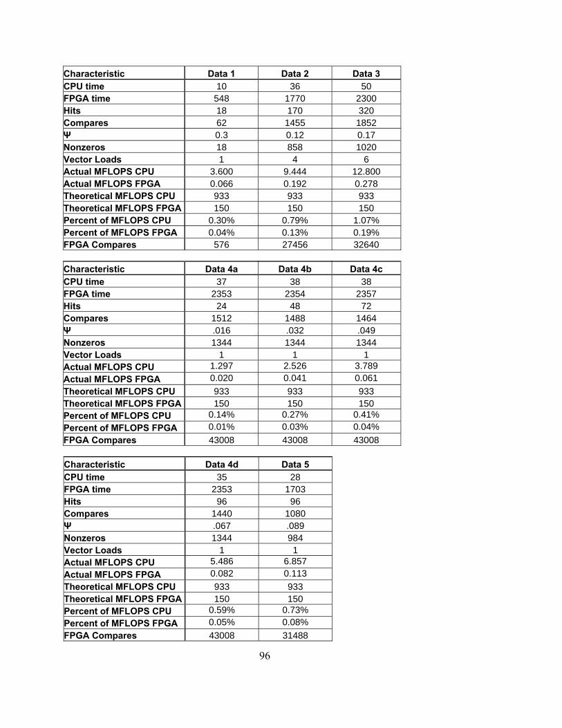
Characteristic Data 1 Data 2 Data 3 CPU time 10 36 50 FPGA time 548 1770 2300 Hits 18 170 320 Compares 62 1455 1852 Ψ 0.3 0.12 0.17 Nonzeros 18 858 1020 Vector Loads 1 4 6 Actual MFLOPS CPU 3.600 9.444 12.800 Actual MFLOPS FPGA 0.066 0.192 0.278 Theoretical MFLOPS CPU 933 933 933 Theoretical MFLOPS FPGA 150 150 150 Percent of MFLOPS CPU 0.30% 0.79% 1.07% Percent of MFLOPS FPGA 0.04% 0.13% 0.19% FPGA Compares 576 27456 32640 Characteristic Data 4a Data 4b Data 4c CPU time 37 38 38 FPGA time 2353 2354 2357 Hits 24 48 72 Compares 1512 1488 1464 Ψ .016 .032 .049 Nonzeros 1344 1344 1344 Vector Loads 1 1 1 Actual MFLOPS CPU 1.297 2.526 3.789 Actual MFLOPS FPGA 0.020 0.041 0.061 Theoretical MFLOPS CPU 933 933 933 Theoretical MFLOPS FPGA 150 150 150 Percent of MFLOPS CPU 0.14% 0.27% 0.41% Percent of MFLOPS FPGA 0.01% 0.03% 0.04% FPGA Compares 43008 43008 43008 Characteristic Data 4d Data 5 CPU time 35 28 FPGA time 2353 1703 Hits 96 96 Compares 1440 1080 Ψ .067 .089 Nonzeros 1344 984 Vector Loads 1 1 Actual MFLOPS CPU 5.486 6.857 Actual MFLOPS FPGA 0.082 0.113 Theoretical MFLOPS CPU 933 933 Theoretical MFLOPS FPGA 150 150 Percent of MFLOPS CPU 0.59% 0.73% Percent of MFLOPS FPGA 0.05% 0.08% FPGA Compares 43008 31488
96
Appendix B – Sparse Matrix Sparse Vector Multiplication C Code
97
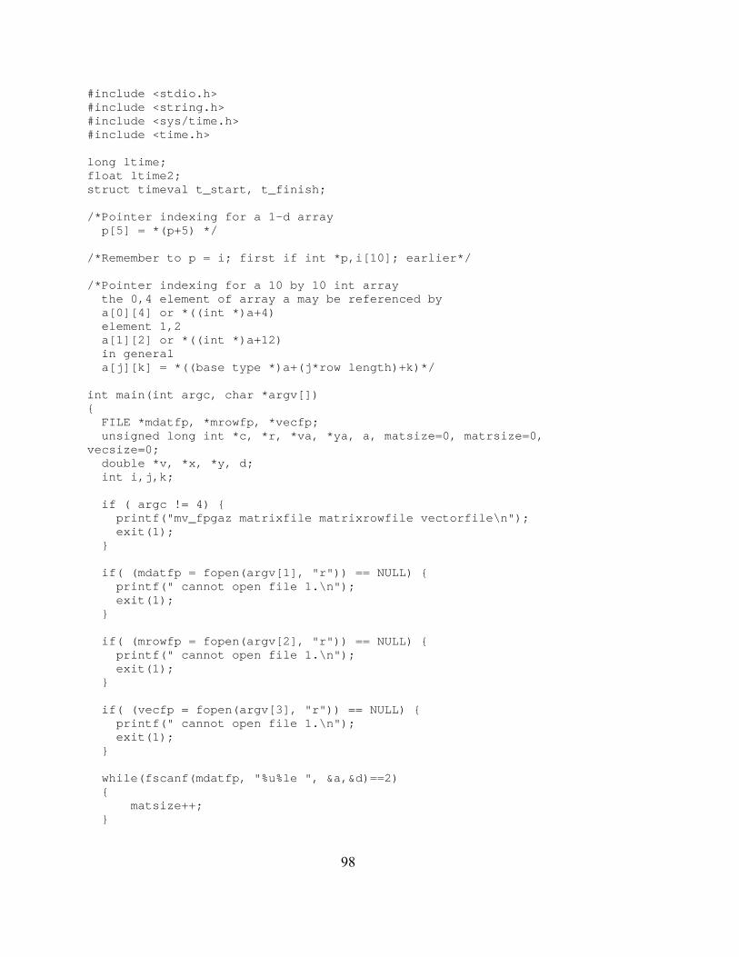
#include <stdio.h> #include <string.h> #include <sys/time.h> #include <time.h> long ltime; float ltime2; struct timeval t_start, t_finish; /*Pointer indexing for a 1-d array p[5] = *(p+5) */ /*Remember to p = i; first if int *p,i[10]; earlier*/ /*Pointer indexing for a 10 by 10 int array the 0,4 element of array a may be referenced by a[0][4] or *((int *)a+4) element 1,2 a[1][2] or *((int *)a+12) in general a[j][k] = *((base type *)a+(j*row length)+k)*/ int main(int argc, char *argv[]) { FILE *mdatfp, *mrowfp, *vecfp; unsigned long int *c, *r, *va, *ya, a, matsize=0, matrsize=0, vecsize=0; double *v, *x, *y, d; int i,j,k; if ( argc != 4) { printf("mv_fpgaz matrixfile matrixrowfile vectorfile\n"); exit(1); } if( (mdatfp = fopen(argv[1], "r")) == NULL) { printf(" cannot open file 1.\n"); exit(1); } if( (mrowfp = fopen(argv[2], "r")) == NULL) { printf(" cannot open file 1.\n"); exit(1); } if( (vecfp = fopen(argv[3], "r")) == NULL) { printf(" cannot open file 1.\n"); exit(1); } while(fscanf(mdatfp, "%u%le ", &a,&d)==2) { matsize++; }
98

while(fscanf(mrowfp, "%u", &a)==1) { matrsize++; } while(fscanf(vecfp, "%u%le ", &a,&d)==2) { vecsize++; } rewind(mdatfp); rewind(mrowfp); rewind(vecfp); c = (unsigned long int *)malloc(matsize * sizeof(unsigned long int) ); v = (double *)malloc(matsize * sizeof(double) ); r = (unsigned long int *)malloc(matrsize * sizeof(unsigned long int) ); x = (double *)malloc(vecsize * sizeof(double) ); va = (unsigned long int *)malloc(vecsize * sizeof(unsigned long int) ); y = (double *)malloc(matrsize * sizeof(double) ); ya = (unsigned long int *)malloc(matrsize * sizeof(unsigned long int) ); i=0; while(fscanf(mdatfp, "%u%le ", (c+i),(v+i))==2)i++; i=0; while(fscanf(mrowfp, "%u ",(r+i))==1)i++; i=0; while(fscanf(vecfp, "%u%le ", (va+i),(x+i))==2)i++; fclose(mdatfp); fclose(mrowfp); fclose(vecfp); gettimeofday(&t_start,NULL); for (i = 0; i < matrsize-1; i++) { *(y+i) = 0.0; k=0; for (j = *(r+i); j<*(r+i+1); j++) { if(*(c+j) < *(va+k))continue; else if(*(c+j) == *(va+k)) { *(y+i) = *(y+i) + *(v+j) * *(x+ k); k++; } else {
99
if(k<=vecsize) { for(k=k++;k<=vecsize-1;k++) { if(*(c+j) < *(va+k))break; else if(*(c+j) == *(va+k)) { *(y+i) = *(y+i) + *(v+j) * *(x+ k); break; } else { if(k<=vecsize)continue; else break; } } } else break; if(k<=vecsize) { if(*(c+j) < *(va+k))continue; else if(*(c+j) == *(va+k))continue; else break; } else break; } } } gettimeofday(&t_finish,NULL); ltime = (t_finish.tv_sec-t_start.tv_sec) * 1000000 + (t_finish.tv_usec-t_start.tv_usec); ltime2 = (float) ltime / 1; printf("CPU : calculation completed in %f usec\n",ltime2); for(i=0;i<matrsize-1;i++) { printf("--> %f\n",*(y+i)); } return 0; }
100

Appendix C – FPGA Host C Code
101
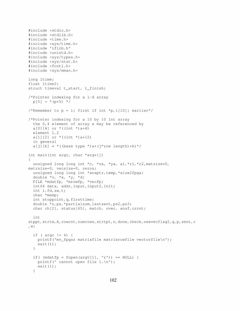
#include <stdio.h> #include <stdlib.h> #include <time.h> #include <sys/time.h> #include "iflib.h" #include <unistd.h> #include <sys/types.h> #include <sys/stat.h> #include <fcntl.h> #include <sys/mman.h> long ltime; float ltime2; struct timeval t_start, t_finish; /*Pointer indexing for a 1-d array p[5] = *(p+5) */ /*Remember to p = i; first if int *p,i[10]; earlier*/ /*Pointer indexing for a 10 by 10 int array the 0,4 element of array a may be referenced by a[0][4] or *((int *)a+4) element 1,2 a[1][2] or *((int *)a+12) in general a[j][k] = *((base type *)a+(j*row length)+k)*/ int main(int argc, char *argv[]) { unsigned long long int *c, *va, *ya, a1,*r1,*r2,matsize=0, matrsize=0, vecsize=0, zeros; unsigned long long int *ansptr,temp,*size2fpga; double *v, *x, *y, *d; FILE *mdatfp, *mrowfp, *vecfp; int64 data, addr,input,input2,init; int i,fd,sw,t; char *memp; int stoppoint,q,firsttime; double *z,ps,*partialsum,lastsent,ps2,ps3; char ch[2], status[65], match, over, ansf,crrnt; int stppt,strtm,A,rowcnt,numrows,strtpt,n,done,check,newvecflag2,g,p,sent,r,w; if ( argc != 4) { printf("mv_fpgaz matrixfile matrixrowfile vectorfile\n"); exit(1); } if( (mdatfp = fopen(argv[1], "r")) == NULL) { printf(" cannot open file 1.\n"); exit(1); }
102
if( (mrowfp = fopen(argv[2], "r")) == NULL) { printf(" cannot open file 1.\n"); exit(1); } if( (vecfp = fopen(argv[3], "r")) == NULL) { printf(" cannot open file 1.\n"); exit(1); } while(fscanf(mdatfp, "%u%le ", &a1,&d)==2) { matsize++; } while(fscanf(mrowfp, "%u ", &a1)==1) { matrsize++; } while(fscanf(vecfp, "%u%le ", &a1,&d)==2) { vecsize++; } rewind(mdatfp); rewind(mrowfp); rewind(vecfp); /*Matrix Column Address*/ c = (unsigned long long int *)malloc(matsize * sizeof(unsigned long long int) ); /*Matrix Value*/ v = (double *)malloc(matsize * sizeof(double) ); /*Matrix Row Pointer 1 & 2 */ r1 = (unsigned long long int *)malloc(matrsize * sizeof(unsigned long long int) ); r2 = (unsigned long long int *)malloc(matrsize * sizeof(unsigned long long int) ); /*Vector Value*/ x = (double *)malloc(vecsize * sizeof(double) ); /*Vector Address*/ va = (unsigned long long int *)malloc(vecsize * sizeof(unsigned long long int) ); /*Resultant Vector*/ y = (double *)malloc(matrsize * sizeof(double) ); /*Resultant Vector Address*/ ya = (unsigned long long int *)malloc(matrsize * sizeof(unsigned long long int) ); partialsum = (double *)malloc(1 * sizeof(double) ); i=0; while(fscanf(mdatfp, "%u%le ", (c+i),(v+i))==2)i++; i=0;
103
while(fscanf(mrowfp, "%u ", (r1+i))==1)i++; i=0; while(fscanf(vecfp, "%u%le ", (va +i),(x+i))==2)i++; for(w=0; w<matrsize; w++) { *(r2+w) = *(r1+w); /**(y+w) = 0e0; printf("y %d init to %le\n",w,*(y+w));*/ } /*printf("%u and %e for %d reads\n", addr, data,x);*/ fclose(mdatfp); fclose(mrowfp); fclose(vecfp); fd = open(DEVICE, O_RDWR); memp = (char *)mmap(NULL, MTRRZ, PROT_READ, MAP_PRIVATE, fd, 0); if (memp == MAP_FAILED) { perror(DEVICE); exit(1); } sw = 0; t=0; stoppoint = 31-3; q=0; /*gettimeofday(&t_start,NULL);*/ z = &data; ansptr = &input; partialsum = &input2; size2fpga = &init; stppt = 0; A = 0; strtm = 0; rowcnt = 0; numrows = matrsize - 2; temp = 0e0; /*zeros = 0000000000000000000000000000000000000000000000000000000000000000;*/ zeros = 0x0000000000000000; status[64] = '\0'; ch[0] = '0'; ch[1] = '\0'; match = '0'; over = '0'; strtpt = 0; strtm = 0;
104

n = 63; done = 0; check = 0; crrnt = '0'; newvecflag2 = 0; g=8; r=0; lastsent=0e0; sent=0; p=0; ps=0e0; ps2=0e0; ps3=0e0; firsttime = 0; *size2fpga = matrsize - 2; /*Note: The case statements will fall through to each one checking sw. If a break is the last statement in a case, then it breaks out of the switch without falling through the rest of the cases*/ gettimeofday(&t_start,NULL); while(1) { switch(sw) { case 0: /*printf("# of rows = %08x,%08x\n",init.w[1],init.w[0]);*/ write64(init, memp+(0x0000<<3)); write64(init, memp+(0x0000<<3)); case 1: /*Loop will send 64 vector addresses and values*/ /*It remembers where to continue for next time*/ for(t=t;t<=stoppoint;t=t+4) { if(t <= vecsize-1-3) { /**k = *(va + t);*/ /*data.w[0] = *(va + t + 1);*/ addr.w[1] = *(va + t); addr.w[0] = *(va + t + 1); write64(addr, memp+(0x0000<<3)); addr.w[1] = *(va + t + 2); addr.w[0] = *(va + t + 3); write64(addr, memp+(0x0000<<3)); *z = *(x + t); write64(data, memp+(0x0000<<3)); *z = *(x + t + 1); write64(data, memp+(0x0000<<3)); *z = *(x + t + 2); write64(data, memp+(0x0000<<3)); *z = *(x + t + 3); write64(data, memp+(0x0000<<3)); } else if(t == vecsize-1-2) { addr.w[1] = *(va + t);
105
addr.w[0] = *(va + t + 1); write64(addr, memp+(0x0000<<3)); addr.w[1] = *(va + t + 2); addr.w[0] = 0x00000000; write64(addr, memp+(0x0000<<3)); *z = *(x + t); write64(data, memp+(0x0000<<3)); *z = *(x + t + 1); write64(data, memp+(0x0000<<3)); *z = *(x + t + 2); write64(data, memp+(0x0000<<3)); *z = 0x0000000000000000; write64(data, memp+(0x0000<<3)); } else if(t == vecsize-1-1) { addr.w[1] = *(va + t); addr.w[0] = *(va + t + 1); write64(addr, memp+(0x0000<<3)); addr.w[1] = 0x00000000; addr.w[0] = 0x00000000; write64(addr, memp+(0x0000<<3)); *z = *(x + t); write64(data, memp+(0x0000<<3)); *z = *(x + t + 1); write64(data, memp+(0x0000<<3)); *z = 0x0000000000000000; write64(data, memp+(0x0000<<3)); *z = 0x0000000000000000; write64(data, memp+(0x0000<<3)); } else if(t == vecsize-1) { addr.w[1] = *(va + t); addr.w[0] = 0x00000000; write64(addr, memp+(0x0000<<3)); addr.w[1] = 0x00000000; addr.w[0] = 0x00000000; write64(addr, memp+(0x0000<<3)); *z = *(x + t); write64(data, memp+(0x0000<<3)); *z = 0x0000000000000000; write64(data, memp+(0x0000<<3)); *z = 0x0000000000000000; write64(data, memp+(0x0000<<3)); *z = 0x0000000000000000; write64(data, memp+(0x0000<<3)); } else { addr.w[1] = 0x00000000; addr.w[0] = 0x00000000; write64(addr, memp+(0x0000<<3)); addr.w[1] = 0x00000000; addr.w[0] = 0x00000000;
106
write64(addr, memp+(0x0000<<3)); *z = 0x0000000000000000; write64(data, memp+(0x0000<<3)); *z = 0x0000000000000000; write64(data, memp+(0x0000<<3)); *z = 0x0000000000000000; write64(data, memp+(0x0000<<3)); *z = 0x0000000000000000; write64(data, memp+(0x0000<<3)); } } stoppoint = t + 28; /*go to processing stage*/ sw = 2; case 2: /*Reset all handshaking locations*/ addr.w[1] = 0xFFFFFFFF; addr.w[0] = 0xFFFFFFFF; write64(addr, memp+(0x0002<<3)); /*set report location*/ write64(addr, memp+(0x0003<<3)); /*set answer location */ for(q=0;q<=52;q=q+4) { if(*(r1+A)+strtm+q < *(r2+A+1)-3) { addr.w[1] = *(c + (*(r1+A)+q+strtm)); addr.w[0] = *(c + (*(r1+A)+q + 1+strtm)); write64(addr, memp+(0x0000<<3)); addr.w[1] = *(c + (*(r1+A)+q + 2+strtm)); addr.w[0] = *(c + (*(r1+A)+q + 3+strtm)); write64(addr, memp+(0x0000<<3)); } else if(*(r1+A)+strtm+q == *(r2+A+1)-3) { addr.w[1] = *(c + (*(r1+A)+q+strtm)); addr.w[0] = *(c + (*(r1+A)+q + 1+strtm)); write64(addr, memp+(0x0000<<3)); addr.w[1] = *(c + (*(r1+A)+q + 2+strtm)); addr.w[0] = 0xFFFFFFFF; write64(addr, memp+(0x0000<<3)); } else if(*(r1+A)+strtm+q == *(r2+A+1)-2) { addr.w[1] = *(c + (*(r1+A)+q+strtm)); addr.w[0] = *(c + (*(r1+A)+q + 1+strtm)); write64(addr, memp+(0x0000<<3)); addr.w[1] = 0xFFFFFFFF; addr.w[0] = 0xFFFFFFFF; write64(addr, memp+(0x0000<<3)); } else if(*(r1+A)+strtm+q == *(r2+A+1)-1) { addr.w[1] = *(c + (*(r1+A)+q+strtm)); addr.w[0] = 0xFFFFFFFF; write64(addr, memp+(0x0000<<3));
107
addr.w[1] = 0xFFFFFFFF; addr.w[0] = 0xFFFFFFFF; write64(addr, memp+(0x0000<<3)); } else { addr.w[1] = 0xFFFFFFFF; addr.w[0] = 0xFFFFFFFF; write64(addr, memp+(0x0000<<3)); addr.w[1] = 0xFFFFFFFF; addr.w[0] = 0xFFFFFFFF; write64(addr, memp+(0x0000<<3)); } } /*if (rowcnt == numrows) { /*Notify FPGA on last row! addr.w[1] = 0x00000000; addr.w[0] = 0x00000000; write64(addr, memp+(0x0000<<3)); addr.w[1] = 0x00000000; addr.w[0] = 0x00000000; printf("%08x --> %08x\n",addr.w[1],addr.w[0]); write64(addr, memp+(0x0000<<3)); }*/ /*Now send start signal*/ sw = 3; /*go to report stage to receive feedback*/ /*break;*/ case 3: for(i=0;i<100;i++); read64(&input, memp+(0x0002<<3)); while(input.w[1]==0xFFFFFFFF && input.w[0]==0xFFFFFFFF) { read64(&input, memp+(0x0002<<3)); } addr.w[1] = 0xFFFFFFFF; addr.w[0] = 0xFFFFFFFF; write64(addr,memp+(0x0002<<3)); /*temp = *ansptr;*/ for(i=63; i>=0; i--) { temp = *ansptr; temp = (temp >> i) % 2; sprintf(ch,"%ld",temp); status[63-i] = ch[0]; } status[64] = '\0'; match = status[0]; over = status[1]; strtpt = *(r1+A) + strtm; strtm = strtm + 56;
108
stppt = 0; if (over == '1') { n = 63; /*range 8 to 63*/ done = 0; stppt = 0; while (done == 0) { crrnt = status[n]; if (status[2]=='1') { stppt = 63; check = strtpt + 56; if (check > matsize-1) { *(r1+A) = matsize; } else { *(r1+A) = check; } done = 1; } else if(crrnt == '1' && match =='1') { stppt = n; status[n]='0'; check = strtpt - 1 - (63 - n) + 56; if (check > matsize-1) { *(r1+A) = matsize; } else { *(r1+A) = check; } done = 1; } else if(crrnt == '1' && match =='0') { stppt = n; status[n] = '0'; check = strtpt - 1 - (63 - n) + 56; if (check > matsize-1) { *(r1+A) = matsize; } else { *(r1+A) = check; } done = 1; } n = n - 1; }
109
strtm = 0; if (rowcnt == numrows) { A = 0; rowcnt = 0; newvecflag2 = 1; firsttime = 1; } else { A++; rowcnt++; } } /*grab individual bits to see where to go*/ if (match == '1') { /*Send matched data*/ sw = 4; } else if(over == '1') { /*Get answer*/ sw = 5; } else { /*Go back to processing*/ sw = 2; } break; case 4: /*Loop back through previous 56 submissions to send data*/ /*if(over == 1 || ansf == 1) { sw = 5; }*/ match = '0'; sent = 0; lastsent = 0e0; r = 0; for(g=8; g<=63; g++) { if(status[g]=='1') { *z = *(v+(strtpt + r)); write64(data, memp+(0x0000<<3)); lastsent = *z; sent = sent + 1; } if(g==stppt)break; else r++; } if((sent%2)==1) { *z = lastsent;
110
write64(data, memp+(0x0000<<3)); /**z = 0x0000000000000000; write64(data, memp+(0x0000<<3));*/ *z = 0x0000000000000000; write64(data, memp+(0x0000<<3)); *z = 0x0000000000000000; write64(data, memp+(0x0000<<3)); } else { *z = 0x0000000000000000; write64(data, memp+(0x0000<<3)); *z = 0x0000000000000000; write64(data, memp+(0x0000<<3)); } if (over == '1')sw=5; else sw=2; /*NOW send start signal*/ break; case 5: /*grab answer*/ read64(&input2, memp+(0x0003<<3)); while(input2.w[1]==0xFFFFFFFF && input2.w[0]==0xFFFFFFFF) { read64(&input2, memp+(0x0003<<3)); } if (A==0 && firsttime==1)p=numrows; else if (A==0 && firsttime==0)p=0; else p=A-1; *(y+p) += *partialsum; if (newvecflag2 == 1) { if(t>=vecsize)sw = 6; else sw = 1; newvecflag2 = 0; } else sw = 2; over = '0'; break; case 6: gettimeofday(&t_finish,NULL); for(i=0; i<=matrsize-2; i++) { printf("---> %le\n",*(y+i)); } ltime = (t_finish.tv_sec-t_start.tv_sec) * 1000000 + (t_finish.tv_usec-t_start.tv_usec); ltime2 = (float) ltime / 1;
111
printf("CPU : calculation completed in %f usec\n",ltime2); munmap(memp, MTRRZ); close(fd); exit(1); default: } } return 0; }
112

Appendix D – Pilchard.vhd
113
library ieee; use ieee.std_logic_1164.all; entity pilchard is port ( PADS_exchecker_reset: in std_logic; PADS_dimm_ck: in std_logic; PADS_dimm_cke: in std_logic_vector(1 downto 0); PADS_dimm_ras: in std_logic; PADS_dimm_cas: in std_logic; PADS_dimm_we: in std_logic; PADS_dimm_s: std_logic_vector(3 downto 0); PADS_dimm_a: in std_logic_vector(13 downto 0); PADS_dimm_ba: in std_logic_vector(1 downto 0); PADS_dimm_rege: in std_logic; PADS_dimm_d: inout std_logic_vector(63 downto 0); PADS_dimm_cb: inout std_logic_vector(7 downto 0); PADS_dimm_dqmb: in std_logic_vector(7 downto 0); PADS_dimm_scl: in std_logic; PADS_dimm_sda: inout std_logic; PADS_dimm_sa: in std_logic_vector(2 downto 0); PADS_dimm_wp: in std_logic; PADS_io_conn: inout std_logic_vector(27 downto 0) ); end pilchard; architecture syn of pilchard is component INV port ( O: out std_logic; I: in std_logic ); end component; component BUF port ( I: in std_logic; O: out std_logic ); end component; component BUFG port ( I: in std_logic; O: out std_logic ); end component; component CLKDLLHF is port ( CLKIN: in std_logic; CLKFB: in std_logic; RST: in std_logic; CLK0: out std_logic; CLK180: out std_logic; CLKDV: out std_logic; LOCKED: out std_logic ); end component;
114
component FDC is port ( C: in std_logic; CLR: in std_logic; D: in std_logic; Q: out std_logic ); end component; component IBUF port ( I: in std_logic; O: out std_logic ); end component; component IBUFG port ( I: in std_logic; O: out std_logic ); end component; component IOB_FDC is port ( C: in std_logic; CLR: in std_logic; D: in std_logic; Q: out std_logic ); end component; component IOBUF port ( I: in std_logic; O: out std_logic; T: in std_logic; IO: inout std_logic ); end component; component OBUF port ( I: in std_logic; O: out std_logic ); end component; component STARTUP_VIRTEX port ( GSR: in std_logic; GTS: in std_logic; CLK: in std_logic ); end component; component pcore port ( clk: in std_logic; clkdiv: in std_logic; rst: in std_logic;
115

read: in std_logic; write: in std_logic; addr: in std_logic_vector(13 downto 0); din: in std_logic_vector(63 downto 0); dout: out std_logic_vector(63 downto 0); dmask: in std_logic_vector(63 downto 0); extin: in std_logic_vector(25 downto 0); extout: out std_logic_vector(25 downto 0); extctrl: out std_logic_vector(25 downto 0) ); end component; signal clkdllhf_clk0: std_logic; signal clkdllhf_clkdiv: std_logic; signal dimm_ck_bufg: std_logic; signal dimm_s_ibuf: std_logic; signal dimm_ras_ibuf: std_logic; signal dimm_cas_ibuf: std_logic; signal dimm_we_ibuf: std_logic; signal dimm_s_ibuf_d: std_logic; signal dimm_ras_ibuf_d: std_logic; signal dimm_cas_ibuf_d: std_logic; signal dimm_we_ibuf_d: std_logic; signal dimm_d_iobuf_i: std_logic_vector(63 downto 0); signal dimm_d_iobuf_o: std_logic_vector(63 downto 0); signal dimm_d_iobuf_t: std_logic_vector(63 downto 0); signal dimm_a_ibuf: std_logic_vector(14 downto 0); signal dimm_dqmb_ibuf: std_logic_vector(7 downto 0); signal io_conn_iobuf_i: std_logic_vector(27 downto 0); signal io_conn_iobuf_o: std_logic_vector(27 downto 0); signal io_conn_iobuf_t: std_logic_vector(27 downto 0); signal s,ras,cas,we : std_logic; signal VDD: std_logic; signal GND: std_logic; signal CLK: std_logic; signal CLKDIV: std_logic; signal RESET: std_logic; signal READ: std_logic; signal WRITE: std_logic; signal READ_p: std_logic; signal WRITE_p: std_logic; signal READ_n: std_logic; signal READ_buf: std_logic; signal WRITE_buf: std_logic; signal READ_d: std_logic; signal WRITE_d: std_logic; signal READ_d_n: std_logic; signal READ_d_n_buf: std_logic; signal pcore_addr_raw: std_logic_vector(13 downto 0); signal pcore_addr: std_logic_vector(13 downto 0); signal pcore_din: std_logic_vector(63 downto 0); signal pcore_dout: std_logic_vector(63 downto 0);
116
signal pcore_dmask: std_logic_vector(63 downto 0); signal pcore_extin: std_logic_vector(25 downto 0); signal pcore_extout: std_logic_vector(25 downto 0); signal pcore_extctrl: std_logic_vector(25 downto 0); signal pcore_dqmb: std_logic_vector(7 downto 0); -- CLKDIV frequency control, default is 2 -- uncomment the following lines so as to redefined the clock rate -- given by clkdiv -- attribute CLKDV_DIVIDE: string; -- attribute CLKDV_DIVIDE of U_clkdllhf: label is "4"; begin VDD <= '1'; GND <= '0'; U_ck_bufg: IBUFG port map ( I => PADS_dimm_ck, O => dimm_ck_bufg ); U_reset_ibuf: IBUF port map ( I => PADS_exchecker_reset, O => RESET ); U_clkdllhf: CLKDLLHF port map ( CLKIN => dimm_ck_bufg, CLKFB => CLK, RST => RESET, CLK0 => clkdllhf_clk0, CLK180 => open, CLKDV => clkdllhf_clkdiv, LOCKED => open ); U_clkdllhf_clk0_bufg: BUFG port map ( I => clkdllhf_clk0, O => CLK ); U_clkdllhf_clkdiv_bufg: BUFG port map ( I => clkdllhf_clkdiv, O => CLKDIV ); U_startup: STARTUP_VIRTEX port map ( GSR => RESET, GTS => GND, CLK => CLK ); U_dimm_s_ibuf: IBUF port map ( I => PADS_dimm_s(0), O => dimm_s_ibuf ); U_dimm_ras_ibuf: IBUF port map ( I => PADS_dimm_ras, O => dimm_ras_ibuf );
117
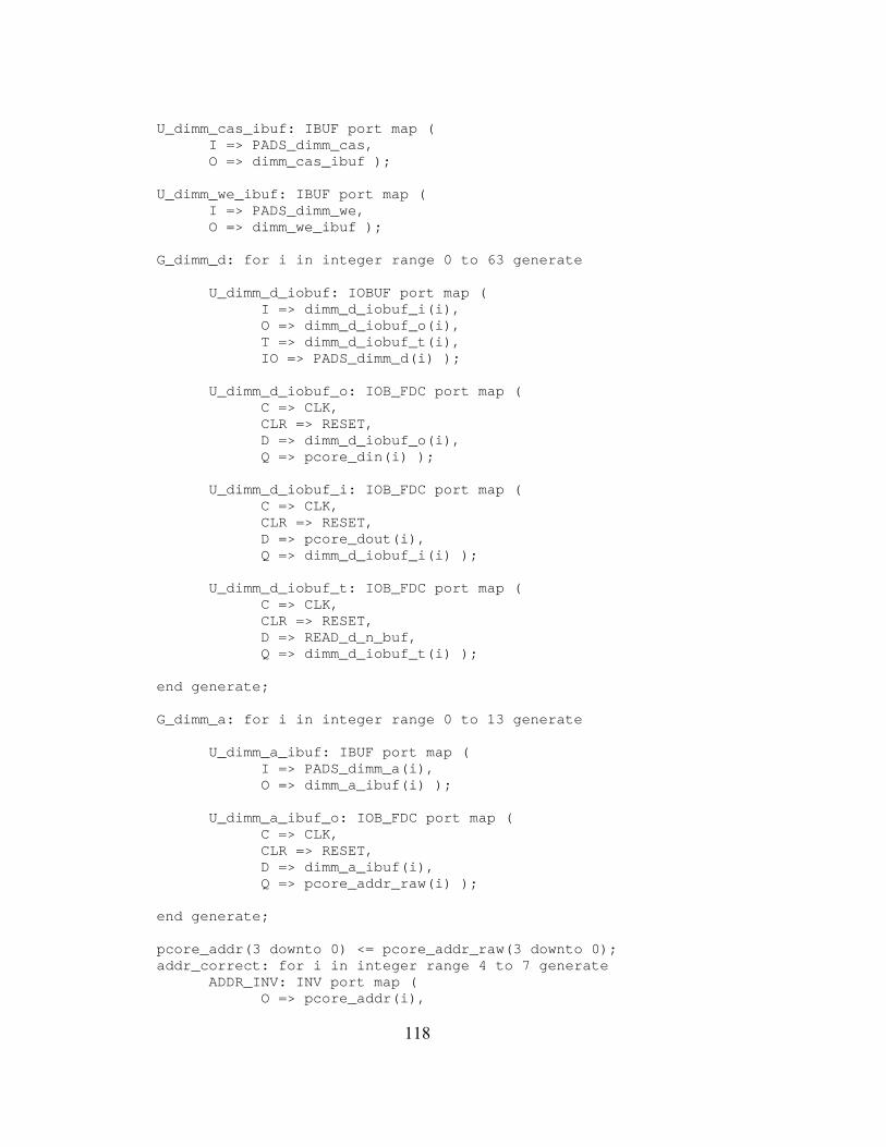
U_dimm_cas_ibuf: IBUF port map ( I => PADS_dimm_cas, O => dimm_cas_ibuf ); U_dimm_we_ibuf: IBUF port map ( I => PADS_dimm_we, O => dimm_we_ibuf ); G_dimm_d: for i in integer range 0 to 63 generate U_dimm_d_iobuf: IOBUF port map ( I => dimm_d_iobuf_i(i), O => dimm_d_iobuf_o(i), T => dimm_d_iobuf_t(i), IO => PADS_dimm_d(i) ); U_dimm_d_iobuf_o: IOB_FDC port map ( C => CLK, CLR => RESET, D => dimm_d_iobuf_o(i), Q => pcore_din(i) ); U_dimm_d_iobuf_i: IOB_FDC port map ( C => CLK, CLR => RESET, D => pcore_dout(i), Q => dimm_d_iobuf_i(i) ); U_dimm_d_iobuf_t: IOB_FDC port map ( C => CLK, CLR => RESET, D => READ_d_n_buf, Q => dimm_d_iobuf_t(i) ); end generate; G_dimm_a: for i in integer range 0 to 13 generate U_dimm_a_ibuf: IBUF port map ( I => PADS_dimm_a(i), O => dimm_a_ibuf(i) ); U_dimm_a_ibuf_o: IOB_FDC port map ( C => CLK, CLR => RESET, D => dimm_a_ibuf(i), Q => pcore_addr_raw(i) ); end generate; pcore_addr(3 downto 0) <= pcore_addr_raw(3 downto 0); addr_correct: for i in integer range 4 to 7 generate ADDR_INV: INV port map ( O => pcore_addr(i),
118
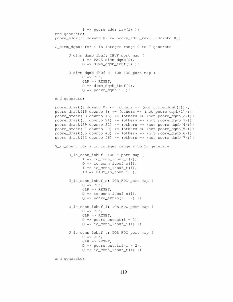
I => pcore_addr_raw(i) ); end generate; pcore_addr(13 downto 8) <= pcore_addr_raw(13 downto 8); G_dimm_dqmb: for i in integer range 0 to 7 generate U_dimm_dqmb_ibuf: IBUF port map ( I => PADS_dimm_dqmb(i), O => dimm_dqmb_ibuf(i) ); U_dimm_dqmb_ibuf_o: IOB_FDC port map ( C => CLK, CLR => RESET, D => dimm_dqmb_ibuf(i), Q => pcore_dqmb(i) ); end generate; pcore_dmask(7 downto 0) <= (others => (not pcore_dqmb(0))); pcore_dmask(15 downto 8) <= (others => (not pcore_dqmb(1))); pcore_dmask(23 downto 16) <= (others => (not pcore_dqmb(2))); pcore_dmask(31 downto 24) <= (others => (not pcore_dqmb(3))); pcore_dmask(39 downto 32) <= (others => (not pcore_dqmb(4))); pcore_dmask(47 downto 40) <= (others => (not pcore_dqmb(5))); pcore_dmask(55 downto 48) <= (others => (not pcore_dqmb(6))); pcore_dmask(63 downto 56) <= (others => (not pcore_dqmb(7))); G_io_conn: for i in integer range 2 to 27 generate U_io_conn_iobuf: IOBUF port map ( I => io_conn_iobuf_i(i), O => io_conn_iobuf_o(i), T => io_conn_iobuf_t(i), IO => PADS_io_conn(i) ); U_io_conn_iobuf_o: IOB_FDC port map ( C => CLK, CLR => RESET, D => io_conn_iobuf_o(i), Q => pcore_extin(i - 2) ); U_io_conn_iobuf_i: IOB_FDC port map ( C => CLK, CLR => RESET, D => pcore_extout(i - 2), Q => io_conn_iobuf_i(i) ); U_io_conn_iobuf_t: IOB_FDC port map ( C => CLK, CLR => RESET, D => pcore_extctrl(i - 2), Q => io_conn_iobuf_t(i) ); end generate;
119
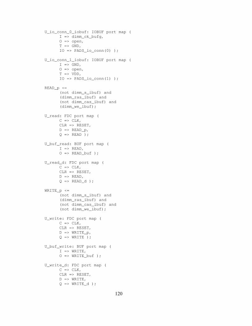
U_io_conn_0_iobuf: IOBUF port map ( I => dimm_ck_bufg, O => open, T => GND, IO => PADS_io_conn(0) ); U_io_conn_1_iobuf: IOBUF port map ( I => GND, O => open, T => VDD, IO => PADS_io_conn(1) ); READ_p <= (not dimm_s_ibuf) and (dimm_ras_ibuf) and (not dimm_cas_ibuf) and (dimm_we_ibuf); U_read: FDC port map ( C => CLK, CLR => RESET, D => READ_p, Q => READ ); U_buf_read: BUF port map ( I => READ, O => READ_buf ); U_read_d: FDC port map ( C => CLK, CLR => RESET, D => READ, Q => READ_d ); WRITE_p <= (not dimm_s_ibuf) and (dimm_ras_ibuf) and (not dimm_cas_ibuf) and (not dimm_we_ibuf); U_write: FDC port map ( C => CLK, CLR => RESET, D => WRITE_p, Q => WRITE ); U_buf_write: BUF port map ( I => WRITE, O => WRITE_buf ); U_write_d: FDC port map ( C => CLK, CLR => RESET, D => WRITE, Q => WRITE_d );
120
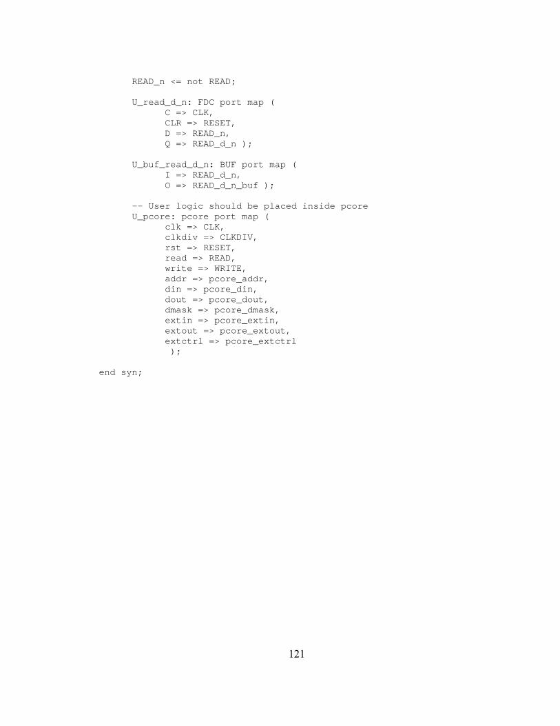
READ_n <= not READ; U_read_d_n: FDC port map ( C => CLK, CLR => RESET, D => READ_n, Q => READ_d_n ); U_buf_read_d_n: BUF port map ( I => READ_d_n, O => READ_d_n_buf ); -- User logic should be placed inside pcore U_pcore: pcore port map ( clk => CLK, clkdiv => CLKDIV, rst => RESET, read => READ, write => WRITE, addr => pcore_addr, din => pcore_din, dout => pcore_dout, dmask => pcore_dmask, extin => pcore_extin, extout => pcore_extout, extctrl => pcore_extctrl ); end syn;
121

Appendix E – Pcore.vhd
122
-- Pcore Wrapper -- Author: Kirk A Baugher library ieee; use ieee.std_logic_1164.all; use ieee.std_logic_unsigned.all; entity pcore is port ( clk: in std_logic; clkdiv: in std_logic; rst: in std_logic; read: in std_logic; write: in std_logic; addr: in std_logic_vector(13 downto 0); din: in std_logic_vector(63 downto 0); dout: out std_logic_vector(63 downto 0); dmask: in std_logic_vector(63 downto 0); extin: in std_logic_vector(25 downto 0); extout: out std_logic_vector(25 downto 0); extctrl: out std_logic_vector(25 downto 0) ); end pcore; architecture syn of pcore is component asyncfifo port ( din: IN std_logic_VECTOR(127 downto 0); wr_en: IN std_logic; wr_clk: IN std_logic; rd_en: IN std_logic; rd_clk: IN std_logic; ainit: IN std_logic; dout: OUT std_logic_VECTOR(127 downto 0); full: OUT std_logic; empty: OUT std_logic; rd_ack: OUT std_logic; rd_err: OUT std_logic; wr_ack: OUT std_logic; wr_err: OUT std_logic); END component; component sparsemvmult PORT( CLK :IN STD_LOGIC; RESET : IN STD_LOGIC; din_rdy : IN STD_LOGIC; INP : IN STD_LOGIC_VECTOR(127 DOWNTO 0); ADDR : OUT STD_LOGIC_VECTOR(1 DOWNTO 0); REPORTFLAG : OUT STD_LOGIC; ANS_FLAG_OUT : OUT STD_LOGIC; OUTPUT : OUT STD_LOGIC_VECTOR(63 DOWNTO 0)); END component; component outram
123
port ( addra: IN std_logic_VECTOR(1 downto 0); addrb: IN std_logic_VECTOR(1 downto 0); clka: IN std_logic; clkb: IN std_logic; dina: IN std_logic_VECTOR(63 downto 0); dinb: IN std_logic_VECTOR(63 downto 0); douta: OUT std_logic_VECTOR(63 downto 0); doutb: OUT std_logic_VECTOR(63 downto 0); wea: IN std_logic; web: IN std_logic); END component; signal wr_en, wr_ack, wr_err, rd_en, rd_ack, rd_err : std_logic; signal full, empty, din_rdy, tic,finish,ready,read2,read3,read4 : std_logic; signal FIFO_in, FIFO_out, out2parith :std_logic_vector(127 downto 0); signal parithout,temp :std_logic_vector(63 downto 0); signal wea,web,ndb,rfdb,rdyb,tac : std_logic; signal REPORTFLAG,ANS_FLAG_OUT : std_logic; signal dina,dinb,douta,doutb : std_logic_vector(63 downto 0); signal addrb : std_logic_vector(1 downto 0); begin fifo0: asyncfifo port map ( din =>FIFO_in, wr_en =>wr_en, wr_clk =>clk, rd_en =>rd_en, rd_clk =>clkdiv, ainit =>rst, dout =>FIFO_out, full =>full, empty =>empty, rd_ack =>rd_ack, rd_err =>rd_err, wr_ack =>wr_ack, wr_err =>wr_err ); smsv : sparsemvmult port map( CLK => clkdiv, RESET => rst, din_rdy => din_rdy, INP => out2parith, ADDR => addrb, REPORTFLAG => REPORTFLAG, ANS_FLAG_OUT => ANS_FLAG_OUT, OUTPUT => parithout ); outram0 : outram port map( addra => addr(1 downto 0),
124
addrb => addrb, clka => clk, clkb => clkdiv, dina => din, dinb => parithout, douta => douta, doutb => doutb, wea => write, web => finish ); finish <= (REPORTFLAG OR ANS_FLAG_OUT); process(clk,rst) variable tmpx : std_logic_vector(63 downto 0); begin if rst='1' then tmpx := (OTHERS=>'1'); wr_en <= '0'; tic <= '0'; FIFO_in <= (OTHERS=>'1'); elsif clk'event and clk='1' then if write='1' and addr(1)='0' then if tic = '0' then tmpx := din; tic <= '1'; wr_en <= '0'; else FIFO_in <= tmpx & din; wr_en <= '1'; tic <= '0'; end if; else wr_en <= '0'; tic <= tic; tmpx := tmpx; end if; end if; end process; process(clkdiv,rst) begin if rst='1' then rd_en <= '0'; elsif clkdiv'event and clkdiv='1' then if empty = '0' then rd_en <= '1'; else rd_en <= '0'; end if; end if; end process; process(clkdiv,rst) begin
125
if rst='1' then out2parith <= (OTHERS=>'1'); din_rdy <= '0'; elsif clkdiv'event and clkdiv='1' then if rd_err = '0' and rd_ack = '1' then out2parith <= FIFO_out; din_rdy <= '1'; else out2parith <= (OTHERS=>'1'); din_rdy <= '0'; end if; end if; end process; dout <= doutb; end syn;
126

Appendix F – Sparsemvmult.vhd
127

-- Sparse Matrix Sparse Vector Multiplier -- < sparsemvmult.vhd > -- 4/19/2004 -- Kirk A Baugher -- kbaugher.edu LIBRARY IEEE; USE IEEE.std_logic_1164.ALL; USE IEEE.std_logic_arith.ALL; use IEEE.std_logic_unsigned.all; ENTITY sparsemvmult IS PORT( CLK :IN STD_LOGIC; RESET : IN STD_LOGIC; din_rdy : IN STD_LOGIC; INP : IN STD_LOGIC_VECTOR(127 DOWNTO 0); ADDR : OUT STD_LOGIC_VECTOR(1 DOWNTO 0); REPORTFLAG : OUT STD_LOGIC; ANS_FLAG_OUT : OUT STD_LOGIC; OUTPUT : OUT STD_LOGIC_VECTOR(63 DOWNTO 0)); END sparsemvmult; ARCHITECTURE behavior OF sparsemvmult IS SIGNAL ANS_FLAG,overflag,New_vectorflag : STD_LOGIC; SIGNAL ANSWER : STD_LOGIC_VECTOR(63 DOWNTO 0); TYPE STATE_TYPE IS (ADDRESS, DATA, PROCESSING,INITIALIZE,REPORTw,REPORTx,SEND,MACN); SIGNAL STATE,STATEX,STATE_DEL : STATE_TYPE; TYPE elmnt_addr IS ARRAY (0 TO 31) OF STD_LOGIC_VECTOR(31 DOWNTO 0); SIGNAL ea : elmnt_addr; --TYPE elmnt_data IS ARRAY (0 TO 63) OF STD_LOGIC_VECTOR(63 DOWNTO 0); --SIGNAL ed : elmnt_data; SIGNAL j,gnd_bit : STD_LOGIC; SIGNAL i : INTEGER RANGE 0 TO 63; TYPE MACbuffer IS ARRAY (0 TO 63) OF STD_LOGIC_VECTOR(63 DOWNTO 0); SIGNAL buff,accbuff : MACbuffer; SIGNAL count1,count2 : INTEGER RANGE 0 TO 31; SIGNAL OUTPUT1,OUTPUT2,OUTPUT3,OUTPUT4: STD_LOGIC_VECTOR(13 DOWNTO 0); SIGNAL GND,rowcnt,rowcnt_less1,cntr : STD_LOGIC_VECTOR(31 DOWNTO 0); SIGNAL Acount,Acount1 : INTEGER RANGE 0 TO 13; SIGNAL Mult_in1A,Mult_in1B : STD_LOGIC_VECTOR(63 DOWNTO 0); SIGNAL Mult_in2A,Mult_in2B : STD_LOGIC_VECTOR(63 DOWNTO 0); SIGNAL over,stall,matchflag,one,din_rdy2 : STD_LOGIC; SIGNAL over11,over12,over13,over14,over1 : STD_LOGIC; SIGNAL match11,match12,match13,match14,match1,match1x : STD_LOGIC; SIGNAL OUTPUT11,OUTPUT12,OUTPUT13,OUTPUT14 : STD_LOGIC; --SIGNAL Dataout11,Dataout12,Dataout13,Dataout14,Dataout1 : STD_LOGIC_VECTOR(63 DOWNTO 0); SIGNAL over21,over22,over23,over24,over2 : STD_LOGIC; SIGNAL match21,match22,match23,match24,match2,match2x : STD_LOGIC; SIGNAL OUTPUT21,OUTPUT22,OUTPUT23,OUTPUT24 : STD_LOGIC; --SIGNAL Dataout21,Dataout22,Dataout23,Dataout24,Dataout2 : STD_LOGIC_VECTOR(63 DOWNTO 0); SIGNAL over31,over32,over33,over34,over3 : STD_LOGIC; SIGNAL match31,match32,match33,match34,match3,match3x : STD_LOGIC;
128
SIGNAL OUTPUT31,OUTPUT32,OUTPUT33,OUTPUT34 : STD_LOGIC; --SIGNAL Dataout31,Dataout32,Dataout33,Dataout34,Dataout3 : STD_LOGIC_VECTOR(63 DOWNTO 0); SIGNAL over41,over42,over43,over44,over4 : STD_LOGIC; SIGNAL match41,match42,match43,match44,match44x,match4,match4x : STD_LOGIC; SIGNAL OUTPUT41,OUTPUT42,OUTPUT43,OUTPUT44 : STD_LOGIC; --SIGNAL Dataout41,Dataout42,Dataout43,Dataout44,Dataout4 : STD_LOGIC_VECTOR(63 DOWNTO 0); SIGNAL spot : INTEGER RANGE 0 TO 55; SIGNAL addra1,addrb1,addra2,addrb2 : STD_LOGIC_VECTOR(5 DOWNTO 0); SIGNAL addra1x,addrb1x,addra2x,addrb2x : STD_LOGIC_VECTOR(5 DOWNTO 0); SIGNAL addra1z,addrb1z,addra2z,addrb2z : STD_LOGIC_VECTOR(5 DOWNTO 0); SIGNAL addra11,addrb11,addra21,addrb21 : STD_LOGIC_VECTOR(5 DOWNTO 0); SIGNAL addra12,addrb12,addra22,addrb22 : STD_LOGIC_VECTOR(5 DOWNTO 0); SIGNAL addra13,addrb13,addra23,addrb23 : STD_LOGIC_VECTOR(5 DOWNTO 0); SIGNAL addra14,addrb14,addra24,addrb24 : STD_LOGIC_VECTOR(5 DOWNTO 0); SIGNAL dina1,dinb1,dina2,dinb2 : STD_LOGIC_VECTOR(63 DOWNTO 0); SIGNAL douta1,doutb1,douta2,doutb2 : STD_LOGIC_VECTOR(63 DOWNTO 0); SIGNAL wea1,web1,wea2,web2 : STD_LOGIC; SIGNAL ia1,ia2,ia3,ia4 : STD_LOGIC_VECTOR(5 DOWNTO 0); ---------------------------------------------------------------------------------------- signal mout1,mout2,Aa,Xa,Ab,Xb,mout1a,mout2a : STD_LOGIC_VECTOR(63 DOWNTO 0); signal wr_enx : std_logic_vector(1 to 4); signal rd_en1,rd_ack1,rd_err1 : std_logic; signal wr_en1 : std_logic; signal rd_en2,rd_ack2,rd_err2 : std_logic; signal wr_en2 : std_logic; signal rd_en3,rd_ack3,rd_err3 : std_logic; signal wr_en3 : std_logic; signal rd_en4,rd_ack4,rd_err4 : std_logic; signal wr_en4 : std_logic; TYPE quadBufferin IS ARRAY (1 TO 4) OF std_logic_vector(63 downto 0); signal buffin : quadBufferin; signal dout1,dout2,dout3,dout4 : std_logic_vector(63 downto 0); signal empty1,empty2,empty3,empty4 : std_logic; signal full1,full2,full3,full4 : std_logic; signal sm1,sm2,fm1a,fm2a : std_logic; signal ptr1,ptr2,ptr3,ptr4 : integer range 1 to 4; signal sm1a,sm2a,sm1b,sm2b : std_logic; signal side1,side1a,side1b : std_logic;
129
signal side2,side2a,side2b : std_logic; ---------------------------------------------------------------------------------------- signal c,d,c1,c2,d1,Ain1,Ain2,aout : std_logic_vector(63 downto 0); signal rd_en,wr_enbuff : std_logic; signal sa,rd_err : std_logic; signal rd_ack : std_logic; signal ready : std_logic; signal fa,full_out : std_logic; signal empty_out : std_logic; signal dinbuff : std_logic_vector(63 downto 0); signal dout_out : std_logic_vector(63 downto 0); signal overflow_val,overflow_val2 : std_logic_vector(63 downto 0); signal overflow,overflow2 : std_logic; signal fm1,fm2,num_inputs : std_logic; signal instatus,inputstatus : integer range 0 to 9; signal size : integer range 0 to 64; signal pending : integer range 0 to 13; signal pendingm1,pendingm2 : integer range 0 to 9; signal buffreset : std_logic; ---------------------------------------------------------------------------------------- --signal rea1,rea2,rea3,rea4,rea5,rea6,rea7,rea8,rea9,reb1,reb2,reb3,reb4,reb5,reb6,reb7,reb8,reb9 : std_logic; ---------------------------------------------------------------------------------------- COMPONENT dpfpmult port ( CLK : in std_logic; A : in std_logic_vector(63 downto 0); B : in std_logic_vector(63 downto 0); OUTx : out std_logic_vector(63 downto 0); start: in std_logic; finish: out std_logic ); end COMPONENT; COMPONENT dpfpadd port ( CLK : in std_logic; Ain : in std_logic_vector(63 downto 0); Bin : in std_logic_vector(63 downto 0); OUTx : out std_logic_vector(63 downto 0); start: in std_logic; finish: out std_logic ); end COMPONENT; component syncfifo port ( clk: IN std_logic; sinit: IN std_logic; din: IN std_logic_VECTOR(63 downto 0);
130

wr_en: IN std_logic; rd_en: IN std_logic; dout: OUT std_logic_VECTOR(63 downto 0); full: OUT std_logic; empty: OUT std_logic; rd_ack: OUT std_logic; rd_err: OUT std_logic); end component; component dpram64_64 port ( addra: IN std_logic_VECTOR(5 downto 0); addrb: IN std_logic_VECTOR(5 downto 0); clka: IN std_logic; clkb: IN std_logic; dina: IN std_logic_VECTOR(63 downto 0); dinb: IN std_logic_VECTOR(63 downto 0); douta: OUT std_logic_VECTOR(63 downto 0); doutb: OUT std_logic_VECTOR(63 downto 0); wea: IN std_logic; web: IN std_logic); END component; BEGIN GND<=(OTHERS=>'0'); gnd_bit<='0'; one <= '1'; ram1 : dpram64_64 port map( addra => addra1, addrb => addrb1, clka => clk, clkb => clk, dina => dina1, dinb => dinb1, douta => douta1, doutb => doutb1, wea => wea1, web => web1 ); ram2 : dpram64_64 port map( addra => addra2, addrb => addrb2, clka => clk, clkb => clk, dina => dina2, dinb => dinb2, douta => douta2, doutb => doutb2, wea => wea2, web => web2 ); fpmult1 : dpfpmult port map(
131
CLK=>CLK, A=>Mult_in1A, B=>Mult_in1B, OUTx=>mout1, start=>sm1, finish=>fm1 ); fpmult2 : dpfpmult port map( CLK=>CLK, A=>Mult_in2A, B=>Mult_in2B, OUTx=>mout2, start=>sm2, finish=>fm2 ); fpadd : dpfpadd port map( CLK=>CLK, Ain=>Ain1, Bin=>Ain2, OUTx=>aout, start=>sa, finish=>fa); buf:syncfifo port map ( clk => clk, din => dinbuff, wr_en => wr_enbuff, rd_en => rd_en, sinit => buffreset, dout => dout_out, full => full_out, empty => empty_out, rd_ack => rd_ack, rd_err => rd_err ); buf1:syncfifo port map ( clk => clk, din => buffin(1), wr_en => wr_enx(1), rd_en => rd_en1, sinit => buffreset, dout => dout1, full => full1, empty => empty1, rd_ack => rd_ack1, rd_err => rd_err1 ); buf2:syncfifo port map ( clk => clk, din => buffin(2), wr_en => wr_enx(2), rd_en => rd_en2, sinit => buffreset,
132
dout => dout2, full => full2, empty => empty2, rd_ack => rd_ack2, rd_err => rd_err2 ); buf3:syncfifo port map ( clk => clk, din => buffin(3), wr_en => wr_enx(3), rd_en => rd_en3, sinit => buffreset, dout => dout3, full => full3, empty => empty3, rd_ack => rd_ack3, rd_err => rd_err3 ); buf4:syncfifo port map ( clk => clk, din => buffin(4), wr_en => wr_enx(4), rd_en => rd_en4, sinit => buffreset, dout => dout4, full => full4, empty => empty4, rd_ack => rd_ack4, rd_err => rd_err4 ); --buffreset <= reset OR ANS_FLAG; --mout1 <= mout1a when rea9='0' else (OTHERS=>'0'); --mout2 <= mout2a when reb9='0' else (OTHERS=>'0'); --fm1 <= fm1a when rea9='0' else '0'; --fm2 <= fm2a when reb9='0' else '0'; MAIN: PROCESS (CLK,RESET) VARIABLE w : INTEGER RANGE 0 TO 3; VARIABLE over,reportflagx : std_logic; BEGIN IF RESET='1' THEN STATE<=INITIALIZE; STATEX<=INITIALIZE; ANS_FLAG_OUT <= '0'; w:=0; i<=0; j<='0'; Acount<=13; --overflag <= '0'; over := '0'; reportflagx := '0'; ADDR <= "10"; --match := '0'; OUTPUT<=(OTHERS=>'0');
133
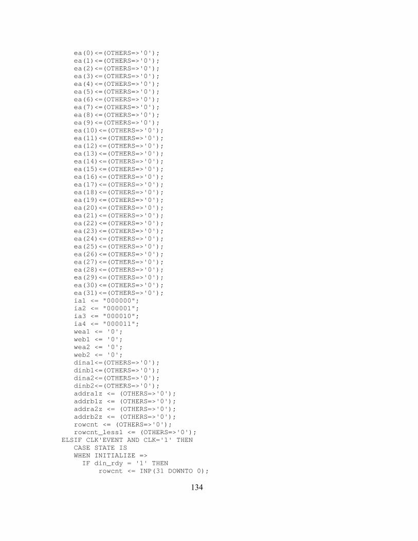
ea(0)<=(OTHERS=>'0'); ea(1)<=(OTHERS=>'0'); ea(2)<=(OTHERS=>'0'); ea(3)<=(OTHERS=>'0'); ea(4)<=(OTHERS=>'0'); ea(5)<=(OTHERS=>'0'); ea(6)<=(OTHERS=>'0'); ea(7)<=(OTHERS=>'0'); ea(8)<=(OTHERS=>'0'); ea(9)<=(OTHERS=>'0'); ea(10)<=(OTHERS=>'0'); ea(11)<=(OTHERS=>'0'); ea(12)<=(OTHERS=>'0'); ea(13)<=(OTHERS=>'0'); ea(14)<=(OTHERS=>'0'); ea(15)<=(OTHERS=>'0'); ea(16)<=(OTHERS=>'0'); ea(17)<=(OTHERS=>'0'); ea(18)<=(OTHERS=>'0'); ea(19)<=(OTHERS=>'0'); ea(20)<=(OTHERS=>'0'); ea(21)<=(OTHERS=>'0'); ea(22)<=(OTHERS=>'0'); ea(23)<=(OTHERS=>'0'); ea(24)<=(OTHERS=>'0'); ea(25)<=(OTHERS=>'0'); ea(26)<=(OTHERS=>'0'); ea(27)<=(OTHERS=>'0'); ea(28)<=(OTHERS=>'0'); ea(29)<=(OTHERS=>'0'); ea(30)<=(OTHERS=>'0'); ea(31)<=(OTHERS=>'0'); ia1 <= "000000"; ia2 <= "000001"; ia3 <= "000010"; ia4 <= "000011"; wea1 <= '0'; web1 <= '0'; wea2 <= '0'; web2 <= '0'; dina1<=(OTHERS=>'0'); dinb1<=(OTHERS=>'0'); dina2<=(OTHERS=>'0'); dinb2<=(OTHERS=>'0'); addra1z <= (OTHERS=>'0'); addrb1z <= (OTHERS=>'0'); addra2z <= (OTHERS=>'0'); addrb2z <= (OTHERS=>'0'); rowcnt <= (OTHERS=>'0'); rowcnt_less1 <= (OTHERS=>'0'); ELSIF CLK'EVENT AND CLK='1' THEN CASE STATE IS WHEN INITIALIZE => IF din_rdy = '1' THEN rowcnt <= INP(31 DOWNTO 0);
134
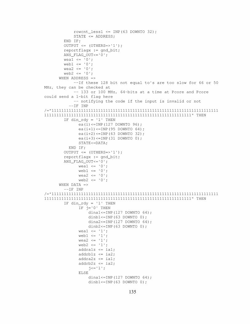
rowcnt_less1 <= INP(63 DOWNTO 32); STATE <= ADDRESS; END IF; OUTPUT <= (OTHERS=>'1'); reportflagx := gnd_bit; ANS_FLAG_OUT<='0'; wea1 <= '0'; web1 <= '0'; wea2 <= '0'; web2 <= '0'; WHEN ADDRESS => --If these 128 bit not equal to's are too slow for 66 or 50 MHz, they can be checked at -- 133 or 100 MHz, 64-bits at a time at Pcore and Pcore could send a 1-bit flag here -- notifying the code if the input is invalid or not --IF INP /="11111111111111111111111111111111111111111111111111111111111111111111111111111111111111111111111111111111111111111111111111111111" THEN IF din_rdy = '1' THEN ea(i)<=INP(127 DOWNTO 96); ea(i+1)<=INP(95 DOWNTO 64); ea(i+2)<=INP(63 DOWNTO 32); ea(i+3)<=INP(31 DOWNTO 0); STATE<=DATA; END IF; OUTPUT <= (OTHERS=>'1'); reportflagx := gnd_bit; ANS_FLAG_OUT<='0'; wea1 <= '0'; web1 <= '0'; wea2 <= '0'; web2 <= '0'; WHEN DATA => --IF INP /="11111111111111111111111111111111111111111111111111111111111111111111111111111111111111111111111111111111111111111111111111111111" THEN IF din_rdy = '1' THEN IF j='0' THEN dina1<=INP(127 DOWNTO 64); dinb1<=INP(63 DOWNTO 0); dina2<=INP(127 DOWNTO 64); dinb2<=INP(63 DOWNTO 0); wea1 <= '1'; web1 <= '1'; wea2 <= '1'; web2 <= '1'; addra1z <= ia1; addrb1z <= ia2; addra2z <= ia1; addrb2z <= ia2; j<='1'; ELSE dina1<=INP(127 DOWNTO 64); dinb1<=INP(63 DOWNTO 0);
135

dina2<=INP(127 DOWNTO 64); dinb2<=INP(63 DOWNTO 0); wea1 <= '1'; web1 <= '1'; wea2 <= '1'; web2 <= '1'; addra1z <= ia3; addrb1z <= ia4; addra2z <= ia3; addrb2z <= ia4; j<='0'; IF i<28 THEN STATE<=ADDRESS; i<=i+4; ia1 <= ia1 + "000100"; ia2 <= ia2 + "000100"; ia3 <= ia3 + "000100"; ia4 <= ia4 + "000100"; ELSE STATE<=PROCESSING; i<=0; ia1 <= "000000"; ia2 <= "000001"; ia3 <= "000010"; ia4 <= "000011"; END IF; END IF; END IF; OUTPUT <= (OTHERS=>'1'); reportflagx := gnd_bit; WHEN PROCESSING => --Don't decrement the counter if the input is invalid!! --Reading in addresses for comparators here wea1 <= '0'; web1 <= '0'; wea2 <= '0'; web2 <= '0'; IF din_rdy='1' THEN ADDR <= "10"; IF Acount = 0 THEN Acount<=13; STATE<=REPORTw; ELSE Acount<=Acount-1; -- OUTPUT<=(OTHERS=>'0'); END IF; OUTPUT <= (OTHERS=>'1'); END IF; ANS_FLAG_OUT<='0'; reportflagx := gnd_bit; WHEN REPORTw => STATE <= REPORTx; reportflagx := gnd_bit; WHEN REPORTx => reportflagx := one;
136
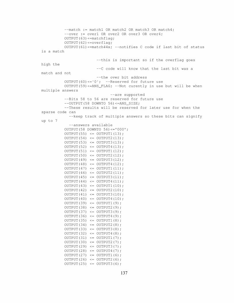
--match := match1 OR match2 OR match3 OR match4; --over := over1 OR over2 OR over3 OR over4; OUTPUT(63)<=matchflag; OUTPUT(62)<=overflag; OUTPUT(61)<=match44x; --notifies C code if last bit of status is a match --this is important so if the overflag goes high the --C code will know that the last bit was a match and not --the over bit address OUTPUT(60)<='0'; --Reserved for future use OUTPUT(59)<=ANS_FLAG; --Not curently in use but will be when multiple answers --are supported --Bits 58 to 56 are reserved for future use --OUTPUT(58 DOWNTO 56)<=ANS_SIZE; --These results will be reserved for later use for when the sparse code can --keep track of multiple answers so these bits can signify up to 7 --answers available OUTPUT(58 DOWNTO 56)<="000"; OUTPUT(55) <= OUTPUT1(13); OUTPUT(54) <= OUTPUT2(13); OUTPUT(53) <= OUTPUT3(13); OUTPUT(52) <= OUTPUT4(13); OUTPUT(51) <= OUTPUT1(12); OUTPUT(50) <= OUTPUT2(12); OUTPUT(49) <= OUTPUT3(12); OUTPUT(48) <= OUTPUT4(12); OUTPUT(47) <= OUTPUT1(11); OUTPUT(46) <= OUTPUT2(11); OUTPUT(45) <= OUTPUT3(11); OUTPUT(44) <= OUTPUT4(11); OUTPUT(43) <= OUTPUT1(10); OUTPUT(42) <= OUTPUT2(10); OUTPUT(41) <= OUTPUT3(10); OUTPUT(40) <= OUTPUT4(10); OUTPUT(39) <= OUTPUT1(9); OUTPUT(38) <= OUTPUT2(9); OUTPUT(37) <= OUTPUT3(9); OUTPUT(36) <= OUTPUT4(9); OUTPUT(35) <= OUTPUT1(8); OUTPUT(34) <= OUTPUT2(8); OUTPUT(33) <= OUTPUT3(8); OUTPUT(32) <= OUTPUT4(8); OUTPUT(31) <= OUTPUT1(7); OUTPUT(30) <= OUTPUT2(7); OUTPUT(29) <= OUTPUT3(7); OUTPUT(28) <= OUTPUT4(7); OUTPUT(27) <= OUTPUT1(6); OUTPUT(26) <= OUTPUT2(6); OUTPUT(25) <= OUTPUT3(6);
137
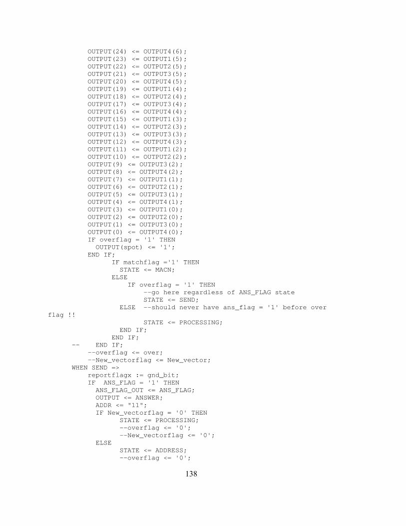
OUTPUT(24) <= OUTPUT4(6); OUTPUT(23) <= OUTPUT1(5); OUTPUT(22) <= OUTPUT2(5); OUTPUT(21) <= OUTPUT3(5); OUTPUT(20) <= OUTPUT4(5); OUTPUT(19) <= OUTPUT1(4); OUTPUT(18) <= OUTPUT2(4); OUTPUT(17) <= OUTPUT3(4); OUTPUT(16) <= OUTPUT4(4); OUTPUT(15) <= OUTPUT1(3); OUTPUT(14) <= OUTPUT2(3); OUTPUT(13) <= OUTPUT3(3); OUTPUT(12) <= OUTPUT4(3); OUTPUT(11) <= OUTPUT1(2); OUTPUT(10) <= OUTPUT2(2); OUTPUT(9) <= OUTPUT3(2); OUTPUT(8) <= OUTPUT4(2); OUTPUT(7) <= OUTPUT1(1); OUTPUT(6) <= OUTPUT2(1); OUTPUT(5) <= OUTPUT3(1); OUTPUT(4) <= OUTPUT4(1); OUTPUT(3) <= OUTPUT1(0); OUTPUT(2) <= OUTPUT2(0); OUTPUT(1) <= OUTPUT3(0); OUTPUT(0) <= OUTPUT4(0); IF overflag = '1' THEN OUTPUT(spot) <= '1'; END IF; IF matchflag ='1' THEN STATE <= MACN; ELSE IF overflag = '1' THEN --go here regardless of ANS_FLAG state STATE <= SEND; ELSE --should never have ans_flag = '1' before over flag !! STATE <= PROCESSING; END IF; END IF; -- END IF; --overflag <= over; --New_vectorflag <= New_vector; WHEN SEND => reportflagx := gnd_bit; IF ANS_FLAG = '1' THEN ANS_FLAG_OUT <= ANS_FLAG; OUTPUT <= ANSWER; ADDR <= "11"; IF New_vectorflag = '0' THEN STATE <= PROCESSING; --overflag <= '0'; --New_vectorflag <= '0'; ELSE STATE <= ADDRESS; --overflag <= '0';
138
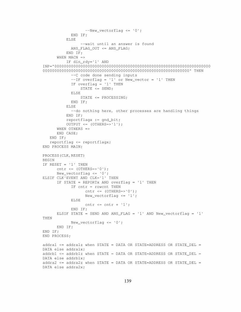
--New_vectorflag <= '0'; END IF; ELSE --wait until an answer is found ANS_FLAG_OUT <= ANS_FLAG; END IF; WHEN MACN => IF din_rdy='1' AND INP="00000000000000000000000000000000000000000000000000000000000000000000000000000000000000000000000000000000000000000000000000000000" THEN --C code done sending inputs --IF overflag = '1' or New_vector = '1' THEN IF overflag = '1' THEN STATE <= SEND; ELSE STATE <= PROCESSING; END IF; ELSE --do nothing here, other processes are handling things END IF; reportflagx := gnd_bit; OUTPUT <= (OTHERS=>'1'); WHEN OTHERS => END CASE; END IF; reportflag <= reportflagx; END PROCESS MAIN; PROCESS(CLK,RESET) BEGIN IF RESET = '1' THEN cntr <= (OTHERS=>'0'); New_vectorflag <= '0'; ELSIF CLK'EVENT AND CLK='1' THEN IF STATE = REPORTx AND overflag = '1' THEN IF cntr = rowcnt THEN cntr <= (OTHERS=>'0'); New_vectorflag <= '1'; ELSE cntr <= cntr + '1'; END IF; ELSIF STATE = SEND AND ANS_FLAG = '1' AND New_vectorflag = '1' THEN New_vectorflag <= '0'; END IF; END IF; END PROCESS; addra1 <= addra1z when STATE = DATA OR STATE=ADDRESS OR STATE_DEL = DATA else addra1x; addrb1 <= addrb1z when STATE = DATA OR STATE=ADDRESS OR STATE_DEL = DATA else addrb1x; addra2 <= addra2z when STATE = DATA OR STATE=ADDRESS OR STATE_DEL = DATA else addra2x;
139
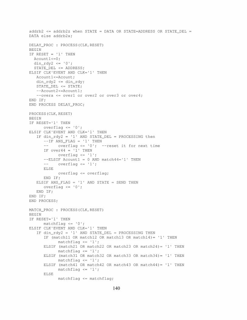
addrb2 <= addrb2z when STATE = DATA OR STATE=ADDRESS OR STATE_DEL = DATA else addrb2x; DELAY_PROC : PROCESS(CLK,RESET) BEGIN IF RESET = '1' THEN Acount1<=0; din_rdy2 <= '0'; STATE_DEL <= ADDRESS; ELSIF CLK'EVENT AND CLK='1' THEN Acount1<=Acount; din_rdy2 <= din_rdy; STATE_DEL <= STATE; --Acount2<=Acount1; --overa <= over1 or over2 or over3 or over4; END IF; END PROCESS DELAY_PROC; PROCESS(CLK,RESET) BEGIN IF RESET='1' THEN overflag <= '0'; ELSIF CLK'EVENT AND CLK='1' THEN IF din_rdy2 = '1' AND STATE_DEL = PROCESSING then --IF ANS_FLAG = '1' THEN -- overflag <= '0'; --reset it for next time IF over44 = '1' THEN overflag <= '1'; --ELSIF Acount1 = 0 AND match44='1' THEN -- overflag <= '1'; ELSE overflag <= overflag; END IF; ELSIF ANS_FLAG = '1' AND STATE = SEND THEN overflag <= '0'; END IF; END IF; END PROCESS; MATCH_PROC : PROCESS(CLK,RESET) BEGIN IF RESET='1' THEN matchflag <= '0'; ELSIF CLK'EVENT AND CLK='1' THEN IF din_rdy2 = '1' AND STATE_DEL = PROCESSING THEN IF (match11 OR match12 OR match13 OR match14)= '1' THEN matchflag <= '1'; ELSIF (match21 OR match22 OR match23 OR match24)= '1' THEN matchflag <= '1'; ELSIF (match31 OR match32 OR match33 OR match34)= '1' THEN matchflag <= '1'; ELSIF (match41 OR match42 OR match43 OR match44)= '1' THEN matchflag <= '1'; ELSE matchflag <= matchflag;
140
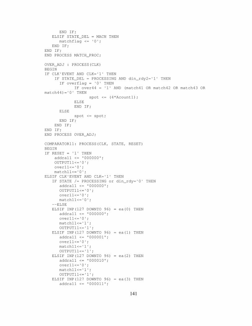
END IF; ELSIF STATE_DEL = MACN THEN matchflag <= '0'; END IF; END IF; END PROCESS MATCH_PROC; OVER_ADJ : PROCESS(CLK) BEGIN IF CLK'EVENT AND CLK='1' THEN IF STATE_DEL = PROCESSING AND din_rdy2='1' THEN IF overflag = '0' THEN IF over44 = '1' AND (match41 OR match42 OR match43 OR match44)='0' THEN spot <= (4*Acount1); ELSE END IF; ELSE spot <= spot; END IF; END IF; END IF; END PROCESS OVER_ADJ; COMPARATOR11: PROCESS(CLK, STATE, RESET) BEGIN IF RESET = '1' THEN addra11 <= "000000"; OUTPUT11<='0'; over11<='0'; match11<='0'; ELSIF CLK'EVENT AND CLK='1' THEN IF STATE /= PROCESSING or din_rdy='0' THEN addra11 <= "000000"; OUTPUT11<='0'; over11<='0'; match11<='0'; --ELSE ELSIF INP(127 DOWNTO 96) = ea(0) THEN addra11 <= "000000"; over11<='0'; match11<='1'; OUTPUT11<='1'; ELSIF INP(127 DOWNTO 96) = ea(1) THEN addra11 <= "000001"; over11<='0'; match11<='1'; OUTPUT11<='1'; ELSIF INP(127 DOWNTO 96) = ea(2) THEN addra11 <= "000010"; over11<='0'; match11<='1'; OUTPUT11<='1'; ELSIF INP(127 DOWNTO 96) = ea(3) THEN addra11 <= "000011";
141
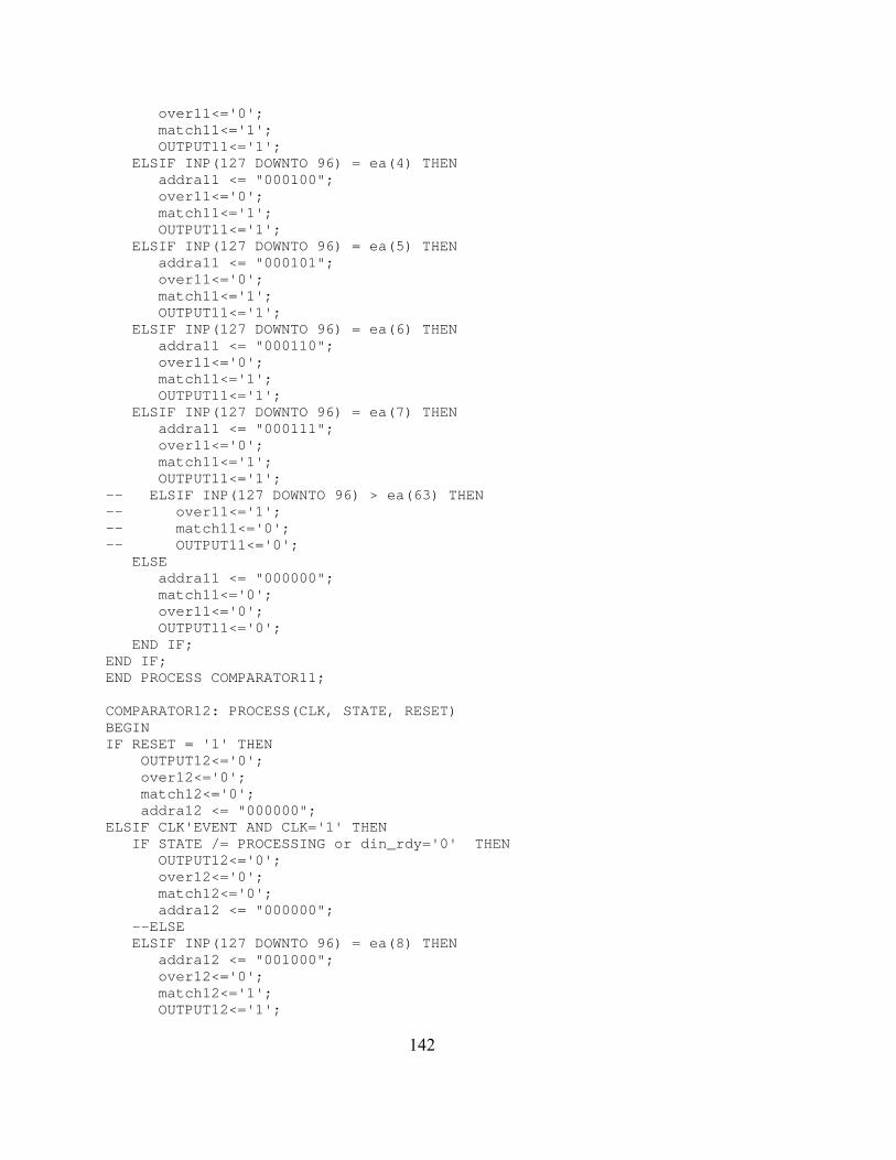
over11<='0'; match11<='1'; OUTPUT11<='1'; ELSIF INP(127 DOWNTO 96) = ea(4) THEN addra11 <= "000100"; over11<='0'; match11<='1'; OUTPUT11<='1'; ELSIF INP(127 DOWNTO 96) = ea(5) THEN addra11 <= "000101"; over11<='0'; match11<='1'; OUTPUT11<='1'; ELSIF INP(127 DOWNTO 96) = ea(6) THEN addra11 <= "000110"; over11<='0'; match11<='1'; OUTPUT11<='1'; ELSIF INP(127 DOWNTO 96) = ea(7) THEN addra11 <= "000111"; over11<='0'; match11<='1'; OUTPUT11<='1'; -- ELSIF INP(127 DOWNTO 96) > ea(63) THEN -- over11<='1'; -- match11<='0'; -- OUTPUT11<='0'; ELSE addra11 <= "000000"; match11<='0'; over11<='0'; OUTPUT11<='0'; END IF; END IF; END PROCESS COMPARATOR11; COMPARATOR12: PROCESS(CLK, STATE, RESET) BEGIN IF RESET = '1' THEN OUTPUT12<='0'; over12<='0'; match12<='0'; addra12 <= "000000"; ELSIF CLK'EVENT AND CLK='1' THEN IF STATE /= PROCESSING or din_rdy='0' THEN OUTPUT12<='0'; over12<='0'; match12<='0'; addra12 <= "000000"; --ELSE ELSIF INP(127 DOWNTO 96) = ea(8) THEN addra12 <= "001000"; over12<='0'; match12<='1'; OUTPUT12<='1';
142
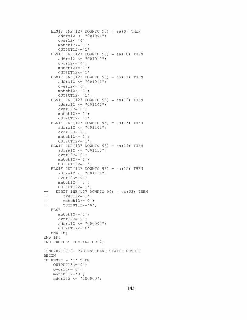
ELSIF INP(127 DOWNTO 96) = ea(9) THEN addra12 <= "001001"; over12<='0'; match12<='1'; OUTPUT12<='1'; ELSIF INP(127 DOWNTO 96) = ea(10) THEN addra12 <= "001010"; over12<='0'; match12<='1'; OUTPUT12<='1'; ELSIF INP(127 DOWNTO 96) = ea(11) THEN addra12 <= "001011"; over12<='0'; match12<='1'; OUTPUT12<='1'; ELSIF INP(127 DOWNTO 96) = ea(12) THEN addra12 <= "001100"; over12<='0'; match12<='1'; OUTPUT12<='1'; ELSIF INP(127 DOWNTO 96) = ea(13) THEN addra12 <= "001101"; over12<='0'; match12<='1'; OUTPUT12<='1'; ELSIF INP(127 DOWNTO 96) = ea(14) THEN addra12 <= "001110"; over12<='0'; match12<='1'; OUTPUT12<='1'; ELSIF INP(127 DOWNTO 96) = ea(15) THEN addra12 <= "001111"; over12<='0'; match12<='1'; OUTPUT12<='1'; -- ELSIF INP(127 DOWNTO 96) > ea(63) THEN -- over12<='1'; -- match12<='0'; -- OUTPUT12<='0'; ELSE match12<='0'; over12<='0'; addra12 <= "000000"; OUTPUT12<='0'; END IF; END IF; END PROCESS COMPARATOR12; COMPARATOR13: PROCESS(CLK, STATE, RESET) BEGIN IF RESET = '1' THEN OUTPUT13<='0'; over13<='0'; match13<='0'; addra13 <= "000000";
143
ELSIF CLK'EVENT AND CLK='1' THEN IF STATE /= PROCESSING or din_rdy='0' THEN OUTPUT13<='0'; over13<='0'; match13<='0'; addra13 <= "000000"; --ELSE ELSIF INP(127 DOWNTO 96) = ea(16) THEN over13<='0'; match13<='1'; OUTPUT13<='1'; addra13 <= "010000"; ELSIF INP(127 DOWNTO 96) = ea(17) THEN over13<='0'; match13<='1'; OUTPUT13<='1'; addra13 <= "010001"; ELSIF INP(127 DOWNTO 96) = ea(18) THEN over13<='0'; match13<='1'; OUTPUT13<='1'; addra13 <= "010010"; ELSIF INP(127 DOWNTO 96) = ea(19) THEN over13<='0'; match13<='1'; OUTPUT13<='1'; addra13 <= "010011"; ELSIF INP(127 DOWNTO 96) = ea(20) THEN over13<='0'; match13<='1'; OUTPUT13<='1'; addra13 <= "010100"; ELSIF INP(127 DOWNTO 96) = ea(21) THEN over13<='0'; match13<='1'; OUTPUT13<='1'; addra13 <= "010101"; ELSIF INP(127 DOWNTO 96) = ea(22) THEN over13<='0'; match13<='1'; OUTPUT13<='1'; addra13 <= "010110"; ELSIF INP(127 DOWNTO 96) = ea(23) THEN over13<='0'; match13<='1'; OUTPUT13<='1'; addra13 <= "010111"; -- ELSIF INP(127 DOWNTO 96) > ea(63) THEN -- over13<='1'; -- match13<='0'; -- OUTPUT13<='0'; ELSE match13<='0'; over13<='0'; addra13 <= "000000";
144
OUTPUT13<='0'; END IF; END IF; END PROCESS COMPARATOR13; COMPARATOR14: PROCESS(CLK, STATE, RESET) BEGIN IF RESET = '1' THEN addra14 <= "000000"; OUTPUT14<='0'; over14<='0'; match14<='0'; ELSIF CLK'EVENT AND CLK='1' THEN IF STATE /= PROCESSING or din_rdy='0' THEN OUTPUT14<='0'; over14<='0'; match14<='0'; addra14 <= "000000"; --ELSE ELSIF INP(127 DOWNTO 96) = ea(24) THEN over14<='0'; match14<='1'; OUTPUT14<='1'; addra14 <= "011000"; ELSIF INP(127 DOWNTO 96) = ea(25) THEN over14<='0'; match14<='1'; OUTPUT14<='1'; addra14 <= "011001"; ELSIF INP(127 DOWNTO 96) = ea(26) THEN over14<='0'; match14<='1'; OUTPUT14<='1'; addra14 <= "011010"; ELSIF INP(127 DOWNTO 96) = ea(27) THEN over14<='0'; match14<='1'; OUTPUT14<='1'; addra14 <= "011011"; ELSIF INP(127 DOWNTO 96) = ea(28) THEN over14<='0'; match14<='1'; OUTPUT14<='1'; addra14 <= "011100"; ELSIF INP(127 DOWNTO 96) = ea(29) THEN over14<='0'; match14<='1'; OUTPUT14<='1'; addra14 <= "011101"; ELSIF INP(127 DOWNTO 96) = ea(30) THEN over14<='0'; match14<='1'; OUTPUT14<='1'; addra14 <= "011110"; ELSIF INP(127 DOWNTO 96) = ea(31) THEN
145

over14<='0'; match14<='1'; OUTPUT14<='1'; addra14 <= "011111"; ELSIF INP(127 DOWNTO 96) > ea(31) THEN --over14<='1'; match14<='0'; OUTPUT14<='0'; ELSE match14<='0'; over14<='0'; addra14 <= "000000"; OUTPUT14<='0'; END IF; END IF; END PROCESS COMPARATOR14; MUXER1: PROCESS(CLK, RESET) variable match1a : std_logic; BEGIN IF RESET='1' THEN --over1 <= '0'; match1x <= '0'; addra1x <= (OTHERS=>'0'); OUTPUT1 <= (OTHERS=>'0'); match1a := '0'; ELSIF CLK'EVENT AND CLK='1' THEN --over1<=over11 OR over12 OR over13 OR over14; match1a:=match11 OR match12 OR match13 OR match14; match1x<=match1a; OUTPUT1(Acount1) <= OUTPUT11 OR OUTPUT12 OR OUTPUT13 OR OUTPUT14; IF match11 = '1' THEN addra1x <= addra11; ELSIF match12 = '1' THEN addra1x <= addra12; ELSIF match13 = '1' THEN addra1x <= addra13; ELSIF match14 = '1' THEN addra1x <= addra14; ELSE addra1x <= (OTHERS=>'0'); END IF; END IF; END PROCESS MUXER1; COMPARATOR21: PROCESS(CLK, STATE, RESET) BEGIN IF RESET = '1' THEN OUTPUT21<='0'; over21<='0'; match21<='0'; addrb11 <= "000000"; ELSIF CLK'EVENT AND CLK='1' THEN IF STATE /= PROCESSING or din_rdy='0' THEN OUTPUT21<='0';
146
over21<='0'; match21<='0'; addrb11 <= "000000"; --ELSE ELSIF INP(95 DOWNTO 64) = ea(0) THEN over21<='0'; match21<='1'; OUTPUT21<='1'; addrb11 <= "000000"; ELSIF INP(95 DOWNTO 64) = ea(1) THEN over21<='0'; match21<='1'; OUTPUT21<='1'; addrb11 <= "000001"; ELSIF INP(95 DOWNTO 64) = ea(2) THEN over21<='0'; match21<='1'; OUTPUT21<='1'; addrb11 <= "000010"; ELSIF INP(95 DOWNTO 64) = ea(3) THEN over21<='0'; match21<='1'; OUTPUT21<='1'; addrb11 <= "000011"; ELSIF INP(95 DOWNTO 64) = ea(4) THEN over21<='0'; match21<='1'; OUTPUT21<='1'; addrb11 <= "000100"; ELSIF INP(95 DOWNTO 64) = ea(5) THEN over21<='0'; match21<='1'; OUTPUT21<='1'; addrb11 <= "000101"; ELSIF INP(95 DOWNTO 64) = ea(6) THEN over21<='0'; match21<='1'; OUTPUT21<='1'; addrb11 <= "000110"; ELSIF INP(95 DOWNTO 64) = ea(7) THEN over21<='0'; match21<='1'; OUTPUT21<='1'; addrb11 <= "000111"; -- ELSIF INP(95 DOWNTO 64) > ea(63) THEN -- over21<='1'; -- match21<='0'; -- OUTPUT21<='0'; ELSE match21<='0'; over21<='0'; addrb11 <= "000000"; OUTPUT21<='0'; END IF; END IF;
147
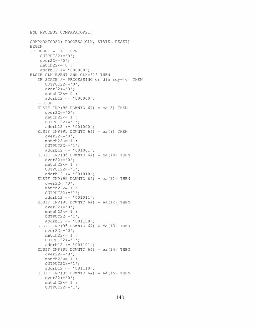
END PROCESS COMPARATOR21; COMPARATOR22: PROCESS(CLK, STATE, RESET) BEGIN IF RESET = '1' THEN OUTPUT22<='0'; over22<='0'; match22<='0'; addrb12 <= "000000"; ELSIF CLK'EVENT AND CLK='1' THEN IF STATE /= PROCESSING or din_rdy='0' THEN OUTPUT22<='0'; over22<='0'; match22<='0'; addrb12 <= "000000"; --ELSE ELSIF INP(95 DOWNTO 64) = ea(8) THEN over22<='0'; match22<='1'; OUTPUT22<='1'; addrb12 <= "001000"; ELSIF INP(95 DOWNTO 64) = ea(9) THEN over22<='0'; match22<='1'; OUTPUT22<='1'; addrb12 <= "001001"; ELSIF INP(95 DOWNTO 64) = ea(10) THEN over22<='0'; match22<='1'; OUTPUT22<='1'; addrb12 <= "001010"; ELSIF INP(95 DOWNTO 64) = ea(11) THEN over22<='0'; match22<='1'; OUTPUT22<='1'; addrb12 <= "001011"; ELSIF INP(95 DOWNTO 64) = ea(12) THEN over22<='0'; match22<='1'; OUTPUT22<='1'; addrb12 <= "001100"; ELSIF INP(95 DOWNTO 64) = ea(13) THEN over22<='0'; match22<='1'; OUTPUT22<='1'; addrb12 <= "001101"; ELSIF INP(95 DOWNTO 64) = ea(14) THEN over22<='0'; match22<='1'; OUTPUT22<='1'; addrb12 <= "001110"; ELSIF INP(95 DOWNTO 64) = ea(15) THEN over22<='0'; match22<='1'; OUTPUT22<='1';
148
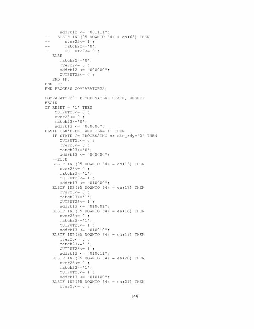
addrb12 <= "001111"; -- ELSIF INP(95 DOWNTO 64) > ea(63) THEN -- over22<='1'; -- match22<='0'; -- OUTPUT22<='0'; ELSE match22<='0'; over22<='0'; addrb12 <= "000000"; OUTPUT22<='0'; END IF; END IF; END PROCESS COMPARATOR22; COMPARATOR23: PROCESS(CLK, STATE, RESET) BEGIN IF RESET = '1' THEN OUTPUT23<='0'; over23<='0'; match23<='0'; addrb13 <= "000000"; ELSIF CLK'EVENT AND CLK='1' THEN IF STATE /= PROCESSING or din_rdy='0' THEN OUTPUT23<='0'; over23<='0'; match23<='0'; addrb13 <= "000000"; --ELSE ELSIF INP(95 DOWNTO 64) = ea(16) THEN over23<='0'; match23<='1'; OUTPUT23<='1'; addrb13 <= "010000"; ELSIF INP(95 DOWNTO 64) = ea(17) THEN over23<='0'; match23<='1'; OUTPUT23<='1'; addrb13 <= "010001"; ELSIF INP(95 DOWNTO 64) = ea(18) THEN over23<='0'; match23<='1'; OUTPUT23<='1'; addrb13 <= "010010"; ELSIF INP(95 DOWNTO 64) = ea(19) THEN over23<='0'; match23<='1'; OUTPUT23<='1'; addrb13 <= "010011"; ELSIF INP(95 DOWNTO 64) = ea(20) THEN over23<='0'; match23<='1'; OUTPUT23<='1'; addrb13 <= "010100"; ELSIF INP(95 DOWNTO 64) = ea(21) THEN over23<='0';
149
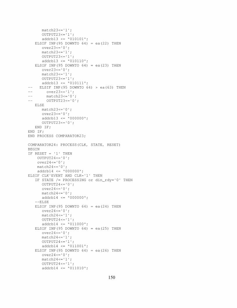
match23<='1'; OUTPUT23<='1'; addrb13 <= "010101"; ELSIF INP(95 DOWNTO 64) = ea(22) THEN over23<='0'; match23<='1'; OUTPUT23<='1'; addrb13 <= "010110"; ELSIF INP(95 DOWNTO 64) = ea(23) THEN over23<='0'; match23<='1'; OUTPUT23<='1'; addrb13 <= "010111"; -- ELSIF INP(95 DOWNTO 64) > ea(63) THEN -- over23<='1'; -- match23<='0'; -- OUTPUT23<='0'; ELSE match23<='0'; over23<='0'; addrb13 <= "000000"; OUTPUT23<='0'; END IF; END IF; END PROCESS COMPARATOR23; COMPARATOR24: PROCESS(CLK, STATE, RESET) BEGIN IF RESET = '1' THEN OUTPUT24<='0'; over24<='0'; match24<='0'; addrb14 <= "000000"; ELSIF CLK'EVENT AND CLK='1' THEN IF STATE /= PROCESSING or din_rdy='0' THEN OUTPUT24<='0'; over24<='0'; match24<='0'; addrb14 <= "000000"; --ELSE ELSIF INP(95 DOWNTO 64) = ea(24) THEN over24<='0'; match24<='1'; OUTPUT24<='1'; addrb14 <= "011000"; ELSIF INP(95 DOWNTO 64) = ea(25) THEN over24<='0'; match24<='1'; OUTPUT24<='1'; addrb14 <= "011001"; ELSIF INP(95 DOWNTO 64) = ea(26) THEN over24<='0'; match24<='1'; OUTPUT24<='1'; addrb14 <= "011010";
150
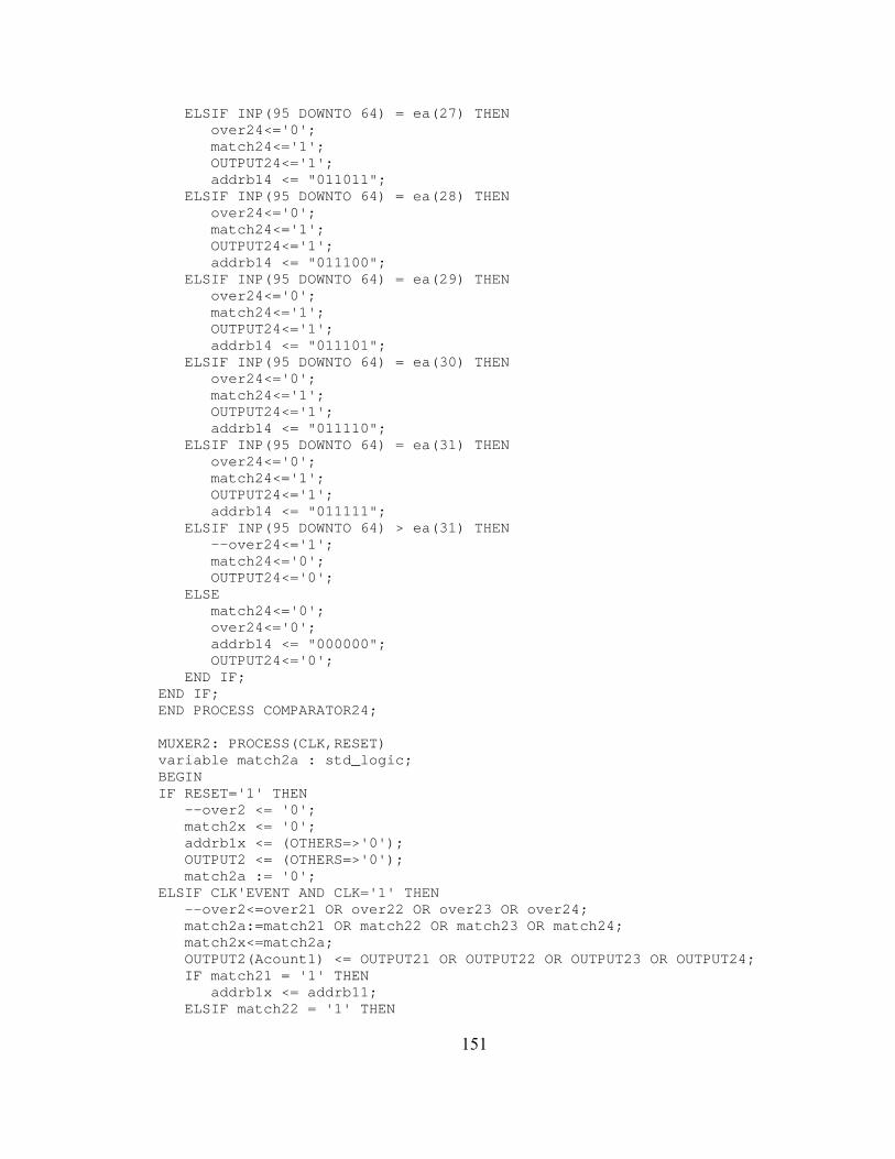
ELSIF INP(95 DOWNTO 64) = ea(27) THEN over24<='0'; match24<='1'; OUTPUT24<='1'; addrb14 <= "011011"; ELSIF INP(95 DOWNTO 64) = ea(28) THEN over24<='0'; match24<='1'; OUTPUT24<='1'; addrb14 <= "011100"; ELSIF INP(95 DOWNTO 64) = ea(29) THEN over24<='0'; match24<='1'; OUTPUT24<='1'; addrb14 <= "011101"; ELSIF INP(95 DOWNTO 64) = ea(30) THEN over24<='0'; match24<='1'; OUTPUT24<='1'; addrb14 <= "011110"; ELSIF INP(95 DOWNTO 64) = ea(31) THEN over24<='0'; match24<='1'; OUTPUT24<='1'; addrb14 <= "011111"; ELSIF INP(95 DOWNTO 64) > ea(31) THEN --over24<='1'; match24<='0'; OUTPUT24<='0'; ELSE match24<='0'; over24<='0'; addrb14 <= "000000"; OUTPUT24<='0'; END IF; END IF; END PROCESS COMPARATOR24; MUXER2: PROCESS(CLK,RESET) variable match2a : std_logic; BEGIN IF RESET='1' THEN --over2 <= '0'; match2x <= '0'; addrb1x <= (OTHERS=>'0'); OUTPUT2 <= (OTHERS=>'0'); match2a := '0'; ELSIF CLK'EVENT AND CLK='1' THEN --over2<=over21 OR over22 OR over23 OR over24; match2a:=match21 OR match22 OR match23 OR match24; match2x<=match2a; OUTPUT2(Acount1) <= OUTPUT21 OR OUTPUT22 OR OUTPUT23 OR OUTPUT24; IF match21 = '1' THEN addrb1x <= addrb11; ELSIF match22 = '1' THEN
151
addrb1x <= addrb12; ELSIF match23 = '1' THEN addrb1x <= addrb13; ELSIF match24 = '1' THEN addrb1x <= addrb14; ELSE addrb1x <= (OTHERS=>'0'); END IF; END IF; END PROCESS MUXER2; COMPARATOR31: PROCESS(CLK, STATE, RESET) BEGIN IF RESET = '1' THEN OUTPUT31<='0'; over31<='0'; match31<='0'; addra21 <= "000000"; ELSIF CLK'EVENT AND CLK='1' THEN IF STATE /= PROCESSING or din_rdy='0' THEN OUTPUT31<='0'; over31<='0'; match31<='0'; addra21 <= "000000"; --ELSE ELSIF INP(63 DOWNTO 32) = ea(0) THEN over31<='0'; match31<='1'; OUTPUT31<='1'; addra21 <= "000000"; ELSIF INP(63 DOWNTO 32) = ea(1) THEN over31<='0'; match31<='1'; OUTPUT31<='1'; addra21 <= "000001"; ELSIF INP(63 DOWNTO 32) = ea(2) THEN over31<='0'; match31<='1'; OUTPUT31<='1'; addra21 <= "000010"; ELSIF INP(63 DOWNTO 32) = ea(3) THEN over31<='0'; match31<='1'; OUTPUT31<='1'; addra21 <= "000011"; ELSIF INP(63 DOWNTO 32) = ea(4) THEN over31<='0'; match31<='1'; OUTPUT31<='1'; addra21 <= "000100"; ELSIF INP(63 DOWNTO 32) = ea(5) THEN over31<='0'; match31<='1'; OUTPUT31<='1'; addra21 <= "000101";
152
ELSIF INP(63 DOWNTO 32) = ea(6) THEN over31<='0'; match31<='1'; OUTPUT31<='1'; addra21 <= "000110"; ELSIF INP(63 DOWNTO 32) = ea(7) THEN over31<='0'; match31<='1'; OUTPUT31<='1'; addra21 <= "000111"; -- ELSIF INP(63 DOWNTO 32) > ea(63) THEN -- over31<='1'; -- match31<='0'; -- OUTPUT31<='0'; ELSE match31<='0'; over31<='0'; addra21 <= "000000"; OUTPUT31<='0'; END IF; END IF; END PROCESS COMPARATOR31; COMPARATOR32: PROCESS(CLK, STATE, RESET) BEGIN IF RESET = '1' THEN OUTPUT32<='0'; over32<='0'; match32<='0'; addra22 <= "000000"; ELSIF CLK'EVENT AND CLK='1' THEN IF STATE /= PROCESSING or din_rdy='0' THEN OUTPUT32<='0'; over32<='0'; match32<='0'; addra22 <= "000000"; --ELSE ELSIF INP(63 DOWNTO 32) = ea(8) THEN over32<='0'; match32<='1'; OUTPUT32<='1'; addra22 <= "001000"; ELSIF INP(63 DOWNTO 32) = ea(9) THEN over32<='0'; match32<='1'; OUTPUT32<='1'; addra22 <= "001001"; ELSIF INP(63 DOWNTO 32) = ea(10) THEN over32<='0'; match32<='1'; OUTPUT32<='1'; addra22 <= "001010"; ELSIF INP(63 DOWNTO 32) = ea(11) THEN over32<='0'; match32<='1';
153
OUTPUT32<='1'; addra22 <= "001011"; ELSIF INP(63 DOWNTO 32) = ea(12) THEN over32<='0'; match32<='1'; OUTPUT32<='1'; addra22 <= "001100"; ELSIF INP(63 DOWNTO 32) = ea(13) THEN over32<='0'; match32<='1'; OUTPUT32<='1'; addra22 <= "001101"; ELSIF INP(63 DOWNTO 32) = ea(14) THEN over32<='0'; match32<='1'; OUTPUT32<='1'; addra22 <= "001110"; ELSIF INP(63 DOWNTO 32) = ea(15) THEN over32<='0'; match32<='1'; OUTPUT32<='1'; addra22 <= "001111"; -- ELSIF INP(63 DOWNTO 32) > ea(63) THEN -- over32<='1'; -- match32<='0'; -- OUTPUT32<='0'; ELSE match32<='0'; over32<='0'; addra22 <= "000000"; OUTPUT32<='0'; END IF; END IF; END PROCESS COMPARATOR32; COMPARATOR33: PROCESS(CLK, STATE, RESET) BEGIN IF RESET = '1' THEN OUTPUT33<='0'; over33<='0'; match33<='0'; addra23 <= "000000"; ELSIF CLK'EVENT AND CLK='1' THEN IF STATE /= PROCESSING or din_rdy='0' THEN OUTPUT33<='0'; over33<='0'; match33<='0'; addra23 <= "000000"; --ELSE ELSIF INP(63 DOWNTO 32) = ea(16) THEN over33<='0'; match33<='1'; OUTPUT33<='1'; addra23 <= "010000"; ELSIF INP(63 DOWNTO 32) = ea(17) THEN
154
over33<='0'; match33<='1'; OUTPUT33<='1'; addra23 <= "010001"; ELSIF INP(63 DOWNTO 32) = ea(18) THEN over33<='0'; match33<='1'; OUTPUT33<='1'; addra23 <= "010010"; ELSIF INP(63 DOWNTO 32) = ea(19) THEN over33<='0'; match33<='1'; OUTPUT33<='1'; addra23 <= "010011"; ELSIF INP(63 DOWNTO 32) = ea(20) THEN over33<='0'; match33<='1'; OUTPUT33<='1'; addra23 <= "010100"; ELSIF INP(63 DOWNTO 32) = ea(21) THEN over33<='0'; match33<='1'; OUTPUT33<='1'; addra23 <= "010101"; ELSIF INP(63 DOWNTO 32) = ea(22) THEN over33<='0'; match33<='1'; OUTPUT33<='1'; addra23 <= "010110"; ELSIF INP(63 DOWNTO 32) = ea(23) THEN over33<='0'; match33<='1'; OUTPUT33<='1'; addra23 <= "010111"; -- ELSIF INP(63 DOWNTO 32) > ea(63) THEN -- over33<='1'; -- match33<='0'; -- OUTPUT33<='0'; ELSE match33<='0'; over33<='0'; addra23 <= "000000"; OUTPUT33<='0'; END IF; END IF; END PROCESS COMPARATOR33; COMPARATOR34: PROCESS(CLK, STATE, RESET) BEGIN IF RESET = '1' THEN OUTPUT34<='0'; over34<='0'; match34<='0'; addra24 <= "000000"; ELSIF CLK'EVENT AND CLK='1' THEN
155
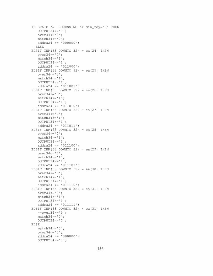
IF STATE /= PROCESSING or din_rdy='0' THEN OUTPUT34<='0'; over34<='0'; match34<='0'; addra24 <= "000000"; --ELSE ELSIF INP(63 DOWNTO 32) = ea(24) THEN over34<='0'; match34<='1'; OUTPUT34<='1'; addra24 <= "011000"; ELSIF INP(63 DOWNTO 32) = ea(25) THEN over34<='0'; match34<='1'; OUTPUT34<='1'; addra24 <= "011001"; ELSIF INP(63 DOWNTO 32) = ea(26) THEN over34<='0'; match34<='1'; OUTPUT34<='1'; addra24 <= "011010"; ELSIF INP(63 DOWNTO 32) = ea(27) THEN over34<='0'; match34<='1'; OUTPUT34<='1'; addra24 <= "011011"; ELSIF INP(63 DOWNTO 32) = ea(28) THEN over34<='0'; match34<='1'; OUTPUT34<='1'; addra24 <= "011100"; ELSIF INP(63 DOWNTO 32) = ea(29) THEN over34<='0'; match34<='1'; OUTPUT34<='1'; addra24 <= "011101"; ELSIF INP(63 DOWNTO 32) = ea(30) THEN over34<='0'; match34<='1'; OUTPUT34<='1'; addra24 <= "011110"; ELSIF INP(63 DOWNTO 32) = ea(31) THEN over34<='0'; match34<='1'; OUTPUT34<='1'; addra24 <= "011111"; ELSIF INP(63 DOWNTO 32) > ea(31) THEN --over34<='1'; match34<='0'; OUTPUT34<='0'; ELSE match34<='0'; over34<='0'; addra24 <= "000000"; OUTPUT34<='0';
156
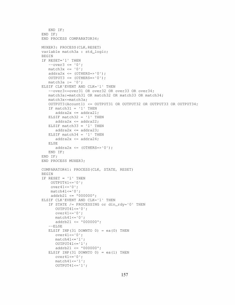
END IF; END IF; END PROCESS COMPARATOR34; MUXER3: PROCESS(CLK,RESET) variable match3a : std_logic; BEGIN IF RESET='1' THEN --over3 <= '0'; match3x <= '0'; addra2x <= (OTHERS=>'0'); OUTPUT3 <= (OTHERS=>'0'); match3a := '0'; ELSIF CLK'EVENT AND CLK='1' THEN --over3<=over31 OR over32 OR over33 OR over34; match3a:=match31 OR match32 OR match33 OR match34; match3x<=match3a; OUTPUT3(Acount1) <= OUTPUT31 OR OUTPUT32 OR OUTPUT33 OR OUTPUT34; IF match31 = '1' THEN addra2x <= addra21; ELSIF match32 = '1' THEN addra2x <= addra22; ELSIF match33 = '1' THEN addra2x <= addra23; ELSIF match34 = '1' THEN addra2x <= addra24; ELSE addra2x <= (OTHERS=>'0'); END IF; END IF; END PROCESS MUXER3; COMPARATOR41: PROCESS(CLK, STATE, RESET) BEGIN IF RESET = '1' THEN OUTPUT41<='0'; over41<='0'; match41<='0'; addrb21 <= "000000"; ELSIF CLK'EVENT AND CLK='1' THEN IF STATE /= PROCESSING or din_rdy='0' THEN OUTPUT41<='0'; over41<='0'; match41<='0'; addrb21 <= "000000"; --ELSE ELSIF INP(31 DOWNTO 0) = ea(0) THEN over41<='0'; match41<='1'; OUTPUT41<='1'; addrb21 <= "000000"; ELSIF INP(31 DOWNTO 0) = ea(1) THEN over41<='0'; match41<='1'; OUTPUT41<='1';
157
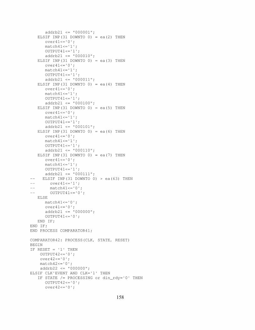
addrb21 <= "000001"; ELSIF INP(31 DOWNTO 0) = ea(2) THEN over41<='0'; match41<='1'; OUTPUT41<='1'; addrb21 <= "000010"; ELSIF INP(31 DOWNTO 0) = ea(3) THEN over41<='0'; match41<='1'; OUTPUT41<='1'; addrb21 <= "000011"; ELSIF INP(31 DOWNTO 0) = ea(4) THEN over41<='0'; match41<='1'; OUTPUT41<='1'; addrb21 <= "000100"; ELSIF INP(31 DOWNTO 0) = ea(5) THEN over41<='0'; match41<='1'; OUTPUT41<='1'; addrb21 <= "000101"; ELSIF INP(31 DOWNTO 0) = ea(6) THEN over41<='0'; match41<='1'; OUTPUT41<='1'; addrb21 <= "000110"; ELSIF INP(31 DOWNTO 0) = ea(7) THEN over41<='0'; match41<='1'; OUTPUT41<='1'; addrb21 <= "000111"; -- ELSIF INP(31 DOWNTO 0) > ea(63) THEN -- over41<='1'; -- match41<='0'; -- OUTPUT41<='0'; ELSE match41<='0'; over41<='0'; addrb21 <= "000000"; OUTPUT41<='0'; END IF; END IF; END PROCESS COMPARATOR41; COMPARATOR42: PROCESS(CLK, STATE, RESET) BEGIN IF RESET = '1' THEN OUTPUT42<='0'; over42<='0'; match42<='0'; addrb22 <= "000000"; ELSIF CLK'EVENT AND CLK='1' THEN IF STATE /= PROCESSING or din_rdy='0' THEN OUTPUT42<='0'; over42<='0';
158

match42<='0'; addrb22 <= "000000"; --ELSE ELSIF INP(31 DOWNTO 0) = ea(8) THEN over42<='0'; match42<='1'; OUTPUT42<='1'; addrb22 <= "001000"; ELSIF INP(31 DOWNTO 0) = ea(9) THEN over42<='0'; match42<='1'; OUTPUT42<='1'; addrb22 <= "001001"; ELSIF INP(31 DOWNTO 0) = ea(10) THEN over42<='0'; match42<='1'; OUTPUT42<='1'; addrb22 <= "001010"; ELSIF INP(31 DOWNTO 0) = ea(11) THEN over42<='0'; match42<='1'; OUTPUT42<='1'; addrb22 <= "001011"; ELSIF INP(31 DOWNTO 0) = ea(12) THEN over42<='0'; match42<='1'; OUTPUT42<='1'; addrb22 <= "001100"; ELSIF INP(31 DOWNTO 0) = ea(13) THEN over42<='0'; match42<='1'; OUTPUT42<='1'; addrb22 <= "001101"; ELSIF INP(31 DOWNTO 0) = ea(14) THEN over42<='0'; match42<='1'; OUTPUT42<='1'; addrb22 <= "001110"; ELSIF INP(31 DOWNTO 0) = ea(15) THEN over42<='0'; match42<='1'; OUTPUT42<='1'; addrb22 <= "001111"; -- ELSIF INP(31 DOWNTO 0) > ea(63) THEN -- over42<='1'; -- match42<='0'; -- OUTPUT42<='0'; ELSE match42<='0'; over42<='0'; addrb22 <= "000000"; OUTPUT42<='0'; END IF; END IF; END PROCESS COMPARATOR42;
159
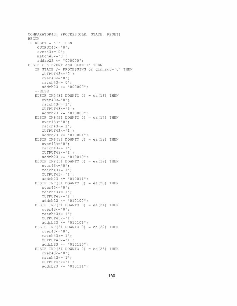
COMPARATOR43: PROCESS(CLK, STATE, RESET) BEGIN IF RESET = '1' THEN OUTPUT43<='0'; over43<='0'; match43<='0'; addrb23 <= "000000"; ELSIF CLK'EVENT AND CLK='1' THEN IF STATE /= PROCESSING or din_rdy='0' THEN OUTPUT43<='0'; over43<='0'; match43<='0'; addrb23 <= "000000"; --ELSE ELSIF INP(31 DOWNTO 0) = ea(16) THEN over43<='0'; match43<='1'; OUTPUT43<='1'; addrb23 <= "010000"; ELSIF INP(31 DOWNTO 0) = ea(17) THEN over43<='0'; match43<='1'; OUTPUT43<='1'; addrb23 <= "010001"; ELSIF INP(31 DOWNTO 0) = ea(18) THEN over43<='0'; match43<='1'; OUTPUT43<='1'; addrb23 <= "010010"; ELSIF INP(31 DOWNTO 0) = ea(19) THEN over43<='0'; match43<='1'; OUTPUT43<='1'; addrb23 <= "010011"; ELSIF INP(31 DOWNTO 0) = ea(20) THEN over43<='0'; match43<='1'; OUTPUT43<='1'; addrb23 <= "010100"; ELSIF INP(31 DOWNTO 0) = ea(21) THEN over43<='0'; match43<='1'; OUTPUT43<='1'; addrb23 <= "010101"; ELSIF INP(31 DOWNTO 0) = ea(22) THEN over43<='0'; match43<='1'; OUTPUT43<='1'; addrb23 <= "010110"; ELSIF INP(31 DOWNTO 0) = ea(23) THEN over43<='0'; match43<='1'; OUTPUT43<='1'; addrb23 <= "010111";
160
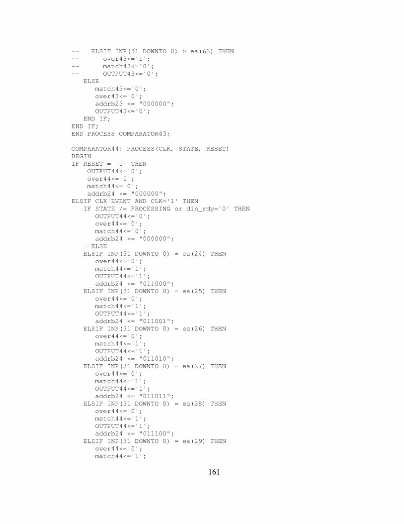
-- ELSIF INP(31 DOWNTO 0) > ea(63) THEN -- over43<='1'; -- match43<='0'; -- OUTPUT43<='0'; ELSE match43<='0'; over43<='0'; addrb23 <= "000000"; OUTPUT43<='0'; END IF; END IF; END PROCESS COMPARATOR43; COMPARATOR44: PROCESS(CLK, STATE, RESET) BEGIN IF RESET = '1' THEN OUTPUT44<='0'; over44<='0'; match44<='0'; addrb24 <= "000000"; ELSIF CLK'EVENT AND CLK='1' THEN IF STATE /= PROCESSING or din_rdy='0' THEN OUTPUT44<='0'; over44<='0'; match44<='0'; addrb24 <= "000000"; --ELSE ELSIF INP(31 DOWNTO 0) = ea(24) THEN over44<='0'; match44<='1'; OUTPUT44<='1'; addrb24 <= "011000"; ELSIF INP(31 DOWNTO 0) = ea(25) THEN over44<='0'; match44<='1'; OUTPUT44<='1'; addrb24 <= "011001"; ELSIF INP(31 DOWNTO 0) = ea(26) THEN over44<='0'; match44<='1'; OUTPUT44<='1'; addrb24 <= "011010"; ELSIF INP(31 DOWNTO 0) = ea(27) THEN over44<='0'; match44<='1'; OUTPUT44<='1'; addrb24 <= "011011"; ELSIF INP(31 DOWNTO 0) = ea(28) THEN over44<='0'; match44<='1'; OUTPUT44<='1'; addrb24 <= "011100"; ELSIF INP(31 DOWNTO 0) = ea(29) THEN over44<='0'; match44<='1';
161
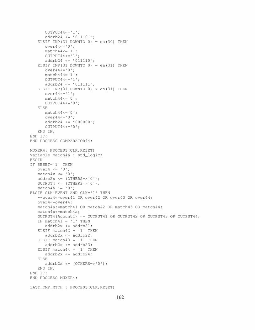
OUTPUT44<='1'; addrb24 <= "011101"; ELSIF INP(31 DOWNTO 0) = ea(30) THEN over44<='0'; match44<='1'; OUTPUT44<='1'; addrb24 <= "011110"; ELSIF INP(31 DOWNTO 0) = ea(31) THEN over44<='0'; match44<='1'; OUTPUT44<='1'; addrb24 <= "011111"; ELSIF INP(31 DOWNTO 0) > ea(31) THEN over44<='1'; match44<='0'; OUTPUT44<='0'; ELSE match44<='0'; over44<='0'; addrb24 <= "000000"; OUTPUT44<='0'; END IF; END IF; END PROCESS COMPARATOR44; MUXER4: PROCESS(CLK,RESET) variable match4a : std_logic; BEGIN IF RESET='1' THEN over4 <= '0'; match4x <= '0'; addrb2x <= (OTHERS=>'0'); OUTPUT4 <= (OTHERS=>'0'); match4a := '0'; ELSIF CLK'EVENT AND CLK='1' THEN --over4<=over41 OR over42 OR over43 OR over44; over4<=over44; match4a:=match41 OR match42 OR match43 OR match44; match4x<=match4a; OUTPUT4(Acount1) <= OUTPUT41 OR OUTPUT42 OR OUTPUT43 OR OUTPUT44; IF match41 = '1' THEN addrb2x <= addrb21; ELSIF match42 = '1' THEN addrb2x <= addrb22; ELSIF match43 = '1' THEN addrb2x <= addrb23; ELSIF match44 = '1' THEN addrb2x <= addrb24; ELSE addrb2x <= (OTHERS=>'0'); END IF; END IF; END PROCESS MUXER4; LAST_CMP_MTCH : PROCESS(CLK,RESET)
162
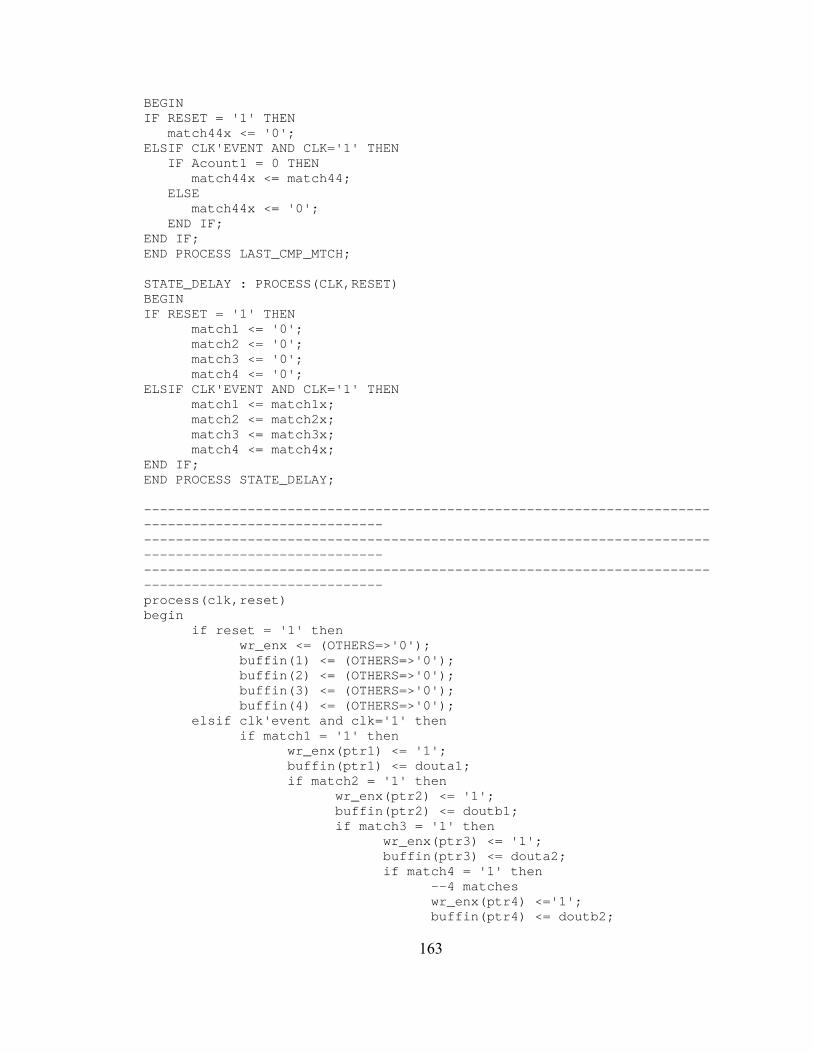
BEGIN IF RESET = '1' THEN match44x <= '0'; ELSIF CLK'EVENT AND CLK='1' THEN IF Acount1 = 0 THEN match44x <= match44; ELSE match44x <= '0'; END IF; END IF; END PROCESS LAST_CMP_MTCH; STATE_DELAY : PROCESS(CLK,RESET) BEGIN IF RESET = '1' THEN match1 <= '0'; match2 <= '0'; match3 <= '0'; match4 <= '0'; ELSIF CLK'EVENT AND CLK='1' THEN match1 <= match1x; match2 <= match2x; match3 <= match3x; match4 <= match4x; END IF; END PROCESS STATE_DELAY; ----------------------------------------------------------------------------------------------------- ----------------------------------------------------------------------------------------------------- ----------------------------------------------------------------------------------------------------- process(clk,reset) begin if reset = '1' then wr_enx <= (OTHERS=>'0'); buffin(1) <= (OTHERS=>'0'); buffin(2) <= (OTHERS=>'0'); buffin(3) <= (OTHERS=>'0'); buffin(4) <= (OTHERS=>'0'); elsif clk'event and clk='1' then if match1 = '1' then wr_enx(ptr1) <= '1'; buffin(ptr1) <= douta1; if match2 = '1' then wr_enx(ptr2) <= '1'; buffin(ptr2) <= doutb1; if match3 = '1' then wr_enx(ptr3) <= '1'; buffin(ptr3) <= douta2; if match4 = '1' then --4 matches wr_enx(ptr4) <='1'; buffin(ptr4) <= doutb2;
163
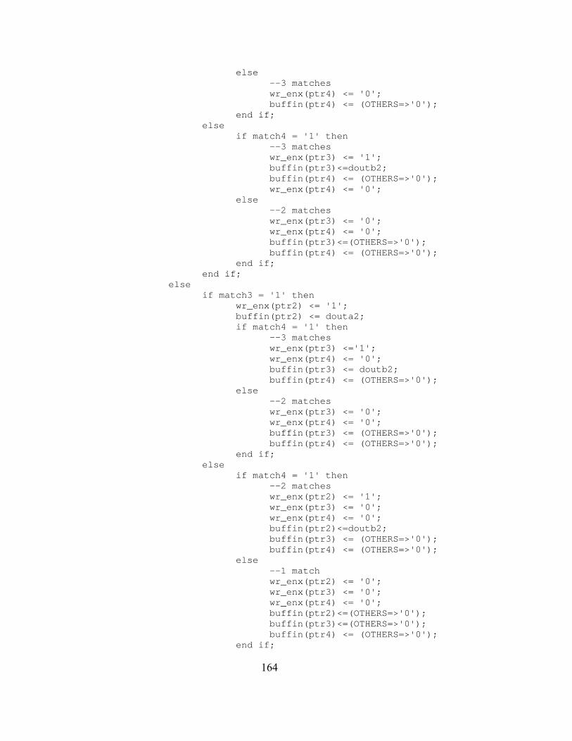
else --3 matches wr_enx(ptr4) <= '0'; buffin(ptr4) <= (OTHERS=>'0'); end if; else if match4 = '1' then --3 matches wr_enx(ptr3) <= '1'; buffin(ptr3)<=doutb2; buffin(ptr4) <= (OTHERS=>'0'); wr_enx(ptr4) <= '0'; else --2 matches wr_enx(ptr3) <= '0'; wr_enx(ptr4) <= '0'; buffin(ptr3)<=(OTHERS=>'0'); buffin(ptr4) <= (OTHERS=>'0'); end if; end if; else if match3 = '1' then wr_enx(ptr2) <= '1'; buffin(ptr2) <= douta2; if match4 = '1' then --3 matches wr_enx(ptr3) <='1'; wr_enx(ptr4) <= '0'; buffin(ptr3) <= doutb2; buffin(ptr4) <= (OTHERS=>'0'); else --2 matches wr_enx(ptr3) <= '0'; wr_enx(ptr4) <= '0'; buffin(ptr3) <= (OTHERS=>'0'); buffin(ptr4) <= (OTHERS=>'0'); end if; else if match4 = '1' then --2 matches wr_enx(ptr2) <= '1'; wr_enx(ptr3) <= '0'; wr_enx(ptr4) <= '0'; buffin(ptr2)<=doutb2; buffin(ptr3) <= (OTHERS=>'0'); buffin(ptr4) <= (OTHERS=>'0'); else --1 match wr_enx(ptr2) <= '0'; wr_enx(ptr3) <= '0'; wr_enx(ptr4) <= '0'; buffin(ptr2)<=(OTHERS=>'0'); buffin(ptr3)<=(OTHERS=>'0'); buffin(ptr4) <= (OTHERS=>'0'); end if;
164
end if; end if; else if match2 = '1' then wr_enx(ptr1) <= '1'; buffin(ptr1) <= doutb1; if match3 = '1' then wr_enx(ptr2) <= '1'; buffin(ptr2) <= douta2; if match4 = '1' then --3 matches wr_enx(ptr3) <= '1'; wr_enx(ptr4) <= '0'; buffin(ptr3) <= doutb2; buffin(ptr4) <= (OTHERS=>'0'); else --2 matches wr_enx(ptr3) <= '0'; wr_enx(ptr4) <= '0'; buffin(ptr3) <= (OTHERS=>'0'); buffin(ptr4) <= (OTHERS=>'0'); end if; else if match4 = '1' then --2 matches wr_enx(ptr2) <= '1'; wr_enx(ptr3) <= '0'; wr_enx(ptr4) <= '0'; buffin(ptr2) <= doutb2; buffin(ptr3) <= (OTHERS=>'0'); buffin(ptr4) <= (OTHERS=>'0'); else --1 match wr_enx(ptr2) <= '0'; wr_enx(ptr3) <= '0'; wr_enx(ptr4) <= '0'; buffin(ptr2) <= (OTHERS=>'0'); buffin(ptr3) <= (OTHERS=>'0'); buffin(ptr4) <= (OTHERS=>'0'); end if; end if; else if match3 = '1' then wr_enx(ptr1) <= '1'; buffin(ptr1) <= douta2; if match4 = '1' then --2 matches wr_enx(ptr2) <= '1'; wr_enx(ptr3) <= '0'; wr_enx(ptr4) <= '0'; buffin(ptr2) <= doutb2; buffin(ptr3) <= (OTHERS=>'0'); buffin(ptr4) <= (OTHERS=>'0'); else --1 match
165
wr_enx(ptr2) <= '0'; wr_enx(ptr3) <= '0'; wr_enx(ptr4) <= '0'; buffin(ptr2) <= (OTHERS=>'0'); buffin(ptr3) <= (OTHERS=>'0'); buffin(ptr4) <= (OTHERS=>'0'); end if; else if match4 = '1' then --1 match wr_enx(ptr1) <= '1'; wr_enx(ptr2) <= '0'; wr_enx(ptr3) <= '0'; wr_enx(ptr4) <= '0'; buffin(ptr1) <= doutb2; buffin(ptr2) <= (OTHERS=>'0'); buffin(ptr3) <= (OTHERS=>'0'); buffin(ptr4) <= (OTHERS=>'0'); else --0 matches wr_enx(ptr1) <= '0'; wr_enx(ptr2) <= '0'; wr_enx(ptr3) <= '0'; wr_enx(ptr4) <= '0'; buffin(ptr1) <= (OTHERS=>'0'); buffin(ptr2) <= (OTHERS=>'0'); buffin(ptr3) <= (OTHERS=>'0'); buffin(ptr4) <= (OTHERS=>'0'); end if; end if; end if; end if; end if; end process; process(clk,reset) variable g,h,j,f : std_logic; begin if reset = '1' then ptr1 <= 1; elsif clk'event and clk='1' then --mx1a := match1 NOR match2 NOR match3; --mx1b := match1 NOR match2 NOR match4; --mx1c := match1 NOR match3 NOR match4; --mx1d := match2 NOR match3 NOR match4; --match1 AND match2 --match1 AND match3 --match1 AND match4 --match2 AND match3 --match2 AND match4 --match3 AND match4 --match1 AND match2 AND match3;
166
--match1 AND match2 AND match4; --match1 AND match3 AND match4; --match2 AND match3 AND match4; --j := g NOR h; --j := NOR(g,h); --j := NOR3(g,h,f); --j := g NOR h NOR f; if STATE_DEL = REPORTx then ptr1 <= 1; elsif (match1 AND match2 AND match3 AND match4)='1' then --4 match --do nothing ptr1 <= ptr1; elsif ((match1 AND match2 AND match3)OR(match1 AND match2 AND match4)OR(match1 AND match3 AND match4)OR(match2 AND match3 AND match4))='1' then --3 match if ptr1 = 2 then ptr1 <= 1; elsif ptr1 = 3 then ptr1 <= 2; elsif ptr1 = 4 then ptr1 <= 3; else ptr1 <= 4; end if; elsif ((match1 AND match2)OR(match1 AND match3)OR(match1 AND match4)OR(match2 AND match3)OR(match2 AND match4)OR(match3 AND match4))='1' then --2 match if ptr1 = 3 then ptr1 <= 1; elsif ptr1 = 4 then ptr1 <= 2; elsif ptr1 = 2 then ptr1 <= 4; else ptr1 <= 3; end if; elsif (match1 OR match2 OR match3 OR match4)='0' then --0 matches do nothing else --1 match if ptr1 = 4 then ptr1 <= 1; elsif ptr1 = 3 then ptr1 <= 4; elsif ptr1 = 2 then ptr1 <= 3; else ptr1 <= 2; end if; end if; end if;
167
end process; process(clk,reset) begin if reset = '1' then ptr2 <= 2; elsif clk'event and clk='1' then if STATE_DEL = REPORTx then ptr2 <= 2; elsif (match1 AND match2 AND match3 AND match4)='1' then --4 match --do nothing ptr2 <= ptr2; elsif ((match1 AND match2 AND match3)OR(match1 AND match2 AND match4)OR(match1 AND match3 AND match4)OR(match2 AND match3 AND match4))='1' then --3 match if ptr2 = 2 then ptr2 <= 1; elsif ptr2 = 3 then ptr2 <= 2; elsif ptr2 = 4 then ptr2 <= 3; else ptr2 <= 4; end if; elsif ((match1 AND match2)OR(match1 AND match3)OR(match1 AND match4)OR(match2 AND match3)OR(match2 AND match4)OR(match3 AND match4))='1' then --2 match if ptr2 = 3 then ptr2 <= 1; elsif ptr2 = 4 then ptr2 <= 2; elsif ptr2 = 1 then ptr2 <= 3; else ptr2 <= 4; end if; elsif (match1 OR match2 OR match3 OR match4)='0' then --0 matches do nothing else --1 match if ptr2 = 4 then ptr2 <= 1; elsif ptr2 = 3 then ptr2 <= 4; elsif ptr2 = 2 then ptr2 <= 3; else ptr2 <= 2; end if; end if; end if; end process; process(clk,reset)
168
begin if reset = '1' then ptr3 <= 3; elsif clk'event and clk='1' then if STATE_DEL = REPORTx then ptr3 <= 3; elsif (match1 AND match2 AND match3 AND match4)='1' then --4 match --do nothing ptr3 <= ptr3; elsif ((match1 AND match2 AND match3)OR(match1 AND match2 AND match4)OR(match1 AND match3 AND match4)OR(match2 AND match3 AND match4))='1' then --3 match if ptr3 = 2 then ptr3 <= 1; elsif ptr3 = 3 then ptr3 <= 2; elsif ptr3 = 4 then ptr3 <= 3; else ptr3 <= 4; end if; elsif ((match1 AND match2)OR(match1 AND match3)OR(match1 AND match4)OR(match2 AND match3)OR(match2 AND match4)OR(match3 AND match4))='1' then --2 match if ptr3 = 3 then ptr3 <= 1; elsif ptr3 = 2 then ptr3 <= 4; elsif ptr3 = 1 then ptr3 <= 3; else ptr3 <= 2; end if; elsif (match1 OR match2 OR match3 OR match4)='0' then --0 matches do nothing else --1 match if ptr3 = 4 then ptr3 <= 1; elsif ptr3 = 3 then ptr3 <= 4; elsif ptr3 = 2 then ptr3 <= 3; else ptr3 <= 2; end if; end if; end if; end process; process(clk,reset) begin if reset = '1' then
169
ptr4 <= 4; elsif clk'event and clk='1' then if STATE_DEL = REPORTx then ptr4 <= 4; elsif (match1 AND match2 AND match3 AND match4)='1' then --4 match --do nothing ptr4 <= ptr4; elsif ((match1 AND match2 AND match3)OR(match1 AND match2 AND match4)OR(match1 AND match3 AND match4)OR(match2 AND match3 AND match4))='1' then --3 match if ptr4 = 2 then ptr4 <= 1; elsif ptr4 = 3 then ptr4 <= 2; elsif ptr4 = 4 then ptr4 <= 3; else ptr4 <= 4; end if; elsif ((match1 AND match2)OR(match1 AND match3)OR(match1 AND match4)OR(match2 AND match3)OR(match2 AND match4)OR(match3 AND match4))='1' then --2 match if ptr4 = 3 then ptr4 <= 1; elsif ptr4 = 2 then ptr4 <= 4; elsif ptr4 = 1 then ptr4 <= 3; else ptr4 <= 2; end if; elsif (match1 OR match2 OR match3 OR match4)='0' then --0 matches do nothing else --1 match if ptr4 = 4 then ptr4 <= 1; elsif ptr4 = 3 then ptr4 <= 4; elsif ptr4 = 2 then ptr4 <= 3; else ptr4 <= 2; end if; end if; end if; end process; process(clk,reset) begin if reset = '1' then sm1a <= '0';
170
sm1b <= '0'; --sm1 <= '0'; side1 <= '0'; side1a <= '0'; side1b <= '0'; Aa <= (OTHERS=>'0'); Ab <= (OTHERS=>'0'); Mult_in1A <= (OTHERS=>'0'); rd_en1<='0'; rd_en3<='0'; elsif clk'event and clk='1' then if STATE = REPORTx THEN side1 <= '0'; elsif din_rdy='1' and STATE_DEL=MACN AND INP/="00000000000000000000000000000000000000000000000000000000000000000000000000000000000000000000000000000000000000000000000000000000" then if side1 = '0' then if empty1='0' then sm1a <= '1'; rd_en1 <= '1'; rd_en3 <= '0'; Aa <= INP(127 DOWNTO 64); side1 <= '1'; elsif empty3='0' then sm1a <= '1'; rd_en1 <= '0'; rd_en3 <= '1'; Aa <= INP(127 DOWNTO 64); side1 <= '0'; else sm1a <= '0'; rd_en1 <= '0'; rd_en3 <= '0'; Aa <= (OTHERS=>'0'); side1 <= '0'; end if; else if empty3='0' then sm1a <= '1'; rd_en1 <= '0'; rd_en3 <= '1'; Aa <= INP(127 DOWNTO 64); side1 <= '0'; elsif empty1='0' then sm1a <= '1'; rd_en1 <= '1'; rd_en3 <= '0'; Aa <= INP(127 DOWNTO 64); side1 <= '0'; else sm1a <= '0'; rd_en1 <= '0'; rd_en3 <= '0'; Aa <= (OTHERS=>'0'); side1 <= '0';
171
end if; end if; else sm1a <= '0'; rd_en1 <= '0'; rd_en3 <= '0'; end if; sm1b <= sm1a; --sm1 <= sm1b; ----sm1 <= sm1a; Ab <= Aa; --Mult_in1A <= Ab; Mult_in1A <= Aa; side1a <= side1; side1b <= side1a; end if; end process; sm1 <= '0' when (rd_err1 OR rd_err3) = '1' else sm1b; sm2 <= '0' when (rd_err2 OR rd_err4) = '1' else sm2b; --Mult_in1B <= dout1 when side1a='0' else dout3; --Mult_in2B <= dout2 when side2a='0' else dout4; Mult_in1B <= dout1 when side1b='0' else dout3; Mult_in2B <= dout2 when side2b='0' else dout4; process(clk,reset) begin if reset = '1' then sm2a <= '0'; sm2b <= '0'; --sm2 <= '0'; side2 <= '0'; side2a <= '0'; side2b <= '0'; xa <= (OTHERS=>'0'); Xb <= (OTHERS=>'0'); Mult_in2A <= (OTHERS=>'0'); rd_en2<='0'; rd_en4<='0'; elsif clk'event and clk='1' then if STATE = PROCESSING THEN side2 <= '0'; elsif din_rdy='1' and STATE_DEL=MACN AND INP/="00000000000000000000000000000000000000000000000000000000000000000000000000000000000000000000000000000000000000000000000000000000" then if side2 = '0' then if empty2='0' then sm2a <= '1'; rd_en2 <= '1'; rd_en4 <= '0'; xa <= INP(63 DOWNTO 0); side2 <= '1'; elsif empty4='0' then sm2a <= '1'; rd_en2 <= '0'; rd_en4 <= '1'; xa <= INP(63 DOWNTO 0);
172
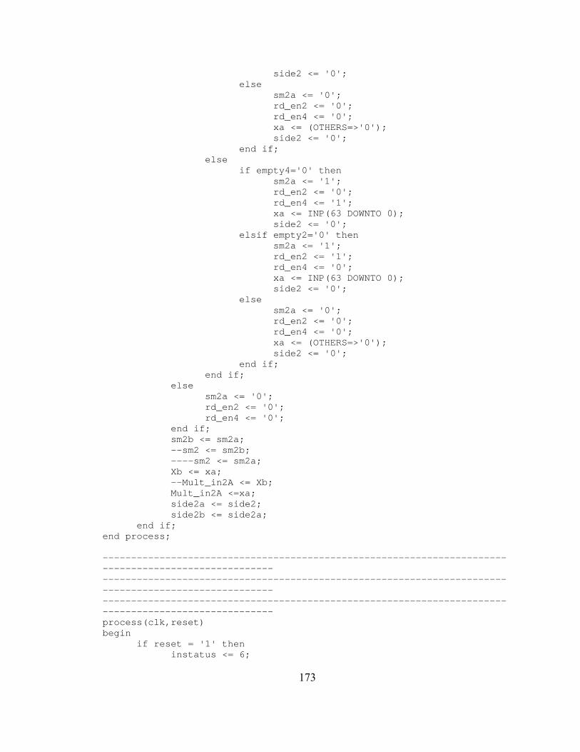
side2 <= '0'; else sm2a <= '0'; rd_en2 <= '0'; rd_en4 <= '0'; xa <= (OTHERS=>'0'); side2 <= '0'; end if; else if empty4='0' then sm2a <= '1'; rd_en2 <= '0'; rd_en4 <= '1'; xa <= INP(63 DOWNTO 0); side2 <= '0'; elsif empty2='0' then sm2a <= '1'; rd_en2 <= '1'; rd_en4 <= '0'; xa <= INP(63 DOWNTO 0); side2 <= '0'; else sm2a <= '0'; rd_en2 <= '0'; rd_en4 <= '0'; xa <= (OTHERS=>'0'); side2 <= '0'; end if; end if; else sm2a <= '0'; rd_en2 <= '0'; rd_en4 <= '0'; end if; sm2b <= sm2a; --sm2 <= sm2b; ----sm2 <= sm2a; Xb <= xa; --Mult_in2A <= Xb; Mult_in2A <=xa; side2a <= side2; side2b <= side2a; end if; end process; ----------------------------------------------------------------------------------------------------- ----------------------------------------------------------------------------------------------------- ----------------------------------------------------------------------------------------------------- process(clk,reset) begin if reset = '1' then instatus <= 6;
173
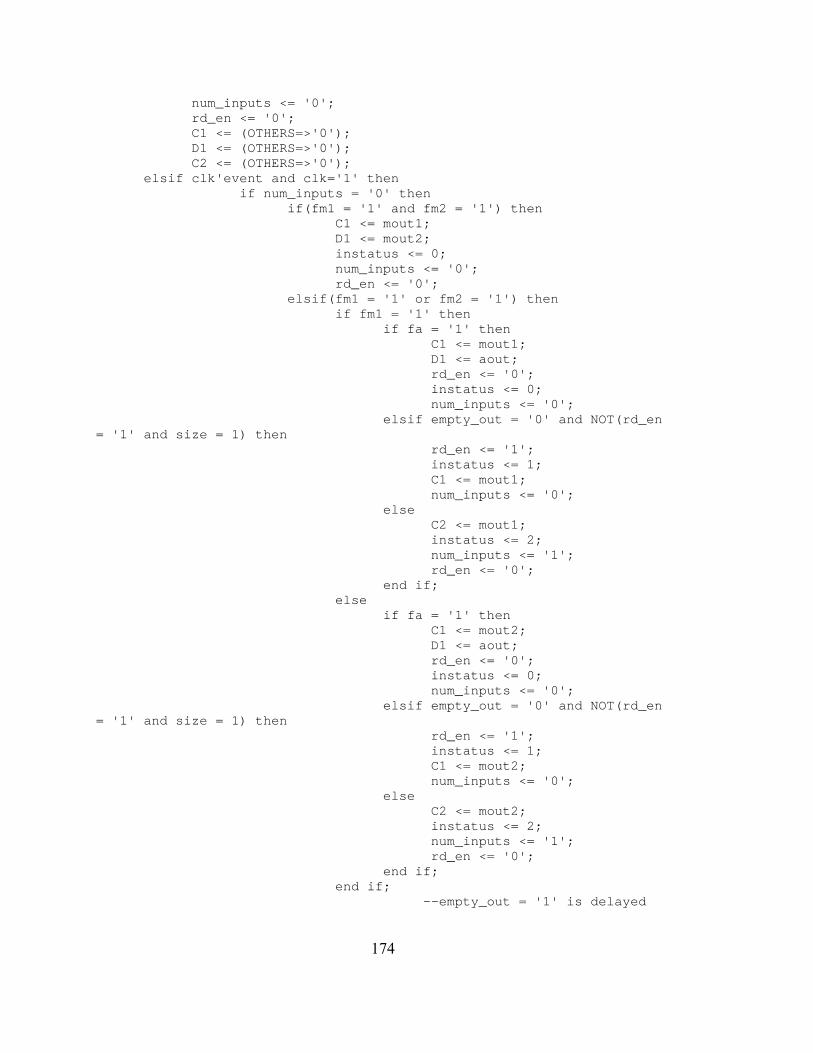
num_inputs <= '0'; rd_en <= '0'; C1 <= (OTHERS=>'0'); D1 <= (OTHERS=>'0'); C2 <= (OTHERS=>'0'); elsif clk'event and clk='1' then if num_inputs = '0' then if(fm1 = '1' and fm2 = '1') then C1 <= mout1; D1 <= mout2; instatus <= 0; num_inputs <= '0'; rd_en <= '0'; elsif(fm1 = '1' or fm2 = '1') then if fm1 = '1' then if fa = '1' then C1 <= mout1; D1 <= aout; rd_en <= '0'; instatus <= 0; num_inputs <= '0'; elsif empty_out = '0' and NOT(rd_en = '1' and size = 1) then rd_en <= '1'; instatus <= 1; C1 <= mout1; num_inputs <= '0'; else C2 <= mout1; instatus <= 2; num_inputs <= '1'; rd_en <= '0'; end if; else if fa = '1' then C1 <= mout2; D1 <= aout; rd_en <= '0'; instatus <= 0; num_inputs <= '0'; elsif empty_out = '0' and NOT(rd_en = '1' and size = 1) then rd_en <= '1'; instatus <= 1; C1 <= mout2; num_inputs <= '0'; else C2 <= mout2; instatus <= 2; num_inputs <= '1'; rd_en <= '0'; end if; end if; --empty_out = '1' is delayed
174
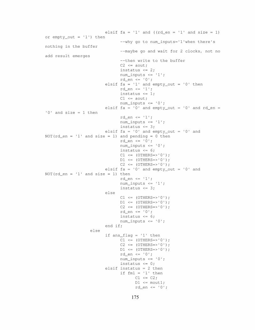
elsif fa = '1' and ((rd_en = '1' and size = 1) or empty_out = '1') then --why go to num_inputs='1'when there's nothing in the buffer --maybe go and wait for 2 clocks, not no add result emerges --then write to the buffer C2 <= aout; instatus <= 2; num_inputs <= '1'; rd_en <= '0'; elsif fa = '1' and empty_out = '0' then rd_en <= '1'; instatus <= 1; C1 <= aout; num_inputs <= '0'; elsif fa = '0' and empty_out = '0' and rd_en = '0' and size = 1 then rd_en <= '1'; num_inputs <= '1'; instatus <= 3; elsif fa = '0' and empty_out = '0' and NOT(rd_en = '1' and size = 1) and pending = 0 then rd_en <= '0'; num_inputs <= '0'; instatus <= 6; C1 <= (OTHERS=>'0'); D1 <= (OTHERS=>'0'); C2 <= (OTHERS=>'0'); elsif fa = '0' and empty_out = '0' and NOT(rd_en = '1' and size = 1) then rd_en <= '1'; num_inputs <= '1'; instatus <= 3; else C1 <= (OTHERS=>'0'); D1 <= (OTHERS=>'0'); C2 <= (OTHERS=>'0'); rd_en <= '0'; instatus <= 6; num_inputs <= '0'; end if; else if ans_flag = '1' then C1 <= (OTHERS=>'0'); C2 <= (OTHERS=>'0'); D1 <= (OTHERS=>'0'); rd_en <= '0'; num_inputs <= '0'; instatus <= 0; elsif instatus = 2 then if fm1 = '1' then C1 <= C2; D1 <= mout1; rd_en <= '0';
175
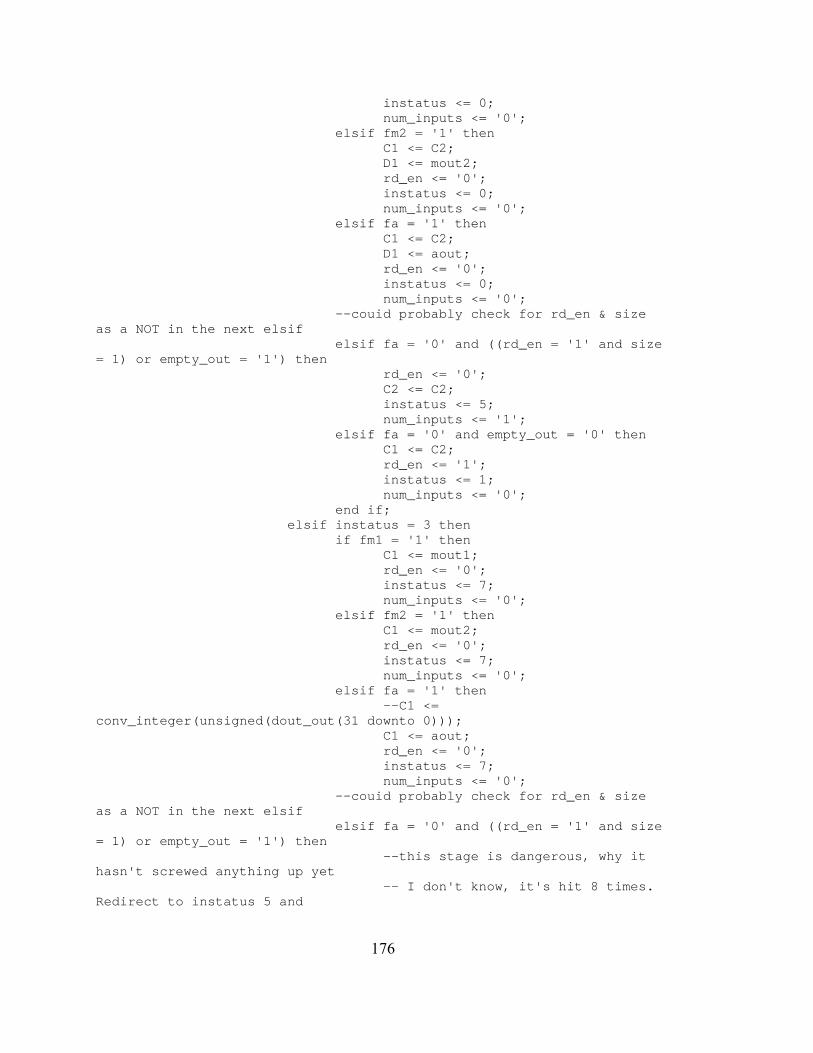
instatus <= 0; num_inputs <= '0'; elsif fm2 = '1' then C1 <= C2; D1 <= mout2; rd_en <= '0'; instatus <= 0; num_inputs <= '0'; elsif fa = '1' then C1 <= C2; D1 <= aout; rd_en <= '0'; instatus <= 0; num_inputs <= '0'; --couid probably check for rd_en & size as a NOT in the next elsif elsif fa = '0' and ((rd_en = '1' and size = 1) or empty_out = '1') then rd_en <= '0'; C2 <= C2; instatus <= 5; num_inputs <= '1'; elsif fa = '0' and empty_out = '0' then C1 <= C2; rd_en <= '1'; instatus <= 1; num_inputs <= '0'; end if; elsif instatus = 3 then if fm1 = '1' then C1 <= mout1; rd_en <= '0'; instatus <= 7; num_inputs <= '0'; elsif fm2 = '1' then C1 <= mout2; rd_en <= '0'; instatus <= 7; num_inputs <= '0'; elsif fa = '1' then --C1 <= conv_integer(unsigned(dout_out(31 downto 0))); C1 <= aout; rd_en <= '0'; instatus <= 7; num_inputs <= '0'; --couid probably check for rd_en & size as a NOT in the next elsif elsif fa = '0' and ((rd_en = '1' and size = 1) or empty_out = '1') then --this stage is dangerous, why it hasn't screwed anything up yet -- I don't know, it's hit 8 times. Redirect to instatus 5 and
176
-- have the buffer read back in the data. --rd_en <= '0'; --C2 <= C2; --instatus <= instatus; num_inputs <= '1'; rd_en <= '0'; instatus <= 9; elsif fa = '0' and empty_out = '0' then --C2 <= conv_integer(unsigned(dout_out(31 downto 0))); rd_en <= '1'; --instatus <= 8; num_inputs <= '1'; instatus <= 4; end if; elsif instatus = 4 then --C1 <= C2; C1 <= dout_out; instatus <= 7; num_inputs <= '0'; rd_en <= '0'; elsif instatus = 5 then if fm1 = '1' then C1 <= C2; D1 <= mout1; rd_en <= '0'; instatus <= 0; num_inputs <= '0'; elsif fm2 = '1' then C1 <= C2; D1 <= mout2; rd_en <= '0'; instatus <= 0; num_inputs <= '0'; elsif fa = '1' then C1 <= C2; D1 <= aout; rd_en <= '0'; instatus <= 0; num_inputs <= '0'; elsif rd_ack = '1' then --rewrite back into buffer C2 <= (OTHERS=>'0'); rd_en <= '0'; num_inputs <= '0'; C1 <= (OTHERS=>'0'); D1 <= (OTHERS=>'0'); instatus <= 6; else --write C2 to buffer and clear it C2 <= (OTHERS=>'0'); rd_en <= '0'; num_inputs <= '0'; C1 <= (OTHERS=>'0');
177
D1 <= (OTHERS=>'0'); instatus <= 6; end if; elsif instatus = 9 then if fm1 = '1' then C1 <= mout1; D1 <= dout_out; rd_en <= '0'; instatus <= 0; num_inputs <= '0'; elsif fm2 = '1' then C1 <= mout2; D1 <= dout_out; rd_en <= '0'; instatus <= 0; num_inputs <= '0'; elsif fa = '1' then C1 <= dout_out; D1 <= aout; rd_en <= '0'; instatus <= 0; num_inputs <= '0'; else instatus <= 0; num_inputs <= '0'; rd_en <= '0'; C1 <= (OTHERS=>'0'); D1 <= (OTHERS=>'0'); end if; else rd_en <= '0'; C2 <= C2; instatus <= instatus; num_inputs <= '1'; end if; end if; --end if; end if; end process; process(clk,reset) begin if reset = '1' then inputstatus <= 0; C <= (OTHERS=>'0'); D <= (OTHERS=>'0'); elsif clk'event and clk='1' then if instatus = 0 then C <= C1; D <= D1; inputstatus <= 1; elsif instatus = 1 then C <= C1; --D <= conv_integer(unsigned(dout_out(31 downto 0)));
178
D <= (OTHERS=>'0'); inputstatus <= 2; elsif instatus = 7 then C <= C1; D <= dout_out; inputstatus <= 1; else D <= (OTHERS=>'0'); C <= (OTHERS=>'0'); inputstatus <= 3; end if; end if; end process; process(clk,reset) begin if reset = '1' then sa <= '0'; Ain1 <= (OTHERS=>'0'); Ain2 <= (OTHERS=>'0'); elsif clk'event and clk='1' then if inputstatus = 1 then IF C = "0000000000000000000000000000000000000000000000000000000000000000" and D = "0000000000000000000000000000000000000000000000000000000000000000" THEN sa <= '0'; ELSE sa <= '1'; Ain1 <= C; Ain2 <= D; END IF; elsif inputstatus = 2 then sa <= '1'; Ain1 <= C; Ain2 <= dout_out; else Ain1 <= (OTHERS=>'0'); Ain2 <= (OTHERS=>'0'); sa <= '0'; end if; end if; end process; process(clk,reset) --variable overflow_val : std_logic_vector(63 downto 0); --variable overflow : std_logic; begin if reset = '1' then wr_enbuff <= '0'; overflow <= '0'; overflow_val <= (OTHERS=>'0'); overflow2 <= '0'; overflow_val2 <= (OTHERS=>'0'); dinbuff <= (OTHERS=>'0');
179
elsif clk'event and clk='1' then IF (instatus = 4 and fm1='1' and fm2='1' and fa='1') THEN wr_enbuff <= '1'; dinbuff <= aout; overflow <= '1'; overflow_val <= mout1; overflow2 <= '1'; overflow_val2 <= mout2; ELSIF (instatus = 4 and (fm1='0' and fm2='0') and fa='1') OR ((fm1='1' and fm2='1')and fa='1' and num_inputs='0')then wr_enbuff <= '1'; dinbuff <= aout; ELSIF (instatus = 4 and (fm1='1' and fm2='1')) then wr_enbuff <= '1'; dinbuff <= mout1; if overflow = '0' then overflow <= '1'; overflow_val <= mout2; else overflow2 <= '1'; overflow_val2 <= mout2; end if; ELSIF (instatus = 4 and (fm1='1' or fm2='1')) then if fm1 = '1' then dinbuff <= mout1; else dinbuff <= mout2; end if; wr_enbuff <= '1'; ELSIF ((fm1='1' and fm2='1')and fa='1' and num_inputs='1')then wr_enbuff <= '1'; dinbuff <= aout; --and temporarily store mout2 until it can be put into the buffer if overflow = '0' then overflow <= '1'; overflow_val <= mout2; else overflow2 <= '1'; overflow_val2 <= mout2; end if; ELSIF ((fm1='1' and fm2='1')and fa='0' and num_inputs='1')then wr_enbuff <= '1'; dinbuff <= mout2; ELSIF ((fm1='1' or fm2='1')and fa='1' and num_inputs='1')then wr_enbuff <= '1'; dinbuff <= aout; elsif (instatus = 5 and rd_ack = '1') then wr_enbuff <= '1'; dinbuff <= dout_out; ELSIF (instatus = 5 and fa = '0' and fm1='0' and fm2='0' and ANS_FLAG='0') then
180
wr_enbuff <= '1'; dinbuff <= C2; ELSIF (instatus = 9 and fa = '0' and fm1='0' and fm2='0') then wr_enbuff <= '1'; dinbuff <= dout_out; ELSIF overflow = '1' THEN wr_enbuff <= '1'; dinbuff <= overflow_val; overflow <= '0'; ELSIF overflow2 = '1' THEN wr_enbuff <= '1'; dinbuff <= overflow_val2; overflow2 <= '0'; else wr_enbuff <= '0'; dinbuff <= (OTHERS=>'0'); end if; end if; end process; --keeps a detailed account of the size of the buffer process(clk,reset,buffreset) begin if reset = '1' or buffreset = '1' then size <= 0; elsif clk'event and clk='1' then if wr_enbuff = '1' and rd_en = '1' then size <= size; elsif wr_enbuff = '1' and rd_en = '0' then if size = 64 then size <= size; else size <= size + 1; end if; elsif wr_enbuff = '0' and rd_en = '1' then if size = 0 then size<=0; else size <= size - 1; end if; else size <= size; end if; end if; end process; process(clk,reset,buffreset) begin if reset = '1' or buffreset = '1' then pendingm1 <= 0; elsif clk'event and clk = '1' then if sm1 = '1' and fm1 = '1' then pendingm1 <= pendingm1;
181
elsif sm1 = '1' and fm1 = '0' then if pendingm1 = 12 then --pending <= 0; else pendingm1 <= pendingm1 + 1; end if; elsif sm1 = '0' and fm1 = '1' then if pendingm1 = 0 then --pendingm1 <= 12; else pendingm1 <= pendingm1 - 1; end if; else pendingm1 <= pendingm1; end if; end if; end process; process(clk,reset,buffreset) begin if reset = '1' or buffreset = '1' then pending <= 0; elsif clk'event and clk = '1' then if sa = '1' and fa = '1' then pending <= pending; elsif sa = '1' and fa = '0' then if pending = 13 then --pending <= 0; else pending <= pending + 1; end if; elsif sa = '0' and fa = '1' then if pending = 0 then --pending <= 12; else pending <= pending - 1; end if; else pending <= pending; end if; end if; end process; process(clk,reset) begin if reset = '1' then ANS_FLAG <= '0'; ANSWER <= (OTHERS=>'0'); elsif clk'event and clk='1' then --if empty1='1' and empty2='1' and empty3='1' and empty4='1' and pendingm1=0 and pendingm2=0 and pending=1 and overflag='1' and empty_out='1' and fa='1' and sa='0' and instatus /=9 and num_inputs='0'and wr_enbuff='0' then if empty1='1' and empty2='1' and empty3='1' and empty4='1' and pendingm1=0 and pending=1 and overflag='1' and empty_out='1' and
182
fa='1' and sa='0' and instatus /=9 and instatus /=0 and inputstatus /=1 and num_inputs='0'and wr_enbuff='0' and STATE_DEL=SEND then ANS_FLAG <= '1'; ANSWER <= aout; --elsif empty1='1' and empty2='1' and empty3='1' and empty4='1' and pendingm1=0 and pendingm2=0 and pending=0 and overflag='1' and empty_out='1' and fa='0' and sa='0' and inputstatus=3 and instatus=6 and wr_enbuff='0' and num_inputs='0' and STATE_DEL=SEND then elsif empty1='1' and empty2='1' and empty3='1' and empty4='1' and pendingm1=0 and pending=0 and overflag='1' and empty_out='1' and fa='0' and sa='0' and inputstatus=3 and instatus=6 and wr_enbuff='0' and num_inputs='0' and STATE_DEL=SEND then ANS_FLAG <= '1'; ANSWER <= (OTHERS=>'0'); --elsif empty1='1' and empty2='1' and empty3='1' and empty4='1' and pendingm1=0 and pendingm2=0 and pending=0 and overflag='1' and empty_out='1' and fa='0' and sa='0' and instatus=5 and wr_enbuff='0' then elsif empty1='1' and empty2='1' and empty3='1' and empty4='1' and pendingm1=0 and pending=0 and overflag='1' and empty_out='1' and fa='0' and sa='0' and instatus=5 and wr_enbuff='0' and STATE_DEL=SEND then ANS_FLAG <= '1'; ANSWER <= C2; elsif empty1='1' and empty2='1' and empty3='1' and empty4='1' and pendingm1=0 and pending=0 and overflag='1' and empty_out='1' and fa='0' and sa='0' and instatus=9 and wr_enbuff='0' and STATE_DEL=SEND then ANS_FLAG <= '1'; ANSWER <= dout_out; elsif STATE = PROCESSING OR STATE = ADDRESS then ANS_FLAG <= '0'; ANSWER <= (OTHERS=>'0'); end if; end if; end process; process(clk, reset) begin if reset = '1' then buffreset <= '0'; elsif clk'event and clk='1' then if ANS_FLAG = '1' then buffreset <= '1'; else buffreset <= '0'; end if; end if; end process; END behavior;
183

Appendix G – DPFPMult.vhd
184
-- Double Precision Floating Point Multiplier -- < dpfpmult.vhd > -- 4/18/2004 -- [email protected] -- Author: Kirk A Baugher ------------------------------------------------------------ --Library XilinxCoreLib; library IEEE; use IEEE.std_logic_1164.all; use IEEE.std_logic_arith.all; use IEEE.std_logic_unsigned.all; entity dpfpmult is port ( CLK : in std_logic; A : in std_logic_vector(63 downto 0); B : in std_logic_vector(63 downto 0); OUTx : out std_logic_vector(63 downto 0); start: in std_logic; finish: out std_logic ); end dpfpmult; architecture RTL of dpfpmult is signal MA, MB : std_logic_vector(52 downto 0); signal EA, EB : std_logic_vector(10 downto 0); signal Sans,s1,s2,s3,s4,s5,s6,s7,s8,s9 : std_logic; signal step1, step2,step3,step4,step5,step6,step7,step8 : std_logic; signal Q : std_logic_vector(105 downto 0); signal eaddans : std_logic_vector(11 downto 0); signal exp_result : std_logic_vector(12 downto 0); signal answer : std_logic_vector(63 downto 0); signal exponent : std_logic_vector(10 downto 0); signal exponent1 : std_logic_vector(11 downto 0); signal mca1,mca2,mca3,mca4,mca5,mca6,mca7 : std_logic; signal eca1,eca2,eca3,eca4 : std_logic; signal mcb1,mcb2,mcb3,mcb4,mcb5,mcb6,mcb7 : std_logic; signal ecb1,ecb2,ecb3,ecb4 : std_logic; signal mc8,mc8a,mc8b,mc8c,mc8d: std_logic; signal ec5,ec5a,ec5b,ec5c,ec5d: std_logic; component mul53 port ( clk: IN std_logic; a: IN std_logic_VECTOR(52 downto 0); b: IN std_logic_VECTOR(52 downto 0); q: OUT std_logic_VECTOR(105 downto 0) ); end component;
185
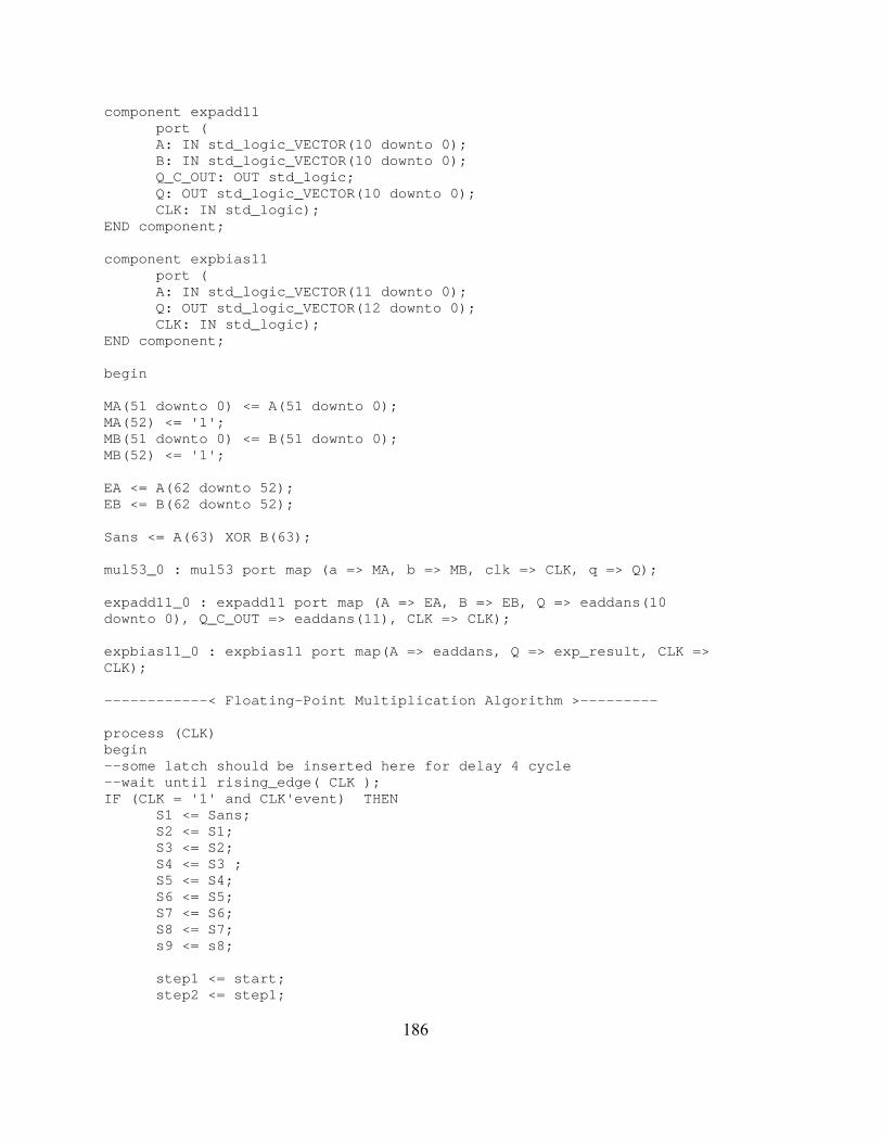
component expadd11 port ( A: IN std_logic_VECTOR(10 downto 0); B: IN std_logic_VECTOR(10 downto 0); Q_C_OUT: OUT std_logic; Q: OUT std_logic_VECTOR(10 downto 0); CLK: IN std_logic); END component; component expbias11 port ( A: IN std_logic_VECTOR(11 downto 0); Q: OUT std_logic_VECTOR(12 downto 0); CLK: IN std_logic); END component; begin MA(51 downto 0) <= A(51 downto 0); MA(52) <= '1'; MB(51 downto 0) <= B(51 downto 0); MB(52) <= '1'; EA <= A(62 downto 52); EB <= B(62 downto 52); Sans <= A(63) XOR B(63); mul53_0 : mul53 port map (a => MA, b => MB, clk => CLK, q => Q); expadd11_0 : expadd11 port map (A => EA, B => EB, Q => eaddans(10 downto 0), Q_C_OUT => eaddans(11), CLK => CLK); expbias11_0 : expbias11 port map(A => eaddans, Q => exp_result, CLK => CLK); ------------< Floating-Point Multiplication Algorithm >--------- process (CLK) begin --some latch should be inserted here for delay 4 cycle --wait until rising_edge( CLK ); IF (CLK = '1' and CLK'event) THEN S1 <= Sans; S2 <= S1; S3 <= S2; S4 <= S3 ; S5 <= S4; S6 <= S5; S7 <= S6; S8 <= S7; s9 <= s8; step1 <= start; step2 <= step1;
186
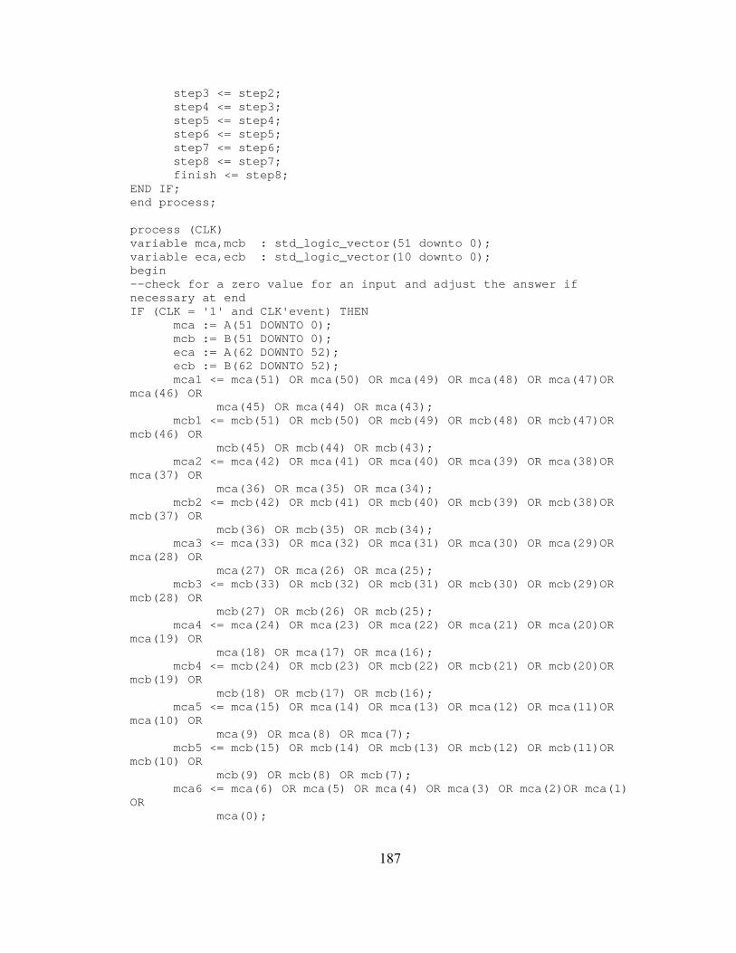
step3 <= step2; step4 <= step3; step5 <= step4; step6 <= step5; step7 <= step6; step8 <= step7; finish <= step8; END IF; end process; process (CLK) variable mca,mcb : std_logic_vector(51 downto 0); variable eca,ecb : std_logic_vector(10 downto 0); begin --check for a zero value for an input and adjust the answer if necessary at end IF (CLK = '1' and CLK'event) THEN mca := A(51 DOWNTO 0); mcb := B(51 DOWNTO 0); eca := A(62 DOWNTO 52); ecb := B(62 DOWNTO 52); mca1 <= mca(51) OR mca(50) OR mca(49) OR mca(48) OR mca(47)OR mca(46) OR mca(45) OR mca(44) OR mca(43); mcb1 <= mcb(51) OR mcb(50) OR mcb(49) OR mcb(48) OR mcb(47)OR mcb(46) OR mcb(45) OR mcb(44) OR mcb(43); mca2 <= mca(42) OR mca(41) OR mca(40) OR mca(39) OR mca(38)OR mca(37) OR mca(36) OR mca(35) OR mca(34); mcb2 <= mcb(42) OR mcb(41) OR mcb(40) OR mcb(39) OR mcb(38)OR mcb(37) OR mcb(36) OR mcb(35) OR mcb(34); mca3 <= mca(33) OR mca(32) OR mca(31) OR mca(30) OR mca(29)OR mca(28) OR mca(27) OR mca(26) OR mca(25); mcb3 <= mcb(33) OR mcb(32) OR mcb(31) OR mcb(30) OR mcb(29)OR mcb(28) OR mcb(27) OR mcb(26) OR mcb(25); mca4 <= mca(24) OR mca(23) OR mca(22) OR mca(21) OR mca(20)OR mca(19) OR mca(18) OR mca(17) OR mca(16); mcb4 <= mcb(24) OR mcb(23) OR mcb(22) OR mcb(21) OR mcb(20)OR mcb(19) OR mcb(18) OR mcb(17) OR mcb(16); mca5 <= mca(15) OR mca(14) OR mca(13) OR mca(12) OR mca(11)OR mca(10) OR mca(9) OR mca(8) OR mca(7); mcb5 <= mcb(15) OR mcb(14) OR mcb(13) OR mcb(12) OR mcb(11)OR mcb(10) OR mcb(9) OR mcb(8) OR mcb(7); mca6 <= mca(6) OR mca(5) OR mca(4) OR mca(3) OR mca(2)OR mca(1) OR mca(0);
187
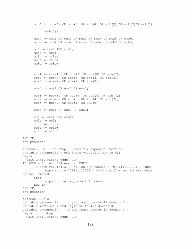
mcb6 <= mcb(6) OR mcb(5) OR mcb(4) OR mcb(3) OR mcb(2)OR mcb(1) OR mcb(0); mca7 <= mca1 OR mca2 OR mca3 OR mca4 OR mca5 OR mca6; mcb7 <= mcb1 OR mcb2 OR mcb3 OR mcb4 OR mcb5 OR mcb6; mc8 <= mca7 AND mcb7; mc8a <= mc8; mc8b <= mc8a; mc8c <= mc8b; mc8d <= mc8c; eca1 <= eca(10) OR eca(9) OR eca(8) OR eca(7); eca2 <= eca(6) OR eca(5) OR eca(4) OR eca(3); eca3 <= eca(2) OR eca(1) OR eca(0); eca4 <= eca1 OR eca2 OR eca3; ecb1 <= ecb(10) OR ecb(9) OR ecb(8) OR ecb(7); ecb2 <= ecb(6) OR ecb(5) OR ecb(4) OR ecb(3); ecb3 <= ecb(2) OR ecb(1) OR ecb(0); ecb4 <= ecb1 OR ecb2 OR ecb3; ec5 <= eca4 AND ecb4; ec5a <= ec5; ec5b <= ec5a; ec5c <= ec5b; ec5d <= ec5c; END IF; end process; process (CLK)--7th step-- Check for exponent overflow variable exponent1a : std_logic_vector(12 downto 0); begin --wait until rising_edge( CLK ); IF (CLK = '1' and CLK'event) THEN IF (exp_result(12) = '1' OR exp_result = "0111111111111") THEN exponent <= "11111111111"; --If overflow set to max value of 254 (biased) ELSE exponent <= exp_result(10 downto 0); END IF; END IF; end process; process (CLK,Q) variable exponent1a : std_logic_vector(11 downto 0); variable mantissa : std_logic_vector(53 downto 0); variable exponent1x : std_logic_vector(10 downto 0); begin --8th step-- --wait until rising_edge( CLK );
188
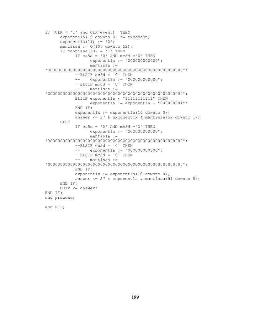
IF (CLK = '1' and CLK'event) THEN exponent1a(10 downto 0) := exponent; exponent1a(11) := '0'; mantissa := Q(105 downto 52); IF mantissa(53) = '1' THEN IF ec5d = '0' AND mc8d ='0' THEN exponent1a := "000000000000"; mantissa := "000000000000000000000000000000000000000000000000000000"; --ELSIF ec5d = '0' THEN -- exponent1a := "000000000000"; --ELSIF mc8d = '0' THEN -- mantissa := "000000000000000000000000000000000000000000000000000000"; ELSIF exponent1a < "11111111111" THEN exponent1a := exponent1a + "000000001"; END IF; exponent1x := exponent1a(10 downto 0); answer <= S7 & exponent1x & mantissa(52 downto 1); ELSE IF ec5d = '0' AND mc8d ='0' THEN exponent1a := "000000000000"; mantissa := "000000000000000000000000000000000000000000000000000000"; --ELSIF ec5d = '0' THEN -- exponent1a := "000000000000"; --ELSIF mc8d = '0' THEN -- mantissa := "000000000000000000000000000000000000000000000000000000"; END IF; exponent1x := exponent1a(10 downto 0); answer <= S7 & exponent1x & mantissa(51 downto 0); END IF; OUTx <= answer; END IF; end process; end RTL;
189

Appendix H – DPFPAdd.vhd
190
-- Double Precision Floating Point Adder -- < dpfpadd.vhd > -- 4/18/2004 -- [email protected] --Author: Kirk A Baugher LIBRARY IEEE; USE IEEE.std_logic_1164.ALL; USE IEEE.std_logic_arith.ALL; USE IEEE.std_logic_unsigned.all; ENTITY dpfpadd IS PORT( CLK :IN STD_LOGIC; start :IN STD_LOGIC; Ain : IN STD_LOGIC_VECTOR(63 DOWNTO 0); Bin : IN STD_LOGIC_VECTOR(63 DOWNTO 0); OUTx : OUT STD_LOGIC_VECTOR(63 DOWNTO 0); finish :OUT STD_LOGIC); END dpfpadd; ARCHITECTURE behavior OF dpfpadd IS SIGNAL ediff1,ediff2,ediffout,Aout,Bout : STD_LOGIC_VECTOR(11 DOWNTO 0); SIGNAL expa,expb,exp1out,exp1out1,exp1out1a,exp1out1b: STD_LOGIC_VECTOR(10 DOWNTO 0); SIGNAL manta,mantb,mantx1out,mant1out,mantx2out,mant1out1 : STD_LOGIC_VECTOR(53 DOWNTO 0); SIGNAL mantx2a,mant1out1a,mant1out1b : STD_LOGIC_VECTOR(53 DOWNTO 0); SIGNAL sa,sb,Sans1out,Sans1out1 : STD_LOGIC; SIGNAL Sans1out1a,Sanswer1,Sans1out1b,Sanswerz1,change : STD_LOGIC; SIGNAL mant_result : STD_LOGIC_VECTOR(53 DOWNTO 0); SIGNAL Sans2,Sans3,Sans4,Sans5,Sans6 : STD_LOGIC; SIGNAL exp1a,exp1b,exp1c,exp1d,exp1e : STD_LOGIC_VECTOR(10 DOWNTO 0); SIGNAL Z1,Z2,Z3,Z4,Z5,Z6,Z7,Z8,Z9,Z10,Z11,zeroflag1,zeroflag2 : std_logic; SIGNAL f1,f2,f3,f4,f5,f6,f7,f8,f9,f10,f11,f12 : STD_LOGIC; SIGNAL SSx1,SSx2,SSx3,SSx4,SSx5,SSx6,SSx7,SSx8,SSxout,SSxout2 : STD_LOGIC; SIGNAL SSout,SStoCompl : STD_LOGIC; SIGNAL expanswer1,expanswerz1 : STD_LOGIC_VECTOR(10 DOWNTO 0); SIGNAL shift1,shiftout,shift,shift12,shiftn2 : STD_LOGIC_VECTOR(5 DOWNTO 0); SIGNAL mantans3,mantz1 : STD_LOGIC_VECTOR(51 DOWNTO 0); SIGNAL mantx2tomantadd : STD_LOGIC_VECTOR(54 DOWNTO 0);
191

--Port A is input, Port B output COMPONENT subexp1 port ( CLK: IN std_logic; A: IN std_logic_VECTOR(11 downto 0); B: IN std_logic_VECTOR(11 downto 0); Q: OUT std_logic_VECTOR(11 downto 0)); END COMPONENT; --Port A is input, Port B output COMPONENT mantadd5 port ( CLK: IN std_logic; A: IN std_logic_VECTOR(53 downto 0); B: IN std_logic_VECTOR(53 downto 0); Q: OUT std_logic_VECTOR(53 downto 0)); END COMPONENT; --Port A is input, Port B output COMPONENT twoscompl port ( CLK: IN std_logic; BYPASS: IN std_logic; A: IN std_logic_VECTOR(53 downto 0); Q: OUT std_logic_VECTOR(54 downto 0)); END COMPONENT; BEGIN Aout <= '0' & Ain(62 DOWNTO 52); Bout <= '0' & Bin(62 DOWNTO 52); subexp12 : subexp1 port map ( A=>Aout, B=>Bout, Q=>ediff1, CLK=>CLK); subexp21 : subexp1 port map ( A=>Bout, B=>Aout, Q=>ediff2, CLK=>CLK); mantexe : mantadd5 port map ( A=>mant1out1a, B=>mantx2out, Q=>mant_result, CLK=>CLK); twos : twoscompl port map ( A=>mantx2a, BYPASS=>SStoCompl, Q=>mantx2tomantadd, CLK=>CLK); PROC1: PROCESS (CLK) --Occurs during expdiff
192
BEGIN IF CLK'EVENT AND CLK='1' THEN expa <= Ain(62 downto 52); manta <= "01" & Ain(51 downto 0); sa <= Ain(63); expb <= Bin(62 downto 52); mantb <= "01" & Bin(51 downto 0); sb <= Bin(63); END IF; END PROCESS PROC1; PROC2: PROCESS (CLK) --depending on expdiff larger number goes to FP1 variable exp1, exp2 : std_logic_vector(10 downto 0); variable mant1, mant2, mantx1 : std_logic_vector(53 downto 0); variable ediff : std_logic_vector(11 downto 0); variable Sans1,SS : std_logic; BEGIN IF CLK'EVENT AND CLK='1' THEN IF ediff1(11) = '0' THEN exp1 := expa; mant1 := manta; Sans1 := sa; exp2 := expb; mant2 := mantb; ediff := ediff1; ELSE exp1 := expb; mant1 := mantb; Sans1 := sb; exp2 := expa; mant2 := manta; ediff := ediff2; END IF; SS := sa XOR sb; --Begin shifting lower number mantissa --IF (ediff(7) OR ediff(6) OR ediff(5)) = '1' THEN--for single-precision IF (ediff(11) OR ediff(10) OR ediff(9) OR ediff(8) OR ediff(7) OR ediff(6)) = '1' THEN --for DP mantx1 := "000000000000000000000000000000000000000000000000000000";--change to 25 zeros for sp ELSE IF ediff(5) = '1' THEN --shift 32 zeros mantx1(20 downto 0) := mant2(52 downto 32); mantx1(52 downto 21) := "00000000000000000000000000000000"; ELSE --For Single Precision
193
--IF ediff(4) = '1' THEN--shift 16 zeros -- mantx1(36 downto 0) := mant2(52 downto 16); -- mantx1(52 downto &d) := "0000000000000000"; -- mantx1(37 downto &d) := "0000000000000000"; --ELSE mantx1 := mant2; END IF; END IF; SSout <= SS; mantx1out <= mantx1; exp1out <= exp1; mant1out <= mant1; Sans1out <= Sans1; ediffout <= ediff; END IF; END PROCESS PROC2; PROC3: PROCESS (CLK) --Finish shifting variable mantx2 : std_logic_vector(53 downto 0); variable ediffa : std_logic_vector(11 downto 0); variable SSx : std_logic; BEGIN IF CLK'EVENT AND CLK='1' THEN SSx := SSout; mantx2 := mantx1out; ediffa := ediffout; --Comment ediffa(4) out for single precision IF ediffa(4) = '1' THEN--shift 16 zeros mantx2(36 downto 0) := mantx2(52 downto 16); mantx2(52 downto 37) := "0000000000000000"; ELSE mantx2 := mantx2; END IF; IF ediffa(3)='1' THEN--shift 8 zeros mantx2(44 downto 0) := mantx2(52 downto 8); mantx2(52 downto 45) := "00000000"; ELSE mantx2 := mantx2; END IF; IF ediffa(2)='1' THEN--shift 4 zeros mantx2(48 downto 0) := mantx2(52 downto 4); mantx2(52 downto 49) := "0000"; ELSE mantx2 := mantx2; END IF; IF ediffa(1)='1' THEN--shift 2 zeros mantx2(50 downto 0) := mantx2(52 downto 2); mantx2(52 downto 51) := "00";
194
ELSE mantx2 := mantx2; END IF; IF ediffa(0)='1' THEN--shift 1 zeros mantx2(51 downto 0) := mantx2(52 downto 1); mantx2(52) := '0'; ELSE mantx2 := mantx2; END IF; -- IF SSx = '1' THEN -- mantx2 := NOT(mantx2) + 1; -- ELSE -- mantx2 := mantx2; -- END IF; mantx2a <= mantx2; exp1out1 <= exp1out; mant1out1 <= mant1out; Sans1out1 <= Sans1out; SSxout <= SSx; SStoCompl <= NOT(SSx); END IF; END PROCESS PROC3; --this process occurs during the twos compliment PROC2_3: PROCESS (CLK) BEGIN IF CLK'EVENT AND CLK='1' THEN mantx2out<=mantx2tomantadd(53 DOWNTO 0); SSxout2<=SSxout; exp1out1b <= exp1out1; exp1out1a <= exp1out1b; mant1out1b <= mant1out1; mant1out1a <= mant1out1b; Sans1out1b <= Sans1out1; Sans1out1a <= Sans1out1b; END IF; END PROCESS PROC2_3; PROC4: PROCESS (CLK) --mantissa normalization variable mant_result1 : std_logic_vector(53 downto 0); variable mantans1 : std_logic_vector(51 downto 0); variable expanswer : std_logic_vector(10 downto 0); variable Sanswer : std_logic; --variable shift : std_logic_vector(5 downto 0); BEGIN IF CLK'EVENT AND CLK='1' THEN mant_result1 := mant_result; expanswer := exp1e; Sanswer := Sans6;
195
change <= '1'; IF mant_result1(53) = '1' THEN mantans1 := mant_result1(52 downto 1); shift <= "000000"; --shiftn <= "000001"; shiftn2 <= "000001"; ELSIF mant_result1(52) = '1' THEN mantans1 := mant_result1(51 downto 0); shift <= "000000"; --shiftn <= "000010"; shiftn2 <= "000000"; ELSIF mant_result1(51) = '1' THEN mantans1(51 downto 1) := mant_result1(50 downto 0); mantans1(0) := '0'; shift <= "000001"; --shiftn <= "000011"; shiftn2 <= "000001"; ELSIF mant_result1(50) = '1' THEN shift <= "000010"; --shiftn <= "000100"; shiftn2 <= "000010"; mantans1(51 downto 2) := mant_result1(49 downto 0); mantans1(1 downto 0) := "00"; ELSIF mant_result1(49) = '1' THEN shift <= "000011"; --shiftn <= "000101"; shiftn2 <= "000011"; mantans1(51 downto 3) := mant_result1(48 downto 0); mantans1(2 downto 0) := "000"; ELSIF mant_result1(48) = '1' THEN shift <= "000100"; --shiftn <= "000110"; shiftn2 <= "000100"; mantans1(51 downto 4) := mant_result1(47 downto 0); mantans1(3 downto 0) := "0000"; ELSIF mant_result1(47) = '1' THEN shift <= "000101"; --shiftn <= "000111"; shiftn2 <= "000101"; mantans1(51 downto 5) := mant_result1(46 downto 0); mantans1(4 downto 0) := "00000"; ELSIF mant_result1(46) = '1' THEN shift <= "000110"; --shiftn <= "001000"; shiftn2 <= "000110"; mantans1(51 downto 6) := mant_result1(45 downto 0); mantans1(5 downto 0) := "000000"; ELSIF mant_result1(45) = '1' THEN shift <= "000111"; --shiftn <= "001001"; shiftn2 <= "000111"; mantans1(51 downto 7) := mant_result1(44 downto 0); mantans1(6 downto 0) := "0000000"; ELSIF mant_result1(44) = '1' THEN shift <= "001000";
196
--shiftn <= "001010"; shiftn2 <= "001000"; mantans1(51 downto 8) := mant_result1(43 downto 0); mantans1(7 downto 0) := "00000000"; ELSIF mant_result1(43) = '1' THEN shift <= "001001"; --shiftn <= "001011"; shiftn2 <= "001001"; mantans1(51 downto 9) := mant_result1(42 downto 0); mantans1(8 downto 0) := "000000000"; ELSIF mant_result1(42) = '1' THEN shift <= "001010"; --shiftn <= "001100"; shiftn2 <= "001010"; mantans1(51 downto 10) := mant_result1(41 downto 0); mantans1(9 downto 0) := "0000000000"; ELSIF mant_result1(41) = '1' THEN shift <= "001011"; --shiftn <= "001101"; shiftn2 <= "001011"; mantans1(51 downto 11) := mant_result1(40 downto 0); mantans1(10 downto 0) := "00000000000"; ELSIF mant_result1(40) = '1' THEN shift <= "001100"; --shiftn <= "001110"; shiftn2 <= "001100"; mantans1(51 downto 12) := mant_result1(39 downto 0); mantans1(11 downto 0) := "000000000000"; ELSIF mant_result1(39) = '1' THEN shift <= "001101"; --shiftn <= "001111"; shiftn2 <= "001101"; mantans1(51 downto 13) := mant_result1(38 downto 0); mantans1(12 downto 0) := "0000000000000"; ELSIF mant_result1(38) = '1' THEN shift <= "001110"; --shiftn <= "010000"; shiftn2 <= "001110"; mantans1(51 downto 14) := mant_result1(37 downto 0); mantans1(13 downto 0) := "00000000000000"; ELSIF mant_result1(37) = '1' THEN shift <= "001111"; --shiftn <= "010001"; shiftn2 <= "001111"; mantans1(51 downto 15) := mant_result1(36 downto 0); mantans1(14 downto 0) := "000000000000000"; ELSIF mant_result1(36) = '1' THEN shift <= "010000"; --shiftn <= "010010"; shiftn2 <= "010000"; mantans1(51 downto 16) := mant_result1(35 downto 0); mantans1(15 downto 0) := "0000000000000000"; ELSIF mant_result1(35) = '1' THEN shift <= "010001"; --shiftn <= "010011";
197

shiftn2 <= "010001"; mantans1(51 downto 17) := mant_result1(34 downto 0); mantans1(16 downto 0) := "00000000000000000"; ELSIF mant_result1(34) = '1' THEN shift <= "010010"; --shiftn <= "010100"; shiftn2 <= "010010"; mantans1(51 downto 18) := mant_result1(33 downto 0); mantans1(17 downto 0) := "000000000000000000"; ELSIF mant_result1(33) = '1' THEN shift <= "010011"; --shiftn <= "010101"; shiftn2 <= "010011"; mantans1(51 downto 19) := mant_result1(32 downto 0); mantans1(18 downto 0) := "0000000000000000000"; ELSIF mant_result1(32) = '1' THEN shift <= "010100"; --shiftn <= "010110"; shiftn2 <= "010100"; mantans1(51 downto 20) := mant_result1(31 downto 0); mantans1(19 downto 0) := "00000000000000000000"; ELSIF mant_result1(31) = '1' THEN shift <= "010101"; --shiftn <= "010111"; shiftn2 <= "010101"; mantans1(51 downto 21) := mant_result1(30 downto 0); mantans1(20 downto 0) := "000000000000000000000"; ELSIF mant_result1(30) = '1' THEN shift <= "010110"; --shiftn <= "011000"; shiftn2 <= "010110"; mantans1(51 downto 22) := mant_result1(29 downto 0); mantans1(21 downto 0) := "0000000000000000000000"; ELSIF mant_result1(29) = '1' THEN shift <= "010111"; --shiftn <= "011001"; shiftn2 <= "010111"; mantans1(51 downto 23) := mant_result1(28 downto 0); mantans1(22 downto 0) := "00000000000000000000000"; ELSIF mant_result1(28) = '1' THEN shift <= "011000"; --shiftn <= "011010"; shiftn2 <= "011000"; mantans1(51 downto 24) := mant_result1(27 downto 0); mantans1(23 downto 0) := "000000000000000000000000"; ELSE mantans1 := mant_result1(51 DOWNTO 0); change<='0'; shift <= "000000"; --shiftn <= "000000"; shiftn2 <= "000000"; END IF; mantz1 <= mantans1; shiftout <=shift; expanswerz1<=expanswer;
198

Sanswerz1<=Sanswer; END IF; END PROCESS PROC4; PROC4A: PROCESS (CLK) --mantissa normalization variable mant_result1a : std_logic_vector(51 downto 0);--was 53 variable mantans : std_logic_vector(51 downto 0); variable expanswer : std_logic_vector(10 downto 0); variable Sanswer : std_logic; variable shiftc,shiftd2 : std_logic_vector(5 downto 0); BEGIN IF CLK'EVENT AND CLK='1' THEN --shiftc := shiftout; shiftc := shift; --shiftd := shiftn; shiftd2 := shiftn2; mant_result1a := mantz1; expanswer := expanswerz1; Sanswer := Sanswerz1; IF change = '1' THEN mantans := mant_result1a; ELSIF mant_result1a(27) = '1' THEN shiftc := "011001"; --shiftd := "011011"; shiftd2 := "011001"; mantans(51 downto 25) := mant_result1a(26 downto 0); mantans(24 downto 0) := "0000000000000000000000000"; ELSIF mant_result1a(26) = '1' THEN shiftc := "011010"; --shiftd := "011100"; shiftd2 := "011010"; mantans(51 downto 26) := mant_result1a(25 downto 0); mantans(25 downto 0) := "00000000000000000000000000"; ELSIF mant_result1a(25) = '1' THEN shiftc := "011011"; --shiftd := "011101"; shiftd2 := "011011"; mantans(51 downto 27) := mant_result1a(24 downto 0); mantans(26 downto 0) := "000000000000000000000000000"; ELSIF mant_result1a(24) = '1' THEN shiftc := "011100"; --shiftd := "011110"; shiftd2 := "011100"; mantans(51 downto 28) := mant_result1a(23 downto 0); mantans(27 downto 0) := "0000000000000000000000000000"; ELSIF mant_result1a(23) = '1' THEN shiftc := "011101"; --shiftd := "011111"; shiftd2 := "011101"; mantans(51 downto 29) := mant_result1a(22 downto 0); mantans(28 downto 0) := "00000000000000000000000000000"; ELSIF mant_result1a(22) = '1' THEN shiftc := "011110"; --shiftd := "100000";
199
shiftd2 := "011110"; mantans(51 downto 30) := mant_result1a(21 downto 0); mantans(29 downto 0) := "000000000000000000000000000000"; ELSIF mant_result1a(21) = '1' THEN shiftc := "011111"; --shiftd := "100001"; shiftd2 := "011111"; mantans(51 downto 31) := mant_result1a(20 downto 0); mantans(30 downto 0) := "0000000000000000000000000000000"; ELSIF mant_result1a(20) = '1' THEN shiftc := "100000"; --shiftd := "100010"; shiftd2 := "100000"; mantans(51 downto 32) := mant_result1a(19 downto 0); mantans(31 downto 0) := "00000000000000000000000000000000"; ELSIF mant_result1a(19) = '1' THEN shiftc := "100001"; --shiftd := "100011"; shiftd2 := "100001"; mantans(51 downto 33) := mant_result1a(18 downto 0); mantans(32 downto 0) := "000000000000000000000000000000000"; ELSIF mant_result1a(18) = '1' THEN shiftc := "100010"; --shiftd := "100100"; shiftd2 := "100010"; mantans(51 downto 34) := mant_result1a(17 downto 0); mantans(33 downto 0) := "0000000000000000000000000000000000"; ELSIF mant_result1a(17) = '1' THEN shiftc := "100011"; --shiftd := "100101"; shiftd2 := "100011"; mantans(51 downto 35) := mant_result1a(16 downto 0); mantans(34 downto 0) := "00000000000000000000000000000000000"; ELSIF mant_result1a(16) = '1' THEN shiftc := "100100"; --shiftd := "100110"; shiftd2 := "100100"; mantans(51 downto 36) := mant_result1a(15 downto 0); mantans(35 downto 0) := "000000000000000000000000000000000000"; ELSIF mant_result1a(15) = '1' THEN shiftc := "100101"; --shiftd := "100111"; shiftd2 := "100101"; mantans(51 downto 37) := mant_result1a(14 downto 0); mantans(36 downto 0) := "0000000000000000000000000000000000000"; ELSIF mant_result1a(14) = '1' THEN shiftc := "100110"; --shiftd := "101000"; shiftd2 := "100110"; mantans(51 downto 38) := mant_result1a(13 downto 0);
200
mantans(37 downto 0) := "00000000000000000000000000000000000000"; ELSIF mant_result1a(13) = '1' THEN shiftc := "100111"; --shiftd := "101001"; shiftd2 := "100111"; mantans(51 downto 39) := mant_result1a(12 downto 0); mantans(38 downto 0) := "000000000000000000000000000000000000000"; ELSIF mant_result1a(12) = '1' THEN shiftc := "101000"; --shiftd := "101010"; shiftd2 := "101000"; mantans(51 downto 40) := mant_result1a(11 downto 0); mantans(39 downto 0) := "0000000000000000000000000000000000000000"; ELSIF mant_result1a(11) = '1' THEN shiftc := "101001"; --shiftd := "101011"; shiftd2 := "101001"; mantans(51 downto 41) := mant_result1a(10 downto 0); mantans(40 downto 0) := "00000000000000000000000000000000000000000"; ELSIF mant_result1a(10) = '1' THEN shiftc := "101010"; --shiftd := "101100"; shiftd2 := "101010"; mantans(51 downto 42) := mant_result1a(9 downto 0); mantans(41 downto 0) := "000000000000000000000000000000000000000000"; ELSIF mant_result1a(9) = '1' THEN shiftc := "101011"; --shiftd := "101101"; shiftd2 := "101011"; mantans(51 downto 43) := mant_result1a(8 downto 0); mantans(42 downto 0) := "0000000000000000000000000000000000000000000"; ELSIF mant_result1a(8) = '1' THEN shiftc := "101100"; --shiftd := "101110"; shiftd2 := "101100"; mantans(51 downto 44) := mant_result1a(7 downto 0); mantans(43 downto 0) := "00000000000000000000000000000000000000000000"; ELSIF mant_result1a(7) = '1' THEN shiftc := "101101"; --shiftd := "101111"; shiftd2 := "101101"; mantans(51 downto 45) := mant_result1a(6 downto 0); mantans(44 downto 0) := "000000000000000000000000000000000000000000000"; ELSIF mant_result1a(6) = '1' THEN shiftc := "101110"; --shiftd := "110000"; shiftd2 := "101110";
201
mantans(51 downto 46) := mant_result1a(5 downto 0); mantans(45 downto 0) := "0000000000000000000000000000000000000000000000"; ELSIF mant_result1a(5) = '1' THEN shiftc := "101111"; --shiftd := "110001"; shiftd2 := "101111"; mantans(51 downto 47) := mant_result1a(4 downto 0); mantans(46 downto 0) := "00000000000000000000000000000000000000000000000"; ELSIF mant_result1a(4) = '1' THEN shiftc := "110000"; --shiftd := "110010"; shiftd2 := "110000"; mantans(51 downto 48) := mant_result1a(3 downto 0); mantans(47 downto 0) := "000000000000000000000000000000000000000000000000"; ELSIF mant_result1a(3) = '1' THEN shiftc := "110001"; --shiftd := "110011"; shiftd2 := "110001"; mantans(51 downto 49) := mant_result1a(2 downto 0); mantans(48 downto 0) := "0000000000000000000000000000000000000000000000000"; ELSIF mant_result1a(2) = '1' THEN shiftc := "110010"; --shiftd := "110100"; shiftd2 := "110010"; mantans(51 downto 50) := mant_result1a(1 downto 0); mantans(49 downto 0) := "00000000000000000000000000000000000000000000000000"; ELSIF mant_result1a(1) = '1' THEN shiftc := "110011"; shiftd2 := "110011"; --shiftd := "110101"; mantans(51) := mant_result1a(0); mantans(50 downto 0) := "000000000000000000000000000000000000000000000000000"; ELSE shiftc := "000000"; --shiftd := "000000"; shiftd2 := "000000"; mantans := "0000000000000000000000000000000000000000000000000000"; END IF; -- OUTx <= Sanswer & expanswer & mantans; Sanswer1 <= Sanswer; expanswer1 <= expanswer; mantans3 <= mantans; shift1 <= shiftc; --shift11 <= shiftd; shift12 <= shiftd2; END IF; END PROCESS PROC4A;
202
PROC4_B: PROCESS (CLK)--occurs during normalization BEGIN IF CLK'EVENT AND CLK='1' THEN Sans2 <= Sans1out1a; Sans3 <= Sans2; Sans4 <= Sans3; Sans5 <= Sans4; Sans6 <= Sans5; SSx1 <= SSxout2; SSx2 <= SSx1; SSx3 <= SSx2; SSx4 <= SSx3; SSx5 <= SSx4; SSx6 <= SSx5; SSx7 <= SSx6; SSx8 <= SSx7; exp1a <= exp1out1a; exp1b <= exp1a; exp1c <= exp1b; exp1d <= exp1c; exp1e <= exp1d; END IF; END PROCESS PROC4_B; PROCESS_EXP_ADJ: PROCESS (CLK) variable expanswer2 : STD_LOGIC_VECTOR(10 DOWNTO 0); variable mantans4 : STD_LOGIC_VECTOR(51 DOWNTO 0); variable Sanswer2 : STD_LOGIC; variable shift1x,shift12x : STD_LOGIC_VECTOR(5 DOWNTO 0); BEGIN IF CLK'EVENT AND CLK='1' THEN Sanswer2 := Sanswer1; expanswer2 := expanswer1; mantans4 := mantans3; shift1x := shift1; --shift11x := shift11; shift12x := shift12; IF Z11 = '1' THEN Sanswer2 := '0'; expanswer2 := (OTHERS=>'0'); mantans4 := (OTHERS=>'0'); ELSIF (shift1x > "000000" AND SSx8 = '1') THEN expanswer2 := expanswer2 - shift1x; ELSIF (shift12x > "000000" AND SSx8 = '0') THEN expanswer2 := expanswer2 + shift12x; END IF; OUTx <= Sanswer2 & expanswer2 & mantans4;
203
END IF; END PROCESS PROCESS_EXP_ADJ; PROCESS_FINISH: PROCESS (CLK) BEGIN IF CLK'EVENT AND CLK='1' THEN f1 <= start; f2 <= f1; f3 <= f2; f4 <= f3; f5 <= f4; f6 <= f5; f7 <= f6; f8 <= f7; f9 <= f8; f10 <= f9; f11 <= f10; f12 <= f11; finish <= f12; END IF; END PROCESS PROCESS_FINISH; Zerocheck1: PROCESS (CLK) BEGIN IF CLK'EVENT AND CLK='1' THEN IF Ain = "0000000000000000000000000000000000000000000000000000000000000000" THEN zeroflag1 <= '1'; ELSE zeroflag1 <= '0'; END IF; END IF; END PROCESS Zerocheck1; Zerocheck2: PROCESS (CLK) BEGIN IF CLK'EVENT AND CLK='1' THEN IF Bin = "0000000000000000000000000000000000000000000000000000000000000000" THEN zeroflag2 <= '1'; ELSE zeroflag2 <= '0'; END IF; END IF; END PROCESS Zerocheck2; Zeropass: PROCESS (CLK) BEGIN IF CLK'EVENT AND CLK='1' THEN Z1 <= zeroflag1 AND zeroflag2; Z2 <= Z1; Z3 <= Z2; Z4 <= Z3;
204
Z5 <= Z4; Z6 <= Z5; Z7 <= Z6; Z8 <= Z7; Z9 <= Z8; Z10 <= Z9; Z11 <= Z10; END IF; END PROCESS Zeropass; END behavior;
205

Vita
Kirk Andrew Baugher was born on January 2, 1980 in Enterprise, Alabama. Kirk
was raised in all across the country spending his childhood and adolescent life in
Alabama, Washington, Virginia, Tennessee, and Texas. He began attending college at
the University of Tennessee, Knoxville in the fall of 1998. During his undergraduate
term at the University of Tennessee, Kirk co-oped for one year with the Tennessee Valley
Authority and soon graduated with a Bachelor of Science degree in Computer
Engineering and a minor in Engineering Communication and Performance in 2003.
Immediately following the completion of his undergraduate degree, Kirk started his
graduate degree. One year later in 2004, Kirk graduated with a Master of Science in
Electrical Engineering.
Kirk will be starting his career as an engineer with Honeywell in Clearwater,
Florida.
206