spatially controllable chemical vapor depositionfigs.pdf · spatially controllable chemical vapor...
TRANSCRIPT

Spatially controllable chemical vapor deposition
Jae-Ouk Choo and Raymond A. Adomaitis1
Department of Chemical Engineering
and Institute for Systems Research
University of Maryland
College Park, MD 20742
Gary W. Rubloff, Laurent Henn-Lecordier, and Yijun Liu2
Department of Materials Science and Engineering
and Institute for Systems Research
University of Maryland
College Park, MD 20742
December 2, 2003
Abstract
Most conventional chemical vapor deposition (CVD) systems do not have the spatial actuationand sensing capabilities necessary to control deposition uniformity, or to intentionally induce nonuni-form deposition patterns for single-wafer combinatorial CVD experiments. In an effort to addressthis limitation, a novel CVD reactor system has been developed that can explicitly control the spa-tial profile of gas-phase chemical composition across the wafer surface. This paper discusses thesimulation-based design of a prototype reactor system and the results of preliminary experimentsperformed to evaluate the performance of the prototype in depositing tungsten films. Initial exper-imental results demonstrate that it is possible to produce spatially patterned wafers using a CVDprocess by controlling gas phase reactant composition.
Topical heading: Process Systems Engineering
Keywords: Semiconductor processing; Chemical vapor deposition; Distributed parameter systems;Simulation.
1Corresponding author. Email: [email protected] address: ASM International, 3440 East University Drive Phoenix, AZ 85034-7200.
1

2
1 Introduction
Chemical Vapor Deposition (CVD) is one of the essential unit operations in semiconductor manufac-
turing because of its ability to deposit thin smooth films conformally onto submicron-scale features.
CVD processes have evolved together with the semiconductor industry, from early bell-jar CVD re-
actors to the current cold-wall single-wafer reactor (Xia et al. 2000). The continuing reduction of
device feature size, growing scale of device integration, expanding number of new electronic materi-
als, and increasing substrate (wafer) size motivate development of the new CVD processes necessary
to sustain the advancement of microelectronic technology. However, equipment designs are aimed
at specific deposition processes and operating conditions (e.g., pressures, chemical species, flows,
temperatures) with the design goal of producing process uniformity across large wafers (300 mm dia,
resulting in hundreds of semiconductor chips) at the nominal design conditions. Optimizing a design
to CVD and other manufacturing equipment for a specific range of design conditions has a number
of fundamental shortcomings:
1. Semiconductor manufacturing processes change rapidly in time (e.g., relative to typical petro-
chemical processes). Because technology improvements must be implemented incrementally
to maintain or improve yields in complex, multi-step wafer production sequences, a new gen-
eration of process equipment technology may only emerge after several of these improvement
steps.
2. Process conditions for optimal material and device quality often do not meet the across-wafer
uniformity requirements for manufacturing, forcing a tradeoff between product performance
and manufacturing productivity.
3. Fundamental chemical and physical mechanisms for semiconductor processes are often not well
known, so that it is difficult to identify a priori the best design which balances the demands of
product performance and manufacturing uniformity.
4. Experimentation for process optimization is expensive, requiring sets of runs to investigate and
characterize complex process behavior.
1.1 Equipment design for uniformity
Current CVD reactor designs typically consist of a cooled-wall reaction (vacuum) chamber in which
one to several wafers are processed. Energy needed to drive the deposition reactions is provided by an
inductively-heated susceptor or a wafer stage heated by external lamps or internal resistance heating.

3
Reactant gases enter the reaction chamber through a gas delivery system, flow over the wafer(s),
and the residual gas is pumped out through the chamber exhaust port. Because of the importance
of spatially uniform (across-wafer) processing capabilities, showerhead designs for gas delivery to
the wafer typically incorporate a high density of uniformly spaced small holes in an attempt to
distribute gas flow as uniformly as possible across a large diameter wafer. In addition, reactor design
components including chamber, wafer position (and rotation), pumping, heating, and gas inlet are
commonly structured to achieve high uniformity with cylindrical symmetry about the wafer.
Significant research effort has been directed towards improving growth uniformity of CVD pro-
cess. Early experimental and simulation-based process equipment research focused on developing
an understanding of the important transport and reaction mechanisms of CVD processes and de-
vising optimization methods to aid process parameter selection. For example, Wang et al. (1986)
used flow visualization techniques to show that heated wafers can disturb gas flow patterns; their
experiments suggested lowering operation pressures to reduce the perturbation. Moffat and Jensen
(1988) demonstrated the utility of simulation technology for process optimization in the context of
a horizontal Si homoepitaxial deposition reactor. Their simulation study examined the relationship
between the growth uniformity and tilt angle of the susceptor, giving the optimal setting for this
reactor geometry parameter. Another example of rigorous modeling and simulation was performed
by Kleijn et al. (1989). Their mathematical model was used to show the significance of thermal
diffusion and its effect on growth uniformity and gas-phase reactant species distribution.
The evolution of CVD reactor designs also has been motivated by the need to improve growth
uniformity. For example, various showerhead designs have been developed to generate uniform gas
flow patterns over the wafer surface (Gadgil 1993; Wang et al. 1986) or to produce uniform film
deposition rates (Kobayashi et al. 1997; Kim and Lee 1997). Still more advanced design features are
found in the annular, three-zone Texas Instruments showerhead (Moslehi et al. 1995) for tungsten
and other CVD processes, where individual gas mass flow controllers could be used to set the gas
flow rate to each segment.
In some MOCVD processes, the separation of gas precursors is critical because highly reactive
gas precursors can cause undesirable gas phase reactions. In an effort to reduce gas phase reactions,
Van der Stricht et al. (1997) developed a vertical reactor with separate feed ports for each precursor
species, and experiments revealed the relationship between the wafer rotation rate and thickness
uniformity of GaN and InGaN films. Another example of using separate gas injectors for individual
precursors can be found in the horizontal flow MOCVD reactor introduced by Yang et al. (1999).

4
Theodoropoulos et al. (2000) described a new MOCVD reactor design of featuring an annular-ring
showerhead configuration that allowed the controlled injection of separate precursors. Several annual
ring designs were evaluated in this study, and as with Van der Stricht and Yang, Theodoropoulos
and co-workers concluded that novel gas delivery designs offered new operational degrees of freedom
with which uniformity could be controlled; they also pointed to the importance of simulation tools
in selecting optimized operating conditions.
CVD reactor designs have been developed specifically to allow or improve active control of wafer
processing conditions during the dynamic processing cycle. For example, work at TI (Moslehi et
al. 1992) exploited multiple (3 and 4) heating zones radially across the wafer in single-wafer rapid
thermal processing to achieve temperature uniformity. This approach has been incorporated into
commercial RTP equipment, e.g., from CVC Products, Inc., and from Applied Materials. The
SEMATECH testbed RTP system (Stuber et al. 1998) and the three-zone RTP system at North
Carolina State University (Kiether et al. 1994) exploit independent lamp zones for edge-cooling
compensation and dynamic uniformity control. Further developments in this area include reduced-
model-based real-time control studies of the three-zone NCSU RTP system (Theodoropoulou et al.
1999; Christofides 2001) and reduced-model-based order state estimation and optimal control of a
horizontal high-pressure CVD system (Banks et al. 2002; Kepler et al. 2000, 2001).
1.2 The Programmable Reactor concept
The existing design strategy of semiconductor CVD manufacturing equipment faces fundamental
barriers limiting the development of next-generation reactor systems; there is a need for a new design
paradigm to: (1) decouple fundamental materials and product quality requirements from across-wafer
uniformity in manufacturing, so that both may be achieved simultaneously; (2) accelerate materials
and process learning and optimization; and (3) develop equipment that is flexible and scalable to
succeeding generations of the technology.
As a response to these perceived CVD reactor design shortcomings, this paper presents the
development of a novel CVD reactor intended to improve across-wafer 2-dimensional controllability.
This new CVD reactor introduces a segmented showerhead design featuring individually controllable
gas distribution actuators, a design that reverses the residual gas flow by directing it up through
the showerhead, and sampling ports for in-situ gas sampling (Fig. 1). In this paper, we describe
the development of this novel design concept by simulation, a sequence of experiments performed
using a prototype reactor, and the interpretation of preliminary experimental data by simulation to

5
demonstrate the validity of the design principles.
We refer to this design as the Programmable CVD Reactor concept because of the potential
real-time control of gas phase composition across the wafer surface has for making possible novel
operating modes. For example, this reactor design will enable single-wafer combinatorial experiments
in which different materials can be created or different process conditions can be tested in a single
experiment, producing the library wafer illustrated in Fig. 2. In subsequent deposition runs, the
reactor then can be reprogrammed to produce uniform films corresponding to one point on the
library wafer without making any hardware adjustments. This mode of operation is made possible by
the combination of the flexible design of the Programmable Reactor and model-based interpretation
of the sensor and metrology data collected during the processing of the library wafer.
2 Reactor Design Principles
A common feature of all the CVD systems discussed in the previous section having the capability of
controlling spatial variations in gas composition leaving the showerhead (e.g., Moslehi et al. 1995 and
Theodoropoulos et al. 2000) is that the actuation capabilities are limited to 1-dimensional control
in the radial direction. Furthermore, a characteristic common to these designs is the segment-to-
segment interaction produced by the net flow of reactant gas across the wafer to the reactor chamber
exhaust. For example, consider the simulation results presented in Fig. 3, where the total gas flow
from each of the three injection segments of the showerhead are adjusted to produce a nearly uniform
gas velocity field over the wafer radius. If inert gas is injected through the center and outer annular
region, and the deposition precursor species are injected through the middle annular injection port,
it is easy to see that the net convection across the wafer shifts the region where the precursor plume
interacts with the wafer surface downstream relative to the injection point. Therefore, the net flux
across the wafer surface, inherent in the annual segmented showerhead designs, reduces the ability
to accurately control gas phase composition at the wafer surface.
As an alternative to reactor systems based on the annular segmented showerhead design, the
Programmable Reactor system incorporates three new design features to improve the spatial control
of gas phase composition. The first is the development of a showerhead design consisting of an
assembly of hexagonal showerhead sub-elements (segments) arrayed across the wafer surface. The
reactant gas composition and feed rate is controllable within each segment, resulting in true 2-
dimensional control of gas composition across the wafer. The spatial resolution with which gas
phase composition can be controlled is determined by the size of showerhead segments.

6
The second new design feature is the recirculation of residual gas up through each segment of
the showerhead; exhaust gases mix in a common exhaust volume above the showerhead honeycomb
structure (Fig. 1). When the total volumetric flow rate of feed gas to each segment is equal, the
effect of this design feature is to create periodic flow fields in the region between the bottom of the
showerhead assembly and the wafer surface (Fig. 4). This simulation result was produced using the
Fluent CFD package and is based on gas flow rates, compositions, and showerhead segment length
scales comparable to the prototype system that was constructed, and which is described later in this
paper. In this simulation result it is possible to see that the boundaries of the periodic flow field
match the segment wall locations, indicating that there will be no convective flux of reactant species
between the segment regions, eliminating the problems generated by drawing exhaust gas across the
wafer surface.
The elimination of inter-segment region convective transport will improve the accuracy with
which gas composition can be controlled across the wafer surface because across-wafer transport
will be governed solely by diffusion. The third new design feature of the Programmable Reactor
is the ability to manipulate the showerhead/wafer gap size. Small gap settings will reduce inter-
segment diffusion in the gap region leading to deposition of distinct hexagonal patterns; increasing
the gap size will spread the pattern, ultimately producing smooth concentration gradients across
the wafer surface when reactant gas composition varies from segment-to-segment. An example of
the smooth concentration gradients across the wafer surface that can be produced in this manner
is shown in the simulation results depicted in Fig. 5, where the across-wafer concentration profile
of a particular reactant species is shown for a two-segment reactor design. As with the previous
simulation, this simulation result was produced using the Fluent CFD package and is based on gas
flow rates, compositions, and length scales comparable to the prototype system.
Because of the reduced effect the gas velocity field has on the gas concentration profile across
the wafer surface, the accuracy of simulators used to interpret deposition data will be enhanced,
improving the ability to correlate process operating conditions with film properties at all points on
the library wafer. Because of the potential for accurately predicting the continuous variation of gas
phase concentration across the wafer surface, it may be possible to generate library wafers with
continuously graded characteristics across the wafer surface, increasing the information that can be
obtained from a single deposition run. The system then can be run with closer showerhead-wafer
spacing to produce a finite number of hexagonal patches of material selected from the first library
wafer, to provide a more accurate assessment of the process conditions needed to produce the desired

7
material.
2.1 Prototype construction
To test the feasibility of the Programmable CVD concept, a prototype reactor was designed and
constructed by modifying one reaction chamber of an Ulvac-ERA1000 CVD cluster tool (Fig. 6).
The Ulvac cluster tool located on the University of Maryland’s campus is a commercial CVD system
used for selective tungsten (W) deposition. W CVD, used to form vertical interconnects in VLSI
and ULSI circuits, represents a relatively mature, but commercially important, manufacturing process
(Ireland 1997), and so was chosen for evaluating the engineering design of the programmable reactor.
While W CVD deposition mechanisms and reactor systems have been studied extensively (e.g.,
Arora and Pollard 1991; Kleijn 2000; Kleijn et al. 1991; Kleijn and Werner 1993), open process
development issues remain. Even in the simplest case of blanket deposition using H2 and WF6, the
reactant/reducing gas ratio and WF6 gas concentration result in two operational degrees of freedom
that force a tradeoff between film conformality and deposition rate, where the latter is compounded
by reactor design factors that determine where the transition from reaction rate to mass-transfer
limited operation takes place.
In its original configuration, the hydrogen reducing gas entered through a quartz showerhead
above the wafer; wafer heating was provided by a ring of heating lamps above the showerhead.
As part of the Programmable Reactor modifications, substrate heating was used in place of lamp
heating, and the quartz showerhead was replaced by the new Programmable Reactor showerhead
assembly. The primary component of the assembly is the honeycomb-shaped array of three segments
machined from a single block of stainless steel. Each side of the hexagonal segments is W = 1in
in length and the overall length of the honeycomb segment structure is L = 5.67in. As designed,
the three segments cover most of the surface area of the 4in wafers used in deposition experiments.
The segment length was made as long as physically possible subject to the constraints imposed
by clearances necessary to insert the wafer and to prevent obstruction of the exhaust ports in the
showerhead chamber.
Each segment is fitted with two 0.25in ID feed tubes and one sampling tube (Figs. 7 and 8). The
feed and sampling tube vertical positions can be adjusted when the reactor is not operating. The
sampling tube of each segment can be used to transport a small amount of gas to a real time in-situ
sensor, such as a mass spectrometer. From the residual gas analysis of each segment, approximate
film thickness and the composition of film deposited on each area corresponding to each segment

8
can be determined (Gougousi et al. 2000).
Individual mass flow controllers with a range of 0− 100sccm were used to control the total flow
of H2, Ar, and WF6 to the showerhead; a network of needle valves was used to split these gas flows
to each showerhead segment. Showerhead/wafer spacing is controlled with the linear motion device
shown in Fig. 7. In addition to controlling inter-segment region diffusion, the linear motion device is
needed to raise the honeycomb structure sufficiently to allow the cluster tool’s robot arm to insert
and withdraw the wafer from the reactor chamber.
3 Modeling and Simulation
Because of the Programmable CVD reactor’s reverse-flow design, reactants in the gas mixture in the
common exhaust volume can diffuse back into the segments. Therefore, to sustain the pre-specified
gas compositions at the bottom of each segment, the back diffusion through the segment should be
suppressed below an acceptable level by the convective upward flux contribution to species transport
in each segment. A steady-state 1-dimensional segment model (for each segment) combined with a
well-mixed common exhaust volume model and a model of inter-segment transport in the gap region
between the wafer and showerhead segments for nonzero gap size is developed in this section. The
geometry of a single segment, together with the notation used in the model development, is shown
in Fig. 9.
This model was used to determine feed gas flows to the individual segments and to interpret
preliminary experimental observations. In particular, the simulator was used to assess the ability
of the segmented structure to maintain significant segment-to-segment gas composition differences
near the wafer surface when the reactor was operated under the extreme condition of supplying pure
Ar to segment 1, pure WF6 to segment 2, and pure H2 to segment 3.
3.1 Exhaust volume
As the first step in developing a model of reactant transport through each segment (Fig. 9) and
between each segment in the wafer/showerhead gap region, the mole fraction of each species denoted
as
xki (z) : i = H2, WF6, Ar k=1,2,3 0 ≤ z ≤ L
where the the subscript i refers to the gas species and k the segment number.
For this simulation study, the common exhaust volume was treated as perfectly mixed. Because
of the relatively low depletion rate of the deposition reaction under the chosen operating conditions
9
(this assumption will be validated at the end of this paper), the exhaust volume composition xexhi
was computed simply as the average of the feed compositions to each segment.
3.2 Inter-segment diffusion
The rate of across-wafer chemical species transport is determined by the gap size h between the
honeycomb showerhead structure and wafer surface and the composition differences between the
reactant gases at the bottom of each segment and the chamber itself. A simplified model of inter-
segment transport in this gap region can be derived for the experiment where pure gases are fed to
each segment. For example, the flux of Ar from segment region 1 (where it is the primary feed gas)
to segment 3 (where H2 is the primary feed) can be written as
N1−3
Ar = CDAr,H2fd
x3
Ar(0) − x1
Ar(0)
2W cos(π/6)(1)
where the length scale of the finite-difference approximation to the composition gradient is the
distance from the center of one hexagonal segment to the center of the adjacent segment. The
flux correction factor fd will be estimated from experimental data later in this paper. Because the
chamber gas phase composition could not be measured in the experiments discussed in this paper
and because of the likelihood of WF6 depletion due to heated reactor components, transport between
segment regions and the outer chamber are not included in this simulation study. The binary diffusion
coefficients Dij are estimated by the Chapman-Enskog kinetic theory and Neufield method (Kleijn
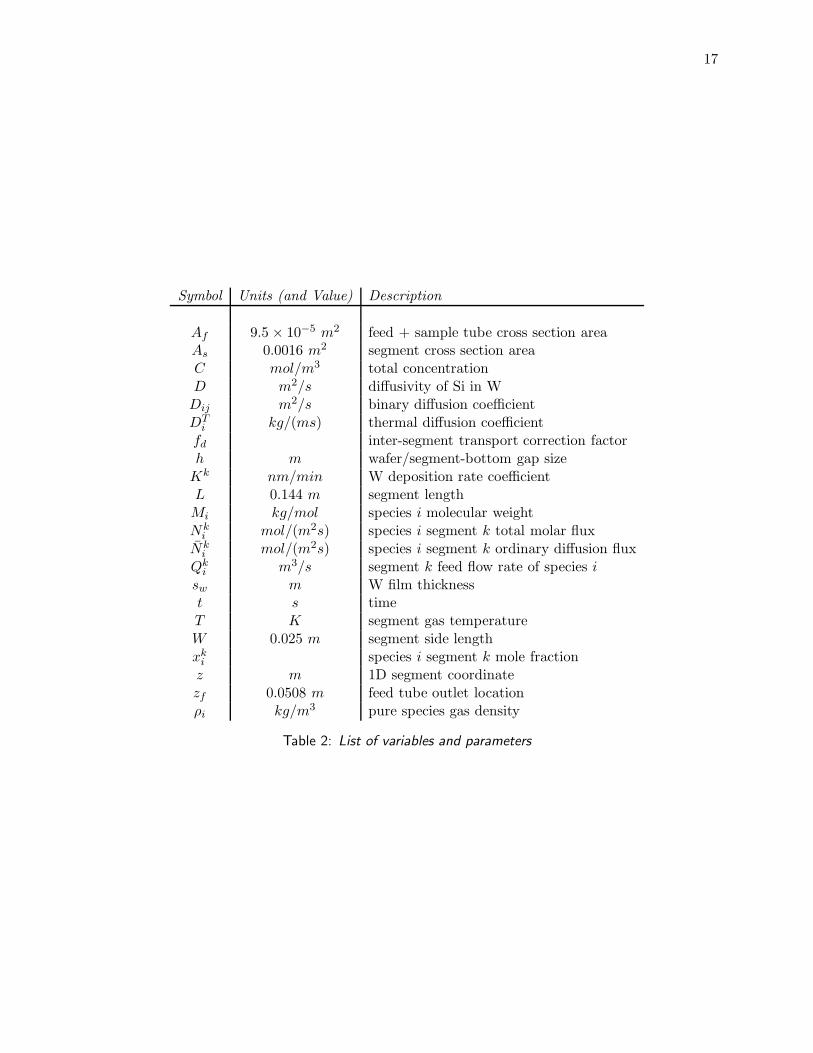
and Werner 1993; Reid et al. 1987). C is the total gas concentration. A complete summary of the
parameters and variables used is presented in Table 2 at the end of this paper.
These values of inter-segment species flux then are used as the initial value of the intra-segment
flux terms:
Nki (z) =
hW
As
3∑
n=1
Nk−ni + F k
i (z)
where F ki is a function accounting for the change in flux due to fresh feed of species i from the
segment feed tubes and is defined by
F ki = 0 z < zf
F ki = Qk
i ρi/(Mi(As − Af )) z ≥ zf
where Qki is the volumetric flowrate of gas species i to segment k.
10
3.3 Intra-segment transport
Neglecting any effect of pressure and forced diffusion, the multicomponent gas species transport can
be expressed by the Maxwell-Stefan equation
∇xki =
n∑
j=1
1
CDij
(
xki Nk
j − xkj Nk
i
)
+
n∑
j=1
xki xk
j
Dij
(
DTj
ρj−
DTi
ρi
)
∇ ln T 0 < z < L
subject to boundary conditions
xki (L) = xexh
i . (2)
The gas temperature profile along the segment length z is needed to compute the contribution
of thermal diffusion; observation of the W film deposited on the segment structure after a number of
experimental runs indicates that there is significant gas and segment heating along the bottom-most
third of the honeycomb segments. Given this observation, the gas temperature was approximated as
a linear interpolation between the wafer (maintained at 350oC) and the ambient temperature (30oC)
over the bottom third of the segment, and was set as the ambient temperature for the remainder of
the segment.
The flux due to ordinary diffusion can be defined as
N̄ki = Nk
i +DT
i
Mi∇ ln T
giving the simplified form of the Maxwell-Stefan equation
∇xki =
n∑
j=1
1
CDij
(
xki N̄k
j − xkj N̄k
i
)
(3)
subject to boundary conditions (2). The DTi are the multicomponent thermal diffusion coefficients
computed using the correlations given in Kleijn and Werner (1993).
4 Simulation Results
The nine inter-segment flux equations (1) are solved simultaneously with the nine collocation-
discretized Maxwell-Stefan equations (3) subject to boundary conditions (2) using a Newton-Raphson
method to obtain the gas composition profiles as a function of position within each segment. 20 col-
location points located at the zeros of 19th-degree Chebyshev polynomial, plus the interval endpoints,
were used to define the discretization arrays (Adomaitis 2002).
Because the modeling equations for each segment are identical in structure and vary only in
terms of parameter values, an object-oriented approach was taken to setting up the simulator: a

11
segment model class (in MATLAB) was derived from an abstract class defining the general structure
of a nonlinear algebraic equation model. Methods for the nonlinear equation model class included
a Newton-Raphson based equation solver, which is inherited by the segment model class. Because
each segment model is an instance of the latter class, this approach is an efficient method for setting
up models of this form, and is readily extensible to Programmable Reactor models with many more
segment elements. More details on the computational approach will be given in a later paper.
Representative results of this solution procedure are shown in Fig. 10. In this Figure, the wafer
surface is located at z = 0 (the left axis limit) and the segment top is to the right; the vertical
line represents the location zf of the bottom of the feed tube bundle inside each segment. Two
sets of simulations were performed to assess the effect total gas flow to each segment has on the
composition profiles, and the results are discussed below. In each case, the gap size h was set to
0. Simulations to evaluate the effect of gap size h will be performed later in this paper to interpret
some of the experimental findings.
4.1 Low-flow results
Simulator predictions for the gas composition profiles of Segments 1 to 3 (ordered from the top
plot) for a gas feed flow of Q = 2.5sccm to each segment are shown in the left column of plots in
Fig. 10. The composition in each segment as z → L approaches the composition of the gas in the
common, well-mixed exhaust chamber. As the profiles are followed down the segments, the feed gas
species of each segment becomes the primary component. However, because of the relatively low
flow, significant back-diffusion of the other components occurs resulting in a significant fraction of
each species being found near the bottom of each segment - this is particularly true in Segment 3
because of the larger fraction of H2 and the larger values of binary diffusion coefficients when H2 is
one of the species. It is also interesting to observe the effect thermal diffusion has in this simulation
- in each case, the region near the wafer is enriched in H2 relative to the heavier species due to
thermal diffusion. Thus, because of the large negative effect ordinary and thermal diffusion have on
the ability to control gas composition near the wafer surface, it is possible to conclude that higher
feed flow rates should be used.
4.2 High-flow results
Increasing the gas flowrate to 50sccm in each segment has a dramatic effect on the gas composition
profiles in each segment. As can be seen in the right column plots of Fig. 10, the feed species to

12
each segment becomes the dominant gas phase species near the wafer surface. Thermal diffusion
effects still can be observed, but have a much lower impact on the composition profiles. Under these
operating conditions, the effect of changing the gap size on gas composition near the wafer surface
should be more pronounced, and so initial experiments were conducted at these conditions. It should
be noted that the while the WF6 concentration at the bottom of Segments 1 and 3 is very small, it
is nontrivial and so can (and does) result in film deposition under these segments.
5 Prototype Experimental Tests
Initial experiments were performed using the three zone prototype to validate two basic Programmable
Reactor design concepts: (1) that the reverse-flow showerhead design could maintain significant
segment-to-segment gas-phase compositional differences near the wafer surface, and (2) that spatially
patterned wafers could be produced by this reactor design and that some of the characteristics of the
pattern can be controlled by manipulating the showerhead/wafer gap. Typical operating conditions
for the first experiments consisted of a 0.5 torr chamber pressure, a wafer temperature of 350oC, and
10-20 minute deposition times. The film thickness in the region below each segment was determined
by sheet resistance measurements using a four-point probe.
5.1 Segment-to-segment gas composition differences
In the set of experiments discussed in this paper, pure Ar was fed to Segment 1 at a flowrate of
50sccm; 50sccm of WF6 was fed to segment 2, and 50sccm of H2 was fed to segment 3. Sheet
resistance measurements were made at seven points on the wafer surface in each segment region; the
data are interpolated and plotted in Fig. 11. Simulator predictions for these conditions indicate that
the gas composition at the wafer surface is mainly the segment feed species, with a small amount of
WF6 present at the bottom of segments even when h = 0 (Fig. 10). While W deposition should take
place directly under Segment 2 (where pure WF6 is fed) due to the Si reduction mechanism, it is
interesting to note that some W deposition takes place under the remaining two segments. Further
experimental data and simulator predictions will validate that the WF6 responsible for deposition
in segments 1 and 3 is transported to this region through a combination in back-diffusion and
inter-segment diffusion.

13
5.2 Control of pattern resolution
In all cases where the showerhead/wafer spacing was small (e.g., h = 1mm), distinct hexagonal film
patterns were produced (Fig. 12). As the gap is increased, the contribution of back-diffusion down
the segments from the common exhaust remains essentially constant while inter-segment diffusion in
the gap region increases. Photographs of wafers processed for three different gap values are shown
in Fig. 12 demonstrating that the pattern becomes more diffused with increasing gap size. This
decrease in the sharpness of the deposition pattern provides visual evidence for the effectiveness of
using gap size to control inter-segment diffusion of reactant species across the wafer surface.
Across-wafer diffusion of WF6 from Segment 2 to the Ar- and H2-fed segments should result in
a negative film thickness gradient along lines drawn through the latter two segments in the direction
away from Segment 2 (as seen in the two lines marked in Fig. 11). This is clearly evident in the
linear interpolation plots presented in Fig. 13, where the film thickness along these two “cuts” in
Segments 1 and 3 is plotted for three different values of gap size. Furthermore, we observe the
overall thickening of the film in these two segments as the gap increases, a phenomenon attributable
to the increased WF6 concentration resulting from increasing inter-segment diffusion as the gap
is increased. Likewise, extrapolating the growth rates of Segments 1 and 3 to h = 0 (which is
an undesirable experiment to perform) shows positive growth rates in each segment for zero gap,
indicating the contribution of intra-segment back-diffusion of WF6 to the growth rate in each of
these segments. It is interesting to note the greater slope of the deposition rate line (as a function
of h) in Segment 1 relative to Segment 3; this may be attributable to the smaller binary diffusion
coefficient in an Ar-WF6 mixture compared to a H2-WF6 mixture.
Finally, error bars indicating the standard deviation of all seven sheet resistance measurements
per segment are plotted; the slightly increasing trend with gap size may indicate additional effects of
inter-segment and chamber-segment diffusion on film thickness variation within each segment region
as the gap increases. For increasing values of very large values of h (e.g., < 10mm), the variability
should begin to decrease with h due to the dominance of across-wafer diffusion under these operating
conditions.
6 Simulation-Based Interpretation of Film Deposition Results
Thin films of tungsten can be deposited in either a selective or blanket tungsten deposition mode.
The gas phase reactions associated with these deposition processes are negligible due to low reactor

14
pressure during the process operation (Arora and Pollard 1991; Kleijn et al. 1991), therefore, the
deposition rate is determined only by surface reaction and chemical species transport rates in the
gas/wafer surface interface and through the deposited film itself.
The overall reaction of tungsten deposition by hydrogen reduction on a silicon wafer substrate
begins with surface reactions by Si reduction during the film nucleation step; the reaction is
2 WF6(g) + 3Si(s) −→ 2W(s) + 3SiF4(g)
in the range of deposition temperature used in our experiments (Leusink et al. 1992). Numerous
studies have focused on the extent to which this reaction takes place and when the transition to the
H2 reduction process
WF6(g) + 3H2(s) −→ W(s) + 6HF(g)
occurs. Most studies conclude the Si reduction step is self limiting and typically accounts for 10-
200nm of W film thickness at the Si substrate/W film interface (Groenen et al. 1994). However,
Joshi et al. (1992) presented a counterexample study in which non-self-limited growth was observed
using two different CVD systems, resulting in relatively thick W films. A mechanism for this de-
position process was proposed whereby Si out-diffused from the substrate through the deposited W
film and reacted with WF6 on the film surface; this process was found to be promoted by oxygen
impurities in the W film. The expression for the overall deposition rate was determined to be the
product
dsw
dt= RkRd
(after eq. A5 in Joshi et al. 1992) where the rate of change of film thickness sw is the product of
the reaction rate of Si with WF6 at the film’s top surface
Rk =K0
NSi[CxWF6
]ne−Ea/RT (4)
and the rate at which Si atoms diffuse from the substrate through the W layer to the film surface:
Rd =C0
1 + K0sw[CxWF6]ne−Ea/RT /D
.
See Joshi et al. (1992) for a complete description of the parameters in these rate expressions. For
short deposition times or thin films (sw → 0) produced by low deposition temperature or low WF6
concentration, the term describing the rate of diffusion becomes a constant and the deposition rate is
determined only by the surface reaction rate Rk (in the absence of gas-phase transport limitations).
15
6.1 Simulated vs. measured deposition rates
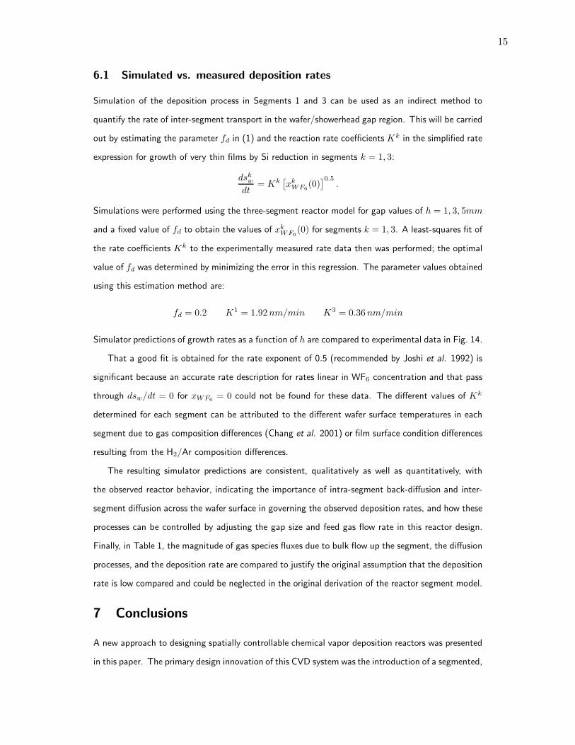
Simulation of the deposition process in Segments 1 and 3 can be used as an indirect method to
quantify the rate of inter-segment transport in the wafer/showerhead gap region. This will be carried
out by estimating the parameter fd in (1) and the reaction rate coefficients Kk in the simplified rate
expression for growth of very thin films by Si reduction in segments k = 1, 3:
dskw
dt= Kk
[
xkWF6
(0)]0.5
.
Simulations were performed using the three-segment reactor model for gap values of h = 1, 3, 5mm
and a fixed value of fd to obtain the values of xkWF6
(0) for segments k = 1, 3. A least-squares fit of
the rate coefficients Kk to the experimentally measured rate data then was performed; the optimal
value of fd was determined by minimizing the error in this regression. The parameter values obtained
using this estimation method are:
fd = 0.2 K1 = 1.92 nm/min K3 = 0.36 nm/min
Simulator predictions of growth rates as a function of h are compared to experimental data in Fig. 14.
That a good fit is obtained for the rate exponent of 0.5 (recommended by Joshi et al. 1992) is
significant because an accurate rate description for rates linear in WF6 concentration and that pass
through dsw/dt = 0 for xWF6= 0 could not be found for these data. The different values of Kk
determined for each segment can be attributed to the different wafer surface temperatures in each
segment due to gas composition differences (Chang et al. 2001) or film surface condition differences
resulting from the H2/Ar composition differences.
The resulting simulator predictions are consistent, qualitatively as well as quantitatively, with
the observed reactor behavior, indicating the importance of intra-segment back-diffusion and inter-
segment diffusion across the wafer surface in governing the observed deposition rates, and how these
processes can be controlled by adjusting the gap size and feed gas flow rate in this reactor design.
Finally, in Table 1, the magnitude of gas species fluxes due to bulk flow up the segment, the diffusion
processes, and the deposition rate are compared to justify the original assumption that the deposition
rate is low compared and could be neglected in the original derivation of the reactor segment model.
7 Conclusions
A new approach to designing spatially controllable chemical vapor deposition reactors was presented
in this paper. The primary design innovation of this CVD system was the introduction of a segmented,

16
Flux Value, mol/(m2s)
convective (F ki ) O(10−2)
intra- and inter-segment (N j−ki ) O(10−5)
deposition rate O(10−7)
Table 1: A comparison of fluxes predicted by the reactor simulator.
reverse-flow gas delivery (showerhead) assembly. A three segment prototype reactor was constructed
to prove the validity of the design concept and provide engineering data for simulator development.
Preliminary experimental testing demonstrated the validity of the design by depositing spatially
patterned films using the reactor’s ability to control across wafer gas composition. Simulation
studies were performed to interpret experimental data and to estimate gas phase composition at the
wafer surface.
This approach to thin-film manufacturing control opens the door to a new generation of CVD
reactor design, allowing single-wafer combinatorial studies and precise across-wafer uniformity con-
trol in a single reactor design. The modular nature of the showerhead segments offers the possibility
of developing CVD reactors for very large substrates. To reach these goals, a new reactor is under
construction that includes a more precisely controllable reactant gas delivery system, a cleaner re-
action chamber environment, and better access to the wafer while the deposition process is taking
place. It is anticipated that the additional instrumentation in the next prototype will allow a demon-
stration of the programmability capabilities envisioned for this system. Research in improving the
manufacturability of the showerhead segment modules, particularly integrating feed gas flow control
into each segment, also is in progress.
8 Acknowledgments
The authors acknowledge the support of the National Science Foundation through grant CTS-
0085632 for construction of the prototype and simulation work, the continued support of NSF
through CTS-0219200, and National Institute of Standards and Technology for fabricating several
showerhead components.
17
Symbol Units (and Value) Description
Af 9.5 × 10⁻⁵ m2 feed + sample tube cross section areaAs 0.0016 m2 segment cross section areaC mol/m3 total concentrationD m2/s diffusivity of Si in WDij m2/s binary diffusion coefficientDT
i kg/(ms) thermal diffusion coefficientfd inter-segment transport correction factorh m wafer/segment-bottom gap size
Kk nm/min W deposition rate coefficientL 0.144 m segment lengthMi kg/mol species i molecular weightNk
i mol/(m2s) species i segment k total molar fluxN̄k
i mol/(m2s) species i segment k ordinary diffusion fluxQk
i m3/s segment k feed flow rate of species isw m W film thicknesst s timeT K segment gas temperatureW 0.025 m segment side lengthxk
i species i segment k mole fractionz m 1D segment coordinatezf 0.0508 m feed tube outlet locationρi kg/m3 pure species gas density
Table 2: List of variables and parameters
18
9 References
Adomaitis, R. A. (2002) Objects for MWR, Comp. & Chem. Engng 26 7-8, 981-998.
Arora, R. and R. Pollard, (1991) A mathematical model for chemical vapor deposition process influ-
enced by surface reaction kinetics: application to low-pressure deposition of tungsten, J. Electrochem.
Soc. 38 (5) 1523.
Banks, H. T., S. C. Beeler, G. M. Kepler, and H. T. Tran (2002) Reduced order modeling and control
of thin film growth in an HPCVD reactor, SIAM J. Appl. Math. 62 1251-1280.
Chang, H. -Y., R. A. Adomaitis, J. N. Kidder, Jr., and G. W. Rubloff (2001) Influence of gas
composition on wafer temperature in a tungsten chemical vapor deposition reactor: Experimental
measurements, model development, and parameter estimation, J. Vac. Sci. and Tech.,B 19 230-238.
Christofides, P. D. (2001) Nonlinear and Robust Control of PDE Systems: Methods and Applications
to Transport-Reaction Processes, Birkhauser Pub. Co.
Gadgil, P. N., Optimization of a stagnation point flow reactor design for metalorganic chemical vapor
deposition by flow visualization (1993) J. Crystal Growth 134 302-312.
Gougousi, T., Y. Xu, J.N. Kidder, Jr., G. W. Rubloff, and C. R. Tilford (2000) Process diagnostics
and thickness metrology for the chemical vapor deposition of W from H2/WF6 using in-situ mass-
spectrometry, J. Vac. Sci. Technol. B 18, 1352-1363
Groenen, P. A. C., J. G. A. Holscher, and H. H. Brongersma, (1994) Mechanism of the reaction of
WF6 and Si, Applied Surface Sci 78, 123-132.
Ireland, P. J., (1997) High aspect ratio contacts: A review of the current tungsten plug process,
Thin Solid Films 304, 1-12.
Joshi, R. V., V. Prasad, M. L. Yu, and G. Scilla, (1992) Non-self-limiting nature of silicon reduction
of WF6 in cold wall systems, J. Appl. Phys. 71 (3) 1428-1441.
Kepler, G. M., H. T. Tran, and H. T. Banks (2000) Reduced order model compensator control of
species transport in a CVD reactor, Optim. Contr. Appl. Meth. 21 143-160.
Kepler, G. M., H. T. Tran, and H. T. Banks (2001) Compensator control for chemical vapor depo-
sition film growth using reduced-order design models, IEEE Tran. Semicond. Manuf. 14 231-241.
Kiether, W. J., M. J. Fordham, S. Yu, A. J. S. Neto, K. A. Conrad, J. Hauser, F. Y. Sorrell, and
J. J. Wortman (1994) Three-Zone Rapid Thermal Processor System. Proc. 2nd Int. RTP Conf.,
96-101.
Kim B. N. and H. H. Lee, Numerical simulation of metalorganic chemical vapor deposition of copper
in a single-wafer reactor (1997) J. Electrochem.Soc. 144 1765-1773.
Kleijn, C. R., (2000) Computational modeling of transport phenomena and detailed chemistry in
chemical vapor deposition - a benchmark solution, Thin Solid Films 365, 294-306.
Kleijn, C. R., C. J. Hoogendoorn, A. Hasper, J. Holleman and J. Middelhoek, (1991) Transport
phenomena in tungsten LPCVD in a single-wafer reactor, J. Electrochem. Soc. 138, 509-517.
Kleijn, C. R., Th. H. van der Meer, and C. J. Hoogendoorn, (1989) A mathematical model for
LPCVD in a single wafer reactor, J. Electrochem. Soc. 136, 3423-3433.
Kleijn C. R. and C. Werner, (1993) Modeling of chemical vapor deposition of tungsten films, Basel;
Boston: Birkhauser Verlag.
Kobayashi, A., A. Sekiguchi, K. Ikeda, O. Okada, N. Hosokawa, Y. Tsuchiya, and K. Ueno, The
deposition rate for Cu CVD. (1997) In Advanced Metalization and Interconnect Systems for ULSI
Applications, ed. by R. Havemann, J. Schmitz, H. Komiyama, and K. Tsubouchi, Mater. Res. Soc.
Pittsburgh, PA, 177-183.

19
Leusink, G. J., C. R. Kleijn, T. G. M. Oosterlaken, C. A. M. Janssen, and S. Radelaar, (1992)
Growth kinetics and inhibition of growth of chemical vapor deposited thin tungsten films on silicon
from tungsten hexafluoride, J. Appl. Phys. 72 (2) 490-498.
Moffat, H. K. and K. F. Jensen, (1988) Three-dimensional flow effects in silicon CVD in horizontal
reactor, J. Electrochem. Soc. 135, 459-471.
Moslehi, M. M., C. J. Davis, and A. Bowling, TI Technical Journal, Sept-Oct 1992, 44-64.
Moslehi, M. M, C. J. Davis, and R. T. Matthews, (1995) Programmable multizone gas injector for
single-wafer semiconductor processing equipment, United State Patent 5,453,124.
Reid, R. C., J. M. Praunitz and B. E. Poling, (1987) The properties of gases and liquids (4th edition),
New York, McGraw-Hill.
Stuber, J. D., I. Trachtenburg, and T. F. Edgar, Design and modeling of rapid thermal processing
systems (1998) IEEE Trans. Semicond. Manuf. 11 442-457.
Theodoropoulos, C., T. J. Mountziaris, H. K. Moffat and J. Han, (2000) Design of gas inlets for the
growth of gallium nitride by metalorganic vapor phase epitaxy, J. Crystal Growth 217, 65-81.
Theodoropoulou, A., E. Zafiriou, and R. A. Adomaitis (1999) Inverse model based real-time control
for temperature uniformity of RTCVD, IEEE Trans. Semicond. Manuf. 12, 87-101.
van der Stricht, W., I. Moerman, P. Demeester, J. A. Crawley and E. J. Thrush, (1997) Study of
GaN and InGaN films grown by metalorganic chemical vapor deposition, J. Crystal Growth 170,
344-348.
Wang, C. A., S. H. Gorves, S. C. Palmateer, D. W. Weyburne, and R. A. Brown, (1986) Flow
visualization studies of OMVPE reactor designs J. Crystal Growth 77 136-147.
Xia, L., P. W. Lee, M. Chang, I. Latchford, P. K. Narwankar, R. Urdahl, (2000) Chapter 11.
Chemical Vapor Deposition, Handbook of Semiconductor Manufacturing Technology, Yoshi Nishi,
Robert Doering, ed., New York: Marcel Dekker.
Yang, C., C. Huang, G. Chi and M. Wu, (1998) Growth and characterization of GaN by atmosphere
pressure metalorganic chemical-vapor deposition with a novel separate-flow reactor, J. Crystal Growth
200 39-44.

20
Figure 1: An illustration of the Programmable CVD Reactor three-zone prototype showing the seg-mented showerhead structure and segment feed lines.
Figure 2: A rapid process prototyping approach to new materials and process development. The spatialpatterning capabilities of the Programmable CVD Reactor can be used to produce a “library” wafer(left) containing regions of distinct material properties; the reactor system then can be reprogrammedto deposit spatially uniform films of the chosen property (right).
Figure 3: Gas concentration field computed for a segmented showerhead design illustrating the mis-match between gas injector location and the resulting gas concentration profile over the wafer surfacein a non-reverse flow design.
Figure 4: Periodic flow patterns generated by the reverse flow showerhead design.
Figure 5: Simulation of gas concentration profile over the wafer surface by a two-zone reverse flowdesign; note smooth concentration gradient over the wafer surface.
Figure 6: The two-chamber Ulvac W CVD cluster tool modified to accommodate the prototypeshowerhead assembly.
Figure 7: Schematic diagram showing a vertical cross-section of the Programmable CVD reactor.
Figure 8: The prototype showerhead mounted on one of the Ulvac reactor chambers.
Figure 9: Details of a single showerhead segment.
Figure 10: Gas composition profiles in each segment for two different gas flow rates for the Ar fedsegment (top), WF6 fed segment (middle), and H2 fed segment (bottom); the vertical line marks thefeed tube bundle outlet location.
Figure 11: Film thickness measurements for a representative experiment determined by sheet resistancemeasurements. Seven measurements were made in each segment region.
Figure 12: Deposition patterns produced using three different values for the showerhead/wafer spacing.In these experiments pure Ar, WF6, and H2 were fed to the individual segments.
Figure 13: Film thickness measurements for three showerhead/wafer spacing values showing how filmthickness shrinks in the Ar and H2 fed segments with distance from the WF6 segment (left) and howoverall film thickness increases in each segment region as the spacing is increased (right)
Figure 14: Simulated predictions of the W deposition rate by Si reduction in the Ar and H2 fed segmentscompared to experimental measurements.

Figure 1

Figure 2
Library wafer:programmed nonuniformity
Uniform depositionat specified conditions
Figure 3
Annular-segmented showerhead gas inlets
Gas
out
let
Inert Reactant InertCha
mbe
r ce
nter
line
Heated stage
Wafer

Figure 4
Gas inlet
Gasoutlets
Gasoutlets
Figure 5

Figure 6

Figure 7

Figure 8

Figure 9
wafer surfaceat z = -h
z = 0
z = zf
z = L
W
Af
Qik
Nik
As
Figure 10

Figure 11

Figure 12
1mm 3mm 5mm
Increasing across-wafer diffusion
32
1
32
1
32
1

Figure 13
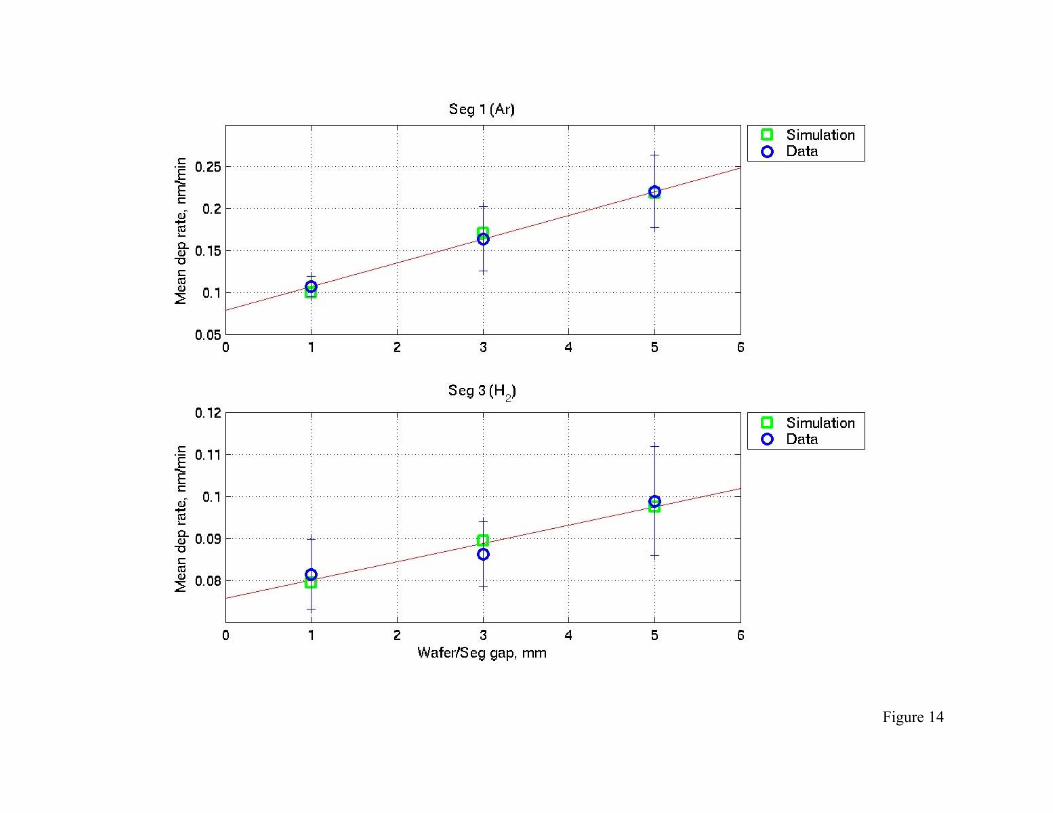
Figure 14