spc56elxx/rpc56elxx adc built-in self-tests adc … · spc56elxx/rpc56elxx adc built-in self-tests...
TRANSCRIPT
October 2015 DocID025337 Rev 2 1/29
AN4371Application note
SPC56ELxx/RPC56ELxx ADC Built-in self-tests ADC working inCPU mode
IntroductionIn automotive more and more often comes in foreground the question of safety. For this reason the ST’s PowerPC microcontrollers are embedded with various self-test features and procedures. This document provides detailed view on ADC built-in self-tests (BIST’s), along with demonstration examples to guide the customer for correct use of the ADC BIST’s.
www.st.com
Contents AN4371
2/29 DocID025337 Rev 2
Contents
1 ADC built-in self-test . . . . . . . . . . . . . . . . . . . . . . . . . . . . . . . . . . . . . . . . . 51.1 ADC Built-in self-test description . . . . . . . . . . . . . . . . . . . . . . . . . . . . . . . . 5
1.2 ADC self-test important note . . . . . . . . . . . . . . . . . . . . . . . . . . . . . . . . . . . 6
1.3 ADC calibration data . . . . . . . . . . . . . . . . . . . . . . . . . . . . . . . . . . . . . . . . . . 6
1.4 Reading from Test Flash . . . . . . . . . . . . . . . . . . . . . . . . . . . . . . . . . . . . . . 61.4.1 Flash content . . . . . . . . . . . . . . . . . . . . . . . . . . . . . . . . . . . . . . . . . . . . . . 8
2 ADC built-in self-test algorithms . . . . . . . . . . . . . . . . . . . . . . . . . . . . . . 102.1 Self-test execution flow . . . . . . . . . . . . . . . . . . . . . . . . . . . . . . . . . . . . . . 10
2.2 Supply self-test – Algorithm S . . . . . . . . . . . . . . . . . . . . . . . . . . . . . . . . . 112.2.1 Supply self-test in CPU mode . . . . . . . . . . . . . . . . . . . . . . . . . . . . . . . . 14
2.3 Resistive-Capacitive self-test - Algorithm RC . . . . . . . . . . . . . . . . . . . . . . 162.3.1 Resistive-Capacitive self-test in CPU mode . . . . . . . . . . . . . . . . . . . . . 16
2.4 Capacitive self-test - Algorithm C . . . . . . . . . . . . . . . . . . . . . . . . . . . . . . . 182.4.1 Capacitive self-test in CPU mode . . . . . . . . . . . . . . . . . . . . . . . . . . . . . 18
3 Appendix A . . . . . . . . . . . . . . . . . . . . . . . . . . . . . . . . . . . . . . . . . . . . . . . . 203.1 Test Flash copy function example . . . . . . . . . . . . . . . . . . . . . . . . . . . . . . 20
3.2 Algorithm S example in CPU scan mode . . . . . . . . . . . . . . . . . . . . . . . . . 20
3.3 Algorithm RC example in CPU one-shot mode . . . . . . . . . . . . . . . . . . . . 22
3.4 Algorithm RC example in CPU scan mode . . . . . . . . . . . . . . . . . . . . . . . . 23
3.5 Algorithm C example in CPU one-shot mode . . . . . . . . . . . . . . . . . . . . . . 24
3.6 Algorithm C example in CPU scan mode . . . . . . . . . . . . . . . . . . . . . . . . . 25
Appendix A Reference document . . . . . . . . . . . . . . . . . . . . . . . . . . . . . . . . . . . . . 27
Revision history . . . . . . . . . . . . . . . . . . . . . . . . . . . . . . . . . . . . . . . . . . . . . . . . . . . . 28

DocID025337 Rev 2 3/29
AN4371 List of tables
3
List of tables
Table 1. Test Flash Content . . . . . . . . . . . . . . . . . . . . . . . . . . . . . . . . . . . . . . . . . . . . . . . . . . . . . . . . 8Table 2. Typical values stored in Test sector of Flash memory . . . . . . . . . . . . . . . . . . . . . . . . . . . . . 8Table 3. Sampling phase duration for the test conversions . . . . . . . . . . . . . . . . . . . . . . . . . . . . . . . 10Table 4. Sample phase settings . . . . . . . . . . . . . . . . . . . . . . . . . . . . . . . . . . . . . . . . . . . . . . . . . . . . 10Table 5. Document revision history. . . . . . . . . . . . . . . . . . . . . . . . . . . . . . . . . . . . . . . . . . . . . . . . . . 28
List of figures AN4371
4/29 DocID025337 Rev 2
List of figures
Figure 1. ADC block diagram. . . . . . . . . . . . . . . . . . . . . . . . . . . . . . . . . . . . . . . . . . . . . . . . . . . . . . . . 6Figure 2. Test Flash reading . . . . . . . . . . . . . . . . . . . . . . . . . . . . . . . . . . . . . . . . . . . . . . . . . . . . . . . . 7Figure 3. Self-test execution sequence example C and RC in scan mode . . . . . . . . . . . . . . . . . . . . 11Figure 4. Self-test execution sequence flow example S in scan mode . . . . . . . . . . . . . . . . . . . . . . . 11Figure 5. Self-test baud rate example C and RC . . . . . . . . . . . . . . . . . . . . . . . . . . . . . . . . . . . . . . . . 11Figure 6. ADC self-test Algorithm S . . . . . . . . . . . . . . . . . . . . . . . . . . . . . . . . . . . . . . . . . . . . . . . . . . 13Figure 7. ADC self-test configuration – Algorithm S. . . . . . . . . . . . . . . . . . . . . . . . . . . . . . . . . . . . . . 14Figure 8. Example test execution flow for Algorithm S. . . . . . . . . . . . . . . . . . . . . . . . . . . . . . . . . . . . 15Figure 9. Test execution flow - Algorithm S . . . . . . . . . . . . . . . . . . . . . . . . . . . . . . . . . . . . . . . . . . . . 16Figure 10. Self-test flow in one-shot mode- algorithm RC . . . . . . . . . . . . . . . . . . . . . . . . . . . . . . . . . . 17Figure 11. Test flow - Algorithm RC. . . . . . . . . . . . . . . . . . . . . . . . . . . . . . . . . . . . . . . . . . . . . . . . . . . 17Figure 12. Self-test flow in one-shot mode- algorithm C . . . . . . . . . . . . . . . . . . . . . . . . . . . . . . . . . . . 19
DocID025337 Rev 2 5/29
AN4371 ADC built-in self-test
28
1 ADC built-in self-test
For safety relevant applications, it is important to perform the ADC functionality check at regular intervals(a). For this purpose, hardware build in self testing feature has been incorporated inside the ADC. Tests at application level can be used in place of the ADC self-test to verify the integrity of the ADC itself. It is a user's tasks to choose the counter-measure which better fits his needs.
Three types of Self Testing algorithms have been implemented inside ADC analog. Supply Self test: Algorithm S Resistive-Capacitive Self test: Algorithm RC Capacitive Self test: Algorithm C
The built-in self-tests use analog watchdogs to verify the result of self-test conversions. During the production factory testing, accurate threshold values for these watchdogs are stored in the Test sector of the flash memory. Each testing algorithm contains its own threshold values. Each microcontroller has its own threshold values. Most values are identical or very similar across the microcontrollers. The build-in self-tests can be executed in CPU mode as well as in CTU (Cross Triggering Unit) mode(b).
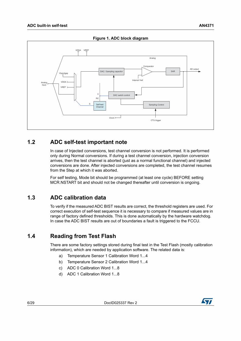
1.1 ADC Built-in self-test descriptionThe ADC implements a channel (self-test channel) dedicated for self-testing. The self-test schedule is done via special set of self-test registers in ADC. ADC also offers capability of monitoring the converted data using analog watchdog registers and flags the error to the Fault Collection and Control Unit (FCCU) in case any of the algorithms fails.
a. depending on the specific safety concept, the ADC self-test can be run only once after the boot
b. this AN focuses on ADC working in CPU mode
ADC built-in self-test AN4371
6/29 DocID025337 Rev 2
Figure 1. ADC block diagram
1.2 ADC self-test important noteIn case of Injected conversions, test channel conversion is not performed. It is performed only during Normal conversions. If during a test channel conversion, injection conversion arrives, then the test channel is aborted (just as a normal functional channel) and injected conversions are done. After injected conversions are completed, the test channel resumes from the Step at which it was aborted.
For self testing, Mode bit should be programmed (at least one cycle) BEFORE setting MCR.NSTART bit and should not be changed thereafter until conversion is ongoing.
1.3 ADC calibration dataTo verify if the measured ADC BIST results are correct, the threshold registers are used. For correct execution of self-test sequence it is necessary to compare if measured values are in range of factory defined thresholds. This is done automatically by the hardware watchdog. In case the ADC BIST results are out of boundaries a fault is triggered to the FCCU.
1.4 Reading from Test FlashThere are some factory settings stored during final test in the Test Flash (mostly calibration information), which are needed by application software. The related data is:
a) Temperature Sensor 1 Calibration Word 1...4b) Temperature Sensor 2 Calibration Word 1...4c) ADC 0 Calibration Word 1...8d) ADC 1 Calibration Word 1...8
DocID025337 Rev 2 7/29
AN4371 ADC built-in self-test
28
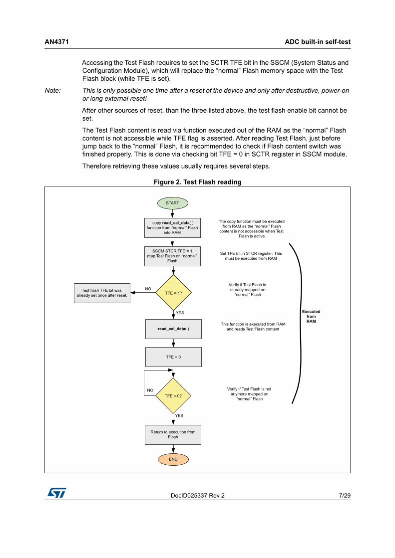
Accessing the Test Flash requires to set the SCTR TFE bit in the SSCM (System Status and Configuration Module), which will replace the “normal” Flash memory space with the Test Flash block (while TFE is set).
Note: This is only possible one time after a reset of the device and only after destructive, power-on or long external reset!
After other sources of reset, than the three listed above, the test flash enable bit cannot be set.
The Test Flash content is read via function executed out of the RAM as the “normal” Flash content is not accessible while TFE flag is asserted. After reading Test Flash, just before jump back to the “normal” Flash, it is recommended to check if Flash content switch was finished properly. This is done via checking bit TFE = 0 in SCTR register in SSCM module.
Therefore retrieving these values usually requires several steps.
Figure 2. Test Flash reading
ADC built-in self-test AN4371
8/29 DocID025337 Rev 2
1.4.1 Flash contentFlash memory Test sector contains calibration and other chip-specific data. This information is summarized in Table 1 below.
Table 1. Test Flash ContentAddress Word name Function
0x0000 TSENS_0_CAL W2/W4 TSENS_0 Calibration data W2 (P2/PTAT) and W4 (C2/CTAT) at cold temperature
0x0004 TSENS_1_CAL W2/W4 TSENS_1 Calibration data W2 (P2/PTAT) and W4 (C2/CTAT) at cold temperature
0x0008 TSENS_0_CAL W1/W3 TSENS_0 Calibration data W1 (P1/PTAT) and W3 (C1/CTAT) at hot temperature
0x000C TSENS_1_CAL W1/W3 TSENS_1 Calibration data W1 (P1/PTAT) and W3 (C1/CTAT) at hot temperature
0x0010 ADC0_CAL W1 ADC0 Self-Test calibration - RC algo
0x0014 ADC0_CAL W2 ADC0 Self-Test calibration - C algo S0 step
0x0018 ADC0_CAL W3 ADC0 Self-Test calibration - C algo Sn step
0x001C ADC0_CAL W4 ADC0 Self-Test calibration - S algo S0 step - 3.3 V
0x0020 ADC0_CAL W5 ADC0 Self-Test calibration - S algo S0 step - 5.0 V
0x0024 ADC0_CAL W6 ADC0 Self-Test calibration - S algo S1 step - integer
0x0028 ADC0_CAL W7 ADC0 Self-Test calibration - S algo S1 step - float
0x002C ADC0_CAL W8 ADC0 Self-Test calibration - S algo S2 step
0x0030 ADC0 Reserved ADC0 reserved
0x0034 ADC1_CAL W1 ADC1 Self-Test calibration - RC algo
0x0038 ADC1_CAL W2 ADC1 Self-Test calibration - C algo S0 step
0x003C ADC1_CAL W3 ADC1 Self-Test calibration - C algo Sn step
0x0040 ADC1_CAL W4 ADC1 Self-Test calibration - S algo S0 step - 3.3 V
0x0044 ADC1_CAL W5 ADC1 Self-Test calibration - S algo S0 step - 5.0 V
0x0048 ADC1_CAL W6 ADC1 Self-Test calibration - S algo S1 step - integer
0x004C ADC1_CAL W7 ADC1 Self-Test calibration - S algo S1 step - float
0x0050 ADC1_CAL W8 ADC1 Self-Test calibration - S algo S2 step
0x0054 ADC1 Reserved ADC1 Reserved
Table 2. Typical values stored in Test sector of Flash memory
WordFlash
location offset
Value in flash Loads to STAWxR Step THRH THRL
W1 10h 0xFE20F1E0 STAW3R RC 0xE20h 0x1E0h
W2 14h 0xF856F732 STAW4R C0 0x856h 0x732h
DocID025337 Rev 2 9/29
AN4371 ADC built-in self-test
28
Note: These values are unique for each sample.
W3 18h 0xF873F732 STAW5R C1-C17 0x873h 0x732h
W4 1Ch 0xF75AF4DF STAW0R S0_3.3V 0x75Ah 0x4DFh
W5 20h 0xF4D0F2DB STAW0R S0_5.0V 0x4D0h 0x2DBh
W6 24h 0xF003F002 STAW1AR S1(INT) 0x3h 0x2h
W7 28h 0xF3D9F1E3 STAW1BR S1(FRAC) 0x3D9h 0x1E3h
W8 2Ch 0xFFFFFFF9 STAW2R S2 0xFFFh 0xFF9h
Table 2. Typical values stored in Test sector of Flash memory (continued)
WordFlash
location offset
Value in flash Loads to STAWxR Step THRH THRL
ADC built-in self-test algorithms AN4371
10/29 DocID025337 Rev 2
2 ADC built-in self-test algorithms
ADC contains three self test algorithms in order to test its functionality.
The SPC56xx/RPC56xx uses two types of parameter settings to define the ADC self-test operation: Sample phase duration settings programmed into the INPSAMP_S, INPSAMP_RC,
and INPSAMP_C fields of the Self-Test Configuration Register (STCR1). Threshold values for analog watchdog algorithms
In order to support different loading and switching times, several different conversion timing registers (CTR) are present. There is one register per channel type.
Table 2 represents the typical values for INPSAMP_x register. For detailed description of INPSAMP_x calculation please refer to the Reference Manual.
Recommended setting for INPSAMP_S is the maximum value of this register field due to slow sample capacitor setting time at low temperature for S0 algorithm.
2.1 Self-test execution flowThe number of channels converted at the end of each chain is 1 (except for Algorithm S, in which all the steps are performed at once without any functional conversion interleaved). In Scan Mode, consecutive steps of selected self test algorithm are converted continuously at the end of each chain of normal conversions.
Table 3. Sampling phase duration for the test conversions
INPSAMP_C
Sampling phase duration for the test conversions related to the algorithm C. Valid self-test values for this field are given below.Minimum: 0x18Maximum: 0xFF
INPSAMP_RC
Sampling phase duration for the test conversions related to the algorithm RC. Valid self-test values for this field are given below.Minimum: 0x60Maximum: 0xFF
INPSAMP_S
Sampling phase duration for the test conversions related to the algorithm S. Valid self-test values for this field are given below.Minimum: 0xFFMaximum: 0xFF
Table 4. Sample phase settingsRegister field Recommended setting
INPSAMP_C 0x18h
INPSAMP_RC 0x60h
INPSAMP_S 0xFFh
DocID025337 Rev 2 11/29
AN4371 ADC built-in self-test algorithms
28
Figure 3. Self-test execution sequence example C and RC in scan mode
Figure 4. Self-test execution sequence flow example S in scan mode
In the case it is required to schedule self-test channel execution in a defined sequence the baud rate is implemented in ADC. This control defines the scheduling of test channel between the normal conversions. The scheduling rate is specified by STBRR[BR].
Figure 5. Self-test baud rate example C and RC
By default, if test channel is enabled, one Step of selected algorithm is executed after every chain of normal conversion. STBRR[BR] field provides flexibility by scheduling the test channel conversion to be performed not at the end of every chain but at the end of BR+1 number of chains.
Note: This feature is applicable only for scan mode of operation and not for one shot mode. The STBRR.BR should be set to zero for one shot mode.
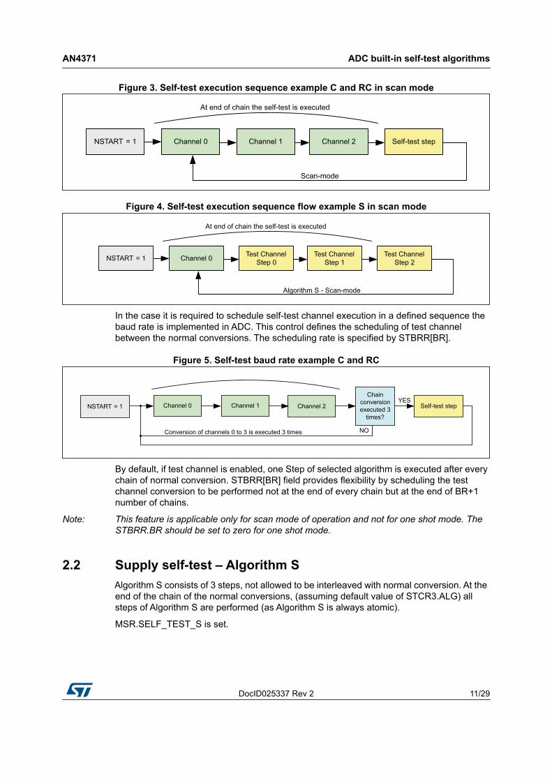
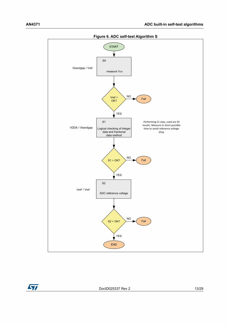
2.2 Supply self-test – Algorithm SAlgorithm S consists of 3 steps, not allowed to be interleaved with normal conversion. At the end of the chain of the normal conversions, (assuming default value of STCR3.ALG) all steps of Algorithm S are performed (as Algorithm S is always atomic).
MSR.SELF_TEST_S is set.
ADC built-in self-test algorithms AN4371
12/29 DocID025337 Rev 2
It includes the conversion of: ADC internal bandgap voltage (S0 - step0) – (Vbandgap / Vref) ADC supply voltage (S1 - step1) – (VDDA / Vbandgap) ADC reference voltage (S2 - step2) – (Vref'(c) / Vref)
c. Vref’ is an internal positive reference voltage.
DocID025337 Rev 2 13/29
AN4371 ADC built-in self-test algorithms
28
Figure 6. ADC self-test Algorithm S
ADC built-in self-test algorithms AN4371
14/29 DocID025337 Rev 2
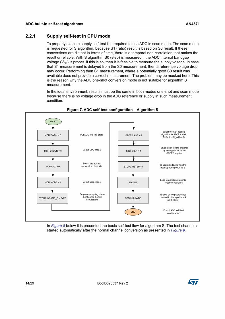
2.2.1 Supply self-test in CPU modeTo properly execute supply self-test it is required to use ADC in scan mode. The scan mode is requested for S algorithm, because S1 (ratio) result is based on S0 result. If these conversions are distant in terms of time, there is a temporal non-correlation that makes the result unreliable. With S algorithm S0 (step) is measured if the ADC internal bandgap voltage (Vref) is proper. If this is so, then it is feasible to measure the supply voltage. In case that S1 measurement is delayed from the S0 measurement, then a reference voltage drop may occur. Performing then S1 measurement, where a potentially good S0 result was available does not provide a correct measurement. The problem may be masked here. This is the reason why the ADC one-shot conversion mode is not suitable for algorithm S measurement.
In the ideal environment, results must be the same in both modes one-shot and scan mode because there is no voltage drop in the ADC reference or supply in such measurement condition.
Figure 7. ADC self-test configuration – Algorithm S
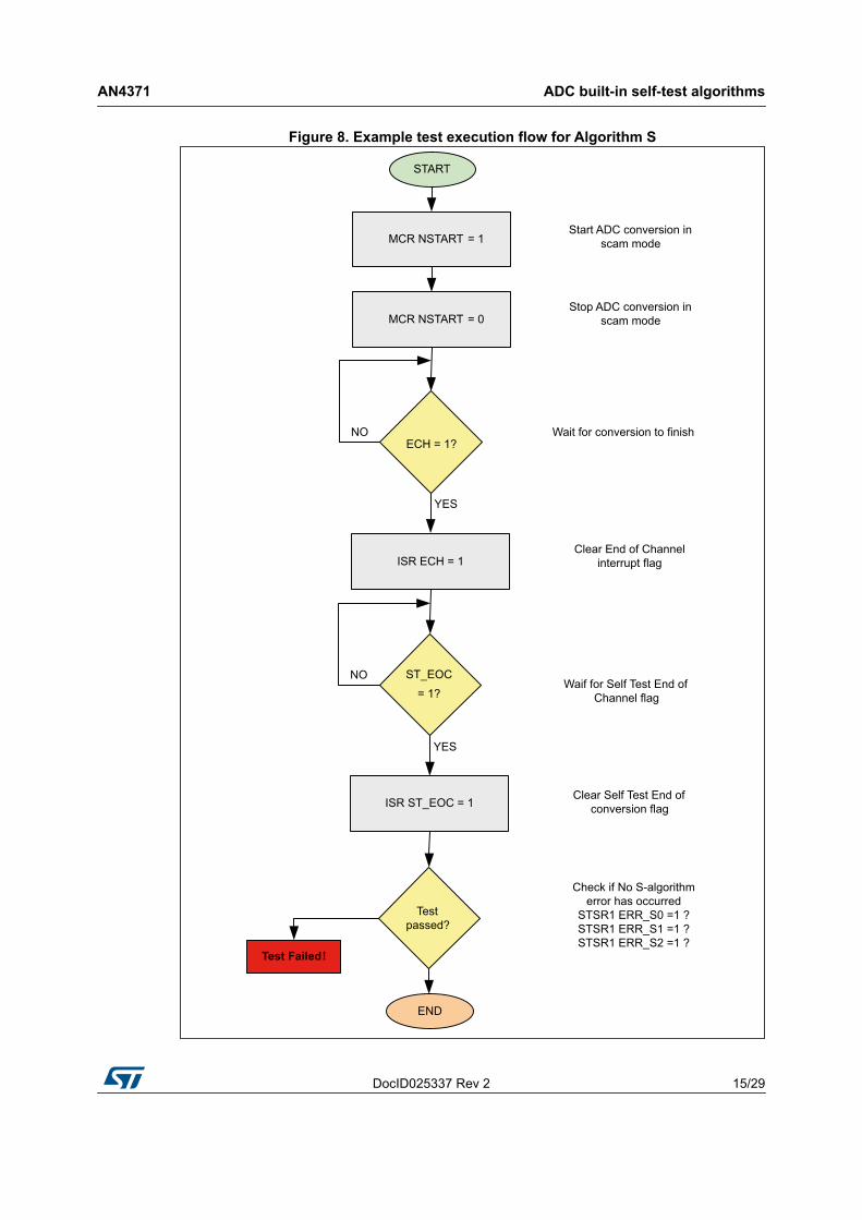
In Figure 8 below it is presented the basic self-test flow for algorithm S. The test channel is started automatically after the normal channel conversion as presented in Figure 9.
DocID025337 Rev 2 15/29
AN4371 ADC built-in self-test algorithms
28
Figure 8. Example test execution flow for Algorithm S
ADC built-in self-test algorithms AN4371
16/29 DocID025337 Rev 2
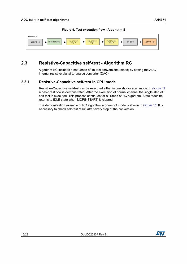
Figure 9. Test execution flow - Algorithm S
2.3 Resistive-Capacitive self-test - Algorithm RCAlgorithm RC includes a sequence of 19 test conversions (steps) by setting the ADC internal resistive digital-to-analog converter (DAC).
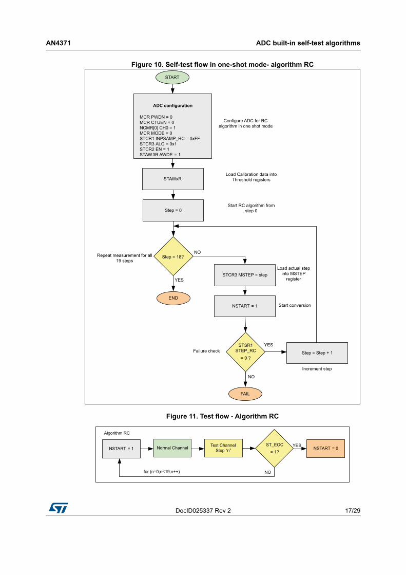
2.3.1 Resistive-Capacitive self-test in CPU modeResistive-Capacitive self-test can be executed either in one shot or scan mode. In Figure 11 a basic test flow is demonstrated. After the execution of normal channel the single step of self-test is executed. This process continues for all Steps of RC algorithm. State Machine returns to IDLE state when MCR[NSTART] is cleared.
The demonstration example of RC algorithm in one-shot mode is shown in Figure 10. It is necessary to check self-test result after every step of the conversion.
DocID025337 Rev 2 17/29
AN4371 ADC built-in self-test algorithms
28
Figure 10. Self-test flow in one-shot mode- algorithm RC
Figure 11. Test flow - Algorithm RC
ADC built-in self-test algorithms AN4371
18/29 DocID025337 Rev 2
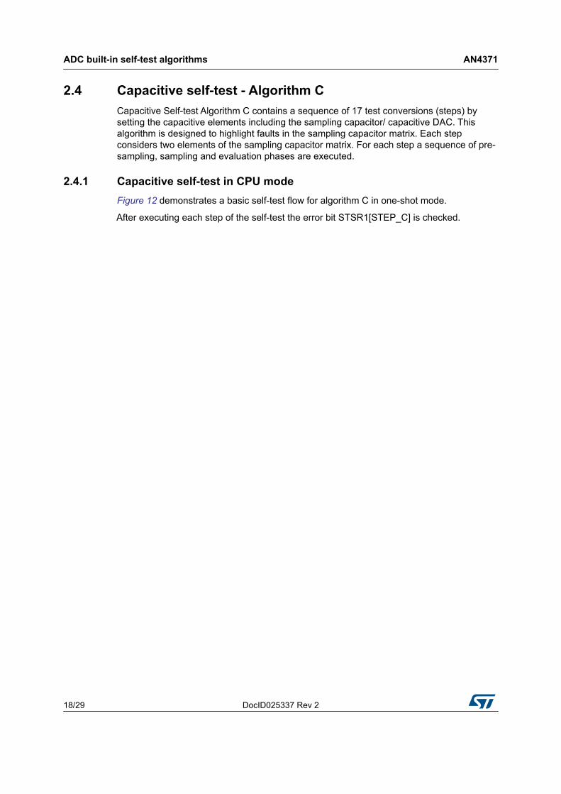
2.4 Capacitive self-test - Algorithm CCapacitive Self-test Algorithm C contains a sequence of 17 test conversions (steps) by setting the capacitive elements including the sampling capacitor/ capacitive DAC. This algorithm is designed to highlight faults in the sampling capacitor matrix. Each step considers two elements of the sampling capacitor matrix. For each step a sequence of pre-sampling, sampling and evaluation phases are executed.
2.4.1 Capacitive self-test in CPU modeFigure 12 demonstrates a basic self-test flow for algorithm C in one-shot mode.
After executing each step of the self-test the error bit STSR1[STEP_C] is checked.
DocID025337 Rev 2 19/29
AN4371 ADC built-in self-test algorithms
28
Figure 12. Self-test flow in one-shot mode- algorithm C
Appendix A AN4371
20/29 DocID025337 Rev 2
3 Appendix A
Example source code can be found in these appendixes.
3.1 Test Flash copy function exampleRead_Self_Test_calibration_data function is necessary to be executed from RAM.
#pragma ghs section text=".ramcode"
void Read_Self_Test_calibration_data (void)
{
uint32_t address = 0x0;
uint32_t i = 0;
/* map Test Flash sector into Flash memory stating 0x0 */
SSCM.SCTR.B.TFE = 1;
for (i=0;i<22;i++)
{
Raw_Test_Flash_Calibration_Data[i] = (*(volatile uint32_t *)address);
address = address + 0x4;
}
SSCM.SCTR.B.TFE = 0;
}
#pragma ghs section
3.2 Algorithm S example in CPU scan modevoid ADC0_SUPPLY_SELF_TEST_ScanMode(void){ // Algorithm S ADC0.MCR.B.PWDN = 0; // Enable ADC0 /* 1 */ ADC0.MCR.B.CTUEN = 0; // CPU mode
/* 2 */
ADC0.NCMR[0].B.CH0 = 1; // ADC0 channel 0 is set. Program NCMR0 to select channels to be converted for normal conversion
/* 3 */
DocID025337 Rev 2 21/29
AN4371 Appendix A
28
ADC0.MCR.B.MODE = 1; // Program MCR[MODE] = 1 to select Scan Mode mode
/* 4 */
ADC0.STCR1.B.INPSAMP_S = 0xFF; // Program sampling phase duration for the test conversions
/* 5 */
ADC0.STCR3.B.ALG = 0x0; // Select the Self Testing algorithm in STCR3.ALG. Default is Algorithm S
/* 6 */
ADC0.STCR2.B.EN = 1; // ADC0 Enable self testing channel by setting EN bit in the STCR2 register
/* 7 */
/* Step 0 - ADC0 internal bandgap voltage register configuration */
ADC0.STCR3.B.MSTEP = 0; // For Scan-shot mode, defines the first step for algorithms S
ADC0.STAW0R.B.THRL = ADC0_Self_Test_Flash_Calibration_Data[6]; // Set ADC0 Self-Test calibration data - S algo S0 step - 3.3V
ADC0.STAW0R.B.THRH = ADC0_Self_Test_Flash_Calibration_Data[7]; // Set ADC0 Self-Test calibration data - S algo S0 step - 3.3V
ADC0.STAW0R.B.AWDE = 1; // Enable analog watchdog related to the algorithm S (step 0)
/* Step 1 - ADC supply voltage register configuration */
/* Integer */
ADC0.STAW1AR.B.THRL = ADC0_Self_Test_Flash_Calibration_Data[10]; // Set ADC0 Self-Test calibration data - S algo S1 step - (integer) - Low Treshold Value
ADC0.STAW1AR.B.THRH = ADC1_Self_Test_Flash_Calibration_Data[11]; // Set ADC0 Self-Test calibration data - S algo S1 step - (integer) - High Treshold Value
/* Float */
ADC0.STAW1BR.B.THRL = ADC0_Self_Test_Flash_Calibration_Data[12]; // Set ADC0 Self-Test calibration data - S algo S1 step - (float) - Low Treshold Value
ADC0.STAW1BR.B.THRH = ADC0_Self_Test_Flash_Calibration_Data[13];
ADC0.STAW1AR.B.AWDE = 1; // Enable analog watchdog related to the algorithm S (step 1)
/* Step 2 - ADC reference voltage register configuration */
ADC0.STAW2R.B.THRL = ADC0_Self_Test_Flash_Calibration_Data[14]; // Set ADC0 Self-Test calibration data - S algo S2 step) - Low Treshold Value
ADC0.STAW2R.B.AWDE = 1; // Enable analog watchdog related to the algorithm S (step 2)
ADC0.MCR.B.NSTART = 1; // Start ADC0 normal conversion by setting NSTART bit in the MCR
ADC0.MCR.B.NSTART = 0; // Stop ADC0 normal conversion by setting NSTART bit in the MCR
while (ADC0.ISR.B.ECH == 0);
ADC0.ISR.B.ECH = 1;
while (ADC0.STSR1.B.ST_EOC == 0);
Appendix A AN4371
22/29 DocID025337 Rev 2
ADC0.STSR1.B.ST_EOC = 1;
if (ADC0.STSR1.B.ERR_S0 == 1 || ADC0.STSR1.B.ERR_S1 == 1 || ADC0.STSR1.B.ERR_S2 == 1) // Check if No S-algorithm error has occurred
{
while(1); // Self test failed
}
/* 8 */
// On receiving end of conversion for test channel, the digital result is written in
// STDR1.TCDATA and STDR1.VALID bit is set. Also, EOC and ECH bits are set in the
// ISR and ST_EOC bit is set in STSR1.
/* 9 */
// State Machine returns to IDLE state.
}
3.3 Algorithm RC example in CPU one-shot modevoid ADC0_RESISTIVE_CAPACITIVE_SELF_TEST (void)
{
uint8_t step = 0;
// Algorithm RC
ADC0.MCR.B.PWDN = 0; // Enable ADC0
/* 1 */
ADC0.MCR.B.CTUEN = 0; // CPU mode
/* 2 */
ADC0.NCMR[0].B.CH0 = 1; // ADC0 channel 0 is set. Program NCMR0 to select channels to be converted for normal conversion
/* 3 */
ADC0.MCR.B.MODE = 0; // Program MCR[MODE] = 0 to select one shot mode
/* 4 */
ADC0.STCR1.B.INPSAMP_RC = 0xFF; // Program sampling phase duration for the test conversions
/* 5 */
ADC0.STCR3.B.ALG = 0x1; // Select the RC Self Testing algorithm in STCR3.ALG. Default is Algorithm S
/* 6 */
ADC0.STCR2.B.EN = 1; // ADC0 Enable self testing channel by setting EN bit in the STCR2 register
/* 7 */
ADC0.STAW3R.B.AWDE = 1; // Enable analog watchdog related to the algorithm RC
/* 8 */
DocID025337 Rev 2 23/29
AN4371 Appendix A
28
ADC0.STAW3R.B.THRL = ADC0_Self_Test_Flash_Calibration_Data[0]; // ADC0 Self-Test calibration - RC algo - Low Treshold Value
ADC0.STAW3R.B.THRH = ADC0_Self_Test_Flash_Calibration_Data[1]; // ADC0 Self-Test calibration - RC algo - High Treshold Value
/* 9 */
for(step=0;step<19;step++)
{
ADC0.STCR3.B.MSTEP = step; // For one-shot mode, defines the current step for algorithms S
ADC0.MCR.B.NSTART = 1; // Start ADC0 normal conversion by setting NSTART bit in the MCR
if (ADC1.STSR1.B.STEP_RC != 0)
{
ADC_Self_Test_Fail[step+6] = 1; // Check if No RC-algorithm [step] error has occurred
}
}
}
3.4 Algorithm RC example in CPU scan modevoid ADC0_RESISTIVE_CAPACITIVE_SELF_TEST_ScanMode (void)
{
// Algorithm RC
ADC0.MCR.B.PWDN = 0; // Enable ADC0
/* 1 */
ADC0.MCR.B.CTUEN = 0; // CPU mode
/* 2 */
ADC0.NCMR[0].B.CH0 = 1; // ADC0 channel 0 is set. Program NCMR0 to select channels to be converted for normal conversion
/* 3 */
ADC0.MCR.B.MODE = 1; // Program MCR[MODE] = 0 to select one scan mode
/* 4 */
ADC0.STCR1.B.INPSAMP_RC = 0xFF; // Program sampling phase duration for the test conversions
/* 5 */
ADC0.STCR3.B.ALG = 0x1; // Select the RC Self Testing algorithm in STCR3.ALG. Default is Algorithm S
/* 6 */
ADC0.STCR2.B.EN = 1; // ADC0 Enable self testing channel by setting EN bit in the STCR2 register
/* 7 */
ADC0.STAW3R.B.AWDE = 1; // Enable analog watchdog related to the algorithm RC
/* 8 */
Appendix A AN4371
24/29 DocID025337 Rev 2
ADC0.STAW3R.B.THRL = ADC0_Self_Test_Flash_Calibration_Data[0]; // ADC0 Self-Test calibration - RC algo - Low Treshold Value
ADC0.STAW3R.B.THRH = ADC0_Self_Test_Flash_Calibration_Data[1]; // ADC0 Self-Test calibration - RC algo - High Treshold Value
/* 9 */
ADC0.MCR.B.NSTART = 1; // Start ADC0 normal conversion by setting NSTART bit in the MCR
while (ADC0.STSR1.B.ST_EOC != 0);
ADC0.MCR.B.NSTART = 0; // Stop ADC0 normal conversion by setting NSTART bit in the MCR
if (ADC0.STSR1.B.STEP_RC != 0) // Check if No RC-algorithm error has occurred
{
while(1); // Self test failed
}
ADC0.STSR1.B.ST_EOC = 0;
}
3.5 Algorithm C example in CPU one-shot modevoid ADC1_CAPACITIVE_SELF_TEST (void)
{
uint8_t step = 0;
// Algorithm C
ADC1.MCR.B.PWDN = 0; // Enable ADC1
/* 1 */
ADC1.MCR.B.CTUEN = 0; // CPU mode
/* 2 */
ADC1.NCMR[0].B.CH0 = 1; // ADC_0 channel 0 is set. Program NCMR0 to select channels to be converted for normal conversion
/* 3 */
ADC1.MCR.B.MODE = 0; // Program MCR[MODE] = 0 to select one shot mode
/* 4 */
ADC1.STCR1.B.INPSAMP_C = 0xFF; // Program sampling phase duration for the test conversions
/* 5 */
ADC1.STCR3.B.ALG = 0x2; // Select the Self Testing algorithm in STCR3.ALG. Default is Algorithm S
/* 6 */
ADC1.STCR2.B.EN = 1; // ADC_0 Enable self testing channel by setting EN bit in the STCR2 register
/* 7 */
DocID025337 Rev 2 25/29
AN4371 Appendix A
28
ADC1.MCR.B.NSTART = 1; // Start ADC1 normal conversion by setting NSTART bit in the MCR
/* 8 */
ADC1.STAW4R.B.THRL = ADC1_Self_Test_Flash_Calibration_Data[2]; // ADC1 Self-Test calibration - C algo S0 step) - Low Treshold Value
ADC1.STAW4R.B.THRH = ADC1_Self_Test_Flash_Calibration_Data[3]; // ADC1 Self-Test calibration - C algo S0 step) - High Treshold Value
ADC1.STAW5R.B.THRL = ADC1_Self_Test_Flash_Calibration_Data[4]; // ADC1 Self-Test calibration - C algo Sn step) - Low Treshold Value
ADC1.STAW5R.B.THRH = ADC1_Self_Test_Flash_Calibration_Data[5]; // ADC1 Self-Test calibration - C algo Sn step) - High Treshold Value
for(step=0;step<17;step++)
{
ADC1.STCR3.B.MSTEP = step; // For one-shot mode, defines the current step for algorithms S
ADC1.MCR.B.NSTART = 1; // Start ADC1 normal conversion by setting NSTART bit in the MCR
if (ADC1.STSR1.B.STEP_C != 0)
{
ADC_Self_Test_Fail[step+60] = 1; // Check if No RC-algorithm [step] error has occurred
}
}
}
3.6 Algorithm C example in CPU scan modevoid ADC0_CAPACITIVE_SELF_TEST_ScanMod (void)
{
// Algorithm C
ADC0.MCR.B.PWDN = 0; // Enable ADC0
/* 1 */
ADC0.MCR.B.CTUEN = 0; // CPU mode
/* 2 */
ADC0.NCMR[0].B.CH0 = 1; // ADC_0 channel 0 is set. Program NCMR0 to select channels to be converted for normal conversion
/* 3 */
ADC0.MCR.B.MODE = 1; // Program MCR[MODE] = 0 to select one shot mode
/* 4 */
ADC0.STCR1.B.INPSAMP_C = 0xFF; // Program sampling phase duration for the test conversions
/* 5 */
ADC0.STCR3.B.ALG = 0x2; // Select the Self Testing algorithm in STCR3.ALG. Default is Algorithm S
/* 6 */
ADC0.STCR2.B.EN = 1; // ADC_0 Enable self testing channel by setting EN bit in the STCR2 register
Appendix A AN4371
26/29 DocID025337 Rev 2
/* 7 */
ADC0.STAW4R.B.THRL = ADC0_Self_Test_Flash_Calibration_Data[2]; // ADC0 Self-Test calibration - C algo S0 step) - Low Treshold Value
ADC0.STAW4R.B.THRH = ADC0_Self_Test_Flash_Calibration_Data[3]; // ADC0 Self-Test calibration - C algo S0 step) - High Treshold Value
ADC0.STAW5R.B.THRL = ADC0_Self_Test_Flash_Calibration_Data[4]; // ADC0 Self-Test calibration - C algo Sn step) - Low Treshold Value
ADC0.STAW5R.B.THRH = ADC0_Self_Test_Flash_Calibration_Data[5]; // ADC0 Self-Test calibration - C algo Sn step) - High Treshold Value
/* 8 */
ADC0.MCR.B.NSTART = 1; // Start ADC0 normal conversion by setting NSTART bit in the MCR
while (ADC0.STSR1.B.ST_EOC != 0);
ADC0.MCR.B.NSTART = 0; // Stop ADC0 normal conversion by setting NSTART bit in the MCR
if (ADC0.STSR1.B.STEP_C != 0) // Check if No C-algorithm error has occurred
{
while(1); // Self test failed
}
ADC0.STSR1.B.ST_EOC = 0;
}
DocID025337 Rev 2 27/29
AN4371 Reference document
28
Appendix A Reference document
SPC56ELxx Reference manual (Doc ID 15265)

Revision history AN4371
28/29 DocID025337 Rev 2
Revision history
Table 5. Document revision historyDate Revision Changes
02-Oct-2013 1 Initial release.
08-Oct-2015 2 Robust root part numbers added.
DocID025337 Rev 2 29/29
AN4371
29
IMPORTANT NOTICE – PLEASE READ CAREFULLY
STMicroelectronics NV and its subsidiaries (“ST”) reserve the right to make changes, corrections, enhancements, modifications, and improvements to ST products and/or to this document at any time without notice. Purchasers should obtain the latest relevant information on ST products before placing orders. ST products are sold pursuant to ST’s terms and conditions of sale in place at the time of order acknowledgement.
Purchasers are solely responsible for the choice, selection, and use of ST products and ST assumes no liability for application assistance or the design of Purchasers’ products.
No license, express or implied, to any intellectual property right is granted by ST herein.
Resale of ST products with provisions different from the information set forth herein shall void any warranty granted by ST for such product.
ST and the ST logo are trademarks of ST. All other product or service names are the property of their respective owners.
Information in this document supersedes and replaces information previously supplied in any prior versions of this document.
© 2015 STMicroelectronics – All rights reserved