sri venkateswara college of enginnering & technology
TRANSCRIPT

1
SRI VENKATESWARA COLLEGE OF ENGINNERING & TECHNOLOGY
(AUTONOMOUS)
(AFFILIATED TO JNTUA, ANANTAPUR)
ACADEMIC REGULATIONS
M.TECH REGULAR 2 YEAR DEGREE PROGRAMME
(FOR THE BATCHES ADMITTED FROM THE ACADEMIC YEAR 2015-16)
The Jawaharlal Nehru Technological University Anantapur shall confer M.Tech Post
Graduate degree to candidates who are admitted to the Master of Technology Programs and fulfill
all the requirements for the award of the degree.
1.0 ELIGIBILITY FOR ADMISSIONS:
Admission to the above programme shall be made subject to the eligibility, qualifications
and specialization prescribed by the competent authority for each programme, from time
to time. Admissions shall be made either on the basis of merit rank obtained by the qualified
candidates at an Entrance Test conducted by the University or on the basis of GATE/PGECET score,
subject to reservations and policies prescribed by the Government from time to time.
2.0 ADMISSION PROCEDURE:
As per the existing stipulations of AP State Council for Higher Education (APSCHE),
Government of Andhra Pradesh, admissions are made into the first year as follows:
a) Category –A seats are to be filled by Convener through PGECET/GATE score.
b) Category-B seats are to be filled by Management as per the norms stipulated by
Government of A.P.
3.0 Specializations:
Sl. No Department Specializations
1. CE Structural Engg.
2. EEE Power Electronics & Electrical Drives
3. EEE Electrical Power Systems
4. ME CAD/CAM
5. ME Machine Design
6. ECE VLSI System Design
7. ECE Digital Electronics and Communication System
8. ECE Embedded systems
9. CSE Computer Science & Engg.
10. CSE Computer Science
11. IT Software Engg.
2
4.0 COURSE WORK:
4.1. A Candidate after securing admission must pursue the M.Tech course of study for Four
Semesters duration.
4.2. Each semester shall have a minimum of 16 instructional weeks.
4.3. A candidate admitted to a programme should complete it within a period equal to twice the
prescribed duration of the programme from the date of admission.
5.0 ATTENDANCE:
5.1. A candidate shall be deemed to have eligibility to write end semester examinations if he has
put in at least 75% of attendance on cumulative basis of all subjects/courses in the
semester.
5.2. Condonation of shortage of attendance up to 10% i.e., from 65% and above and less than
75% may be given by the college on the recommendation of the Principal.
5.3. Condonation of shortage of attendance shall be granted only on medical grounds and on
representation by the candidate with supporting evidence.
5.4. If the candidate does not satisfy the attendance requirement he is detained for want of
attendance and shall reregister for that semester. He shall not be promoted to the next
semester.
6.0 EVALUATION:
The performance of the candidate in each semester shall be evaluated subject wise, with a
maximum of 100 marks for Theory and 100 marks for practical’s, on the basis of Internal
Evaluation and End Semester Examination.
6.1. For the theory subjects 60% of the marks will be for the External End Examination. While
40% of the marks will be for Internal Evaluation, based on the average of the marks
secured in the two Mid Term-Examinations held, one in the middle of the Semester (first
two units) and another immediately after the completion of instruction (last three units)
with four questions to be answered out of five in 2 hours, evaluated for 40 marks. For
semester end examination (external paper setting & external evaluation) five questions
shall be given for a maximum of 60 marks with one question from each unit with internal
choice i.e. either or type. All questions carry equal marks.
6.2. For practical subjects, 60 marks shall be for the End Semester Examinations and 40 marks
will be for internal evaluation based on the day to day performance (25 marks) and
practical test at the end of the semester (15 marks).
3
6.3. Seminar is a continuous assessment process. For Seminar there will be an internal
evaluation of 50 marks. A candidate has to secure a minimum of 50% to be declared
successful. The assessment will be made by a board consisting of HOD and two internal
experts.
6.4. For comprehensive viva voce there will be an internal evaluation of 100 marks. A
candidate has to secure a minimum of 50% to be declared successful. The assessment will
be made by a board consisting of HOD and two internal experts.
6.5. A candidate shall be deemed to have secured the minimum academic requirement in a
subject if he secures a minimum of 40% of marks in the End Examination and a minimum
aggregate of 50% of the total marks in the End Semester Examination and Internal
Evaluation taken together.
6.6. In case the candidate does not secure the minimum academic requirement in any of the
subjects (as specified in 6.5) he has to reappear for the Semester Examination either
supplementary or regular in that subject, or repeat the subject when next offered or do
any other specified subject as may be required.
6.7. Revaluation / Recounting:
Students shall be permitted for request for recounting/revaluation of the Semester-End
examination answer scripts within a stipulated period after payment of prescribed fee. After
recounting or revaluation, records are updated with changes if any and the student will be
issued a revised grade sheet. If there are no changes, the same will be intimated to the
students.
6.8 Supplementary Examination:
In addition to the regular Semester- End examinations conducted, the College may also schedule
and conduct supplementary examinations for all the subjects of other semesters when feasible
for the benefit of students. Such of the candidates writing supplementary examinations may have
to write more than one examination per day.
7.0 RE-REGISTRATION:
Following are the conditions to avail the benefit of improvement of internal
evaluation marks
7.1. The candidate should have completed the course work and obtained examinations results
for I & II semesters.
7.2. He should have passed all the subjects for which the Internal evaluation marks secured
are more than or equal to 50%.
4
7.3. Out of the subjects the candidate has failed in the examination due to Internal evaluation
marks secured being less than 50%, the candidate shall be given one chance for each
Theory subject and for a maximum of three Theory subjects for Improvement of Internal
evaluation marks.
7.4. The candidate has to re-register for the chosen subjects and fulfill the academic
requirements.
7.5. For each subject, the candidate has to pay a fee equivalent to one third of the semester
tuition fee and the along with the requisition to the Principal of the college.
7.6. In the event of availing the Improvement of Internal evaluation marks, the internal
evaluation marks as well as the End Examinations marks secured in the previous
attempt(s) for the reregistered subjects stand cancelled.
8.0 EVALUATION OF PROJECT WORK:
Every candidate shall be required to submit thesis or dissertation after taking up a topic
approved by the college/ institute.
8.1. Registration of Project work: A candidate is permitted to register for the project work after
satisfying the attendance requirement of I & II Semesters.
8.2. An Internal Departmental Committee (I.D.C) consisting of HOD, Supervisor and one
internal senior teacher shall monitor the progress of the project work.
8.3. The work on the project shall be initiated in the penultimate semester and continued in the
final semester. The duration of the project is for two semesters. The candidate can submit
Project thesis with the approval of I.D.C. after 36 weeks from the date of registration at the
earliest. Extension of time within the total permissible limit for completing the programme
is to be obtained from the Head of the Institution.
8.4. The student must submit status report at least in three different phases during the project
work period. These reports must be approved by the I.D.C before submission of the Project
Report and award internal assessment marks for 120.
8.5. A candidate shall be allowed to submit the Thesis / Dissertation only after passing in all the
prescribed subjects (both theory and practical) and then take viva voce examination of the
project. The viva voce examination may be conducted once in two months for all the
candidates who have submitted thesis during that period.
5
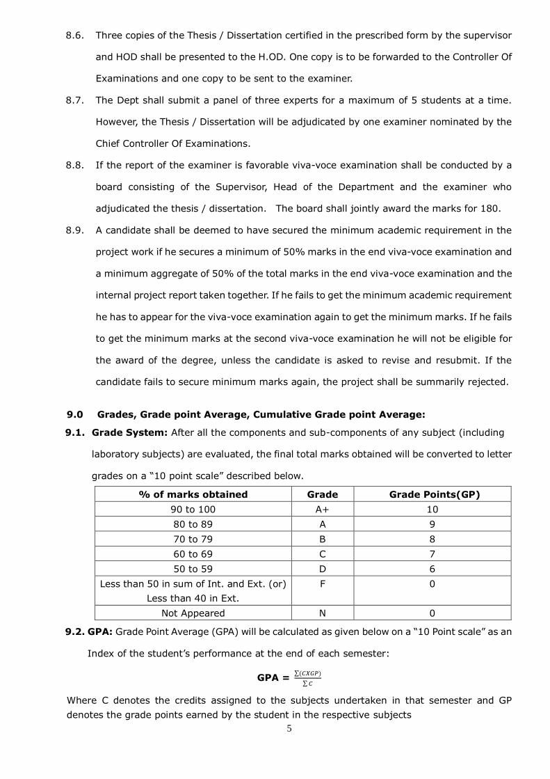
8.6. Three copies of the Thesis / Dissertation certified in the prescribed form by the supervisor
and HOD shall be presented to the H.OD. One copy is to be forwarded to the Controller Of
Examinations and one copy to be sent to the examiner.
8.7. The Dept shall submit a panel of three experts for a maximum of 5 students at a time.
However, the Thesis / Dissertation will be adjudicated by one examiner nominated by the
Chief Controller Of Examinations.
8.8. If the report of the examiner is favorable viva-voce examination shall be conducted by a
board consisting of the Supervisor, Head of the Department and the examiner who
adjudicated the thesis / dissertation. The board shall jointly award the marks for 180.
8.9. A candidate shall be deemed to have secured the minimum academic requirement in the
project work if he secures a minimum of 50% marks in the end viva-voce examination and
a minimum aggregate of 50% of the total marks in the end viva-voce examination and the
internal project report taken together. If he fails to get the minimum academic requirement
he has to appear for the viva-voce examination again to get the minimum marks. If he fails
to get the minimum marks at the second viva-voce examination he will not be eligible for
the award of the degree, unless the candidate is asked to revise and resubmit. If the
candidate fails to secure minimum marks again, the project shall be summarily rejected.
9.0 Grades, Grade point Average, Cumulative Grade point Average:
9.1. Grade System: After all the components and sub-components of any subject (including
laboratory subjects) are evaluated, the final total marks obtained will be converted to letter
grades on a “10 point scale” described below.
% of marks obtained Grade Grade Points(GP)
90 to 100 A+ 10
80 to 89 A 9
70 to 79 B 8
60 to 69 C 7
50 to 59 D 6
Less than 50 in sum of Int. and Ext. (or)
Less than 40 in Ext.
F 0
Not Appeared N 0
9.2. GPA: Grade Point Average (GPA) will be calculated as given below on a “10 Point scale” as an
Index of the student’s performance at the end of each semester:
GPA = ∑(𝐶𝑋𝐺𝑃)
∑ 𝐶
Where C denotes the credits assigned to the subjects undertaken in that semester and GP
denotes the grade points earned by the student in the respective subjects
6
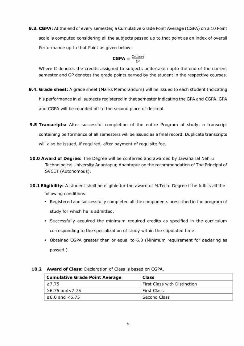
9.3. CGPA: At the end of every semester, a Cumulative Grade Point Average (CGPA) on a 10 Point
scale is computed considering all the subjects passed up to that point as an index of overall
Performance up to that Point as given below:
CGPA = ∑(𝐶𝑋𝐺𝑃)
∑ 𝐶
Where C denotes the credits assigned to subjects undertaken upto the end of the current
semester and GP denotes the grade points earned by the student in the respective courses.
9.4. Grade sheet: A grade sheet (Marks Memorandum) will be issued to each student Indicating
his performance in all subjects registered in that semester indicating the GPA and CGPA. GPA
and CGPA will be rounded off to the second place of decimal.
9.5 Transcripts: After successful completion of the entire Program of study, a transcript
containing performance of all semesters will be issued as a final record. Duplicate transcripts
will also be issued, if required, after payment of requisite fee.
10.0 Award of Degree: The Degree will be conferred and awarded by Jawaharlal Nehru
Technological University Anantapur, Anantapur on the recommendation of The Principal of
SVCET (Autonomous).
10.1 Eligibility: A student shall be eligible for the award of M.Tech. Degree if he fulfills all the
following conditions:
Registered and successfully completed all the components prescribed in the program of
study for which he is admitted.
Successfully acquired the minimum required credits as specified in the curriculum
corresponding to the specialization of study within the stipulated time.
Obtained CGPA greater than or equal to 6.0 (Minimum requirement for declaring as
passed.)
10.2 Award of Class: Declaration of Class is based on CGPA.
Cumulative Grade Point Average Class
≥7.75 First Class with Distinction
≥6.75 and<7.75 First Class
≥6.0 and <6.75 Second Class
7
11.0 WITHHOLDING OF RESULTS: If the candidate has not paid dues to the university or
If any case of in-discipline is pending against him, the result of the candidate shall be withheld
and he will not be allowed / promoted into the next higher semester. The issue of degree is liable
to be withheld in such cases.
12.0 TRANSITORY REGULATIONS:
Candidates who have discontinued or have been detained for want of attendance or who have
failed after having undergone the course in earlier regulations and wish to continue the course are
eligible for admission into the unfinished semester from the date of commencement of class work
with the same or equivalent subjects as and when subjects are offered, subject to 6.5 and 4.3
sections. Whereas they continue to be in the academic regulations of the batch they join later.
13.0 GENERAL:
i. The academic regulations should be read as a whole for purpose of any interpretation.
ii. Disciplinary action for Malpractice/improper conduct in examinations is appended.
iii. Where the words “he”, “him”, “his”, occur in the regulations, they include “she”, “her”,
“hers”.
iv. In the case of any doubt or ambiguity in the interpretation of the above rules, the
decision of the Principal is final.
v. The college may change or amend the academic regulations or syllabi at any time and the
changes or amendments shall be made applicable to all the students on rolls with effect
from the dates notified by the college.
*****
8
Sri Venkateswara College of Engineering And Technology (Autonomous)
R.V.S. Nagar, Chittoor
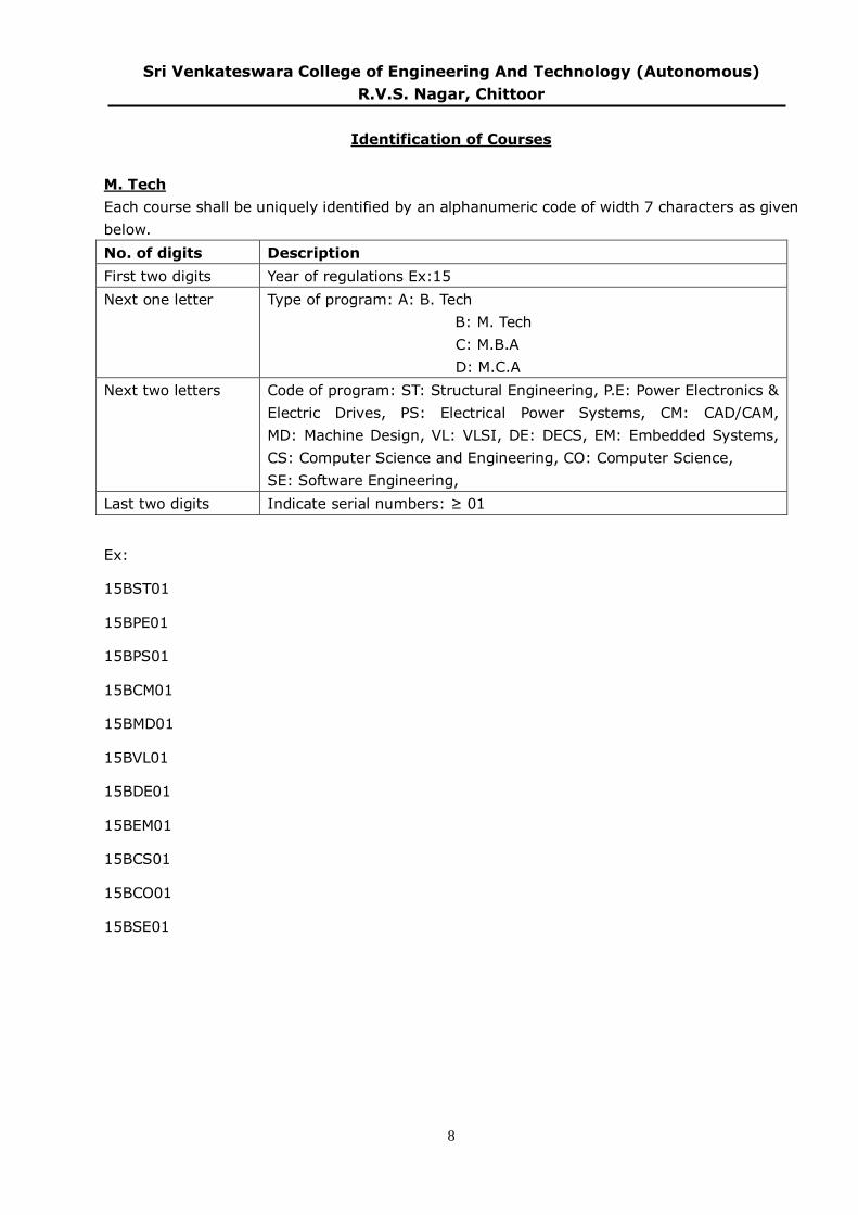
Identification of Courses
M. Tech
Each course shall be uniquely identified by an alphanumeric code of width 7 characters as given
below.
No. of digits Description
First two digits Year of regulations Ex:15
Next one letter Type of program: A: B. Tech
B: M. Tech
C: M.B.A
D: M.C.A
Next two letters Code of program: ST: Structural Engineering, P.E: Power Electronics &
Electric Drives, PS: Electrical Power Systems, CM: CAD/CAM,
MD: Machine Design, VL: VLSI, DE: DECS, EM: Embedded Systems,
CS: Computer Science and Engineering, CO: Computer Science,
SE: Software Engineering,
Last two digits Indicate serial numbers: ≥ 01
Ex:
15BST01
15BPE01
15BPS01
15BCM01
15BMD01
15BVL01
15BDE01
15BEM01
15BCS01
15BCO01
15BSE01
9
SRI VENKATESWARA COLLEGE OF ENGINNERING & TECHNOLOGY
(AUTONOMOUS)
(AFFILIATED TO JNTUA, ANANTAPUR)
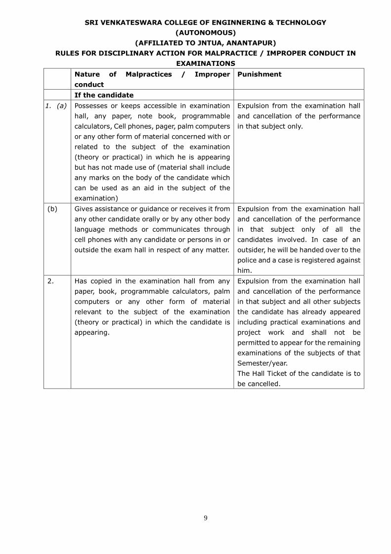
RULES FOR DISCIPLINARY ACTION FOR MALPRACTICE / IMPROPER CONDUCT IN
EXAMINATIONS
Nature of Malpractices / Improper
conduct
Punishment
If the candidate
1. (a) Possesses or keeps accessible in examination
hall, any paper, note book, programmable
calculators, Cell phones, pager, palm computers
or any other form of material concerned with or
related to the subject of the examination
(theory or practical) in which he is appearing
but has not made use of (material shall include
any marks on the body of the candidate which
can be used as an aid in the subject of the
examination)
Expulsion from the examination hall
and cancellation of the performance
in that subject only.
(b) Gives assistance or guidance or receives it from
any other candidate orally or by any other body
language methods or communicates through
cell phones with any candidate or persons in or
outside the exam hall in respect of any matter.
Expulsion from the examination hall
and cancellation of the performance
in that subject only of all the
candidates involved. In case of an
outsider, he will be handed over to the
police and a case is registered against
him.
2. Has copied in the examination hall from any
paper, book, programmable calculators, palm
computers or any other form of material
relevant to the subject of the examination
(theory or practical) in which the candidate is
appearing.
Expulsion from the examination hall
and cancellation of the performance
in that subject and all other subjects
the candidate has already appeared
including practical examinations and
project work and shall not be
permitted to appear for the remaining
examinations of the subjects of that
Semester/year.
The Hall Ticket of the candidate is to
be cancelled.
10
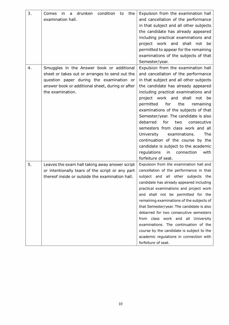
3. Comes in a drunken condition to the
examination hall.
Expulsion from the examination hall
and cancellation of the performance
in that subject and all other subjects
the candidate has already appeared
including practical examinations and
project work and shall not be
permitted to appear for the remaining
examinations of the subjects of that
Semester/year.
4. Smuggles in the Answer book or additional
sheet or takes out or arranges to send out the
question paper during the examination or
answer book or additional sheet, during or after
the examination.
Expulsion from the examination hall
and cancellation of the performance
in that subject and all other subjects
the candidate has already appeared
including practical examinations and
project work and shall not be
permitted for the remaining
examinations of the subjects of that
Semester/year. The candidate is also
debarred for two consecutive
semesters from class work and all
University examinations. The
continuation of the course by the
candidate is subject to the academic
regulations in connection with
forfeiture of seat.
5. Leaves the exam hall taking away answer script
or intentionally tears of the script or any part
thereof inside or outside the examination hall.
Expulsion from the examination hall and
cancellation of the performance in that
subject and all other subjects the
candidate has already appeared including
practical examinations and project work
and shall not be permitted for the
remaining examinations of the subjects of
that Semester/year. The candidate is also
debarred for two consecutive semesters
from class work and all University
examinations. The continuation of the
course by the candidate is subject to the
academic regulations in connection with
forfeiture of seat.
11
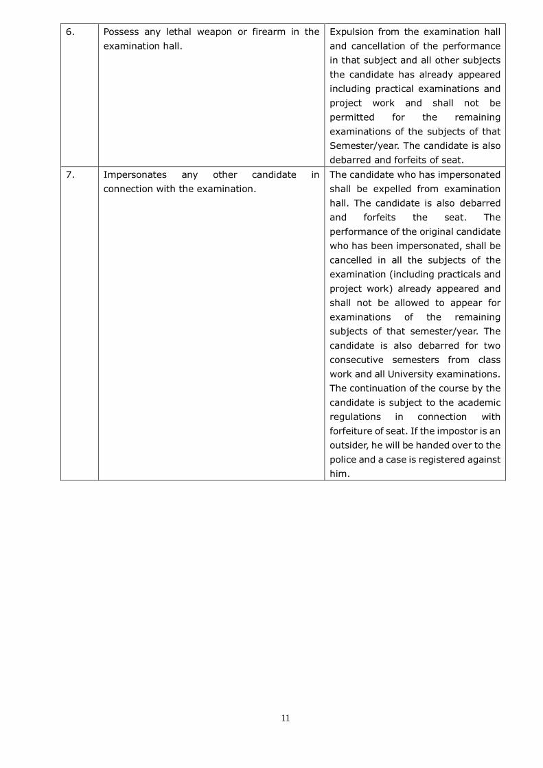
6. Possess any lethal weapon or firearm in the
examination hall.
Expulsion from the examination hall
and cancellation of the performance
in that subject and all other subjects
the candidate has already appeared
including practical examinations and
project work and shall not be
permitted for the remaining
examinations of the subjects of that
Semester/year. The candidate is also
debarred and forfeits of seat.
7. Impersonates any other candidate in
connection with the examination.
The candidate who has impersonated
shall be expelled from examination
hall. The candidate is also debarred
and forfeits the seat. The
performance of the original candidate
who has been impersonated, shall be
cancelled in all the subjects of the
examination (including practicals and
project work) already appeared and
shall not be allowed to appear for
examinations of the remaining
subjects of that semester/year. The
candidate is also debarred for two
consecutive semesters from class
work and all University examinations.
The continuation of the course by the
candidate is subject to the academic
regulations in connection with
forfeiture of seat. If the impostor is an
outsider, he will be handed over to the
police and a case is registered against
him.
12
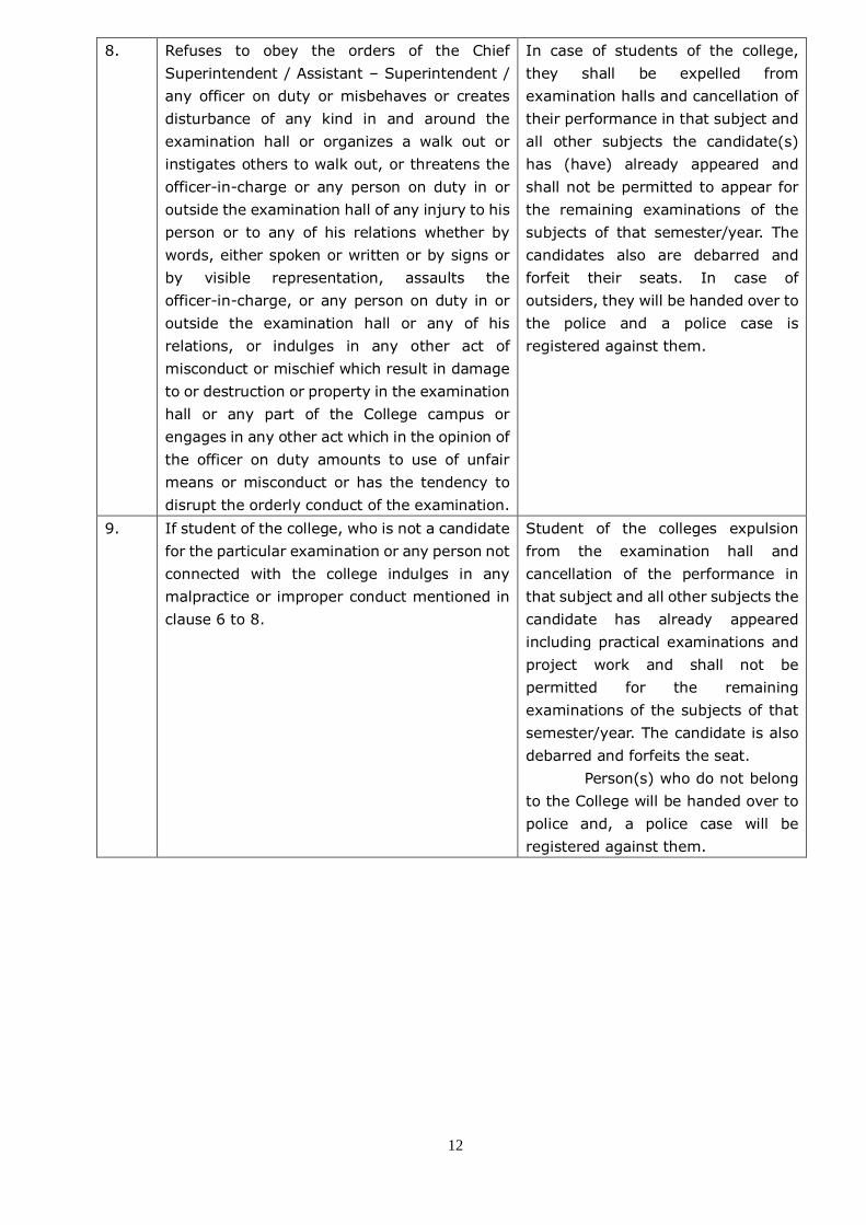
8. Refuses to obey the orders of the Chief
Superintendent / Assistant – Superintendent /
any officer on duty or misbehaves or creates
disturbance of any kind in and around the
examination hall or organizes a walk out or
instigates others to walk out, or threatens the
officer-in-charge or any person on duty in or
outside the examination hall of any injury to his
person or to any of his relations whether by
words, either spoken or written or by signs or
by visible representation, assaults the
officer-in-charge, or any person on duty in or
outside the examination hall or any of his
relations, or indulges in any other act of
misconduct or mischief which result in damage
to or destruction or property in the examination
hall or any part of the College campus or
engages in any other act which in the opinion of
the officer on duty amounts to use of unfair
means or misconduct or has the tendency to
disrupt the orderly conduct of the examination.
In case of students of the college,
they shall be expelled from
examination halls and cancellation of
their performance in that subject and
all other subjects the candidate(s)
has (have) already appeared and
shall not be permitted to appear for
the remaining examinations of the
subjects of that semester/year. The
candidates also are debarred and
forfeit their seats. In case of
outsiders, they will be handed over to
the police and a police case is
registered against them.
9. If student of the college, who is not a candidate
for the particular examination or any person not
connected with the college indulges in any
malpractice or improper conduct mentioned in
clause 6 to 8.
Student of the colleges expulsion
from the examination hall and
cancellation of the performance in
that subject and all other subjects the
candidate has already appeared
including practical examinations and
project work and shall not be
permitted for the remaining
examinations of the subjects of that
semester/year. The candidate is also
debarred and forfeits the seat.
Person(s) who do not belong
to the College will be handed over to
police and, a police case will be
registered against them.
13
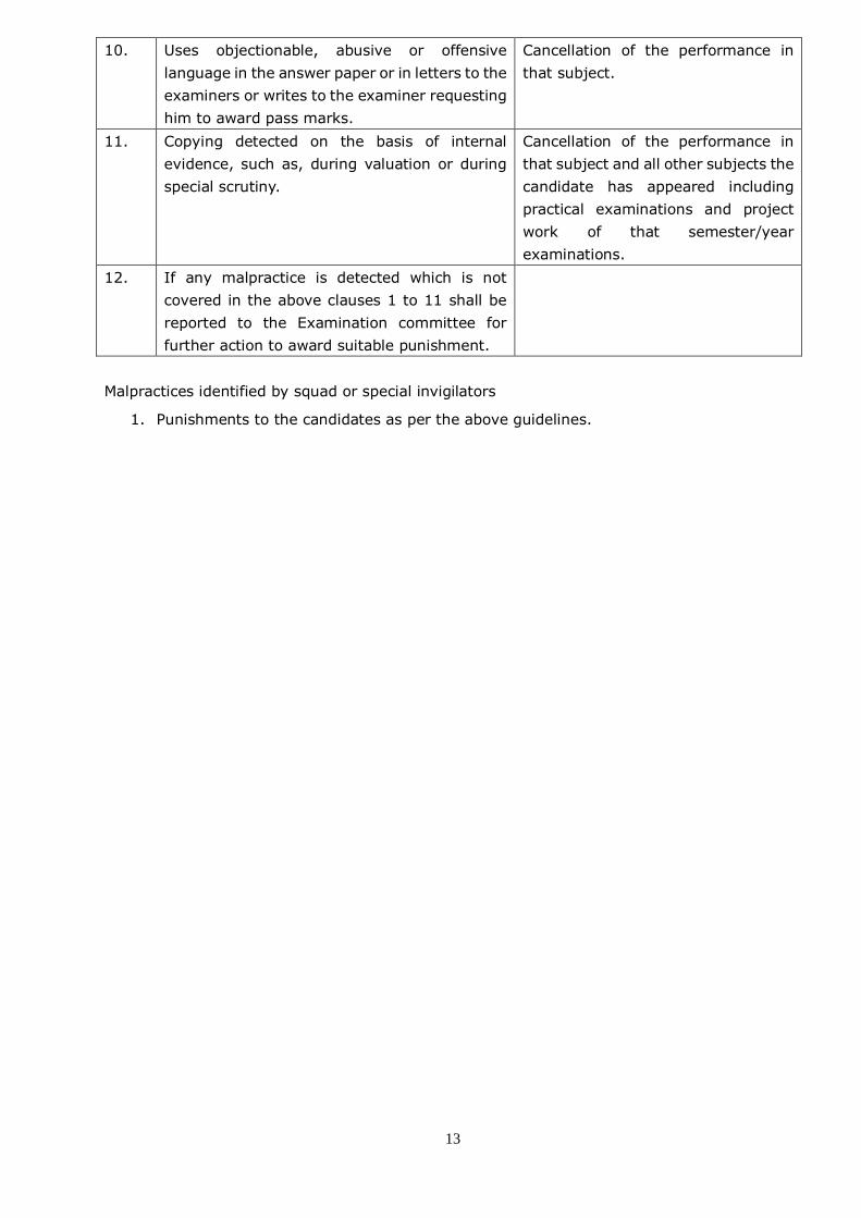
10. Uses objectionable, abusive or offensive
language in the answer paper or in letters to the
examiners or writes to the examiner requesting
him to award pass marks.
Cancellation of the performance in
that subject.
11. Copying detected on the basis of internal
evidence, such as, during valuation or during
special scrutiny.
Cancellation of the performance in
that subject and all other subjects the
candidate has appeared including
practical examinations and project
work of that semester/year
examinations.
12. If any malpractice is detected which is not
covered in the above clauses 1 to 11 shall be
reported to the Examination committee for
further action to award suitable punishment.
Malpractices identified by squad or special invigilators
1. Punishments to the candidates as per the above guidelines.
14
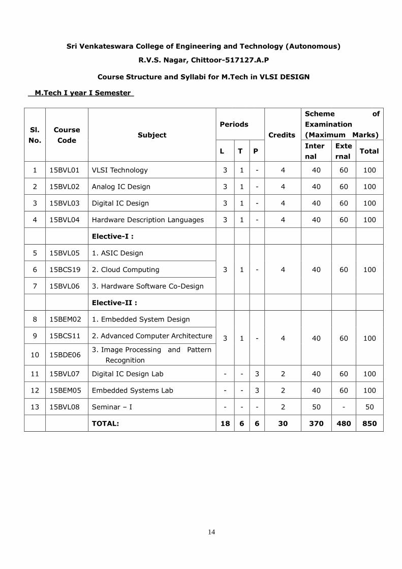
Sri Venkateswara College of Engineering and Technology (Autonomous)
R.V.S. Nagar, Chittoor-517127.A.P
Course Structure and Syllabi for M.Tech in VLSI DESIGN
M.Tech I year I Semester
Sl.
No.
Course
Code Subject
Periods
Credits
Scheme of
Examination
(Maximum Marks)
L T P Inter
nal
Exte
rnal Total
1 15BVL01 VLSI Technology 3 1 - 4 40 60 100
2 15BVL02 Analog IC Design 3 1 - 4 40 60 100
3 15BVL03 Digital IC Design 3 1 - 4 40 60 100
4 15BVL04 Hardware Description Languages 3 1 - 4 40 60 100
Elective-I :
5 15BVL05 1. ASIC Design
3 1 - 4 40 60 100 6 15BCS19 2. Cloud Computing
7 15BVL06 3. Hardware Software Co-Design
Elective-II :
8 15BEM02 1. Embedded System Design
3 1 - 4 40 60 100 9 15BCS11 2. Advanced Computer Architecture
10 15BDE06 3. Image Processing and Pattern
Recognition
11 15BVL07 Digital IC Design Lab - - 3 2 40 60 100
12 15BEM05 Embedded Systems Lab - - 3 2 40 60 100
13 15BVL08 Seminar – I - - - 2 50 - 50
TOTAL: 18 6 6 30 370 480 850
15
M.Tech I Year II Semester
Sl.
No.
Course
Code Subject
Periods Credits
Scheme of Examination
(Maximum Marks)
L T P Internal External Total
1 15BVL09 FPGA Architectures &
Applications 3 1
- 4 40 60 100
2 15BVL10 Low Power VLSI Design 3 1
- 4 40 60 100
3 15BVL11 Algorithms for VLSI Design
Automation 3 1
- 4 40 60 100
4 15BVL12 Testing & Testability 3 1
- 4 40 60 100
Elective-III:
5 15BVL13 1. Nano Electronics
3 1
- 4 40 60 100 6 15BCS10
2. Cryptography and Network
Security
7 15BSE19 3. Scripting Language for
VLSI Design Automation
Elective-IV:
8 15BDE11 1. DSP Processors &
Architectures
3 1 - 4 40 60 100 9 15BDE15 2. High Speed Networks
10 15BVL14 3. Electronic Design
Automation Tools
11 15BVL15 Mixed Signal Lab - - 3 2 40 60 100
12 15BDE18 Advanced DSP Lab - - 3 2 40 60 100
13 15BVL16 Seminar-II - - - 2 50 - 50
14 15BVL17 Comprehensive viva - - - 2 100 - 100
TOTAL: 18 6 4 32 470 480 950
M.Tech II Year III & IV Semesters
Sl.
No.
Course
Code Subject
Periods Credits
Scheme of Examination
(Maximum Marks)
L T P Internal External Total
1 15BVL18 Project Work - - - 12 120 180 300
16
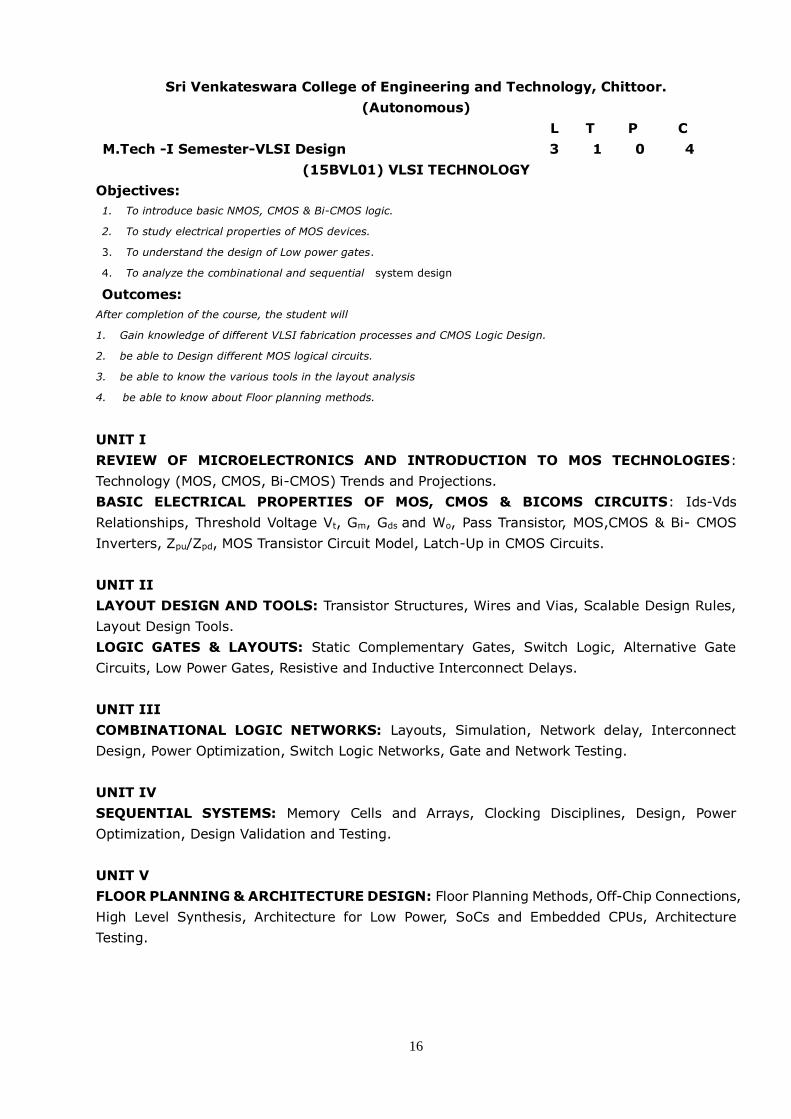
Sri Venkateswara College of Engineering and Technology, Chittoor.
(Autonomous)
L T P C
M.Tech -I Semester-VLSI Design 3 1 0 4
(15BVL01) VLSI TECHNOLOGY
Objectives:
1. To introduce basic NMOS, CMOS & Bi-CMOS logic.
2. To study electrical properties of MOS devices.
3. To understand the design of Low power gates.
4. To analyze the combinational and sequential system design
Outcomes:
After completion of the course, the student will
1. Gain knowledge of different VLSI fabrication processes and CMOS Logic Design.
2. be able to Design different MOS logical circuits.
3. be able to know the various tools in the layout analysis
4. be able to know about Floor planning methods.
UNIT I
REVIEW OF MICROELECTRONICS AND INTRODUCTION TO MOS TECHNOLOGIES:
Technology (MOS, CMOS, Bi-CMOS) Trends and Projections.
BASIC ELECTRICAL PROPERTIES OF MOS, CMOS & BICOMS CIRCUITS: Ids-Vds
Relationships, Threshold Voltage Vt, Gm, Gds and Wo, Pass Transistor, MOS,CMOS & Bi- CMOS
Inverters, Zpu/Zpd, MOS Transistor Circuit Model, Latch-Up in CMOS Circuits.
UNIT II
LAYOUT DESIGN AND TOOLS: Transistor Structures, Wires and Vias, Scalable Design Rules,
Layout Design Tools.
LOGIC GATES & LAYOUTS: Static Complementary Gates, Switch Logic, Alternative Gate
Circuits, Low Power Gates, Resistive and Inductive Interconnect Delays.
UNIT III
COMBINATIONAL LOGIC NETWORKS: Layouts, Simulation, Network delay, Interconnect
Design, Power Optimization, Switch Logic Networks, Gate and Network Testing.
UNIT IV
SEQUENTIAL SYSTEMS: Memory Cells and Arrays, Clocking Disciplines, Design, Power
Optimization, Design Validation and Testing.
UNIT V
FLOOR PLANNING & ARCHITECTURE DESIGN: Floor Planning Methods, Off-Chip Connections,
High Level Synthesis, Architecture for Low Power, SoCs and Embedded CPUs, Architecture
Testing.
17
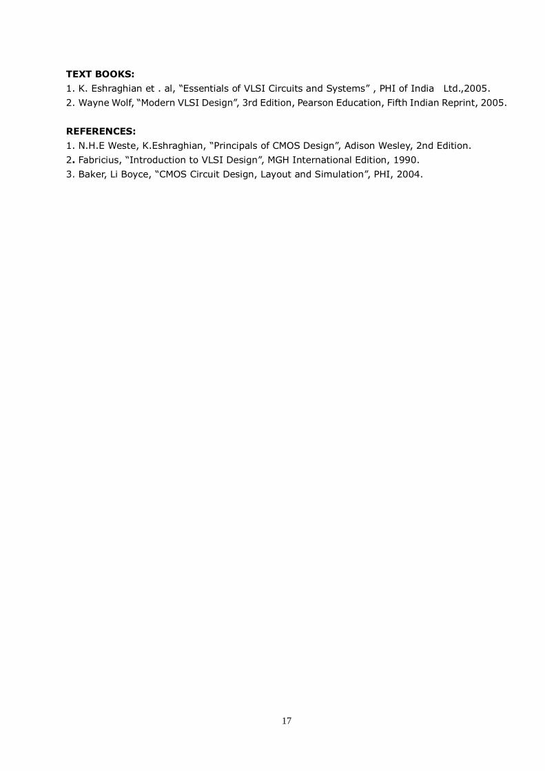
TEXT BOOKS:
1. K. Eshraghian et . al, “Essentials of VLSI Circuits and Systems” , PHI of India Ltd.,2005.
2. Wayne Wolf, “Modern VLSI Design”, 3rd Edition, Pearson Education, Fifth Indian Reprint, 2005.
REFERENCES:
1. N.H.E Weste, K.Eshraghian, “Principals of CMOS Design”, Adison Wesley, 2nd Edition.
2. Fabricius, “Introduction to VLSI Design”, MGH International Edition, 1990.
3. Baker, Li Boyce, “CMOS Circuit Design, Layout and Simulation”, PHI, 2004.
18
Sri Venkateswara College of Engineering and Technology, Chittoor.
(Autonomous)
L T P C
M.Tech- I Semester-VLSI Design 3 1 0 4
(15BVL02) ANALOG IC DESIGN
Objectives:
To enable the students
1. To understand the fundamentals of MOS transistor and it’s modeling.
2. To understand the design and compensating techniques for a operational amplifier.
3. To understand the operation of sample and hold circuits.
4. To understand the operation of data converters.
Outcomes:
The student will
1. Gain knowledge of different Interpolating, Folding and Pipelining techniques.
2. be able to Design different Sample and Hold Switched Capacitor Circuits.
3. be analyze the various CMOS various operational amplifiers
4. be able to know about operation of data converters.
UNIT I
MOS TRANSISTORS, MODELLING AND CURRENT MIRROR:
MOS Transistors- Modeling in Linear and Saturation Regions, Advanced MOS Modeling, Simple
CMOS Current Mirror, Common-Source Amplifier, Source-Follower or Common-Drain Amplifier,
Common-Gate Amplifier, Source-Degenerated Current Mirrors, Cascade Current Mirrors and
Cascade Gain Stage.
UNIT II
OPERATIONAL AMPLIFIER DESIGN, COMPENSATION AND COMPARATORS: Two-Stage
CMOS Opamp, Opamp Compensation, Advanced Current Mirrors, Folded-Cascade Opamp,
Current Mirror Opamp, Fully Differential Opamps, Common-Mode Feedback Circuits. Comparator
Specifications, Charge-Injection Errors, Latched Comparators and Examples of CMOS and
Bi-CMOS Comparators.
UNIT III
SAMPLE AND HOLDS AND SWITCHED CAPACITOR CIRCUITS: Performance of
Sample-and-Hold Circuits, MOS Sample-and-Hold Basics, Examples of CMOS S/H Circuits,
Bipolar and Bi-CMOS Sample and Holds.
Switched Capacitor Circuits: Basic Building Blocks, Basic Operation and Analysis, Noise in
Switched-Capacitor Circuits, First-Order Filters, Biquad Filters, Charge Injection and
Switched-Capacitor Gain Circuits.
UNIT IV
DATA CONVERTERS: Quantization Noise, Signed Codes, Decoder-Based D/A Converters,
Binary-Scaled D/A Converters, Thermometer-Code D/A Converters and Hybrid D/A Converters
Successive-Approximation A/D Converters, Algorithmic (or Cyclic) A/D Converter, Pipelined A/D
Converters, Flash Converters, Two-Step A/D Converters, Interpolating A/D Converters and
Folding A/D Converters.
19
UNIT V
OVERSAMPLING CONVERTERS AND FILTERS: Oversampling without Noise Shaping,
Oversampling with Noise Shaping, System Architectures, Digital Decimation Filters, Higher-Order
Modulators, Bandpass Oversampling Converters and Practical Considerations. .
TEXT BOOKS:
1. Tony Chan Carusone, David A. Johns & Ken Martin, “Analog Integrated Circuit Design”, 2nd
Edition, John Wiley, 2012.
2. Behzad Razavi, “Design of Analog CMOS Integrated Circuit” Tata-Mc GrawHill, 2006.
REFERENCES:
1. Philip Allen & Douglas Holberg, “CMOS Analog Circuit Design”, Oxford University Press, 2006.
2. Gregolian & Temes, “Analog MOS Integrated Circuits”, John Wiley, 2004.
20
Sri Venkateswara College of Engineering and Technology, Chittoor.
(Autonomous)
L T P C
M.Tech- I Semester-VLSI Design 3 1 0 4
(15BVL03) DIGITAL IC DESIGN
Objectives:
1. To analyze static and dynamic characteristics of CMOS inverter.
2. To understand the sizing of transistors to optimize performance or power.
3. To analyze and design of SRAM and DRAM.
4. To design sub system components.
Outcomes:
After completion of the course, the student will be able to:
1. Gain knowledge On Layout Design Rules.
2. Solve problems in the design of CMOS logic circuits, with reference to speed and power Consumption.
3. Analyze the static and dynamic characteristics of BICMOS circuits.
4. Design the fundamental blocks of VLSI circuits, both by circuit schematic and physical layout.
UNIT I
CMOS Inverters - Static and Dynamic Characteristics, Static and Dynamic CMOS Design - Domino
and NOR Logic - Combinational and Sequential Circuits.
UNIT II
Method of Logical Effort for Transistor Sizing, Power Consumption in CMOS Gates, Arithmetic
Circuits in CMOS VLSI – Adders, Multipliers, Shifter.
UNIT III
CMOS Memory Design - SRAM and DRAM, Bipolar Gate Design - BiCMOS Logic - Static and
Dynamic Behavior, Delay and Power Consumption in BiCMOS Logic.
UNIT IV
Layout Design Rules: Need for Design Rules, Mead Conway Design Rules for the Silicon Gate
NMOS Process, CMOS Based Design Rules, Simple Layout Examples, Sheet Resistance, Area
Capacitance, Wire Capacitance, Drive Large Capacitive Load.
UNIT V
Subsystem Design Process: General arrangement of 4-bit Arithmetic Processor, Design of 4-Bit
Shifter, Design of ALU sub-system, Implementing ALU functions with an Adder, Carry-Look-Ahead
Adders, Multipliers, Serial Parallel Multipliers, Pipeline Multiplier Array, Modified Booth’s
Algorithm.
21
TEXT BOOKS:
1. Jan M Rabaey, “Digital Integrated Circuits - A Design Perspective”, Prentice Hall, 1997.
2. Sung-Mo Kang & Yusuf Leblebici, “CMOS Digital Integrated Circuits - Analysis &
Design”, MGH, Second Ed., 1999.
3. Douglas A. Pucknell and Kamran Eshraghian, “Basic VLSI Design”, PHI, 2013.
REFERENCES:
1. Ken Martin, “Digital Integrated Circuit Design”, Oxford University Press, 2000.
2. Neil H E West and Kamran Eshranghian, ”Principles of CMOS VLSI Design: A System
Perspective”, Addision-Wesley 2nd Edition,2002.
3. R. J. Baker, H. W. Li, and D. E. Boyce, “CMOS circuit design, layout, and simulation”. New York:
IEEE Press, 1998.
22
Sri Venkateswara College of Engineering and Technology, Chittoor.
(Autonomous)
L T P C
M.Tech- I Semester-VLSI Design 3 1 0 4
(15BVL04) HARDWARE DESCRIPTION LANGUAGES
Objectives:
1. To understand various modeling in HDL.
2. To design digital circuits using verilog HDL.
3. To understand verilog data types , operators in verilog HDL.
4. To understand synthesis in verilog HDL.
Outcomes:
After completion of the course, the student will be able to:
1. Analyze the various design methodologies in HDL.
2. Program in verilog HDL for digital circuits.
3. Analyze the synthesis of digital circuits.
4. Design the digital circuits in verilog HDL.
UNIT I
HARDWARE MODELING WITH THE VERILOG HDL : Hardware Encapsulation, Verilog Module,
Hardware Modeling Verilog Primitives, Descriptive Styles, Structural Connections, Behavioral
Description In Verilog, Hierarchical Descriptions of Hardware, Structured (Top Down) Design
Methodology, Arrays of Instances, Using Verilog for Synthesis, Language Conventions,
Representation of Numbers.
UNIT II
LOGIC SYSTEM, DATA TYPES AND OPERATORS FOR MODELING IN VERILOG HDL:
User-Defined Primitives, Combinational Behavior User-Defined Primitives, Sequential Behavior
User-Defined Primitives, Initialization of Sequential Primitives. Verilog Variables, Logic Value Set,
Data Types, Strings. Constants, Operators, Expressions and Operands, Operator Precedence
Models of Propagation Delay, Built-In Constructs for Delay, Signal Transitions, Verilog Models for
Gate Propagation Delay (Inertial Delay), Time Scales for Simulation, Verilog Models for Net Delay
(Transport Delay), Module Paths and Delays, Path Delays and Simulation, Inertial Delay Effects
and Pulse Rejection.
UNIT III
BEHAVIORAL DESCRIPTIONS IN VERILOG HDL: Verilog Behaviors, Behavioral Statements,
Procedural Assignment, Procedural Continuous Assignments, Procedural Timing Controls and
Synchronization, Intra-Assignment, Delay-Blocked Assignments, Non-Blocking Assignment,
Intra-Assignment Delay: Non-Blocking Assignment, Simulation of Simultaneous Procedural
Assignments, Repeated Intra Assignment Delay, Indeterminate Assignments and Ambiguity,
Constructs for Activity Flow Control, Tasks and Functions, Summary of Delay Constructs in Verilog,
System Tasks for Timing Checks, Variable Scope Revisited, Module Contents, Behavioral Models
of Finite State Machines.
23
UNIT IV
SYNTHESIS OF COMBINATIONAL LOGIC: HDL-Based Synthesis, Technology-Independent
Design, Benefits of Synthesis, Synthesis Methodology, Vendor Support, Styles for Synthesis of
Combinational Logic, Technology Mapping and Shared Resources, Three State Buffers, Three
State Outputs and Don’t Cares, Synthesis of Sequential Logic Synthesis of Sequential Udps,
Synthesis of Latches, Synthesis of Edge-Triggered Flip Flops, Registered Combinational Logic,
Shift Registers and Counters, Synthesis of Finite State Machines, Resets, Synthesis of Gated
Clocks, Design Partitions and Hierarchical Structures.
SYNTHESIS OF LANGUAGE CONSTRUCTS: Synthesis of Nets, Synthesis of Register Variables,
Restrictions on Synthesis of “X” and “Z”, Synthesis of Expressions and Operators, Synthesis of
Assignments, Synthesis of Case and Conditional Statement, Synthesis of Resets, Timings
Controls in Synthesis, Synthesis of Multi-Cycle Operations, Synthesis of Loops, Synthesis if Fork
Join Blocks, Synthesis of The Disable Statement Synthesis of User-Defined Tasks, Synthesis of
User-Defined Functions, Synthesis of Specify Blocks, Synthesis of Compiler Directives.
UNIT V
SWITCH-LEVEL MODELS IN VERILOG: MOS Transistor Technology, Switch Level Models of
MOS Transistors, Switch Level Models of Static CMOS Circuits, Alternative Loads and Pull Gates,
CMOS Transmission Gates. Bio-Directional Gates (Switches), Signal Strengths, Ambiguous
Signals, Strength Reduction By Primitives, Combination and Resolution of Signal Strengths,
Signal Strengths and Wired Logic, Design Examples in Verilog.
TEXT BOOKS:
1. M.D.Ciletti, “Modeling, Synthesis and Rapid Prototyping with the Verilog HDL”, Prentice-Hall,
1999.
2. Z.Nawabi, “VHDL Analysis and Modeling of Digital Systems”, (2/E), McGraw Hill, 1998.
REFERENCES:
1. M.G.Arnold, “Verilog Digital – Computer Design”, Prentice-Hall (PTR), 1999.
2. Perry, “VHDL”, (3/E), McGraw Hill.
24
Sri Venkateswara College of Engineering and Technology, Chittoor.
(Autonomous)
M.Tech- I Semester-VLSI Design L T P C
3 1 0 4
(15BVL05) ASIC DESIGN
(ELECTIVE-I)
Objectives:
1. To Impart fundamental knowledge of ASICs - Design Styles
2. To make the students familiar with the various design techniques
3. To give enough exposure to the logic synthesis, simulation and testing.
4. To learn about routing and partitioning.
Outcomes:-
The Student will be
1. Gain knowledge on the basics of ASIC design styles and FPGA.
2. able to understand Design flow and methodologies.
3. Familiar with the various design aspects, logic synthesis, simulation and testing.
4. learn XILINX, ALTERA tools.
UNIT I
ASICs - DESIGN STYLES: Introduction, Categories, Gate Arrays, Standard Cells, Cell Based
ASICs, Mixed Mode and Analogue ASICs, PLDs.
ASICs – PROGRAMMABLE LOGIC DEVICES: Overview, PAL based PLDS Structures, PAL
Characteristics, FPGAS: Introduction, Selected Families, Design Outline.
UNIT II
ASICs – DESIGN ISSUES: Design Methodologies and Design Tools, Design for Testability,
Economies.
ASICs - CHARACTERISTICS AND PERFORMANCE: Design Styles, Gate Arrays, Standard Cell
based ASICS, Mixed Mode and Analogue ASICs.
UNIT III
ASICs-DESIGN TECHNIQUES: Overview- Design Flow and Methodology, Hardware Description
Languages, Simulation and Checking, Commercial Design Tools, FPGA Design Tools: XILINX,
ALTERA
UNIT IV
LOGIC SYNTHESIS, SIMULATION AND TESTING: Verilog and Logic Synthesis -VHDL and
Logic Synthesis, Types of Simulation, Boundary Scan Test, Fault Simulation, Automatic Test
Pattern Generation.
UNIT V
ASIC CONSTRUCTION: Floor Planning, Placement and Routing, System Partition.
FPGA PARTITIONING: Partitioning Methods, Floor Planning, Placement, Physical Design Flow,
Global Routing, Detailed Routing, Special Routing, Circuit Extraction, DRC.
25
TEXT BOOKS:
1. L.J. Herbst, “Integrated Circuit Engineering”, OXFORD SCIENCE Publications, 1996.
2. K. Eshraghian et . al, “Essentials of VLSI Circuits and Systems”, PHI of India Ltd.,2005
3. Wayne Wolf, “Modern VLSI Design”, Pearson Education, Fifth Indian Reprint, 3rd Edition,
2005.
References:
1. M.J.S.Smith, “Application - Specific Integrated Circuits”, Addison-Wesley Longman Inc
1997.
2. Douglas A Pucknell, Weste, K.Eshraghian, “Basic VLSI Design”, PHI, 3rd Edition.
3. Fabricius, “Introduction to VLSI Design”, MGH International Edition, 1990.
26
Sri Venkateswara College of Engineering and Technology, Chittoor.
(Autonomous)
L T P C
M.Tech- I Semester-VLSI Design 3 1 0 4
(15BCS19) CLOUD COMPUTING
(ELECTIVE-I)
Objectives:
The Objective of this course is to make students to
1 Learn fundamental ideas behind Cloud Computing, the evolution of the paradigm, its applicability; benefits, as
well as current and future challenges;
2 Learn about cloud storage technologies and relevant distributed file systems;
3 Understand the emerging area of "cloud computing" and how it relates to traditional models of computing.
4 Gain competence in MapReduce as a programming model for distributed processing of large datasets.
Outcomes:
At the end of course student should be able to
1 Articulate the main concepts, key technologies, strengths, and limitations of cloud computing and the
possible applications for state-of-the-art cloud computing
2 Identify the architecture and infrastructure of cloud computing, including SaaS, PaaS, IaaS, public cloud, private
cloud, hybrid cloud, etc.
3 Explain the core issues of cloud computing such as security, privacy, and interoperability.
4 Choose the appropriate technologies, algorithms, and approaches for the related issues.
UNIT I
OVERVIEW OF CLOUD COMPUTING: Meaning of the terms Cloud and Cloud Computing, Cloud
Based Service Offerings, Grid Computing Vs Cloud Computing, Benefits of Cloud Model,
Limitations, Legal Issues, Key Characteristics of Cloud Computing, Challenges for the Cloud,
Evolution of Cloud Computing.
UNIT II
WEB SERVICES DELIVERED FROM THE CLOUD: Infrastructure as a Service,
Platform-as-a-Service, Software-as-a-Service, Building Cloud Networks: Evolution from the MSP
Model to Cloud Computing and Software-as-a-Service, Cloud Data Center, SOA as Step toward
Cloud Computing, Basic approach to a Data Center based SOA.
UNIT III
FEDERATION PRESENCE, IDENTITY AND PRIVACY IN THE CLOUD: Federation in the Cloud,
Presence in the Cloud, Privacy and its relation to Cloud based Information System, Security in the
Cloud: Cloud Security Challenges, Software-as-a-service Security, Common Standards in Cloud
computing: Open Cloud Consortium, Distributed Management Task Force, Standards for
Application Developers, Standards for Messaging, Standards for Security.
27
UNIT IV
END USER ACCESS TO CLOUD COMPUTING: Youtube, Zimbra, Facebook, Zoho, Dimdim
Collaboration Mobile Internet Devices and the Cloud: Smartphone, Mobile Operating Systems for
Smart Phones, Mobile Platform Virtualization, Collaboration Applications for Mobile Platforms,
Future Trends.
UNIT V
VIRTUALIZATION: Adding Guest Operating System, Cloud Computing, Downloading Open
Solaris as a Guest OS, Using 7-Zip Archive Tool Casestudies1: Amazon EC2, Amazon Simple DB:
Google App Engine.
TEXT BOOKS:
1. John W. Rittinghouse, James F. Ransome ,“Cloud Computing implementation, management
and security”, CRC Press, Taylor & Francis group, 2010.
2. Anthony T.velte, TobJ.velte Robert Elsenpeter, “Cloud Computing: A practical approach”, Tata
McGraw Hill edition, 2010.
REFERENCES:
1. George Reese, Cloud Application Architectures Building Applications and Infrastructure in the
Cloud, O’Reilly Media Released, April 2009.
2. David S. Linthicum ,”Cloud Computing and SOA convergence in your enterprise”, Addison-
Wesley.
28
Sri Venkateswara College of Engineering and Technology, Chittoor.
(Autonomous)
L T P C
M.Tech- I Semester- VLSI Design 3 1 0 4
(15BVL06) HARDWARE SOFTWARE CO - DESIGN
(ELECTIVE-I)
Objectives:
1. To introduce the hardware/software code sign to the practicing design
2. Provides key code sign concepts and attempts to show the benefits of the code sign approach over the current
design process.
3. Fundamentals, the Design Space of Custom Architectures, the Hardware/software Interface and Application
Examples.
4. Techniques are used to partition a system into hardware and software components
Outcomes:
After completion of course, the students will be able to
1. Design environment that helps the reader to perform experiments in hardware/software code sign.
2. partition a system into hardware and software components by using techniques
3. to understand various system level specifications
4. understand design Issues, Trends, and Considerations
UNIT I
CO-DESIGN ISSUES: Co- Design Models, Architectures, Languages, a Generic Co-design
Methodology.
CO-SYNTHESIS ALGORITHMS: Hardware Software Synthesis Algorithms: Hardware- Software
Partitioning, Distributed System Co-Synthesis.
UNIT II
PROTOTYPING AND EMULATION: Prototyping and Emulation Techniques, Prototyping and
Emulation Environments, Future Developments in Emulation and Prototyping.
TARGET ARCHITECTURES: Architecture Specialization Techniques, System Communication
Infrastructure, Target Architecture and Application System Classes, Architecture for Control
Dominated Systems (8051-Architectures for High Performance Control), Architecture for Data
Dominated Systems (ADSP21060, TMS320C60), Mixed Systems.
UNIT III
COMPILATION TECHNIQUES AND TOOLS FOR EMBEDDED PROCESSOR
ARCHITECTURES: Modern Embedded Architectures, Embedded Software Development Needs,
Compilation Technologies, Practical Consideration in a Compiler Development Environment.
UNIT IV
DESIGN SPECIFICATION AND VERIFICATION: Design, Co-Design, the Co-Design
Computational Model, Concurrency Coordinating Concurrent Computations, Interfacing
Components, Design Verification, Implementation Verification, Verification Tools and Interface
Verification
29
UNIT V
LANGUAGES FOR SYSTEM- LEVEL SPECIFICATION AND DESIGN-I: System – Level
Specification, Design Representation for System Level Synthesis, System Level Specification
Languages,
LANGUAGES FOR SYSTEM-LEVEL SPECIFICATION AND DESIGN-II: Heterogeneous
Specifications and Multi Language Co-Simulation, the Cosyma System and Lycos System.
TEXT BOOKS:
1. Jorgen Staunstrup, Wayne Wolf,“Hardware / Software Co- Design Principles and Practice”,
2009, Springer.
2. Kluwer , “Hardware / Software Co- Design Principles and Practice”, 2002, Academic Publishers.
REFERENCE BOOK:
1. Patrick R. Schaumont, “A Practical Introduction to Hardware/Software Co-design”, 2010,
Springer.
2. Giovanni, Wayne Wolf, “Readings in Hardware Software Co – design”, Academic Press, 2002.
30
Sri Venkateswara College of Engineering and Technology, Chittoor.
(Autonomous)
L T P C
M.Tech- I Semester-VLSI Design 3 1 0 4
(15BEM02) EMBEDDED SYSTEM DESIGN
(ELECTIVE-II)
Objectives:
1.To study the overview of embedded system.
2.To know various communication interfacings.
3.To study the scheduling architectures
4.To study the ARM and SHARC processor.
Outcomes:
After the completion of the course,the students will able :
1. to perform system analysis and architecture design
2. to apply embedded concepts on real time applications
3. to get knowledge on ARM processor and SHARC processor
4. to get an idea about Debugging techniques
UNIT I
INTRODUCTION: Embedded System Overview, Embedded Hardware Units, Embedded
Software in a System, Embedded System on Chip (SoC), Design Process, Classification of
Embedded Systems.
EMBEDDED COMPUTING PLATFORM: CPU Bus, Memory Devices, Component Interfacing,
Networks for Embedded Systems, Communication Interfacings: RS232/UART, RS422/RS485,
IEEE 488 Bus.
UNIT II
SURVEY OF SOFTWARE ARCHITECTURE: Round Robin, Round Robin with Interrupts, Function
Queue Scheduling Architecture, Selecting an Architecture Saving Memory Space.
EMBEDDED SOFTWARE DEVELOPMENT TOOLS: Host and Target Machines, Linkers,
Locations for Embedded Software, Getting Embedded Software into Target System, Debugging
Technique.
UNIT III
RTOS CONCEPTS: Architecture of the Kernel, Interrupt Service Routines, Semaphores, Message
Queues, Pipes.
UNIT IV
INSTRUCTION SETS; Introduction, Preliminaries, ARM Processor, SHARC Processor.
UNIT V
SYSTEM DESIGN TECHNIQUES: Design Methodologies, Requirement Analysis, Specifications,
System Analysis and Architecture Design.
DESIGN EXAMPLES: Telephone PBX, Ink Jet Printer, Water Tank Monitoring System, GPRS,
Personal Digital Assistants, Set Top boxes.
31
TEXT BOOKS:
1.Wayne Wolf, “Computers as a Component: Principles of Embedded Computing System Design”,
2nd Edition, 1998.
2. David E, Simon, “ An Embedded Software”, Premier
3. KVKK Prasad, “Embedded / Real Time Systems”, Dreamtech Press, 2005
REFERENCES:
1. Sri Ram V Iyer, Pankaj Gupta, “Embedded Real Time Systems Programming”, TMH, 2004
2. Frank Vahid, Tony D.Givargis, “Embedded System Design- A Unified Hardware/Software
Introduction”, John Willey, 2002.
32
Sri Venkateswara College of Engineering and Technology, Chittoor.
(Autonomous) L T P C
M.Tech- I Semester- VLSI Design 3 1 0 4
(15BCS11) ADVANCED COMPUTER ARCHITECTURE
(ELECTIVE-II)
Objectives:
The objective of this course is to make students to:
1. Understand memory system organization and architecture, system connection, memory, input/output,
instruction sets, CPU structure and functions and the control Unit operation.
2. To provide in-depth coverage of current and emerging trends in computer architectures, focusing on
performance and the hardware/software interface.
3. Acquire the knowledge of computer organization and architecture (logical design) and relates this to
contemporary design issues
4. Acquire the knowledge of machine level representation of data, assembly level organization
Outcomes:
At the end of the course the student will be able to:
1. know memory hierarchy and its impact on computer cost/ performance.
2. Obtain technical knowhow of the advantage of instruction level parallelism and pipelining for high performance
processor design.
3. Design key features of advanced processing and memory systems.
4. Develop solutions to computing problems using alternative architectures.
UNIT I
FUNDAMENTALS OF COMPUTER DESIGN: Technology Trends, Cost Measuring and
Reporting Performance Quantitative Principles of Computer Design.
UNIT II
INSTRUCTION SET PRINCIPLES AND EXAMPLES: Classifying Instruction Set, Memory
Addressing, Type and Size of Operands, Addressing Modes f or Signal Processing, Operations in
t h e Instruction Set- Instructions f or Control Flow- Encoding an Instruction Set, Role of Compiler.
UNIT III
INSTRUCTION LEVEL PARALLELISM (ILP): Overc oming Data Hazards, Reducing Branch
Costs, High Performance Instruction Delivery, Hardware Based Speculation, Limitation of ILP.
ILP SOFTWARE APPROACH: Compiler Techniques, Static Branch Protection, VLIW Approach,
H/W support for more ILP at compile time, H/W versus S/W solutions.
UNIT IV
MEMORY HIERARCHY DESIGN: Cache Performance, Reducing Cache Misses
Penalty and Miss Rate, Virtual Memory, Protection and examples of VM.
STORAGE SYSTEMS: Types, Buses, RAID, Errors and Failures, Bench Marking, a Storage Device,
Designing an I/O System.
33
UNIT V
MULTIPROCESSORS AND THREAD LEVEL PARALLELISM: Symmetric Shared Memory
Architectures, Distributed Shared Memory, Synchronization, Multi Threading.
INTER CONNECTION NETWORKS AND CLUSTERS: Interconnection Network Media, Practical
i ssues in Interconnecting Networks, Examples, Clusters, Designing a Cluster.
TEXT BOOK:
1. John. Hennessy & David A. Patterson Morgan Kufmann, “Computer Architecture a Quantitative
Approach”, 3rd
edition (An Imprint of Elsevier)
REFERENCES:
1. Kai Hwang and A. Briggs, “Computer Architecture and Parallel Processing”, International Edition
McGraw-Hill.
2. Dezso Sima, Terence Fountain, Peter Kacsuk, “Advanced Computer Architectures”, Pearson
Edition, 2007.
34
Sri Venkateswara College of Engineering and Technology, Chittoor.
(Autonomous)
L T P C
M.Tech-I Semester- VLSI Design 3 1 0 4
(15BDE06) IMAGE PROCESSING AND PATTERN RECOGNITION
(ELECTIVE- II)
Objectives:
1. To understand the general processes of image acquisition, storage, enhancement, segmentation, representation
and description.
2. To implement filtering and enhancement algorithms for monochrome as well as color images.
3. To aware the challenges and understand the principles and applications of visual pattern recognition.
4. To Know various techniques of Image Processing And Pattern Recognition
Outcomes:
At the completion of the course
1. The student will be able to describe and explain the general processes of image acquisition and storage.
2. The student will be able to do enhancement, segmentation, representation, and description.
3. The student will be able to implement filtering and enhancement algorithms for monochrome as well as color
images.
4. The student will learn be able to design and implement visual pattern recognition solutions.
UNIT I
IMAGE REPRESENTATION: Gray Scale and Colour Images, Image Sampling and Quantization.
Two Dimensional Orthogonal Transforms: DFT, WHT, Haar Transform, KLT, DCT.
UNIT II
IMAGE ENHANCEMENT: Filters in Spatial and Frequency Domains, Histogram-Based Processing,
Homomorphic Filtering. Edge Detection, Non Parametric and Model based Approaches, LOG
Filters, Localization Problem.
IMAGE RESTORATION: Degradation Models, PSF, Circulant and Block - Circulant Matrices,
Deconvolution, Restoration using Inverse Filtering, Wiener Filtering and Maximum Entropy based
Methods.
UNIT III
IMAGE SEGMENTATION: Pixel Classification, Bi-Level Thresholding, Multi-Level Thresholding,
P-Tile Method, Adaptive Thresholding, Spectral & Spatial Classification, Edge Detection, Hough
Transform, Region Growing.
FUNDAMENTAL CONCEPTS OF IMAGE COMPRESSION: Compression models, Information
theoretic perspective, Fundamental coding theorem.
UNIT IV
INTRODUCTION: Machine Perception Pattern Recognition Example, Pattern Recognition
Systems, Design Cycle, Learning and Adaption.
BAYESIAN DECISION THEORY: Introduction, Continuous Features, Two Categories
Classifications, Minimum Error Rate Classification, Zone-One Loss Function, Classifiers,
Discriminate Functions and Decision Surfaces.
35
UNIT V
NORMAL DENSITY: Univariate and Multivariate Density, Discriminant Functions For The Normal
Density Different Cases, Bayes Decision Theory – Discrete Features, Compound Bayesian
Decision Theory and Context.
MAXIMUM LIKELIHOOD AND BAYESIAN PARAMETER ESTIMATION: Introduction,
Maximum Likelihood Estimation, Bayesian Estimation, Bayesian Parameter Estimation – Gaussian
Case.
TEXT BOOKS
1.R. C. Gonzalez, R. E. Woods, ”Digital Image Processing”, Pearson Education. 2nd Edition,2002
2. Richard O. Duda, Peter E. hart, David G. Stroke, “Pattern classifications”, Wiley student
Edition, Second Edition.
3. Sergios Theodoridis and Knostantinos koutroumbas, “Pattern Recognition”, Third Edition,
Academic Press.
REFERENCES:
1. S Jayaraman, S Esakkirajan, T Veerakumar, “Digital Image processing”, Tata McGraw Hill
2. R. Jain, R. Kasturi and B.G. Schunck, “Machine Vision”, McGraw-Hill International Edition,
1995
3. Lawerence Rabiner, Biing – Hwang Juang, “Fundamentals of Speech Recognition”, Pearson
Education.
36
Sri Venkateswara College of Engineering and Technology, Chittoor.
(Autonomous)
L T P C
0 0 3 2
M.Tech- I Semester-VLSI Design
(15BVL07) DIGITAL IC DESIGN LAB
Objectives:
1. To Verify of the Functionality of Designed circuits .
2. To synthesize and verify timing synthesis of digital circuits.
3. To verify functionality of various digital circuits.
Outcomes:
After completion of the lab students will be able to:
1. Know the various design methodologies of digital circuits.
2. Know the importance of simulation and synthesis
1. Digital Circuits Description using Verilog and VHDL.
2. Verification of the Functionality of Designed circuits using function Simulator.
3. Timing simulation for critical path time calculation.
4. Synthesis of Digital circuits.
5. Place and Route techniques for major FPGA vendors such as XILINX, ALTERA and ACTEL
etc.
6. Implementation of Designed Digital Circuits using FPGA and CPLD devices.
NOTE: Required Software Tools:
1. Mentor Graphic tools / Cadence tools/ Synopsys tools. (220 nm Technology and Above)
2. Xilinx 9.1i and above for FPGA/CPLDS / FPGA Advantage.
37
Sri Venkateswara College of Engineering and Technology, Chittoor.
(Autonomous)
L T P C
M.Tech- I Semester-VLSI Design 0 0 3 2
(15BEM05) EMBEDDED SYSTEMS LAB
Objectives:
1. To introduce the students to program the 8051 and their interfaces
2. To analyze programs and various devices using KIEL
3. To provide a platform for the students to do multidisciplinary projects
Outcomes:
After completion of the course, the students will able:
1.To perform interfacing using LED &LCD.
2. To perform the program using assembly & C Languages.
3. To perform serial transmission& Reception.
ASSEMBLY:
1. Write a program to
a) Clear the Register
b) Add 3 to Register Ten Times and Place the Result into Memory Use the Indirect Instructions to
Perform Looping.
PROGRAMING IN C:
2. A Door Sensor is connected to RB1 Pin and a Buzzer is connected to RB7. Write a Program to
monitor Door Sensor and when it Open, Sounds the Buzzer by sending a Square Wave of few
Hundred Hz Frequency to it.
3. Write a Program to Toggle all the Bits of PORT B parts continuously with a 250ns Delay.
4. LED’S
(A) Blinking LEDs
(B) Dancing LEDs
5. LCD Interface
6. Serial Communication
A) Serial Transmission
B) Serial Reception
Sri Venkateswara College of Engineering and Technology, Chittoor.
(Autonomous)
L T P C
M.Tech – I Semester – VLSI Design 0 0 0 2
(15BVL08) SEMINAR- I
38
Sri Venkateswara College of Engineering and Technology, Chittoor.
(Autonomous)
L T P C
M.Tech- II Semester- VLSI Design 3 1 0 4
(15BVL09) FPGA ARCHITECTURES & APPLICATIONS
Objectives:
To enable the students
1. To understand different commercially available PLDs, FPGAs.
2. To understand different architectures and routing technology in CPLDs and FPGAs.
3. To understand FSM architectures and systems level design.
4. To familiarize with frontend and backend design tools.
Outcomes:
The student will
1. know about different commercially available FPGA and CPLD architectures.
2. design logic blocks using optimization techniques.
3. Understand the top down design of digital circuits.
4. know about mentor graphics EDA tool.
UNIT I
PROGRAMMABLE LOGIC: ROM, PLA, PAL, PLD, PGA – Features, Programming and Applications
using Complex Programmable Logic Devices ALTERA Series – Max 5000/7000 Series and Altera
FLEX Logic – 10000 Series CPLD, AMD’s – CPLD (Mach 1 To 5); Cypres FLASH 370 Device
Technology, Lattice PLSIs Architectures – 3000 Series – Speed Performance and in System
Programmability.
UNIT II
Field Programmable Gate Arrays – Logic Blocks, Routing Architecture, Design Flow, Technology
Mapping for FPGAs.
CASE STUDIES: XILINX XC4000 & ALTERA’s FLEX 8000/10000 FPGAs: AT & T – ORCA’s
(Optimized Reconfigurable Cell Array): ACTEL’s – ACT-1,2,3 and their Speed Performance.
UNIT III
FINITE STATE MACHINES (FSM): Top Down Design, State Transition Table, State Assignments
for FPGAs, Problem of Initial State Assignment for One Hot Encoding.
REALIZATION OF STATE MACHINE: Charts with a PAL, Alternative Realization for State
Machine Chart using Micro-programming, Linked State Machines. One – Hot State Machine,
Petrinetes for State Machines – Basic Concepts, Properties. Extended Petrinetes for Parallel
Controllers. Finite State Machine – Case Study, Meta Stability, Synchronization.
UNIT IV
FSM ARCHITECTURES AND SYSTEMS LEVEL DESIGN: Architectures Centered around
Non-Registered PLDs, State Machine Designs Centered around Shift Registers, One – Hot Design
Method, Use of ASMs in One – Hot Design, K Application of One – Hot Method, System Level
Design – Controller, Data Path and Functional Partition.
39
UNIT V
DIGITAL FRONT END DIGITAL DESIGN TOOLS FOR FPGAS & ASICS: Using Mentor
Graphics EDA Tool (FPGA Advantage), Design Flow Using FPGAs – Guidelines and Case Studies of
Parallel Adder Cell, Parallel Adder Sequential Circuits, Counters, Multiplexers, Parallel Controllers.
TEXT BOOKS:
1. P.K.Chan & S. Mourad, “Digital Design Using Field Programmable Gate Array”, Prentice Hall ,
1994.
2. Stephen M Trimberger, “Field Programmable Gate Array Technology”, Springer international
Edition, 2007.
3. Stephen D Brown, R.Francis, J.Rose, Z.Vranesic, “Field Programmable Gate Array”, Springer,
1992.
REFERENCES:
1. J. Old Field, R.Dorf, “Field Programmable Gate Arrays”, John Wiley & Sons,2008.
2. Ian Grout, “Digital Systems Design with FPGAs and CPLDs”, Elsevier, Newnes,2008.
40
Sri Venkateswara College of Engineering and Technology, Chittoor.
(Autonomous)
L T P C
M.Tech- II Semester-VLSI Design 3 1 0 4
(15BVL10) LOW POWER VLSI DESIGN
Objectives:
The students will understand
1. the fundamentals of Low power circuit design.
2. the design VTCMOS and MTCMOS circuits.
3. the operation of various adder circuits.
4. the operation of low voltage, low power multiplier circuits.
Outcomes:
The student will be able to
1. know the Low-Power Design Approaches.
2. analyze the Standard Adder Cells, CMOS Adder’s Architectures.
3. understand the operation of Low-Voltage Low-Power Memories.
4. understand the Switched Capacitance Minimization Approaches.
UNIT –I
FUNDAMENTALS: Need for Low Power Circuit Design, Sources of Power Dissipation – Switching
Power Dissipation, Short Circuit Power Dissipation, Leakage Power Dissipation, Glitching Power
Dissipation, Short Channel Effects –Drain induced Barrier Lowering and Punch Through, Surface
Scattering, Velocity Saturation, Impact Ionization, Hot Electron Effect.
UNIT –II
LOW-POWER DESIGN APPROACHES: Low-Power Design through Voltage Scaling – VTCMOS
Circuits, MTCMOS Circuits, Architectural Level Approach –Pipelining and Parallel Processing
Approaches.
SWITCHED CAPACITANCE MINIMIZATION APPROACHES: System Level Measures, Circuit
Level Measures, Mask level Measures.
UNIT –III
LOW-VOLTAGE LOW-POWER ADDERS: Introduction, Standard Adder Cells, CMOS Adder’s
Architectures – Ripple Carry Adders, Carry Look-Ahead Adders, Carry Select Adders, Carry Save
Adders, Low-Voltage Low-Power Design Techniques –Trends of Technology and Power Supply
Voltage, Low-Voltage Low-Power Logic Styles.
UNIT –IV
LOW-VOLTAGE LOW-POWER MULTIPLIERS: Introduction, Overview of Multiplication, Types
of Multiplier Architectures, Braun Multiplier, Baugh- Wooley Multiplier, Booth Multiplier,
Introduction to Wallace Tree Multiplier.
41
UNIT –V
LOW-VOLTAGE LOW-POWER MEMORIES: Basics of ROM, Low-Power ROM Technology, Future
Trend and Development of ROMs, Basics of SRAM, Memory Cell, Pre-charge and Equalization
Circuit, Low-Power SRAM Technologies, Basics of DRAM, Self-Refresh Circuit, Future Trend and
Development of DRAM.
TEXT BOOKS:
1. Sung-Mo Kang, Yusuf Leblebici, “CMOS Digital Integrated Circuits – Analysis and Design”, TMH,
2011.
2. Kiat-Seng Yeo, Kaushik Roy, “Low-Voltage, Low-Power VLSI Subsystems”, TMH Professional
Engineering.
REFERENCE BOOKS:
1. Anantha Chandrakasan, “Low Power CMOS Design”, IEEE Press/Wiley International, 1998.
2. Kaushik Roy, Sharat C. Prasad ,“Low Power CMOS VLSI Circuit Design”, John Wiley & Sons,
2000.
3. Gary K. Yeap, “Practical Low Power Digital VLSI Design”, Kluwer Academic Press, 2002.
42
Sri Venkateswara College of Engineering and Technology, Chittoor.
(Autonomous)
L T P C
M.Tech- II Semester-VLSI Design 3 1 0 4
(15BVL11) ALGORITHMS FOR VLSI DESIGN AUTOMATION
Objectives:
1.To introduce Design methodologies and design automation tools.
2.To understand the different search algorithms on area and speed .
3.To understand the Modeling and simulation methods.
4.To understand physical design automation of FPGA’s and MCM’s
Outcomes:
After completion of the course, the student will
1.Gain knowledge on various design methodologies and design automation tools.
2.Be able to Know the different search algorithms.
3.Be able to know the modeling and simulation.
4.Be able to know the logic synthesis.
UNIT I
PRELIMINARIES: Introduction to Design Methodologies, Design Automation tools,
Algorithmic Graph Theory, Computational Complexity, Tractable and Intractable
problems.
UNIT II
GENERAL PURPOSE METHODS FOR COMBINATIONAL OPTIMIZATION:
Backtracking, Branch and Bound, Dynamic Programming, Integer Linear
Programming, Local Search, Simulated Annealing, Tabu search, Genetic
Algorithms.
UNIT III
LAYOUT AND PLACEMENTS: Layout Compaction, Placement, Floor Planning And
Routing Problems, Concepts and Algorithms.
UNIT IV
MODELLING AND SIMULATION: Gate Level Modeling and Simulation, Switch Level
Modeling and Simulation.
LOGIC SYNTHESIS AND VERIFICATION: Basic Issues and Terminology,
Binary-Decision Diagrams, Two-Level Logic Synthesis
HIGH-LEVEL SYNTHESIS: Hardware Models, Internal Representation of
the Input Algorithm, Allocation, Assignment and Scheduling, Some
Scheduling Algorithms, Some aspects of Assignment Problem, High-level
Transformations.
43
UNIT V
PHYSICAL DESIGN AUTOMATION OF FPGAs: FPGA technologies, Physical
Design Cycle for FPGA’s, Partitioning and Routing for Segmented and
Staggered Models.
PHYSICAL DESIGN AUTOMATION OF MCMs: MCM technologies, MCM physical
design cycle, Partitioning, Placement- Chip Array based and Full Custom
Approaches, Routing, Maze routing, Multiple stage routing, Topologic routing, Integrated
Pin, Distribution and routing, Routing and Programmable MCM’s.
TEXTBOOKS:
1. S.H.Gerez, “Algorithms for VLSI Design Automation”, WILEY Student Edition, John
Wiley & Sons (Asia) Pvt. Ltd., 1999.
2. Naveed Sherwani, “Algorithms for VLSI Physical Design Automation”, 3rd
Edition, Springer International Edition, 2005.
REFERENCES:
1. Hill & Peterson, “Computer Aided Logical Design with Emphasis on VLSI”, Wiley, 1993.
2. Wayne Wolf, “Modern VLSI Design Systems on Silicon”, Pearson Education Asia, 2nd
Edition, 1998.
44
Sri Venkateswara College of Engineering and Technology, Chittoor.
(Autonomous)
L T P C
M.Tech- II Semester-VLSI Design 3 1 0 4
(15BVL12) TESTING & TESTABILITY
Objectives:
1. To introduce the different modeling styles in digital circuits.
2. To understand the fundamentals of fault detection in digital circuits.
3. To know the basic principles of test vector generation.
4. To understand the principle of boundary scan standards.
Outcomes:
After completion of the course, the student will be able to:
1. Describe the levels of modeling in digital circuits.
2. Get knowledge on single stuck faults and multiple stuck faults.
3. Understand the different testing architectures.
4. Identify faulty components with in a circuit.
UNIT I
INTRODUCTION TO TEST AND DESIGN FOR TESTABILITY (DFT) FUNDAMENTALS:
Modeling: Modeling Digital Circuits at Logic Level, Register Level and Structural Models, Levels of
Modeling, Logic Simulation: Types of Simulation, Delay Models, Element Evaluation, Hazard
Detection, Gate Level Event Driven Simulation.
UNIT II
FAULT MODELING: Logic Fault Models, Fault Detection and Redundancy, Fault Equivalence and
Fault Location, Single Stuck and Multiple Stuck – Fault Models, Fault Simulation Applications,
General Techniques for Combinational Circuits.
TESTING FOR SINGLE STUCK FAULTS (SSF): Automated Test Pattern Generation (ATPG/ATG)
For SSFs in Combinational and Sequential Circuits, Functional Testing With Specific Fault Models
UNIT III
DESIGN FOR TESTABILITY: Testability Trade-Offs, Techniques, Scan Architectures and Testing
– Controllability and Absorbability, Generic Boundary Scan, Full Integrated Scan, Storage Cells
for Scan Design, Board Level and System Level DFT Approaches, Boundary Scans Standards,
Compression Techniques – Different Techniques, Syndrome Test and Signature Analysis.
UNIT IV
BUILT-IN SELF-TEST (BIST): BIST Concepts and Test Pattern Generation, Specific BIST
Architectures – CSBL, BEST, RTS, LOCST, STUMPS, CBIST, CEBS, RTD, SST, CATS, CSTP, BILBO,
Brief Ideas on Some Advanced BIST Concepts and Design for Self-Test at Board Level.
45
UNIT V
MEMORY BIST (MBIST): Memory Test Architectures and Techniques – Introduction to Memory
Test, Types of Memories and Integration, Embedded Memory Testing Model, Memory Test
Requirements for MBIST.
BRIEF IDEAS ON EMBEDDED CORE TESTING: Introduction to Automatic in Circuit Testing
(ICT), JTAG Testing Features.
TEXT BOOKS:
1. Miron Abramovici, Melvin A. Breur, Arthur D.Friedman, “Digital Systems Testing and
Testable Design”, Jaico Publishing House, 2001.
2. Alfred Crouch, “Design for Test for Digital ICs & Embedded Core Systems”, Prentice Hall.
REFERENCES:
1. Robert J.Feugate, Jr., Steven M.Mentyn, “Introduction to VLSI Testing”, Prentice Hall,
Englehood Cliffs, 1998.
2. M.L. Bushnell, V. D. Agrawal, “Essentials of Electronic Testing for Digital, Memory and
Mixed Signal VLSI Circuits”, Kluwer Academic Pulishers.
3. P.K. Lala, “Digital Circuits Testing and Testability”, Academic Press.
46
Sri Venkateswara College of Engineering and Technology, Chittoor.
(Autonomous)
L T P C
M.Tech-II Semester-VLSI Design 3 1 0 4
(15BVL13) NANO ELECTRONICS
(ELECTIVE- III)
Objectives:
To enable the students
1.To understand carbon based nano structures and their properties and application
2.To understand the fabrication of nanofilms with various methods
3.To understand the carbon based devices.
4.To understand how nanoelectronic devices can be used in electronic applications such as logic memory & mass storage
devices..
Outcomes:
On completion of course The student will be able to
1.To understand various methods to fabricate.
2.To measure nanoscale features
3.To attain knowledge mass storage device
4.To understand data transimission
UNIT I
NANO TECHNOLOGY AND SCIENCE: Introduction, Nano Film Deposition Techniques,
Magnetron Sputtering, Laser Ablation, Molecular Beam Epitaxy Deposition, Lithography,
Material Removing Technologies, Chemical Etching , Mechanical Processing, Scanning Probe
Techniques. Carbon Nano Structures: C60 and Fullerence, Carbon Nano Tubes, Fabrication,
Electrical, Mechanical and Vibrational Properties, Applications of Carbon Nano Tubes.
UNIT II
LOGIC DEVICES: Silicon MOSFETs, Novel Materials and Alternative Concepts, Ferro Electric Filed
Effect Transistors, Super Conductor Digital Electronics, Carbon Nano Tubes for Data Processing.
UNIT III
RADOM ACESS MEMORIES: High Permittivity Materials for DRAMs, Ferro Electric Random
Access Memories, Magneto-Resistive RAM.
UNIT IV
MASS STORAGE DEVICES:
Hard Disk Drives, Magneto Optical Disks, Rewriteable DVDs based on Phase Change Materials,
Holographic Data Storage.
47
UNIT V
DATA TRANSIMISSION, INTERFACES AND DISPLAYS:
Photonic Networks, Microwave Communication Systems, Liquid Crystal Displays, Organic Light
Emitting Diodes.
TEXTBOOKS:
1. Rainer Waser, “Nano Electronics and Information Technology”, Wiley VCH, April 2003.
2. Charles Poole, “Introduction to Nano Technology”, Wiley Interscience, May 2003.
REFERENCE BOOKS:
1. George W. Hanson, “Fundamentals of Nano Electronics”, 2009.
2. Mitin, “Introduction To Nano electronics Science, Nanotechnology, Engineering, And
Applications”, 2010.
48
SRI VENKATESWARA COLLEGE OF ENGINEERING AND TECHNOLOGY
(AUTONOMOUS)
M.Tech- II Semester- VLSI Design
L T P C
3 1 0 4
(15BCS10) CRYPTOGRAPHY AND NETWORK SECURITY
(ELECTIVE – III)
Objectives:
1. To understand the importance and application of each of confidentiality, Integrity,
2. authentication and availability
3. To understand various cryptographic algorithms.
4. To understand the basic categories of threats to computers and networks
Outcomes:
At the end of the course the student will be able to:
1. Various cryptographic standards and algorithms.
2. Designing the security system for small scale business applications
3. Designing authorization systems for verification purpose
4. Design firewalls and trusted systems.
UNIT I
Security Goals, Security Attacks (Interruption, Interception, Modification and Fabrication),
Security Services (Confidentiality, Authentication, Integrity, Non-repudiation, access Control and
Availability) and Mechanisms, A model for Internetwork security, Internet Standards and RFCs,
Mathematical Tools for Cryptography: Introduction to Number Theory, Prime & Relative Numbers,
Modular Arithmetic, Fermat’s and Euler’s Theorems, Testing for Primality, Chinese Remainder
Theorem, Discrete Logarithms.
UNIT II
Conventional Encryption Principles & Algorithms (DES, AES, RC4), Block Cipher Modes of
Operation, Location of Encryption Devices, Key Distribution, Public Key Cryptography Principles,
Public Key Cryptography Algorithms (RSA, RABIN, ELGAMAL, Diffie-Hellman, ECC), Key
Distribution.
UNIT III
Approaches of Message Authentication, Secure Hash Functions (SHA-512, WHIRLPOOL) and
HMAC - Digital Signatures: Comparison, Process- Need for Keys, Signing the Digest, Services,
Attacks on Digital Signatures, Kerberos, X.509 Directory Authentication Service.
UNIT IV
Network Management, Basic concepts of SNMP, SNMPv1 Community facility and SNMPv3 OS
Security, OS Security Functions, Separation, Memory Protection, Access Control, Trusted
Operating System: MAC, DAC, Trusted path, Trusted Computing Base.
49
UNIT V
Viruses and related threats, Anatomy of Virus, Virus Counter Measures - Software Flaws: Buffer
Overflow, Incomplete Mediation, Race Conditions, Malware: Brain, Morris Worm, Code Red,
Malware Detection - Firewalls, Design principles, Types of Firewalls, Firewall Architectures,
Trusted Systems.
TEXT BOOKS:
1. William Stallings, “Network Security Essentials (Applications and Standards)”,Pearson
Education.
2. Mark Stamp, “Information Security Principles & Practice”, WILEY INDIA 2006.
REFERENCE BOOKS:
1. William Stallings, “Cryptography and network Security”, Fourth edition, PHI/Pearson.
2. Behrouz A. Forouzan, “Cryptography & Network Security”, TMH, 2007.
50
SRI VENKATESWARA COLLEGE OF ENGINEERING & TECHNOLOGY, Chittoor.
(AUTONOMOUS)
M.Tech – II Semester- VLSI Design
(15BSE19) SCRIPTING LANGUAGE FOR VLSI DESIGN AUTOMATION
(ELECTIVE-III)
Objectives:
1. Demonstrate techniques for improving the Accessibility of an HTML document
2. Give the Distinguishing characteristic of Scripting languages
3. Describe how to Design the module of Script
4. Understand the Concept of Verification and Validation
Outcomes:
After Completion of the course the student will be able to
1. Gain the innovative ideas to develop a Static web Document
2. To Develop a dynamic web Documents using XML and CSS
3. To Gain the Reporting and Designing knowledge
4. To Improve the Programming skills and Activities
UNIT I:
Overview of Scripting Languages, HTML, Basic Tags, List, Tables, Images, Forms, Frames, CSS.
UNIT II: Introduction to Java Scripts, Objects in Java Script, Dynamic HTML with Java Script
XML : Document type definition , XML Schemas, Document Object model , Using Xml Processors,
DOM and SAX
UNIT III: PERL: Operators, Statements, Pattern Matching, Modules, Objects , Variables ,
Constants ,Conditionals, Loops, Regular Expressions , Manipulation of Data Structures Function
with Programming Examples.
UNIT IV: Interprocess Communication Threads, Compilation & Line Interfacing, Debugger
Internal & Externals Portable Functions.
UNIT V: Basic Programming with Example of HTML, JavaScript, XML, Perl.
TEXT BOOKS :
1. Dietel and Nieto, “Internet and World wide web–How to program”, Pearson Education.
2. Patrick Naughton and Herbert Schildt, “The complete Reference java-2”, Third Edition
REFERENCES :
1. Wang, “An Introduction to web Design and Programming”, Thomson Edition
2. Sebesta , “Programming world wide web”, Pearson Edition
L T P C
3 1 0 4
51
Sri Venkateswara College of Engineering and Technology, Chittoor.
(Autonomous) L T P C
M.Tech-II Semester- VLSI Design 3 1 0 4
(15BDE11) DSP PROCESSORS AND ARCHITECTURES
(ELECTIVE – IV)
Objectives:
1. To introduce the basic concepts of DSP
2. To introduce the concepts of DSP Processor and its architectures.
3. To implement the basic DSP algorithms using DSP processor
4. To understand Interfacing memory and I/O devices to programmable DSP devices.
Outcomes:
At the end of this course, the students will be able to understand about the
1. DSP Processors- TMS320C544XX.
2. Implementation of basic DSP algorithms using DSP Processors.
3. Various bus architectures and memory
4. Memory interfacing to Programmable DSP devices
UNIT-I
INTRODUCTION TO DIGITAL SIGNAL PROCESSING: Introduction, A Digital
Signal-Processing System, The Sampling Process, Discrete Time Sequences, Discrete Fourier
Transform (DFT) and Fast Fourier Transform (FFT), Linear Time Invariant Systems, Digital Filters,
Decimation and Interpolation.
COMPUTATIONAL ACCURACY IN DSP IMPLEMENTATIONS: Number Formats for Signals
and Coefficients in DSP Systems, Dynamic Range and Precision, Sources of Error in DSP
Implementations, A/D Conversion Errors, DSP Computational Errors, D/A Conversion Errors,
Compensating Filter.
UNIT-II
ARCHITECTURES FOR PROGRAMMABLE DSP DEVICES: Basic Architectural Features, DSP
Computational Building Blocks, Bus Architecture and Memory, Data Addressing Capabilities,
Address Generation Unit, Programmability and Program Execution, Speed Issues, Features for
External interfacing.
EXECUTION CONTROL AND PIPELINING: Hardware Looping, Interrupts, Stacks, Relative
Branch Support, Pipelining and Performance, Pipeline Depth, Interlocking, Branching Effects,
Interrupt Effects, Pipeline Programming Models.
UNIT-III
PROGRAMMABLE DIGITAL SIGNAL PROCESSORS: Commercial Digital Signal-Processing
Devices, Data Addressing modes of TMS320C54XX Processors, Memory space, Program Control,
Instructions and Programming, On-Chip Peripherals, Interrupts and Pipeline Operation of
TMS320C54XX Processors.
52
UNIT-IV
IMPLEMENTATIONS OF BASIC DSP ALGORITHMS: The Q-notation, FIR Filters, IIR Filters,
Interpolation Filters, Decimation Filters, PID Controller, Adaptive Filters, 2-D Signal Processing.
An FFT Algorithm for DFT Computation, Butterfly Computation, Overflow and Scaling, Bit-
Reversed Index Generation, An 8-Point FFT Implementation on the TMS320C54XX, Computation
of the Signal Spectrum.
UNIT-V
INTERFACING MEMORY AND I/O PERIPHERALS TO PROGRAMMABLE DSP DEVICES:
Memory Space Organization, External Bus Interfacing Signals, Memory Interface, Parallel I/O
Interface, Programmed I/O, Interrupts and I/O, Direct Memory Access (DMA). A Multi-Channel
Buffered Serial Port (MCBSP), MCBSP Programming, COURSE CODEC Interface Circuit, COURSE
CODEC Programming, COURSE CODEC-DSP Interface Example.
TEXT BOOKS:
1. Avtar Singh and S. Srinivasan, “Digital Signal Processing”, Thomson Publications, 2004.
2. Lapsley et al, “DSP Processor Fundamentals, Architectures & Features”, S. Chand & Co, 2000.
REFERENCES:
1. Jonathan Stein, “Digital Signal Processing”, John Wiley, 2005.
2. B. Venkata Ramani and M. Bhaskar, “Digital Signal Processors, Architecture, Programming
and Applications”, TMH, 2004.
53
Sri Venkateswara College of Engineering and Technology, Chittoor.
(Autonomous)
L T P C
M.Tech- II Semester- VLSI Design 3 1 0 4
(15BDE15) HIGH SPEED NETWORKS
(ELECTIVE-IV)
Objectives:
1. will get an introduction about ATM and Frame relay.
2. will be provided with an up-to-date survey of developments in High Speed Networks.
3. to know techniques involved to support real-time traffic and congestion control.
4. will be provided with different levels of quality of service to different applications.
Outcomes:
After completion of this course the student will be able to:
1. design the different technologies involved in High Speed Networking and their performance.
2. Understand switching in ATM and Frame Relay networks.
3. Develop an in-depth understanding, in terms of architecture, protocols and applications of major high-speed
networking technologies.
4. Solve numerical or analytical problems pertaining to the high-speed networking technologies.
UNIT I
NETWORK SERVICES & LAYERED ARCHITECTURE: Traffic Characterization and Quality of
Service, Network Services, High Performance Networks, Network Elements, Basic Network
Mechanisms, Layered Architecture, QoS in IP Networks, Differentiated and Integrated Services.
UNIT II
ISDN & B-ISDN: Over view of ISDN, ISDN channels, User access, ISDN Protocols, Brief history
of B-ISDN and ATM, ATM based Services and Applications, Principles and building block of B-ISDN,
General Architecture of B-ISDN, Frame Relay.
UNIT III
ATM NETWORKS: Network Layering, Switching of Virtual Channels and Virtual Paths,
Applications of Virtual Channels and Connections, QoS Parameters, Traffic Descriptors, ATM
Service Categories, ATM Cell Header, ATM Layer, ATM Adaptation Layer.
UNIT IV
INTERCONNECTION NETWORKS: Introduction, Banyan Networks, Routing algorithm &
Blocking Phenomenon, Batcher-Banyan Networks, Crossbar Switch, Three Stage Class Networks.
RE-ARRANGEABLE NETWORKS: Rearrangeable Class Networks, Folding Algorithm, Bens
Network, Looping Algorithm.
54
UNIT V
ATM SIGNALING, ROUTING AND TRAFFIC CONTROL: ATM addressing, UNI signaling, PNNI
signaling, PNNI routing, ABR Traffic management.
TCP/IP NETWORKS: History of TCP/IP, TCP Application and Services, Motivation, TCP, UDP, IP
Services and Header Formats, Internetworking, TCP Congestion Control, Queue Management:
Passive & Active.
TEXT BOOKS:
1. William Stallings, “ISDN & B-ISDN with Frame Relay”, PHI.
2Leon Garcia widjaja, “Communication Networks”, TMH, 2000.
3. N. N. Biswas, “ATM Fundamentals”, Adventure books publishers.
REFERENCE BOOKS:
1. Warland & Pravin Varaiya, “High Performance Communication Networks”, Jean Hardout
Asia Pvt. Ltd.,II Edition,2001.
2.William Stallings, “High Speed Networks And Internet”, Pearson Education, Second Edition,
2002.
3. Abhijit S. Pandya, Ercan Sea“ATM Technology for Broad Band Telecommunication Networks”,
CRC Press, New York, 2004
55
Sri Venkateswara College of Engineering and Technology, Chittoor.
(Autonomous)
L T P C
M.Tech- II Semester- VLSI Design 3 1 0 4
(15BVL14) ELECTRONIC DESIGN AUTOMATION TOOLS
(ELECTIVE-IV)
Objectives:
1.To introduce the basic concepts Unix commands
2.To introduce the concepts of VLSI design automation tools.
3.To implement the System-C models of computation
4.To understand Parametrized modules and channels.
Outcomes:
At the end of this course, the students will be able to understand about the
1.Leonardo spectrum, ISE 8.1i, Quartus II, VLSI backend tools.
2.Synthesis and simulation using HDLs.
3.Various Circuit simulation using Spice
4.Classical hardware modeling in system C
UNIT I
An Overview of OS Commands. System Settings and Configuration, Introduction to Unix
Commands, Writing Shell Scripts, VLSI Design Automation Tools, An Overview of the features of
Practical CAD Tools. Modelsim, Leonardo Spectrum, ISE 8.1i, Quartus II, VLSI Backend Tools.
UNIT II
Synthesis using HDLs-Logic Synthesis using Verilog and VHDL, Memory and FSM Synthesis,
Performance Driven Synthesis,
UNIT III
Simulation, Types of Simulation, Static Timing Analysis, Formal Verification, Switch Level and
Transistor Level Simulation.
UNIT IV
Circuit Simulation using Spice - Circuit Description. AC, DC and Transient Analysis, Advanced
Spice Commands and Analysis, Models for Diodes, Transistors and Opamp, Digital Building Blocks,
A/D, D/A and Sample and Hold Circuits, Design and Analysis of Mixed Signal Circuits.
Mixed Signal Circuit Modeling and Analysis using VHDL–AMS.
UNIT V
System Design Using SystemC- SystemC Models of Computation, Classical Hardware Modeling in
System C. Functional Modeling, Parametrized Modules and Channels, Test Benches, Tracing and
Debugging.

56
TEXT BOOKS:
1. M.J.S.Smith, “Application Specific Integrated Circuits”,Pearson, 2002
2. M.H.Rashid, “Spice for Circuits and Electronics using Pspice”, (2/e), PHI.
REFERENCE BOOKS:
1. T. Grdtker et al , “System Design with System-C”, Kluwer, 2004.
2. P.J. Ashenden et al , “The System Designer’s Guide to VHDL-AMS”, Elsevier, 2005

57
Sri Venkateswara College of Engineering and Technology, Chittoor.
(Autonomous)
L T P C
M.Tech-II Semester-VLSI Design 0 0 3 2
(15BVL15) MIXED SIGNAL LAB
Objectives:
1. To draw the schematics for digital and analog circuits.
2. To draw the layout for various logic gates and verify the DRC.
3. To verify functionality of various analog circuits using Spice.
Outcomes:
After completion of the lab students will be able to:
1. Know the various schematics and layouts for different circuits.
2. Know the importance of DRC.
1. Analog Circuits Simulation using Spice.
2. Mixed Signal Simulation using Mixed Signal Simulators.
3. Layout Extraction for Analog & Mixed Signal Circuits.
4. Parasitic Values Estimation from Layout.
5. Layout Vs Schematic.
6. Net List Extraction.
7. Design Rule Checks.
NOTE: Required Software Tools:
1. Tanner tools /Mentor Graphic tools / Cadence tools/ Synopsys tools.
2. Xilinx 9.1i and Above for FPGA/CPLDS.

58
Sri Venkateswara College of Engineering and Technology, Chittoor.
(Autonomous)
L T P C
M.Tech- II Semester- VLSI Design 0 0 3 2
(15BDE18) ADVANCED DSP LAB
Objectives:
To enable the students
1. To familiarize with CC Studio and DSP starter kit.
2. To design a FIR filter and IIR filter.
3. To implement FIR filter and IIR filter on DSP trainer kit.
4. To calculate power spectrum using various methods.
Outcomes:
After completion of course
1. Students are able to implement FIR and IIR filters on DSP trainer kit.
2. Students are able to estimate power spectrum using various methods.
3. Students are able to implement DIT and DIF algorithms using CC Studio.
Note: Minimum 12 experiments are to be conducted
1. FIR Filter design using MATLAB
2. IIR Filter design using MATLAB
3. DIT-FFT Algorithm using CC Studio
4. DIF-FFT Algorithm using CC Studio
5. FFT of 1-D Signal using CC Studio
6. Power Density Spectrum of given Sequence using CC Studio
7. Implementation of FIR filter using DSP Trainer Kit (C-Code/ Assembly code)
8. Implementation of IIR filter using DSP Trainer Kit (C-Code/ Assembly code)
9. Program to verify Decimation and Interpolation of a given Sequences.
10. Plot the Periodogram of a Noisy Signal and estimate PSD using Periodogram and
Modified Periodogram methods
11. Estimation of Power Spectrum using Bartlett and Welch methods
12. Verification of Autocorrelation Theorem
13. Parametric methods (Yule-Walker and Burg) of Power Spectrum Estimation
14. Generation of Dual Tone Multiple Frequency (DTMF) Signals
Note: Use MATLAB and DSP Processor Kits.
59
Sri Venkateswara College of Engineering and Technology, Chittoor.
(Autonomous)
L T P C
M.Tech- II Semester- VLSI Design 0 0 0 2
(15BVL16) SEMINAR - II
Sri Venkateswara College of Engineering and Technology, Chittoor.
(Autonomous)
L T P C
M.Tech- II Semester- VLSI Design 0 0 0 2
(15BVL17) COMPREHENSIVE VIVA
Sri Venkateswara College of Engineering and Technology, Chittoor.
(Autonomous)
L T P C
M.Tech- III & IV Semesters - VLSI Design 0 0 0 12
(15BVL18) PROJECT WORK