step-up dc-dc converter with power path for single solar · pdf filethe ap4460 is a...
TRANSCRIPT

[AP4460]
014012310-E-01 2015/04
- 1 -
1 . General Description
The AP4460 is a synchronous step-up DC-DC converter that can be operated by a single solar cell. It has a power
management function which supplies power to an external system, charges super capacitors, or supplies power
from the super capacitor to the system. The DC-DC converter is a hysteric comparator type and composed of an
ultra-low power start-up circuit which starts from only 0.35 V. Because the power consumption is extremely low,
the AP4460 can operate with low input power generated by a solar panel under indoor lighting. The input voltage
of the DC-DC converter, i.e. output voltage of the solar cell is controlled by external resistors for the reference
voltage of the IC. The best power efficiency can be obtained by adjusting this input level setting according to the
characteristics of a connected solar cell. The AP4460 has a Power-Path Control switches for supplying power to
the external system and charging a super capacitor. When the output voltage of DC-DC converter reaches a target
voltage, the IC starts to charge a compact capacitor. After charging up to the target voltage of a compact capacitor,
then the IC starts to supply power to the external system. Supplying power to the external system via capacitor
makes it possible to operate high load external system even with a low input power. If the input power is surplus,
the extra power is stored gradually in a super capacitor. The super capacitor automatically supplies power to the
external system, if the power supply input is low. The AP4460 is suitable for sensor nodes of energy harvesting
equipment.
2 . Features
Start-up with Ultra-low Input Voltage 0.35V(typ)
Ultra-low Current Consumption (internal current consumption from storage element) 10nA
Operating Temperature Range -30 ~ 85°C
Input Voltage from 0.14V
DC-DC Output Voltage 2.5 ~ 4.0V
Step up DC-DC Converter with Hysteric Comparator Control
Synchronous Rectification by High-side Zero-cross Detection
Built-in Output Control MOSFET
Power Path Function that Automatically Supplies Power to External System from Storage Element
(when input power is insufficient)
DC-DC Operation Monitoring Function
Supply power to External System Quickly without depending on Storage Element
Efficiency 80% (When 0.5V and 1mA Input, 3V output)
Package 24-pin QFN
Applications
- Power Supply Systems by Single Solar Cell
- Portable Electronics
- Sensor Nodes
- Wearable Devices
Step-up DC-DC Converter with Power Path for Single Solar Cell
AP4460

[AP4460]
014012310-E-01 2015/04
- 2 -
3 . Table of Contents
1 . General Description ..................................................................................................................................... 1 2 . Features ........................................................................................................................................................ 1 3 . Table of Contents ......................................................................................................................................... 2 4 . Block Diagram ............................................................................................................................................. 3
■ Block Diagram ............................................................................................................................................... 3
5 . Ordering Guide ............................................................................................................................................ 3 6 . Pin Configurations and Functions ............................................................................................................... 4
■ Pin Configurations ......................................................................................................................................... 4
■ Functions ........................................................................................................................................................ 4
7 . Absolute Maximum Ratings ........................................................................................................................ 5 8 . Recommended Operating Conditions .......................................................................................................... 5 9 . Electrical Characteristics ............................................................................................................................. 6 10 . Functional Descriptions ........................................................................................................................... 8
10.1 Operation .................................................................................................................................................. 8
10.2 Determine the control threshold of the DC-DC converter and power path .......................................... 9
10.3 Timing Chart ........................................................................................................................................... 11
10.4 Input/output Current Characteristic ....................................................................................................... 13
11 . Recommended External Circuit ............................................................................................................. 14
■ Recommended External Circuit .................................................................................................................. 14
■ Recommended External Components ......................................................................................................... 14
12 . Package .................................................................................................................................................. 15
■ Outline Dimensions ..................................................................................................................................... 15
■ Recommended Foot Print ............................................................................................................................ 15
■ Marking ........................................................................................................................................................ 16
11 . Revise History ........................................................................................................................................ 17 IMPORTANT NOTICE .............................................................................................................................. 18

[AP4460]
014012310-E-01 2015/04
- 3 -
4 . Block Diagram
■ Block Diagram
Figure 1. Block Diagram (Refer to 11. Recommended External Circuit as for external parts.)
5 . Ordering Guide
AP4460AEN -30 ~ 85°C 24-pin QFN
[AP4460]
014012310-E-01 2015/04
- 4 -
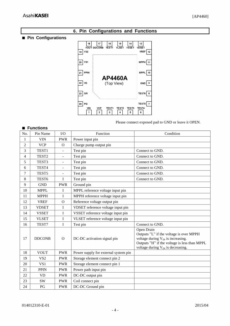
6 . Pin Configurations and Functions
■ Pin Configurations
Please connect exposed pad to GND or leave it OPEN.
■ Functions
No. Pin Name I/O Function Condition
1 VIN PWR Power input pin
2 VCP O Charge pump output pin
3 TEST1 - Test pin Connect to GND.
4 TEST2 - Test pin Connect to GND.
5 TEST3 - Test pin Connect to GND.
6 TEST4 - Test pin Connect to GND.
7 TEST5 - Test pin Connect to GND.
8 TEST6 I Test pin Connect to GND.
9 GND PWR Ground pin
10 MPPL I MPPL reference voltage input pin
11 MPPH I MPPH reference voltage input pin
12 VREF O Reference voltage output pin
13 VDSET I VDSET reference voltage input pin
14 VSSET I VSSET reference voltage input pin
15 VLSET I VLSET reference voltage input pin
16 TEST7 I Test pin Connect to GND.
17 DDCONB O DC-DC activation signal pin
Open Drain
Outputs ”L” if the voltage is over MPPH
voltage during VIN is increasing.
Outputs ”H” if the voltage is less than MPPL
voltage during VIN is decreasing.
18 VOUT PWR Power supply for external system pin
19 VS2 PWR Storage element connect pin 2
20 VS1 PWR Storage element connect pin 1
21 PPIN PWR Power path input pin
22 VD PWR DC-DC output pin
23 SW PWR Coil connect pin
24 PG PWR DC-DC Ground pin
(Top View)
[AP4460]
014012310-E-01 2015/04
- 5 -
7 . Absolute Maximum Ratings
Parameter Symbol min max Unit Condition
Pin Voltage VIN -0.3 6.5 V
Operation Temperature Ta -30 85 ℃
Storage Temperature TSTG -40 150 ℃
Junction Temperature Tj -40 150 ℃
Power Dissipation PD - 2.9 W (Note 2)
Note 1. All voltages are with respect to GND, unless otherwise specified.
Note 2. 2-layer board is used. This is calculated as θJA=42C/W. (Metal area of each layer should be more than
70%, Exposed Pad should be connected to GND)
WARNING: Operation at or beyond these limits may result in permanent damage to the device. Normal
operation is not guaranteed at these extremes.
8 . Recommended Operating Conditions
Parameter Symbol Condition min typ max Unit
Input Voltage (VIN pin) VVIN VVD>VPORL (after start-up) 0.14 - VVDTGT V
MPPH Voltage VMPPH 0.16 - 0.8 V
MPPL Voltage VMPPL VMPPH>VMPPL 0.14 - 0.7 V
Output Voltage VVDTGT 2.5 - 4.0 V
Power supplying threshold VVOUTEN 2.2 - 0.94×VVDTGT V
Stop power supply threshold VVOUTDIS 2.0 - 0.90×VVSSET V
Operation Temperature Ta -30 - 85 ℃
Junction Temperature Tj -30 - 95 ℃
Reference resistor 1 - ROUT+RVDSET+RVSSET+RVLSET 3.6 4 4.4 MΩ
Reference resistor 2 - RIN+RMPPH+RMPPL 4.6 4 4.4 MΩ

[AP4460]
014012310-E-01 2015/04
- 6 -
9 . Electrical Characteristics
(Ta=25℃,The external Circuit is as Figure 13, unless otherwise specified.)
Parameter Symbol Condition min typ max Unit
Start-up Circuit
Minimum input voltage to
start-up operation VINSTUP Tj≧25℃ - 0.35 0.40 V
Stop start-up operation
(When VD is increasing) VPORH 1.8 1.9 2.0 V
Restart start-up operation
(When VD is decreasing) VPORL 1.7 1.8 1.9 V
DC-DC Converter
VVDTGT voltage VVDTGT - 4×VVDSET - V
VVDTGT voltage accuracy - -5 - +5 %
VVDTGT hysteresis VVDTGTHYS 0.01×VVDTGT 0.03×VVDTGT 0.05×VVDTGT V
High-side on resistance RONTOP - 1.5 - Ω
Low-side on resistance RONBOT - 0.6 - Ω
Low-side on Time TON VVD=3.3V 2.3 4.5 6.8 μs
VD pin internal consumption
current IQVD
VVD=3.3V (When DC-DC converter
is in skip state) - 4.5 15 μA
MPPT Circuit
Accuracy of VVIN to activate
DC-DC(Include VOSMPP)
VMPPH 0.55V<set value<0.8V -5 0 +5 %
VMPPH1 0.25V<set value -7 0 +7 %
Accuracy of VVIN to be skip
state(Include VOSMPP)
VMPPL 0.40V<set value<0.7V -5 0 +5 %
VMPPL1 0.25V<set value -7 0 +7 %
Power Path Switch
F1 switch ON resistance RF1 VD>2.5V, 20mA - 2.5 5 Ω
F2 charge switch ON
resistance RF2C VS1>2.5V, 2mA - 200 300 Ω
F2 discharge switch ON
resistance RF2D VS2>2.5V, 20mA - 2 5 Ω
F3 switch ON resistance RF3 VS1>2.5V, 20mA - 2 5 Ω
F1 switch ON voltage VF1ON VD pin - VVDTGTH - V
F1 switch OFF voltage VF1OFF VD pin - VVDTGTH
-VVDTGTHYS - V
F2 charge switch ON voltage
(when charging) VVS2CHG VS1 pin -
4×VVSSET
×1.03 - V
F2 charge switch OFF voltage
(when charging) VVS2HLD VS1 pin -
4×VVSSET
×0.97 - V
F2 discharge switch ON
voltage (when discharging) VVS2DCH VS1 pin -
4×VVSSET
×0.94 - V
F2 discharge switch OFF
voltage (when discharging) VVS2DIS VS1 pin - 4×VVLSET - V
F3 switch ON voltage VVOUTEN VS1 pin - 4×VVSSET -
F3 switch OFF voltage VVOUTDIS VS1 pin - 4×VVLSET
×0.97 - V
F1, F2, F3 Control Voltage
Accuracy - Include VVRFEF accuracy -5 0 +5 %
Reference Voltage
Reference Voltage Output VVREF 1.187 1.236 1.285 V
Current Consumption

[AP4460]
014012310-E-01 2015/04
- 7 -
Parameter Symbol Condition min typ max Unit
VS1, VS2, VOUT pin total
current (Note 3) - VVD<VPORL - 10 20 nA
Protect Function
F2 discharge switch over
current protection IF2CLIM VS1 pin grounding 50 250 700 mA
F3 switch over current
protection IF3CLIM VOUT pin grounding 50 250 700 mA
VD over voltage protection VOV 4.2 4.45 4.7 V
VD over voltage protection
hysteresis VOVHYS 0.35 0.45 0.55 V
Logic I/O
DDCONB Output Voltage VOLDDCON I load<10μA 0 - 0.3 V
DDCONB Leakage Current IOHDDCON VDDCON<4V - 1 10 nA
Note 3. If there is no input power and VVD<VPORL, F1 becomes off and F2 and F3 become on. The internal current
consumption of the IC is 10nA(typ) at this time.

[AP4460]
014012310-E-01 2015/04
- 8 -
10 . Functional Descriptions
10.1 Operation The AP4460 is a synchronous step-up DC-DC converter that can be activated by a single solar cell. The IC
has a power management function which supplies power to an external system, charges super capacitors, or
controls the power path to supply power from the super capacitor to the external system. The AP4460 can be
operated from 0.35V (typ) at the VIN pin. The start-up circuit is operated when VVIN voltage reaches VINSTUP.
Then, the internal charge pump circuit boosts VVIN voltage and charges the capacitor connected to the VCP
pin (CVCP). When the VCP voltage reaches enough level, the internal start-up circuit switches the N-channel
MOSFET transistor (S1) and charges the external capacitor connected to the VD pin (CVD). The start-up
circuit is stopped when the VD voltage reaches VPORH level, then the DC-DC converter starts the operation.
When the VD voltage drops to the level less than VPORL, the DC-DC converter stops and the start-up circuits
is operated again.
Figure 2. State transition of Start-up and DC-DC operation
The DC-DC converter activates the N-channel MOSFET transistor (N1) during TON period to charge the coil.
After TON period, the energy stored in the coil is charged to the CVD capacitor by a power switching of N1
transistor (becomes OFF) and the P1 transistor (becomes ON). The control circuits of the DC-DC sets the P1
transistor off when the SW voltage becomes less than the VD voltage, and then the N1 transistor turns on. The
operation of DC-DC converter is controlled by three reference voltages such as VDSET, MPPL and MPPH
voltages. The VDSET voltage controls the output voltage level (VVDTGT) of DC-DC converter. When the VD
voltage reaches VVDTGT level, the DC-DC converter stops the switching operation and enters 'Skip' state to save
current consumption. When the VD voltage becomes less than VVDTGT - VVDTGTHYS, the DC-DC converter goes to
'Switching' state and boosts the VD voltage. The inputs of the MPPH pin and the MPPL pin (VMPPH and VMPPL)
control the input voltage of the DC-DC converter (VVIN) for effective voltage level of a solar cell. When the VVIN
voltage becomes less than VMPPTL voltage, the DC-DC converter stops switching operation and goes to Skip state
until VVIN voltage reaches VMPPTH voltage. By adjusting input levels of the MPPH pin and the MPPL pin (VMPPH
and VMPPL), the maximum output solar power can be efficiently generated.
The DDCONB (N-channel MOSFET open drain) pin outputs “L” when VVIN voltage is in between VMPPL and
VMPPH. The DC-DC converter has the over voltage protection function for the VD pin. When the VD voltage
exceeds VOV level, the DC-DC converter transitions to Skip state to prevent further voltage increase. When the
VD voltage becomes lower than VOV-VOVHYS, the converter restarts switching operation.
Figure 3. State Transition of DC-DC Operation

[AP4460]
014012310-E-01 2015/04
- 9 -
F1, F2 and F3 switches compose the Power Path function. The F1 switch is placed between the PPIN pin and the
VS1 pin, F2 switch is placed between the VS1 pin and the VS2 pin and F3 switch is placed between the VS1 pin
and the VOUT pin. The F1 switch is synchronized with DC-DC convertor statement that is controlled by the VD
condition. When the VD voltage reaches VVDTGT by DC-DC converter, the F1 switch becomes ON state and the
VD charge is transferred to VS1 to charge the external capacitor until VD voltage becomes less than
VVDTGT-VVDTGTHYS. In other situations, the F1 switch is in OFF state to prevent reverse current flowing from the
VS1 pin to the VD pin. When the VS1 voltage reaches VVOUTEN, the F3 switch becomes ON state and the VOUT
output is available for system loads. The F3 switch is turned OFF when the VS1 voltage becomes less than
VVOUTDIS. When the VS1 voltage reaches VVS2CHG, the F2 switch changes to ON state and the VS1 charge is
transferred to the capacitor connected to the VS2 pin until the VS1 voltage becomes VVS2HLD. When VS1 voltage
drops less than VVS2DCH, the F2 switch also becomes ON state and the VS2 charge is transferred to the capacitor
connected to the VS1 pin. If the VS1 voltage is below VVOUTDIS, the F2 switch is turned OFF. Unnecessary power
dissipation of the external system can be reduced by setting VOUTDIS higher than the lowest operation voltage of
the external system connected to the VOUT pin. When the VD voltage becomes less than VVPORL, the F2 and F3
switches become ON state. At this time, if the capacitor connected to the VS2 pin (CVS2) is charged enough, the
power supply operation to the external system is continued. In case the VD voltage again reaches VVDTGT, the F2
and F3 switches remain in ON state if the VS1 voltage is over VVOUTDIS×1.03. If VS1 voltage is below VVOUTDIS,
the F2 and F3 switches change to OFF state.
Figure 4. State Transition of the Power Path Switches
10.2 Determine the control threshold of the DC-DC converter and power path Four resistors are needed to connect in series between the VREF pin and GND to determine the output target of
the DC-DC convertor (VVDTGT), the output start voltage of the VOUT pin and charge/discharge threshold of the
super capacitor. The voltages between each resistor should be input to the VDSET pin, the VSSET pin and the
VLSET pin. The control threshold of the DC-DC convertor input voltage can be determined by connecting three
resistors in series between the VREF pin and GND, and the voltages between each resistor should be input to the
MPPH pin and the MPPL pin. The connection of resistors is shown in Figure 5.
Figure 5. Resistor connection circuit

[AP4460]
014012310-E-01 2015/04
- 10 -
Determination of the control threshold voltage and external resistors
Table 1. Calculation of the control threshold voltage
Symbol Calculation Formula
VMPPL VREF×RMPPL / (RMPPL+RMPPH+RIN)
VMPPH VREF×(RMPPL+ RMPPH)/ (RMPPL+RMPPH+RIN)
VVDSET VREF×(RVDSET+RVSSET+ RVLSET)/ (ROUT+ RVDSET+RVSSET+ RVLSET)
VVSSET VREF×(RVSSET+ RVLSET)/ (ROUT+ RVDSET+RVSSET+ RVLSET)
VVLSET VREF×(RVLSET)/ (ROUT+ RVDSET+RVSSET+ RVLSET)
Note 4. Refer to 9. Electrical Characteristics as for VVDTGT, F2 charge/discharge switch ON/OFF voltage and F3
switch ON voltage.
Table 2. Example settings of the external resistors, VMPPL and VMPPH (typ)
VREF RMPPL RMPPH RIN VMPPL VMPPH
1.236V 1.6MΩ 0.2MΩ 2.4MΩ 0.471V 0.530V
Note 5. RMPPL+RMPPH+ RIN should be more than 3.6MΩ. Above setting is just an example, please choose
appropriate numbers according to the input conditions.
Table 3. Example settings of VDSET, VSSET and VLSET (typ)
VREF ROUT RVDSET RVSSET RVLSET VVDSET VVSSET VVLSET
1.236V 1.3MΩ 0.24MΩ 0.56MΩ 1.8MΩ 3.296 / 4
=0.824V
2.992 / 4
= 0.748V
2.282 / 4
= 0.571 V
Note 6. ROUT+RVDSET+RVSSET+RVLSET should be more than 3.6MΩ. Above setting is just an example, please
choose appropriate numbers according to the input conditions.
Figure 6. Control Threshold Voltages

[AP4460]
014012310-E-01 2015/04
- 11 -
10.3 Timing Chart
Figure 7. Timing Chart 1: from Start-up to Charge (No Initial Charging)
Figure 8. Timing Chart 2: from Start-up to Charge (With Initial Charging)

[AP4460]
014012310-E-01 2015/04
- 12 -
Figure 9. Timing Chart 3: (Left) VIN decrease, (Right) Load increase
Figure 10. Timing Chart 4: Control VIN voltage

[AP4460]
014012310-E-01 2015/04
- 13 -
10.4 Input/output Current Characteristic
Figure 11. Circuit Example
Internal current consumption of each pin is shown in Figure 12.
Figure 12. The consumption for VD and VS1 pin
・In the case of Start-up:
VD pin current (IVD, inflow into VD pin) is about 2.2uA and VS1 pin current (IVS1, inflow into VS1 pin)
is about 10nA before VVD reaches to VPORH voltage. (In case of VVD < VPORL, F2 switch= ON, the total
internal consumption of VS1 and VS2 pins is 10nA.)
・In the case of DC-DC switching:
After VVD reaches to VPORH, until VVD drops to VPORL, IVD is 5.4uA~1mA depends on switching period
and VVD voltage.
・In the case of DC-DC skip (intermittent action):
After VVD reaches to VTGT, internal current consumption is about 4.7uA. IVS1 consumption is determined
by VS1 pin voltage and internal resistor. (Maximum IVS1 is 500nA when VS1 voltage= 4V) After VVD
reaches to VTGT, until VVD drops to VVDTGT-VVDTGTHYS, switch F1= OFF, the adverse current (from VS1
pin to VD pin) is not occurred. When VVD reaches VPORL, IVD is about 2.2uA and IVS1 is about 10nA.

[AP4460]
014012310-E-01 2015/04
- 14 -
11 . Recommended External Circuit
■ Recommended External Circuit
Figure 13. Recommended External Circuit
■ Recommended External Components
Item Symbol Value Parts No. Note
VIN capacitor CIN 10μF Ceramic (Note 7)
VCP capacitor CVCP 100pF Ceramic
VD capacitor CVD 33μF Ceramic
PPIN resistor RPPIN 330Ω
VS1 capacitor CVS1 470μF
VS2 capacitor CVS2 - (Note 8)
VREF capacitor CVREF 1nF Ceramic
VDSET capacitor CVDSET 100pF Ceramic
MPPH capacitor CMPPH 100pF Ceramic
Output control resistor ROUT 1.3MΩ (Note 9)
VDSET resistor RVDSET 0.24MΩ 3.296V(Note 9)
VSSET resistor RVSSET 0.56MΩ 2.992V(Note 9)
VLSET resistor RVLSET 1.8MΩ 2.282V(Note 9)
Input control resistor RIN 2.4MΩ (Note 9)
MPPH resistor RMPPH 0.2MΩ 0.530V(Note 9)
MPPL resistor RMPPL 1.6MΩ 0.471V(Note 9)
DDCONB resistor RDDCONB 33MΩ 100nA
Coil L 22μH VLF403215MT-220M(TDK) or
VLF302510MT-220M(TDK)
Note 7. The capacitance of the CIN depends on the solar cell. Please choose the suitable value.
Note 8. A super capacitor or a rechargeable battery is usable.
Note 9. Refer to 10.2 for settings of the control threshold voltage and resistors.

[AP4460]
014012310-E-01 2015/04
- 15 -
12 . Package
■ Outline Dimensions (Unit: mm)
■ Recommended Foot Print (Unit : mm)
Expand A part

[AP4460]
014012310-E-01 2015/04
- 16 -
■ Marking
XXXXX
YWWA
(1) 1pin Indication
(2) Market Code:4460A
(3) Year Code (last 1 digit)
(4) Week Code
(5) Management Code
(1)
(2)
(3) (4) (5)

[AP4460]
014012310-E-01 2015/04
- 17 -
11 . Revise History
Date
(YY/MM/DD)
Revision Page Contents
14/12/09 00 - First edition
15/04/16 01 10 Table 2. error correction

[AP4460]
014012310-E-01 2015/04
- 18 -
IMPORTANT NOTICE
0. Asahi Kasei Microdevices Corporation (“AKM”) reserves the right to make changes to the information contained in this document without notice. When you consider any use or application of AKM product stipulated in this document (“Product”), please make inquiries the sales office of AKM or authorized distributors as to current status of the Products.
1. All information included in this document are provided only to illustrate the operation and application examples of AKM Products. AKM neither makes warranties or representations with respect to the accuracy or completeness of the information contained in this document nor grants any license to any intellectual property rights or any other rights of AKM or any third party with respect to the information in this document. You are fully responsible for use of such information contained in this document in your product design or applications. AKM ASSUMES NO LIABILITY FOR ANY LOSSES INCURRED BY YOU OR THIRD PARTIES ARISING FROM THE USE OF SUCH INFORMATION IN YOUR PRODUCT DESIGN OR APPLICATIONS.
2. The Product is neither intended nor warranted for use in equipment or systems that require extraordinarily high levels of quality and/or reliability and/or a malfunction or failure of which may cause loss of human life, bodily injury, serious property damage or serious public impact, including but not limited to, equipment used in nuclear facilities, equipment used in the aerospace industry, medical equipment, equipment used for automobiles, trains, ships and other transportation, traffic signaling equipment, equipment used to control combustions or explosions, safety devices, elevators and escalators, devices related to electric power, and equipment used in finance-related fields. Do not use Product for the above use unless specifically agreed by AKM in writing.
3. Though AKM works continually to improve the Product’s quality and reliability, you are responsible for complying with safety standards and for providing adequate designs and safeguards for your hardware, software and systems which minimize risk and avoid situations in which a malfunction or failure of the Product could cause loss of human life, bodily injury or damage to property, including data loss or corruption.
4. Do not use or otherwise make available the Product or related technology or any information contained in this document for any military purposes, including without limitation, for the design, development, use, stockpiling or manufacturing of nuclear, chemical, or biological weapons or missile technology products (mass destruction weapons). When exporting the Products or related technology or any information contained in this document, you should comply with the applicable export control laws and regulations and follow the procedures required by such laws and regulations. The Products and related technology may not be used for or incorporated into any products or systems whose manufacture, use, or sale is prohibited under any applicable domestic or foreign laws or regulations.
5. Please contact AKM sales representative for details as to environmental matters such as the RoHS compatibility of the Product. Please use the Product in compliance with all applicable laws and regulations that regulate the inclusion or use of controlled substances, including without limitation, the EU RoHS Directive. AKM assumes no liability for damages or losses occurring as a result of noncompliance with applicable laws and regulations.
6. Resale of the Product with provisions different from the statement and/or technical features set forth in this document shall immediately void any warranty granted by AKM for the Product and shall not create or extend in any manner whatsoever, any liability of AKM.
7. This document may not be reproduced or duplicated, in any form, in whole or in part, without prior written consent of AKM.