stick diagram basics
TRANSCRIPT
INTRODUCTION TO STICK DIAGRAMS AND
LAYOUTS
Presented by Sushanth kj Asst.prof. detp. Of ece Bearys institute of
technology mangalore
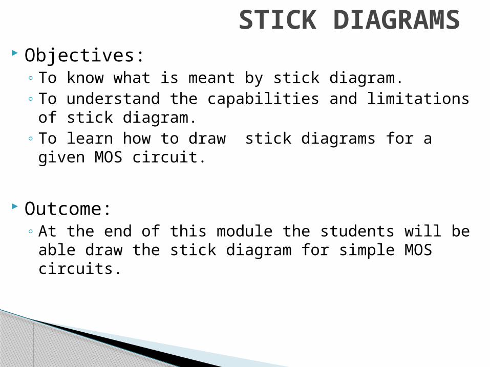
Objectives:◦ To know what is meant by stick diagram.◦ To understand the capabilities and limitations of stick
diagram.◦ To learn how to draw stick diagrams for a given MOS
circuit.
Outcome:◦ At the end of this module the students will be able draw
the stick diagram for simple MOS circuits.
STICK DIAGRAMS
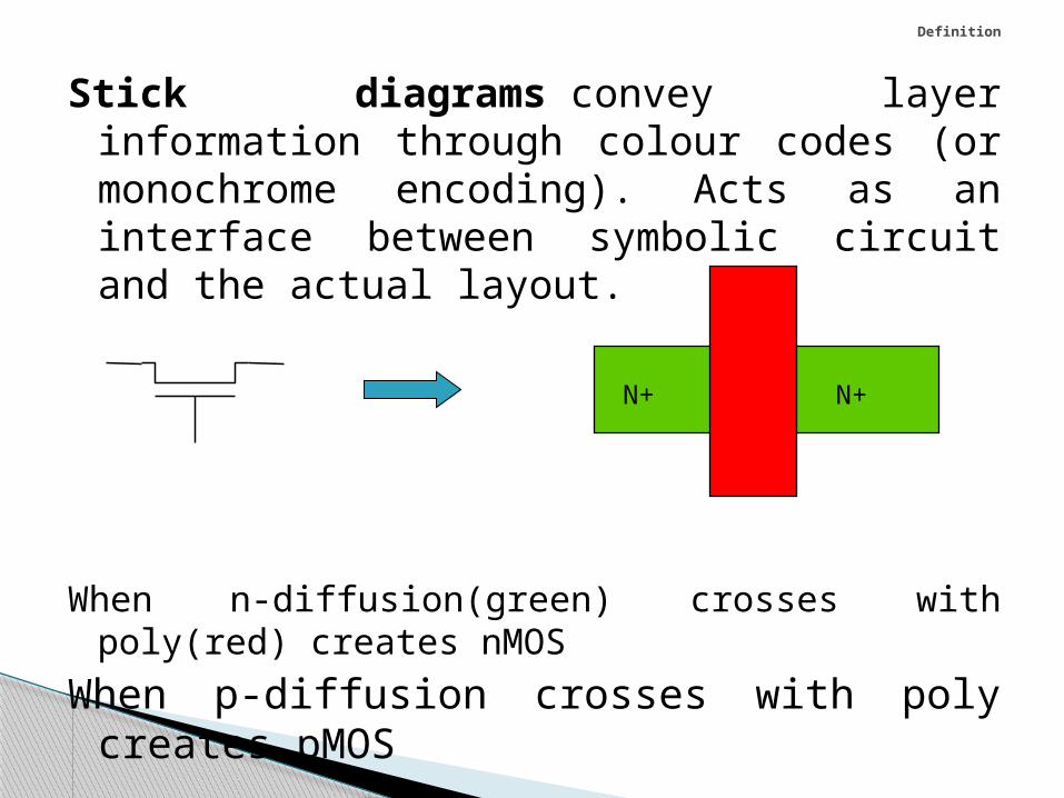
Stick diagrams convey layer information through colour codes (or monochrome encoding). Acts as an interface between symbolic circuit and the actual layout.
When n-diffusion(green) crosses with poly(red) creates nMOS
When p-diffusion crosses with poly creates pMOS
Definition
N+ N+
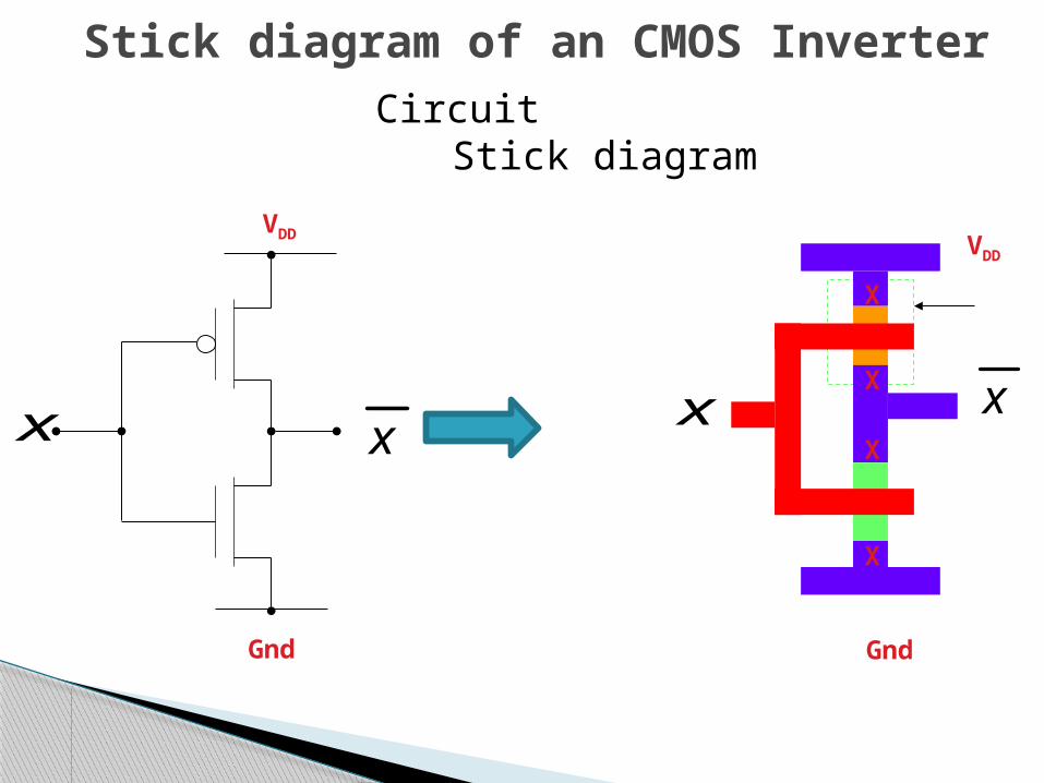
Circuit Stick diagram
Stick diagram of an CMOS Inverter
Gnd
VDD
x x
X
X
X
X
VDD
x x
Gnd
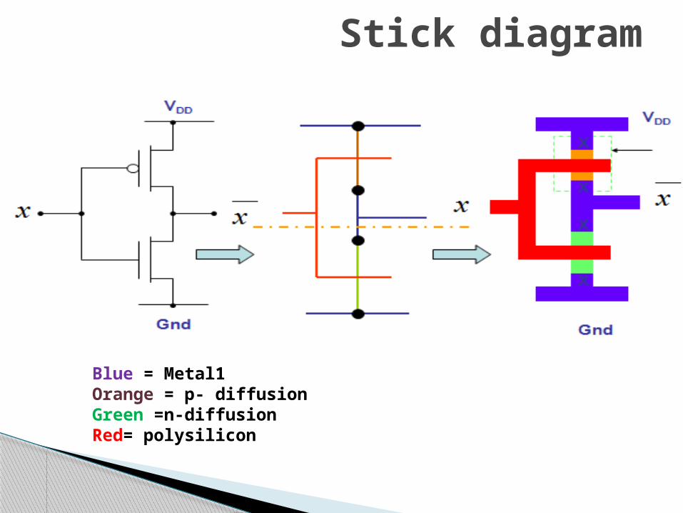
Stick diagram
Blue = Metal1Orange = p- diffusionGreen =n-diffusionRed= polysilicon
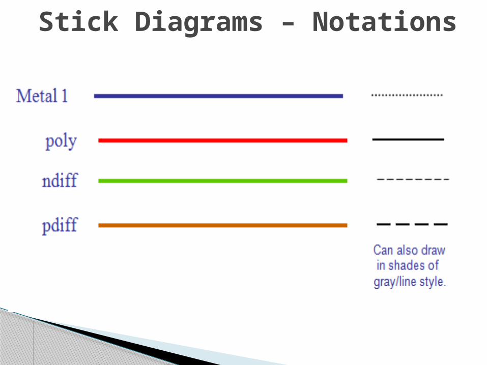
Stick Diagrams – Notations
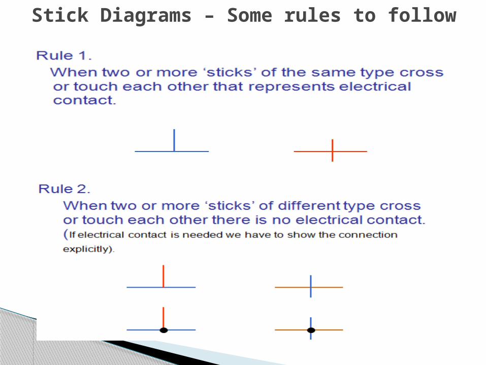
Stick Diagrams – Some rules to follow
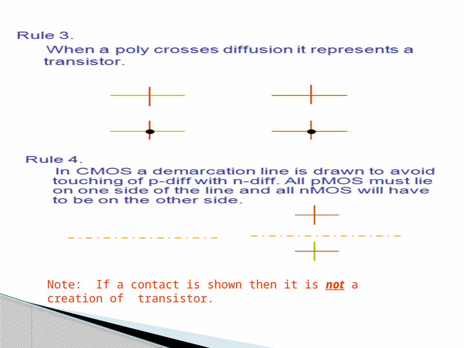
Note: If a contact is shown then it is not a creation of transistor.
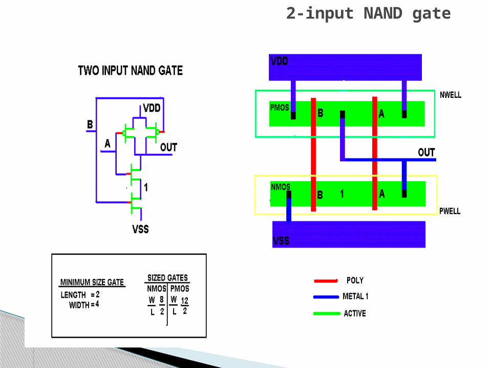
2-input NAND gate
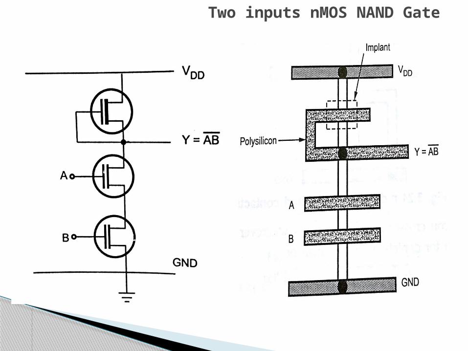
Two inputs nMOS NAND Gate
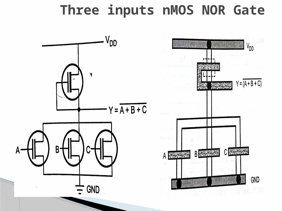
Three inputs nMOS NOR Gate
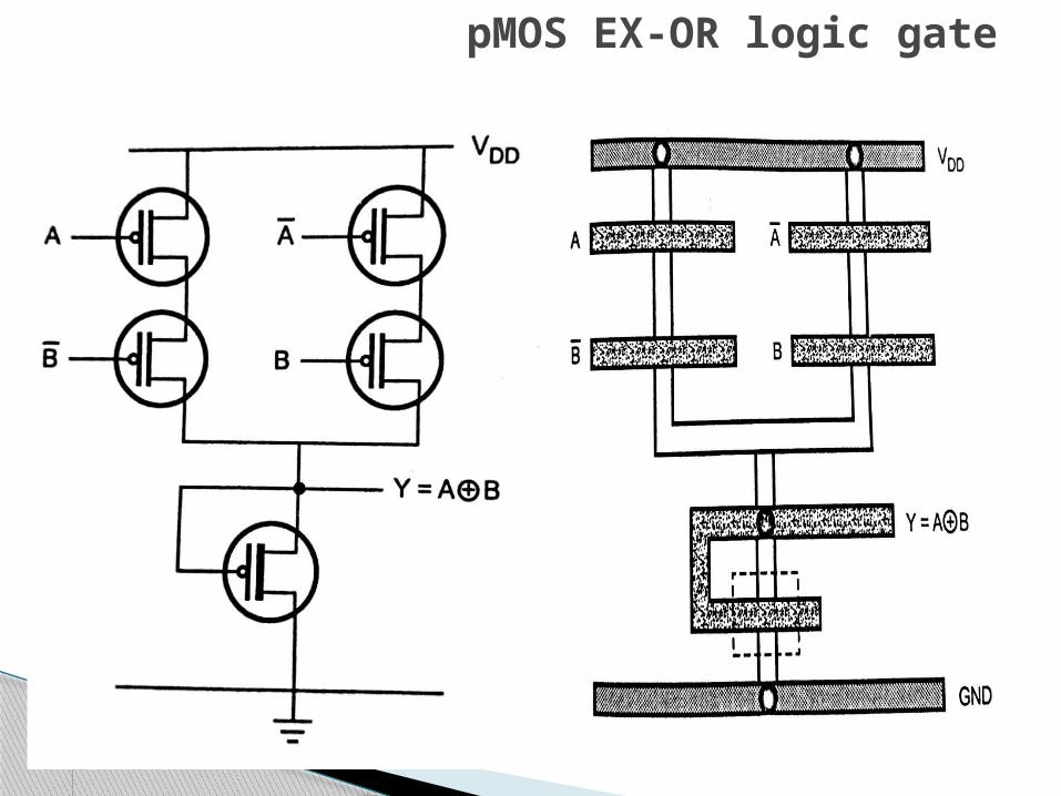
pMOS EX-OR logic gate
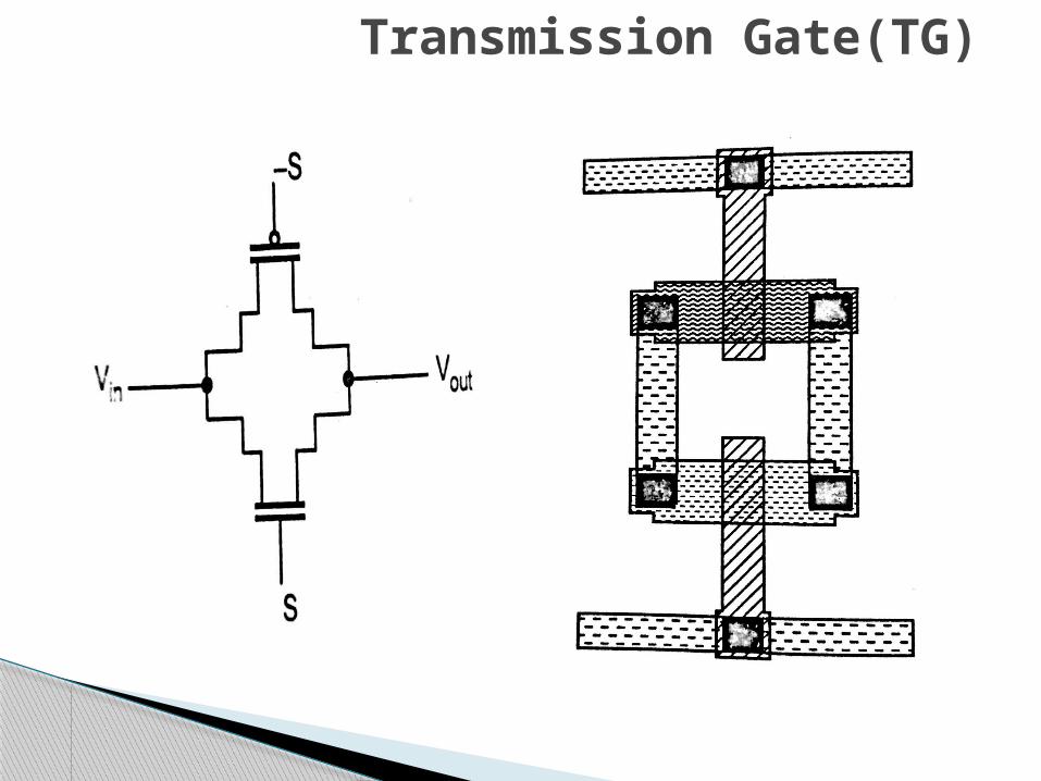
Transmission Gate(TG)
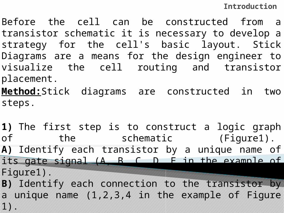
Introduction
Before the cell can be constructed from a transistor schematic it is necessary to develop a strategy for the cell's basic layout. Stick Diagrams are a means for the design engineer to visualize the cell routing and transistor placement.Method:Stick diagrams are constructed in two steps.
1) The first step is to construct a logic graph of the schematic (Figure1). A) Identify each transistor by a unique name of its gate signal (A, B, C, D, E in the example of Figure1). B) Identify each connection to the transistor by a unique name (1,2,3,4 in the example of Figure 1).
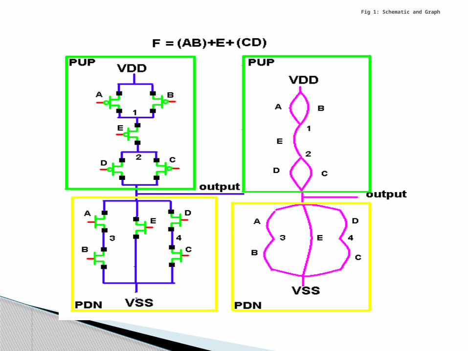
Fig 1: Schematic and Graph
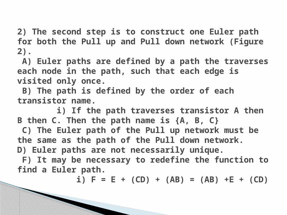
2) The second step is to construct one Euler path for both the Pull up and Pull down network (Figure 2). A) Euler paths are defined by a path the traverses each node in the path, such that each edge is visited only once. B) The path is defined by the order of each transistor name. i) If the path traverses transistor A then B then C. Then the path name is {A, B, C} C) The Euler path of the Pull up network must be the same as the path of the Pull down network. D) Euler paths are not necessarily unique. F) It may be necessary to redefine the function to find a Euler path. i) F = E + (CD) + (AB) = (AB) +E + (CD)
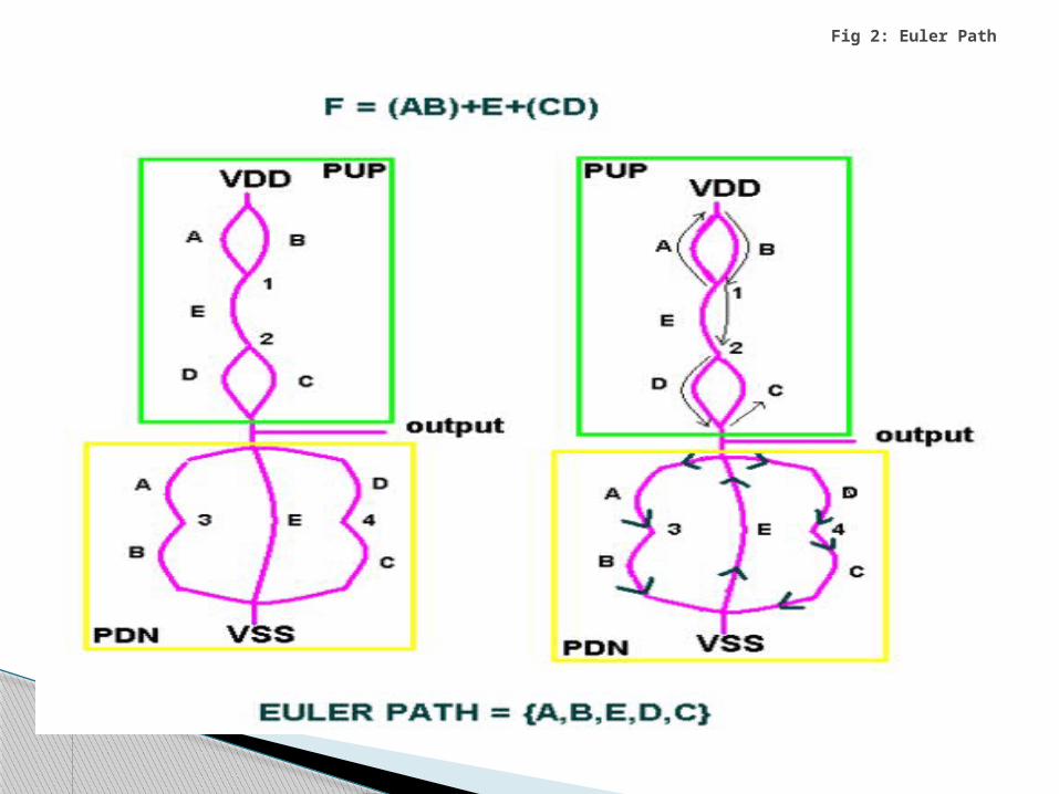
Fig 2: Euler Path
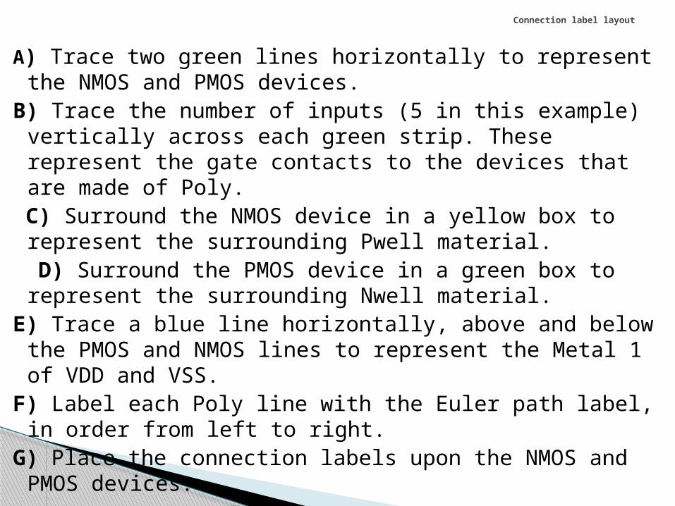
A) Trace two green lines horizontally to represent the NMOS and PMOS devices.
B) Trace the number of inputs (5 in this example) vertically across each green strip. These represent the gate contacts to the devices that are made of Poly.
C) Surround the NMOS device in a yellow box to represent the surrounding Pwell material.
D) Surround the PMOS device in a green box to represent the surrounding Nwell material.
E) Trace a blue line horizontally, above and below the PMOS and NMOS lines to represent the Metal 1 of VDD and VSS.
F) Label each Poly line with the Euler path label, in order from left to right.
G) Place the connection labels upon the NMOS and PMOS devices.
Connection label layout
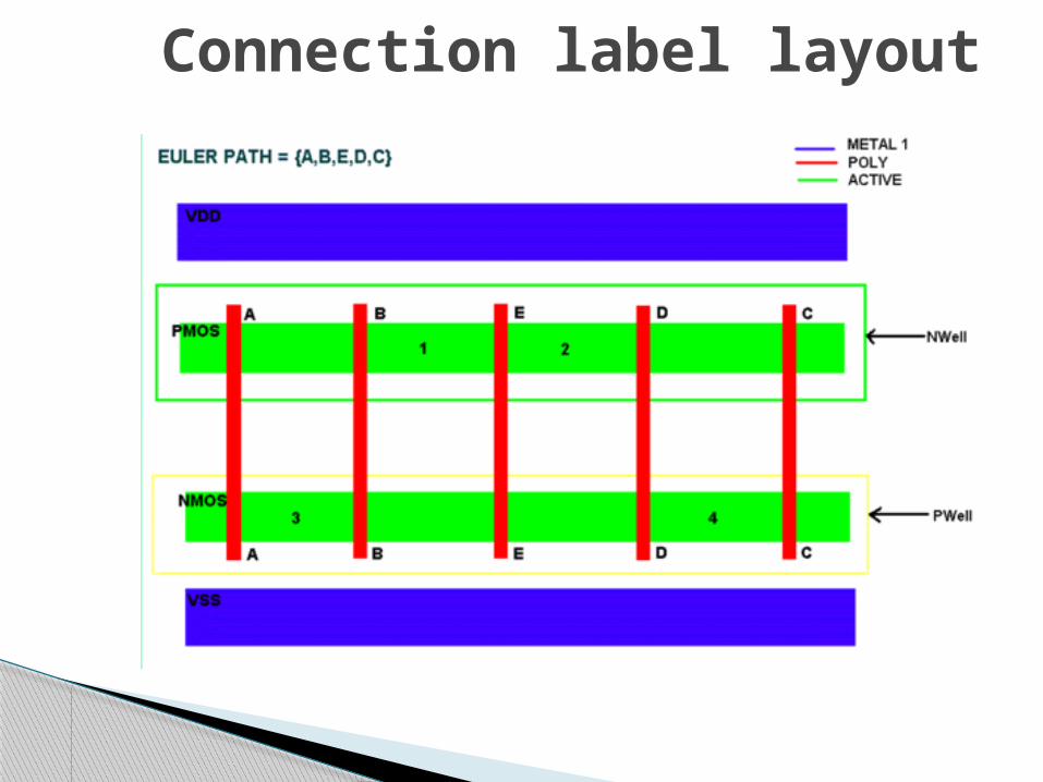
Connection label layout
A) Notice that Poly and Metal 1 can overlap. B) Avoid routing signals that are side by side for
long lengths. This adds capacitance to the device. C) Avoid all interconnect overlap if possible. This
adds capacitance to the device. D) Strive for simplicity. This will later provide the
smallest and fastest devices. E) You can use Poly, Metal 2, and even Active to
interconnect your device. i) Poly and especially Active adds resistance to you
device. ii) Avoid using Metal 2 if possible. Metal 2 is another
layer to your device that you will probably need in the next heiarchy up.
Interconnection of the Device
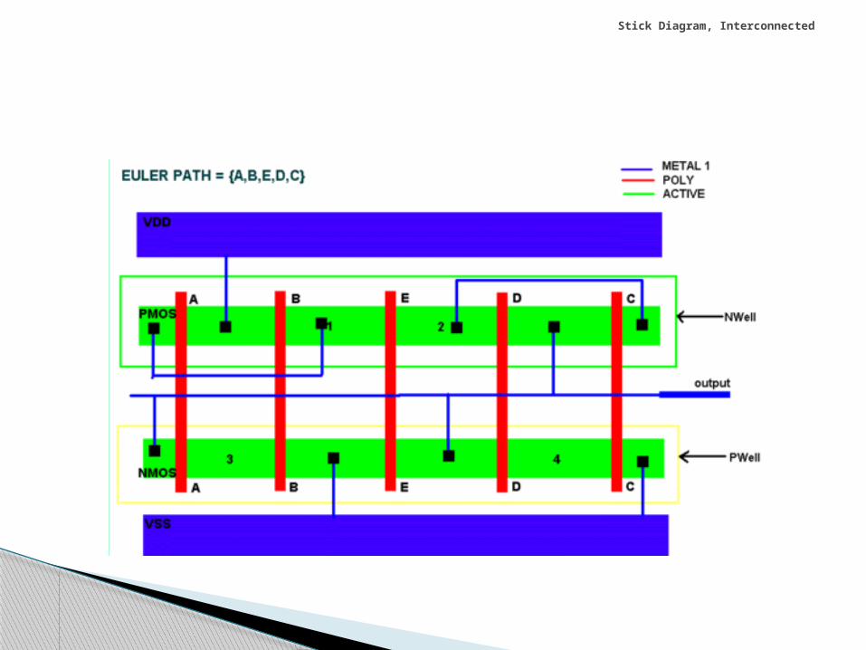
Stick Diagram, Interconnected