students' international research projects technical report 2012
TRANSCRIPT

National Institute of Technology Durgapur, INDIA
Students’ International Research Projects Technical Report 2012-2013
Volume 5

[Blank page]

From Director’s Desk
I am pleased to note that, like the last four years, we are publishing the “Students’ International Research Projects; Technical Report 2012-2013; Volume 5” this year too. This report presents an overview of the research activities of our students during internship and presentation in international conferences abroad. Over the last few years, National Institute of Technology Durgapur has been trying to initiate the students to active research early. They are supervised by the faculty members of the Institute and are financially supported by the Institute for their research visits to conferences in India and abroad and for research internship abroad. This has exposed them to the research activities being carried out in the premier universities in the world and encouraged them to interact directly with the most eminent researchers around the globe. I wish the authors will pursue research and innovation in their professional life. Professor T. Kumar Director National Institute of Technology Durgapur

[blank page]

AUTHORS
Avishek Dey
Abhisek Mukhopadhyay Anurag Bhattacharyya
Arkaprava Chaudhuri
Debjani Chakraborty Kumar Gaurav Singh
Manisha De
Ria Mishra
Shivani Bansal
Soumya Sarkar
Souransu Nandi
Sudipto Majumder
AUTHORS
Vivek Kumar Singh
Anish Singhania
Ankit Bhardwaj
Arup Kanti Kole
Bikash Choudhury
Debanjana Baksi
Divyam Saran
Arambam James Singh Pritha Das Saupayan Mazumdar

Contents Title Author Page
No. RESEARCH INTERNSHIP:
A COMPARATIVE STUDY OF MANGANESE OXIDE/GRAPHENE COMPOSITES AS SUPERCAPACITOR ELECTRODES
Avishek Dey
1
INVESTIGATING THE FEASIBILITY OF A TRAVELLING-WAVE CHOPPER FOR THE CLEAN SEPARATION OF 10 MHZ BUNCHES AT HIE-ISOLDE
Abhisek Mukhopadhyay
3
DESIGN MODIFICATION AND ANALYSIS OF SAA3 STRUCTURE
Anurag Bhattacharyya
5
AN ALLOHEXAPLOID BRASSICA POPULATION DERIVED FROM CROSSES BETWEEN ALLOTETRAPLOID SPECIES SHOWS A RANGE OF FERTILITY AND REGULAR SEGREGATION OF ALLELES
Arkaprava Chaudhuri
7
ELECTROCHEMICAL IMPEDANCE MODELLING OF SODIUM ION BATTERIES
Debjani Chakraborty
9
EFFECTS OF RADIATION AND RADIATION CALCULATION AT CMS CAVERN
Kumar Gaurav Singh
11
DEVELOPMENT OF A TOOL TO CONTROL POWER DISTRIBUTION UNIT (PDU) FOR DETECTOR CONTROL SYSTEMS
Manisha De
13
EFFECTS OF ARSENIC EXPOSURE ON REGULATION OF ANGIOGENESIS BY VEGF-A AND VEGFR-2 IN ZEBRAFISH
Ria Mishra
15
PERFORMANCE ANALYSIS OF HMPID (HIGH MOMENTUM PARTICLE IDENTIFIER DETECTOR) OF ALICE (A LARGE ION COLLIDER EXPERIMENT)
Shivani Bansal
17
RESISTIVE SWITCHING OF TRANSPARENT COMPLEX OXIDE RERAM FILMS
Soumya Sarkar
19
DESIGN AND DEVELOPMENT OF PRINTED CIRCUIT BOARDS FOR DIFFERENT CONTROLLERS OF A POWERED ORTHOSIS
Souransu Nandi
21
MODELLING OF THE ELECTRICAL EQUIVALENT OF RESISTIVE PLATE CHAMBERS
Sudipto Majumder
23
A MULTI-AGENT TEST BED FOR MICROGRID CONTROL
Vivek Kumar Singh
25

CONFERENCES: SEMANTIC WEB-BASED E-COUNSELING SYSTEM
Anish Singhania
27
MODELLING OF MULTIAGENT BASED RAILWAY SYSTEM USING BDI LOGIC
Ankit Bhardwaj
29
EFFECT OF ANNEALING ON YELLOW ORANGE PHOTOLUMINESCENCE EMISSION OF UNCAPPED Mn2+ DOPED ZnS QUANTUM DOTS SYNTHESIZED BY SIMPLE CHEMICAL METHOD
Arup Kanti Kole
31
A FAMILY OF FLEXIBLE OFFSET-TIME BASED WAVELENGTH SCHEDULERS FOR OBS EDGE-NODES
Bikash Choudhury
33
CHAOTIC BLOCK ENCRYPTION WITH POSITION PERMUTATION
Debanjana Baksi
35
QCA MULTIPLEXER BASED DESIGN OF REVERSIBLE ALU
Divyam Saran
37
AGENT BASED TASK SPECIfiC TEAM FORMATION FOR EFFECTIVE DISTRIBUTED DECISION MAKING
Arambam James Singh
39
SUPPLIER SELECTION IN RISK ENVIRONMENT: FUZZY INTERVAL TYPE-2 TOPSIS METHOD
Pritha Das
41
2-Π CROSSTALK NOISE MODEL FOR DEEP SUBMICRON VLSI GLOBAL RC INTERCONNECTS
Saupayan Mazumdar
43

1
A COMPARATIVE STUDY OF MANGANESE OXIDE/GRAPHENE COMPOSITES AS SUPERCAPACITOR ELECTRODES
Avishek Dey
M. Tech student, Department of Physics National Institute of Technology Durgapur, INDIA
Email id: [email protected]
Department of Engineering and Innovation The Open University, Walton Hall, Milton Keynes, MK7 6AA , UK
March 18 – May 10, 2013
Abstract Composites of reduced graphene oxide /Manganese oxide at three different oxidation states of Manganese were successfully synthesized through facile solution based chemical methods. The morphology and microstructure of the as synthesized composites were characterized by Field emission scanning electron microscopy, Raman spectroscopy, X-ray photo electron spectroscopy and High resolution transmission electron microscopy. Introduction Carbon-based materials have been researched extensively as electrodes in electrical energy storage devices such as supercapacitors and batteries, owing to a unique combination of properties such as high surface area, lightweight, good electrical conductivity, compatibility with other materials, and controlled pore size distribution [1-3]. The advent of new forms of carbon materials such as high quality graphene sheets (single layer to a few layers) with superior electrical properties have allowed for the development of new engineered carbons for energy storage [4,5]. Owing to their large in-plane conductivities graphene films are expected to play a crucial role in the development of electrodes for a variety of energy applications such as photo-voltaics [6] and supercapacitors [7]. These materials have recently been used in super capacitor devices to replace conventional carbon electrodes and have shown very good performance [8]. On the other hand transition metal oxides, in particular, manganese oxides are well known for
their use in supercapacitor [9]. In view of the above the present work focuses on the synthesis and characterization of grapheme and Manganese Oxide for applications in energy storage. Experimental Graphene oxide was synthesized using Hummers method [10]. MnO2/GO composite was synthesized by refluxing Graphene oxide and KMnO4 at 160ºC in presence of citric acid. Mn2O3/GO composite was synthesized by ultrasonicating Graphene oxide and KMnO4 in presence of ethylene glycol and then reducing with hydrazine.Mn3O4/GO composite was synthesized by hydrothermal reaction of Graphene oxide and Mn(AC)2 at 200 ºC. Results and Discussion The morphologies of the resulting products were characterized using a scanning electron microscopy (SEM, ZEISS SUPRA 55VP FEGSEM, 20 keV) attached with an energy-dispersive X-ray analysis (EDAX) and transmission electron microscopy (HRTEM; JEM JEOL-2100, 200 keV) The elemental composition was characterized by X-ray photoelectron spectroscopy (Al Kα radiation at 12 kV and 12 mA). Fig (a), (b), (c) shows the SEM images of the composites. From images it can be depicted that the multiple layers of graphene are stacked in the form of flakes. Fig (b) shows the cluster formation of the MnO2 particles on the graphene sheets. Fig (c) shows less agglomeration on the Mn2O3 particles on the graphene sheet. This may be due to the proper
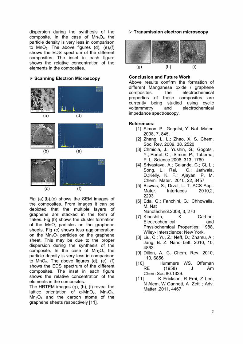
dispersion during the synthesis of the composite. In the case of Mn3O4 the particle density is very less in comparison to MnO2. The above figures (d), (e),(f) shows the EDS spectrum of the different composites. The inset in each figure shows the relative concentration of the elements in the composites.
Scanning Electron Microscopy
(a) (d)
(b) (e)
(c) (f) Fig (a),(b),(c) shows the SEM images of the composites. From images it can be depicted that the multiple layers of graphene are stacked in the form of flakes. Fig (b) shows the cluster formation of the MnO2 particles on the graphene sheets. Fig (c) shows less agglomeration on the Mn2O3 particles on the graphene sheet. This may be due to the proper dispersion during the synthesis of the composite. In the case of Mn3O4 the particle density is very less in comparison to MnO2. The above figures (d), (e), (f) shows the EDS spectrum of the different composites. The inset in each figure shows the relative concentration of the elements in the composites. The HRTEM images (g), (h), (i) reveal the lattice orientation of α-MnO2, Mn2O3, Mn3O4 and the carbon atoms of the graphene sheets respectively [11].
Transmission electron microscopy
(g) (h) (i) Conclusion and Future Work Above results confirm the formation of different Manganese oxide / graphene composites. The electrochemical properties of these composites are currently being studied using cyclic voltammetry and electrochemical impedance spectroscopy. References:
[1] Simon, P.; Gogotsi, Y. Nat. Mater. 2008, 7, 845.
[2] Zhang, L. L.; Zhao, X. S. Chem. Soc. Rev. 2009, 38, 2520
[3] Chmiola, J.; Yushin, G.; Gogotsi, Y.; Portet, C.; Simon, P.; Taberna, P. L. Science 2006, 313, 1760
[4] Srivastava, A.; Galande, C.; Ci, L.; Song, L.; Rai, C.; Jariwala, D.;Kelly, K. F.; Ajayan, P. M. Chem. Mater. 2010, 22, 3457
[5] Biswas, S.; Drzal, L. T. ACS Appl. Mater. Interfaces 2010,2, 2293
[6] Eda, G.; Fanchini, G.; Chhowalla, M. Nat Nanotechnol.2008, 3, 270
[7] Kinoshita, K. Carbon: Electrochemical and Physiochemical Properties; 1988, Wiley- Interscience: New York.
[8] Liu, C.; Yu, Z.; Neff, D.; Zhamu, A.; Jang, B. Z. Nano Lett. 2010, 10, 4863
[9] Dillon, A. C. Chem. Rev. 2010, 110, 6856
[10] Hummers WS, Offeman RE (1958) J Am Chem Soc 80:1339.
[11] K Erickson, R Erni, Z Lee, N Alem, W Gannett, A Zettl ; Adv. Matter ,2011, 4467
2

3
INVESTIGATING THE FEASIBILITY OF A TRAVELLING-WAVE CHOPPER FOR THE CLEAN SEPARATION OF 10 MHZ BUNCHES
AT HIE-ISOLDE
Abhisek Mukhopadhyay Fourth year B. Tech. student, Department of Electronics & Communication Engg
National Institute of Technology Durgapur, INDIA Email id: [email protected]
CERN, Geneva
May 11 – July 10, 2013
Abstract The feasibility of a travelling wave type chopper at HIE-ISOLDE was investigated using a simple model comprising a chain of synchronised capacitors pulsed at high-voltage. Even with a relatively large transverse aperture of 30mm, it appears feasible to remove the satellite bunches spaced at 75mm without significantly perturbing the main bunch. We estimate that for a chopping voltage of 1.2 kV a string of 20 capacitors is required to impart the required deflection of 4 mrad to beams with A:q = 4:5 and the mechanical length of the system can be kept under 0.5 m. The deflection imparted on the main pulse is . 1% of that received by the discarded satellite bunches and the transverse emittance growth of the beam is small if the rise/fall times are kept below 5 ns. Introduction In order to provide the requested 10MHz beam frequency at HIE-ISOLDE it is proposed to pre-bunch into the 101.28MHz REX-ISOLDE RFQ using an external multi-harmonic buncher (MHB) operatingat a sub-harmonic ten times lower in frequency. As a consequence of the imperfect bunching efficiency of the MHB-RFQ system (80%) some of the ‘out-of-phase’ particles entering the RFQ will be bunched into adjacent buckets outside of the main buckets spaced at a frequency of 10.128 MHz. A chopper structure is required to attain a clean separation of the
10MHz bunches by removing the satellite bunches from the bunch train. Theory / Model The system initially considered consists of a single parallel plate capacitor. in a direction transverse to the beam axis; we neglect the other smaller field components. This field deflects the unwanted satellite bunches onto a slit placed a distance downstream of the chopper, while the nominal bunches (the main bunches that are not kicked) are transmitted through the slit. Then we scale the system up to the level of a higher number of capacitors and introduce structures that make this feasible. The feasibility is achieved by introducing ground planes for effective shielding between two capacitor plates. This is necessary as in their absence the capacitor plates might influence each other leading to undesirable transient performance. In this study we do not focus on the transient performance and assume steady state behaviour. This is primarily a first order study in which we later take into account the complicated scenarios and try solving more problems. But we are convinced that first order study is important to understand the system.

4
Experimental We simulated a simple parallel-plate capacitor using CST EM Studio 2012 assuming that the quasi static approximation is valid for the low frequencies. Fourier decompositions of trapezoidal pulse signals indicate that the most dominant frequency components are below 100 MHz, where the wavelength is 3m. The wavelengths of the time-dependent components of the electric field are therefore much larger than the scale of their spatial variation and to a good approximation the Helmholtz equation can be reduced to the static Laplace equation. We do the required calculations on the basis of a single capacitor, then we scale the structure up to meet the specification. Results and Discussion We arrive at some basic design guidelines for the simplified chopper consisting of an array of independently powered parallel-plate capacitors in the table. The table clearly shows that we can attain the given specifications and have a structure well within the desired range of 0.5m. Length of the plates (l) [mm] 12 Aperture (separation of the plates),d [mm]
30
Distance to ground planes d2 [mm]
2
Separation of shielding planes [mm]
5
Excitation voltage [kV] 1.2 No. of capacitors, N 20 Length of chopper, L_Struct [m] <0.5 ratio <1%
Rise, fall time (tau)[ns] <5 Sleep-time (T) [ns] 5 to 10
Conclusion The feasibility of cleanly separating the main 10.128MHz bunches from the 101.28MHz satellite bunches with a travelling-wave type chopper at HIE-ISOLDE was demonstrated using a model comprising a chain of synchronised capacitors pulsed at high-voltage and by employing the quasi-static approximation for the rf fields. Even with a relatively large transverse aperture of 30mm it is possible to remove the satellite bunches that are separated by d = 75mm without significantly perturbing the main pulse. We estimate that for a chopping voltage of 1.2 kV a string of 20 capacitors is required to impart a deflection of 4 mrad to beams with A:q = 4:5 and the mechanical length of the system can be kept under 0.5 m. The deflection of the main pulse is .1% of that received by the discarded satellite bunches and the transverse emittance growth of the beam is small if the rise/fall times are kept below 5 ns (the sleep-time of the plates should be 5 ns).

DESIGN MODIFICATION AND ANALYSIS OF SAA3 STRUCTURE
Anurag Bhattacharyya B. Tech. third year B. Tech. student, Department of Mechanical Engineering
National Institute of Technology, Durgapur, India
ALICE PH/DT European Organization for Nuclear Research (CERN), Geneva, Switzerland
May - July, 2013
Abstract
The proposed extension is shown below: The following report describes the tasks performed during the summer internship at CERN, Geneva, which are listed below:
5
1) Modification of the SAA3 extension using CATIA V5
2) Analysis of the SAA3 beams, using ANSYS WORKBENCH 14.5 and determine the safety of the beams under the proposed loading using different modelling approaches.
3) Analysis of the SAA3 support structure using ANSYS WORKBENCH 14.5 and determine the safety of the structure under the intended loading condition using different modelling approaches.
The final SAA3 structure should be as below: 4) Determine the feasibility and the
safety of the SAA3 wall connection by doing analysis of the connecting bolts
Introduction The main beam pipe in ALICE detector is surrounded by a wall of steel blocks for filtering the beam background detected by ALICE. These steel blocks along with the anti-seismic frame and the support structure together make the SAA3.
. Here the mass of the blocks along with the anti-seismic frame is approximately 52 tonnes.It has been proposed to extend the SAA3 structure for further beam filtering and increased data accuracy by adding another set of blocks and beams to the existing structure. The newer blocks are dimensioned as l=800mm, b=400mm and h= 400mm. total mass of the proposed structure is 35tonnes.
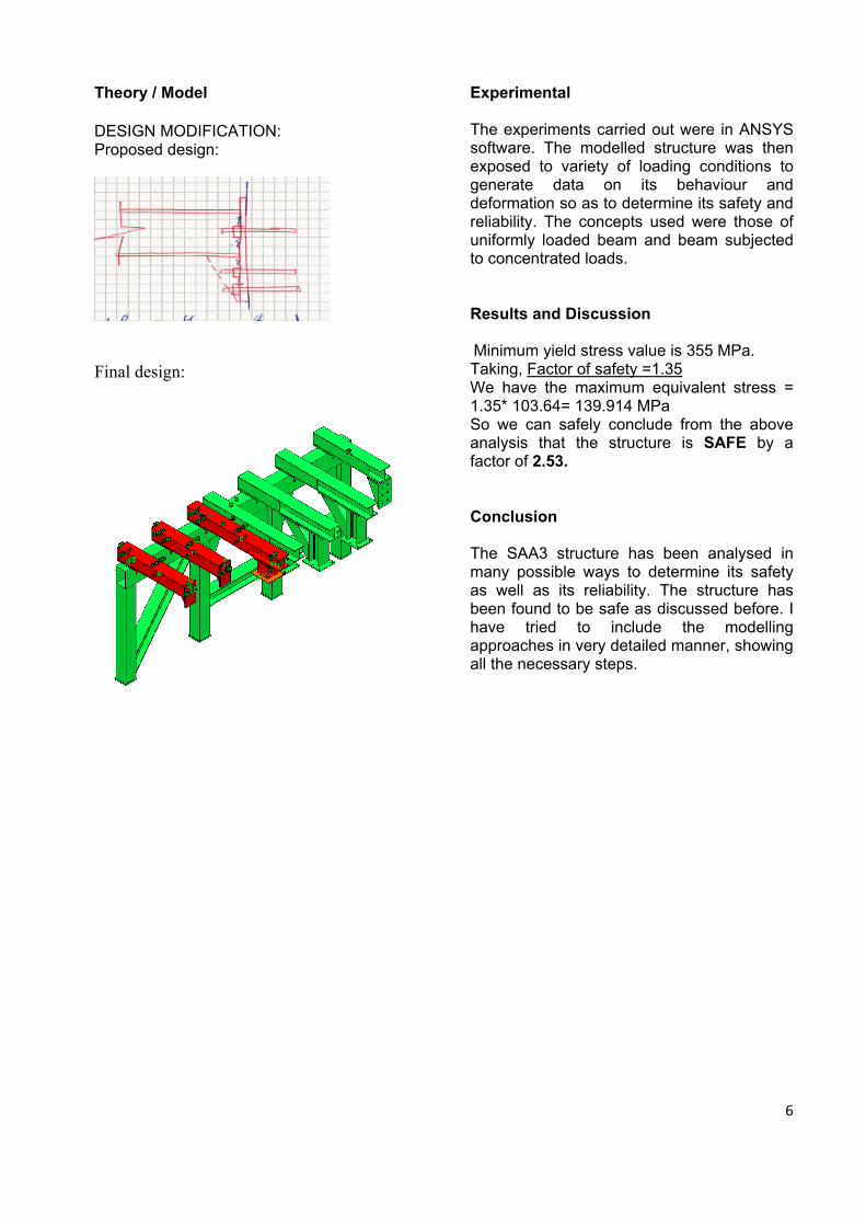
Theory / Model DESIGN MODIFICATION: Proposed design:
Final design:
Experimental The experiments carried out were in ANSYS software. The modelled structure was then exposed to variety of loading conditions to generate data on its behaviour and deformation so as to determine its safety and reliability. The concepts used were those of uniformly loaded beam and beam subjected to concentrated loads. Results and Discussion Minimum yield stress value is 355 MPa. Taking, Factor of safety =1.35 We have the maximum equivalent stress = 1.35* 103.64= 139.914 MPa So we can safely conclude from the above analysis that the structure is SAFE by a factor of 2.53. Conclusion The SAA3 structure has been analysed in many possible ways to determine its safety as well as its reliability. The structure has been found to be safe as discussed before. I have tried to include the modelling approaches in very detailed manner, showing all the necessary steps.
6

7
AN ALLOHEXAPLOID BRASSICA POPULATION DERIVED FROM CROSSES BETWEEN ALLOTETRAPLOID SPECIES SHOWS A RANGE
OF FERTILITY AND REGULAR SEGREGATION OF ALLELES
Arkaprava Chaudhuri Fourth year B. Tech. student, Department of Biotechnology
National Institute of Technology Durgapur, INDIA Email id: [email protected]
School of Agriculture and Food Science, ARC CILR The University of Queensland, Brisbane, Australia
December 10, 2012 – February 15, 2013 Abstract There is a useful allelic contribution from all three of the Brassica genomes present in the cultivated diploid (2n=AA,2n=BB, 2n=CC) and allotetraploid (2n=AABB, 2n=AACC, 2n=BBCC) crop species (canola, cabbage, mustard) in the production of allohexaploid Brassica (2n=AABBCC) which is added with its potential for hybrid heterosis. Characterisation of a population of putative allohexaploids derived from a hybrid parent from the novel cross (B.napus X B.carinata) X B.juncea was done by using techniques like single nucleotide polymorphism (SNP) ,molecular marker assay, flow cytometry and Fluorescent in-situ hybridisation (FISH). Introduction The Brassica genus contains more number of cultivated crop species of any plant genus. Six major crop species are B. rapa (Chinese cabbage, turnip), B. oleracea (cabbage, cauliflower, broccoli), B. nigra (black mustard), B. napus (canola, rapeseed), B. juncea (Indian mustard, leaf mustard) and B. carinata (Ethiopian mustard). Among these species there is an unique correlation: the progenitor diploid species B. rapa (2n = AA), B. oleracea (2n = CC) and B. nigra (2n = BB) gave rise to allotetraploid species B. juncea (2n = AABB), B. napus (2n = AACC) and B. carinata (2n = BBCC) through pairwise crosses .However the strange fact is the absence of natural occurrence of any allohexaploid species (2n=AABBCC), although each pair of genome coexists in the allotetraploid(2n=AABB,AACC,BBCC). Hybridization and polyploidy are potent force
s that allow evolutionary development of new species against their parent species. Hence it is rightfully evident that generation of artificial allohexaploid of Brassica can lead to development of modern crop species which can tolerate a wide range of climatic conditions and also demonstrate outbreeding enhancement of functions over the already available Brassica crops. Experimental
1. Pollen Viabilities: Dissected anthers obtained from flowers (all viable samples were used) were placed on slides, added with 1% acetic-acid carmine solution. The solution basically apart from acting as a dye also prevents pollens from getting disoriented. A cover slip was then placed over the petals of flowers and slowly placed to allow release of pollen grains, which was then viewed under Bright field microscope( 150X –Nikon E400). Oval shaped, stained pollens were considered as viable and shrivelled non-stained ones non-viable. A minimum of around 300 viable pollens were counted from two different flowers obtained from each viable samples.
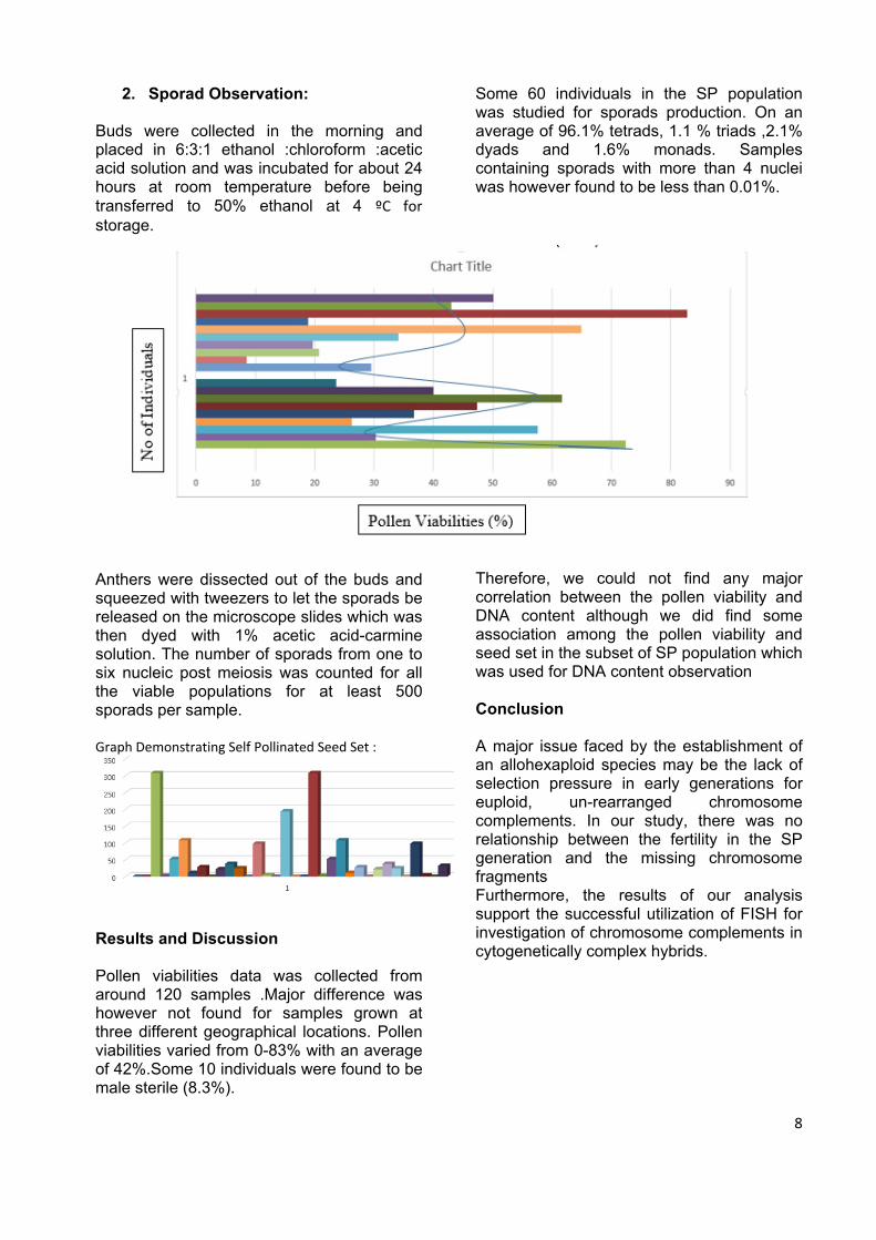
2. Sporad Observation: Buds were collected in the morning and placed in 6:3:1 ethanol :chloroform :acetic acid solution and was incubated for about 24 hours at room temperature before being transferred to 50% ethanol at 4 ºC for storage.
8
Anthers were dissected out of the buds and squeezed with tweezers to let the sporads be released on the microscope slides which was then dyed with 1% acetic acid-carmine solution. The number of sporads from one to six nucleic post meiosis was counted for all the viable populations for at least 500 sporads per sample. Graph Demonstrating Self Pollinated Seed Set :
Results and Discussion Pollen viabilities data was collected from around 120 samples .Major difference was however not found for samples grown at three different geographical locations. Pollen viabilities varied from 0-83% with an average of 42%.Some 10 individuals were found to be male sterile (8.3%).
Some 60 individuals in the SP population was studied for sporads production. On an average of 96.1% tetrads, 1.1 % triads ,2.1% dyads and 1.6% monads. Samples containing sporads with more than 4 nuclei was however found to be less than 0.01%. Therefore, we could not find any major correlation between the pollen viability and DNA content although we did find some association among the pollen viability and seed set in the subset of SP population which was used for DNA content observation Conclusion A major issue faced by the establishment of an allohexaploid species may be the lack of selection pressure in early generations for euploid, un-rearranged chromosome complements. In our study, there was no relationship between the fertility in the SP generation and the missing chromosome fragments Furthermore, the results of our analysis support the successful utilization of FISH for investigation of chromosome complements in cytogenetically complex hybrids.
ELECTROCHEMICAL IMPEDANCE MODELLING OF SODIUM ION BATTERIES
Debjani Chakraborty
Fourth year B. Tech. student, Department of Electrical Engineering, National Institute of Technology Durgapur, India
TUM CREATE, RP1 (Battery group), Singapore May 14- July 12, 2013
Abstract: Energy storage in utility power grids has been known for many years. It is receiving more attention recently due to the proliferation of intermittent renewable energy resources. The basic requirement for large scale storage system is ultra long life cycle, high power capability and low cost. Sodium ion battery (NIB) is a promising alternative to the aforementioned technology. Various tests like cyclic voltammetry, electrochemical impedance spectroscopy (EIS), raman spectroscopy, etc are performed for battery’s performance data analysis. In the project, a technique is developed to study the electrical circuit (model) associated with the chemical environment with the help of the EIS data. Introduction: The entrance of LIBs into the high energy fields, such as electric vehicles and grid storage puts into question the availability of readily accessible lithium in the environment. Sodium ion battery (NIB) is a promising alternative to the aforementioned technology. Sodium metal’s alkaline chemistry is quite similar to that of lithium, just that the size of sodium ion is bigger that lithium ion which sometimes affects the storage and cyclic ability of NIBs. Currently there are many groups of Battery researchers around the globe who are working on high performance, durable electrode material based on the porous 3D NASICON framework, Na 3 V 2 (PO 4 ) 3 /C. After the assembly of the coin cell with the electrodes and electrolyte, the cell is made to undergo tests conducted by a computer controlled ARBIN battery tester. Electrochemical Impedance Spectroscopy is
a test conducted by ARBIN, in which a purely sinusoidal voltage is applied across the cell to study the variation of impedance in frequency domain. From these results and studies the analogy of an electric circuit to a chemical system is presented with the use of Laplace transform to construct the transfer function of the system by studying the nyquist and the bode plots obtained from system data. Thus the electric circuit of the impedance model of such a system is constructed with the help of MATLAB program as a tool. The developed electrochemical impedance model is at a rudimentary stage. It is viable only for studying sodium vanadium phosphate batteries. To make it applicable to other electrode materials, further studies have to be performed to study the interrelation of different parameters of the model. Researchers are developing such models for fuel cells as well.
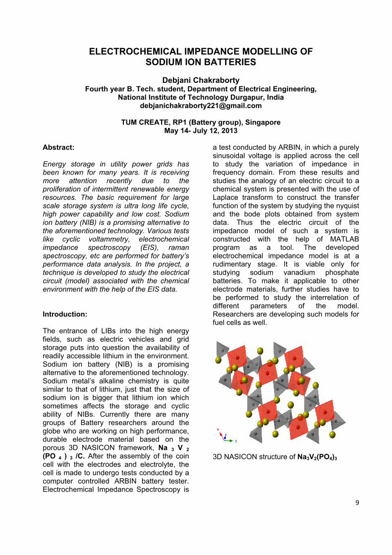
3D NASICON structure of Na3V2(PO4)3
9

Theory: A purely sinusoidal voltage is applied across the cell. E = Em sin (ωt) I = Im sin (ωt-Ψ) Z = E/I Z = Zm (cos (Ψ)+j sin (Ψ)) = real(Z)+ j.img(Z) Experimental:
This is the electrical circuit representing the model. Here Q means the double layer capacitance (Cdl) which is not an ideal capacitance. Here Q is a constant phase element. For which the impedance Z = 1/Q(jω)n. For ideal capacitance n tends to 1. Rs refers to the solution resistance which comes into the picture due to movement of sodium ions in the electrolyte. Rct refers to charge transfer resistance which occurs at the electrode-electrolyte interface.
Here the red circles show the real EIS data obtained from ARBIN. Blue line is the MATLAB fitting of the nyquist plot and the green line is the MATLAB fitting of diffusion region. Results: The equation describing complete fitting and hence the complete transfer function designed for the system is:
Z(s) = R s + + + Rct1 = A/B, Cdl1 = 1/A, Rct2 = C/D, Cdl2 = 1/C The straight line (diffusion region in the nyquist plot) refers to the Warburg impedance(Zw). Z w = σω-0.5+j* σω-0.5 s = σ + j*ω Where σ refers to diffusion constant and ω refers to frequency. Zw is modeled as a constant phase element. Conclusion: The transfer function describing the EIS model for NIB is designed successfully. In the model there is a nexus between the constants involved which is present in the form of a jacobian, which if studied properly can unravel pathways for designing such transfer functions for a wide plethora of battery system as well as fuel cells which can be very useful for providing accurate literature for further research into details of the systems. Acknowledgement: Mr. Chad Mason (Supervisor), Research Associate (RA), RP1, TUM CREATE Dr. Irina Gocheva(Co-supervisor), RA, RP1 TUM CREATE , Prof. Harry Hoster, Principal Investigator(PI), RP1, TUM CREATE Singapore.
10

11
EFFECTS OF RADIATION AND RADIATION CALCULATION AT CMS CAVERN
Kumar Gaurav Singh
Fourth year B. Tech. student, Department of Biotechnology National Institute of Technology Durgapur, INDIA
Email id: [email protected]
European Organisation for Nuclear Research (CERN) Geneva, Switzerland May 13 – July 10, 2013 Abstract The main objective of this project was to know about radiological quantities and units, including some basic facts about radioactivity and the biological effects of radiation; risk of radiation to occupationally exposed workers and radiation calculation through CMS cavern. Introduction Whether the source of radiation is natural or man-made, whether it is a small dose of radiation or a large dose, there will be some biological effects. There are two mechanisms by which radiation ultimately affects cells- direct effect and indirect effect. Also, not all cells are equally sensitive to radiation. Those which are actively reproducing are more sensitive than those which are not. Biological effects depend on the rate as well as the total dose delivered to the tissue, like fractionation reduces biological damage considerably. Progressive stages of the biological consequences of exposure to radiation begin with damage to complex molecules and continue through effects at the sub-cellular, cell and tissue levels and, for sufficiently high doses, to the ultimate survival of the organism and to possible genetic changes affecting entire animal population. Radiation protection involves three basic measures- time, distance and shielding.
Theory The amount of a radiation dose depends on the intensity and energy of the radiation, the exposure time, the area exposed and the depth of energy deposition. Various quantities that have been introduced to specify the dose received and the biological effectiveness of a given dose are: 1. Absorbed dose 2. Effective dose 3. Equivalent dose Detrimental effects of radiation can be either ‘somatic’ or ‘hereditary’. The effective dose limits have been recommended by the ICRP (International Commission on Radiological Protection) for three categories of people- radiation workers, trainees and general public to protect them from the harmful effects of radiation. Experimental The whole CMS experiment or detector is located in an underground cavern whose diameter is 15m and length is 21.5m. Suppose, the proton-proton collision takes place at the centre of the detector and hence, any radiation activity which follows, is at its peak at the centre of the detector, as if any radioactive products are released after the collision they have their origin at the centre of the CMS detector. The workers are assumed to be standing parallel to the detector and at a distance of 2m away from the cavern.

Cross section of the CMS detector Results and Discussion Using distance equation we calculated the dose rate at points E, F, G, and H. We also calculate the dose rate at the point where workers are standing. For any other points, we have to calculate the distance by using spherical coordinate system and then calculate the dose rate. The value of dose obtained has to be less than 20 mSv/y as prescribed by ICRP for radiation workers. We found that the dose rate at these points was 0.02 times the radiation at the source of radiation. Similarly, the dose rate faced by the worker standing at a distance of 2m from the detector was 0.01 times the radiation at the source of radiation. Since the value of calculated dose rate was less than the prescribed value, the worker was safe to work under the given circumstances.
The occupational workers can use measuring instruments for radiation protection which are both ‘installed’ and portable. The installed instruments include area radiation monitors, Gamma interlock monitors, personnel exit monitors, and airborne particulate monitors. Conclusion Distance is a good way of minimising dose when radiation is involved. Dosimeter- a device worn by the worker which measures the absorbed dose should be used strictly. Practical radiation measurement is essential in evaluating the effectiveness of protection measures, and in assessing the radiation dose likely to be received by the individuals.
12

13
DEVELOPMENT OF A TOOL TO CONTROL POWER DISTRIBUTION UNIT (PDU) FOR DETECTOR CONTROL SYSTEMS
Manisha De
Fourth year B. Tech. student, Department of Electronics & Communication Engineering National Institute of Technology Durgapur, INDIA
Email id: [email protected]
European Organisation of Nuclear Research (CERN), Geneva May 12- July 11, 2013
Abstract A PDU(power distribution unit) facilitates the handling of large no. of devices at the same time through a single pc.A PDU when installed in a computer gives a webpage display of all its power outlets through an xml data sheet.A simple approach to monitor the PDU outlets by building a graphical interface in the WINCC software led to the development of the ALIPDU package.It displays two user defined panels which shows the current status of all the PDU outlets and thereby provides the options to monitor the same. Introduction In today's accelerating world every task demands the handling of large number of devices. A single device does no good. Keeping pace with such proliferating demands we have designed a simple tool. But first we need to be acquainted with a few terms before we come to know how to use the tool.
• Power Distribution Unit:-A PDU is a controlling medium. It can have 8 or 16 or 24 power outlets depending on the type. Real devices such as laptops, monitors, printers , etc can be connected to these outlets and each of these devices are operated via s single master pc to which the PDU is installed.
• The 'AliPdu' tool:- But to control the
PDU we need some sort of an user interface in the master PC. To accomplish this we have designed some panels in Wincc and then created a tool comprising of all these
panels. This tool is what we call the 'AliPdu' tool.
Experimental EXPERIMENTAL:-The AliPdu tool is used in the following way:
• Create an empty project in Wincc by going to the Wincc OA Project Administrator.
• Go to the graphical interface (GEDI) and install the framework installation tool. Once installed now install the 'AliPdu' tool. The project will automatically restart.
• The 'AliPdu' tool has two user defined panels named as the New PDU panel and the PDU outlets panel.
• First open the New Pdu panel, enter the name of the PDU you are working with and click the 'Create Pdu' button.
• This action automatically starts updating the current status of the PDU outlets from the xml data sheet and consequently displays them on the PDU outlets panel. The user now has clear view of which device connected to which power outlet is switched off or rebooting etc.
• The PDU outlets panel further provides the scope for monitoring each of the outlets simply through the panel itself like adjusting a computer's screen resolution, cancelling the job of a printer etc.
• The PDU outlets panel is self-equipped with a security alert. If somehow the PDU malfunctions or it gets disconnected from the pc due to some reason, the panel turns red to

14
visually alert the user to take some steps.
Fig: Creating the panels
Fig: Status of the devices connected to the outlet.
Conclusion 'AliPdu' has been essentially built as a tool for the detector control systems .But it is an easy and simple tool that finds its use almost in every sphere of technical world today, be it in control industries or large experimental laboratories where there is a need for controlling numerous machines or devices and manual effort on each individual speck fails. This tool makes the job much more simpler and faster thereby also increasing the efficiency.

15
EFFECTS OF ARSENIC EXPOSURE ON REGULATION OF ANGIOGENESIS BY VEGF-A AND VEGFR-2 IN ZEBRAFISH
Ria Mishra
Fourth year B. Tech. student, Department of Biotechnology National Institute of Technology Durgapur, INDIA
Email id: [email protected]
Indiana University, Bloomington, IN, USA May 30 – July 25, 2013
Abstract Angiogenesis is the sprouting of new blood vessels from existing blood vessels. Zebrafish intersegmental vessel (ISV) growth is widely used to study angiogenesis and to screen drugs and toxins that perturb angiogenesis. Gene expression in zebrafish ISV development is similar to that of other vertebrates, including humans, making things learned from the zebrafish model relevant to understanding angiogenesis in humans. Our hypothesis was that Arsenic exposure disrupts angiogenesis through dysregulation of VEGF signalling. Protein level of core regulator of angiogenesis, VEGFA is reduced by arsenic exposure. Using immunostaining, confocal microscopy and quantitative 3D image analysis we have been able to prove this hypothesis correct. Introduction Zebrafish are vertebrates, easy to maintain and manipulate, small size, able to be kept together in large numbers and adaptive to different environment, easy to breed, high spawning rate - both in number and frequency, embryos are transparent and develop quickly; eggs are externally fertilization and embryos are transparent ! Angiogenesis is the physiological process through which new blood vessels form from pre-existing vessels. Intersegmental Vessels are targeted for angiogenesis studies as they have a very predictable growth at different stages of embryonic development and highly directional in nature. Vascular endothelial growth factor
(VEGF) is a signal protein produced by cells that stimulates vasculogenesis and angiogenesis. VEGF-A is a type of VEGF; stimulates endothelial cell mitosis and cell migration and also helps in creation of blood vessel lumen. Arsenic contamination of groundwater is a high-profile problem in different parts of the world including western USA, China, Bangladesh and India (ganges delta). Arsenic is also a reproductive toxicant and a teratogen, is readily transferred across the placenta causing birth defects. Theory
VEGFR‐2 mediates the cellular signaling – Upregulates DLL4
(Notch P/W)
VEGF‐A binds to VEGFR‐2
Matrix Metalloproteases
(MMPs) secreted from ECs (tip cells); ECM
degraded and VEGF‐A freed
VEGF‐A secreted into ECM; binds to Fibronectin.
VEGF‐A expression in Somites.
SHH expression in Notochord.

16
VEGF upregulates notch signaling. Notch signaling upregulates MMPs, releasing more VEGF. Experimental Embryos used in the experimentation were flk-1 - EGFP transgenic fish embryos of age 18-24 hours post fertilization (hpf) - control and Arsenic (Sodium Arsenite ) treated at 100 ng/ml and 400 ng/ml concentration. First, we exposed the embryos to primary antibodies against GFP (Alexa Fluor-488- anti- GFP), VEGF 165A (Anti- VEGF 165A) and a fluorochrome Rhodamine Lens Culinaris-agglutinin, a rhodamine conjugated lectin. Then a secondary antibody against the anti- VEGFA was introduced to the embryos. For 3D Image Acquisition of the embryos using a confocal microscope we set image acquisition parameters based on brightest samples in each channel. We set the laser power, gain and offset so that signal was within the dynamic range of the detector (pmt-photo multiplier tube)- 256 intensity levels. We used identical acquisition parameters for all samples. The excitation used and emission range collected - Green channel: ex 488nm -> em 500-560nm, Red channel: ex 543 -> em 555-700nm and Far red channel: ex 633 -> em 650-750nm. We then measured the average VEGF intensity levels around the ISVs using the TrackEM2 plugin suite in FIJI-ImageJ. The TrackEM2 is used for 3D image processing. It allows segmentation and analysis of image under segmented region.
Results and Discussion Effect of Arsenic Exposure on
VEGF-A Expression in Somites Around the ISVs
VEGFA165
LCA VEGFR2
Conclusion VEGF-A expression was greatest around ISVs at 23 hours. At most time points examined, addition of arsenic decreased VEGF-A expression in a dose dependent manner.

PERFORMANCE ANALYSIS OF HMPID (HIGH MOMENTUM PARTICLE IDENTIFIER DETECTOR) OF ALICE (A LARGE ION COLLIDER
EXPERIMENT)
Shivani Bansal Fourth year B. Tech. student, Department of Computer Science and Engineering
National Institute of Technology Durgapur, INDIA Email id: [email protected]
European Organisation of Nuclear Research (CERN), Geneva
May 12- July11, 2013 Abstract ALICE(A Large Ion Collider Experiment) is a heavy ion detector on the Large Hadron Collider(LHC)ring. It is used to study the physics of strongly interacting matter at extreme energy densities, where a phase called quark-gluon plasma forms. ALICE has many detectors to identify the particles generated during the collision of ions. HMPID is one of such detectors which is used for the identification of particles with momentum in the range 3-5 Gev/c. Here we have done the performance analysis of HMPID to measure various parameters (Photon cluster charge distribution, number of photons, tracks of particles) using the data of LHC 2010, 2011, 2012.Plots have been made to compare the parameters of the detector for LHC 2010, 2011, 2012. Introduction
17
The ALICE HMPID is based on proximity focusing Ring Imaging Cherenkov (RICH) counters and consists of seven modules mounted in an independent support cradle, which will be fixed to the space frame. Cherenkov photons, emitted when a fast charged particle traverses the 15 mm thick layer of liquid C6F14 (perfluorohexane), are detected by a photon counter, which exploits the novel technology of a thin layer of CsI deposited onto the pad cathode of a multi-wire proportional chamber (MWPC). The HMPID detector, with its surface of about 12 m2, represents the largest scale application of this technique.
The Cherenkov photons refracts out of the liquid radiator and reach the CsI-coated pad cathode, located at a suitable distance (the `proximity gap`) that allows the contribution of the geometrical aberration to the Cherenkov angle resolution to be reduced. The electrons released by ionizing particles in the proximity gap, filled with CH4, are prevented from entering the MWPC sensitive volume by a positive polarization of the `collection` electrode close to the radiator. Each of the seven RICH module consists of a six independent photo detectors and six high voltage sectors. A Cherenkov ring is formed in photo detector of the RICH modules (an event is shown in Fig. 1).
Fig 1. An Event showing the formation Cherenkov ring. Analysis The analysis have been made using a software called ROOT which is most widely used in high energy physics(HEP).The raw data from the experiments have been taken from the repository and processed using WLHC grid to form .root files. The processed data of LHC 2010, 2011, 2012 have been taken as input to the different programs written in ROOT to generate plots to make
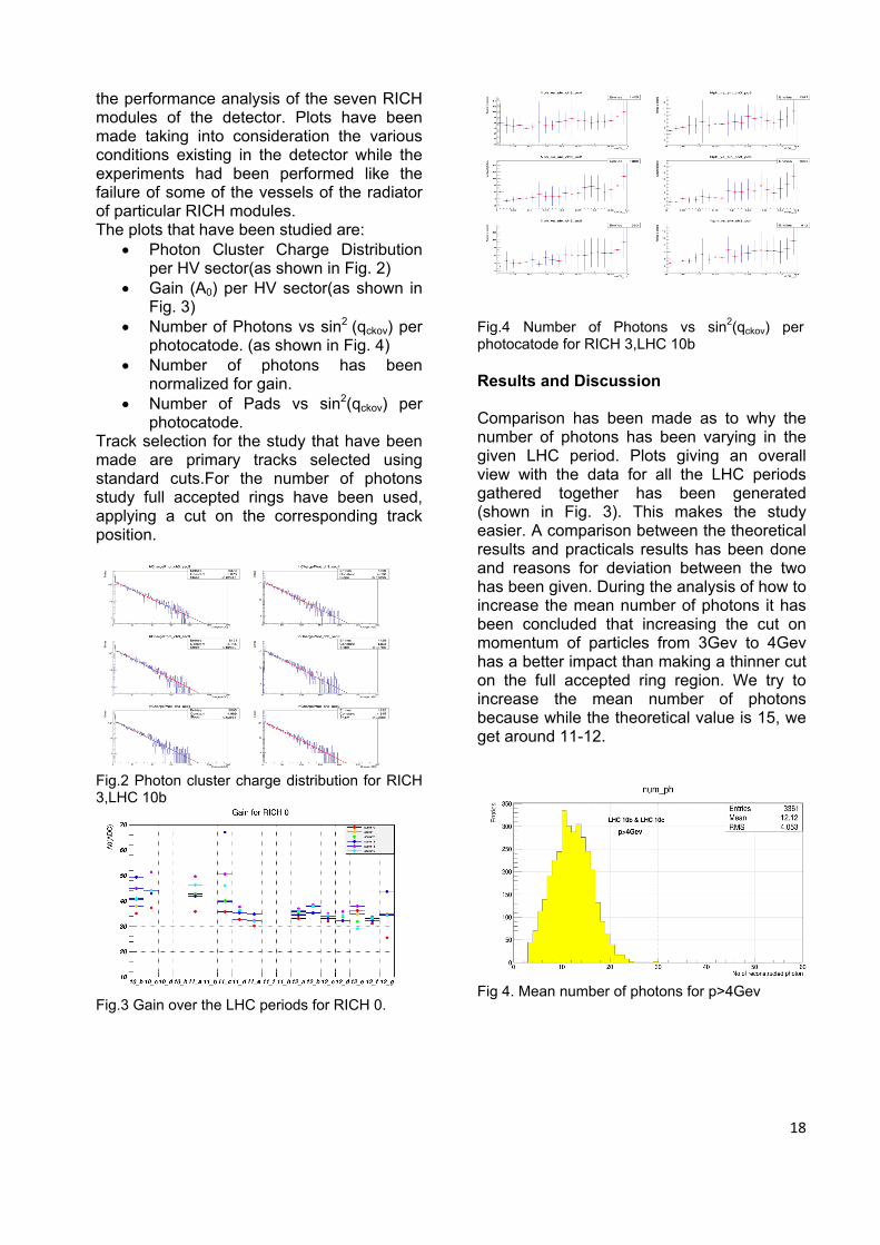
the performance analysis of the seven RICH modules of the detector. Plots have been made taking into consideration the various conditions existing in the detector while the experiments had been performed like the failure of some of the vessels of the radiator of particular RICH modules. The plots that have been studied are:
• Photon Cluster Charge Distribution per HV sector(as shown in Fig. 2)
• Gain (A0) per HV sector(as shown in Fig. 3)
• Number of Photons vs sin2 (qckov) per photocatode. (as shown in Fig. 4)
• Number of photons has been normalized for gain.
• Number of Pads vs sin2(qckov) per photocatode.
Track selection for the study that have been made are primary tracks selected using standard cuts.For the number of photons study full accepted rings have been used, applying a cut on the corresponding track position.
Fig.2 Photon cluster charge distribution for RICH 3,LHC 10b
Fig.3 Gain over the LHC periods for RICH 0.
Fig.4 Number of Photons vs sin2(qckov) per photocatode for RICH 3,LHC 10b Results and Discussion Comparison has been made as to why the number of photons has been varying in the given LHC period. Plots giving an overall view with the data for all the LHC periods gathered together has been generated (shown in Fig. 3). This makes the study easier. A comparison between the theoretical results and practicals results has been done and reasons for deviation between the two has been given. During the analysis of how to increase the mean number of photons it has been concluded that increasing the cut on momentum of particles from 3Gev to 4Gev has a better impact than making a thinner cut on the full accepted ring region. We try to increase the mean number of photons because while the theoretical value is 15, we get around 11-12.
Fig 4. Mean number of photons for p>4Gev
18

19
RESISTIVE SWITCHING OF TRANSPARENT COMPLEX OXIDE RERAM FILMS
Soumya Sarkar Fourth year B. Tech. student, Department of Electronics & Communication Engineering
National Institute of Technology Durgapur, INDIA Email id: [email protected]
NUSNNI, National University of Singapore, Singapore
May 15 – July 10, 2013
Abstract Recently there has been a lot of research in the field of finding alternatives of contemporary flash memory. One such alternative is ReRAM which functions due to the resistive switching of metal oxides between high and low resistance states on application of electric field. The main idea behind this project had been fabrication of transparent ReRAM films and investigate their V-I and R-V characteristics to determine the type of switching. Furthermore the optical properties of the device were also experimented. The fabrication of the device was done using the revolutionary PLD technique and the measurements performed using a PPMS. . Introduction In the past decade or so, advancement in the field of information technology has been magnanimous. Consequentially the need for reliable high capacity and high speed non-volatile memory devices has accelerated. Modern semiconductor nonvolatile memory have been successfully scaled to achieve high capacity memories but it is feared that in the future years this physical scaling will reach a boundary limit. An alternative is ReRAM or Resistive Random Access Memory. ReRAM technology is based on the resistive switching behavior of complex metal oxides and they have shown
promising characteristics for next generation non-volatile memory applications. Theory / Model In this project, the metal insulator transition (MIT) properties of complex metal oxides on application of electric field and their resistive switching behavior has been investigated which can be utilised as a potential for device applications. The current voltage and the resistance voltage characteristics have been analysed to determine its resistive switching behaviour. Previously a number of experiments have been carried out in this exciting field of MIT, where the transition has been electrically induced. The innovation made in this project is the use of a transparent top electrode which shall enable us to study the optical properties of the device by shining a beam of light on it and observe the change in the reflected light in response to the switching of the complex metal oxide from HRS to LRS. Experimental The device used in this project is an ITO/LAO/NSTO heterostructure fabricated using Pulsed Laser Deposition. In this method a high power pulsed laser beam inside a vacuum chamber is made to strike a target of the material to be deposited.

Fig: The ITO/LAO/NSTO sample The material or target vaporises in the form of a plasma plume and it deposits as a thin film on a substrate facing the target generally heated to an ambient temperature to grow a crystalline film. The sample was then investigated for its current voltage and resistance voltage characteristics. The sample was attached to a sample holder using a double sided tape and the two terminal connections were done using a wire bonder machine with ITO as the top electrode. Results and Discussion The characteristics of the device were tested using the Physical Properties Measurement System (PPMS) with the help of LabView program and the results were plotted using Origin 8.
Fig: Current-Voltage Characteristics
The V-I and V-R characteristics show that the nature of the ReRAM switching is unipolar.
Conclusion The main objective of this project had been to examine the possibility of resistive switching in complex metal oxide thin films with a transparent electrode, so that in future we can move towards research in the field of transparent devices with a more mature and reasonable approach. I am indebted to NUSNNI and NUS, Singapore for providing me with the support and platform to perform this project.
20

21
DESIGN AND DEVELOPMENT OF PRINTED CIRCUIT BOARDS FOR DIFFERENT CONTROLLERS OF A POWERED ORTHOSIS
Souransu Nandi
Fourth year B. Tech. student, Department of Electrical Engineering National Institute of Technology Durgapur, INDIA
Email id: [email protected]
Department of Mechanical Science and Engineering University of Illinois, Urbana - Champaign, USA
May 27 – July 31, 2013 Abstract The Human Dynamics and Controls Lab at the University of Illinois has developed a portable powered ankle foot orthosis (PPAFO) to help people walk with gait difficulties and help improve their walking capabilities. My contribution to its development was to design modular printed circuit boards that could house all the control circuitry required to operate the PPAFO without affecting the gait pattern of the patient. Introduction Walking is one of the most essential activities in the life of any healthy individual. In the United States alone, there is a considerable population of about 4.7 million people who suffer from neuromuscular impairments in the lower limbs due to polio, multiple sclerosis, cerebral palsy and spinal cord injuries. [1] An ankle foot orthosis (AFO) is a device which could aid this growing population in walking and regularizing anomalous gait (walking pattern). The PPAFO The Portable Powered Ankle Foot Orthosis (PPAFO) (Fig. 1) is a pneumatically powered device which has been developed to provide assistive dorsiflexion (toes up) and plantarflexion (toes down) torques to an ankle joint. [2] Signals from sensors on the PPAFO helps detect the different stages of gait. A microcontroller based electronic circuit is used to interpret these signals and provide
the assistive torques at the appropriate times and transmit all the data wirelessly to a computer terminal for further analysis.
Fig.1. PPAFO
My Work My work involved the study and improvement of the electrical circuit, design of 3 printed circuit boards (PCBs) to implement the control & data transmission circuitry, accommodate hardware changes and to ensure compactness of the design to provide least resistance to the natural movement of the ankle joint. Board 1 The existing control circuitry of the PPAFO based on the microcontroller MSP430G2553, had been improvised from breadboards and training kits. (Fig. 2) This assembly was bulky, prone to mechanical impacts and had to be carried by the subject on person while it was in operation. In addition presence of a

microcontroller board was unnecessary during the AFO operation. To address these issues, a customized PCB was designed to incorporate the entire control circuitry efficiently. EAGLE CAD was used to develop the schematic and the board layout.
22
Fig.2. Original Control Circuitry This PCB_1 provided a more compact, reliable, ergonomic and a modular version of the electronics. The microcontroller could be programmed separately on a different launch pad and inserted in this board for the AFO operation. Board 2 The PPAFO initially used a potentiometer based angle sensor at the ankle to record angular position during movement. However, this sensor was heavy and unwieldy for its position and hindered natural gait movements. Hence, it was replaced by a Hall Effect angle sensor. To adapt to the new hardware, the control circuitry was changed and a new board was designed on the same software platform based on the same microcontroller to facilitate the change made. This board (PCB_2) was made smaller in size and more compact than the previous one occupying a lesser volume of space when attached on the PPAFO. Board 3 An algorithm called the fractional time algorithm is being used presently for gait stage estimation. The MSP430G2553 microcontroller has a flash memory of 16kB and RAM of 500 bytes which is sufficient for executing the algorithm mentioned above.
However, algorithms such as cross correlation, nearest neighbour and particle oscillator are also to be used in the future which require more computational power and memory than the present microcontroller can provide. Hence, microcontroller TMS320F28335 was chosen for future implementation of control circuitry. TMS320F28335 boasts of a flash memory and RAM of 512kB and 68kB respectively. The TMS320F28335 control card (100 pin) can be docked on an experimenter kit for programming and signal processing. But the experimenter kit is too big to be mounted on the PPAFO without affecting gait pattern. Thus EAGLE CAD was again used to draw the schematic design and the board layout for a new PCB housing the more powerful microcontroller. Conclusion The PPAFO is a device capable of improving the standard of living of a large population today, for whom walking is an arduous task every time. Each board that has been designed has been a progress on the electronic side of the PPAFO. The PCBs have separated the programming unit and the execution unit reducing unnecessary components on the board.
Fig.3. Size comparison of the PCBs They have catered to the hardware changes and made the board as much more compact as possible. References [1] Dollar and Herr, IEEE Transactions Robotics, 24(1): 144-58, 2008 [2] KA Shorter, ET Hsiao Wecksler, GF Kogler, E Loth, WK Durfee; JRRD, vol-48, pp. 459-472, Nov 4 2011

23
MODELLING OF THE ELECTRICAL EQUIVALENT OF RESISTIVE PLATE CHAMBERS
SUDIPTO MAJUMDER
Fourth year B. Tech. student, Department of Electrical Engineering National Institute of Technology Durgapur, INDIA
Email id: [email protected]
Department of Physics CMS Collaboration, CERN, Geneva, Switzerland
May 10 – July 13, 2013 Abstract A study of the electrical equivalent of the double-gap resistive plate chambers has been presented in this paper. A systematic approach from the modelling of a single gap to a double gap RPC is performed. The equivalent circuits are modelled with the help of “Circuit Maker” software. The different components of the double gap RPC has been modelled into equivalent electrical elements that are analogous in property. Finally, a compact electrical circuit for the double gap RPC has been arrived at. The modelling has been at par with the physical working of the RPC gas gaps for the detection of muon particles in the CMS detector at CERN, Geneva. Theory An RPC is a particle detector introduced in 1981, utilising a constant and uniform electric field produced by two parallel electrode plates, at least one of which is made of a material with high bulk resistivity. A gas mixture with a high absorption coefficient for ultraviolet light is flown through the gap between the electrodes. When the gas is ionised by a charged particle crossing the chamber, free charge carriers that are deposited in the gasgap trigger avalanches of electrons in the externally applied electric field and originate a discharge. Due to the high resistivity of the electrodes, the electric field is suddenly dropped down in a limited area around the point where the discharge occurred. Thus the discharge is prevented from propagating through the whole gas volume. The propagation of the growing number of electrons induces a current on external strip electrodes. When muons pass through a chamber electrons are knocked out of the gas atoms. These electrons in turn hit outer atoms causing avalanche of electrons. Electrodes are
transparent to the signal (electrons), which are instead picked up by external metallic strips after small but precise time delay. The pattern of hit strips gives a quick measure of the muon momentum, which is then used by the trigger to make immediate decisions about whether the data are worth keeping.
Fig. A muon passing through the gas gaps, consequent avalanche of electrons and induction of charges on the readout strips by capacitive coupling Experimental Modelling The RPC gas gap consists of mainly: •Two Planer electrodes made up of Graphite. •Two Bakelite plates are separated using polycarbonate buttons shaped spacer •Fill Gas mixture •The pick-up panel composed of copper strips soldered to wires which connect to electronics. We relate each of the components with an electrical equivalent: 1. The Bakelite plates can be represented as two ohmic resistances one on both sides of the circuit. 2. The spacers are represented by an ohmic resistance. 3. The RPC gas gap ionisation volume is represented by a Zener diode.
24
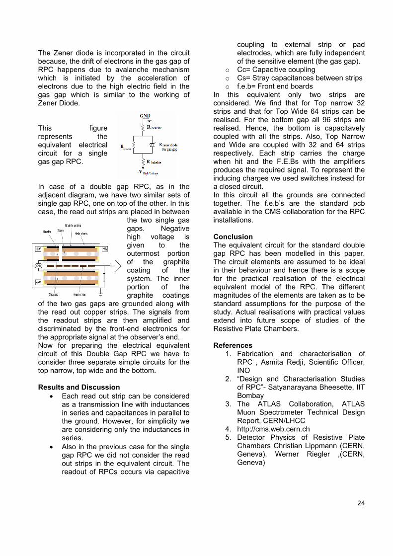
The Zener diode is incorporated in the circuit because, the drift of electrons in the gas gap of RPC happens due to avalanche mechanism which is initiated by the acceleration of electrons due to the high electric field in the gas gap which is similar to the working of Zener Diode. This figure represents the equivalent electrical circuit for a single gas gap RPC. In case of a double gap RPC, as in the adjacent diagram, we have two similar sets of single gap RPC, one on top of the other. In this case, the read out strips are placed in between
the two single gas gaps. Negative high voltage is given to the outermost portion of the graphite coating of the system. The inner portion of the graphite coatings
of the two gas gaps are grounded along with the read out copper strips. The signals from the readout strips are then amplified and discriminated by the front-end electronics for the appropriate signal at the observer’s end. Now for preparing the electrical equivalent circuit of this Double Gap RPC we have to consider three separate simple circuits for the top narrow, top wide and the bottom. Results and Discussion
• Each read out strip can be considered as a transmission line with inductances in series and capacitances in parallel to the ground. However, for simplicity we are considering only the inductances in series.
• Also in the previous case for the single gap RPC we did not consider the read out strips in the equivalent circuit. The readout of RPCs occurs via capacitive
coupling to external strip or pad electrodes, which are fully independent of the sensitive element (the gas gap).
o Cc= Capacitive coupling o Cs= Stray capacitances between strips o f.e.b= Front end boards
In this equivalent only two strips are considered. We find that for Top narrow 32 strips and that for Top Wide 64 strips can be realised. For the bottom gap all 96 strips are realised. Hence, the bottom is capacitavely coupled with all the strips. Also, Top Narrow and Wide are coupled with 32 and 64 strips respectively. Each strip carries the charge when hit and the F.E.Bs with the amplifiers produces the required signal. To represent the inducing charges we used switches instead for a closed circuit. In this circuit all the grounds are connected together. The f.e.b’s are the standard pcb available in the CMS collaboration for the RPC installations. Conclusion The equivalent circuit for the standard double gap RPC has been modelled in this paper. The circuit elements are assumed to be ideal in their behaviour and hence there is a scope for the practical realisation of the electrical equivalent model of the RPC. The different magnitudes of the elements are taken as to be standard assumptions for the purpose of the study. Actual realisations with practical values extend into future scope of studies of the Resistive Plate Chambers. References
1. Fabrication and characterisation of RPC , Asmita Redji, Scientific Officer, INO
2. “Design and Characterisation Studies of RPC”- Satyanarayana Bheesette, IIT Bombay
3. The ATLAS Collaboration, ATLAS Muon Spectrometer Technical Design Report, CERN/LHCC
4. http://cms.web.cern.ch 5. Detector Physics of Resistive Plate
Chambers Christian Lippmann (CERN, Geneva), Werner Riegler ,(CERN, Geneva)
A MULTI-AGENT TEST BED FOR MICROGRID CONTROL
Vivek Kumar Singh Fourth year B. Tech. student, Department of Electrical Engineering
National Institute of Technology Durgapur, INDIA Email id: [email protected]
Department of Electrical & Computer Science, Michigan State University, USA
July 09 –August 8, 2013
Abstract The project involves the construction of multi agent system test bed for microgrid control. It has been developed in Eclipse with Jigloo GUI builder. In the designed test bed, different computers working as agents are communicating to each other to achieve the global goal. There is no centralised computer, each computer contributing significantly to achieve the global goal. In this project, we have worked on computers having Ubuntu applications where time is synchronised by connecting to internet using NTP server. NTP is a TCP/IP protocol for synchronising time over a network. Different computers send their views in form of power, voltage and frequency. It deliberately explains the RTDS application and RSCAD software suite. Introduction The project demonstrates the application of eclipse in designing Multi Agent System. Eclipse is basically a java based open source platform that provides software developer to create a customized development environment defined as IDE which stands for Integrated Device Electronics which is a standard Electronic Interface used between computer data paths or buses. The project involves the construction of a flexible programmable Multi Agent System test bed for laboratory use. The test bed consists of 4 to 5 agents, each agent comprising a hardware controller with an embedded processor, memory and communication channel. These agents will be able to communicate with each other as well as with Real-Time Digital Simulator (RTDS) on which the power network of a microgrid can be simulated. The whole project emphasizes on decentralised Multi agent System where no single agent unilaterally commands other to achieve the main goal.
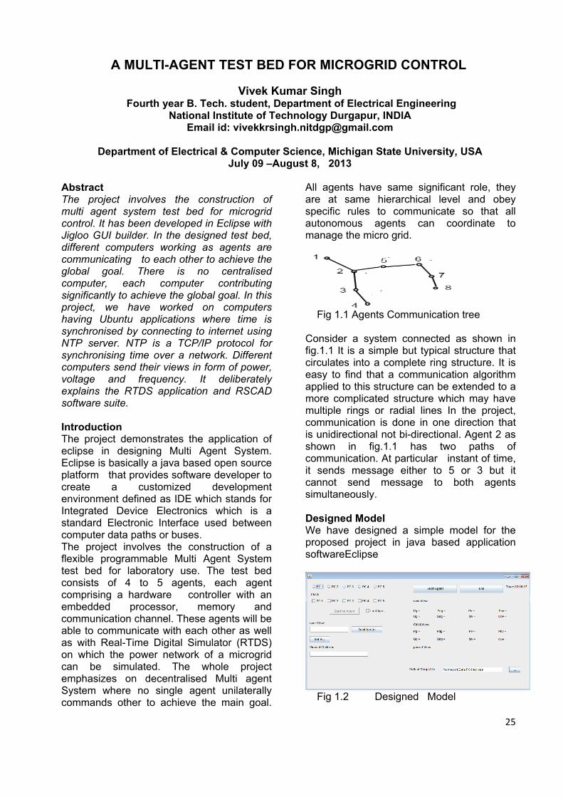
All agents have same significant role, they are at same hierarchical level and obey specific rules to communicate so that all autonomous agents can coordinate to manage the micro grid.
Fig 1.1 Agents Communication tree Consider a system connected as shown in fig.1.1 It is a simple but typical structure that circulates into a complete ring structure. It is easy to find that a communication algorithm applied to this structure can be extended to a more complicated structure which may have multiple rings or radial lines In the project, communication is done in one direction that is unidirectional not bi-directional. Agent 2 as shown in fig.1.1 has two paths of communication. At particular instant of time, it sends message either to 5 or 3 but it cannot send message to both agents simultaneously. Designed Model We have designed a simple model for the proposed project in java based application softwareEclipse
Fig 1.2 Designed Model
25

26
In the proposed design model, we have taken maximum 5 computers working as agents communicating unidirectional to achieve the global goal. There is no centralized computer, each computer contributing significantly to achieve the global goal. When PC1 working as agent is processing information at a given point of time, it is termed as current agent. If agent PC1 transmits information to agent PC2, then PC1 is called PC2’s parent agent and PC 2 is called PC1’s child agent. The Fig1.2 deliberately explains the concept of parent and child agent. Implementation & Simulation We are working on the Ubuntu installed computers where time is synchronized by connecting to internet using NTP server. NTP is a TCP/IP protocol for synchronizing time over a network. Basically a client requests the current time from a server, and uses it to set its own clock. All agents are programmed in eclipse in such a way that processing starts together irrespective of time delay. Every agents have its own views. It is basically an agent’s knowledge of system information. It consists of maximum real and reactive power generation capacity Pg, Qg, dispatchable real and reactive power generation capacity Pdg,Qdg ,vital real and reactive load demand Pv, Qv and non-vital real and reactive load demand Pnv, Qnv in the designed model. In the mentioned project, we have defined a class called script .java where we have defined different parameters of power, frequency, voltage and time (ms) with values to get different readings .The input script file is written in Ms Excel where frequency is increasing to 1decimal unit for every 5 sec. Clock Design in Eclipse During project, we have to design a clock with label in order to initiate the communication of different computer simultaneously and to calculate the lagging time between different agents. We defined a class called setting. When we type some
texts in the text field and press the button, text is written into a file. The file is a simple text file which stores the information of path of workspace where data have been saved earlier. When I start the program again, it should read automatically the text in the file and print it in the same text field. We have checked box which determines whether the file is checked or not. Conclusion The proposed project is a modern approach to comprehensive control strategy of micro grid. The proposed project utilizes the concept of power control strategy to different computers working as agents in order to design multi agent system test bed. It deliberately explains the RTDS application and RSCAD software suite. It demonstrates the views of different agents working together to achieve the global goal using different parameters and mathematical values. It also demonstrate the application of agent tool III in multi agent system engineering which can play a significant role in future while designing multi agent system test bed. Acknowledgement I would like to give my sincere thanks to research committee of NIT Durgapur for providing financial assistance to carry out the summer project in foreign university. I would like to express my great appreciation to Prof. Joydeep Mitra for his patient support, valuable and continuous guidance throughout the project. I would like to thank Mohammed Ben-Idris and Niannian Cai for keeping me motivated all the time during the project and making me feel comfortable with the new environment. My grateful thanks are also extended to Mrs. Pauline Vandyke for assisting me in getting identity card and activating my account and Mrs. Jennifer Woods for providing me the keys and access to ERISE summer lab.

27
SEMANTIC WEB-BASED E-COUNSELING SYSTEM
Anish Singhania Fourth year B. Tech. student, Department of Information Technology
National Institute of Technology Durgapur, INDIA Email id: [email protected]
pp. 70-74, Proceedings of International Multi-Conference on Software, Electronics,
Communication and Mechanical Engineering (IMSECME'12), Dec. 29 -30, 2012, Kuala Lumpur (Malaysia)
Abstract Presently on Internet, it is difficult to find a resource which serves as one-stop destination for students regarding their career-related queries. Students who use Internet to search for help end up with large amount of information, mostly irrelevant. This happens because of current syntax-based web search which just matches words of the query and returns all string-matched results. Thus, this research work proposes a Semantic web-based e-counseling system. It captures the query from the student in Natural Language, understands the logic of the query and returns a reply just as a human counselor would, which helps the student to find a proper career option with less efforts and time. The Natural Language Query is parsed by a NLP Parser to form a data structure which is compared to the Ontology, a hierarchical set of concepts and relations of a domain, and only relevant options are presented to the student. Introduction and System Overview In general, in an e-counseling system, a student is required to enter his choice of subject and field of interest in a form-based enquiry and a huge amount of data, both relevant and irrelevant, is returned to the student as a result. These results are not entirely according to the student’s need as the form prevents the student from completely expressing itself. The vast expanse of data available on the web further adds to the woe. The proposed system gives a real-life counselor-like reasoning and logical capability to the searching mechanism. The student now can enter a query according to its own needs and get a result that it wants.
This allows the student to interact more with the system and hence a lot more queries are asked and results returned, in contrast to the form-based system wherein the extent of the queries is limited. This is the concept that is underlying the Semantic Web Technology. The proposed idea uses forms a hierarchy of the available data, dividing them into classes and relating them through properties (relations) so that they can be semantically searched through Ontology. Now, the student queries to the system and the system forms a semantic hierarchy of the query after parsing the query and compares it with the ontology to return a result. The system helps the student by reasoning the question so that all the relevant results are returned. For example: If a student queries for ‘Computer Science and Technology’, all results elated to ‘Computer’ and ‘Computer Science’ will also be returned, helping the student by returning logical results. Implemented System Architecture A. Interface A web-based medium between the user and the underlying semantic search system that accepts a query in Natural Language to be processed .The query is processed by the underlying system and finally the result is displayed. Therefore, the interface helps the user interact with the system. B. NLP parser Parser is a Java-based tool used to parse natural language query and to analyse the grammatical structure of the sentence. It groups together words to form phrases and resolves the different dependencies into various parts of speech. It parses the input in various output formats and saves the resultant output in a .txt or .xml file.
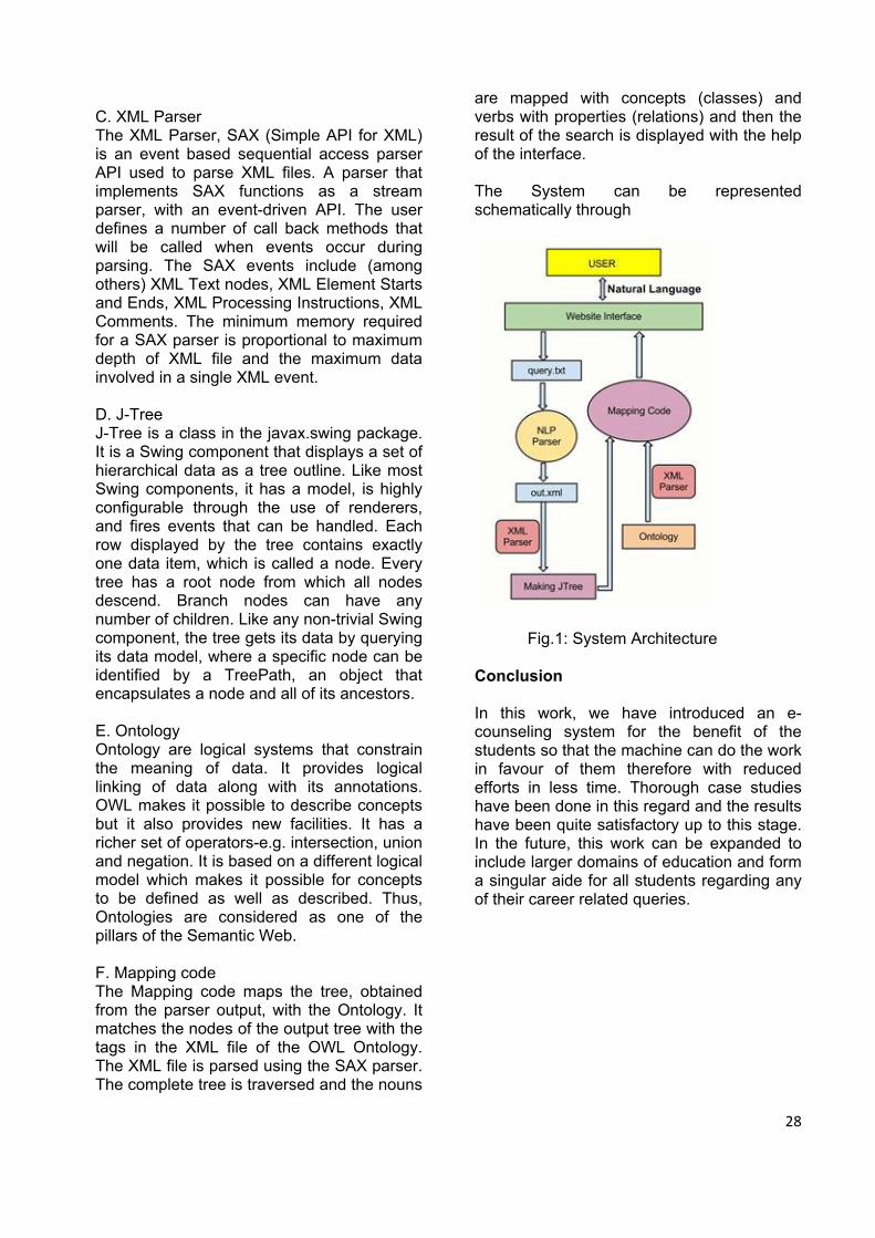
C. XML Parser The XML Parser, SAX (Simple API for XML) is an event based sequential access parser API used to parse XML files. A parser that implements SAX functions as a stream parser, with an event-driven API. The user defines a number of call back methods that will be called when events occur during parsing. The SAX events include (among others) XML Text nodes, XML Element Starts and Ends, XML Processing Instructions, XML Comments. The minimum memory required for a SAX parser is proportional to maximum depth of XML file and the maximum data involved in a single XML event. D. J-Tree J-Tree is a class in the javax.swing package. It is a Swing component that displays a set of hierarchical data as a tree outline. Like most Swing components, it has a model, is highly configurable through the use of renderers, and fires events that can be handled. Each row displayed by the tree contains exactly one data item, which is called a node. Every tree has a root node from which all nodes descend. Branch nodes can have any number of children. Like any non-trivial Swing component, the tree gets its data by querying its data model, where a specific node can be identified by a TreePath, an object that encapsulates a node and all of its ancestors. E. Ontology Ontology are logical systems that constrain the meaning of data. It provides logical linking of data along with its annotations. OWL makes it possible to describe concepts but it also provides new facilities. It has a richer set of operators-e.g. intersection, union and negation. It is based on a different logical model which makes it possible for concepts to be defined as well as described. Thus, Ontologies are considered as one of the pillars of the Semantic Web. F. Mapping code The Mapping code maps the tree, obtained from the parser output, with the Ontology. It matches the nodes of the output tree with the tags in the XML file of the OWL Ontology. The XML file is parsed using the SAX parser. The complete tree is traversed and the nouns
are mapped with concepts (classes) and verbs with properties (relations) and then the result of the search is displayed with the help of the interface. The System can be represented schematically through
Fig.1: System Architecture Conclusion In this work, we have introduced an e-counseling system for the benefit of the students so that the machine can do the work in favour of them therefore with reduced efforts in less time. Thorough case studies have been done in this regard and the results have been quite satisfactory up to this stage. In the future, this work can be expanded to include larger domains of education and form a singular aide for all students regarding any of their career related queries.
28

29
MODELLING OF MULTIAGENT BASED RAILWAY SYSTEM
USING BDI LOGIC
Ankit Bhardwaj M. Tech Second year student, Department of Information Technology
National Institute of Technology Durgapur, INDIA Email id: [email protected]
International Conference on future trends in computing and communication-FTCC 2013
Bangkok, Thailand July 13-July 14, 2013
Abstract Multi-Agent based modeling & simulation is an evolving paradigm for solving real life problems for solving real life problems for the last one decade. In this paper, we model the manually controlled Indian Railway to a multi agent based automated system which is robust in nature and provide a fully automated collision avoidance guarantee. We consider individual entity such as station, junction and train as an agent and the whole railway network is framed as a graph. To sharpen the solutions of existing system´s problems such as collisions and delays, BDI agent with first order predicate logic is incorporated in this paper. The communication and coordination between respective agents (with help of their BDI and rule base running as backbone) can now be a substitution in place of manual decisions. Thus the idea can replace the hectic job of railway control room personals in more sophisticated & methodical way. Introduction Railway system is the biggest public transportation in the world which is used to provide better transportation service to the public than private one. There are lots of advantages of using the public transport such as lesser fuel consumption, convenience, lesser fare, lesser pollution and many more. But in parallel with these advantages the existing railway system has some disadvantages also like Collisions and delays and unfortunately they are more dangerous and lossy than private transport. Railway is a distributed system which can be efficiently modelled by the intelligent agents. A Software Agent [1] is essentially a special software component that has autonomy to
provide an inter-operable interface to an arbitrary system. A Multiagent system (MAS) [2] is a group of agents, which interact with each other and negotiate in a decision to achieve a common goal. MAS can be empowered with the help of BDI theory. BDI is a philosophical and mental model for multiagent based problems. Railway system is a Socio-Technical system which can be modeled by BDI agent [7] using three words Belief, Desire and Intension. During his lifetime an agent go though in following working loop depicted in Fig:1 :
Fig. 1: Working principle of BDI Now apart from the BDI theory we are going to concatenate first order predicate logic in this paper which empowers the railway model many times. The combination of mathematical logic and BDI theory gives stronger solution for railway system problems because the logic gives precise meaning to mathematical statements. System Model • System Architecture We define railway system by following tuples set:Rsys = < G, A> Where, G is a Graph representation of railway tracks and stations. A is a set of agents deployed on the graph.(Figure: 2) Now the graph G can be defined as G = < V, E > Where, V is the set of vertices and E is the set of directed edges. Again, V = S U J

S = Si | i=1,2….n Si ϵ S represents a station node with an unique id i And J = Ji | i=1,2….m Ji ϵ J represents a junction node with an unique id i J = x | x ϵ V, and Capacity(x)=1 and Waiting_on(x)=0 In the graph of this system model we are considering the directed edges so trains can move in these directions only . Eijk = Vi → Vj And E = Eijk | Vj = AdjG(Vi) Here AdjG(Vi) is a adjacency function which determines the adjacent nodes of Vi . As there may be more than one edge between Vi to Vj , to uniquely define each edge between Vi to Vj we define Eij as Eijk. Where k = 1, 2….e and e is the total number of edges directed from Vi to Vj . Now the another parameter of the system model is A (agent), A = SA U JA U TA Where SA = SAi | i=1,2….n SAi ϵ SA represents a Station Agent with an unique id i which is static in nature. JA = JAi | i=1,2….m JAi ϵ JA represents a Junction Agent with an unique id i which is static in nature. In our system model a train agent can be defined by the following attributes, TAi : <ID,R,ST,WT,MPS> Where, ID = Unique id of the train agent TAi. R[i][j] is List of stations that TAi must follow as its Route and j = 1, 2…. n , while n is the total number of stations in the route of TAi. ST[i][j] is Schedule time of TAi in the jth station (R[i][j]),WT[i][j] is Waiting time of TAi in the jth station (R[i][j]), MPS is Maximum permissible speed of TAi. Similarly SAj: <ID,Capacity,LT,AS,Edge> And JAk : <ID,LT,AS,Edge,B> Where, ID is Unique id of the respective agent, Capacity is maximum number of trains SAj can hold at a time, LT[p] is List of trains those left SAj or JAk but still not reached to the next stop, AS[p] is List of adjacent stations of SAj or JAk, Edge[p] is List of outgoing edges of SAi. • BDI Architecture of System To differentiate among tags of BDI, we give
the following well defined structure to represent belief, desire and intension. The predicates and functions which we use frequently to define the BDI of a agent are summarized in Table: I. 1) Belief Logic Tags: <B A Belief1> Here < > is used to denote the tags. First character of tag can have three possible characters B, D and I which denote the tag type. B is used for Belief tags. Second character of the tag contains agent id. In above belief tag, we put the agent id A, who has the state of environment Belief1 as belief. 2) Desire Logic Tags: <D A Desire1> Similarly, here D denotes the tag type that is desire and A denotes the agent id. The above tag denotes that agent A has desire Desire1. Like <D TA1 CurrentSpeed(MPS)> tag denotes that TA1 has a desire to gain the MPS. 3) Intension Logic Tags: <I A Intension1> Intension is a desire with commitment to fulfill it. So the difference between the Intension and desire tag is tag type symbol only. Rest parts of the tag remain same for an intension tag of a agent like desire tag. Conclusion In this paper we propose a BDI logic based modeling of railway system which gives a strong foundation to solve the problems of existing railway system and also gives an autonomous shape to it. Our proposed model promotes the utilization of predicate logics with multi agent system to enhance the quality of service of the system. In a concise form we can state that this paper is directed to develop a BDI agent based autonomous railway system (with the rule base as a backbone) which can overcome the fallacy of manual intervention and human dependency. The future prospect of this work will be simulate the whole network with JADE (which is a Java based agent oriented tool) by using the real dataset collected from the Asansol division of Eastern Railways, India which can give the flavour of real time simulation.
30
31
EFFECT OF ANNEALING ON YELLOW ORANGE PHOTOLUMINESCENCE EMISSION OF UNCAPPED Mn2+ DOPED ZnS QUANTUM DOTS SYNTHESIZED BY SIMPLE CHEMICAL METHOD
Arup Kanti Kole
Ph D student, Nanoscience Laboratory, Department of Physics National Institute of Technology Durgapur, INDIA
Email id: [email protected]
7th International Conference on Materials for Advanced Technologies Suntec, Singapore, June 30-July 05, 2013
Abstract Amongst others doped ZnS nanomaterials, Mn2+-doped ZnS quantum dots (QDs) have promising applications in optoelectronic devices. Annealing treatments are also very common in semiconductor processing and can be used to improve the crystal quality and to confirm the stability of the crystal, which is important for device fabrication. However, in this work synthesis of uncapped 40.0 mol% Mn2+ doped ZnS QDs of average sizes ~2.5nm in de-ionized (DI) water medium at room temperature (RT) is reported. The particle size is confirmed by Transmission Electron Microscope (TEM) and X-ray diffraction (XRD) studies. Unannealed samples show dual PL emission peak, one centred at 400 nm assigned due to recombination between the sulphur vacancy related donor and zinc vacancy related acceptor levels, other at yellow-orange region, centred at 600nm assigned due to partially allowed 4T1-6A1 transition of Mn2+ in ZnS. The XRD patterns show that the transformation from cubic ZnS to wurtzite ZnO phase has taken place at 6000C temperature. There are various reports of Mn2+ PL emission enhancement by annealing, but in the present experiment, for the first time, we have observed that the intensity of Mn2+ related yellow-orange emission peak decreases continuously with the increase of the annealing temperature. The reduction of yellow-orange PL emission intensity might have taken place due to the diffusing out of Mn2+ dopant from the ZnS lattice during annealing.
Introduction Out of various II-VI semiconductor QDs, ZnS has attracted a lot of attention due to its wide direct band gap (3.68eV at room temperature), large exciton binding energy (~40meV) and potential application in solar cell, flat panel display, sensor, laser and photocatalytic dye degradation etc. By doping transition metal ion such as Ag2+, Co2+, Cu2+, Mn2+ etc. in ZnS semiconductor QDs, the UV-Vis optical absorption and PL emission properties can be tuned easily and makes it a promising material for its application in various optoelectronic devices where tenability is required. Another important technique to obtain efficient and tuned PL emission from semiconductor QDs is the thermal annealing. Such annealing treatments are widely used in semiconductor processing to improve the crystal quality and to confirm the stability of the crystal, which is important for device fabrication. In the present work we have reported the effect of thermal annealing at 100-6000C temperature range on structural and PL emission properties of uncapped ZnS and ZnS:Mn QDs of average sizes~2-3nm synthesized by simple chemical precipitation method at RT. Experimental ZnS QDs and Mn2+ (40 mol%) doped ZnS QDs are synthesized at RT by simple chemical co-precipitation method in DI water medium. All the chemicals used are of AR grade (Merck and SD fine chemicals, Mumbai) and are used without further purification. For the synthesis of ZnS QDs, zinc nitrate is dissolved in DI water. After 1 h of continuous stirring, sodium sulphide solution in DI water is added drop-wise into

32
the zinc nitrate solution. After 1 h continuous stirring of the reaction mixture, the precipitate is then separated by centrifugation. For the synthesis of Mn2+ doped ZnS QDs, manganese acetate dissolved in DI water is mixed with the zinc nitrate solution. After 1h continuous stirring of the reaction mixture, sodium sulphide solution is added drop-wise and it is again stirred continuously for another 1h. Finally the precipitate is collected by centrifugation and dried in RT for further measurements. The samples are then heated at the rate of 100C/min for 1 h and held for 2 h at four different temperatures of 100, 200, 400, and 6000C in a muffle furnace. Then the samples are cooled at the rate of 100C/min (furnace cooling). The samples are then collected for further measurements. Results and Discussion The UV-Vis absorption spectra of the annealed samples show a red shift with increasing annealing temperature due to the increase in particle size as a result of annealing which is further confirmed from TEM image analysis. XRD data analysis show that upto 4000C annealing temperature, the crystallinity of the samples increases as the annealing temperature increases and at 6000C temperature, cubic ZnS has converted to wurtzite ZnO. We have studied the effect of annealing on the PL emission spectra. For undoped ZnS, only one PL emission peak at 400nm can be observed where as for Mn2+ doped ZnS QDs, in addition to this peak another yellow-orange emission peak at 600nm can be observed. The UV emission is assigned due to recombination between the sulphur vacancy related donor and zinc vacancy related acceptor levels. When Mn2+ ions are doped in ZnS, it occupies the sites of Zn2+ and the mixing between the s–p electrons of the host ZnS and the d electrons of Mn2+ occurs and made the forbidden 4T1-6A1 transition partially allowed and it results Mn2+ related yellow-orange PL emission. The UV emission peak present in both undoped and Mn2+ doped ZnS samples at first increases with increase in annealing temperature upto 2000C due to the improved crystallinity as observed from XRD analysis and it decreases at 4000C temperature may be due to the removal of
the defect at this temperature. Further it increases at 6000C and it corresponds to the strong excitonic emission of ZnO as observed earlier by other researchers for ZnO QDs. There are various reports of Mn2+
PL emission enhancement by annealing, but in the present experiment, for the first time, we have observed that the intensity of Mn2+ related yellow-orange emission peak decreases continuously with the increase of the annealing temperature. The reduction of yellow-orange PL emission intensity might have taken place due to the diffusing out of Mn2+ dopants from the ZnS lattice during annealing. Further increase in particle size due to annealing beyond the ‘quantum confinement’ regime leads to weak interaction between the d electronic state of Mn2+ and the s-p electronic state of host ZnS leading to a decrease in yellow-orange PL emission intensity. Conclusion Synthesis of ZnS and Mn2+ doped ZnS QDs of sizes ~2-3nm at RT by using simple chemical precipitation method without using any capping agent is reported. The effect of annealing on RT PL emission spectra of Mn2+ doped ZnS QDs have been studied in detail and it shows continuous decrease in PL emission intensity with increasing annealing temperature. This decrease in PL emission intensity has been attributed to the diffusing out of Mn2+ dopant in ZnS during annealing. The yellow-orange emission as observed from Mn2+ doped ZnS QDs show that it can be used in future optoelectronic devices Acknowledgement I am thankful to my thesis supervisor, Dr. P. Kumbhakar, Professor, Dept. of Physics, NIT Durgapur for providing me the opportunity for this visit. I also acknowledge Department of Science and Technology (DST), GOI, and NIT Durgapur, India for providing the Air fare, visa fee, registration fee etc. References [1] R.N.Bhargava, D.Gallagher, X.Hong, A.Nurmikko, Phys. Rev. Lett. 72, 416 (1994). [2] A.K.Kole, C.S.Tiwary, P.Kumbhakar, J. Appl. Phys. 113, 114308 (2013). [3] D.Son, D.Jung, J.Kim, T.Moon, C.Kim, B.Park, Appl. Phys. Lett. 90, 101910(2007).
A FAMILY OF FLEXIBLE OFFSET-TIME BASED WAVELENGTH SCHEDULERS FOR OBS EDGE-NODES
Bikash Choudhury
M. Tech Second year student, Department of Information Technology National Institute of Technology Durgapur, INDIA
Email id: [email protected]
IEEE 3rd International Conference on Photonics - ICP 2012 Pulau Pinang, Malaysia, Oct 01-03, 2012
Abstract A family of variable offset-time based wavelength scheduling schemes for OBS edge-nodes, is proposed which performs 4-20 times better than ordinary LAUC-VF schedulers in terms of byte loss rate (ByLR). The schedulers accept a minimum and a maximum limit of offset-time along with the length of the burst as input and then return the appropriate wavelength and the exact offset-time, to be used for the burst. The basic principle is to align the burst either at the beginning or at the end of an existing void so that no new void is created after scheduling the burst unless mandated by the offset-time limits. Introduction Since its inception, optical burst switching (OBS) technology has attracted the attention of networking community throughout the world and now it is being considered as a very promising technology towards implementation of all-optical Internet in near future. OBS combines the advantageous features of optical circuit switching (OCS) and optical packet switching (OPS) techniques by elegantly separating control plane functionalities from data plane. Statistical multiplexing gain (SMG), slightly lower than that offered by OPS, can be derived without processing the packets electronically. Data packets from a source to a destination can be forwarded all-optically without requiring optical/electrical/optical (O/E/O) conversion at the intermediate nodes. Moreover, in doing so, the SMG is just marginally compromised.
33
we propose a scheduling scheme for edge OBS nodes, where the offset-time is allowed to be variable within a given range and the
exact (within the given range) offset-time is decided by the scheduler itself. In the existing schemes, the scheduler is provided with the rigid offset-time(t0) and burst-length(B) of the new (to be scheduled) burst. The scheduler has to search for the voids in each channel that can hold the burst and then according to a scheduling criterion, the appropriate wavelength is selected. But, in our approach, the scheduler is provided with the burst-length and a lower limit(tmin) and an upper limit(tmax) of offset-times. The scheduler then returns a wavelength (λ), at which the burst should be scheduled and also an offset-time (t0) within the given range. The basic difference between our approach and existing approaches is illustrated in Fig.2.
Fig. 2: Existing and Proposed approach The Proposed Scheme The basic objective of our approach is to minimize the number of voids by concatenating the new burst with an existing burst if possible (meeting the offset-time constraints) so that no new void is created after scheduling the new burst. This can be done in various ways. One possible way is to search the void of maximum length among the contending wavelengths within the given range of offset-time and then scheduling the new burst either at the beginning or at the end of the void. We term this scheme as max-void variable offset-time scheduling. In this scheme, we have two variations - the
new burst can be scheduled at the beginning or at the end of the maximum void. We term them as max-void-min-offset scheduler and max-void-max-offset scheduler respectively. Both the schemes give significant loss reduction compared to that obtained from existing schemes but the schemes are likely to favour burst of smaller size compared to burst of larger size, that may arrive in future. General Framework: We define a slot as a two tuple vector (t; s) where t denotes the start-time of the slot and s denotes the state (empty or occupied) of the slot. Note that s can assume either 0 if the slot is void (empty) or 1 if the slot is occupied. Thus state of an wavelength w can be represented as an ordered sequence of slots. For convenience of computation, we assume that the start-time of the first slot is always zero and the state of the last slot (actually the void at the end) is always zero. Thus state of w can be represented as w=(0,s1), (t2,s2),.., (th,0) ----(1) where th is termed as the horizon of the channel. Now, we define the max-voids and min-voids for the schemes as follows vmax1 = maxi,jvij,V vij ϵ V1 ---(2) vmax2 = maxi,jvij,V vij ϵ V2, provided tmin≤tB≤tmax ---(3) vmin1 = mini,jvij,V vij ϵ V1 ---(4) vmin2 = mini,jvij,V vij ϵ V2, provided tmin≤tB≤tmax ---(5) An additional constraint, as mentioned above, on (4) and (5) is that vij≥ B + Bmin
The Schemes 1) Max-Void based Schemes: First, we outline the steps involved in the max-void-min-offset scheduler as below a) Search vmax1 within the link and return the wavelength in which vmax1 occurs. b) Return the start-time of vmax1 as the offset-time to be used for the new burst. 2) Min-Void based schemes: A criticism to the above schemes is that as the new burst is scheduled at the vmax1 or vmax2, the algorithm will gradually reduce the size of vmax1 or vmax2 and bursts of larger lengths will never have a chance to be scheduled. So, we study a diametrically opposite scheduling scheme, named as min-void variable offset-time scheduling, as follows:
a)Find vmin1 and schedule the burst at the wavelength to which vmin1 belongs. The value of vmin1 should be at least equal to (B + Bmin). b) Return offset-time, equal to the start-time of the void vmin1. At this point, we analyze the complexity of the proposed schemes. Let, W be the number of wavelengths available per link then complexity of LAUC-VF is O(W) i.e. it has to make W number of comparisons before scheduling the burst. Our proposed schemes have to search the min-void or max-void over all wavelengths within the limits tmin and tmax. If the average burst length is B’, then number of voids in the link is O(W(tmax - tmin)=B’) and hence the complexity of the proposed scheme is O(W2(tmax- tmin)=B’). Results and Discussions: The results obtained for various schemes from above studies are shown together in Fig.2 for average burst-duration of 90 µs considering the 2 hop topology as discussed. above.
Fig2: ByLR for LAUC-VF, Max-Void, Min-Void and Mod-max with average burst duration = 90_s and hops = 2 Conclusions and Future Scope We propose two scheduling schemes that place the burst within the void of maximum size. Max-void-min-offset-time scheme schedules the burst at the beginning of the maximum void whereas max-void-max-offset-time scheme schedules the burst at the end of the max-void. The ByLR performance of max-void-min-offset-time scheme is found to be better than the other scheme and compared to LAUC-VF, it performs 4 to 20 times better, based on average burst-length and applied load. Then a scheme is proposed where the burst is scheduled at the beginning of the minimum-void in the link.
34
35
CHAOTIC BLOCK ENCRYPTION WITH POSITION PERMUTATION
Debanjana Baksi M. Tech 2011-13, Department of INFORMATION TECHNOLOGY
National Institute of Technology Durgapur, INDIA Email id: [email protected]
pp. 71-77, Proceedings of International Conference on Advances in Computing and
Communications Technologies, Pattaya, Thailand, January 19-20, 2013 Abstract Chaotic encryption method is becoming increasingly popular in real-time image encryption/ decryption systems for its high security, speed, computational overheads. But it is not possible to generate pure random numbers (true chaotic sequence) using finite-state machines such as digital computers and dynamical degradation creeps in. This paper reports that the security falls off in chaotic encryption systems due to dynamical degradation, from systems which use 32 bits to generate chaos, to systems which use 8 bits for the same, and becomes insecure in the case of systems which use 8 bits. The paper also proposes a new algorithm based on block based two layer permutations of pixels, which works on systems using 8 bits to generate chaos, enhancing its security level. The resultant cipher has been found to be resistant to known attacks. A comparison in terms of some well defined metrics such as correlation co-efficient, NPCR and UACI is also done.
Keywords: chaos, image encryption, dynamical degradation, confusion and diffusion, NPCR, UACI. Introduction Chaos based image encryption schemes have been increasingly studied to meet the demand for real-time secure image transmission over the internet and wireless networks. The development of chaos theory began in the1960s (and established in 1970s) with efforts from many different research areas (the pioneering research on chaos may be retrospected to H. Poincaré’s work in 1890s, when he found the complexity of three-body celestial system), such as mathematics , physics, biology, chemistry
etc. [Stewart, 1990]. Some researchers have pointed out the tight relationship among chaos, communication security and cryptography. Many fundamental characteristics of chaos, such as the ergodicity, mixing and exactness property and the sensitivity to initial conditions can be connected to the properties of “confusion” and “diffusion” in cryptography. So it is natural to use chaos to enrich the design of new ciphers. Experimental In this work, a block based chaotic cipher system has been proposed. This generates chaos using 8 bit numbers and employs two level pixel permutations to create confusion. Final encrypted image is obtained using pixel by pixel XOR operation between the plaintext & chaotic sequence. This algorithm achieves the desired properties of confusion and diffusion and provides good resistance to common attacks. An experiment has been performed to obtain the output of logistic map with 8 bit initial condition. It is observed that the output does not show sufficient sensitivity to initial condition. Figures 2(a) to 2(c) show how the difference in the plot of the output of logistic map, with two slightly different 8 bit initial conditions, shows periodicity. Thus chaotic ciphers where 8 bit initial conditions are used to generate chaos show less key sensitivity. This is illustrated in figure 3(a)-(c).

Fig 3 (a) Lena image encrypted with key 11100001 (b) Lena image decrypted with key 11100001 (same key) (c) Lena image decrypted with key 11100000 (different key) Results and Discussion A good encryption technique should be robust against cryptanalytic, statistical and brute-force attacks. The security analysis of the proposed encryption scheme has been performed extensively such as statistical analysis, key sensitivity analysis, plain image sensitivity analysis and key space analysis to prove the security level of the algorithm. After obtaining highly positive results in each section it can be inferred that the proposed algorithm is highly resistive against brute-force attacks and histogram analysis establishes its robustness against any statistical attack.
Conclusion A novel chaotic image encryption technique is proposed. The new technique is capable of reducing dynamical degradation. The encryption algorithm uses a 128 bit key (16 characters) to encrypt a 256 × 256 image and it is highly sensitive to the initial condition. Most importantly the scheme has been designed in such a way that it works successfully when chaos is generated using 8 bits. The map does not lose its chaotic behaviour. Its computational complexity is also very low and it has a large key space at the same time. The proposed algorithm is highly resistive against brute-force attacks and histogram analysis establishes its robustness against any statistical attack. The obtained results show the superiority of the proposed scheme.
36
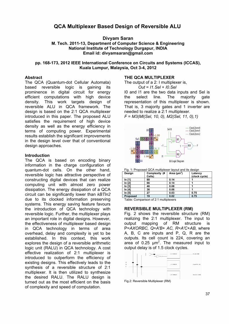
QCA Multiplexer Based Design of Reversible ALU
Divyam Saran M. Tech. 2011-13, Department of Computer Science & Engineering
National Institute of Technology Durgapur, INDIA Email id: [email protected]
pp. 168-173, 2012 IEEE International Conference on Circuits and Systems (ICCAS),
Kuala Lumpur, Malaysia, Oct 3-4, 2012 Abstract The QCA (Quantum-dot Cellular Automata) based reversible logic is gaining its prominence in digital circuit for energy efficient computations with high device density. This work targets design of reversible ALU in QCA framework. The design is based on the 2:1 QCA multiplexer introduced in this paper. The proposed ALU satisfies the requirement of high device density as well as the energy efficiency in terms of computing power. Experimental results establish the significant improvements in the design level over that of conventional design approaches. Introduction The QCA is based on encoding binary information in the charge configuration of quantum-dot cells. On the other hand, reversible logic has attractive perspective of constructing digital devices that can realize computing unit with almost zero power dissipation. The energy dissipation of a QCA circuit can be significantly lower than kBTln2 due to its clocked information preserving systems. This energy saving feature favours the introduction of QCA technology with reversible logic. Further, the multiplexer plays an important role in digital designs. However, the effectiveness of multiplexer based design in QCA technology in terms of area overhead, delay and complexity is yet to be established. In this context, this work explores the design of a reversible arithmetic logic unit (RALU) in QCA technology. A cost effective realization of 2:1 multiplexer is introduced to outperform the efficiency of existing designs. This effectively leads to the synthesis of a reversible structure of 2:1 multiplexer. It is then utilized to synthesize the desired RALU. The RALU design is turned out as the most efficient on the basis of complexity and speed of computation.
THE QCA MULTIPLEXER The output of a 2: I multiplexer is,
Out = I1.Sel + I0.Sel I0 and I1 are the two data inputs and Sel is the select line. The majority gate representation of this multiplexer is shown. That is, 3 majority gates and 1 inverter are needed to realize a 2:1 multiplexer. F = M3(Ml(Sel, 10, 0), M2(Sel, 11, 0),1)
Fig. 1: Proposed QCA multiplexer layout and its design Design Complexity (#
Cells) Area (µm2) Latency
(clock cycle) In [1] 88 0.14 1 In [2] 66 0.14 1 In [3] 46 0.08 1 In [4] 36 0.06 1 In [5] 27 0.03 0.75 Proposed 19 0.02 0.75 Table: Comparison of 2:1 multiplexers REVERSIBLE MULTIPLEXER (RM) Fig. 2 shows the reversible structure (RM) realizing the 2:1 multiplexer. The input to output mapping of RM structure is P=AXORBC, Q=A'B+ AC, R=A'C+AB, where A, B, C are inputs and P, Q, R are the outputs. Its cell count is 224, covering an area of 0.25 µm2. The measured input to output delay is of 1.5 clock cycles.
Fig.2: Reversible Multiplexer (RM)
37

REVERSIBLE ALU (RALU) A major application of the reversible multiplexer is the design of reversible ALU (RALU). The components of an RALU are the reversible logic unit (RLU), a reversible arithmetic unit (RAU) and an RM gate which selects either output from the RLU or RAU. Reversible logic unit (RLU) A 4:1 multiplexer can act as an I-bit Logic Unit if its data inputs are used as controls and the select lines as two 1-bit inputs of the ALU (Fig. 3). The design has 6 garbage outputs. The QCA implementation of the design requires only 3 RM gates, and consequently uses 30 MVs and has an overall delay of 3 clock cycles (12 clock zones).
Fig. 3: Reversible Logic Unit (RLU) Table: Functionalities of RLU Reversible arithmetic unit (RAU) A full adder can act as an arithmetic unit if one of the two data lines is controlled. Fig.4 is a 5-input and 2-output circuit with 6 garbage outputs realizing an RAU. The QCA implementation of the RAU also requires 40 MV s with a delay of 6 clock cycles. RALU is
a 6-input and 2-output circuit with 20 garbage outputs. QCA implementation of RALU require 8 RM gate and consequently
38
require 80 MVs. For page limitation, QCA cell layouts and its simulation results of RLU, RAU and RALU, and the schematic diagram of RALU are not given here.
Fig.4: Reversible Arithmetic Unit (RAU)
Table: Functionalities of RAU Conclusion In this work architecture of a 2:1 multiplexer around QCA (quantum-dot cellular automata) is introduced considering the primitives (majority voter). The resulting design consists of 19 cells covering an area of 0.02 µm2 which is substantially lower than that of existing designs. It adds to significant improvements in QCA logic circuit design. A reversible multiplexer is then synthesized to explore the design of an efficient reversible ALU (RALU), in QCA, that out performs the performance of existing designs. References 1. K. Kim, K. Wu, R. Karri, 'The Robust QCA Adder Designs Using Composable QCA Building Blocks' 2. V. Mardiris, Ch. Mizas, L. Fragidis and V. Chatzis, 'Design and simulation of a QCA 2 to 1 multiplexer' 3. T. Teodsio and L. Sousa. 'QCA -LG: A tool for the automatic layout generation of QCA combinational Circuits' 4. S. Hashemi, M.R. Azghadi, A. Zakerolhosseini, 'A novel QCA multiplexer design' 5. A. Roohi, H. Khademolhosseini, S. Sayedsalehi, 'A Novel Architecture For QCA'
C0 C1 C2 C3 PO Result 0 0 0 0 0 - 0 0 0 1 A.B AND 0 0 1 1 B COPY 0 1 0 1 A COPY
0 1 1 0 A XOR B XOR
0 1 1 1 A+B OR 1 0 0 0 (A+B)' NOR
1 0 0 1
A EXNOR B EQUAL
1 0 1 0 A' NOT 1 1 0 0 B' NOT 1 1 1 0 (A.B)' NAND 1 1 1 1 1 CONSTANT
C0 C1 C2 PO FUNCTION 0 0 0 A Transfer A 0 0 1 A+1 Increment A 0 1 0 A+B Addition 0 1 1 A+B+1 Addition with carry
1 0 0 A+B 1's complement Subtraction
1 0 1 A+B+1 2's complement Subtraction
1 1 0 A-1 Decrement A 1 1 1 A Transfer A

39
AGENT BASED TASK SPECIfiC TEAM FORMATION FOR EFFECTIVE DISTRIBUTED DECISION MAKING
Arambam James Singh
M Tech Second Year, Department of Information Technology, National Institute of Technology Durgapur, INDIA
Email : [email protected]
pp. 1-6, Proceedings of 10th International Conference(IEEE) on Electrical Engineering/Electronics, Computer, Telecommunications and Information Technology
(ECTI-CON), Krabi, Thailand, May 15-17, 2013 Abstract Getting solution of a problem by group discussion is more reliable than getting solution from a single entity. To increase reliability of the solution, efficient group of experts should be formed. Here in this paper we have proposed a methodology for finding efficient team of experts for solution of a given problem collaboratively. The methodology is conceptualized with the notion of Multiagent system. We have considered several factors like Cardinality of team, ability, willingness, trust and reciprocality of an agent in order to construct the team. We have also proposed an optimization function which will be used to choose most eligible agents to form the team of experts. Introduction In order to get an effective solution of a given problem, a team of expert agents should be formed in which all the members are very much capable and willing as well as highly trustable. If the number of team members is very large, then the cost of decision making increases as large number of message passing is required but reliability of solution increases however if number of team memb- er is less, then cost decreases but reliability also decreases. So to form a team with maximum reliability of solution and minimum cost, an optimum team size should be choosen. Theory / Model Let A = Ai | i ε[1,n] is a pool of agent. And Suniv = Sj | j ε [1,m] be the universal set of skills which are required to perform any task in a particular domian. Each agent Ai
where i ε [1,n] has it’s own skill set SAi Suniv
in their Knowledge Base(KB). Now suppose from a user U , a problem P comes to an agent Ai ε A and suppose Ai identifies the required skill set to solve the problem. As it doesn’t have the identified skill set in it’s KB, it cannot solve it. Thus it forward the skill set to it’s neighbouring agents for a collaborative solution and initiate the request for Team Formation. Now we have to build a group of
expert agents Gf A which will collaboratively
provide an effective solution of the given problem P. Suppose from a user U a problem P of domain dmi comes to an agent Ai for solution. Let Ai is not capable of finding the solution as required skill sets are not in it’s knowledge base(KB). So agent Ai as a task provider starts finding a team of expert agents who can collaboratively make the solution from pool of agents in domain dmi. Finding a team of experts can be done in two phases, • Phase 1 : Initial Group Formation • Phase 2 : Final Group Formation A. Phase 1 : Initial Group Formation Initially from pool of agents number of expert agents are selected to form a group Gi. The group should satisfy the following criterias:- 1) Wav is maximum: Average Willingness of the Group should be maximum. It can only be
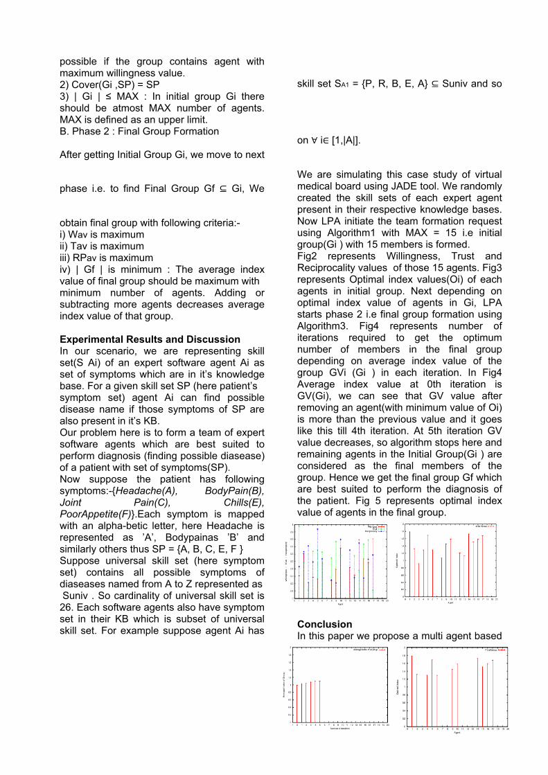
possible if the group contains agent with maximum willingness value. 2) Cover(Gi ,SP) = SP 3) | Gi | ≤ MAX : In initial group Gi there should be atmost MAX number of agents. MAX is defined as an upper limit. B. Phase 2 : Final Group Formation After getting Initial Group Gi, we move to next
phase i.e. to find Final Group Gf Gi, We
obtain final group with following criteria:- i) Wav is maximum ii) Tav is maximum iii) RPav is maximum iv) | Gf | is minimum : The average index value of final group should be maximum with minimum number of agents. Adding or subtracting more agents decreases average index value of that group. Experimental Results and Discussion In our scenario, we are representing skill set(S Ai) of an expert software agent Ai as set of symptoms which are in it’s knowledge base. For a given skill set SP (here patient’s symptom set) agent Ai can find possible disease name if those symptoms of SP are also present in it’s KB. Our problem here is to form a team of expert software agents which are best suited to perform diagnosis (finding possible diasease) of a patient with set of symptoms(SP). Now suppose the patient has following symptoms:-Headache(A), BodyPain(B), Joint Pain(C), Chills(E), PoorAppetite(F).Each symptom is mapped with an alpha-betic letter, here Headache is represented as ’A’, Bodypainas ’B’ and similarly others thus SP = A, B, C, E, F
40
Suppose universal skill set (here symptom set) contains all possible symptoms of diaseases named from A to Z represented as Suniv . So cardinality of universal skill set is 26. Each software agents also have symptom set in their KB which is subset of universal skill set. For example suppose agent Ai has
skill set SA1 = P, R, B, E, A Suniv and so
on i [1,|A|].
We are simulating this case study of virtual medical board using JADE tool. We randomly created the skill sets of each expert agent present in their respective knowledge bases. Now LPA initiate the team formation request using Algorithm1 with MAX = 15 i.e initial group(Gi ) with 15 members is formed. Fig2 represents Willingness, Trust and Reciprocality values of those 15 agents. Fig3 represents Optimal index values(Oi) of each agents in initial group. Next depending on optimal index value of agents in Gi, LPA starts phase 2 i.e final group formation using Algorithm3. Fig4 represents number of iterations required to get the optimum number of members in the final group depending on average index value of the group GVi (Gi ) in each iteration. In Fig4 Average index value at 0th iteration is GV(Gi), we can see that GV value after removing an agent(with minimum value of Oi) is more than the previous value and it goes like this till 4th iteration. At 5th iteration GV value decreases, so algorithm stops here and remaining agents in the Initial Group(Gi ) are considered as the final members of the group. Hence we get the final group Gf which are best suited to perform the diagnosis of the patient. Fig 5 represents optimal index value of agents in the final group.
Conclusion In this paper we propose a multi agent based

41
team formation mechanism for a task considering parameters like cardinality of team, willingness, ability, trust and reciprocality of the agent. We also propose an optimization function which evaluates the final team members. Effectiveness of theteam is determined by the average willingness, trust and reciprocality of the team as a whole. Fig 2 Fig3 Fig 4 Fig5

42
SUPPLIER SELECTION IN RISK ENVIRONMENT: FUZZY INTERVAL
TYPE-2 TOPSIS METHOD
Pritha Das M.Tech 2011-13, Department of Mathematics
National Institute of Technology Durgapur, INDIA Email id: [email protected]
pp. 16-21, Proceedings of International Conference on Advances in Computing and
Communications Technologies, Pattaya, Thailand, January 19-20, 2013 Abstract An application of unequal weighted fuzzy multi-attribute decision making method based interval type-2 TOPSIS method on supplier selection in a risk oriented supply chain is discussed. Eight risks evaluative attribute namely, Performance risk, Demand risk, Environmental risk, Process risk and Logistics risk are taken for selecting among three supplier alternatives. The above fuzzy based Interval type-2 Topsis method remarkably reduce the degree of computation in constructing the average decision matrix and weighted decision matrix of attributes enhancing Lee and Chen’ ranking value approach of trapezoidal interval type-2 fuzzy sets in selection of alternatives. The result is consistent, rational, and inventive and practically proved useful in choosing better suppliers alternatives in risky supply chain environment. Keywords -- Interval type-2 fuzzy sets, TOPSIS method, ranking weighted decision matrix, supply chain risk management. Introduction In recent years, supply chain has become more complicated and widespread. As the organization becomes more dependent on multi- suppliers, poor decision making process will lead to excessive delays in manufacturing and poor customer service. In this paper the supplier selection problem in supply chain takes into account various risk factors like demand risk, Performance risk, Environmental risk, Process risk and Logistics risk, from supplier
side, properly maintaining manufacturer quality level and delivery schedule. The overall objective of the selection is to identify the least risky supplier from the given alternatives based on decisions of the expert Decision makers from different fields. In the process of decision making, due to vague human nature the information of weights of the attributes and alternatives relative to these attributes are given in linguistic terms. In this paper, we focus our attention on issue of selection of Tyre Manufacturing companies in supply chain under uncertain fuzzy environment, applying interval type-2 TOPSIS method. Experimental We consider three Commercial Tyres Manufacturer companies, in Indian market, as alternatives, namely “Apollo Tyres” (x1), “MRF Tyres” (x2), “CEAT Tyres” (x3) and five risk attributes. The three decision makers (D1) (Production Manager), (D2) (Economist/statistical analyst), (D3) (Chemical Engineer) use the linguistic terms shown in Table 1, to represent the risk attributes weights, shown in Table 2 and evaluating values of different alternatives against different risk attributes shown in Table 3.

Results and Discussion By implementing the aforesaid algorithm with MATLAB, we have come obtained the order of risky behavior of the companies as follows:
x₁>x₃>x₂
The quantitative result obtained is shown.
Conclusion In this paper, we have presented algorithmic model for fuzzy multiple group decision making (FMCDM) based on interval type-2 TOPSIS method. Using this approach decision makers can derive attributes weights and alternatives weights for total ranking indices and find the least risky supplier from given alternatives easily. In the case study, we have constructed the decision matrices and weighting decision matrices based on trapezoidal interval type -2 fuzzy sets and then present ranking based on ranking values. In future, the proposed algorithmic approach can be applied in other fields as image processing, machine learning, critical medical diagnosis, pattern recognition, solving fuzzy relation equations, function approximation, equalization of non-linear fading channels, forecasting of time series etc.
43

44
2-Π CROSSTALK NOISE MODEL FOR DEEP SUBMICRON VLSI GLOBAL RC INTERCONNECTS
Saupayan Mazumdar
Fourth year B. Tech. student, Department of Electronics and Communication Engineering National Institute of Technology Durgapur, INDIA
Email id: [email protected]
2013 IEEE Conference on Electronics Systems, Designs and Applications (ICEDSA) Kuala Lumpur, Malaysia
November 05- November 06, 2012 Abstract In today’s high performance IC design noise estimation and avoidance are becoming very important issues. This paper presents a much improved, highly accurate and efficient noise model called 2-π model for the accurate estimation of crosstalk noise. The proposed model incorporates all the physical properties including victim and aggressor drivers, distributed RC characteristics of interconnects and coupling locations of both victim and aggressor lines. Then with the help of this model, expressions for peak noise and noise width as well as sensitivity expressions to all model parameters are calculated. We then use these sensitivity expressions to analyze and evaluate various noise avoidance techniques. Introduction The rapid advances in VLSI technology has resulted in the reduction of feature size which affects the crosstalk noise problem and also affects the design’s timing and functionality goals [1-2]. This reduction in chip area results in the performance degradation of VLSI circuits (eg: logic failure, unwanted coupling voltage between two adjacent wires, timing delay etc.) Theory / Model For simplicity, we first explain 2-π model for the case where the victim net is a RC line. For a victim net with some aggressor nearby, let the aggressor voltage pulse at the coupling location be a saturated ramp input with transition time being tr and the interconnect length of the victim net before
the coupling location, at the coupling location and after the coupling be Ls, Lc and Le, respectively. The 2-π type reduced RC model is generated is shown.
Experimental
NOISE AVOIDANCE TECHNIQUES A. Driver Sizing Driver sizing can help to reduce the peak crosstalk noise, since a strong driver is more capable to sustain a noise spike. Our model does indicate some situation under which increasing driver size (i.e., reduce Rd) may help to reduce the peak noise. It also indicates the situation under which increasing driver size may not help to reduce the peak noise. B. Wire Spacing Wire spacing is another way which can reduce the maximum noise and noise width,

with an area penalty. For a wire of fixed width, its coupling capacitance decreases while its ground capacitance increases, as its spacing to a neighbor wire increases. On the other hand, coupling capacitance of the wire increases while ground capacitance decreases, when its spacing to a neighbor wire decreases. C. Wire Sizing Wire sizing is another factor which can be used for maximum noise and noise width reduction. As the wire’s width is decreased, its resistance increases and its ground capacitance decrease. On the other hand, as the wire’s width is increased its resistance decreases and its ground capacitance increases. D. Noise Amplitude-Width Product The effective way to reduce amplitude-width (AW) product are wire spacing, driver sizing and wire sizing which helps in reducing noise. A receiver may still be noise immune even the peak noise exceeds certain threshold voltage. This can be explained with the help of amplitude (A) versus width plots, which can then be transformed into amplitude (A) versus amplitude-width (AW) product (A-AW) plots. Results and Discussion
45
We have generated 150 random circuits using the parameter ranges presented in Section 2 and 3 and looked at the sensitivity of noise peak to each model parameter. The units are mV/fF for capacitances and mV/Ω for resistances. Figure 3 shows the scatter diagram comparing the 2- π model (y-axis) with HSPICE (x-axis) simulations for 150 randomly generated four-pin nets. HSPICE simulations are performed on distributed RC networks by dividing each long wire into every 100μm segment. The average errors for peak noise and noise width are 3.43% and 5.23%, respectively. Table-1 gives the comparative result of the peak noise voltage and noise width computed using SPICE and the proposed method. The peak noise obtained from the analytical model is compared to SPICE in terms of the physical separation between the signal line and the shield line, as shown in Figure 4. Figure 4 shows the coupling noise for shielded
interconnect decreases with increase in the physical separation between the signal line and the shield line. When the signal width increases, the resistance of the aggressor is reduced and the coupling noise increases as shown in Figure 5. The ground capacitance of the victim line also increases, however, causing the coupling noise to decrease.
Conclusion This paper presents improved 2-π crosstalk noise model and various noise avoidance techniques for RC on-chip VLSI interconnects. Error presented by this model is less than 5% on average compared with SPICE simulation, for both peak noise voltage and noise width estimation. Results show that the average error for noise peak is 2.2 % and for the width is 5.2% while allowing for very fast analysis. The proposed model can be used to allow time-efficient accurate analysis of multi conductor line structures.