supersedes j-std-001ds september 2006 joint industry · pdf filejoint industry standard space...
TRANSCRIPT
JOINTINDUSTRY
STANDARD
Space Applications
Electronic Hardware
Addendum to
J-STD-001D
Requirements for
Soldered Electrical
and Electronic
Assemblies
Amendment 1
J-STD-001DSAmendment 1September 2009
Supersedes J-STD-001DSSeptember 2006

The Principles ofStandardization
In May 1995 the IPC’s Technical Activities Executive Committee (TAEC) adopted Principles ofStandardization as a guiding principle of IPC’s standardization efforts.
Standards Should:• Show relationship to Design for Manufacturability
(DFM) and Design for the Environment (DFE)• Minimize time to market• Contain simple (simplified) language• Just include spec information• Focus on end product performance• Include a feedback system on use and
problems for future improvement
Standards Should Not:• Inhibit innovation• Increase time-to-market• Keep people out• Increase cycle time• Tell you how to make something• Contain anything that cannot
be defended with data
Notice IPC Standards and Publications are designed to serve the public interest through eliminating mis-understandings between manufacturers and purchasers, facilitating interchangeability and improve-ment of products, and assisting the purchaser in selecting and obtaining with minimum delay theproper product for his particular need. Existence of such Standards and Publications shall not inany respect preclude any member or nonmember of IPC from manufacturing or selling productsnot conforming to such Standards and Publication, nor shall the existence of such Standards andPublications preclude their voluntary use by those other than IPC members, whether the standardis to be used either domestically or internationally.
Recommended Standards and Publications are adopted by IPC without regard to whether their adop-tion may involve patents on articles, materials, or processes. By such action, IPC does not assumeany liability to any patent owner, nor do they assume any obligation whatever to parties adoptingthe Recommended Standard or Publication. Users are also wholly responsible for protecting them-selves against all claims of liabilities for patent infringement.
IPC PositionStatement onSpecificationRevision Change
It is the position of IPC’s Technical Activities Executive Committee that the use and implementationof IPC publications is voluntary and is part of a relationship entered into by customer and supplier.When an IPC publication is updated and a new revision is published, it is the opinion of the TAECthat the use of the new revision as part of an existing relationship is not automatic unless requiredby the contract. The TAEC recommends the use of the latest revision. Adopted October 6, 1998
Why is therea charge forthis document?
Your purchase of this document contributes to the ongoing development of new and updated industrystandards and publications. Standards allow manufacturers, customers, and suppliers to understandone another better. Standards allow manufacturers greater efficiencies when they can set up theirprocesses to meet industry standards, allowing them to offer their customers lower costs.
IPC spends hundreds of thousands of dollars annually to support IPC’s volunteers in the standardsand publications development process. There are many rounds of drafts sent out for review andthe committees spend hundreds of hours in review and development. IPC’s staff attends and par-ticipates in committee activities, typesets and circulates document drafts, and follows all necessaryprocedures to qualify for ANSI approval.
IPC’s membership dues have been kept low to allow as many companies as possible to participate.Therefore, the standards and publications revenue is necessary to complement dues revenue. Theprice schedule offers a 50% discount to IPC members. If your company buys IPC standards andpublications, why not take advantage of this and the many other benefits of IPC membership aswell? For more information on membership in IPC, please visit www.ipc.org or call 847/597-2872.
Thank you for your continued support.
©Copyright 2009. IPC, Bannockburn, Illinois, USA. All rights reserved under both international and Pan-American copyright conventions. Anycopying, scanning or other reproduction of these materials without the prior written consent of the copyright holder is strictly prohibited andconstitutes infringement under the Copyright Law of the United States.
J-STD-001DS
Space Applications
Electronic Hardware
Addendum to J-STD-001D
Requirements for
Soldered Electrical and
Electronic Assemblies
Amendment 1
Developed by the Space Electronic Assemblies J-STD-001 AddendumTask Group (5-22as) of the Assembly & Joining Processes Committee(5-20) of IPC
Users of this publication are encouraged to participate in thedevelopment of future revisions.
Contact:
IPC3000 Lakeside Drive, Suite 309SBannockburn, Illinois60015-1249Tel 847 615.7100Fax 847 615.7105
Supersedes:J-STD-001DS - November 2006
ASSOCIATION CONNECTINGELECTRONICS INDUSTRIES ®

AcknowledgmentMembers of the Space Electronic Assemblies J-STD-001 Addendum Task Group have worked together to develop thisdocument. We would like to thank them for their dedication to this effort. Any document involving a complex technologydraws material from a vast number of sources. While the principal members of the Space Electronic Assemblies J-STD-001Addendum Task Group (5-22as) of the Assembly & Joining Processes Committee (5-20) are shown below, it is not possibleto include all of those who assisted in the evolution of this standard. To each of them, the members of the IPC extend theirgratitude.
Assembly & JoiningProcesses Committee
Space Electronic AssembliesJ-STD-001 Addendum Task Group
Technical Liaisons of theIPC Board of Directors
ChairLeo P. LambertEPTAC Corporation
ChairGarry D. McGuireNASA Marshall Space Flight Center
Peter BigelowIMI Inc.
Sammy YiAptina Imaging Corporation
Space Electronic Assemblies J-STD-001 Addendum Task Group
Teresa, Rowe, AAI Corporation
Helen, Ting, Aerojet
Bill, Strachan, ASTA - PortsmouthUniversity
Greg, Hurst, BAE SYSTMS
Marvin, Banks, Ball Aerospace &Technologies
Thomas, Carroll, Boeing - IntegratedDefense Systems
Karl, Mueller, Boeing Company
Mary, Bellon, Boeing SatelliteDevelopment Center
Helena, Pasquito, Cobham DefenseElectronic Systems
Daniel, Foster, Defense AcquisitionInc.
Theodore, Edwards, Dynaco Corp.
Leo, Lambert, EPTAC Corporation
Stephen, Fribbins, Fribbins TrainingServices
Anthony, Monteiro, HamiltonSundstrand
Doug, Rogers, Harris Corporation,GCSD
William, Blackwood, HoneywellAerospace Electronic Systems
John, Mastorides, HoneywellAerospace Electronic Systems
Hector, Valladares, HoneywellAerospace Electronic Systems
Richard, Rumas, Honeywell Canada
Riley, Northam, HoneywellTechnology Solutions Inc.
Jennie, Hwang, H-TechnologiesGroup
John Kirk, Bonner, Jet PropulsionLaboratory
Reza, Ghaffarian, Jet PropulsionLaboratory
Kim, Phillips, Jet PropulsionLaboratory
Alan, Young, Jet PropulsionLaboratory
Joel, Weiner, Johns HopkinsUniversity
Norma, Moss, L-3 Communications
Blen, Talbot, L-3 Communications
Vijay, Kumar, Lockheed MartinMissile & Fire Control
Sam, Polk, Lockheed Martin Missilesand Fire Control
Michael, Green, Lockheed MartinSpace Systems Company
Hue, Green, Lockheed Martin SpaceSystems Company
Jeffery, Luttkus, Lockheed MartinSpace Systems Company
Kelly, McCarrie, Lockheed MartinSpace Systems Company
James, Moffitt, Moffitt ConsultingServices
Arthur, Hayhurst, NASA
Leonard, Hee, NASA Ames ResearchCenter
Howard, Trent, NASA Dryden FlightResearch Center
Ronald, Hebden, NASA GoddardSpace Flight Center
Robert, Humphrey, NASA GoddardSpace Flight Center
Jeannette, Plante, NASA GoddardSpace Flight Center
Robert, Cooke, NASA Johnson SpaceCenter
Anthony, Wong, NASA JohnsonSpace Center
James, Blanche, NASA MarshallSpace Flight Center
Charles, Gamble, NASA MarshallSpace Flight Center
Garry, McGuire, NASA MarshallSpace Flight Center
Tim, White, NASA Stennis SpaceCenter
Kirk, Armstrong, NAVAIRAISD
Mahendra, Gandhi, NorthropGrumman Aerospace Systems
Ge, Wang, Northrop GrummanAerospace Systems
Randy, McNutt, Northrop GrummanCorp.
William, Rasmus, NorthropGrumman SSES
September 2009 J-STD-001DS - Amendment 1
iii
Matt, Garrett, Phonon Corporation
Michael, Blige, Raytheon Company
Robert, Dennis, Raytheon Company
Philip, Henault, Raytheon Company
Lisa, Maciolek, Raytheon Company
David, Nelson, Raytheon Company
William, Ortloff, Raytheon Company
Patricia, Pittman, Raytheon Company
Fernando, Salinas, RaytheonCompany
Donna, Spruill, Raytheon Company
Bill, Starmann, Raytheon Company
Fonda, Wu, Raytheon Company
Montey, Collins, Raytheon MissileSystems
Kathy, Johnston, Raytheon MissileSystems
Royston, Lewinson, Raytheon MissileSystems
Rosa, Miranda, Raytheon MissileSystems
Joseph, Schmidt, Raytheon MissileSystems
Leticia, Vasquez, Raytheon MissileSystems
Patrick, Kane, Raytheon SystemTechnology
Bryan, James, Rockwell Collins
Terry, Clitheroe, Solder Technologies
Roger, Bell, Space Systems/Loral
Mel, Parrish, STI Electronics
Patricia, Scott, STI Electronics
Michael, Engler, The AerospaceCorporation
Sharon, Ventress, U.S. Army Aviation& Missile Command
Kirk, Armstrong, U.S. Navy
Lori, Watts, U.S. Navy
Dominic, LaPinta, United SpaceAlliance
J-STD-001DS - Amendment 1 September 2009
iv

Space Applications Electronic HardwareAddendum to J-STD-001D Requirements for
Soldered Electrical and Electronic Assemblies
0.1 SCOPE
This addendum provides requirements to be used in addi-tion to, and in some cases, in place of, those published inIPC J-STD-001D to ensure the reliability of soldered elec-trical and electronic assemblies that must survive the vibra-tion and thermal cyclic environments getting to and oper-ating in space. See Table 1 clause 1.1 Scope.
0.1.1 Purpose When required by procurementdocumentation/drawings, this Addendum supplements orreplaces specifically identified requirements of IPC J-STD-001, Revision D of February 2005. See Table 1 clause 1.2Purpose.
0.1.2 Precedence The contract takes precedence overthis Addendum, referenced standards and user-approveddrawings (see IPC J-STD-001 D 1.7.1). In the event of aconflict between this Addendum and the applicable docu-ments cited herein, this Addendum takes precedence.Where referenced criteria of this addendum differ from thepublished IPC J-STD-001D, this addendum takes prece-dence. See Table 1 clauses 1.7 Order of Precedence and1.7.1 Conflict.
0.1.3 Existing or Previously Approved Designs ThisAddendum shall not constitute the sole cause for the rede-sign of previously approved designs. When drawings forexisting or previously approved designs undergo revision,they should be reviewed and changes made that allow forcompliance with the requirements of this Addendum.
0.1.4 Use This addendum is not to be used as a stand-alone document.
Where criteria are not supplemented, the Class 3 require-ments of IPC J-STD-001D apply. If an IPC J-STD-001Drequirement is changed or added by this Addendum, theclause is listed in J-STD-001DS Table 1 Space Applica-tions Requirements and the entire IPC J-STD-001Dclause is replaced by this addendum except as specificallynoted.
The clauses modified by this Addendum do not includesubordinate clauses unless specifically stated (e.g., 1.4 doesnot include 1.4.1). Clauses, Tables, Figures, etc., in IPCJ-STD-001D that are not listed in this addendum are to beused as-published.
0.1.5 Lead-Free Tin For the purpose of this document,lead-free (Pb-free) tin is defined as tin containing less than3 percent lead by weight as an alloying constituent. Solderalloy Sn96.3Ag3.7 is exempt from this requirement. SeeTable 1, clause 3.2.
0.1.6 Use of Lead-Free Tin The use of components,assemblies, packaging technology, mechanical hardware,and materials meeting any of the following conditions shallbe prohibited unless documented and controlled through aUser approved Lead-Free Control Plan (LFCP) incorporat-ing either a replating or hot solder dip (HSD) process thatcompletely replaces the lead-free tin finish, or a minimumof two mitigation measures.
• Pb-free Tin platings, metallization, etc on external sur-faces of parts, mechanical parts etc., or in internal cavitysurfaces (i.e.: hybrid, relay crystal cans, MEMS etc).
• Any components, CCAs etc., assembled with Pb-free Tinsolder alloys except Sn96.3 Ag3.7 (see paragraph 3.2).
0.1.6.1 Lead Free Control Plan The Lead Free ControlPlan (LFCP) shall document controls and processes thatassures that assemblies containing Lead-free Tin solderalloys and/or component finishes will perform as intendedwithin the expected parameters of the mission, e.g., envi-ronment, duration, etc. At a minimum, the LFCP shall:
a. Document every incidence of Lead-free Tin technologyand prevent its use without review and approval by theUser prior to implementation.
b. Incorporate a minimum of two mitigation measureswhen the Lead-free Tin finish is not completely replacedthrough a replating or HSD process.
c. Include any special design requirements, mitigationmeasures, test and qualification requirements, qualityinspection and screening, marking and identification,maintenance, and repair processes.
d. Require review and approval by the User prior to imple-mentation.
The following documents may be helpful when developingthe LFCP:
• GEIA-STD-0005-1, Performance Standard for Aerospaceand High Performance Electronic Systems ContainingLead-free Solder
• GEIA-STD-0005-2, Standard for Mitigating the Effects ofTin Whiskers in Aerospace and High Performance Elec-tronic Systems
September 2009 J-STD-001DS - Amendment 1
1
• GEIA-HB-0005-1, Program Management/Systems Engi-neering Guidelines For Managing The Transition ToLead-Free Electronics
• GEIA-HB-0005-2, Technical Guidelines for Aerospaceand High Performance Electronic Systems ContainingLead-free Solder and Finishes
• GEIA-STD-0006, Requirements for Using Solder Dip toReplace the Finish on Electronic Piece Parts
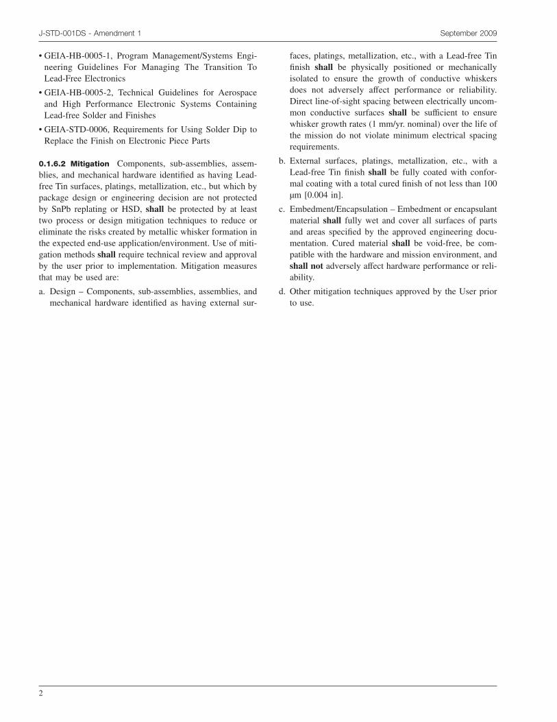
0.1.6.2 Mitigation Components, sub-assemblies, assem-blies, and mechanical hardware identified as having Lead-free Tin surfaces, platings, metallization, etc., but which bypackage design or engineering decision are not protectedby SnPb replating or HSD, shall be protected by at leasttwo process or design mitigation techniques to reduce oreliminate the risks created by metallic whisker formation inthe expected end-use application/environment. Use of miti-gation methods shall require technical review and approvalby the user prior to implementation. Mitigation measuresthat may be used are:
a. Design – Components, sub-assemblies, assemblies, andmechanical hardware identified as having external sur-
faces, platings, metallization, etc., with a Lead-free Tinfinish shall be physically positioned or mechanicallyisolated to ensure the growth of conductive whiskersdoes not adversely affect performance or reliability.Direct line-of-sight spacing between electrically uncom-mon conductive surfaces shall be sufficient to ensurewhisker growth rates (1 mm/yr. nominal) over the life ofthe mission do not violate minimum electrical spacingrequirements.
b. External surfaces, platings, metallization, etc., with aLead-free Tin finish shall be fully coated with confor-mal coating with a total cured finish of not less than 100µm [0.004 in].
c. Embedment/Encapsulation – Embedment or encapsulantmaterial shall fully wet and cover all surfaces of partsand areas specified by the approved engineering docu-mentation. Cured material shall be void-free, be com-patible with the hardware and mission environment, andshall not adversely affect hardware performance or reli-ability.
d. Other mitigation techniques approved by the User priorto use.
J-STD-001DS - Amendment 1 September 2009
2
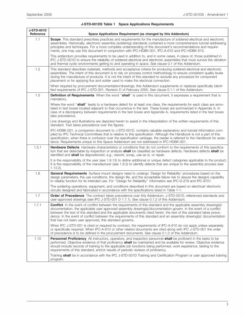
J-STD-001DS Table 1 Space Applications Requirements
J-STD-001DReference Space Applications Requirement (as changed by this Addendum)
1.1 Scope This standard prescribes practices and requirements for the manufacture of soldered electrical and electronicassemblies. Historically, electronic assembly (soldering) standards contained a more comprehensive tutorial addressingprinciples and techniques. For a more complete understanding of this document’s recommendations and require-ments, one may use this document in conjunction with IPC-HDBK-001, IPC-A-610 and IPC-HDBK-610.
This addendum provides requirements to be used in addition to, and in some cases, in place of, those published inIPC J-STD-001D to ensure the reliability of soldered electrical and electronic assemblies that must survive the vibrationand thermal cyclic environments getting to and operating in space. See clause 0.1 of this Addendum.
1.2 This standard describes materials, methods and acceptance criteria for producing soldered electrical and electronicassemblies. The intent of this document is to rely on process control methodology to ensure consistent quality levelsduring the manufacture of products. It is not the intent of this standard to exclude any procedure for componentplacement or for applying flux and solder used to make the electrical connection.
When required by procurement documentation/drawings, this Addendum supplements or replaces specifically identi-fied requirements of IPC J-STD-001, Revision D of February 2005. See clause 0.1.1 of this Addendum.
1.5 Definition of Requirements When the word ‘‘shall’’ is used in this document, it expresses a requirement that ismandatory.
Where the word ‘‘shall’’ leads to a hardware defect for at least one class, the requirements for each class are anno-tated in text boxes located adjacent to that occurrence in the text. These boxes are summarized in Appendix A. Incase of a discrepancy between requirements in the text boxes and Appendix A, requirements listed in the text boxestake precedence.
Line drawings and illustrations are depicted herein to assist in the interpretation of the written requirements of thisstandard. Text takes precedence over the figures.
IPC-HDBK-001, a companion document to J-STD-001D, contains valuable explanatory and tutorial information com-piled by IPC Technical Committees that is relative to this specification. Although the Handbook is not a part of thisspecification, when there is confusion over the specification verbiage, the reader is referred to the Handbook for assis-tance. Requirements unique to this Space Addendum are not addressed in IPC-HDBK-001.
1.5.1 Hardware Defects Hardware characteristics or conditions that do not conform to the requirements of this specifica-tion that are detectable by inspection or analysis shall be classified as hardware defects. Hardware defects shall beidentified and shall be dispositioned, e.g., rework, scrap, use as is, or repair.
It is the responsibility of the user (see 1.8.13) to define additional or unique defect categories applicable to the product.It is the responsibility of the manufacturer (see 1.8.5) to identify defects that are unique to the assembly process (see1.13.2).
1.6 General Requirements Surface mount designs need to undergo ‘Design for Reliability’ procedures based on thedesign parameters, the use conditions, the design life, and the acceptable failure risk to assure the designs capabilityto reliably function for its intended use. For ‘‘Design for Reliability’’ information see IPC-D-279 and IPC-9701.
The soldering operations, equipment, and conditions described in this document are based on electrical/ electroniccircuits designed and fabricated in accordance with the specifications listed in Table 1-1.
1.7 Order of Precedence The contract takes precedence over this Addendum, J-STD-001D, referenced standards anduser-approved drawings (see IPC J-STD-001 D 1.7.1). See clause 0.1.2 of this Addendum.
1.7.1 Conflict In the event of conflict between the requirements of this standard and the applicable assembly drawing(s)/documentation, the applicable user approved assembly drawing(s)/documentation govern. In the event of a conflictbetween the text of this standard and the applicable documents cited herein, the text of this standard takes prece-dence. In the event of conflict between the requirements of this standard and an assembly drawing(s)/ documentationthat has not been user approved, this standard governs.
When IPC J-STD-001 is cited or required by contract, the requirements of IPC-A-610 do not apply unless separatelyor specifically required. When IPC-A-610 or other related documents are cited along with IPC J-STD-001 the orderof precedence is to be defined in the procurement documents. See clause 0.1.2 of this Addendum.
1.10 Personnel Proficiency All instructors, operators, and inspection personnel shall be proficient in the tasks to beperformed. Objective evidence of that proficiency shall be maintained and be available for review. Objective evidenceshould include records of training to the applicable job functions being performed, work experience, testing to therequirements of this standard, and/or results of periodic reviews of proficiency.
Training shall be in accordance with the IPC J-STD-001D Training and Certification Program or user approved trainingprogram.
September 2009 J-STD-001DS - Amendment 1
3
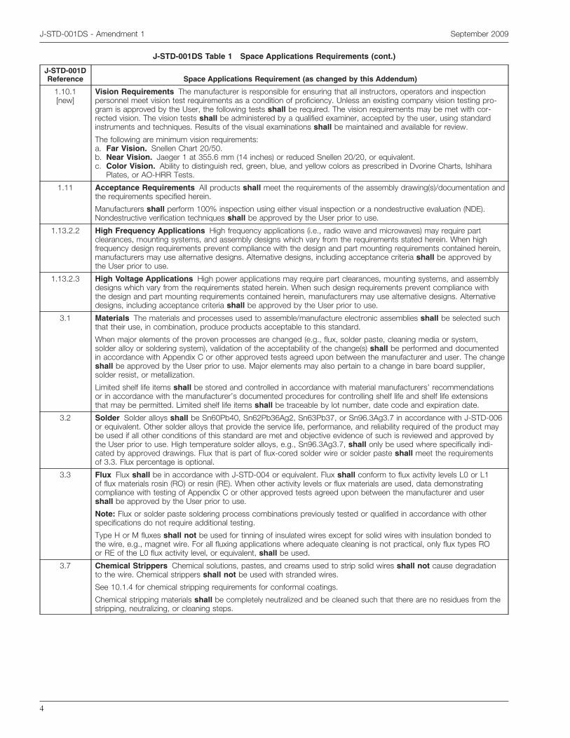
J-STD-001DS Table 1 Space Applications Requirements (cont.)
J-STD-001DReference Space Applications Requirement (as changed by this Addendum)
1.10.1[new]
Vision Requirements The manufacturer is responsible for ensuring that all instructors, operators and inspectionpersonnel meet vision test requirements as a condition of proficiency. Unless an existing company vision testing pro-gram is approved by the User, the following tests shall be required. The vision requirements may be met with cor-rected vision. The vision tests shall be administered by a qualified examiner, accepted by the user, using standardinstruments and techniques. Results of the visual examinations shall be maintained and available for review.
The following are minimum vision requirements:a. Far Vision. Snellen Chart 20/50.b. Near Vision. Jaeger 1 at 355.6 mm (14 inches) or reduced Snellen 20/20, or equivalent.c. Color Vision. Ability to distinguish red, green, blue, and yellow colors as prescribed in Dvorine Charts, Ishihara
Plates, or AO-HRR Tests.
1.11 Acceptance Requirements All products shall meet the requirements of the assembly drawing(s)/documentation andthe requirements specified herein.
Manufacturers shall perform 100% inspection using either visual inspection or a nondestructive evaluation (NDE).Nondestructive verification techniques shall be approved by the User prior to use.
1.13.2.2 High Frequency Applications High frequency applications (i.e., radio wave and microwaves) may require partclearances, mounting systems, and assembly designs which vary from the requirements stated herein. When highfrequency design requirements prevent compliance with the design and part mounting requirements contained herein,manufacturers may use alternative designs. Alternative designs, including acceptance criteria shall be approved bythe User prior to use.
1.13.2.3 High Voltage Applications High power applications may require part clearances, mounting systems, and assemblydesigns which vary from the requirements stated herein. When such design requirements prevent compliance withthe design and part mounting requirements contained herein, manufacturers may use alternative designs. Alternativedesigns, including acceptance criteria shall be approved by the User prior to use.
3.1 Materials The materials and processes used to assemble/manufacture electronic assemblies shall be selected suchthat their use, in combination, produce products acceptable to this standard.
When major elements of the proven processes are changed (e.g., flux, solder paste, cleaning media or system,solder alloy or soldering system), validation of the acceptability of the change(s) shall be performed and documentedin accordance with Appendix C or other approved tests agreed upon between the manufacturer and user. The changeshall be approved by the User prior to use. Major elements may also pertain to a change in bare board supplier,solder resist, or metallization.
Limited shelf life items shall be stored and controlled in accordance with material manufacturers’ recommendationsor in accordance with the manufacturer’s documented procedures for controlling shelf life and shelf life extensionsthat may be permitted. Limited shelf life items shall be traceable by lot number, date code and expiration date.
3.2 Solder Solder alloys shall be Sn60Pb40, Sn62Pb36Ag2, Sn63Pb37, or Sn96.3Ag3.7 in accordance with J-STD-006or equivalent. Other solder alloys that provide the service life, performance, and reliability required of the product maybe used if all other conditions of this standard are met and objective evidence of such is reviewed and approved bythe User prior to use. High temperature solder alloys, e.g., Sn96.3Ag3.7, shall only be used where specifically indi-cated by approved drawings. Flux that is part of flux-cored solder wire or solder paste shall meet the requirementsof 3.3. Flux percentage is optional.
3.3 Flux Flux shall be in accordance with J-STD-004 or equivalent. Flux shall conform to flux activity levels L0 or L1of flux materials rosin (RO) or resin (RE). When other activity levels or flux materials are used, data demonstratingcompliance with testing of Appendix C or other approved tests agreed upon between the manufacturer and usershall be approved by the User prior to use.
Note: Flux or solder paste soldering process combinations previously tested or qualified in accordance with otherspecifications do not require additional testing.
Type H or M fluxes shall not be used for tinning of insulated wires except for solid wires with insulation bonded tothe wire, e.g., magnet wire. For all fluxing applications where adequate cleaning is not practical, only flux types ROor RE of the L0 flux activity level, or equivalent, shall be used.
3.7 Chemical Strippers Chemical solutions, pastes, and creams used to strip solid wires shall not cause degradationto the wire. Chemical strippers shall not be used with stranded wires.
See 10.1.4 for chemical stripping requirements for conformal coatings.
Chemical stripping materials shall be completely neutralized and be cleaned such that there are no residues from thestripping, neutralizing, or cleaning steps.
J-STD-001DS - Amendment 1 September 2009
4
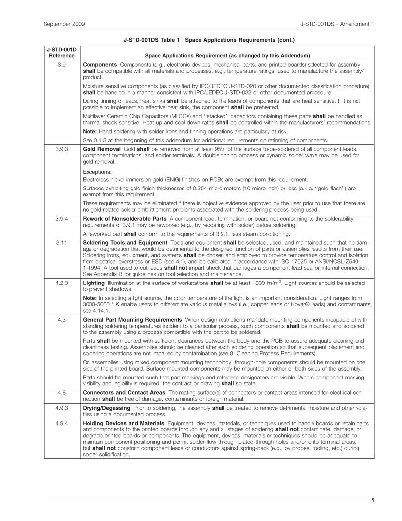
J-STD-001DS Table 1 Space Applications Requirements (cont.)
J-STD-001DReference Space Applications Requirement (as changed by this Addendum)
3.9 Components Components (e.g., electronic devices, mechanical parts, and printed boards) selected for assemblyshall be compatible with all materials and processes, e.g., temperature ratings, used to manufacture the assembly/product.
Moisture sensitive components (as classified by IPC/JEDEC J-STD-020 or other documented classification procedure)shall be handled in a manner consistent with IPC/JEDEC J-STD-033 or other documented procedure.
During tinning of leads, heat sinks shall be attached to the leads of components that are heat sensitive. If it is notpossible to implement an effective heat sink, the component shall be preheated.
Multilayer Ceramic Chip Capacitors (MLCCs) and ‘‘stacked’’ capacitors containing these parts shall be handled asthermal shock sensitive. Heat up and cool down rates shall be controlled within the manufacturers’ recommendations.
Note: Hand soldering with solder irons and tinning operations are particularly at risk.
See 0.1.5 at the beginning of this addendum for additional requirements on retinning of components.
3.9.3 Gold Removal Gold shall be removed from at least 95% of the surface to-be-soldered of all component leads,component terminations, and solder terminals. A double tinning process or dynamic solder wave may be used forgold removal.
Exceptions:Electroless nickel immersion gold (ENIG) finishes on PCBs are exempt from this requirement.
Surfaces exhibiting gold finish thicknesses of 0.254 micro-meters (10 micro-inch) or less (a.k.a. ‘‘gold-flash’’) areexempt from this requirement.
These requirements may be eliminated if there is objective evidence approved by the user prior to use that there areno gold related solder embrittlement problems associated with the soldering process being used.
3.9.4 Rework of Nonsolderable Parts A component lead, termination, or board not conforming to the solderabilityrequirements of 3.9.1 may be reworked (e.g., by recoating with solder) before soldering.
A reworked part shall conform to the requirements of 3.9.1, less steam conditioning.
3.11 Soldering Tools and Equipment Tools and equipment shall be selected, used, and maintained such that no dam-age or degradation that would be detrimental to the designed function of parts or assemblies results from their use.Soldering irons, equipment, and systems shall be chosen and employed to provide temperature control and isolationfrom electrical overstress or ESD (see 4.1), and be calibrated in accordance with ISO 17025 or ANSI/NCSL-Z540-1-1994. A tool used to cut leads shall not impart shock that damages a component lead seal or internal connection.See Appendix B for guidelines on tool selection and maintenance.
4.2.3 Lighting Illumination at the surface of workstations shall be at least 1000 lm/m2. Light sources should be selectedto prevent shadows.
Note: In selecting a light source, the color temperature of the light is an important consideration. Light ranges from3000-5000 ° K enable users to differentiate various metal alloys (i.e., copper leads or Kovar® leads) and contaminants,see 4.14.1.
4.3 General Part Mounting Requirements When design restrictions mandate mounting components incapable of with-standing soldering temperatures incident to a particular process, such components shall be mounted and solderedto the assembly using a process compatible with the part to be soldered.
Parts shall be mounted with sufficient clearances between the body and the PCB to assure adequate cleaning andcleanliness testing. Assemblies should be cleaned after each soldering operation so that subsequent placement andsoldering operations are not impaired by contamination (see 8, Cleaning Process Requirements).
On assemblies using mixed component mounting technology, through-hole components should be mounted on oneside of the printed board. Surface mounted components may be mounted on either or both sides of the assembly.
Parts should be mounted such that part markings and reference designators are visible. Where component markingvisibility and legibility is required, the contract or drawing shall so state.
4.8 Connectors and Contact Areas The mating surface(s) of connectors or contact areas intended for electrical con-nection shall be free of damage, contaminants or foreign material.
4.9.3 Drying/Degassing Prior to soldering, the assembly shall be treated to remove detrimental moisture and other vola-tiles using a documented process.
4.9.4 Holding Devices and Materials Equipment, devices, materials, or techniques used to handle boards or retain partsand components to the printed boards through any and all stages of soldering shall not contaminate, damage, ordegrade printed boards or components. The equipment, devices, materials or techniques should be adequate tomaintain component positioning and permit solder flow through plated-through holes and/or onto terminal areas,but shall not constrain component leads or conductors against spring-back (e.g., by probes, tooling, etc.) duringsolder solidification.
September 2009 J-STD-001DS - Amendment 1
5
J-STD-001DS Table 1 Space Applications Requirements (cont.)
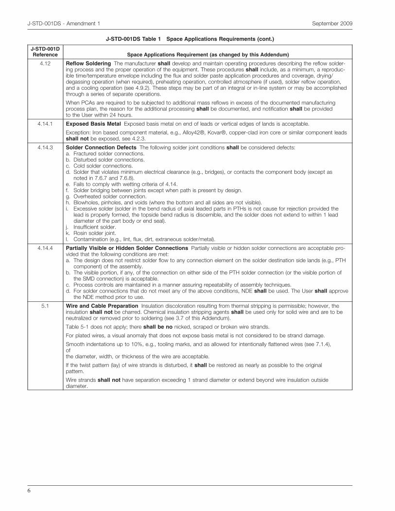
J-STD-001DReference Space Applications Requirement (as changed by this Addendum)
4.12 Reflow Soldering The manufacturer shall develop and maintain operating procedures describing the reflow solder-ing process and the proper operation of the equipment. These procedures shall include, as a minimum, a reproduc-ible time/temperature envelope including the flux and solder paste application procedures and coverage, drying/degassing operation (when required), preheating operation, controlled atmosphere (if used), solder reflow operation,and a cooling operation (see 4.9.2). These steps may be part of an integral or in-line system or may be accomplishedthrough a series of separate operations.
When PCAs are required to be subjected to additional mass reflows in excess of the documented manufacturingprocess plan, the reason for the additional processing shall be documented, and notification shall be providedto the User within 24 hours.
4.14.1 Exposed Basis Metal Exposed basis metal on end of leads or vertical edges of lands is acceptable.
Exception: Iron based component material, e.g., Alloy42®, Kovar®, copper-clad iron core or similar component leadsshall not be exposed, see 4.2.3.
4.14.3 Solder Connection Defects The following solder joint conditions shall be considered defects:a. Fractured solder connections.b. Disturbed solder connections.c. Cold solder connections.d. Solder that violates minimum electrical clearance (e.g., bridges), or contacts the component body (except as
noted in 7.6.7 and 7.6.8).e. Fails to comply with wetting criteria of 4.14.f. Solder bridging between joints except when path is present by design.g. Overheated solder connection.h. Blowholes, pinholes, and voids (where the bottom and all sides are not visible).i. Excessive solder (solder in the bend radius of axial leaded parts in PTHs is not cause for rejection provided the
lead is properly formed, the topside bend radius is discernible, and the solder does not extend to within 1 leaddiameter of the part body or end seal).
j. Insufficient solder.k. Rosin solder joint.l. Contamination (e.g., lint, flux, dirt, extraneous solder/metal).
4.14.4 Partially Visible or Hidden Solder Connections Partially visible or hidden solder connections are acceptable pro-vided that the following conditions are met:a. The design does not restrict solder flow to any connection element on the solder destination side lands (e.g., PTH
component) of the assembly.b. The visible portion, if any, of the connection on either side of the PTH solder connection (or the visible portion of
the SMD connection) is acceptable.c. Process controls are maintained in a manner assuring repeatability of assembly techniques.d. For solder connections that do not meet any of the above conditions, NDE shall be used. The User shall approve
the NDE method prior to use.
5.1 Wire and Cable Preparation Insulation discoloration resulting from thermal stripping is permissible; however, theinsulation shall not be charred. Chemical insulation stripping agents shall be used only for solid wire and are to beneutralized or removed prior to soldering (see 3.7 of this Addendum).
Table 5-1 does not apply; there shall be no nicked, scraped or broken wire strands.
For plated wires, a visual anomaly that does not expose basis metal is not considered to be strand damage.
Smooth indentations up to 10%, e.g., tooling marks, and as allowed for intentionally flattened wires (see 7.1.4),ofthe diameter, width, or thickness of the wire are acceptable.
If the twist pattern (lay) of wire strands is disturbed, it shall be restored as nearly as possible to the originalpattern.
Wire strands shall not have separation exceeding 1 strand diameter or extend beyond wire insulation outsidediameter.
J-STD-001DS - Amendment 1 September 2009
6

J-STD-001DS Table 1 Space Applications Requirements (cont.)
J-STD-001DReference Space Applications Requirement (as changed by this Addendum)
5.1.1 Tinning of Stranded Wire Solder used for tinning shall be the same alloy that will be used in subsequent solderingprocesses.
Portions of stranded wire that will be soldered shall be tinned prior to mounting when:• Wires will be formed for attachment to solder terminals.• Wires will be formed into splices (other than mesh).• Wires will be used in heat shrinkable solder device.
Stranded wires shall not be tinned when:• Wires will be used in crimp terminations.• Wires will be used in threaded fasteners.• Wires will be used in forming mesh splices.
Solder wicking shall not extend to a portion of the wire which is required to remain flexible. The solder shall wet thetinned portion of the wire and should penetrate to the inner strands of the wire. Wire strands shall be discernable aftertinning. The length of untinned strands from end of wire insulation shall not be greater than 1 wire diameter.
5.3.6 Terminal Soldering Terminals mounted in accordance with 5.3, and soldered to the printed board in unsupportedholes or noninterfacial PTHs should exhibit evidence of good wetting to both the terminal flange/shoulder and land orconductive plane. The soldered connection shall meet the requirements shown in Table 5-2.
5.5 Soldering to Terminals A solder fillet shall join the wire/lead to the terminal for 100% of the lead to terminal contactarea.
6.1.1 Lead Forming Part and component leads should be preformed to the final configuration excluding the final clinchor retention bend before assembly or installation. The lead forming process shall not damage lead seals, welds, orconnections internal to components. Leads shall not be reformed except for minor adjustments to bend angles.
Leads shall extend at least one lead diameter or thickness but not less than 0.8 mm [0.031 in] from the body orweld before the start of the bend radius (see Figure 6-1).
Note: Measurement is made from the end of the part. (The end of the part is defined to include any coating, solderseal, solder or weld bead, or any other extension.).
The lead bend radius shall be in accordance with Table 6-1.
6.1.2 Lead Deformation Limits Whether leads are formed manually or by machine or die, parts or components shall notbe mounted if the part or component lead has any nicks, scrapes or gouges. Smooth indentations up to 10%, e.g.,tooling marks, and as allowed for intentionally flattened leads (see 7.1.4), of the diameter, width, or thickness of thelead are acceptable. See 4.2.3 and 4.14.1.
Table 5-2 Terminal Soldering Requirements
A. Circumferential fillet and wetting - solder source side 360°
B. Percentage of solder source side land area covered with wetted solder 75%
Table 6-1 Lead Bend Radius
Lead Diameter Minimum Bend Radius (R)
Less than 0.8 mm [0.031 in] 1 diameter/thickness
From 0.8 to 1.2 mm [0.031 to 0.047 in] 1.5 diameters/thickness
Greater than 1.2 mm [0.047 in] 2 diameters/thickness
September 2009 J-STD-001DS - Amendment 1
7
J-STD-001DS Table 1 Space Applications Requirements (cont.)
J-STD-001DReference Space Applications Requirement (as changed by this Addendum)
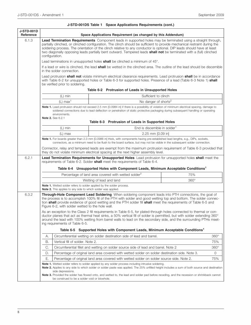
6.1.3 Lead Termination Requirements Component leads in supported holes may be terminated using a straight through,partially clinched, or clinched configuration. The clinch should be sufficient to provide mechanical restraint during thesoldering process. The orientation of the clinch relative to any conductor is optional. DIP leads should have at leasttwo diagonally opposing leads partially bent outward. Tempered leads shall not be terminated with a (full) clinchedconfiguration.
Lead terminations in unsupported holes shall be clinched a minimum of 45°.
If a lead or wire is clinched, the lead shall be wetted in the clinched area. The outline of the lead should be discerniblein the solder connection.
Lead protrusion shall not violate minimum electrical clearance requirements. Lead protrusion shall be in accordancewith Table 6-2 for unsupported holes or Table 6-3 for supported holes. Presence of a lead (Table 6-3 Note 1) shallbe verified prior to soldering.
Connector, relay and tempered leads are exempt from the maximum protrusion requirement of Table 6-3 provided thatthey do not violate minimum electrical spacing at the next higher assembly level.
6.2.1 Lead Termination Requirements for Unsupported Holes Lead protrusion for unsupported holes shall meet therequirements of Table 6-2. Solder shall meet the requirements of Table 6-4.
6.3.2 Through-Hole Component Lead Soldering When soldering component leads into PTH connections, the goal ofthe process is to accomplish 100% fill of the PTH with solder and good wetting top and bottom. The solder connec-tion shall provide evidence of good wetting and the PTH solder fill shall meet the requirements of Table 6-5 andFigure 6-2, with solder wetted to the hole wall.
As an exception to the Class 2 fill requirements in Table 6-5, for plated-through holes connected to thermal or con-ductor planes that act as thermal heat sinks, a 50% vertical fill of solder is permitted, but with solder extending 360°around the lead with 100% wetting from barrel walls to lead on the secondary side, and the surrounding PTHs meet-ing requirements of Table 6-5.
Table 6-2 Protrusion of Leads in Unsupported Holes
(L) min Sufficient to clinch
(L) max1 No danger of shorts2
Note 1. Lead protrusion should not exceed 2.5 mm [0.0984 in] if there is a possibility of violation of minimum electrical spacing, damage tosoldered connections due to lead deflection or penetration of static protective packaging during subsequent handling or operatingenvironments.
Note 2. See 6.2.1Table 6-3 Protrusion of Leads in Supported Holes
(L) min End is discernible in solder1
(L) max 2.25 mm [0.09 in]Note 1. For boards greater than 2.3 mm [0.0986 in] thick, with components having pre-established lead lengths, e.g., DIPs, sockets,
connectors, as a minimum need to be flush to the board surface, but may not be visible in the subsequent solder connection.
Table 6-4 Unsupported Holes with Component Leads, Minimum Acceptable Conditions1
Percentage of land area covered with wetted solder2 75%
Wetting of lead and land 360°Note 1. Wetted solder refers to solder applied by the solder process.Note 2. This applies to any side to which solder was applied.
Table 6-5 Supported Holes with Component Leads, Minimum Acceptable Conditions1
A. Circumferential wetting on solder destination side of lead and barrel. 360°
B. Vertical fill of solder. Note 2. 75%
C. Circumferential fillet and wetting on solder source side of lead and barrel. Note 2 360°
D. Percentage of original land area covered with wetted solder on solder destination side. Note 3. 0
E. Percentage of original land area covered with wetted solder on solder source side. Note 2. 75%Note 1. Wetted solder refers to solder applied by any solder process including intrusive soldering.Note 2. Applies to any side to which solder or solder paste was applied. The 25% unfilled height includes a sum of both source and destination
side depressions.Note 3. Provided the solder has flowed onto, and wetted to, the lead and solder pad before receding, and the recession or shrinkback cannot
be construed to be a solder void or blowhole.
J-STD-001DS - Amendment 1 September 2009
8

J-STD-001DS Table 1 Space Applications Requirements (cont.)
J-STD-001DReference Space Applications Requirement (as changed by this Addendum)
7.1 Surface Mount Device Lead Forming Leads shall be formed in such a manner that the lead-to-body seal is notdamaged or degraded (see Figures 7-1 and 7-2). When lead forming is required during the assembly process leadsshall be formed such that there is an available minimum lead length for contact to the solder pad as shown in Table7-1.
The leads of surface mounted components shall be formed to their final configuration prior to soldering.
Note: Where severe loading conditions exist such as Coefficient of Thermal Expansion (CTE) mismatches or severeoperational environments, extra consideration should be given to the minimum available contact length.
7.1.1 Surface Mount Device Lead Deformation There shall be no unintentional lead deformation beyond the limitsdefined in Paragraph 6.1.2.
7.3 Leaded Component Body Positioning The maximum clearance between the bottom of a leaded component bodyand the printed wiring surface should be 2.0 mm [0.0787 in]. Parts insulated from circuitry or over surfaces withoutexposed circuitry may be mounted flush. Uninsulated parts mounted over exposed circuitry or which are in closeproximity with other conductive materials shall be separated by suitable insulation.
7.6.3 Bottom Only Terminations Discrete chip components, leadless chip carriers, and other devices having metallizedterminations on the bottom side only (except ball grid arrays) shall meet the dimensional and solder fillet requirementsof Table 7-3 and Figure 7-3 for each product classification. The widths of the component and land are W and P,respectively, and the termination overhang describes the condition whereby the smaller extends beyond the largertermination (i.e., W or P).
Table 7-1 SMT Lead Forming Minimum Lead Length
A. Two lead width for flat leads.
B. Two lead widths for coined leads.
C. Two lead diameters for round leads.
Table 7-3 Dimensional Criteria - Bottom Only Terminations
Feature Dim. Requirement
Maximum Side Overhang A 25% (W) Note 1
End Overhang B Not permitted
Minimum End Joint Width C 75% (W) or 75% (P), whichever is less
Minimum Side Joint Length D Note 3
Maximum Fillet Height E Note 3
Minimum Fillet Height F Note 3
Solder Thickness G Note 3
Minimum End Overlap J 50% of component end termination metallization length
Termination Length L Note 2
Land Width P Note 2
Termination Width W Note 2Note 1. Does not violate minimum electrical clearance.Note 2. Unspecified parameter or variable in size, determined by design.Note 3. Wetting is evident.
1
2
3
4
J
Figure 7-3 Bottom Only Terminations1. Side overhang2. End overhang3. End joint width4. Side joint length, end overlap
September 2009 J-STD-001DS - Amendment 1
9

J-STD-001DS Table 1 Space Applications Requirements (cont.)
J-STD-001DReference Space Applications Requirement (as changed by this Addendum)
7.6.6 Castellated Terminations1. If parts with castellated terminations are chosen by design, their use shall be approved by the User. When used,
the existing J-STD-001D Class 3 requirements apply.
2. Clarification of the relationship between Features D and G: If a part has bottom metallization, the minimum sidejoint length shown as Feature D becomes Feature G, the length of the bottom metallization.
7.6.8 Round or Flattened (Coined) Leads Connections formed to round or flattened (coined ) leads shall meet thedimensional and fillet requirements of Table 7-8 and Figure 7-8 for each product classification.
Table 7-8 Dimensional Criteria - Round or Flattened (Coined) Leads
Feature Dim. Requirement
Maximum Side Overhang A 25% (W) or 0.5 mm [0.02 in], whichever is less; Note 1
Maximum Toe Overhang B Note 1
Minimum End Joint Width C 75% (W)
Minimum Side Joint Length D 100% of available lead to land interface
Maximum Heel Fillet Height E Note 4
Minimum Heel Fillet Height F (G) +(T) Note 5
Solder Thickness G Note 3
Formed Foot Length L Note 2
Minimum Side Joint Height Q (G) + 50% (T)
Thickness of Lead at Joint Side T Note 2
Flattened Lead Width or Diameterof Round Lead W Note 2
Note 1. Does not violate minimum electrical clearance.Note 2. Unspecified parameter or variable in size as determined by design.Note 3. Wetting is evident.Note 4. Solder fillet may extend through the top bend. Solder does not touch package body or end seal, except for plastic SOIC or SOT
devices. Solder should not extend under the body of surface mount components whose leads are made of Alloy 42 or similar metals.Note 5. In the case of a toe-down lead configuration, the minimum heel fillet height (F) extends at least to the mid-point of the outside lead
bend.
1 2
4
57 8
6
3
Figure 7-8 Round or Flattened (Coined) Leads1. Side overhang2. Toe overhang3. End joint width4. See Note 4, Table 7-8
5. Side joint length6. Line bisecting lower bend7. Toe down heel fillet height8. Other land configurations
J-STD-001DS - Amendment 1 September 2009
10
J-STD-001DS Table 1 Space Applications Requirements (cont.)
J-STD-001DReference Space Applications Requirement (as changed by this Addendum)
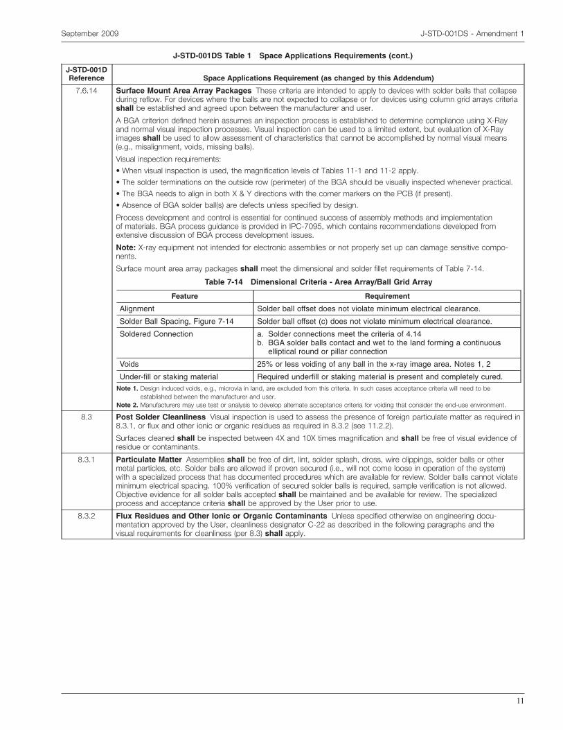
7.6.14 Surface Mount Area Array Packages These criteria are intended to apply to devices with solder balls that collapseduring reflow. For devices where the balls are not expected to collapse or for devices using column grid arrays criteriashall be established and agreed upon between the manufacturer and user.
A BGA criterion defined herein assumes an inspection process is established to determine compliance using X-Rayand normal visual inspection processes. Visual inspection can be used to a limited extent, but evaluation of X-Rayimages shall be used to allow assessment of characteristics that cannot be accomplished by normal visual means(e.g., misalignment, voids, missing balls).
Visual inspection requirements:• When visual inspection is used, the magnification levels of Tables 11-1 and 11-2 apply.• The solder terminations on the outside row (perimeter) of the BGA should be visually inspected whenever practical.• The BGA needs to align in both X & Y directions with the corner markers on the PCB (if present).• Absence of BGA solder ball(s) are defects unless specified by design.
Process development and control is essential for continued success of assembly methods and implementationof materials. BGA process guidance is provided in IPC-7095, which contains recommendations developed fromextensive discussion of BGA process development issues.
Note: X-ray equipment not intended for electronic assemblies or not properly set up can damage sensitive compo-nents.
Surface mount area array packages shall meet the dimensional and solder fillet requirements of Table 7-14.
8.3 Post Solder Cleanliness Visual inspection is used to assess the presence of foreign particulate matter as required in8.3.1, or flux and other ionic or organic residues as required in 8.3.2 (see 11.2.2).
Surfaces cleaned shall be inspected between 4X and 10X times magnification and shall be free of visual evidence ofresidue or contaminants.
8.3.1 Particulate Matter Assemblies shall be free of dirt, lint, solder splash, dross, wire clippings, solder balls or othermetal particles, etc. Solder balls are allowed if proven secured (i.e., will not come loose in operation of the system)with a specialized process that has documented procedures which are available for review. Solder balls cannot violateminimum electrical spacing. 100% verification of secured solder balls is required, sample verification is not allowed.Objective evidence for all solder balls accepted shall be maintained and be available for review. The specializedprocess and acceptance criteria shall be approved by the User prior to use.
8.3.2 Flux Residues and Other Ionic or Organic Contaminants Unless specified otherwise on engineering docu-mentation approved by the User, cleanliness designator C-22 as described in the following paragraphs and thevisual requirements for cleanliness (per 8.3) shall apply.
Table 7-14 Dimensional Criteria - Area Array/Ball Grid Array
Feature Requirement
Alignment Solder ball offset does not violate minimum electrical clearance.
Solder Ball Spacing, Figure 7-14 Solder ball offset (c) does not violate minimum electrical clearance.
Soldered Connection a. Solder connections meet the criteria of 4.14b. BGA solder balls contact and wet to the land forming a continuous
elliptical round or pillar connection
Voids 25% or less voiding of any ball in the x-ray image area. Notes 1, 2
Under-fill or staking material Required underfill or staking material is present and completely cured.Note 1. Design induced voids, e.g., microvia in land, are excluded from this criteria. In such cases acceptance criteria will need to be
established between the manufacturer and user.Note 2. Manufacturers may use test or analysis to develop alternate acceptance criteria for voiding that consider the end-use environment.
September 2009 J-STD-001DS - Amendment 1
11
J-STD-001DS Table 1 Space Applications Requirements (cont.)
J-STD-001DReference Space Applications Requirement (as changed by this Addendum)
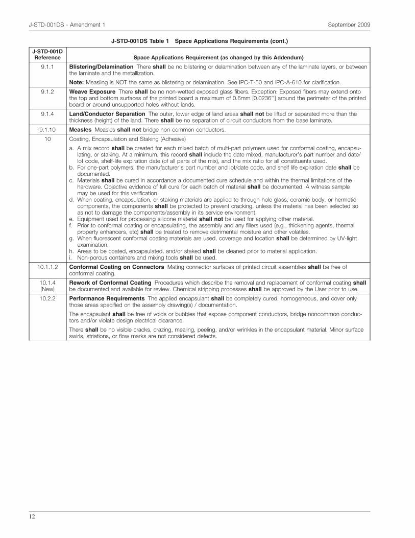
9.1.1 Blistering/Delamination There shall be no blistering or delamination between any of the laminate layers, or betweenthe laminate and the metallization.
Note: Measling is NOT the same as blistering or delamination. See IPC-T-50 and IPC-A-610 for clarification.
9.1.2 Weave Exposure There shall be no non-wetted exposed glass fibers. Exception: Exposed fibers may extend ontothe top and bottom surfaces of the printed board a maximum of 0.6mm [0.0236’’] around the perimeter of the printedboard or around unsupported holes without lands.
9.1.4 Land/Conductor Separation The outer, lower edge of land areas shall not be lifted or separated more than thethickness (height) of the land. There shall be no separation of circuit conductors from the base laminate.
9.1.10 Measles Measles shall not bridge non-common conductors.
10 Coating, Encapsulation and Staking (Adhesive)
a. A mix record shall be created for each mixed batch of multi-part polymers used for conformal coating, encapsu-lating, or staking. At a minimum, this record shall include the date mixed, manufacturer’s part number and date/lot code, shelf-life expiration date (of all parts of the mix), and the mix ratio for all constituents used.
b. For one-part polymers, the manufacturer’s part number and lot/date code, and shelf life expiration date shall bedocumented.
c. Materials shall be cured in accordance a documented cure schedule and within the thermal limitations of thehardware. Objective evidence of full cure for each batch of material shall be documented. A witness samplemay be used for this verification.
d. When coating, encapsulation, or staking materials are applied to through-hole glass, ceramic body, or hermeticcomponents, the components shall be protected to prevent cracking, unless the material has been selected soas not to damage the components/assembly in its service environment.
e. Equipment used for processing silicone material shall not be used for applying other material.f. Prior to conformal coating or encapsulating, the assembly and any fillers used (e.g., thickening agents, thermal
property enhancers, etc) shall be treated to remove detrimental moisture and other volatiles.g. When fluorescent conformal coating materials are used, coverage and location shall be determined by UV-light
examination.h. Areas to be coated, encapsulated, and/or staked shall be cleaned prior to material application.i. Non-porous containers and mixing tools shall be used.
10.1.1.2 Conformal Coating on Connectors Mating connector surfaces of printed circuit assemblies shall be free ofconformal coating.
10.1.4[New]
Rework of Conformal Coating Procedures which describe the removal and replacement of conformal coating shallbe documented and available for review. Chemical stripping processes shall be approved by the User prior to use.
10.2.2 Performance Requirements The applied encapsulant shall be completely cured, homogeneous, and cover onlythose areas specified on the assembly drawing(s) / documentation.
The encapsulant shall be free of voids or bubbles that expose component conductors, bridge noncommon conduc-tors and/or violate design electrical clearance.
There shall be no visible cracks, crazing, mealing, peeling, and/or wrinkles in the encapsulant material. Minor surfaceswirls, striations, or flow marks are not considered defects.
J-STD-001DS - Amendment 1 September 2009
12
J-STD-001DS Table 1 Space Applications Requirements (cont.)
J-STD-001DReference Space Applications Requirement (as changed by this Addendum)
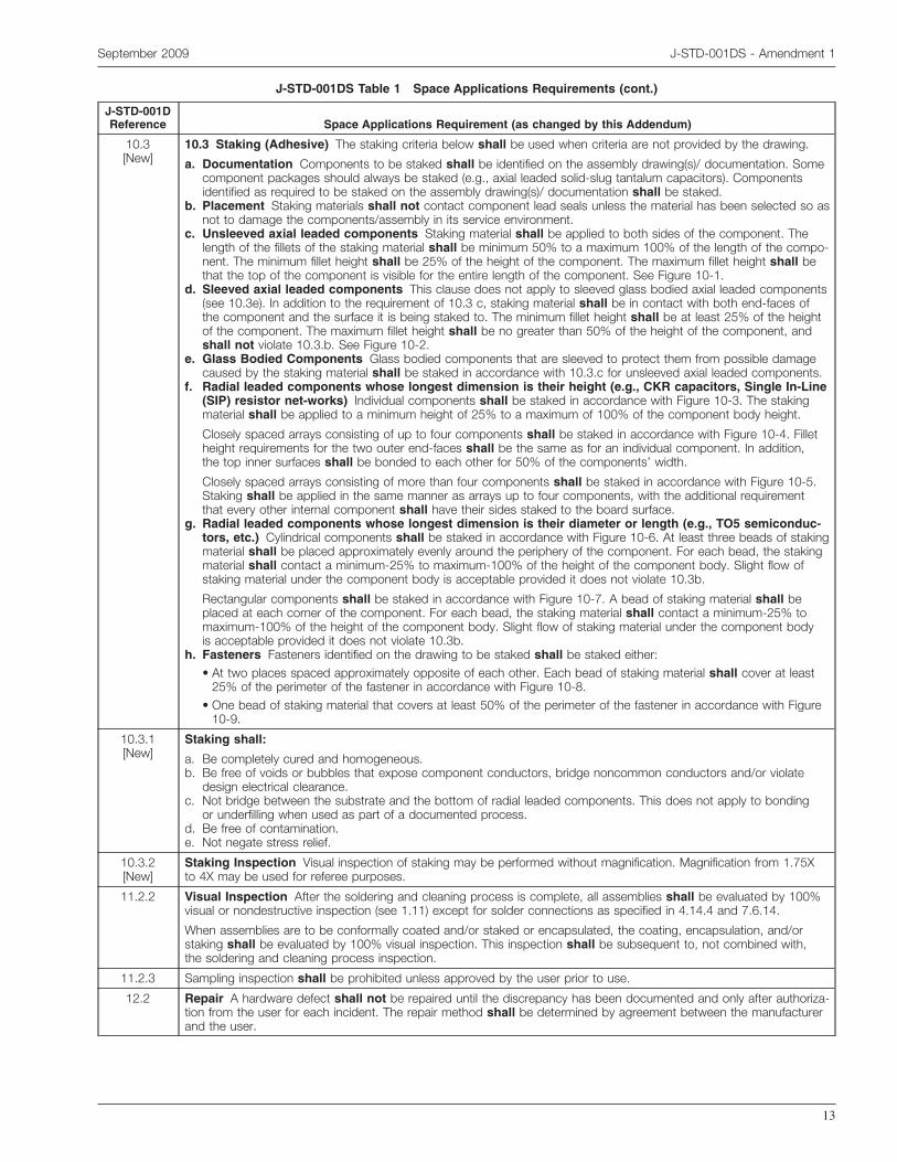
10.3[New]
10.3 Staking (Adhesive) The staking criteria below shall be used when criteria are not provided by the drawing.
a. Documentation Components to be staked shall be identified on the assembly drawing(s)/ documentation. Somecomponent packages should always be staked (e.g., axial leaded solid-slug tantalum capacitors). Componentsidentified as required to be staked on the assembly drawing(s)/ documentation shall be staked.
b. Placement Staking materials shall not contact component lead seals unless the material has been selected so asnot to damage the components/assembly in its service environment.
c. Unsleeved axial leaded components Staking material shall be applied to both sides of the component. Thelength of the fillets of the staking material shall be minimum 50% to a maximum 100% of the length of the compo-nent. The minimum fillet height shall be 25% of the height of the component. The maximum fillet height shall bethat the top of the component is visible for the entire length of the component. See Figure 10-1.
d. Sleeved axial leaded components This clause does not apply to sleeved glass bodied axial leaded components(see 10.3e). In addition to the requirement of 10.3 c, staking material shall be in contact with both end-faces ofthe component and the surface it is being staked to. The minimum fillet height shall be at least 25% of the heightof the component. The maximum fillet height shall be no greater than 50% of the height of the component, andshall not violate 10.3.b. See Figure 10-2.
e. Glass Bodied Components Glass bodied components that are sleeved to protect them from possible damagecaused by the staking material shall be staked in accordance with 10.3.c for unsleeved axial leaded components.
f. Radial leaded components whose longest dimension is their height (e.g., CKR capacitors, Single In-Line(SIP) resistor net-works) Individual components shall be staked in accordance with Figure 10-3. The stakingmaterial shall be applied to a minimum height of 25% to a maximum of 100% of the component body height.
Closely spaced arrays consisting of up to four components shall be staked in accordance with Figure 10-4. Filletheight requirements for the two outer end-faces shall be the same as for an individual component. In addition,the top inner surfaces shall be bonded to each other for 50% of the components’ width.
Closely spaced arrays consisting of more than four components shall be staked in accordance with Figure 10-5.Staking shall be applied in the same manner as arrays up to four components, with the additional requirementthat every other internal component shall have their sides staked to the board surface.
g. Radial leaded components whose longest dimension is their diameter or length (e.g., TO5 semiconduc-tors, etc.) Cylindrical components shall be staked in accordance with Figure 10-6. At least three beads of stakingmaterial shall be placed approximately evenly around the periphery of the component. For each bead, the stakingmaterial shall contact a minimum-25% to maximum-100% of the height of the component body. Slight flow ofstaking material under the component body is acceptable provided it does not violate 10.3b.
Rectangular components shall be staked in accordance with Figure 10-7. A bead of staking material shall beplaced at each corner of the component. For each bead, the staking material shall contact a minimum-25% tomaximum-100% of the height of the component body. Slight flow of staking material under the component bodyis acceptable provided it does not violate 10.3b.
h. Fasteners Fasteners identified on the drawing to be staked shall be staked either:• At two places spaced approximately opposite of each other. Each bead of staking material shall cover at least
25% of the perimeter of the fastener in accordance with Figure 10-8.• One bead of staking material that covers at least 50% of the perimeter of the fastener in accordance with Figure
10-9.
10.3.1[New]
Staking shall:
a. Be completely cured and homogeneous.b. Be free of voids or bubbles that expose component conductors, bridge noncommon conductors and/or violate
design electrical clearance.c. Not bridge between the substrate and the bottom of radial leaded components. This does not apply to bonding
or underfilling when used as part of a documented process.d. Be free of contamination.e. Not negate stress relief.
10.3.2[New]
Staking Inspection Visual inspection of staking may be performed without magnification. Magnification from 1.75Xto 4X may be used for referee purposes.
11.2.2 Visual Inspection After the soldering and cleaning process is complete, all assemblies shall be evaluated by 100%visual or nondestructive inspection (see 1.11) except for solder connections as specified in 4.14.4 and 7.6.14.
When assemblies are to be conformally coated and/or staked or encapsulated, the coating, encapsulation, and/orstaking shall be evaluated by 100% visual inspection. This inspection shall be subsequent to, not combined with,the soldering and cleaning process inspection.
11.2.3 Sampling inspection shall be prohibited unless approved by the user prior to use.
12.2 Repair A hardware defect shall not be repaired until the discrepancy has been documented and only after authoriza-tion from the user for each incident. The repair method shall be determined by agreement between the manufacturerand the user.
September 2009 J-STD-001DS - Amendment 1
13

Acceptable
• Fillet Length: 50%L, to 100%L
• Fillet Height: 25%D to 100%D. Top of component is vis-ible for its entire length.
Acceptable
• Staking is in contact with both end-faces of component(see 10.3.d).
• Fillet Height: 25%D to 50%D and does not contact leadseals or solder termination (see 10.3.b).
Acceptable
• Fillet Height 25%H to 100%H
Acceptable
• Two outside ends - fillet height: 25%H to 100%H.
• Inner surfaces - fillet is in contact with both surfaces for50% of component width.
Figure 10-1
Figure 10-2
Figure 10-3
Figure 10-4
J-STD-001DS - Amendment 1 September 2009
14

Acceptable
• Two outside ends - fillet height: 25%H to 100%H.
• Inner surfaces - fillet is in contact with both surfaces for50% of component width.
• Side of every other internal component is staked to boardsurface.
Acceptable
• At least 3 beads spaced approximately evenly aroundperiphery of component.
• Each bead fillet height 25%H to 100%H
• Slight flow underneath component, but bead(s) do notcontact lead seals (see 10.3.b).
Figure 10-5
Figure 10-6
September 2009 J-STD-001DS - Amendment 1
15

Acceptable
• At least 3 beads spaced approximately evenly aroundperiphery of component.
• Each bead fillet height 25%H to 100%H
• Slight flow underneath component, but bead(s) do notcontact lead seals or solder termination (see 10.3.b).
Acceptable
• Two beads of staking material placed approximatelyopposite of each other.
• Each bead of staking material is at least 25% of theperimeter of the fastener.
Acceptable
• One bead of staking material that covers at least 50% ofthe perimeter of the fastener.
Figure 10-7
Figure 10-8
Figure 10-9
J-STD-001DS - Amendment 1 September 2009
16

Standard Improvement Form IPC J-STD-001DSThe purpose of this form is to provide theTechnical Committee of IPC with inputfrom the industry regarding usage ofthe subject standard.
Individuals or companies are invited tosubmit comments to IPC. All commentswill be collected and dispersed to theappropriate committee(s).
If you can provide input, please completethis form and return to:
IPC3000 Lakeside Drive, Suite 309SBannockburn, IL 60015-1249Fax 847 615.7105E-mail: [email protected]
1. I recommend changes to the following:
Requirement, paragraph number
Test Method number , paragraph number
The referenced paragraph number has proven to be:
Unclear Too Rigid In Error
Other
2. Recommendations for correction:
3. Other suggestions for document improvement:
Submitted by:
Name Telephone
Company E-mail
Address
City/State/Zip Date
ASSOCIATION CONNECTINGELECTRONICS INDUSTRIES ®

ASSOCIATION CONNECTINGELECTRONICS INDUSTRIES
3000 Lakeside Drive, Suite 309S, Bannockburn, IL 60015-1249Tel. 847.615.7100 Fax 847.615.7105
www.ipc.org
®