surface-electrode architecture for ion … · 420 surface-electrode architecture for ion-trap...
TRANSCRIPT

arX
iv:q
uant
-ph/
0501
147v
2 6
Jul
200
5
Quantum Information and Computation, Vol. 5, No. 6 (2005) 419–439c© Rinton Press
SURFACE-ELECTRODE ARCHITECTURE FOR ION-TRAP
QUANTUM INFORMATION PROCESSING
J. CHIAVERINIa, R. B. BLAKESTAD, J. BRITTON, J. D. JOST, C. LANGER,D. LEIBFRIED, R. OZERI, and D. J. WINELAND
NIST, Time and Frequency Division, Ion Storage Group
325 Broadway, Boulder, CO 80305 USA
Received January 26, 2005Revised June 7, 2005
We investigate a surface-mounted electrode geometry for miniature linear radio frequencyPaul ion traps. The electrodes reside in a single plane on a substrate, and the pseudopo-tential minimum of the trap is located above the substrate at a distance on the orderof the electrodes’ lateral extent or separation. This architecture provides the possibil-ity to apply standard microfabrication principles to the construction of multiplexed iontraps, which may be of particular importance in light of recent proposals for large-scalequantum computation based on individual trapped ions.
Keywords: ion traps, quantum computation, quantum information, microfabrication,trapped ions
Communicated by : I. Cirac & R. Blatt
1 Introduction
One promising architecture for quantum information processing (QIP) is the trapping and
manipulation of individual atomic ions in radio frequency (RF) linear Paul traps [1, 2, 3,
4, 5, 6, 7]. To become a viable implementation for the execution of large-scale quantum
algorithms, this scheme requires the precise control of many ions as quantum bits (qubits).
In one possible implementation [2, 3], ion qubits are held in separate trapping regions and
moved around at will, so that selected ions may be brought into mutual proximity for the
application of quantum gates and separated again.
The proposed method [2, 3] involves holding ion qubits in “memory” zones of a trap
array (see Fig. 1). Ions to be used in a particular gate operation would be moved from
the memory zones to “processor” zones. Quantum gates could be performed on a few ions
in such a processor zone by means of entanglement of the motional modes of these ions
with their internal qubit states as, for example, in [1, 6, 8]. Single bit operations can be
performed on ions that have been moved separately into such a trapping region. For both
single- and multi-qubit operations, individual addressing of the ions through tight laser-beam
focussing would not be required [3]. With such a design, highly parallel processing is possible
(there can be many zones with interchangeable roles), and separate (shielded) regions of the
aemail: [email protected]
419
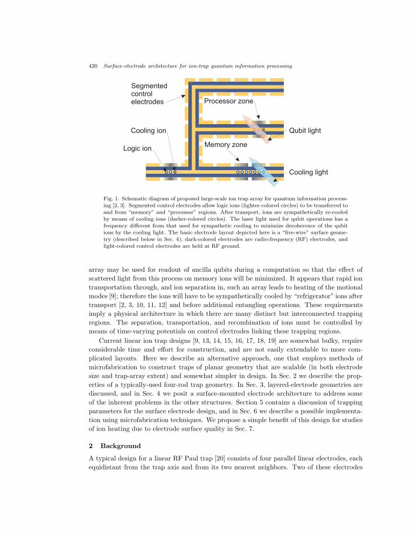
420 Surface-electrode architecture for ion-trap quantum information processing
Memory zone
Processor zone
Logic ion
Cooling ion
Segmentedcontrolelectrodes
Qubit light
Cooling light
Fig. 1. Schematic diagram of proposed large-scale ion trap array for quantum information process-ing [2, 3]. Segmented control electrodes allow logic ions (lighter-colored circles) to be transferred toand from “memory” and “processor” regions. After transport, ions are sympathetically re-cooledby means of cooling ions (darker-colored circles). The laser light used for qubit operations has afrequency different from that used for sympathetic cooling to minimize decoherence of the qubitions by the cooling light. The basic electrode layout depicted here is a “five-wire” surface geome-try (described below in Sec. 4); dark-colored electrodes are radio-frequency (RF) electrodes, andlight-colored control electrodes are held at RF ground.
array may be used for readout of ancilla qubits during a computation so that the effect of
scattered light from this process on memory ions will be minimized. It appears that rapid ion
transportation through, and ion separation in, such an array leads to heating of the motional
modes [9]; therefore the ions will have to be sympathetically cooled by “refrigerator” ions after
transport [2, 3, 10, 11, 12] and before additional entangling operations. These requirements
imply a physical architecture in which there are many distinct but interconnected trapping
regions. The separation, transportation, and recombination of ions must be controlled by
means of time-varying potentials on control electrodes linking these trapping regions.
Current linear ion trap designs [9, 13, 14, 15, 16, 17, 18, 19] are somewhat bulky, require
considerable time and effort for construction, and are not easily extendable to more com-
plicated layouts. Here we describe an alternative approach, one that employs methods of
microfabrication to construct traps of planar geometry that are scalable (in both electrode
size and trap-array extent) and somewhat simpler in design. In Sec. 2 we describe the prop-
erties of a typically-used four-rod trap geometry. In Sec. 3, layered-electrode geometries are
discussed, and in Sec. 4 we posit a surface-mounted electrode architecture to address some
of the inherent problems in the other structures. Section 5 contains a discussion of trapping
parameters for the surface electrode design, and in Sec. 6 we describe a possible implementa-
tion using microfabrication techniques. We propose a simple benefit of this design for studies
of ion heating due to electrode surface quality in Sec. 7.
2 Background
A typical design for a linear RF Paul trap [20] consists of four parallel linear electrodes, each
equidistant from the trap axis and from its two nearest neighbors. Two of these electrodes

J. Chiaverini, R. B. Blakestad, J. Britton, J. D. Jost, C. Langer, D. Leibfried, R. Ozeri, and D. J. Wineland 421
(in opposite positions about the trap axis) are driven by an RF potential, and the other two
“control” electrodes are maintained at RF ground (see Fig. 2). This geometry creates the
required quadrupolar RF field for ponderomotive confinement in the lateral directions. The
two control electrodes are segmented along their length, and static potentials can be applied
to these segments to provide longitudinal confinement.
The classical motion of a charged particle in such a trap can be determined by solving
the Mathieu equations associated with the equations of motion of the particle in the applied
potential [21, 22]. The parameters of the ion traps typically employed allow a more intuitive
solution. This is the pseudopotential approximation [23, 24], in which ions are bound through
a ponderomotive potential
U2D(r) =Q2
2mΩ2〈E2(r)〉 (1)
at position r, where Q is the particle’s charge, m is its mass, Ω is the RF drive frequency
(rad/s), and E is the magnitude of the applied electric field. For the standard quadrupole
geometry close to the trap center, this becomes
U2D(r) =Q2V 2
0
4mΩ2R4
(
x2 + y2)
(2)
if r ≡ xx + yy is the displacement from the trap axis. Here V0 is the peak amplitude of
the RF potential and R is approximately equal to the distance from the center of the trap
to the nearest electrode surface. This pseudopotential confines ions in two dimensions, and
its curvature (second spatial derivative) at the trapping location dictates their oscillation
frequency.
For typical trap parameters, one obtains the following for the motion along either of the
two radial directions (i = 1, 2), up to a relative phase:
xi(t) ≈ Xi0 cosωit[
1 +qi
2sin Ωt
]
. (3)
In this equation the xi are the usual coordinates x and y, the Xi0 are the pseudopotential
oscillation amplitudes in each direction, and the ωi are the pseudopotential oscillation fre-
quencies (less than half the RF drive frequency). The parameter qi is a normalized trap
strength
q1 = −q2 =2QV0
mΩ2R2, (4)
with a typical magnitude small compared to 1. Hence the motion in the radial directions is
composed of motion Xi0 cosωit at frequency ωi, dubbed the “secular” motion, with excursions
of smaller amplitude at the RF frequency. This superimposed motion is referred to as “mi-
cromotion,” and its amplitude is proportional to the ion’s radial secular motion displacement
from the trap center. The pseudopotential picture effectively ignores ion micromotion, which
is added as a perturbation in Eq. 3.
Figure 2 displays equal-pseudopotential contours for a linear RF Paul trap of standard,
four-rod geometry. The potential at the trapping region in the center is approximately
quadratic with a constant curvature, independent of direction in the x-y plane. Potential
local maxima (saddle points) exist at large displacements from the center at four locations

422 Surface-electrode architecture for ion-trap quantum information processing
a) b)
RF
Ions
Control
Localmaximum
Minimum(trap axis)
RF electrode
Controlelectrode
x
y
c)
RF
RF
Control
Control
Insulating layer
Fig. 2. Standard four-rod, linear RF quadrupole trap. (a) Perspective drawing of the geometry ofthis type of trap. (b) Radial pseudopotential contours (looking down the axis) of the four-rod trap.Colors from black to white indicate low to high pseudopotential, respectively. For clarity, contoursare not shown for pseudopotential values above an arbitrary maximum. (c) One implementationof the four-rod design using two conducting layers separated by an insulating layer [9].
between the trap electrodes and may provide escape pathways for energetic ions. Ions can be
readily trapped and cooled in current traps if these barriers ensure a trap depth of ∼ 1 eV or
larger.
Current and past implementations of this four-rod design have involved, for example,
macroscopic rods in a quadrupole formation [25, 26] and a quadrupole formed by the inside
edges of slots cut into pairs of alumina wafers [9] as well as other designs [13, 14, 16, 17, 18, 19].
All of these devices involve macroscopic machining of some sort. Such traps function well,
but they do not appear to offer a path toward the smaller, more complicated devices that will
be necessary for large-scale QIP with trapped ions.

J. Chiaverini, R. B. Blakestad, J. Britton, J. D. Jost, C. Langer, D. Leibfried, R. Ozeri, and D. J. Wineland 423
a) b)
RF
RF
Control
Control
RF
Control
Control
RF
Control Control
Fig. 3. Schematic diagram of modified two-layer cross to maintain a trapping potential at thecenter of the cross. Away from the cross, each of the four linear trapping regions consists of afour-rod linear trap implemented with two conducting layers as in Fig. 2c. The ions would be
trapped halfway between the two layers. (a) Top view showing diagonal bridges that connectopposite RF electrodes in both layers. Bottom layer is dark gray. Alternatively, opposing controlelectrodes can be connected. (b) Perspective view.
3 Layered Construction
A straightforward approach to incorporating microfabrication into trap construction is to use
multi-layer processing to reproduce the quadrupole geometry on a smaller scale. Although
the standard four-electrode design may be implemented with two electrode layers and an
intervening insulating layer as in [9] (see Fig. 2c), this construction is not adequate for tee
junctions and other complicated patterns. However, four-junction crosses can be made with
a slight modification to the two-layer design. Figure 3 shows the proposed modification to a
standard two-layer cross (the intersection of two linear traps, each of which is composed of two
conducting layers) such that charged particles can be trapped in the intersection region. By
connecting the RF electrodes (or alternatively the control electrodes) with diagonal bridges,
a trapping minimum can be created at the cross’s center. Variation of the potentials on
control electrode segments (not shown) allows movement of charged particles through the
cross region into any of the branches while maintaining a stable minimum at every point
along the trajectory.
As an alternative to the two-layer realization of the four-rod design, a deformation of the
quadrupole to six electrodes in a three-layer geometry allows more flexibility with trap lay-
out (see Fig. 4a) [3, 27]. This construction requires three conducting layers sandwiching two
insulating layers. A potential problem with this approach may be the difficulty of fabrication
using standard microfabrication techniques. The insulating layers must be low RF-loss ma-
terials, and ideally, they must have a thickness approximately equal to the lateral electrode
spacing. This dimension must be >∼ 10 µm to allow for optical access. For aspect ratios γ ≡width/height (Fig. 4) between 1 and 15, the depth of the trap, due to the nearby local maxima
above and below the trapping region, scales as approximately γ−2.01 for a constant trap width
(this assumes conductors rectangular in cross-section with thickness approximately 0.02 times

424 Surface-electrode architecture for ion-trap quantum information processing
the trap width). Similarly, the secular frequency obtained for a constant applied potential
at a fixed frequency with the same electrode geometry scales as approximately γ−0.93 in this
range of aspect ratios.
These scaling relations were determined numerically by means of pseudopotential calcu-
lations. This and the other simulations referred to below relied on numerical relaxation to
determine the electrostatic potential of an electrode geometry. The field was determined from
the potential, and the pseudopotential was calculated as in Eq. 1.
The scaling relations determined for the three-layer constant-width geometry suggest that
the insulating layers should be quite thick, and to facilitate fabrication, methods are required
for either deposition or deep etching of thick layers. This limits the materials and processes
that can be used. Typical materials such as silicon and gallium arsenide lead to significant RF
loss; aluminum gallium arsenide, which can be grown epitaxially on gallium arsenide, has been
suggested as an insulator [5], however. Thick layers of low-loss materials such as sapphire,
alumina, and quartz are difficult to deposit and etch. Lateral extension of the center electrodes
in the three-layer geometry beyond the upper and lower electrodes towards the center of the
trap [13] strengthens and deepens the trap, but fabrication of such a structure may require
more etch steps and hence may become more difficult.
The problems with designs of high aspect ratio (γ ≫ 1) are not as pronounced for the
standard four-electrode configuration [4, 5, 9], and small versions of this type of trap may
be built using multi-layer microfabrication. Two conducting layers and one insulating layer,
each as thin as a few micrometers, would be suitable for a trap.
4 Surface Geometry
Deformation of the standard quadrupole geometry electrodes into a plane preserves a quadrupo-
lar field for a wide range of parameters while also providing an avenue to more straightforward
fabrication. The most obvious planar deformation is to move one control electrode and one
RF electrode into the plane of the remaining two electrodes, such that the electrodes are
of alternating potential (RF, control, RF, and control), as shown in Fig. 4b. The trap axis
remains in approximately the same position, above and between the center two electrodes
(there is another trap axis symmetrically opposite this one, beneath the electrodes, but this
axis will typically reside within the substrate). This “four-wire” geometry appears promis-
ing, but making connections to the segments of both control electrodes requires multi-layer
processing or the use of vias through the substrate. Alternatively the outer RF and control
electrodes could be segmented and different control potentials applied, but this is complicated
by the practical difficulty of applying control potentials to the electrodes without affecting
application of the RF potential. An alternative is the segmentation of only the outer control
electrode for axial confinement. The asymmetry in this configuration requires adjustment
of the other (nonsegmented) control electrode to compensate for the lateral field due to the
single segmented electrode. In addition, structures such as tee junctions may be difficult to
construct with four wires in this configuration.
To alleviate these problems with the four-wire planar geometry, the four-rod quadrupole
can instead be deformed into a “five-wire” design, in which the center and outer electrodes
are maintained at RF ground, and the remaining two electrodes support an RF potential (see
Fig. 4c). In this geometry, the trap axis is above (and below) the center electrode, and the

J. Chiaverini, R. B. Blakestad, J. Britton, J. D. Jost, C. Langer, D. Leibfried, R. Ozeri, and D. J. Wineland 425
a) b)
height
width
c) d)
RF RF
Fig. 4. Radial pseudopotential contours (looking down the trap axis) for four linear RF-trapgeometries. Colors from black to white indicate low to high pseudopotential, respectively. Forclarity, contours are not shown for pseudopotential values above an arbitrary maximum. AnRF potential is applied to the gray electrodes, and the white electrodes are held at RF ground.For engineering simplicity, it would usually be more convenient to apply the control potentialsto the RF-ground electrodes. For each geometry, secular frequencies fi and trap depths umax,normalized to the values for a two-layer quadrupole with an aspect ratio (equal to the width overthe height) γ = 1 (Fig. 2c) with identical drive frequency, RF potential amplitude, and ion mass,are listed. These values are for identical distance d from the trap axis to the nearest electrodesurface and for an electrode thickness of 0.10d, and they were calculated numerically as described inthe text. (a) A three-layer geometry with γ = 1.8. For this geometry fi = 0.52 and umax = 0.078.For the simulation of this design, the electrodes were taken to extend semi-infinitely in the lateraldirections. (b) A planar geometry with trapping axis offset from the plane of the electrodes. Forthis geometry fi = 0.34 and umax = 0.017. (c) A similar trapping potential produced with asurface geometry made up of five electrodes. For this geometry fi = 0.30 and umax = 0.010.(d) A planar geometry with trapping minimum in the plane of the electrodes. For this geometryfi = 0.32 and umax = 0.051.

426 Surface-electrode architecture for ion-trap quantum information processing
a) b) c)
Fig. 5. Trap principal axes directions for three different surface trap configurations. The thirdprincipal axis is perpendicular to the page and not shown. The transverse axes directions aredepicted by two orthogonal lines at the trap axis location and are determined by static potentialsapplied between segments of the gray (RF) and white (control) electrodes. The axes directions areclose to those shown for a large range of control voltages (relative to the RF potential amplitude).
(a) Five-wire geometry, all electrodes of equal width. (b) Five-wire geometry, RF electrode widthsaltered. (c) Four-wire geometry.
two outer electrodes can be segmented for longitudinal confinement and control. There may
be advantages for ion separation if the center electrode is segmented (see below), but making
connections to the segments would require multi-layer processing or through-layer vias, a
complication we do not consider here. As the five-wire design obeys a mirror symmetry
through the plane containing the center electrode and perpendicular to the substrate plane,
tee junctions are straightforward to construct (see Fig. 1).
In a linear trap, an added static potential, as opposed to the pseudopotential, defines
the two radial major trap axes, because the pseudopotential is cylindrically symmetric near
the center of the trapping region (see Eq. 2 and Fig. 2b). In the designs discussed here, the
static potential, acting alone, leads to a maximally trapping direction and a perpendicular,
maximally anti-trapping direction in the x-y plane (perpendicular to the long direction); these
two directions define the major trap axes for the combination of the static potential and the
RF pseudopotential. By symmetry, the standard five-wire design (Fig. 4c) provides a static
potential with major trap axes perpendicular and parallel to the substrate (the third axis
in a linear trap will be along the long dimension of the wires) as in Fig. 5a. By changing
the relative lateral sizes of the electrodes, the major axes of the trap may be rotated (for
instance, if the width of one of the RF electrodes is increased by half its width, and the
width of the other RF electrode is decreased by the same amount, the principal axes rotate
by 30) as depicted in Fig. 5b. This allows Doppler-cooling laser beams whose wavevectors
are parallel to the substrate to cool the ions’ motion in both radial-axis directions [28], that
is, the ions will not be heated through recoil along any of the principal axes. This might
be necessary as beams with wavevectors nonparallel to the surface may produce significant
amounts of scattered light. The orientation of the trap principal axes in the four-wire surface
geometry is approximately ±45 from horizontal (parallel to the substrate) for a large range
of electrode potentials and thus allows laser-cooling along all three axes with a beam parallel
to the surface (see Fig. 5c).
A potential benefit of the planar electrode configuration is that the location and strength
of the trapping region may be altered by varying the electrode structure in one dimension

J. Chiaverini, R. B. Blakestad, J. Britton, J. D. Jost, C. Langer, D. Leibfried, R. Ozeri, and D. J. Wineland 427
Fig. 6. Three different options for layout of composite center control electrode in planar five-wiregeometry to allow for efficient separation of ions. A similar layout can be used in the four-wiregeometry, as well. Electrode structure appears as viewed from above the substrate. The top twoversions split the center electrode into three electrodes: the effect of the continuous electrode ineach case can be partially canceled by the shorter electrodes everywhere but in the separationregion. In the bottom version, the center electrode is split longitudinally in two continuous elec-trodes, and the separation potential can be applied to the electrode with greater extent in theseparation region. The field due to this electrode is nearly canceled outside this region by theother, relatively wider electrode.
(the lateral direction) only. Through overall scaling of the electrode size and spacing, the
distance from the trap axis to the electrodes and substrate may be controlled so that the
effects of surface proximity on ion heating [29] may be studied (see Sec. 7). This distance
can be changed continuously along the length of the electrodes, in effect creating a trapping
region for any desired surface-ion separation distance.
Another possible benefit of the surface geometry is that it may facilitate ion separa-
tion [9, 30]. Two ions or groups of ions in the same longitudinal trapping region may be
separated by raising the potential of an electrode near the center of the trapping region. As
this potential is raised, the ions’ motional frequencies necessarily drop as the external po-
tential becomes flat. The minimum motional frequency during the separation increases as
the splitting electrode’s size and the ions’ proximity to this electrode become smaller. Ac-
cording to numerical simulation, the minimum frequency ωmin is approximately proportional
to 1/L (where L is the distance from the ions to the nearest control electrode) in agreement
with [7]. We want to keep this minimum frequency as high as possible, both to minimize
kinetic excitation of the ions’ motional modes and motional heating due to stray fluctuating
charges, and to maximize the speed at which the operations can be performed [7, 9]. In the
five-wire geometry, the center electrode will be nearest to the ions (in the four-wire geometry,
the inner control electrode will be at a comparable distance from the trap axis for a similarly
sized geometry). This central electrode may be split into several segments, some with greater
extent in the longitudinal or lateral directions (see Fig. 6). Potentials applied to a subset
of these electrodes may be tuned to nearly cancel the field due to the remaining electrodes
everywhere but in a small region where the ions will be separated. The close proximity of the
electrode can lead to very efficient ion separation.
Another possible four-wire configuration that will create a quadrupole field is a pair of

428 Surface-electrode architecture for ion-trap quantum information processing
parallel RF electrodes flanked by two outer RF-ground electrodes. Here the trap axis will lie
between the two RF electrodes, as shown in Fig. 4d. This places the trap very close to the
substrate unless a slot is etched through it between these two electrodes. It also places the
RF electrodes between the trap axis and the control electrodes, limiting the effectiveness of
the control electrodes in the longitudinal direction. An alternative is the use of freestanding
wires for this design, with separate electrodes for axial confinement.
5 Strength and Depth of Surface-Electrode Geometry Trap
The trap frequencies in both surface trap designs can be made comparable to those in the
standard quadrupole of similar size. All else being equal, the radial frequencies are approx-
imately one sixth to one third (depending on exact electrode shape) of those in a standard
four-rod quadrupole of similar size (see Appendix A for a comparison to a thin-wire surface
design). However, the surface traps suffer from a much shallower trap depth. There is a local
maximum in the pseudopotential at a distance proportional to and of the same order as d
above the trap axis in both cases (see Figs. 4b, 4c, or Fig. A.1), and the depth of the trap
(defined by this maximum) is smaller by a factor of approximately 30 to 200 than the depth
of the standard quadrupole trap, depending on electrode shape. Typical trap depths for the
four-rod quadrupole design are on the order of a few electron volts (1 eV is approximately
equivalent to 12 000 K); a trap depth significantly less than this is adequate once the ion is
trapped and cooled, but the initial loading efficiency could be compromised due to the small
trap depth. Ions are typically produced by means of electron-impact ionization or photoion-
ization of a thermal neutral atomic source. Some typically trapped atomic species, such as
beryllium, must be produced from an evaporation source at a temperature of ∼ 1000 K. One
will need to depend on the low-energy tail of the Boltzmann distribution of atom kinetic
energies for trappable atoms if the trap depth is low. A possible solution is the integration of
a load/reservoir trap of a more standard design. This trap would be more efficient for loading
ions, and a large number can be obtained and held until they are needed, at which time they
can be shuttled into the surface trap for computational purposes. Also, lost ions (due to
chemical reaction or background-gas collisions) can be replaced with ions from this reservoir.
Numerical simulations suggest that a smooth crossover between the two trap geometries is
feasible.
The pseudopotential trap depth in the surface designs can be increased by adjusting the
static potential used to bring about axial confinement. The static potential due to voltages
applied to the segmented electrodes is typically trapping in the direction of one of the ra-
dial principal axes and antitrapping in the direction of the other. Calculations suggest that
variation of the principal axes angles (as mentioned above) and the magnitude of the control
voltages can deepen the trap by factors of about 2.
Although current trap designs must be reduced in size to scale to large numbers of qubits,
there may be an ultimate limit to how small any linear RF Paul trap can be made. Cal-
culations (see Appendix B) suggest that scaling beyond an ion-electrode distance of tens
of nanometers may become impossible due to reduced trap depth, even using a standard
quadrupole trap.

J. Chiaverini, R. B. Blakestad, J. Britton, J. D. Jost, C. Langer, D. Leibfried, R. Ozeri, and D. J. Wineland 429
RF electrode
Controlelectrodes
Trapping region
Micro-fabricatedfilterresistor
Filter capacitor
200 mµ
1.5 mm
Fig. 7. Micrographs of a five-wire, one-zone linear trap fabricated of gold on fused silica. The topfigure is an overview of the trap chip showing contact pads, onboard passive filter elements, leads,and trapping region. Substrate dimensions are 10 mm × 22 mm × 500 µm. The lower image is adetail of the trapping region indicated by the dotted ring in the top figure. The substrate materialappears dark-colored in the lower image.
6 Implementation
Utilizing the techniques developed for the microelectronics industry, ion traps of planar ge-
ometry can be constructed in only a few fabrication steps. The basic structure can be made
by means of patterned metal deposition onto an insulating substrate. Photolithography or
electron beam lithography can be utilized to define the electrodes. This method is similar to
that used for neutral atom optics and atom guides on chips [31, 32, 33, 34, 35, 36, 37]. An
ion trap structure fabricated in this manner is shown in Fig. 7.
Calculations suggest that a trap of this construction will be capable of trapping ions
approximately 50 µm from the chip surface. Secular frequencies will be in the 10 MHz range
for an applied RF potential of amplitude 100 V at 100 MHz. Control electrode potentials of
a few volts will lead to axial frequencies in the few megahertz range. The dissipation in the

430 Surface-electrode architecture for ion-trap quantum information processing
trap can be modeled as a resistor representing the leads in series with the trap capacitance
and its equivalent series resistance, which is proportional to the dielectric loss. In this case,
the dissipated power will be P = I2RMS(RLead + RESR) = (CΩVRMS)2(RLead + tan δ/(CΩ)),
where IRMS is the root-mean-square RF current, RLead is the total lead resistance, RESR =
tan δ/(CΩ) is the equivalent series resistance of the capacitance C between the RF and RF-
grounded electrodes, VRMS = V0/√
2, and tan δ is the loss due to the substrate. For the trap
parameters listed above, lead resistance totalling 1 Ω, a total trap capacitance of 3 pF, and
a loss tangent of 0.0004 (for fused silica), the dielectric loss is slightly less than the resistive
loss, and the RF power dissipation in the trap in Fig. 7 is 20 mW (see Appendix C for a list
of material and electrical properties for typical and suggested substrates). The values for the
lead resistance and capacitance are correct for the structure shown in Fig. 7, but will vary
with the overall size of the trap and the number of electrodes.
The control electrodes require RF grounding capacitors, and it is desirable to filter the
external control potentials with low-pass RC filters. We have typically accomplished this with
a separate board containing surface-mounted components and another set of connections be-
tween this “filter board” and the trap [9]. Typical values for the resistor and capacitor are
approximately 1 kΩ and 1 nF, respectively, leading to a high frequency roll-off of approxi-
mately 160 kHz. With these components, control electrode voltages can be changed such that
ions can be transported in segmented traps in tens of microseconds. Future traps may need
to employ filters with higher roll-off frequencies so that ions can be transported more quickly.
Since the fabrication procedure for the planar trap is relatively straightforward, passive
filter elements may be incorporated directly on the trap chip. The chip shown in Fig. 7
contains a low-pass filter on each control electrode lead consisting of a resistor and capacitor
to ground. The resistor is a long, thin meander wire of the same metal as the trap electrodes,
and the capacitor is a separate surface-mount component. Capacitors could be made during
the microfabrication, as a pair of parallel plates with silicon dioxide as an insulator. This
construction adds two thin-film depositions to the fabrication.
One concern with this design is the proximity of insulating surfaces between the electrodes
that can hold charge and perturb the trapping field in the vicinity of the ions. In the proposed
surface electrode configuration, the spaces between the electrodes will be bare insulator, and
charges on these surfaces may be problematic. To minimize the effect of charging, trenches
that undercut the metal layer may be etched into the substrate between the electrodes; if the
depth of the trenches is more than a few times the width of the space between the electrodes,
the (possibly charged) insulator’s influence on the field at the ion will be suppressed. Toward
this end, the insulator may be etched via a wet chemical etch or a reactive ion etch after
an additional lithographic masking step. An alternative is to electroplate the electrodes to a
height more than a few times the inter-electrode spacing to accomplish the same effect.
The choice of materials used in the construction of these traps is important as the elec-
trode surface can influence vibrational-mode heating of the ions (see next section), and the
substrate supporting these electrodes must have low RF loss. The planar trap fabrication, as
described above, may incorporate many different metals, as evaporation, sputtering, and elec-
troplating can employ a wide variety of materials. Gold’s relative surface cleanliness makes
it a reasonable choice, although refractory metals or other noble metals that do not support
significant surface oxides may also be investigated. Similarly, there are many choices for

J. Chiaverini, R. B. Blakestad, J. Britton, J. D. Jost, C. Langer, D. Leibfried, R. Ozeri, and D. J. Wineland 431
substrate material, as the fabrication method requires only a relatively smooth surface and
reasonable adhesion properties to metal films. Fused silica and quartz have the added ben-
efits of low RF loss and some ability to be etched. Other options include aluminum nitride,
sapphire, alumina, and diamond, although etching difficulties with the latter three materials
may imply use only in the electroplating procedure. Doped silicon may also be used as an
electrode material, and the electrodes can be defined using through-wafer reactive ion etching
(ions have been trapped in a doped silicon structure of the standard quadrupole design [38]).
There would be no insulator near the trapped ion’s position, and optical access may be pro-
vided through etched gaps between the electrodes in the planar structure. The doped silicon
electrodes can be supported by a glass substrate (away from the trapping region) attached by
means of anodic wafer bonding [39]. Gallium-arsenide and aluminum-gallium-arsenide com-
binations could also be good electrode choices [40], and in a separate design, silicon carbide
has been suggested to provide structural support for metallic electrodes [41].
The effect of a dielectric substrate on the trapping fields above the surface-mounted elec-
trodes must be considered, as many of the suggested materials have relative dielectric constant
ǫ > 10. The field in the dielectric will be modified, and at the dielectric-vacuum interface, a
component of the electric field will be discontinuous. This may lead to modification of the field
at the location of the ions. Simulations of the surface geometry with a substrate with ǫ = 1
(which is the case for all the field simulations discussed above) have been compared to similar
simulations with a substrate with ǫ = 10. For gaps between the electrodes as big as 1/4 the
width of the electrode segments, the difference in the electric field in and near the trapping
region is on the 1 % level. This difference will be smaller for the smaller relatively-sized gaps
employed in current designs, but it could be significant in the limit of thin wire-electrodes
separated by large open regions of the substrate surface.
We also note that the proximity of the electrodes to the ions possible with the surface-
electrode design suggests the possibility of performing single-qubit rotations by use of mi-
crowaves delivered to the ions via the trap structure. A subset of the planar trap wires
could make up a waveguide or cavity for long-wavelength radiation. Unlike coherent oper-
ations performed via two-photon stimulated-Raman transitions, single-bit rotations brought
about using microwaves are practically immune to the effects of spontaneous emission [2, 42].
Such manipulation of electronic hyperfine levels using near-field microwave radiation has been
proposed for ion traps [42] and neutral-atom chip-traps [43].
7 Heating Studies
Heating of a trapped ion’s motional modes can occur from thermal electronic noise in the metal
of the electrodes (or in resistive elements connected to these electrodes), fluctuating patch
potentials on the surfaces of the electrodes, and perhaps other unknown sources. Each creates
heating rates that scale as some power of the distance between the ion and the electrodes [29,
44]. The planar trap described above offers a method to study the effects of this type of
heating and to verify the scaling with distance.
Heating due to Johnson noise in the electrodes will cause fluctuations in the field at the ion,
and the heating rate due to these fluctuations is expected to scale as d−3 for d ≪ δS , where d
is the distance from ion to electrode and δS is the skin depth of the electrode metal [44]. For
d ≫ δS , the heating rate should scale as d−2 [29, 44, 45]. Heating due to fluctuating surface

432 Surface-electrode architecture for ion-trap quantum information processing
patch potentials may scale more steeply. Ref. [29] indicates a scaling of d−4 if the size of the
patches is smaller than d.
The geometry described above can easily be made smaller than most current designs, and
hence the trapped ions can be placed much closer to the electrodes than in previous traps.
The spacing and size of the planar electrodes may be changed as a function of distance along
the trap axis, therefore varying the ion-electrode distance over a wide range on one chip.
Tests of the scaling of these heating rates is very important as traps become smaller. The
requirements for sympathetic cooling and constraints on ion motion must be determined, and
these depend crucially on the heating rate.
As in other small ion traps, there is a concern with accumulated films of the to-be-trapped
material on the trap electrodes. There has been some evidence that this material can lead
to ion motional-state heating at anomalously high rates [9, 29]. In light of the attainable
proximity of ions to the electrodes in the surface geometry, this may be even more important
in this case. Large-scale designs may require separate loading and experimental zones as has
been implemented in previous designs [46].
Charging of trap or structural components due to electrons from impact ionization may
also lead to unpredictable heating or ion-trapping behavior. A separate loading zone can
alleviate this problem if the experimental zone is sufficiently far away. Alternately, photoion-
ization may be employed if suitable radiation sources are available; the usefulness of this
technique is ion-species-specific, however.
8 Remarks
We have explored the feasibility of some different linear ion-trap electrode geometries in the
context of multiplexed trapped-ion quantum information processing. Both four- or five-wire
surface geometries comprising metal deposited on an electrically insulating substrate can
maintain a trap axis above the chip and are promising for scaling ion systems toward large-
scale quantum information processing. The fabrication of such trap chips is straightforward,
and allows for rapid turnaround in design and construction as well as the inclusion of compli-
cated electrode patterns without additional fabrication effort. This design also allows for the
construction of traps much smaller than those currently in use, a necessity for faster ion-qubit
logic operations. Ion motional heating, which may ultimately limit the size and speed of these
ion trap arrays, may also be explored in designs of this type. Experiments whose goal is to
trap atomic ions in this type of electrode structure are currently underway. Planar traps of
similar design have been demonstrated recently for macroscopic charged particles [47]. We
have also suggested a modification of a two-layer design to allow crosses at the intersection
of two linear traps to facilitate two-dimensional ion-trap arrays.
After submission of this manuscript, a publication suggesting a planar Penning-trap de-
sign came to our attention [48]. In contrast to the RF Paul trap designs discussed here,
Penning traps use combined static electric and magnetic fields to trap charged particles in
three dimensions.
Acknowledgements
DJW thanks M. Prentiss (Harvard University) for the suggestion of planar electrode geome-
tries. The authors thank J. Koelemeij and S. Seidelin for helpful comments on the manuscript.
J. Chiaverini, R. B. Blakestad, J. Britton, J. D. Jost, C. Langer, D. Leibfried, R. Ozeri, and D. J. Wineland 433
This work was supported by the U.S. National Security Agency (NSA) and the Advanced Re-
search and Development Activity (ARDA). This manuscript is work of the National Institute
of Standard and Technology and is not subject to U.S. copyright.
References
1. J. I. Cirac and P. Zoller, “Quantum Computations with Cold Trapped Ions,” Phys. Rev. Lett. 74,4091–4094 (1995).
2. D. J. Wineland et al., “Experimental issues in coherent quantum-state manipulation of trappedatomic ions,” J. Res. Natl. Inst. Stand. Technol. 103 (3), 259–328 (1998).
3. D. Kielpinski, C. Monroe, and D. J. Wineland, “Architecture for a Large-Scale Ion-Trap QuantumComputer,” Nature 417, 709–711 (2002).
4. D. Leibfried, et al., “Towards quantum information with trapped ions at NIST,” J. Phys. B 36,599–612 (2003).
5. M. J. Madsen, W. K. Hensinger, D. Stick, J. A. Rabchuk, and C. Monroe, “Planar ion trapgeometry for microfabrication,” Appl. Phys. B 78, 639–651 (2004).
6. C. F. Roos et al., “Control and Measurement of Three-Qubit Entangled States,” Science 304,1478 (2004).
7. J. P. Home and A. M. Steane, “Electric octopole configurations for fast separation of trappedions,” arXiv:quant-ph/0411102 (2004).
8. D. Leibfried et al., “Experimental demonstration of a robust, high-fidelity geometric two ion-qubitphase gate,” Nature 422, 412–415 (2003).
9. M. A. Rowe, et al., “Transport of quantum states and separation of ions in a dual RF ion trap,”Quant. Inf. Comput. 2, 257–271 (2002).
10. H. Rohde et al., “Sympathetic ground-state cooling and coherent manipulation with two-ion crys-tals,” J. Opt. B Quantum Semiclassical Opt. 3, S34-S41 (2001).
11. B. B. Blinov et al., “Sympathetic Cooling of trapped Cd+ isotopes,” Phys. Rev. A 65, 040304(2002).
12. M. D. Barrett et al., “Sympathetic cooling of 9Be+ and 24Mg+ for quantum logic,” Phys. Rev. A68, 042302 (2003).
13. C. A. Schrama, E. Peik, W. W. Smith, and H. Walther, “Novel miniature ion traps,” Opt. Com-mun. 101, 32–36 (1993).
14. H. C. Nagerl, W. Bechter, J. Eschner, F. Schmidt-Kaler, and R. Blatt, “Ion strings for quantumgates,” Appl. Phys. B 66, 603–608 (1998).
15. Ralph G. DeVoe, “Elliptical ion traps and trap arrays for quantum computation,” Phys. Rev. A58, 910–914 (1998).
16. P. A. Barton et al., “Measurement of the lifetime of the 3d2D5/2 state in 40Ca+,” Phys. Rev. A
62, 032503 (2000).17. G. R. Guthohrlein, M. Keller, K. Hayasaka, W. Lange, and H. Walther, “A single ion as a
nanoscopic probe of an optical field,” Nature 414, 49–51 (2001).18. L. Hornekær, N. Kjærgaard, A. M. Thommesen, and M. Drewsen, “Structural Properties of Two-
Component Coulomb Crystals in Linear Paul Traps,” Phys. Rev. Lett. 86, 1994–1997 (2001).19. D. J. Berkeland, “Linear Paul trap for strontium ions,” Rev. Sci. Instrum. 73, 2856–2860 (2002).20. W. Paul, “Electromagnetic traps for charged and neutral particles,” Rev. Mod. Phys. 62, 531–540
(1990).21. E. Fischer, “The three dimensional stabilizing of charged particles in a quadrupole field,” Z. Phys.
156, 1–26 (1959).22. R. F. Wuerker, H. Shelton, and R. V. Langmuir, “Electrodynamic Containment of Charged Par-
ticles,” J. Appl. Phys. 30, 342–349 (1959).23. H. G. Dehmelt, “Radiofrequency spectroscopy of stored ions I: Storage,” Adv. Atom. Mol. Phys.
3, 53 (1967).

434 Surface-electrode architecture for ion-trap quantum information processing
24. P. K. Ghosh, Ion Traps (Clarendon Press, Oxford, 1995).25. J. D. Prestage, G. J. Dick, and L. Maleki, “New ion trap for frequency standard applications,” J.
Appl. Phys. 66, 1013 (1989).26. M. G. Raizen, J. M. Gilligan, J. C. Bergquist, W. M. Itano, and D. J. Wineland, “Ion crystals in
a linear Paul trap,” Phys. Rev. A 45, 6493 (1992).27. L. Deslauriers, et al., “Zero-point cooling and low heating of trapped 111Cd+ ions,” Phys. Rev. A
70, 043408 (2004).28. W. M. Itano and D. J. Wineland, “Laser cooling of ions stored in harmonic and Penning traps,”
Phys. Rev. A 25, 35–54 (1982).29. Q. A. Turchette et al., “Heating of trapped ions from the quantum ground state,” Phys. Rev. A
61, 063418 (2000).30. M. D. Barrett et al., “Deterministic quantum teleportation with atomic qubits,” Nature 429,
737–739 (2004).31. E. A. Hinds and I. G. Hughes, “Magnetic atom optics: mirrors, guides, traps, and chips for atoms,”
J. Phys. D: Appl. Phys. 32, R119–R146 (1999).32. D. C. Lau et al., “Magnetic mirrors with micron-scale periodicities for slowly moving neutral
atoms,” J. Opt. B Quantum Semiclassical Opt. 1, 371–377 (1999).33. R. Folman et al., “Controlling Cold Atoms using Nanofabricated Surfaces: Atom Chips,” Phys.
Rev. Lett. 84, 4749–4752 (2000).34. N. H. Dekker et al., “Guiding neutral atoms on a chip,” Phys. Rev. Lett. 84, 1124–1127 (2000).35. J. Reichel, W. Hansel, P. Hommelhoff, and T.W. Hansch, “Applications of integrated magnetic
microtraps,” Appl. Phys. B 72, 81–89 (2001).36. D. Muller et al., “Magnetic switch for integrated atom optics,” Phys. Rev. A 63, 041602 (2001).37. B. Lev, “Fabrication of micro-magnetic traps for cold neutral atoms,” Quant. Inf. Comput. 3,
450–464 (2003).38. J. Britton et al., unpublished.39. D. Kielpinski, Entanglement and decoherence in a trapped-ion quantum register, Ph. D. thesis,
Department of Physics, University of Colorado, Boulder (2001).40. C. Monroe, private communication.41. A. Ben-Kish and R. Folman, private communication.42. F. Mintert and C. Wunderlich, “Ion-Trap Quantum Logic Using Long-Wavelength Radiation.”
Phys. Rev. Lett. 87, 257904 (2001).43. P. Treutlein, P. Hommelhoff, T. Steinmetz, T. W. Hansch, and J. Reichel, “Coherence in Microchip
Traps,” Phys. Rev. Lett. 92, 203005 (2004).44. C. Henkel, S. Potting, and M. Wilkens, “Loss and heating of particles in small and noisy traps,”
Appl. Phys. B 69, 379–387 (1999).45. D. J. Wineland and H. G. Dehmelt, “Principles of the stored ion calorimiter,” J. Appl. Phys. 46,
919–930 (1975).46. J. Chiaverini et al., “Recent experiments in trapped-ion quantum information processing at NIST,”
Proceedings of the 2005 International Conference on Coherent and Nonlinear Optics (ICONO2005), St. Petersburg, Russia, to be published in the Proceedings of the SPIE (2005).
47. I. L. Chuang, private communication.48. S. Stahl et al., “A planar Penning trap,” Eur. Phys. J. D 32, 139–146 (2005).49. G. R. Janik, J. D. Prestage, and L. Maleki, “Simple analytic potentials for linear ion traps,” J.
Appl. Phys. 67, 6050–6055 (1990).50. R. Gomer, Field Emission and Field Ionization (Harvard University Press, Cambridge 1961).51. L. Tian and P. Zoller, “Coupled Ion-Nanomechanical Systems,” Phys. Rev. Lett. 93, 266403
(2004).

J. Chiaverini, R. B. Blakestad, J. Britton, J. D. Jost, C. Langer, D. Leibfried, R. Ozeri, and D. J. Wineland 435
a) b)
-1.5 -1 -0.5 0 0.5 1 1.5
-1.5
-1
-0.5
0
0.5
1
1.5
d
-1.5 -1 -0.5 0 0.5 1 1.5
-1.5
-1
-0.5
0
0.5
1
1.5
d
Fig. A.1. Complex plane showing the locations of positive line charges (‘•’), negative line charges(‘’), trap minima (‘ ’), and trap local maxima (‘×’). (a) Standard quadrupole geometry. (b)Four-wire surface electrode geometry.
Appendix A: Analytic comparison of standard quadrupole and four-wire surface
geometries
To compare the pseudopotential (in two dimensions) of the four-wire surface trap to that of
the standard quadrupole, complex variables can be used (here we follow the method of [49]).
In the following comparison we assume identical RF potentials applied to electrode structures
trapping particles of identical mass and charge, and we assume a uniform static axial potential.
We first calculate the pseudopotential of systems of line charges as a limiting case of the typical
rod or wire conductors and then discuss finite-size effects. In general, the results are directly
applicable to the case where the lateral electrode dimensions are much smaller than their
separation, but they give some qualitative insight for the case proposed above, in which the
spacings between electrodes can be small.
The complex potential due to a positive line charge with charge per unit length λ located
at z = x + iy = z0 is w(z) = −(λ/2πǫ0) ln(z − z0). The real part of this expression is the
electric potential. The electric-field components Ex and Ey can be determined by means
of the relation dw/dz = −Ex + iEy. The potential wq(z) for a standard quadrupole trap
would consist of positive line charges at z = ±1 and negative line charges at z = ±i (see
Fig. A.1a), which is wq(z) = ln[
(z2 + 1)/(z2 − 1)]
(here and below, we let λ/2πǫ0 = 1).
Since the pseudopotential is proportional to the square of the electric field, we calculate the
quantity
Υq(z) =
∣
∣
∣
∣
dwq
dz
∣
∣
∣
∣
2
=16|z|2
|z4 − 1|2 . (A.1)
The function Υq(z) is not in standard units but is suitable for comparisons between geometries.
The pseudopotential of the quadrupole can be seen to have a minimum at the origin, Υq(0) =

436 Surface-electrode architecture for ion-trap quantum information processing
0. This is the trap axis, where the distance d from the axis to the nearest line charge is
equal to 1. The second spatial derivative of the pseudopotential (the curvature) at this
point can be found to bed2Υq(z)
dz2 |z=0 = 32. There are four local maxima at the points
z = zm = ± 1√2√
3± i 1√
2√
3with Υq(zm) = 3
√3. The minimum and local maxima are labeled
in Fig. A.1a.
Applying the same analysis to a four-wire surface geometry for positive line charges at the
points z = −1/2 and z = 3/2 and negative line charges at the points z = −3/2 and z = 1/2
(see Fig. A.1b), we obtain the complex potential
ws(z) = ln(z − 1
2 )(z + 32 )
(z + 12 )(z − 3
2 ). (A.2)
This gives a pseudopotential function (now switching to x and y)
Υs(x, y) =64
(
16 x4 +(
3 − 4y2)2
+ 8x2(
3 + 4y2)
)
(
(1 − 2x)2
+ 4y2) (
(3 − 2x)2
+ 4y2)(
(1 + 2x)2
+ 4y2)(
(3 + 2x)2
+ 4y2) .
(A.3)
This is not particularly revealing, but differentiating, one finds two pseudopotential minima
Υs(0,±√
3/2) = 0, which define the trap axes above and below the surface, each a distance
d = 1 from the nearest line charge. The pseudopotential curvature at this point is 8/3,
which is 1/12 of the curvature in the standard quadrupole case, leading to radial secular
frequencies 12√
3≈ 0.29 times as large as in the standard quadrupole. There is a local maximum
above the trap axis at y = ym =
√3+4
√3
2 with Υs(0, ym) = 17+4
√3. This gives a trap depth
that is lower by a factor of 3(12 + 7√
3) ≈ 72 than that of the standard quadrupole trap.
To make an estimation more appropriate for finite-sized conductors, we consider cylindri-
cal, perfectly-conducting electrodes that approximate equipotentials due to the line charges
considered above. In the surface configuration, more charge must be placed on the inner two
wires relative to the outer two wires in order to obtain equipotentials of the same diame-
ter around all four wires. These equipotentials can be made the same size as those in the
four-rod geometry, and the near circularity of the equipotentials is such that the vertical and
horizontal diameters differ by only a few percent. We numerically estimate that the inner
two wires must have approximately 1.35 times the charge of the outer two for an electrode
diameter of 0.2 (0.2 times the distance between electrode centers). With this consideration,
the above analysis can be repeated, and we obtain trap axes at the locations (0,±1.18) and
local maxima at the locations (0,±1.96). The curvature at the minima leads to a secular
frequency approximately 0.16 times that in a similar four-rod trap, and the trap depth is
smaller by a factor of approximately 200.
Appendix B: Limits to miniaturization
With any miniaturizable ion trap geometry, one may ask how small the electrode structures
can be made. Here we calculate a lower-length-scale limit, neglecting motional heating effects
and ignoring the requirement of optical access for laser cooling. We assume stable trapping,

J. Chiaverini, R. B. Blakestad, J. Britton, J. D. Jost, C. Langer, D. Leibfried, R. Ozeri, and D. J. Wineland 437
and thus fix the normalized trap strength parameter qi (Eq. 4). For a particular ion species,
this leads to constraints on the applied RF potential amplitude and frequency as R gets smaller
(here we take R to be the approximate trap size). These constraints in turn restrict the trap
depth Umax, which must shrink as the trap size is reduced. The following discussion concerns
traps of the standard quadrupole geometry (Fig. 2) for singly-ionized species. Parameters for
the other trap structures mentioned above can be derived from the results of Sec. 5.
If we demand that qi remain fixed as R is reduced, then from Eq. 4,
V0
Ω2=
mqi
2QR2. (B.1)
The potential amplitude must be made to scale as V0 ∝ R to ensure that the electric field
amplitude at the surfaces of the electrodes E0 = V0/R will not grow, leading to breakdown, as
the trap electrodes get smaller (here we have assumed spherical electrode surfaces of radius R,
relevant for the truncation of electrodes or for junctions in an array). From this follows the
condition that the RF frequency must scale as Ω ∝ R−1/2.
The trap depth is equal to the value of the pseudopotential at the location of the lowest
nearby maximum; this location is displaced from the trap minimum by approximately R in
all geometries studied, and will be proportional to R in any case. Thus, from Eq. 2, the trap
depth is
Umax =βQ2V 2
0
4mΩ2R2. (B.2)
Here β is a geometrical factor dependent on exact electrode shape. From Eqs. B.1 and B.2,
we get
Umax =βqiQ
8V0 =
βqiQ
8E0R. (B.3)
The ion trap will cease to be useful when Umax ≈ hωi, that is, when there is only
one trapped state in the harmonic well. The secular frequency ωi is approximately equal
to qiΩ/2√
2, which for constant qi is
ωi =1
2
√
qiQE0
mR. (B.4)
The ratio Umax/hωi scales as R3/2 and will be given by
Umax
hωi=
β
4h
√
qiQmE0 R3/2. (B.5)
Taking values of E0 = 106 V/m and q1 = 0.21 for a beryllium ion (m = 9 u) trapped
in a four-rod quadrupole with β = 0.34 (as in the electrode size and configuration depicted
in Fig. 2), the trap will support at least one vibrational state (at a secular frequency of ap-
proximately 2.9 GHz) for R >∼ 1.7 nm. A more realistic limit might be somewhat larger:
for Umax/hωi = 100, R ≈ 37 nm, for instance. Current traps do not operate near the break-
down electric field (E0 ≈ 109 V/m [7, 50]), so smaller traps are possible with higher maximum
fields E0. Figure B.1 shows the trap depth and secular frequency for different trap sizes and
several values of E0 up to 109 V/m, where field emission is possible. Operating slightly below

438 Surface-electrode architecture for ion-trap quantum information processing
10−11
10−10
10−9
10−8
10−7
10−6
10−5
10−4
10−3
10−2
10−1
100
101
102
103
104
105
106
107
108
109
1010
R (m)
Well depth, secular frequency v. size for several fields E0=V
0/R
Dep
th (
h ω
)
E0 = 109 V/m
E0 = 108 V/m
E0 = 107 V/m
←
→
|
10−11
10−10
10−9
10−8
10−7
10−6
10−5
10−4
10−310
7
108
109
1010
1011
1012
1013
10−11
10−10
10−9
10−8
10−7
10−6
10−5
10−4
10−310
7
108
109
1010
1011
1012
1013
10−11
10−10
10−9
10−8
10−7
10−6
10−5
10−4
10−310
7
108
109
1010
1011
1012
1013
ω/2
π (H
z)
Fig. B.1. Trap depth and secular frequency as a function of trap size R for several maximum fieldvalues E0. The solid lines are depth, graphed on the left axis in units of hω, and the dashed linesare secular frequency ω/2π, graphed on the right axis. For this graph, qi = 0.21, m = 9 u, andβ = 0.34.
this field, trapping structures may shrink to R ≈ 0.2 nm before there are no trapped states.
At this point, the secular frequency would be a few hundred gigahertz, with a required drive
frequency of approximately 13.5 times larger. Traps with weaker intrinsic trapping potentials
compared to the four-rod quadrupole (such as all the other designs suggested here) will have
suitably larger minimum sizes using the criteria presented here.
A recent proposal for scaling ion traps to the submicrometer scale suggests using nanome-
chanical resonators (possibly even carbon nanotubes) as trap electrodes and trapping an ion
at a distance of R = 100 nm from these electrodes [51]. The authors do not consider trap
depth in this work, and we point out that such a trap would most likely need to be loaded
from a larger structure, as the depth may not be sufficient for initial ion capture.
Appendix C: Substrate/insulator material properties
Table C.1 lists values of pertinent properties for a selection of materials both currently used
and suggested for use as insulators or substrates in the construction of microfabricated ion
traps. These values are approximate and are only intended to give an idea of the relative
merit of particular materials.

J. Chiaverini, R. B. Blakestad, J. Britton, J. D. Jost, C. Langer, D. Leibfried, R. Ozeri, and D. J. Wineland 439
Table C.1. Substrate material properties. Values are given for readily available substrates atapproximately room temperature for frequencies in the RF range. In general, properties of thecrystalline materials vary in different directions or with different substrate orientations; valuesare approximate. Properties of semiconductors will vary greatly as a function of doping; values
are for low or intrinsic levels of doping. These values were obtained from various published andunpublished sources.
Material Thermal Electric Dielectric Dissipation Surface Dielectricconductivity resistivity constant factor roughness strength(W/(m K)) (Ω cm) (tan δ) (nm) (kV/mm)
AlN 180 1 × 10¹³ 8.5 3 × 10⁻⁴ 50 16Alumina (99.5 %) 30 1 × 10¹⁴ 9.8 1 × 10⁻⁴ 50 20BN 28 1 × 10¹³ 4.1 5 × 10⁻⁴ 50 30Diamond 2000 1 × 10¹⁴ 5.7 6 × 10⁻⁴ 50 1000Fused silica 1 1 × 10¹⁶ 3.9 4 × 10⁻⁴ 2 40GaAs 55 1 × 10⁸ 13 1 × 10⁻³ 25 40Quartz 7 1 × 10¹⁶ 4.5 2 × 10⁻⁴ 2 80Sapphire 45 1 × 10¹⁴ 11 1 × 10⁻⁴ 10 35Si 150 1 × 10⁵ 12 5 × 10⁻³ 25 30SiC 250 3 × 10⁵ 14 2 × 10⁻¹ 50 300