synthesis of input-rectifierless ac/dc converters - ideas to
TRANSCRIPT

176 IEEE TRANSACTIONS ON POWER ELECTRONICS, VOL. 19, NO. 1, JANUARY 2004
Synthesis of Input-Rectifierless AC/DC ConvertersC. P. Liu, Member, IEEE, Chi K. Tse, Senior Member, IEEE, N. K. Poon, Member, IEEE,
Bryan M. H. Pong, Senior Member, IEEE, and Y. M. Lai, Member, IEEE
Abstract—This paper discusses the basic construction proce-dure and topological possibilities of creating ac/dc converters out ofsimple dc/dc converters. It is shown that two separately controlleddc/dc converters are sufficient for producing a regulated dc outputand shaping the input current, from an ac voltage source, withoutthe need for input rectifiers. Some design constraints are discussed,emanating from the limitation of the conversion ratios that can beachieved by particular dc/dc converters. Selected topologies areverified experimentally. This kind of rectifierless converters findapplications in airborne power supplies where zero-crossing dis-tortions are significant because of the inevitable phase-lead effectof the input rectifier bridge.
Index Terms—AC/DC converter, circuit topology, control, dc/dcconverter, rectifier.
I. INTRODUCTION
AC/DC converters without input rectifiers have receivedsome attention because of their relative advantages in
eliminating power loss in rectifiers and reducing harmonicdistortions. In airborne applications where the mains frequencyis as high as several hundreds hertz, the phase-lead effect of theinput rectifier bridge in a power-factor-correction converter hasbeen found to cause significant zero-crossing distortions whichare impossible to eliminate [1]. Without input rectifiers, ac/dcconverters would be free from zero-crossing distortions.
One straightforward approach to implement a rectifierlessac/dc converter is to construct two circuits (two complete con-verters), each working for either positive or negative half cycleof the line period. This approach, however, requires rather com-plicated circuits [2], [3]. Another possibility is to put the equiva-lent rectification in the secondary side where the diodes performhigh-frequency as well as line-frequency rectification. This ap-proach usually requires four quadrant switches and complicatedtopologies. Also, the high-current low-voltage condition in thesecondary may present difficulty in raising the overall efficiency[4]. Recently, suitable converters having inherent ac/dc conver-sion capability have been studied by Ikriannikov and Cuk [5].However, such converters, known as bipolar-gain converters[5], do not seem to have a systematic origin from which gen-eral synthesis procedure can be derived.
Manuscript received January 27, 2003; revised July 15, 2003. This paper waspresented in part at the IEEE Power Electronics Specialists Conference, Van-couver, Canada, 2001. Recommended by Associate Editor C. A. Canessin.
C. P. Liu, N. K. Poon, and B. M. H. Pong are with the Department of Electricaland Electronic Engineering, University of Hong Kong, Hong Kong (e-mail:[email protected]).
C. K. Tse and Y. M. Lai are with the Department of Electronic and Infor-mation Engineering, Hong Kong Polytechnic University, Kowloon, Hong Kong(e-mail: [email protected]).
Digital Object Identifier 10.1109/TPEL.2003.820577
In this paper we consider the fundamental synthesis problemof a converter that converts an unrectified ac voltage to a dcvoltage, without using an input rectifier. Our aim is to derive thesimplest topology for ac/dc conversion, based on a combinationof dc/dc converters.
II. DERIVATION OF THE SIMPLEST AC/DC CONVERTER
We begin with a black-box specification of ac/dc conversion.Let be the output voltage, and be the input voltage.The ac/dc conversion specifies that
wherewhere .
(1)
In other words, we consider the usual conversion of a sinusoidalinput voltage having a peak of and frequency into a fixedoutput voltage . Our purpose is to derive the simplest input-rectifierless topology based on dc/dc converters that can fulfilthe above black-box requirement.
A. Basic Construction
First of all, we observe that simple dc/dc converters onlyconvert a dc voltage to another dc voltage. Thus, the use of adc/dc converter for ac/dc conversion is handicapped mainly byits input side which cannot admit negative voltage values. Theproblem can be hypothetically solved if one stacks up a suffi-ciently large dc voltage over the ac input voltage before feedinginto a dc/dc converter. This idea is illustrated in Fig. 1(a), where
denotes the stack-up voltage. Obviously, we need
(2)
Our next logical step is to create the required . Clearly weneed a second dc/dc converter which choicelessly must convertfrom the output voltage . This gives the basic configurationshown in Fig. 1(b), which is simply a series connection of twodc/dc converters. We may now construct our black-box ac/dcconverter as shown in Fig. 2.
Remarks on isolation—It should be noted that when con-structing the practical circuit, care should be taken to avoidshort-circuit paths that may affect voltage conversion. Onesimple solution is to use isolated converters, though not alwaysnecessarily, to realize either converter 1 or converter 2. More-over, if full isolation is required between and , then bothconverters should be isolated.
B. Constraints on Voltage Conversion Ratios
As shown in Fig. 2, converter 1 (labeled as DC/DC-1) must becapable of converting a variable dc voltage to a fixed dc voltage,
0885-8993/04$20.00 © 2004 IEEE

LIU et al.: SYNTHESIS OF INPUT-RECTIFIERLESS AC/DC CONVERTERS 177
Fig. 1. AC/DC conversion using (a) a dc/dc converter with a dc stack-upvoltage and (b) two dc/dc converters.
Fig. 2. Simplest input-rectifierless ac/dc converter.
whereas converter 2 (labeled as DC/DC-2) converts a fixed dcvoltage to another fixed dc voltage. Suppose the voltage conver-sion ratios of converter 1 and converter 2 are and , respec-tively. We have
(3)
(4)
Combining the above equations, the overall conversion ratio isgiven by
for (5)
The case when corresponds to zero-crossing of theinput waveform, i.e., where . In thiscase, the input to converter 1 and the output from converter 2are both equal to , giving
and for (6)
To determine the constraints on the choice of dc/dc converters,we first observe that
(7)
because . Thus, if , then converter 2 must bea step-up converter; otherwise, it can be an either step-up or
step-down converter. Also, from (3), we can derive the rangeof as
(8)
Thus, if , converter 1 must be a step-up converter;if , converter 1 must be a step-down converter;and if and , then converter 1must be able to do both step-down and step-up at different timein a line cycle. Table III summarizes the choice of convertersunder different voltage conditions.
C. Power Flow Consideration
We now consider the way in which power is processed in thebasic configuration shown in Fig. 2. First of all, assuming thatthe input current has the form
(9)
the condition for power balance gives
(10)
where is the output power. Thus, the power processed byconverter 1 (labeled as DC/DC-1), , is
(11)
and that by converter 2 (labeled as DC/DC-2), , is
(12)
Integrating over a half mains cycle, we get the power processedby converter 1 during the positive mains cycle and the negativehalf mains cycle, respectively, as
(13)and
(14)Likewise, we get the power processed by converter 2 during thepositive mains cycle and the negative half mains cycle as
(15)
Thus, we clearly see that the average power processed by con-verter 1 is and that by converter 2 is zero, over one completemains cycle. Both converters are required to be bi-directionalsince during the negative half mains cycle, power flow is es-sentially reversed. The overall effect is a circulation of power,which is equal to , between the two converters. Suchcirculation may undesirably degrade the efficiency. Hence, toreduce this circulation, we may need to design the circuit with alower , meaning that the stack-up voltage should be keptto minimum, as would be expected intuitively.

178 IEEE TRANSACTIONS ON POWER ELECTRONICS, VOL. 19, NO. 1, JANUARY 2004
Fig. 3. (a) and (b) Examples of simple input-rectifierless ac/dc converters. A flyback converter needed in (c) and (d) in lieu of buck-boost converter to reversevoltage polarity.
III. CIRCUIT IMPLEMENTATION OF SIMPLE AC/DCCONVERTERS
The implementation of an ac/dc converter based on the fore-going configuration can be proceeded by inserting appropriatedc/dc converters to the model. Fig. 3(a) shows a nonisolatedac/dc converter which is constructed with the buck-boost con-verter serving as both converters 1 and 2, and Fig. 3(b) showsanother nonisolated ac/dc converter which is constructed with abuck converter and a boost converter serving as converters 1 and2, respectively. Note that in Fig. 3(c) and (d), the flyback con-verter achieves polarity reversal, and does not provide isolationfor the entire ac/dc converter unless the other dc/dc converter isalso isolated.
IV. EXTENSION OF BASIC TOPOLOGIES
The same idea can be implemented with higher-order dc/dcconverters. For example, the Cuk converter has two possible dcoutlets which can be used as input to converter 2, as describedin Section II. Likewise, the zeta and SEPIC converters can servethe purpose. Fig. 4 shows the conceptual arrangement.
Suppose converter 1 (labeled as DC/DC-1 in Fig. 4) has anextra output voltage which can be used to feed converter 2(labeled as DC/DC-2). Let , and be the voltage ratiosdefined as
(16)
(17)
(18)
Fig. 4. Implementation of input-rectifierless ac/dc converter usinghigher-order dc/dc converters (DC/DC-1 can be Cuk, SEPIC or zeta converter).
The constraints imposed on the voltage ratios can be derived ina similar manner as in Section II. First of all, must be largerthan , i.e.,
(19)
Moreover, and are not independent. For the Cuk con-verter, for example, we have , which means
with as converter (20)
Obviously, we have , since for all time.Thus, (19) becomes
with as converter (21)
So, if , converter 2 should be a step-up converter; oth-erwise it can be either a step-up or step-down converter. As forconverter 1, we observe that
(22)

LIU et al.: SYNTHESIS OF INPUT-RECTIFIERLESS AC/DC CONVERTERS 179
Fig. 5. Outline of two possible control approaches.
Thus, if , converter 1 must be a step-up converter;if , converter 1 must be a step-down converter;and if and , then converter 1must be able to do both step-down and step-up at different timein a line cycle. If the Cuk converter is used, the duty cycle canbe controlled to satisfy these conditions.
V. CONTROL APPROACH
Suppose it is required that the input current be shaped toachieve unity power factor, in addition to a well regulated outputvoltage [6]–[8]. We may summarize the control requirements asfollows.
• To produce a tightly regulated dc output voltage.• To shape the input current to give unity power factor.• To crudely control the level of the dc stack-up voltage.
It can be shown theoretically that two separate control parame-ters are needed to achieve the above requirements [9], [10]. Inour circuit, the allowable control parameters are the duty cyclesof the two converters. Thus, in general, two control loops should
Fig. 6. Experimental converter circuit based on that of Fig. 3(d).
be designed, one for regulating the output voltage and the otherfor shaping the input current. Furthermore, since the convertersare bi-directional, feedback can be assigned arbitrarily to theconverters. Two cases are therefore possible:
i) Converter 1 shapes the input current while converter 2regulates the output voltage, as shown in Fig. 5(a).
ii) Converter 1 regulates the output voltage while converter2 shapes the input current, as shown in Fig. 5(b).
It is worth noting that the input current waveform can be arbi-trarily programmed by implementing suitable control of one ofthe converters. In the usual application of power factor correc-tion, the converter responsible for shaping the input current canprovide crude regulation for the stack-up voltage. This practicalcase will be illustrated in the experimental prototype to be dis-cussed in Section VI.
VI. EXPERIMENTAL VERIFICATION
In this section, we report experimental results of a selectedac/dc converter that has been constructed using the afore-described synthesis process. The types of dc/dc converters usedare same as the ones shown in Fig. 3(d), i.e.,
Convertor 1 : flyback convertor (turn ratio );Convertor 2 : boost covertor.
Referring to Table III, this particular choice of converter typeis suitable for the cases where and being any value.Moreover, efficiency consideration would suggest a low valuefor .
The control consists of two separate feedback loops, as dis-cussed in Section V. In particular, we employ the configurationshown in Fig. 5(a), i.e., an input current shaper applied to theflyback converter and an output regulator applied to the boostconverter. The input current shaper also regulates the stack-upvoltage . Figs. 6 and 7 show the experimental converter and theschematic control circuit.
We first report the test results for a 50 Hz line input, whichare summarized in Table I for two different choices of . Thewaveforms of the input voltage, input current, output voltageand stack-up voltage are shown in Fig. 8. It may be of interestto examine the conversion ratios of the individual convertersfor different input voltage levels, in order to verify the analyt-ical equations developed in Section II-B. Let and be theduty cycle of converter 1 and converter 2, respectively. Then,

180 IEEE TRANSACTIONS ON POWER ELECTRONICS, VOL. 19, NO. 1, JANUARY 2004
Fig. 7. Control circuit for (a) regulating � (crudely) and shaping input currentand (b) regulating U (tightly).
TABLE IEXPERIMENTAL MEASUREMENTS FOR AN INPUT-RECTIFIERLESS AC/DCCONVERTER USING A FLYBACKCONVERTER AND A BOOST CONVERTER
and , as defined previously, are and, respectively, where is the flyback trans-
former turn ratio. Table II shows the values of duty cycles and
Fig. 8. Waveforms of input voltage, input current, output voltage and stack-upvoltage for the rectifierless ac/dc converter operating at 50 Hz line frequency. (a)Test 1 conditions: stack-up voltage= 140 V; and (b) Test 2 condition: stack-upvoltage = 204 V. Trace 1: input voltage (100 V/div), Trace 2: input current (1A/div), Trace 3: output voltage (50 V/div), Trace 4: stack-up voltage � (100V/div). Note that the apparent dc offset of the input current does not actuallyexist and can be eliminated by “de-gaussing” the current probe.
TABLE IIMEASURED DUTY CYCLES AND VOLTAGE RATIOS FOR DIFFERENT INPUT
VOLTAGE LEVELS FOR AN INPUT-RECTIFIERLESS AC/DC CONVERTER USING A
FLYBACK CONVERTER AND A BOOST CONVERTER
LIU et al.: SYNTHESIS OF INPUT-RECTIFIERLESS AC/DC CONVERTERS 181
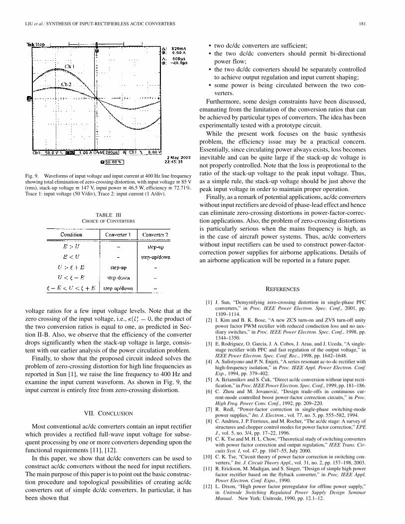
Fig. 9. Waveforms of input voltage and input current at 400 Hz line frequencyshowing total elimination of zero-crossing distortion, with input voltage= 85 V(rms), stack-up voltage = 147 V, input power= 46.5 W, efficiency= 72.71%.Trace 1: input voltage (50 V/div), Trace 2: input current (1 A/div).
TABLE IIICHOICE OF CONVERTERS
voltage ratios for a few input voltage levels. Note that at thezero crossing of the input voltage, i.e., , the product ofthe two conversion ratios is equal to one, as predicted in Sec-tion II-B. Also, we observe that the efficiency of the converterdrops significantly when the stack-up voltage is large, consis-tent with our earlier analysis of the power circulation problem.
Finally, to show that the proposed circuit indeed solves theproblem of zero-crossing distortion for high line frequencies asreported in Sun [1], we raise the line frequency to 400 Hz andexamine the input current waveform. As shown in Fig. 9, theinput current is entirely free from zero-crossing distortion.
VII. CONCLUSION
Most conventional ac/dc converters contain an input rectifierwhich provides a rectified full-wave input voltage for subse-quent processing by one or more converters depending upon thefunctional requirements [11], [12].
In this paper, we show that dc/dc converters can be used toconstruct ac/dc converters without the need for input rectifiers.The main purpose of this paper is to point out the basic construc-tion procedure and topological possibilities of creating ac/dcconverters out of simple dc/dc converters. In particular, it hasbeen shown that
• two dc/dc converters are sufficient;• the two dc/dc converters should permit bi-directional
power flow;• the two dc/dc converters should be separately controlled
to achieve output regulation and input current shaping;• some power is being circulated between the two con-
verters.Furthermore, some design constraints have been discussed,
emanating from the limitation of the conversion ratios that canbe achieved by particular types of converters. The idea has beenexperimentally tested with a prototype circuit.
While the present work focuses on the basic synthesisproblem, the efficiency issue may be a practical concern.Essentially, since circulating power always exists, loss becomesinevitable and can be quite large if the stack-up dc voltage isnot properly controlled. Note that the loss is proprotional to theratio of the stack-up voltage to the peak input voltage. Thus,as a simple rule, the stack-up voltage should be just above thepeak input voltage in order to maintain proper operation.
Finally, as a remark of potential applications, ac/dc converterswithout input rectifiers are devoid of phase-lead effect and hencecan eliminate zero-crossing distortions in power-factor-correc-tion applications. Also, the problem of zero-crossing distortionsis particularly serious when the mains frequency is high, asin the case of aircraft power systems. Thus, ac/dc converterswithout input rectifiers can be used to construct power-factor-correction power supplies for airborne applications. Details ofan airborne application will be reported in a future paper.
REFERENCES
[1] J. Sun, “Demystifying zero-crossing distortion in single-phase PFCconverters,” in Proc. IEEE Power Electron. Spec. Conf., 2001, pp.1109–1114.
[2] I. Kim and B. K. Bose, “A new ZCS turn-on and ZVS turn-off unitypower factor PWM rectifier with reduced conduction loss and no aux-iliary switches,” in Proc. IEEE Power Electron. Spec. Conf., 1998, pp.1344–1350.
[3] E. Rodriguez, O. Garcia, J. A. Cobos, J. Arau, and J. Uceda, “A single-stage rectifier with PFC and fast regulation of the output voltage,” inIEEE Power Electron. Spec. Conf. Rec., 1998, pp. 1642–1648.
[4] A. Sulistyono and P. N. Enjeti, “A series resonant ac-to-dc rectifier withhigh-frequency isolation,” in Proc. IEEE Appl. Power Electron. Conf.Exp., 1994, pp. 379–402.
[5] A. Ikriannikov and S. Cuk, “Direct ac/dc conversion without input recti-fication,” in Proc. IEEE Power Electron. Spec. Conf., 1999, pp. 181–186.
[6] C. Zhou and M. Jovanovic, “Design trade-offs in continuous cur-rent-mode controlled boost power-factor correction circuits,” in Proc.High Freq. Power Conv. Conf., 1992, pp. 209–220.
[7] R. Redl, “Power-factor correction in single-phase switching-modepower supplies,” Int. J. Electron., vol. 77, no. 5, pp. 555–582, 1994.
[8] C. Andrieu, J. P. Ferrieux, and M. Rocher, “The ac/dc stage: A survey ofstructures and chopper control modes for power factor correction,” EPEJ., vol. 5, no. 3/4, pp. 17–22, 1996.
[9] C. K. Tse and M. H. L. Chow, “Theoretical study of switching converterswith power factor correction and output regulation,” IEEE Trans. Cir-cuits Syst. I, vol. 47, pp. 1047–55, July 2000.
[10] C. K. Tse, “Circuit theory of power factor correction in switching con-verters,” Int. J. Circuit Theory Appl., vol. 31, no. 2, pp. 157–198, 2003.
[11] R. Erickson, M. Madigan, and S. Singer, “Design of simple high powerfactor rectifier based on the flyback converter,” in Proc. IEEE Appl.Power Electron. Conf. Expo., 1990.
[12] L. Dixon, “High power factor preregulator for offline power supply,”in Unitrode Switching Regulated Power Supply Design SeminarManual. New York: Unitrode, 1990, pp. 12.1–12.

182 IEEE TRANSACTIONS ON POWER ELECTRONICS, VOL. 19, NO. 1, JANUARY 2004
C. P. Liu (M’99) was born in Hong Kong in 1970. Hereceived the B.S. degree in electrical and electronicengineering from the University of Hong Kong, in1993.
From 1993 to 1999, he held several industrialpositions in switching power supply design. Since1999, he has been with the Power ElectronicsLaboratory, University of Hong Kong, where he isa Principal Engineer. His research interest includesswitching converter topologies, synchronous recti-fiers, soft switching, and EMI modeling.
Chi K. Tse (M’90–SM’97) received the B.Eng.degree (with first class honors) in electrical engi-neering and the Ph.D. degree from the Universityof Melbourne, Australia, in 1987 and 1991, respec-tively.
He is a Professor with Hong Kong PolytechnicUniversity, and his research interests includechaotic dynamics and power electronics. He is theauthor of Linear Circuit Analysis (London, U.K.:Addison-Wesley 1998) and Complex Behavior ofSwitching Power Converters (Boca Raton, FL: CRC
Press, 2003), co-author of Chaos-Based Digital Communication Systems(Heidelberg, Germany: Springer-Verlag, 2003) and co-holder of a U.S. patent.Since 2002, he has been an Advisory Professor with the Southwest ChinaNormal University, Chongqing, China.
Dr. Tse received the L.R. East Prize from the Institution of Engineers, Aus-tralia, in 1987, the IEEE TRANSACTIONS ON POWER ELECTRONICS Prize PaperAward, in 2001, the President’s Award for Achievement in Research, and theFaculty’s Best Researcher Award. He was an Associate Editor for the IEEETRANSACTIONS ON CIRCUITS AND SYSTEMS PART I—FUNDAMENTAL THEORY
AND APPLICATIONS, from 1999 to 2001, and, since 1999, has been an AssociateEditor for the IEEE TRANSACTIONS ON POWER ELECTRONICS.
N. K. Poon (M’95) received the B.Eng. degree (withhonors) in electronic engineering from the City Uni-versity of Hong Kong, in 1995, and the Ph.D. degreefrom Hong Kong Polytechnic University, in 2003.
After graduation, he worked with Artesyn Tech-nologies (Asia Pacific) Limited for three and a halfyears before joining the Power Electronics Labora-tory, University of Hong Kong. His current interestincludes soft switching techniques, EMI modeling,PFC topologies, synchronous rectification, convertermodeling, PWM inverters, and fast transient regula-
tors.
Bryan M. H. Pong (M’84–SM’96) was born inHong Kong. He received the B.Sc. degree in elec-tronic and electrical engineering from the Universityof Birmingham, U.K., in 1983 and the Ph.D. degreein power electronics from Cambridge University,U.K., in 1987.
After graduation, he became a Senior Design En-gineer and then a Chief Design Engineer at NationalSemiconductor Hong Kong, where he was involvedin electronic product design. Afterwards he joinedASTEC International, Hong Kong, first as a Principal
Engineer and then a Division Engineering Manager. He is now an Associate Pro-fessor with the University of Hong Kong, where he is in charge of the PowerElectronics Laboratory and leads a team to carry out research in switching powersupplies. His research interests include synchronous rectification, EMI issues,power factor correction, magnetic component design and soft switching. Heco-holds a number of U.S. patents.
Y. M. Lai (M’92) received the B.Eng. (with honors)degree in electrical engineering from the Universityof Western Australia, Perth, Australia, in 1983, theM.Eng.Sc. degree in electrical engineering from Uni-versity of Sydney, Sydney, Australia, in 1986, and thePh.D. degree from Brunel University, U.K., in 1997.
He is an Assistant Professor with Hong Kong Poly-technic University, Hong Kong, and his research in-terests include computer-aided design of power elec-tronics and nonlinear dynamics. Prior to joining theUniversity, he held technical positions with National
Semiconductor, Derek Philips Associates, and Siliconix Hong Kong Limited.
