synthesis of medium voltage dc-to-dc converters from low-voltage
TRANSCRIPT

IEEE TRANSACTIONS ON POWER ELECTRONICS, VOL. 22, NO. 5, SEPTEMBER 2007 1619
Synthesis of Medium Voltage dc-to-dcConverters From Low-Voltage, High-Frequency
PWM Switching ConvertersVatché Vorpérian
Abstract—Low-voltage dc-to-dc power conversion is a very ma-ture industry which uses high-frequency pulsewidth modulation(PWM) switching techniques. The passive and active componentsneeded to build low-voltage dc-to-dc converters are highly avail-able, affordable and constantly improving. In this paper, a verysimple and systematic method of using a large number of low-voltage, high-frequency PWM converters to synthesize highly re-dundant, medium voltage (4–40 kV) dc-to-dc converters is pre-sented. Theoretical and practical considerations are discussed innecessary detail and test results of an actual 10-kW, 10 kV-to-400V, converter built from 48 low-voltage forward converters are pre-sented. Real-time and average reduced circuit models are derivedto predict the dynamical behavior of the converter and to designthe feedback control loop.
Index Terms—Dc circuit breaker, feedback control, high-fre-quency, medium voltage, Neptune power, PWM conversion,reduced average model, redundancy, stacking, reduced real-timemodel.
I. INTRODUCTION
THERE has been a growing interest, in recent years, in thetransmission of power up to several thousand kilometers
to the bottom of the ocean floor for sub-sea cabled observatoriesusing medium voltages of the order of 10 kV as reported in[1]–[3]. For terrestrial applications, a similar interest exists forgeneral electric propulsion such as trains and industrial drives[4]. The technology needed to develop the 10 kV-to-400 Vdc-to-dc converter for the cabled underwater observatories wasdeveloped at the Jet Propulsion Laboratory (JPL) over a periodof three years and reported in [7] and [8]. The commercial-ization of this converter is currently underway at Alcatel [9].This paper discusses the synthesis, modeling, and analysis ofmedium voltage (MV) dc-to-dc converters using a large numberof high-frequency, low-voltage PWM converters. The conceptsand techniques presented go considerably beyond the generalintuitive idea of stacking converters which has been known fora long time but never successfully implemented in applicationsapproaching medium input voltages. Issues related to cascadingconverters are also addressed in [5] and [6].
Manuscript received August 15, 2006; revised December 15, 2006. This workwas supported by the University of Washington through funding from the Na-tional Science Foundation Ocean Technology and Interdisciplinary Coordina-tion Program: Development of a Power System for Cabled Ocean Observato-ries Grant OCE 0116750 and the Monterey Accelerated Research System GrantOCE 022650. Recommended for publication by Associate Editor J. Sun.
The author is with the Jet Propulsion Laboratory, California Institute of Tech-nology, Pasadena, CA 91011 USA (e-mail: [email protected])..
Digital Object Identifier 10.1109/TPEL.2007.904170
Fig. 1. Block diagram of an isolated LV converter in which the turns ratio ofthe isolation transformer is unity.
Among the key advantages offered by the method of syn-thesis presented in this paper are: a) inherent high redundancy;b) simplicity of design; c) modularity; and d) availability ofcomponents and materials. Another possible advantage, whichis not discussed in this paper, is that these converters naturallyact as dc circuit breakers if implemented in a dc distributionsystem because during a fault (short circuit, over-current, orover-voltage) the PWM drive signal to all the MOSFETs to allthe converter stages can be made to vanish instantly thereby in-terrupting the power flow through the MV converter. Hence, theMV converters described in this work perform the functions ofvoltage conversion and circuit breaking simultaneously whichare among the essential elements of a power distribution system.
II. SYNTHESIS OF MEDIUM-VOLTAGE DC-TO-DC CONVERTERS
FROM LOW-VOLTAGE CONVERTERS
A medium voltage (MV) converter is synthesized essentiallyby stacking a large number of isolated low-voltage (LV) con-verters, shown here in Fig. 1, in which the isolation transformerhas a 1:1 turns ratio and is capable of withstanding the rateddc MV voltage. The choice of the LV converter topology andthe method of stacking depend on the conversion ratio require-ment of the MV converter. For example, for a large step-downratio, the LV converter of choice would be a buck-derived iso-lated converter (full-bridge, half-bridge, two-switch forward)whose primary sides are stacked in series and secondary sidesare stacked in series and parallel as shown in Fig. 2.
A convention for numbering the primary and secondary sidesof an LV converter stage inside an MV converter is useful forformulating the different stacking configurations used for syn-thesizing a step-down, step-up, or step-up-down MV converter.An example of this convention is shown for the MV-to-LV con-verter in Fig. 2 where the usual row-column notation for a matrixis adopted. We shall refer to a column as a stack in this paper.Hence, a primary side which falls in the th stack and th rowis denoted by while a secondary side which falls in the thstack and th row is denoted by . For example, if is thetotal number of LV converter stages all of whose primary sidesare connected in series in a single stack as in Fig. 2, then
0885-8993/$25.00 © 2007 IEEE

1620 IEEE TRANSACTIONS ON POWER ELECTRONICS, VOL. 22, NO. 5, SEPTEMBER 2007
Fig. 2. An example of an MV converter designed for large step down(MV-to-LV) in which all the primary sides of the LV converters are connectedin series while the secondary sides are connected in series and parallel.
and . Also in Fig. 2, we see that on the secondaryside, stacks are connected in parallel , with
secondaries in each stack connected in series .Since the total number of LV converter stages is , it followsthat .
There are four important aspects of the synthesis of MVconverter just described. First, the large number of the LVconverters and the manner in which they are stacked allowthe designer to achieve the required conversion ratio withoutrelying on the turns ratio of the isolation transformer. Hence,the isolation transformer can always be designed with unityturns ratio resulting in simple construction and minimumleakage inductance. The simple construction of the isolationtransformer in turn simplifies the design against the dc break-down voltage between primary and secondary. Second, all theconstituent LV converter stages are driven with the same dutycycle. Third, synchronous rectification is used to eliminate thediscontinuous conduction mode. Fourth, in each LV converterstage, the large output or the input filter capacitor is replacedwith a much smaller capacitor and a local damping networkwhich suppresses the high frequency resonance formed bythe filter inductance and the small capacitance. A single largecapacitor is then used on the output or the input to absorb theswitching current ripple as will be explained in the followingsections.
There are four methods of stacking LV converters to synthe-size MV converters with different conversion ratio characteris-tics. The following notation is introduced in this paper to repre-sent a stacking configuration:
(1)
in which
(2)
If is the total number of LV converter stages, then we have
(3)
(4)
(5)
Fig. 3. Example of interlocked or irreducible stacking.
The four methods of stacking are as follows.1) Simple stacking: In this method of stacking, at least one
side consists of a single stack in which all the primary orsecondary sides are connected in series. The three casesfor voltage conversion can be realized by the followingstacking configurations:
(6a-c)
The most suitable topology of the LV converter stage foreach of the three cases above will be discussed in the nextthree sections.
2) Series-reducible stacking: Although there is no apparentadvantage, it is possible to stack in series several of anyof the MV converter configurations in (6), each completewith its own regulated output voltage. Series reductionor decomposition of this kind of stacking can be mathe-matically represented by the summation symbol. For ex-ample, a series reducible MV-to-LV converter, composedof simple-stacked MV-to-LV converters as in (6a), canbe formally expanded as:
(7)
3) Parallel-reducible stacking: When the power level be-comes significantly high, it may be desirable to parallelseveral of any of the simple-stacked MV converter con-figurations in (6). In this case, a single voltage feedbackis used to regulate the output voltage but the duty cycleof each MV converter is regulated independently using acurrent feedback loop from each MV converter. Parallelreduction or decomposition can be represented math-ematically using the product symbol. For example, aparallel reducible MV-to-LV converter composed ofsimple-stacked MV-to-LV converters as in (6a), can beformally expanded as
(8)
4) Irreducible or interlocking stacking: This type of stackingcannot be expanded as in (7) or (8) in terms of simple-stacked converters. An example is shown in Fig. 3 for a
stacking configuration. An important fea-ture of this stacking method is that it has the high power ca-pability of parallel-reducible stacking but does not require

VORPÉRIAN: SYNTHESIS OF MEDIUM VOLTAGE DC-TO-DC CONVERTERS FROM LOW-VOLTAGE, HIGH-FREQUENCY PWM SWITCHING CONVERTERS 1621
Fig. 4. Two-switch forward converter with an input filter in which the output filter capacitor is replaced with a small capacitor and a damping network. Theswitching frequency is 50 kHz. The values of the components shown are for the subconverter used in building the �10 kV to 400 V converter.
multiple current feedback loops to ensure current sharingamong all the converters. The current is shared among allthe converters naturally as a result of either the primarysides or the secondary sides being interlocked. For ex-ample, in Fig. 3, since all the converters are driven withthe same duty cycle and the current on the primary side ofthe first stack [(1,1) through (3,1)] is the same, it followsthat the current in the first stack [(1,1) and (2,1)] on the sec-ondary side and the secondary side (2,2) are also the same.But, since (2,2) and (1,2) are in series, their currents arethe same. This forces the current in the second stack on theprimary side [(1,2) through (3,2)] to be the same as the cur-rent in the first stack in the primary, which in turn forcesthe current in the third stack on the secondary side [(1,1)and (2,1)] to be the same as the first two.
III. SYNTHESIS OF MV-TO-LV STEP-DOWN
DC-TO-DC CONVERTERS
An MV-to-LV step down converter is synthesized naturallyby connecting the primary sides of a large number of LV con-verters in series and the secondary sides in a series and parallelconfiguration. As an illustrative example, we will determine thenumber of converters and their topology needed to synthesize anMV-to-LV converter which will deliver 10 kW at 400 V from a6 kV-to-12 kV input voltage source.
Since this is a step-down application, we shall consider usingthe two-switch forward converter, shown in Fig. 4, in which theoutput filter capacitor has been removed and replaced with asmall capacitor and a parallel damping branch whose elementvalues are given by
(9)
(10)
The voltage conversion ratio of this converter stage is
(11)
To determine the number of the LV converter stages needed,we shall allow the input of each stage not to exceed about 200to 300 V. After some basic considerations, one can verify thatforty-eight LV converter stages can be used by connecting themaccording to the following stacking configuration:
(12)
The range of the duty cycle is acceptable to the forward con-verter and is given by
(13)
Each LV stage puts out at 50 V and hasa maximum input voltage of V. Each stackon the secondary side puts out W at
V. At the 400-V output, a single 100 F is usedto filter the inductive current from all six stacks to provide asmooth output voltage with 250 mV peak-to-peak ripple voltagewhen the converter is operating at a switching frequency of 50kHz. The voltage conversion ratio of this MV-to-LV converteris given by
(14)
The two-stage input filter in Fig. 4 is damped against the nega-tive impedance loading of the converter stage. A two-stage filteris not necessary and in many cases a single stage filter isadequate. The worse case negative impedance loading occurs atminimum input voltage and maximum load which can be ex-pressed as
(15)
A simple rule for damping the input filter for unconditional sta-bility is given by
(16)
Generally, a in the range 1.2 to 2 is acceptable. One can alsofine tune the damping elements using a few CAD iterations. Fora more in-depth analysis, the reader is referred to the classicwork of Middlebrook in [13].
Some steady-state quantities of this converter example arecomputed next. The maximum peak-to-peak ripple current inthe output inductor occurs at the highest input voltageand is given by
(17)

1622 IEEE TRANSACTIONS ON POWER ELECTRONICS, VOL. 22, NO. 5, SEPTEMBER 2007
The maximum peak-to-peak output ripple voltage is given by
(18)
where we have used the fact that the ripple current flowing intothe output capacitor is the sum of the ripple current out the sixoutput stacks .
The input ripple current of a single-stage input filter isgiven by
(19)
where
(20)
For the two-stage filter, the input ripple current is given by
(21)
IV. SYNTHESIS OF LV-TO-MV STEP-UP DC-TO-DC
CONVERTERS
An LV-to-MV step-up converter is synthesized by connectingthe secondary sides of a large number of LV converters in se-ries and the primary sides in series and parallel according tothe stacking configuration in (6b). As an illustrative example,we will determine the number of converters and their topologyneeded to synthesize an LV-to-MV converter which delivers 10kV at 10 kW from a 200-to-400 V input voltage source.
Since this is a step-up application, the isolated boost convertertopology shown in Fig. 5(a) is used whose voltage conversionratio is given by
(22)
The duty cycle in (22) is defined in Fig. 5(b). Because thetransformer is center-tapped, the drain-to-source voltage of theMOSFETs during the off-time is twice the output voltage. Ifan isolation transformer without a center-tap is desired, then thevariation shown in Fig. 6 is used whose voltage conversion ratiois given by
(23)
in which the duty ratio is defined as before in Fig. 5(b). Thereason for the appearance of the factor 4 in (23) is because ofthe frequency doubling action of the split inductors on the inputside and the voltage doubling configuration at the output. The
Fig. 5. (a) Isolated boost converter with a center-tapped transformer. On theinput, a small capacitor with a damping network is used. (b) Gate-drive wave-forms and definition of duty cycle.
drain-to-source voltage of the switches on the primary side forthis topology is only half the output voltage while that of theoutput MOSFETs is equal to the output voltage. The smallestconversion ratio for this converter is 4.
Since the input voltage is fairly low, only a few converters areneeded in a stack on the primary side to divide the input voltage.On the output side, since the voltage is high, all the convertersare connected in series. According to the stacking configurationin (6b) the conversion ratio of the LV-to-MV converter is givenby
(24)
Hence, the desired LV-to-MV converter can now be built bystacking 48 of the converter Fig. 5(a) as follows:
(25)
Each converter in this configuration delivers 208 W at anoutput voltage of 208 V and operates from an input voltage of50-to-100 V. When 48 of the converters in Fig. 6 are used, thenthe stacking configuration becomes
(26)
Each converter in this configuration delivers 208 W at an outputvoltage of 208 V and operates from an input voltage of 25-to-50V.
To meet EMI requirements, a damped filter is addedat the input of the boost converter in order to attenuate theswitching current in the input inductor to an acceptable level. InFigs. 5(a) and 6, we see that the inputs of these boost convertersare stripped of this additional filter and instead a small acapacitor, , with a damping network, is used. A
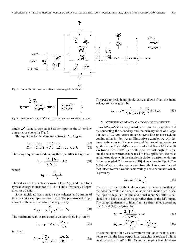
VORPÉRIAN: SYNTHESIS OF MEDIUM VOLTAGE DC-TO-DC CONVERTERS FROM LOW-VOLTAGE, HIGH-FREQUENCY PWM SWITCHING CONVERTERS 1623
Fig. 6. Isolated boost converter without a center-tapped transformer.
Fig. 7. Addition of a single LC filter at the input of an LV-to-MV converter.
single stage is then added at the input of the LV-to-MVconverter as shown in Fig. 7.
The equations for the damping network are
(27)
(28)
The design equations for damping the input filter in Fig. 7 are
(29)
where
The values of the snubbers shown in Figs. 5(a) and 6 are for atypical leakage inductance of 3–5 H and a frequency of oper-ation of 50 kHz.
Some additional basic steady state voltages and currents ofthis converter example are given next. The peak-to-peak ripplecurrent in the input inductor, , is given by
(30)
The maximum peak-to-peak output voltage ripple is given by
(31)
in which
(32)
The peak-to-peak input ripple current drawn from the inputvoltage source is given by
(33)
V. SYNTHESIS OF MV-TO-MV DC-TO-DC CONVERTERS
An MV-to-MV step-up-and-down converter is synthesizedby connecting the secondary and the primary sides of a largenumber of LV converters in series according to the stackingconfiguration in (6c). As an illustrative example, we will de-termine the number of converters and their topology needed tosynthesize an MV-to-MV converter which delivers 10 kV at 10kW from a 7-to-13 kV input voltage source. Although the sepicand the zeta converters can be used in this application, the mostsuitable topology with the simplest isolation transformer designis the uncoupled Cuk converter [10] shown here in Fig. 8. TheMV-to-MV converter synthesized from the Cuk converter andthe Cuk converter have the same voltage conversion ratio whichis given by
(34)
The input current of the Cuk converter is the same as that ofthe boost converter and needs an additional input filter. Sincethe input voltage is high, the additional input filter is de-signed into each converter stage rather than at the MV input.The damping elements of input filter are determined accordingto (15) and (16) and given by
(35)
(36)
The output filter of the Cuk converter is similar to the buck con-verter so that the large output filter capacitor is replaced with asmall capacitor (1 F in Fig. 8) and a damping branch whose

1624 IEEE TRANSACTIONS ON POWER ELECTRONICS, VOL. 22, NO. 5, SEPTEMBER 2007
Fig. 8. Cuk converter stage with an input filter.
values are given by (9) and (10). At the output of the MV con-verter, a single a capacitor, , is used. The purpose of the RCbranches across is to damp out a sharp glitch in the con-trol-to-output transfer function as discussed in detail in [14]. Thecapacitors and are chosen according to the glitch-removalcondition
(37)
in which is the value of duty cycle at the nominal inputvoltage. With (37) satisfied, the elements of the damping net-work are chosen according to
(38)
(39)
in which is the magnetizing inductance the isolation trans-former.
The drain-to-source voltage of the MOSFETs is equal to thesum of the input and output voltages and the drain current ofeach MOSFET equals to the sum of the input and output cur-rents.
If we choose 50 converter stages, then maximum inputvoltage of each stage will be V and the outputvoltage will be V. Hence, the maximumdrain-to-source voltage of the MOSFETs will be 460 V. Themaximum and minimum values of the duty cycle are deter-mined to be
(40)
Some of the steady-state voltages and currents for this ex-ample are computed next. It is assumed that the converter is op-erating at 50 kHz. The maximum peak-to-peak ripple current inthe input and output inductors are the same and is given by
(41)
The peak-to-peak output voltage ripple (assuming F)is given by
(42)
The peak-to-peak input ripple current is given by
(43)
The values of the components in this example are chosen rea-sonably for illustration purposes only and not for a carefully op-timized design. Finally, note that the single capacitor, , at the10-kV output is equivalent to a much larger capacitance at theoutput of each LV converter stage which is computed by energyconsideration as follows:
VI. DESIGN EQUATIONS FOR THE CONVERTER
Because of the straightforward method of synthesis, allthe design equations of an MV converter can be ascertainedfrom the design equations of its constituent LV converter stagewithout any difficulty. Fortunately, the theory and design of LVconverters is a mature field and numerous papers and textbooksexist on the subject. In this paper, special attention will begiven only to the dynamic modeling of an MV converter andthe design of the feedback network.
VII. MECHANISMS FOR VOLTAGE AND CURRENT
SHARING IN MV CONVERTERS
There are five factors which ensure voltage and currentsharing in the MV converters described here.
a) All the converter stages are identical within componenttolerances.

VORPÉRIAN: SYNTHESIS OF MEDIUM VOLTAGE DC-TO-DC CONVERTERS FROM LOW-VOLTAGE, HIGH-FREQUENCY PWM SWITCHING CONVERTERS 1625
b) All the converter stages are driven with the same dutycycle
c) Synchronous rectification is used to avoid the discontin-uous conduction mode (DCM). In DCM voltage sharingmay be violated under large dynamic load transients.
d) Extra loading effects on each converter stage, such asbootstrap windings for house keeping power, must beidentical within component tolerances.
e) Losses in the converter stages due to elevated temper-atures of components must remain relatively the same.Hence, an uneven high temperature distribution will re-sult in uneven sharing of the voltages. If the temperaturerise is small, the unevenness of the temperature distribu-tion is not important.
The voltage and current sharing mechanism in all the simpleand irreducible stacked MV converters is the same and will beexplained in each of the three cases. In an MV-to-LV converter,with stacking configuration , all the pri-mary sides are stacked in series so that the average input currentand the average current in each of the primary sides are all iden-tical
(44)
Since all the converters stages are driven by the same duty cycle,it follows that the average output current of each secondary sideof all the converters are also equal and given by
(45)
On the secondary side the current in each stack is the same cur-rent as the current in any one of the secondary sides. It followsthe output current and the current in anyone of the output stacksor in any of the secondary sides are related by
(46)
It follows from (45) and (46) that the current conversion ratio is, which is consistent with the voltage conver-
sion ratio in (14).The mechanism for voltage sharing is explained in Fig. 9,
where the state of any one of the output stacks during the offtime, , is shown. In this figure, we see that the instanta-neous current in all the inductors is nearly identical because thecapacitor at the output of each stage, , is very small in com-parison to the output filter capacitor, , and almost none of theinductive ripple current shown flows through it. Hence, the volt-ages across the output filter inductors during in any one ofthe output stacks can be written and approximated as follows:
(47)
where we have assumed that the output filter inductors are allnearly the same. It follows that the output voltages of the con-verter stages in a stack are all nearly identical during
(48)
Fig. 9. Output filter inductors during the off time,D T , in the MV-to-LV con-verter.
Now we have:a) the average value of the current in all the output filter
inductors is the same;b) the slope of current in all of the output filter inductors
during is the same.c) all the output filter inductors are driven with the same
and .It follows that the slope of the current in all of the output filterinductors during is also the same. This proves that not onlyis the average value of the current in all of the output filter in-ductors in a stack the same, but also the instantaneous value.Hence, the small capacitors, , at the output of each converterstage maintain their identical voltages as given by (48) during
because no significant differences exist in the circuit con-ditions amongst them during . This proves the output volt-ages of all the converter stages in a stack share the output voltageequally and almost instantaneously so that (48) is valid for alland not just during . Since the output voltages and currentsof all the converter stages in a stack are the same, they all sharethe output power of the stack equally. Now, if the efficienciesof all the converters are nearly identical, then they will all alsoshare the input power to the stack equally. It follows that theaverage value of the input voltage to each converter stage in thestack will be the same because the average input currents of allthe converter stages is the same. Finally, we see that the instan-taneous value of the input voltage of all the converter stages isnearly the same because the slope of the current in all the outputfilter inductors during is the same and is given by
(49)

1626 IEEE TRANSACTIONS ON POWER ELECTRONICS, VOL. 22, NO. 5, SEPTEMBER 2007
Fig. 10. Example of implementation of voltage and current feedback loops inan MV-to-LV converter.
It follows from (48) and (49) that the following is true for all
(50)
This completes the discussion of the voltage and currentsharing in the MV-to-LV converter synthesized from the for-ward converter. The discussion for an LV-to-MV converter,synthesized from boost converters, is identical to the one foran MV-to-LV converter, synthesized from forward converters,in which the input circuit and are interchanged with theoutput circuit and , respectively. Finally, the discussionfor an MV-to-MV, converter synthesized from Cuk converters,is the same as that of an MV-to-LV converter, synthesizedfrom forward converters, because the output circuits of the Cukconverter and the forward converter are the same. It should benoted that the original concept of implementing peak currentmode control in each subconverter to regulate its duty cycle wasflawed as it would cause the duty cycle to collapse or max outwhile the output voltage of the stack would remain regulated[11].
VIII. FEEDBACK CONTROL
The synthesized MV converters described above are regu-lated exactly in the same way as any other low-voltage PWMconverter using a single output voltage feedback loop with anadditional current feedback loop derived from the switch on theprimary side of the converter. The most popular type of cur-rent feedback is peak current-mode control [15] although chargecontrol, [19], [20], [22], and [21], can be used equally well andmay even be more suitable for MV converters because of itsinherent noise immunity and superior current limiting ability.Fig. 10 shows the voltage and current feedback loops in anMV-to-LV converter. The current is sensed on the primary sideof the converter at the lowest potential to simplify the problemof isolation. For redundancy, a second or even a third currentloop can be added. In the next two sections, reduced real-timeand average equivalent circuit models will be given to designand predict the closed-loop behavior of these converters.
IX. REDUCED REAL-TIME CIRCUIT MODELS
In order to obtain reasonable run times for real-time simula-tions, a reduced circuit model of an MV converter is necessary.
Fig. 11. General reduced circuit model for an MV-to-LV, LV-to-MV, andMV-to-MV converter.
A general reduced model for the three types of MV convertersdescribed in this paper is shown in Fig. 11 in which the fol-lowing hold.
a) The input voltage and current are scaled by two dependentsources whose gains are given by
(51)
(52)
b) The output voltage and current are scaled by two depen-dent sources whose gains are given by
(53)
(54)
c) The model of the LV stage is exactly the same as theschematic model of the LV converter used to synthesizethe MV converter. Examples of schematics of LV stageswere shown in Figs. 4, 5, 6, or 8.
d) The model of the control circuit, current sense and PWMcircuits is exactly the same as the schematic model in theactual MV converter.
e) For an MV-to-LV or MV-to-MV converter, the elementvalues for the input filter are zero .For an LV-to-MV converter, the values of these elementsare discussed in Section IV and shown in Fig. 7.
f) For MV-to-LV and MV-to-MV converters, the value ofis determined according to (18) and (42) respectively
and for an LV-to-MV converter, the value of this capacitoris zero, i.e., .
As a specific example, the complete real-time reduced equiv-alent circuit of the MV-to-LV converter dis-cussed in Section III is shown in Fig. 12. The two-switch for-ward converter stage is modeled with high fidelity except forthe details of the start-up circuits. The error amplifier, oscillator,current-sense, external ramp, comparator and PWM circuits areessentially replicas of the actual circuit used in the hardware.Note that the external ramp is subtracted from twice the controlsignal generated from the error amplifier instead of being added

VORPÉRIAN: SYNTHESIS OF MEDIUM VOLTAGE DC-TO-DC CONVERTERS FROM LOW-VOLTAGE, HIGH-FREQUENCY PWM SWITCHING CONVERTERS 1627
Fig. 12. Reduced real-time equivalent circuit model of the 10 kV-to-400 V converter.
to the current sense signal. The values of the scaling sources forthis converter are computed to be
(55)
(56)
(57)
(58)
The turns ratio of the current sense transformer is 1:40 and thevalue of the current sense resistor is so that thecurrent-to-voltage conversion trans-resistance is given by
(59)
Finally, the value of the external ramp generated by the oscillatoris
The results obtained with the model in Fig. 12 will be discussedin Section XII.
X. REDUCED AVERAGE EQUIVALENT CIRCUIT MODELS
In order to design the feedback control loop of an MV con-verter, we need an average small-signal model of the MV con-verter. To do so, we substitute the PWM switch with its ap-propriate average small-signal model [16]–[18], and [21] in the
real-time reduced model in Fig. 11. Since all simulation pro-grams, such as Pspice, are capable of expanding any nonlineardevice about a given operating point the nonlinear, large-signalaverage model of the PWM switch is normally used to simu-late both the small-signal and large-signal dynamical behaviorof the MV converter. The particular model of the PWM switchto be used depends on the type of feedback control used in theMV converter. Hence, if peak current-mode control is used, thenone can use either the model of the current-controlled PWMswitch (CC-PWM) [21] or the basic model of the PWM switchin Fig. 13 with a separate model of the current loop [17]. Ifcharge-control is used, then one can use either use the modelof the charge controlled PWM switch (QC-PWM) [21] or thebasic model of the PWM switch with a separate model of thecharge-control loop [20], [22]. In this paper we will demon-strate only the use of the CC-PWM switch whose large-signaland small-signal models are shown in Figs. 14 and 15, respec-tively.
When the appropriate model of the PWM switch is substi-tuted in the reduced real-time model of an MV converter, weobtain an equivalent circuit model which has the general formshown in Fig. 16. The average model of the LV converter stagein Fig. 16 is shown in Fig. 17(a)–(c) for each of the LV converterstages shown earlier in Figs. 4, 5, 6, and 8.
A few explanatory notes are given for the reduced averagemodels in Fig. 17. Although the magnetizing inductance of theisolation transformer of the forward converter in Fig. 4 doesnot appear in the average circuit model, it slightly modifies the

1628 IEEE TRANSACTIONS ON POWER ELECTRONICS, VOL. 22, NO. 5, SEPTEMBER 2007
Fig. 13. Large-signal average model of the PWM switch with duty-cycle con-trol in which the control generators are driven by the duty cycle.
Fig. 14. Large-signal average model of the CC PWM switch. The control gen-erator in this model is the voltage controlled current source driven by the controlsignal v .
Fig. 15. Small-signal model of the CC-PWM switch.
Fig. 16. Reduced average model of an MV converter obtained from the real-time reduced model in Fig. 11 by the use of the appropriate PWM switch.
external ramp in the current feedback loop as will be ex-plained in the next section. In both isolated boost converters inFigs. 5 and 6, the magnetizing inductance of the isolation trans-former has no effect at all in the average circuit model shown inFig. 17(b). The magnetizing inductance of the isolation trans-former of the Cuk converter in Fig. 8 has significant effect onthe average small-signal model and its effect is compensated bythe addition of damping network across [14]. In all these av-erage models, the small capacitor and its damping networkat the input of the output is ignored.
As a specific example, the reduced average model of the 10kV-to-400 V converter obtained from the real-time reducedmodel in Fig. 12 using the PWM switch model is shown inFig. 18. Since peak current-mode control is used in Fig. 12,the model of the CC-PWM is used. The necessary parameters
Fig. 17. Average circuit models of the (a) buck, (b) boost, and (c) Cuk LVconverter stages used in Fig. 16.
that must be supplied to the CC-PWM are shown in Fig. 18and will be discussed in more detail in the next section. InFig. 18 we see the output voltage of the error amplifier, whichis the control signal, has been multiplied by two because of theway the external ramp is implemented in Fig. 12 as explainedearlier. This average model will be used to determine the largesignal dynamic response and the small-signal loop gain. Theresults obtained from both models and the hardware will becompared in Section XII.
XI. LOOP-GAIN ANALYSIS AND FEEDBACK COMPENSATION
The parameters supplied to the large-signal average model ofthe CC-PWM switch in Fig. 14 are the following.
a) The switching frequency, : In the forward and Cuk con-verters, is the same as the switching frequency of theswitches. In both isolated boost converters, is twice thefrequency that the switches operate at.
b) The current-sense trans-resistance : This is the cur-rent-to-voltage conversion factor of the current sensesignal in the switches on the primary side. In the Cukand forward converters, the current in only one of theswitches on the primary side needs to be sensed, butin both boost converters the sum of the current in bothswitches need to be sensed. A practical way to sense thesum of the current in both switches is to place the currentsense in the return path to the input source common toboth switches.
c) The external ramp : This is a ramp voltage signal addedto current-sense signal to stabilize against subharmonicoscillations. In the forward converter, the magnetizingcurrent of the isolation transformer forms part of theexternal ramp added to the current sense signal. Often,the magnetizing current is small in comparison to theactual output inductor current and can be ignored. If not

VORPÉRIAN: SYNTHESIS OF MEDIUM VOLTAGE DC-TO-DC CONVERTERS FROM LOW-VOLTAGE, HIGH-FREQUENCY PWM SWITCHING CONVERTERS 1629
Fig. 18. Reduced average model of the MV-to-LV converter obtained by the use of the model of the CCPWM switch.
ignored, then the component of the external ramp due tothe magnetizing current is
(60)
In the Cuk converter, the magnetizing current contributesa negative external ramp which is given by
(61)
In both types of isolated boost converters, the magnetizingcurrent of the isolation transformer has no effect on theexternal ramp.
d) The total switched inductance : For the forward, boost,and Cuk converters, is given by
(62)
where and are shown in Figs. 17(a), (b) and (c).The value of is used to compute the value of in themodel of CC-PWM according to
(63)
The resonance formed by and models the subhar-monic response of peak current-mode control.
The loop gain is determined analytically from the circuitmodel in Fig. 16. When peak current mode control is used,then the small-signal parameters of the PWM switch are thoseof the CC-PWM switch evaluated at the dc operating point
and given by
(64a-e)
where
(65a-f)
As an example, we will analytically determine the loop gainof the MV-to-LV converter using the circuit model in Fig. 18 inwhich the small-signal model of the CC-PWM switch is used.First, the dc operating point of the CC-PWM switch is deter-mined in terms of the dc quantities of the converter as follows:
(66a-d)

1630 IEEE TRANSACTIONS ON POWER ELECTRONICS, VOL. 22, NO. 5, SEPTEMBER 2007
The analytical determination of the control-to-output transferfunction of the circuit in Fig. 18 is tedious because of the pres-ence of the six-order input filter in addition to the third-ordermain power stage . For a first cut design, it is notnecessary however to carry this analysis in its entirety becausethe output impedance of the properly damped input filter isvery low and can be ignored. Hence, we begin by determiningthe control-to-output transfer function without the input filter,which can be shown to be given by
(67)
in which
(68a-e)
Note that the product is independent of the input voltageand is given by
(69)
It follows that the crossover frequency of the loop gain will alsobe nearly independent of the input voltage.
The transfer function of the error amplifier in Fig. 18 is givenby
(70)
in which
(71)
The loop gain without the input filter is then given by
(72)
in which
(73)
(74)
The objective is to determine the compensation poles and zerosso that crosses over with adequate phase margin at abouta tenth of the switching frequency. The two poles, and ,are placed considerably beyond the crossover frequency some-where between half the switching frequency and the switchingfrequency. The purpose of these poles is to attenuate spikesassociated with the switching frequency which may interferewith the PWM process downstream from the error amplifier.The zero, , can be ignored because it occurs at frequencieswell above the switching frequency when high grade capacitors,such as supermetalized polypropylene or ceramic, are used. Thequadratic factor occurs at half the switching frequency andhas a -factor which is damped by the external ramp and givenby
(75)
A conservative choice of the ratio of the external ramp to the nat-ural ramp in (75) is two when the natural ramp is at its steepestat maximum input voltage. For the present design in Fig. 18,this ratio is about 2.83 when the input voltage is 10 kV and 6.88when the input voltage is at 5.5 kV. The value of then fallsin the range so that the quadratic factorcan be approximately factored as
(76)
The second pole in (76) falls well above the frequency range ofinterest and can be ignored in an approximate analysis. Hence,up to the crossover frequency, the useful loop gain can be ap-proximated as follows:
(77)
To determine an analytical expression of the crossover fre-quency, all we need is the behavior of the magnitude of theloop gain in (77) near the crossover. The crossover is alwayschosen significantly above the dominant pole ,which for all operating conditions is below 300 Hz, as can beverified from (68c). The first zero, , is placed below thecrossover frequency and above in order to ensure a slopeof dB/dec near crossover while maintaining good settlingtime. Similarly, the second zero, , is placed in the middleof the range of the second pole in (77), which is given by
kHz, at
It follows that the loop gain in (77) near the crossover can beapproximated as
(78)
in which is a very good approximation of the angularcrossover frequency given by
(79)

VORPÉRIAN: SYNTHESIS OF MEDIUM VOLTAGE DC-TO-DC CONVERTERS FROM LOW-VOLTAGE, HIGH-FREQUENCY PWM SWITCHING CONVERTERS 1631
Fig. 19. Loop gain and phase with (thick trace) and without (thin trace) theinput filter at an input voltage of 8 kV and load current of 12.5 A obtained fromthe simulation circuit in Fig. 18.
After performing the necessary substitutions in (79), the fol-lowing analytical expression of the crossover frequency is ob-tained:
(80)
To determine the phase margin at the crossover frequency, weneed to determine the additional phase shift of the high-fre-quency poles at the crossover frequency as follows:
(81)
A numerical verification of the results derived above is givennext. First, we show in Fig. 19 that the loop gain obtained fromthe simulation model in Fig. 18 with and without the input filterare essentially the same. The crossover frequency and the phasemargin in Fig. 19 are seen to be 10.78 kHz and 53 , respec-tively. Next, we compare the approximate and exact expressionsof the loop gain in (78) and (72) in Fig. 20 in which we see thatboth loop gains essentially cross over at the same frequency.Hence, we compute the approximate crossover frequency andphase margin using (80) and (81)
Both of these approximate calculations are seen to be close tothe exact simulation results.
XII. EXPERIMENTAL RESULTS
Following recommendations of initial reliability analyses,it was decided that two 10 kV-to-400 V converters, shown in
Fig. 20. Comparison of the approximate (thin trace) and exact (thick trace)expressions of the loop gain. Near the cross-over frequency both expressionsare very nearly the same.
Fig. 21. (a) Laboratory setup. (b) Converter assembly with two redundant con-verters.
Fig. 21, should be built for redundancy purposes for the Mon-terey Bay Aquarium Research Institute (MBARI) underwaterobservatory which is to serve as a test bed for the more ambi-tious Neptune project [1]. The converters shown are enclosedin a cylindrical vessel filled with Flourinert (FC-77) which isa liquid that prevents corona in the power transformers andprovides cooling. When test results from the 16-stage prototypebecame available and the results of the reliability analysis wererefined, the highly redundant and reliable nature of the MVconverter was established and the need for a second redundantconverter was dropped by Alcatel [9]. As the program at JPLcame to an abrupt end, the tests that could be done on theconverter became limited to testing in open air, rather than

1632 IEEE TRANSACTIONS ON POWER ELECTRONICS, VOL. 22, NO. 5, SEPTEMBER 2007
in Fourinert, which in turn limited the output power to 5 kW(instead of 10 kW) and the input voltage to kV (insteadof kV). It is the results of these tests which are reportedhere. Fortunately, sufficient care was exercised in followinghigh voltage practices on the packaging of the converter from aspacing point of view. The gate-drive and power transformerswere designed to withstand 12-kV dc isolation. The gate-drivetransformers were potted while the power transformers reliedon Flourinert. The start-up circuit used in this converter isdiscussed in [12]. It is to be noted that the input voltage for theMBARI and NEPTUNE projects is negative because power istransmitted to the ocean floor using a single cable and returnedthrough earth by grounding electrodes which must be positivein order to prevent erosion.
A. Verification of Voltage and Current Sharing andRedundancy
A 16-stage prototype with stacking configuration, operating from kV input voltage and delivering 0 to
5 A at 400 V, was subjected to destructive testing by inducing afailure in one of the converter stages by shorting each of its fourpower MOSFETs, one at a time. Each failure was induced underfour different operating scenarios as follows. In one set of tests,the converter was powered up with a shorted MOSFET at fullload and no load. In another set of tests, a MOSFET was shortedwhile the converter was in operation at full load and no load. Inall these tests, the output voltage of the failed stage went from50 to 0 V while the output voltages of the remaining stages inthe stack went from 50 to V. The currentin both stacks always remained the same. The input current andthe efficiency of the converter remained the same before andafter the failure. Hence, it was conclusively demonstrated thatthe failure of one converter stage had no effect on the overallconverter performance.
Sharing of the voltages and currents in steady state as well asduring start-up and dynamic load transients was demonstratedon the full 48-stage converter at an input voltage of kV. Theoutput voltages, with respect to output return, of the second,third and fourth stages from the six stacks are tabulated atfour different load settings in Table I which indicate excellentsharing among the various stages in all the stacks in steadystate. In Fig. 22, the output voltages, with respect to outputreturn, of the second, third and fourth stages from the first,third and sixth stacks respectively also indicate perfect sharingduring the start-up transient of the converter. Fig. 23 shows thatthe output voltages of the second and fourth stages during a0-to-13.2 A dynamic load transient maintain excellent sharingwhile the (inductive) current in the third stack is seen to reachan average value exactly equal to one sixth of the total loadcurrent, i.e., .
The output voltage ripple over the entire output load range isabout 230 mV (0.05%) at kV and is shown in Fig. 24.The output voltage and input current during start-up into 5-kWload is shown in Fig. 25.
Finally, the converter demonstrated an efficiency of90%–91% over the input voltage and load range which isthe same as the efficiency of any one of the 48 subconverters.
Fig. 22. Stack voltages during start up at no load and V = �8 kV. Top trace:fourth converter from bottom in sixth stack. Middle trace: third converter frombottom in third stack. Bottom trace: second converter from bottom in first stack.Scale 50 V/div and 2 ms/div.
Fig. 23. Dynamic load response of the current (bottom trace) going into thethird stack, the voltage of the fourth stage in the sixth stack (top trace) and thevoltage of the second stage in the first stack (middle trace) for a 0–13.2 A stepload withV = �8 kV. Scale 1 A/div and 50 V/div. The stack voltages are seento remain at 100 and 200 V while the current going in the third stack is seen toreach an average value of 13:2A=6 = 2:2A in about 80 �s. This demonstratesperfect sharing of voltages and currents, even under large transient conditions,throughout the 48 stages of the MV-to-LV converter.
B. Verification of the Real-Time and Average Reduced Models
The predicted waveforms obtained from the real-time and av-erage models, shown in Figs. 12 and 18, respectively, are givenin Figs. 26–28 and will be compared to the measurements. Thevalue of the resistor used in the compensation network, , inthe actual hardware was 160 K instead of 80 K, which sets thecrossover frequency at about 13.4 kHz with a phase margin of 39degrees. This is a rather high crossover frequency for a converteroperating at 50 kHz and is generally not recommended. The pre-dictions of the real-time and average reduced models of the mea-sured inductor current in Fig. 23 is shown in Fig. 26. The predic-tion of the real-time model is seen to be in very good agreementwith the measurement while that of the average model is seento be quite acceptable. There are two reasons for some of theapparent discrepancies in the average model with a fast control

VORPÉRIAN: SYNTHESIS OF MEDIUM VOLTAGE DC-TO-DC CONVERTERS FROM LOW-VOLTAGE, HIGH-FREQUENCY PWM SWITCHING CONVERTERS 1633
TABLE IOUTPUT VOLTAGE AND STACK VOLTAGES FOR FOUR DIFFERENT LOADS AT
V = �8 KV. THE VOLTAGE SHARING IS SEEN TO BE EXCELLENT
Fig. 24. Ripple component of the output voltage at no load and at full load atV = �8 kV. Scale 500 mV/div and 10 �s/div.
loop such as the one we have here. First, the duty cycle of the ac-tual converter (and the real-time reduced model) cannot exceed45% whereas in the average model the duty cycle is a continuousfunction which can take on any value (even larger than unity).Second, the actual converter cannot make any meaningful cor-rections to the output voltage on time scales shorter than theswitching period whereas the average model can. This meansthat, if the loop is fast enough, the average model can alwaysmake bigger and faster corrections to any disturbance than theactual converter or the real-time model. This is further illustratedby the response of the output voltage to dynamic load changesas will be explained next.
Figs. 27(a) and (b) show the measured and predicted outputvoltage response to a dynamic load change of only 0-to-4.9 Aand at an input voltage of kV. Once again the agreement be-tween the real-time reduced model and the actual measurementis very good while the prediction of the average model is reason-ably good. The agreement between the average model and mea-surement deteriorates when the step load current is increased to0-to-13.2 A as shown in Fig. 28. The main discrepancy in the av-erage model is the peak undershoot in the output voltage whichto an excellent approximation is given by
(82)
Fig. 25. Start-up input current and output voltage at a load of 5.0 kW andV =
�7 kV. Scale; 100 V div, 500 mA/div, and 2 ms/div.
Fig. 26. Predicted response of the inductor current using the real-time and av-erage reduced models in Figs. 12 and 18, respectively. The applied step loadcurrent is shown in the thin blue trace. The agreement of the real-time predic-tion with the measured waveform in Fig. 23 is excellent.
in which
(83)
When this expression is evaluated for 4.9 A and 13.2 A steps,we obtain of 590 mV and 1.6 V, respectively. These num-bers are seen to be in close agreement with results of the averagemodel in Figs. 27 and 28. Since the duty cycle can narrow downto zero with no limitation in the actual converter and the averagemodel, the peak overshoot of the average model and that of thereal-time model or measurement agree very well, as shown inFig. 29. The rise time of the dynamic load current, in additionto its amplitude, is another contributing factor to the responseof the output voltage with a very fast control loop. The actualrise time in the experimental circuit was not known but when a

1634 IEEE TRANSACTIONS ON POWER ELECTRONICS, VOL. 22, NO. 5, SEPTEMBER 2007
Fig. 27. (a) Output voltage response to a 0-to-4.9 A dynamic load at V =
�8 kV and (b) the predicted response obtained from the reduced real-time andaverage models in Figs. 12 and 18, respectively.
rise time of about 13.2 A/20 s was chosen in the real-time re-duced model the best agreement between experiment and sim-ulation was obtained as can be seen. If the loop is slow, i.e., thecrossover frequency is less than 5% of the switching frequency,then agreement between the average model and the actual con-verter or the real-time model is always very good. This is shownby selecting k and F in the feedbackcircuit so that the crossover frequency is 1.2 kHz and the phasemargin 72 degrees. The resulting response of the output voltageto a dynamic load of 0-to-13 A predicted by the average andreal-time models is shown in Fig. 30. The peak undershoot isseen to be in excellent agreement with (82).
XIII. CONCLUSION
A simple and systematic method of synthesis of highlyredundant MV power converters using low-voltage, high fre-quency PWM converters has been presented and demonstratedusing a kV-to-400 V, 10-kW prototype. Accurate analyt-ical models are given to facilitate the design and simulation ofthese converters in closed-loop operation.
Fig. 28. (a) Output voltage response to a 0-to-4.9 A dynamic load at V =
�8 kV and (b) the predicted response obtained from the reduced real-time andaverage models in Figs. 12 and 18, respectively.
Fig. 29. Agreement between the average and real-time models is very goodwhen the converter is step unloaded 13.2 A-to-0 A because there is no limitationon the narrowing of the duty cycle.
ACKNOWLEDGMENT
The author would like to thank all of his colleagues at JetPropulsion Laboratory (JPL), the University of Washington, andthe Applied Physics Laborator (APL), who worked with ded-ication and enthusiasm on various aspects of this project. Healso thanks his wife for her support and patience throughout the

VORPÉRIAN: SYNTHESIS OF MEDIUM VOLTAGE DC-TO-DC CONVERTERS FROM LOW-VOLTAGE, HIGH-FREQUENCY PWM SWITCHING CONVERTERS 1635
Fig. 30. Agreement between the average and real-time models is very goodunder all conditions when the cross-over frequency is selected considerablybelow the switching frequency at 1.2 kHz. Shown here is the response of theoutput voltage to a dynamic load step of 0-to-13.2 A.
project, especially when funds became scarce during the finaldays of the project at JPL.
REFERENCES
[1] P. Fairley, “Neptune rising,” IEEE Spectrum, vol. 41, no. 11, pp. 38–45,Nov. 2005.
[2] B. Howe, H. Kirkham, and V. Vorpérian, “Power system considerationsfor undersea observatories,” IEEE J. Ocean. Eng., vol. 27, no. 2, pp.267–275, Apr. 2002.
[3] B. Howe, T. Chan, M. El-Sharkawi, M. Kenney, S. Kolve, C. C. Liu,S. Lu, T. McGinnis, K. Schneider, C. Siani, H. Kirkham, V. Vorperian,and P. Lancaster, “Power system for the MARS ocean cabled observa-tory,” in Proc. Scientific Submarine Cable 2006 Conf., Dublin, Ireland,Feb. 7–10, 2006, pp. 121–126.
[4] L. Heinemann, “An actively cooled high power, high frequency trans-former with high insulation capability,” in Proc. IEEE Applied PowerElectronics Conf., APEC 2002, vol. 1, pp. 352–357.
[5] R. Giri, V. Choudhary, R. Ayyanar, and N. Mohan, “Common-duty-ratio control of input-series connected modular DC-DC converters withactive input voltage and load-current sharing,” IEEE Trans. Ind. Appl.,vol. 42, no. 4, pp. 1101–1111, Jul.–Aug. 2006.
[6] R. Giri, R. Ayyanar, and E. Ledezma, “Input-series and output-seriesconnected modular DC-DC converters with active input voltage andoutput voltage sharing,” in APEC, 2004, vol. 3, pp. 1751–1756.
[7] V. Vorpérain, “High-frequency PWM power converter architecture forhigh voltage application,” in NASA Tech Brief, NTR 40364.
[8] V. Vorpérain, “Test results of the 10 kV-to-400 V converter for theMARS project,” Dec. 26, 2005, JPL Doc. D33812.
[9] P. C. Lancaster, R. Jacques, G. W. Nicol, G. Waterworth, and H.Kirkham, “NETUNE: dc power beyond MARS,” in Proc. ScientificSubmarine Cable 2006 Conf., Dublin, Ireland, Feb. 7–10, 2006, pp.118–120.
[10] S. Cuk and R. D. Middlebrook, “A new optimum topology switchingdc-to-dc converter,” Proc. 1977 IEEE Power Electronics SpecialistsConf., pp. 160–179, PESC 77 Record.
[11] H. Kirkham, B. Howe, V. Vorpérian, and P. Bowerman, “The design ofthe Nneptune power system,” in Proc. OCEANS 2001, Nov. 5–8, 2001,vol. 3, pp. 1374–1380.
[12] S. Lu, M. El Sharkawi, H. Kikham, and B. Howe, “Neptune powersystem: Start up power supply for 10 kV to 400 V converters,” in APEC,2006, pp. 1385–1389.
[13] R. D. Middlebrook, “Input filter considerations in the design and ap-plication of switching converters,” in Proc. IEEE Industry and Appli-cations Society Annu. Meeting, Oct. 11–14, 1976, pp. 366–382.
[14] V. Vorperian, “The effect of the magnetizing inductance on the small-signal dynamics of the isolated cuk converter,” IEEE Trans. Aerosp.Electron. Syst., vol. 32, no. 3, pp. 967–983, Jul. 1996.
[15] C. Deisch, “Switching control method changes power converter intoa current source,” in Proc. 1978 IEEE Power Electronics SpecialistsConf., pp. 300–306, PESC 78 Record.
[16] V. Vorpérian, “Simplified analysis of PWM converters using the modelof the PWM switch: Parts I and II,” IEEE Trans. Aerosp. Electron. Syst.,vol. 26, no. 3, pp. 490–505, May 1990.
[17] R. B. Ridley, “A new continuous-time model for current mode control,”IEEE Trans. Power Electron., vol. 6, pp. 271–280, Apr. 1991.
[18] V. Vorpérian, Fast Analytical Techniques in Electrical and ElectronicCircuits. Cambridge, U.K.: Cambridge Univ. Press, 2001, pp.
[19] I. Cohen, “Adaptive Control Method for Power Converter,” U.S. andForeign patents.
[20] W. Tang, F. C. Lee, R. B. Ridley, and I. Cohen, “Charge control: Mod-eling analysis and design,” in Proc.1992 IEEE Power Electronics Spe-cialists Conf., pp. 503–511, PESC 92 Record.
[21] V. Vorpérian, “The charge-controlled PWM switch,” in Proc. 1996IEEE Power Electronics Specialists Conf., pp. 533–542.
[22] IEEE Trans. Power Electron., vol. 8, no. 4, pp. 396–403, Oct. 1993.
Vatché Vorpérian received the Ph.D. degree inelectrical engineering from the California Instituteof Technology, Pasadena, in 1984.
He joined the Faculty of Electrical Engineering,Virginia Tech, Blacksburg, in 1984. In 1991,he joined the Jet Propulsion Laboratory (JPL),Pasadena, where he is currently a Senior Memberof the Technical Staff. At JPL, he has worked ondiverse converter applications and MEMS devices.Among his recent accomplishments has been thedevelopment of a compact dc-to-dc converter for
an energy storage subsystem for a pulse radar application and a 10 kW,�10 kV-to-400 V dc-to-dc converter for the NEPTUNE underwater cabledobservatory system. He has published 40 conference and journal papers inthe field of power electronics and has taught many professional advancementcourses to industry. He is the author Fast Analytical Techniques in Electricaland Electronic Circuits (Cambridge, U.K.: Cambridge University Press, 2002).