tc358870xbg mobile peripheral devices
TRANSCRIPT

TC358870XBG
1 / 21 2017-10-25
Rev. 1.53 © 2014-2017
Toshiba Electronic Devices & Storage Corporation
CMOS Digital Integrated Circuit Silicon Monolithic
TC358870XBG Mobile Peripheral Devices
Overview TC358870XBG, Ultra HD to DSI, bridge converts high resolution (higher than 4 Gbps) HDMI® stream to MIPI® DSI Tx video. It is a follow up device of TC358779XBG, without scalar functionality. The HDMI-RX runs at 297 MHz to carry up to 7.2 Gbps video stream. It requires dual link MIPI DSI Tx, 1 Gbps/data lane, to transmit out a maximum 7.2 Gbps video data. The bridge chip is necessary for current and next generation Application Processors to drive a (dual) DSI link display by using its HDMI Tx output port.
Features HDMI-RX Interface HDMI 1.4b
- Video Formats Support (Up to 4K×2K / 30fps), maximum 24 bps (bit-per-pixel) no deep color support RGB, YCbCr444: 24-bpp YCbCr422: 24-bpp
- Color Conversion 4:2:2 to 4:4:4 is supported 4:4:4: to 4:2:2 is supported RGB888 to YCbCr (4:4:4 / 4:2:2) is
supported YCbCr (4:4:4 / 4:2:2) to RGB888/666 is
supported Note: for RGB666 (R=R[5:0],2'b00,
G=G[5:0],2'b00, B=G[5:0],2'b00) - Maximum HDMI clock speed: 297 MHz - Audio Supports Internal Audio PLL to track N/CTS value
transmitted by the ACR packet. - 3D Support - Support HDCP1.4 decryptions (optional) - EDID Support, Release A, Revision 1 (Feb 9,
2000) First 128 byte (EDID 1.3 structure) First E-EDID Extension: 128 bytes of CEA
Extension version 3 (specified in CEA-861-D)
Embedded 1K-byte SRAM (EDID_SRAM) Does not support Audio Return Path and HDMI
Ethernet Channels DSI TX Interface MIPI DSI compliant (Version 1.1 22 November
2011) Dual links DSI (DSI0 and DSI1), each link
supports 4 data lanes @1 Gbps/ data lane - DSI0 carries the left half data of HDMI Rx
video stream and DSI1 carries the right one at
the default configuration. - Left or right data can be
assigned/programmed to either DSI Tx link - The maximum length of each half is limited to
2048-pixel plus up to full length overlap, DSI0 data length could be different from that of DSI1's
- The maximum Hsync skew between DSI0 and DSI1 can be less than 10 ByteClk
Single link DSI, maximum horizontal pixel width - 2558 pixels (24-bit per pixel) - 3411 pixels (16-bit per pixel)
Supports video data formats - RGB666, RGB888, YCbCr444, YCbCr 422
16-bit and YCbCr 422 24-bit - YCbCr inputs can be converted into RGB
before outputting
I2C Interface Support for normal (100 kHz), fast mode (400
kHz) and ultrafast mode (2 MHz) Slave Mode
- To be used by an external Master to configure all TC358870XBG internal registers, including EDID_SRAM and panel control
- Support 2 I2C Slave Addresses (0x0F & 0x1F) selected through boot-strap pin (INT)
Audio Output Interface Up to four I2S data lines for supporting
multi-Channel audio data (5.1 and 7.1) Maximum audio sample frequency supported is
192 kHz @8 CH Support 16, 18, 20 or 24-bit data (depend on
HDMI input stream) Support Master Clock output only Support 32 bit-wide time-slot only Output Audio Over Sampling clock (256fs)
P-VFBGA80-0707-0.65-001 Weight: 67 mg (Typ.)
TC358870XBG

TC358870XBG
2 / 21 2017-10-25
Rev. 1.53 © 2014-2017
Toshiba Electronic Devices & Storage Corporation
Either I2S or TDM Audio interface available (pins are multiplexed)
I2S Audio Interface - Support Left or Right-justify with MSB first
TDM (Time Division Multiplexed) Audio Interface - Fixed to 8 channels (depend on HDMI input
stream) Digital Audio Interface
- Supports HBR audio stream split across 4 I2S lines if bandwidth higher than 12 MHz
InfraRed (IR) Support NEC InfraRed protocol.
Power supply inputs Core: 1.15V MIPI D-PHY: 1.2V I/O: 1.8V, 3.3V HDMI: 3.3V APLL: 3.3V
Power Consumption during typical operations 1920×1080 @60 fps: 420 mW (Dual D-PHY
link) 2560×1600 @60 fps: 504 mW (Dual D-PHY
link) 3840×2160 @30 fps: 520 mW (Dual D-PHY
link)

TC358870XBG
3 / 21 2017-10-25
Table of contents REFERENCES ..................................................................................................................................................... 6
1. Overview .......................................................................................................................................................... 7
2. External Pins .................................................................................................................................................... 8
2.1. TC358870XBG 80-Pin Count Summary ................................................................................................. 10
2.2. Pin Layout ................................................................................................................................................ 10
3. Package ......................................................................................................................................................... 11
4. Electrical Characteristics ................................................................................................................................ 12
4.1. Absolute Maximum Ratings ..................................................................................................................... 12
4.2. Operating Condition................................................................................................................................. 12
4.3. DC Electrical Specification ...................................................................................................................... 13
5. External Circuit Suggestion ............................................................................................................................ 15
5.1. I2C Slave address definition .................................................................................................................... 15
5.2. HDMI ........................................................................................................................................................ 15
5.3. Audio PLL ................................................................................................................................................ 16
5.4. Suggestion of Power supply circuit ......................................................................................................... 17
6. Revision History ............................................................................................................................................. 20
RESTRICTIONS ON PRODUCT USE ............................................................................................................... 21
List of Figures Figure 1.1 TC358870XBG System Overview ............................................................................................ 7 Figure 2.1 TC358870XBG 80-Pin Layout (Top View).............................................................................. 10 Figure 3.1 TC358870XBG package (P-VFBGA80-0707-0.65-001) ........................................................ 11 Figure 5.1 Example of DDC I/F Connection ............................................................................................ 15 Figure 5.2 Connection of REXT resistance.............................................................................................. 16 Figure 5.3 Audio Clock External LPF circuit block diagram ..................................................................... 16 Figure 5.4 Suggestion of power supply circuit with external switch ........................................................ 17 Figure 5.5 Suggestion of power supply circuit with current protection regulator ..................................... 18 Figure 5.6 Suggestion of power supply circuit at VDDIO18 = 3.3V ......................................................... 19
List of Tables Table 2.1 TC358870XBG Functional Signal List ....................................................................................... 8 Table 2.2 BGA80 Pin Count Summary .................................................................................................... 10 Table 3.1 Mechanical Dimension ............................................................................................................. 11 Table 6.1 Revision History ....................................................................................................................... 20

TC358870XBG
4 / 21 2017-10-25
HDMI is a trademark or registered trademark of HDMI Licensing, LLC in the United States and/or other
countries. MIPI is registered trademarks of MIPI Alliance, Inc.

TC358870XBG
5 / 21 2017-10-25
1 NOTICE OF DISCLAIMER 2 The material contained herein is not a license, either expressly or impliedly, to any IPR owned or controlled 3 by any of the authors or developers of this material or MIPI. The material contained herein is provided on 4 an “AS IS” basis and to the maximum extent permitted by applicable law, this material is provided AS IS 5 AND WITH ALL FAULTS, and the authors and developers of this material and MIPI hereby disclaim all 6 other warranties and conditions, either express, implied or statutory, including, but not limited to, any (if 7 any) implied warranties, duties or conditions of merchantability, of fitness for a particular purpose, of 8 accuracy or completeness of responses, of results, of workmanlike effort, of lack of viruses, and of lack of 9 negligence. 10 All materials contained herein are protected by copyright laws, and may not be reproduced, republished, 11 distributed, transmitted, displayed, broadcast or otherwise exploited in any manner without the express 12 prior written permission of MIPI Alliance. MIPI, MIPI Alliance and the dotted rainbow arch and all related 13 trademarks, tradenames, and other intellectual property are the exclusive property of MIPI Alliance and 14 cannot be used without its express prior written permission. 15 ALSO, THERE IS NO WARRANTY OF CONDITION OF TITLE, QUIET ENJOYMENT, QUIET 16 POSSESSION, CORRESPONDENCE TO DESCRIPTION OR NON-INFRINGEMENT WITH REGARD 17 TO THIS MATERIAL OR THE CONTENTS OF THIS DOCUMENT. IN NO EVENT WILL ANY 18 AUTHOR OR DEVELOPER OF THIS MATERIAL OR THE CONTENTS OF THIS DOCUMENT OR 19 MIPI BE LIABLE TO ANY OTHER PARTY FOR THE COST OF PROCURING SUBSTITUTE 20 GOODS OR SERVICES, LOST PROFITS, LOSS OF USE, LOSS OF DATA, OR ANY INCIDENTAL, 21 CONSEQUENTIAL, DIRECT, INDIRECT, OR SPECIAL DAMAGES WHETHER UNDER 22 CONTRACT, TORT, WARRANTY, OR OTHERWISE, ARISING IN ANY WAY OUT OF THIS OR 23 ANY OTHER AGREEMENT, SPECIFICATION OR DOCUMENT RELATING TO THIS MATERIAL, 24 WHETHER OR NOT SUCH PARTY HAD ADVANCE NOTICE OF THE POSSIBILITY OF SUCH 25 DAMAGES. 26 Without limiting the generality of this Disclaimer stated above, the user of the contents of this Document is 27 further notified that MIPI: (a) does not evaluate, test or verify the accuracy, soundness or credibility of the 28 contents of this Document; (b) does not monitor or enforce compliance with the contents of this Document; 29 and (c) does not certify, test, or in any manner investigate products or services or any claims of compliance 30 with the contents of this Document. The use or implementation of the contents of this Document may 31 involve or require the use of intellectual property rights ("IPR") including (but not limited to) patents, 32 patent applications, or copyrights owned by one or more parties, whether or not Members of MIPI. MIPI 33 does not make any search or investigation for IPR, nor does MIPI require or request the disclosure of any 34 IPR or claims of IPR as respects the contents of this Document or otherwise. 35 Questions pertaining to this document, or the terms or conditions of its provision, should be addressed to: 36 MIPI Alliance, Inc. 37 c/o IEEE-ISTO 38 445 Hoes Lane 39 Piscataway, NJ 08854 40 Attn: Board Secretary

TC358870XBG
6 / 21 2017-10-25
REFERENCES
1. MIPI D-PHY, “MIPI_D-PHY_specification_v01-00-00, May 14, 2009" 2. MIPI DSI, “MIPI Alliance Specification for Display Serial Interface (DSI) Version 1.1 Revision 22 Nov 2011” 3. HDMI, “High-Definition Multimedia Interface Specification Version 1.4a March 4, 2010” 4. I2C bus specification, version 2.1, January 2000, Philips Semiconductor
TC358870XBG
7 / 21 2017-10-25
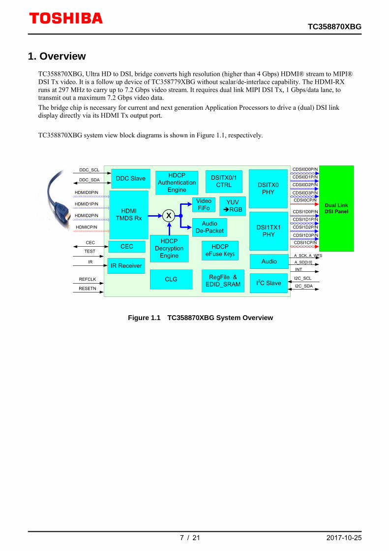
1. Overview TC358870XBG, Ultra HD to DSI, bridge converts high resolution (higher than 4 Gbps) HDMI® stream to MIPI® DSI Tx video. It is a follow up device of TC358779XBG without scalar/de-interlace capability. The HDMI-RX runs at 297 MHz to carry up to 7.2 Gbps video stream. It requires dual link MIPI DSI Tx, 1 Gbps/data lane, to transmit out a maximum 7.2 Gbps video data. The bridge chip is necessary for current and next generation Application Processors to drive a (dual) DSI link display directly via its HDMI Tx output port. TC358870XBG system view block diagrams is shown in Figure 1.1, respectively.
DDC Slave
HDCP eFuse Keys
HDMITMDS Rx
HDCP Decryption
Engine
RegFile &EDID_SRAM
Audio
AudioDe-Packet
X
DSITX0PHY
DDC_SCL
DDC_SDA
TEST
CLGREFCLK
RESETNI2C Slave
HDCPAuthentication
Engine
DSITX0/1 CTRL
I2C_SCL
I2C_SDA
CDSI0D0P/N
CDSI0CP/N
CDSI0D2P/N
CDSI0D1P/N
CDSI0D3P/N
Video FiFo
A_SD[3:0]
CEC
INT
CEC
IR ReceiverIR
DSI1TX1PHY
CDSI1D0P/N
CDSI1CP/N
CDSI1D2P/N
CDSI1D1P/N
CDSI1D3P/N
HDMID0P/N
HDMICP/N
HDMID2P/N
HDMID1P/N Dual Link DSI Panel
YUV èRGB
A_SCK, A_WFS
Figure 1.1 TC358870XBG System Overview

TC358870XBG
8 / 21 2017-10-25
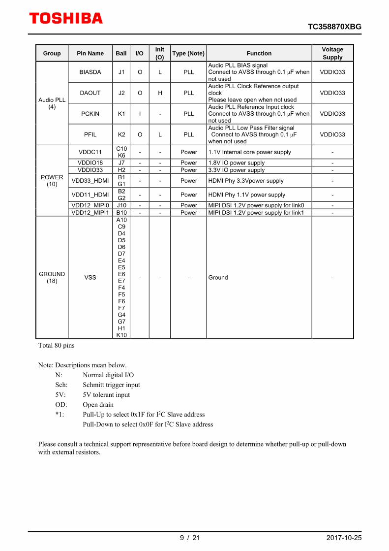
2. External Pins TC358870XBG resides in BGA80 pin packages. The following table gives the signals of TC358870XBG and their function.
Table 2.1 TC358870XBG Functional Signal List
Group Pin Name Ball I/O Init (O) Type (Note) Function Voltage
Supply
SYSTEM (4)
RESETN K8 I - Sch System reset input (active low) VDDIO18 REFCLK K9 I - Sch Reference clock input (40 – 50 MHz) VDDIO18
TEST G5 I - N Internal test terminal (Always must be fixed low externally) VDDIO18
INT J3 O L N Interrupt Output signal (active high) *1 VDDIO18
CDSI TX0 (10)
CDSI0CP F10 O H MIPI-PHY MIPI-DSI0 clock positive VDD12_MIPI0 CDSI0CN F9 O H MIPI–PHY MIPI-DSI0 clock negative VDD12_MIPI0 CDSI0D0P H10 O H MIPI–PHY MIPI-DSI0 data 0 positive VDD12_MIPI0 CDSI0D0N H9 O H MIPI–PHY MIPI-DSI0 data 0 negative VDD12_MIPI0 CDSI0D1P G10 O H MIPI–PHY MIPI-DSI0 data 1 positive VDD12_MIPI0 CDSI0D1N G9 O H MIPI–PHY MIPI-DSI0 data 1 negative VDD12_MIPI0 CDSI0D2P E10 O H MIPI–PHY MIPI-DSI0 data 2 positive VDD12_MIPI0 CDSI0D2N E9 O H MIPI–PHY MIPI-DSI0 data 2 negative VDD12_MIPI0 CDSI0D3P D10 O H MIPI–PHY MIPI-DSI0 data 3 positive VDD12_MIPI0 CDSI0D3N D9 O H MIPI–PHY MIPI-DSI0 data 3 negative VDD12_MIPI0
CDSI TX1 (10)
CDSI1CP A7 O H MIPI-PHY MIPI-DSI1 clock positive VDD12_MIPI0 CDSI1CN B7 O H MIPI–PHY MIPI-DSI1 clock negative VDD12_MIPI1 CDSI1D0P A9 O H MIPI–PHY MIPI-DSI1 data 0 positive VDD12_MIPI1 CDSI1D0N B9 O H MIPI–PHY MIPI-DSI1 data 0 negative VDD12_MIPI1 CDSI1D1P A8 O H MIPI–PHY MIPI-DSI1 data 1 positive VDD12_MIPI1 CDSI1D1N B8 O H MIPI–PHY MIPI-DSI1 data 1 negative VDD12_MIPI1 CDSI1D2P A6 O H MIPI–PHY MIPI-DSI1 data 2 positive VDD12_MIPI1 CDSI1D2N B6 O H MIPI–PHY MIPI-DSI1 data 2 negative VDD12_MIPI1 CDSI1D3P A5 O H MIPI–PHY MIPI-DSI1 data 3 positive VDD12_MIPI1 CDSI1D3N B5 O H MIPI–PHY MIPI-DSI1 data 3 negative VDD12_MIPI1
HDMI-RX (9)
HDMICP C1 I - HDMI-PHY HDMI clock channel positive VDD33_HDMI HDMICN C2 I - HDMI-PHY HDMI clock channel negative VDD33_HDMI HDMID0P D1 I - HDMI-PHY HDMI data 0 channel positive VDD33_HDMI HDMID0N D2 I - HDMI-PHY HDMI data 0 channel negative VDD33_HDMI HDMID1P E1 I - HDMI-PHY HDMI data 1 channel positive VDD33_HDMI HDMID1N E2 I - HDMI-PHY HDMI data 1 channel negative VDD33_HDMI HDMID2P F1 I - HDMI-PHY HDMI data 2 channel positive VDD33_HDMI HDMID2N F2 I - HDMI-PHY HDMI data 2 channel negative VDD33_HDMI
REXT A1 I - HDMI-PHY External reference resistor (Connect with 2kΩ to VDD33HDMI) VDD33_HDMI
DDC (2)
DDC_SCL A3 IO - Sch/5V/OD DDC I2C slave clock VDDIO33 DDC_SDA B3 IO - Sch/5V/OD DDC I2C slave data VDDIO33
CEC(1) CEC A2 IO - Sch/OD CEC signal VDDIO33
HPD(2) HPDI A4 I - 5V 5V power input VDDIO33 HPDO B4 O L N Hot plug detect output VDDIO33
Audio (7)
A_SCK K7 O L N I2S/TDM bit clock signal VDDIO18
A_WFS K5 O L N I2S word clock TDM frame sync signal VDDIO18
A_SD3 J5 O L N I2S data signal bit3 VDDIO18 A_SD2 J6 O L N I2S data signal bit2 VDDIO18 A_SD1 J8 O L N I2S data signal bit1 VDDIO18
A_SD0 J9 O L N I2S data signal bit0 TDM data signal VDDIO18
A_OSCK J4 O L N Audio Over Sampling Clock VDDIO18
IR(1) IR G6 I - N InfraRed signal (Fix low externally, if not used) VDDIO18
I2C(2) I2C_SCL K4 IO - Sch/OD I2C slave clock VDDIO18 I2C_SDA K3 IO - Sch/OD I2C slave data VDDIO18
TC358870XBG
9 / 21 2017-10-25
Group Pin Name Ball I/O Init (O) Type (Note) Function Voltage
Supply
Audio PLL (4)
BIASDA J1 O L PLL Audio PLL BIAS signal Connect to AVSS through 0.1 μF when not used
VDDIO33
DAOUT J2 O H PLL Audio PLL Clock Reference output clock Please leave open when not used
VDDIO33
PCKIN K1 I - PLL Audio PLL Reference Input clock Connect to AVSS through 0.1 μF when not used
VDDIO33
PFIL K2 O L PLL Audio PLL Low Pass Filter signal Connect to AVSS through 0.1 μF when not used
VDDIO33
POWER (10)
VDDC11 C10 K6 - - Power 1.1V Internal core power supply -
VDDIO18 J7 - - Power 1.8V IO power supply - VDDIO33 H2 - - Power 3.3V IO power supply -
VDD33_HDMI B1 G1 - - Power HDMI Phy 3.3Vpower supply -
VDD11_HDMI B2 G2 - - Power HDMI Phy 1.1V power supply -
VDD12_MIPI0 J10 - - Power MIPI DSI 1.2V power supply for link0 - VDD12_MIPI1 B10 - - Power MIPI DSI 1.2V power supply for link1 -
GROUND (18) VSS
A10 C9 D4 D5 D6 D7 E4 E5 E6 E7 F4 F5 F6 F7 G4 G7 H1 K10
- - - Ground -
Total 80 pins Note: Descriptions mean below. N: Normal digital I/O Sch: Schmitt trigger input 5V: 5V tolerant input OD: Open drain *1: Pull-Up to select 0x1F for I2C Slave address Pull-Down to select 0x0F for I2C Slave address Please consult a technical support representative before board design to determine whether pull-up or pull-down with external resistors.

TC358870XBG
10 / 21 2017-10-25
2.1. TC358870XBG 80-Pin Count Summary
Table 2.2 BGA80 Pin Count Summary Group Name Pin Count Notes
SYSTEM 4 - CDSI TX0 10 - CDSI TX1 10 - HDMI-RX 9 - DDC 2 - CEC 1 - Audio 7 - I2C 2 - IR 1 - HPD 2 - Audio PLL 4 - POWER 10 IO, Core GROUND 18 IO, Core, Analog
TOTAL Pin Count 80 Func 52 + (10+18)
2.2. Pin Layout
P-VFBGA80-0707-0.65
Top view
1 2 3 4 5 6 7 8 9 10
A A1 A2 A3 A4 A5 A6 A7 A8 A9 A10
REXT CEC DDC_SCL HPDI CDSI1D3P CDSI1D2P CDSI1CP CDSI1D1P CDSI1D0P VSS
B B1 B2 B3 B4 B5 B6 B7 B8 B9 B10
VDD33_HDMI VDD11_HDMI DDC_SDA HPDO CDSI1D3N CDSI1D2N CDSI1CN CDSI1D1N CDSI1D0N VDD12_MIPI1
C C1 C2 C3 C4 C5 C6 C7 C8 C9 C10
HDMICP HDMICN No ball No ball No ball No ball No ball No ball VSS VDDC11
D D1 D2 D3 D4 D5 D6 D7 D8 D9 D10
HDMID0P HDMID0N No ball VSS VSS VSS VSS No ball CDSI0D3N CDSI0D3P
E E1 E2 E3 E4 E5 E6 E7 E8 E9 E10
HDMID1P HDMID1N No ball VSS VSS VSS VSS No ball CDSI0D2N CDSI0D2P
F F1 F2 F3 F4 F5 F6 F7 F8 F9 F10
HDMID2P HDMID2N No ball VSS VSS VSS VSS No ball CDSI0CN CDSI0CP
G G1 G2 G3 G4 G5 G6 G7 G8 G9 G10
VDD33_HDMI VDD11_HDMI No ball VSS TEST IR VSS No ball CDSI0D1N CDSI0D1P
H H1 H2 H3 H4 H5 H6 H7 H8 H9 H10
VSS VDDIO33 No ball No ball No ball No ball No ball No ball CDSI0D0N CDSI0D0P
J J1 J2 J3 J4 J5 J6 J7 J8 J9 J10
BIASDA DAOUT INT A_OSCK A_SD3 A_SD2 VDDIO18 A_SD1 A_SD0 VDD12_MIPI0
K K1 K2 K3 K4 K5 K6 K7 K8 K9 K10
PCKIN PFIL I2C_SDA I2C_SCL A_WFS VDDC11 A_SCK RESETN REFCLK VSS
Figure 2.1 TC358870XBG 80-Pin Layout (Top View)
CDSI1
CD
SI0
HD
MI R
X A
PLL

TC358870XBG
11 / 21 2017-10-25
3. Package The 80-pin package for TC358870XBG is described in the figures below.
Figure 3.1 TC358870XBG package (P-VFBGA80-0707-0.65-001)
The mechanical dimension of BGA80 package is listed below.
Table 3.1 Mechanical Dimension
Package Solder Ball Pitch
Solder Ball Height
Package Dimension
Package Height
80-Pin 0.65 mm 0.25 mm 7.0 × 7.0 mm2 1.0 mm
(Unit: mm)
Weight: 67mg (Typ.)

TC358870XBG
12 / 21 2017-10-25
4. Electrical Characteristics
4.1. Absolute Maximum Ratings VSS= 0V reference
Item Symbol Rating Unit Supply voltage (1.8V - Digital IO) VDDIO18 -0.3 to +3.9 V
Supply voltage (3.3V - Digital IO) VDDIO33 -0.3 to +3.9 V
Supply voltage (1.1V – Digital Core) VDDC11 -0.3 to +1.8 V
Supply voltage (1.2V – MIPI DSI PHY) VDD12_MIPI -0.3 to +1.8 V
Supply voltage (3.3V – HDMIRX Phy) VDD33_HDMI -0.3 to +3.9 V
Supply voltage (1.1V – HDMIRX Phy) VDD11_HDMI -0.3 to +1.8 V
Input voltage (DSI IO) VIN_DSI -0.3 to VDD12_MIPI+0.3 V
Output voltage (DSI IO) VOUT_DSI -0.3 to VDD12_MIPI+0.3 V
Input voltage (Digital IO) VIN_IO -0.3 to VDDIO18+0.3
-0.3 to VDDIO33+0.3 V
Output voltage (Digital IO) VOUT_IO -0.3 to VDDIO18+0.3 V
Junction temperature Tj 125 oC
Storage temperature Tstg -40 to +125 oC
4.2. Operating Condition VSS= 0V reference
Item Symbol Min Typ. Max Unit Supply voltage (1.8V – Digital IO) VDDIO18 note 1.65 1.8 1.95 V Supply voltage (3.3V – Digital IO) VDDIO33 3.0 3.3 3.6 V Supply voltage (1.1V – Digital Core) VDDC11 1.1 1.15 1.2 V Supply voltage (3.3V – HDMIRX PHY) VDD33_HDMI 3.135 3.3 3.465 V Supply voltage (1.1V – HDMIRX PHY) VDD11_HDMI 1.1 1.15 1.2 V
Supply voltage (1.2V – MIPI DSI PHY) VDD12_MIPI0 VDD12_MIPI1 1.1 1.2 1.3 V
Operating temperature (ambient temperature with voltage applied) Ta -30 +25 +70 °C
Note: VDDIO18 can be used at 1.8V or 3.3V.

TC358870XBG
13 / 21 2017-10-25
4.3. DC Electrical Specification Standard IO
Item Symbol Min Max Unit
Input voltage, High level input Note1 VIH 0.70 VDDIO18 Note2 VDDIO18 Note2
V 0.61 VDDIO18 Note3 VDDIO18 Note3 0.61 VDDIO33 Note4 VDDIO33 Note4
Input voltage, Low level input Note1 VIL 0 0.30 VDDIO18 Note2
V 0.25 VDDIO18 Note3 0.25 VDDIO33 Note4
Input voltage High level CMOS Schmitt Trigger Note1 VIHS
0.70 VDDIO18 Note2 VDDIO18 Note2 V 0.61 VDDIO18 Note3 VDDIO18 Note3
0.61 VDDIO33 Note4 VDDIO33 Note4
Input voltage Low level CMOS Schmitt Trigger Note1 VILS 0
0.30 VDDIO18 Note2 V 0.25 VDDIO18 Note3
0.25 VDDIO33 Note4
Output voltage High level Note1 VOH
VDDIO18-0.45 Note2 - V VDDIO18-0.6 Note3
VDDIO33-0.6 Note4 Output voltage Low level Note1 VOL -
0.45 Note2 V 0.4 Note3 Note4
Input leak current, High level (Condition: VIN = +VDDIO, VDDIO = 3.6V) IILH1 -10 10 μA
Input leak current, Low level (Condition: VIN = 0V, VDDIO = 3.6V) IILL1 -10 10 μA
Note1: Each power source is operating within recommended operation condition. Note2: For IOs related to VDDIO18 and operated at 1.8V range. Note3: For IOs related to VDDIO18 and operated at 3.3V range. Note4: For IOs related toVDDIO33. HDMI DDC Slave IO (DDC_SDA, DDC_SCL terminal)
Item Symbol Min Max Unit Input voltage, High level input VIH 3.1 5.25 V Input voltage, Low level input VIL 0 1.7 V Output voltage Low level(IOL=8mA) VOL - 0.4 V Input leak current, High level (VIN=VDDIO33) IIH -10 10 μA
Input leak current, Low level(VIN=VSS) IIL -10 10 μA
HDMI CEC IO (CEC terminal)
Item Symbol Min Max Unit Input voltage, High level input VIH 2 VDDIO33 V Input voltage, Low level input VIL 0 0.8 V Output voltage Low level(IOL=8mA) VOL - 0.4 V Input leak current, High level(VIN=VDDIO33) IIH -10 10 μA
Input leak current, Low level(VIN=VSS) IIL -10 10 μA

TC358870XBG
14 / 21 2017-10-25
I2C IO (I2C_SDA, I2C_SCL terminal)
Item Symbol Min Max Unit Input voltage, High level input VIH 0.7VDDIO18 VDDIO18 V Input voltage, Low level input VIL 0 0.3VDDIO18 V Output voltage Low level (VDDIO18 used at 1.8V,IOL=3mA)
VOL - 0.2VDDIO18 V
Output voltage Low level (VDDIO18 used at 3.3V,IOL=3mA) - 0.4 V

TC358870XBG
15 / 21 2017-10-25
5. External Circuit Suggestion
5.1. I2C Slave address definition INT terminal is multiplexed with configuring function of I2C Slave address. During RESETN asserted, INT becomes input and detects the polarity. After RESETN deasserted it becomes INT function (output) automatically. Pull up or pull down this terminal by 10kohm resister externally. If pulled up, then I2C Slave address becomes 0x1F If pulled down then I2C Slave address becomes 0x0F
5.2. HDMI DDC_SDA and DDC_SCL are pulled up to +5V power line and +5V power line is also pulled down for DDC_SDA and DDC_SDL to be fixed low when +5V power is disabled. Below figure illustrates example DDC interface connections.
HPDI
DDC_SDA
DDC_SCL
+5V Power
SDA
SCL
Hot Plug Detect
HDMI DDC Interface
HPDO
HDMIRX_IP
47KΩ ± 5%
47KΩ ± 5%
100KΩ ± 5%
1KΩ ± 5%
Figure 5.1 Example of DDC I/F Connection
100kΩ± 5%
47kΩ± 5%
47kΩ± 5%
1kΩ± 5%

TC358870XBG
16 / 21 2017-10-25
The automatic adjustment function of terminus resistance is attached to HDMI-Rx. Therefore, connect 2kΩ±1% of reference resistance between VDD33_HDMI and REXT.
Figure 5.2 Connection of REXT resistance
5.3. Audio PLL The Audio PLL external terminal connections used in the Audio clock generation are shown in the Figure below. In DAOUT output (PLL input), a low pass filter is installed in the LSI external area. In addition, a low pass filter for cutting unnecessary components in phase comparator output in the PLL is also installed in the LSI external area.
3.3V
VDD33_HDMI
BIASDA
DAOUT
PCKIN
PFIL
Audio
PLL
VSS
GND
0.1μF±10%(B)
1.5kΩ ±5%
5pF±5% (CH)
1.0kΩ ±5%
1000pF ±10%(B)
0.1μF ±10%(B)
1.0kΩ ±5%
1000pF ±10%(B)
2SC2712Y
Figure 5.3 Audio Clock External LPF circuit block diagram
2kΩ±1%
3.3V
HDMI RX
REXT
VDD33_HDMI

TC358870XBG
17 / 21 2017-10-25
5.4. Suggestion of Power supply circuit Since the ESD protection diode is attached to the TMDS input pin between a power supply/GND, current may flow backwards HDMI-Rx from source apparatus at the time of power supply OFF. And also VDD33_HDMI power supply should be isolated from another 3.3V power supplies because this backward current also damages them. Below figure is recommend attaching a back flow prevention circuit. Case (1) External switch circuit Attach the adverse current prevention switch from a TMDS differential signal. Since reverse current also gives damage to VDDIO33, this switch shall separate VDD33_HDMI and VDDIO33.
3.3V Reg.
1.15V Reg.
>1μF
>1μF
>0.1μF
>0.1μF
VDD33_HDMI
VSS
VDD11_HDMI
TMDS Signal
VDDIO33
>10μF
>10μF
TMDS Rx
DDC SlaveCEC
Audio PLL
VSS
>1μF >0.1μF
VDDIO18 SystemAudio
IRI2C Slave
>1μF >0.1μF
1.8V Reg.
FB
FB
FB
FB
>10μF
MIPI
VSS
FB
VDDC11
>1μF >0.1μF
FB
1.2V Reg.
>10μF
VSS
VDD12_MIPI0
>1μF >0.1μFFB
VDD12_MIPI1
>10μF
5V
>10μF
>10μF
>10μF
>10μF
ENEN
OUTIN
GN
DG
ND
OUTIN
OUTIN
GN
DG
ND
OUTIN
All TC358870 VSSs should be separated at AC level from regulators’ VSS with FB(ferrite bead) or another method to attenuate EMI.
Figure 5.4 Suggestion of power supply circuit with external switch

TC358870XBG
18 / 21 2017-10-25
Case (2) Regulator with reverse current protection Apply a current protection regulator to VDD33_HDMI.
1.15V Reg.
>1μF
>1μF
>0.1μF
>0.1μF
VDD33_HDMI
VSS
VDD11_HDMI
TMDS Signal
VDDIO33
>10μF
>10μF
TMDS Rx
DDC SlaveCEC
Audio PLL
VSS
>1μF >0.1μF
VDDIO18 SystemAudio
IRI2C Slave
>1μF >0.1μF
1.8V Reg.
FB
FB
FB
FB
MIPI
VSS
FB
VDDC11
>1μF >0.1μF
FB
1.2V Reg.
>10μF
VSS
VDD12_MIPI0
>1μF >0.1μFFB
VDD12_MIPI1
>10μF
>10μF
5V
>10μF
>10μF
>10μF
>10μF
3.3V Reg.
ENEN
3.3V Reg.Reverse Current
Protection
EN
OUTIN
GN
DG
ND
OUTIN
>10μF
IN OUT
GN
D
IN OUT
IN OUT
GN
DG
ND
All TC358870 VSSs should be separated at AC level from regulators’ VSS with FB(ferrite bead) or another method to attenuate EMI.
Figure 5.5 Suggestion of power supply circuit with current protection regulator

TC358870XBG
19 / 21 2017-10-25
Case (3) Use of VDDIO18 at 3.3V range If VDDIO is applied at 3.3V range, Common regulation is available among VDD33_HDMI, VDIO33 and VDDIO18. Attach the adverse current prevention switch from a TMDS differential signal. Since reverse current also gives damage to VDDIO33 and VDDIO18, this switch shall separate VDD33_HDMI and VDDIO33/VDDIO18.
3.3V Reg.
1.15V Reg.
>1μF
>1μF
>0.1μF
>0.1μF
VDD33_HDMI
VSS
VDD11_HDMI
TMDS Signal
VDDIO33
>10μF
TMDS Rx
DDC SlaveCEC
Audio PLL
VSS
>1μF >0.1μF
VDDIO18 SystemAudio
IRI2C Slave
>1μF >0.1μF
FB
FB
FB
FB
>10μF
MIPI
VSS
FB
VDDC11
>1μF >0.1μF
FB
1.2V Reg.
>10μF
VSS
VDD12_MIPI0
>1μF >0.1μFFB
VDD12_MIPI1
>10μF
5V
IN
IN
IN
>10μF
>10μF
EN
OUT
GN
D
OUT
GN
D
OUT
GN
D
>10μF
All TC358870 VSSs should be separated at AC level from regulators’ VSS with FB(ferrite bead) or another method to attenuate EMI.
Figure 5.6 Suggestion of power supply circuit at VDDIO18 = 3.3V

TC358870XBG
20 / 21 2017-10-25
6. Revision History Table 6.1 Revision History
Revision Date Description 1.0 2014-08-01 New
1.1 2014-09-18
Remove registers 0x5008 and 0x5088 which are not used Remove Supply Noise Voltage, VSN, from Operation Condition table in section 8.2 Typo fixed 0x04_10 => 0x8410 Add more descriptions for 0x025C, 0x026C, NCO_48F, NCO_44F Remove “address 0x85_0F” and adding note
1.521 2015-12-18 Typo Init(O) DAOUT pin in External Pins
1.522 2016-04-01 ・Modified the weight of TC358870XBG’s package by rounding up digits after the decimal point to form an integer.
1.53 2017-10-25 Added comment to HDCP in Features. Changed header, footer and the last page. Changed corporate name.

TC358870XBG
21 / 21 2017-10-25
RESTRICTIONS ON PRODUCT USE Toshiba Corporation and its subsidiaries and affiliates are collectively referred to as “TOSHIBA”. Hardware, software and systems described in this document are collectively referred to as “Product”.
• TOSHIBA reserves the right to make changes to the information in this document and related Product without notice.
• This document and any information herein may not be reproduced without prior written permission from TOSHIBA. Even with TOSHIBA's written permission, reproduction is permissible only if reproduction is without alteration/omission.
• Though TOSHIBA works continually to improve Product's quality and reliability, Product can malfunction or fail. Customers are responsible for complying with safety standards and for providing adequate designs and safeguards for their hardware, software and systems which minimize risk and avoid situations in which a malfunction or failure of Product could cause loss of human life, bodily injury or damage to property, including data loss or corruption. Before customers use the Product, create designs including the Product, or incorporate the Product into their own applications, customers must also refer to and comply with (a) the latest versions of all relevant TOSHIBA information, including without limitation, this document, the specifications, the data sheets and application notes for Product and the precautions and conditions set forth in the "TOSHIBA Semiconductor Reliability Handbook" and (b) the instructions for the application with which the Product will be used with or for. Customers are solely responsible for all aspects of their own product design or applications, including but not limited to (a) determining the appropriateness of the use of this Product in such design or applications; (b) evaluating and determining the applicability of any information contained in this document, or in charts, diagrams, programs, algorithms, sample application circuits, or any other referenced documents; and (c) validating all operating parameters for such designs and applications. TOSHIBA ASSUMES NO LIABILITY FOR CUSTOMERS' PRODUCT DESIGN OR APPLICATIONS.
• PRODUCT IS NEITHER INTENDED NOR WARRANTED FOR USE IN EQUIPMENTS OR SYSTEMS THAT REQUIRE EXTRAORDINARILY HIGH LEVELS OF QUALITY AND/OR RELIABILITY, AND/OR A MALFUNCTION OR FAILURE OF WHICH MAY CAUSE LOSS OF HUMAN LIFE, BODILY INJURY, SERIOUS PROPERTY DAMAGE AND/OR SERIOUS PUBLIC IMPACT ("UNINTENDED USE"). Except for specific applications as expressly stated in this document, Unintended Use includes, without limitation, equipment used in nuclear facilities, equipment used in the aerospace industry, medical equipment, equipment used for automobiles, trains, ships and other transportation, traffic signaling equipment, equipment used to control combustions or explosions, safety devices, elevators and escalators, devices related to electric power, and equipment used in finance-related fields. IF YOU USE PRODUCT FOR UNINTENDED USE, TOSHIBA ASSUMES NO LIABILITY FOR PRODUCT. For details, please contact your TOSHIBA sales representative.
• Do not disassemble, analyze, reverse-engineer, alter, modify, translate or copy Product, whether in whole or in part.
• Product shall not be used for or incorporated into any products or systems whose manufacture, use, or sale is prohibited under any applicable laws or regulations.
• The information contained herein is presented only as guidance for Product use. No responsibility is assumed by TOSHIBA for any infringement of patents or any other intellectual property rights of third parties that may result from the use of Product. No license to any intellectual property right is granted by this document, whether express or implied, by estoppel or otherwise.
• ABSENT A WRITTEN SIGNED AGREEMENT, EXCEPT AS PROVIDED IN THE RELEVANT TERMS AND CONDITIONS OF SALE FOR PRODUCT, AND TO THE MAXIMUM EXTENT ALLOWABLE BY LAW, TOSHIBA (1) ASSUMES NO LIABILITY WHATSOEVER, INCLUDING WITHOUT LIMITATION, INDIRECT, CONSEQUENTIAL, SPECIAL, OR INCIDENTAL DAMAGES OR LOSS, INCLUDING WITHOUT LIMITATION, LOSS OF PROFITS, LOSS OF OPPORTUNITIES, BUSINESS INTERRUPTION AND LOSS OF DATA, AND (2) DISCLAIMS ANY AND ALL EXPRESS OR IMPLIED WARRANTIES AND CONDITIONS RELATED TO SALE, USE OF PRODUCT, OR INFORMATION, INCLUDING WARRANTIES OR CONDITIONS OF MERCHANTABILITY, FITNESS FOR A PARTICULAR PURPOSE, ACCURACY OF INFORMATION, OR NONINFRINGEMENT.
• Do not use or otherwise make available Product or related software or technology for any military purposes, including without limitation, for the design, development, use, stockpiling or manufacturing of nuclear, chemical, or biological weapons or missile technology products (mass destruction weapons). Product and related software and technology may be controlled under the applicable export laws and regulations including, without limitation, the Japanese Foreign Exchange and Foreign Trade Law and the U.S. Export Administration Regulations. Export and re-export of Product or related software or technology are strictly prohibited except in compliance with all applicable export laws and regulations.
• Please contact your TOSHIBA sales representative for details as to environmental matters such as the RoHS compatibility of Product. Please use Product in compliance with all applicable laws and regulations that regulate the inclusion or use of controlled substances, including without limitation, the EU RoHS Directive. TOSHIBA ASSUMES NO LIABILITY FOR DAMAGES OR LOSSES OCCURRING AS A RESULT OF NONCOMPLIANCE WITH APPLICABLE LAWS AND REGULATIONS.

Mouser Electronics
Authorized Distributor
Click to View Pricing, Inventory, Delivery & Lifecycle Information: Toshiba:
TC358870XBG(NOK)