tdc1011 ultrasonic sensing analog front end (afe) … single channel ultrasonic sensing analog front...
TRANSCRIPT

Product
Folder
Sample &Buy
Technical
Documents
Tools &
Software
Support &Community
ReferenceDesign
TDC1011SNAS662 –JULY 2015
TDC1011 Single Channel Ultrasonic Sensing Analog Front End (AFE) for Level Sensing,Concentration Sensing Applications
1 Features 3 DescriptionThe TDC1011 is a fully integrated analog front-end
1• Measurement Range: Up to 8 ms(AFE) for ultrasonic sensing measurements of liquid• Operating Current: 1.8 µA (2 SPS) level, fluid identification/concentration, and proximity/
• Transmitter Channel TX distance applications common in automotive,industrial, medical, and consumer markets. When– Supports Single Transducer Applicationspaired with an MSP430/C2000 MCU, power, wireless,– Programmable Excitation: 31.25 kHz to 4 MHz, and source code, TI provides the complete ultrasonicUp to 31 Pulses sensing solution.
• Receiver Channel RXTI's Ultrasonic AFE offers programmability and
– STOP Cycle-to-Cycle Jitter: 50 psRMS flexibility to accommodate a wide-range of– Low-Noise and Programmable Gain Amplifiers applications and end equipment. The TDC1011 can
be configured for multiple transmit pulses and– Access to Signal Chain for External Filterfrequencies, gain, and signal thresholds for use withDesigna wide-range of transducer frequencies (31.25kHz to
– Programmable Threshold Comparator for Echo 4MHz) and Q-factors. Similarly, the programmabilityQualification of the receive path allows ultrasonic waves to be
detected over a wider range of distances/tank sizes– Programmable Low Power Mode for Long TOFand through various mediums.Measurements
• Temperature Measurement Selecting different modes of operation, the TDC1011can be optimized for low power consumption, making– Interface to Two PT1000/500 RTDsit ideal for battery powered applications. The low– RTD-to-RTD Matching Accuracy 0.02°CRMS noise amplifiers and comparators provide extremely
• Operating Temperature Range: -40°C to 125°C low jitter, enabling picosecond resolution andaccuracy.
2 ApplicationsDevice Information(1)
• Measurements Through Tanks of VaryingPART NUMBER PACKAGE BODY SIZE (NOM)Materials:
TDC1011 TSSOP (PW-28) 9.70 mm × 4.40 mm– Fluid Level(1) For all available packages, see the orderable addendum at– Fluid Identification / Concentration the end of the data sheet.
1
An IMPORTANT NOTICE at the end of this data sheet addresses availability, warranty, changes, use in safety-critical applications,intellectual property matters and other important disclaimers. PRODUCTION DATA.

TDC1011SNAS662 –JULY 2015 www.ti.com
Table of Contents8.3 Feature Description................................................. 121 Features .................................................................. 18.4 Device Function Description ................................... 192 Applications ........................................................... 18.5 Programming .......................................................... 283 Description ............................................................. 18.6 Register Maps ......................................................... 304 Revision History..................................................... 2
9 Application and Implementation ........................ 365 Pin Configuration and Functions ......................... 39.1 Application Information............................................ 366 Specifications......................................................... 49.2 Typical Applications ................................................ 366.1 Absolute Maximum Ratings ...................................... 4
10 Power Supply Recommendations ..................... 416.2 ESD Ratings ............................................................ 411 Layout................................................................... 426.3 Recommended Operating Conditions....................... 4
11.1 Layout Guidelines ................................................. 426.4 Thermal Information .................................................. 411.2 Layout Example .................................................... 426.5 Electrical Characteristics........................................... 5
12 Device and Documentation Support ................. 436.6 Timing Requirements ................................................ 712.1 Device Support...................................................... 436.7 Switching Characteristics .......................................... 712.2 Community Resources.......................................... 436.8 Typical Characteristics .............................................. 812.3 Trademarks ........................................................... 437 Parameter Measurement Information ................ 1012.4 Electrostatic Discharge Caution............................ 438 Detailed Description ............................................ 1112.5 Glossary ................................................................ 438.1 Overview ................................................................. 11
13 Mechanical, Packaging, and Orderable8.2 Functional Block Diagram ....................................... 11Information ........................................................... 43
4 Revision History
DATE REVISION NOTESJuly 2015 * Initial release.
2 Submit Documentation Feedback Copyright © 2015, Texas Instruments Incorporated
Product Folder Links: TDC1011

NC
RX
VCOM
PGAIN
PGAOUT
TX
NC
GND
CLKIN
COMPIN
RTD1
RTD2
VIO
SDO
RREF
RES
ERRB
SDI
CSB
SCLK
START
STOP
LNAOUT
RESET
TRIGGER
EN
VDD
VDD
23
1
4567
98
1011121314
2726
28
25242322
2021
1918171615
TD
C1011
TDC1011www.ti.com SNAS662 –JULY 2015
5 Pin Configuration and Functions
TSSOP(PW) 28 Pin
Top View
Pin FunctionsPIN
TYPE (1) DESCRIPTIONNAME NO.
NC 1 No Connect (leave floating)RX 2 I Receive inputVCOM 3 P Output common mode voltage biasLNAOUT 4 O Low noise amplifier output (for ac decoupling capacitor)PGAIN 5 I Programmable gain amplifier inputPGAOUT 6 O Programmable gain amplifier outputCOMPIN 7 I Echo qualification and zero-crossing detector inputRTD1 8 O Resistance temperature detector channel 1RTD2 9 O Resistance temperature detector channel 2RREF 10 O Reference resistor for temperature measurementRES 11 I Reserved (connect to GND)ERRB 12 O Error flag (open drain)START 13 O Start pulse outputSTOP 14 O Stop pulse outputEN 15 I Enable (active high; when low the TDC1011 is in SLEEP mode)TRIGGER 16 I Trigger inputRESET 17 I Reset (active high)SCLK 18 I Serial clock for the SPI interfaceCSB 19 I Chip select for the SPI interface (active low)SDI 20 I Serial data input for the SPI interfaceSDO 21 O Serial data output for the SPI interfaceVIO 22 P Positive I/O supplyVDD 23, 24 P Positive supply; all VDD supply pins must be connected to the supply. Place a 100-nF bypass capacitor
to ground in close proximity to the pin.CLKIN 25 I Clock inputGND 26 G Negative supplyNC 27 No Connect (leave floating)TX 28 O Transmit output
(1) G = Ground, I = Input, O = Output, P = Power
Copyright © 2015, Texas Instruments Incorporated Submit Documentation Feedback 3
Product Folder Links: TDC1011

TDC1011SNAS662 –JULY 2015 www.ti.com
6 Specifications
6.1 Absolute Maximum RatingsOver operating free-air temperature range (unless otherwise noted) (1) (2)
MIN MAX UNITVDD Analog supply voltage, VDD pins –0.3 6.0 VVIO I/O supply voltage (VIO must always be lower than or equal to VDD supply) –0.3 6.0 VVI Voltage on any analog input pin (3) –0.3 VDD + 0.3 VVI Voltage on any digital input pin (3) –0.3 VIO + 0.3 VII Input current at any pin 5 mATJ Operating junction temperature –40 125 °CTstg Storage temperature range –65 150 °C
(1) Stresses beyond those listed under Absolute Maximum Ratings may cause permanent damage to the device. These are stress ratingsonly, which do not imply functional operation of the device at these or any other conditions beyond those indicated under RecommendedOperating Conditions. Exposure to absolute-maximum-rated conditions for extended periods may affect device reliability.
(2) All voltages are with respect to ground, unless otherwise specified.(3) When the input voltage at a pin exceeds the power supplies, the current at that pin must not exceed 5 mA and the voltage (VI) at that
pin must not exceed 6.0 V.
6.2 ESD RatingsVALUE UNIT
Human-body model (HBM), per AEC A100-002 (1) ±2000All pins ±500V(ESD) Electrostatic discharge VCharged-device model (CDM), per AECCorner pins (1, 14, 15Q100-011 ±750and 28)
(1) AEC Q100-002 indicates HBM stressing is done in accordance with the ANSI/ESDA/JEDEC JS-001 specification.
6.3 Recommended Operating ConditionsOver operating free-air temperature range (unless otherwise noted)
MIN MAX UNITVDD Analog supply voltage, VDD pins 2.7 5.5 VVIO Digital supply voltage, (VIO must always be lower than or equal to VDD supply) 1.8 VDD VVI Voltage on any analog input pin GND VDD VVI Voltage on any digital input pin GND VIO VƒCLKIN Operating frequency 0.06 16 MHzTJ Operating junction temperature –40 125 °C
6.4 Thermal Information (1)
TDC1011THERMAL METRIC TSSOP UNIT
PW (28 PINS)RθJA Junction-to-ambient thermal resistance 83.5RθJC(top) Junction-to-case (top) thermal resistance 29.9RθJB Junction-to-board thermal resistance 40.8 °C/WψJT Junction-to-top characterization parameter 2.4ψJB Junction-to-board characterization parameter 40.3
(1) For more information about traditional and new thermal metrics, see the IC Package Thermal Metrics application report, SPRA953.
4 Submit Documentation Feedback Copyright © 2015, Texas Instruments Incorporated
Product Folder Links: TDC1011
TDC1011www.ti.com SNAS662 –JULY 2015
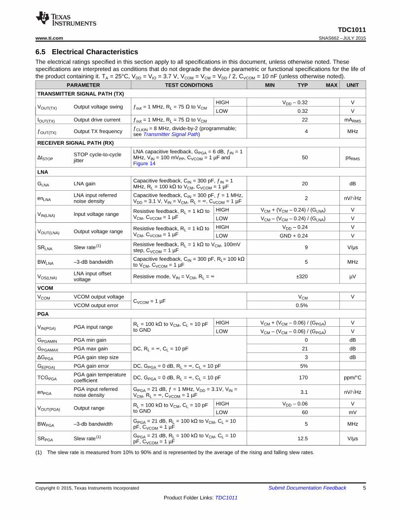
6.5 Electrical CharacteristicsThe electrical ratings specified in this section apply to all specifications in this document, unless otherwise noted. Thesespecifications are interpreted as conditions that do not degrade the device parametric or functional specifications for the life ofthe product containing it. TA = 25°C, VDD = VIO = 3.7 V, VCOM = VCM = VDD / 2, CVCOM = 10 nF (unless otherwise noted).
PARAMETER TEST CONDITIONS MIN TYP MAX UNITTRANSMITTER SIGNAL PATH (TX)
HIGH VDD – 0.32 VVOUT(TX) Output voltage swing ƒout = 1 MHz, RL = 75 Ω to VCM LOW 0.32 VIOUT(TX) Output drive current ƒout = 1 MHz, RL = 75 Ω to VCM 22 mARMS
ƒCLKIN = 8 MHz, divide-by-2 (programmable;ƒOUT(TX) Output TX frequency 4 MHzsee Transmitter Signal Path)RECEIVER SIGNAL PATH (RX)
LNA capacitive feedback, GPGA = 6 dB, ƒIN = 1STOP cycle-to-cycleΔtSTOP MHz, VIN = 100 mVPP, CVCOM = 1 µF and 50 psRMSjitter Figure 14LNA
Capacitive feedback, CIN = 300 pF, ƒIN = 1GLNA LNA gain 20 dBMHz, RL = 100 kΩ to VCM, CVCOM = 1 µFLNA input referred Capacitive feedback, CIN = 300 pF, ƒ = 1 MHz,enLNA 2 nV/√Hznoise density VDD = 3.1 V, VIN = VCM, RL = ∞, CVCOM = 1 µF
HIGH VCM + (VCM – 0.24) / (GLNA) VResistive feedback, RL = 1 kΩ toVIN(LNA) Input voltage range VCM, CVCOM = 1 µF LOW VCM – (VCM – 0.24) / (GLNA) VHIGH VDD – 0.24 VResistive feedback, RL = 1 kΩ toVOUT(LNA) Output voltage range VCM, CVCOM = 1 µF LOW GND + 0.24 V
Resistive feedback, RL = 1 kΩ to VCM, 100mVSRLNA Slew rate (1) 9 V/μsstep, CVCOM = 1 µFCapacitive feedback, CIN = 300 pF, RL= 100 kΩBWLNA –3-dB bandwidth 5 MHzto VCM, CVCOM = 1 µF
LNA input offsetVOS(LNA) Resistive mode, VIN = VCM, RL = ∞ ±320 µVvoltageVCOMVCOM VCOM output voltage VCM V
CVCOM = 1 µFVCOM output error 0.5%
PGAHIGH VCM + (VCM – 0.06) / (GPGA) VRL = 100 kΩ to VCM, CL = 10 pFVIN(PGA) PGA input range to GND LOW VCM – (VCM – 0.06) / (GPGA) V
GPGAMIN PGA min gain 0 dBGPGAMAX PGA max gain DC, RL = ∞, CL = 10 pF 21 dBΔGPGA PGA gain step size 3 dBGE(PGA) PGA gain error DC, GPGA = 0 dB, RL = ∞, CL = 10 pF 5%
PGA gain temperatureTCGPGA DC, GPGA = 0 dB, RL = ∞, CL = 10 pF 170 ppm/°CcoefficientPGA input referred GPGA = 21 dB, ƒ = 1 MHz, VDD = 3.1V, VIN =enPGA 3.1 nV/√Hznoise density VCM, RL = ∞, CVCOM = 1 µF
HIGH VDD – 0.06 VRL = 100 kΩ to VCM, CL = 10 pFVOUT(PGA) Output range to GND LOW 60 mVGPGA = 21 dB, RL = 100 kΩ to VCM, CL = 10BWPGA –3-db bandwidth 5 MHzpF, CVCOM = 1 µFGPGA = 21 dB, RL = 100 kΩ to VCM, CL = 10SRPGA Slew rate (1) 12.5 V/µspF, CVCOM = 1 µF
(1) The slew rate is measured from 10% to 90% and is represented by the average of the rising and falling slew rates.
Copyright © 2015, Texas Instruments Incorporated Submit Documentation Feedback 5
Product Folder Links: TDC1011

TDC1011SNAS662 –JULY 2015 www.ti.com
Electrical Characteristics (continued)The electrical ratings specified in this section apply to all specifications in this document, unless otherwise noted. Thesespecifications are interpreted as conditions that do not degrade the device parametric or functional specifications for the life ofthe product containing it. TA = 25°C, VDD = VIO = 3.7 V, VCOM = VCM = VDD / 2, CVCOM = 10 nF (unless otherwise noted).
PARAMETER TEST CONDITIONS MIN TYP MAX UNITZERO CROSS COMPARATORVOS(COMP) Input offset voltage (2) Referred to VCOM ±115 µV
Zero crossingenCOMP comparator input 1 MHz 5 nV/√Hz
referred noise (2)
HYSTCOMP Hysteresis (2) Referred to VCOM -10 mVTHRESHOLD DETECTOR
ECHO_QUAL_THLD = 0h, VCOM referred –35 mVVTHDET Threshold level
ECHO_QUAL_THLD = 7h, VCOM referred –1.5 VTEMPERATURE SENSOR INTERFACE (3)
RREF = 1 kΩ, PT1000 range: –40 to 125°C (4) 1 °CTemperatureTERROR measurement accuracy RREF = 1 kΩ, PT1000 range: –15°C to 85°C (4) 0.5 °CRelative accuracy RREF = 1 kΩ, RRTD1 = RRTD2 = 1.1 kΩ 0.02 °CRMS
TGE Gain error 5.8 m°C/°CPOWER SUPPLY
Sleep (EN = CLKIN = TRIGGER = low) 0.61 µAContinuous receive mode, LNA and PGA 2.8 3 mAbypassed
IDD VDD supply current Continuous receive mode, LNA and PGA active 6.2 7.5 mATemp. measurement only (PT1000 mode) (5) 370 400 µATemp. measurement (PT500 mode) (6) 500 540 µA
VIO supply sleepIIO Sleep (EN = CLKIN = TRIGGER = low) 2 nAcurrent (2)
DIGITAL INPUT/OUTPUT CHARACTERISTICSInput logic lowVIL 0.2 × VIO VthresholdInput logic highVIH 0.8 × VIO Vthreshold
SDO pin, 100-μA current 0.2 VSDO pin, 1.85-mA current 0.4 VSTART and STOP pins, 100-μA current 0.5 VOutput logic lowVOL threshold START and STOP pins, 1.85-mA current 0.6 VERRB pin, 100-μA current 0.2 VERRB pin, 1.85-mA current 0.4 VSDO pin, 100-μA current VIO – 0.2 VSDO pin, 1.85-mA current VIO – 0.6 V
Output logic highVOH START and STOP pins, 100-μA current VIO – 0.5 VthresholdSTART and STOP pins, 1.85-mA current VIO – 0.6 VERRB pin, 0-µA current VIO – 0.2 V
Maximum outputIOMAX current for SDO, 1.85 mA
START and STOP
(2) Specified by design.(3) With ideal external components. For more detail see Temp Sensor Measurement section.(4) PT1000 RTD approximate resistance: 800 Ω ≡ –52°C, 931 Ω ≡ –18°C, 1.10 kΩ ≡ 26°C, 1.33 kΩ ≡ 86°C and 1.48 kΩ ≡ 125°C.(5) Specified currents include 120μA which flows through the RTD sensor in PT1000 mode (TEMP_RTD_SEL = 0).(6) Specified currents include 240μA which flows through the RTD sensor in PT500 mode (TEMP_RTD_SEL = 1).
6 Submit Documentation Feedback Copyright © 2015, Texas Instruments Incorporated
Product Folder Links: TDC1011

t7
t8
t3t2 t1
t4 t5
t6
D15 D0D14
SCLK
CSB
Prior D15
t9
Prior D1 Prior D0
90%
10%
tr
90%
10%
tf
TDC1011www.ti.com SNAS662 –JULY 2015
6.6 Timing RequirementsTA = 25°C, VDD = VIO = 3.7 V and ƒSCLK = 1 MHz (unless otherwise noted).
MIN NOM MAX UNITƒSCLK Serial clock frequency 26 MHzt1 High period, SCLK 16 nst2 Low period, SCLK 16 nst3 Set-up time, nCS to SCLK 10 nst4 Set-up time, SDI to SCLK 12 nst5 Hold time, SCLK to SDI 12 nst6 SCLK transition to SDO valid time 16 nst7 Hold time, SCLK transition to nCS rising edge 10 nst8 nCS inactive 17 nst9 Hold time, SCLK transition to nCS falling edge 10 nstr / tf Signal rise and fall times (1) 1.8 ns
(1) The slew rate is measured from 10% to 90% and is represented by the average of the rising and falling slew rates.
Figure 1. SPI Timing Diagram
6.7 Switching CharacteristicsTA = 25°C, VDD = VIO = 3.7 V, ƒCLKIN = 8 MHz.
PARAMETER TEST CONDITIONS MIN TYP MAX UNITSTART, STOP, ENABLE, RESET, CLOCKIN, TRIGGER, ERR
TX_FREQ_DIV = 2h, NUM_TX = 1 1 μsPWSTART Pulse width for START signal TX_FREQ_DIV = 2h, NUM_TX = 2 2 μs
TX_FREQ_DIV = 2h, NUM_TX ≥ 3 3 μstr / tf Rise/fall time for START 20% to 80%, 20-pF load 0.25 nsSTART signaltr / tf STOP Rise/fall time for STOP signal 20% to 80%, 20-pF load 0.25 ns
Maximum CLKIN inputƒCLKIN 16 MHzfrequencytr / tf CLKIN CLKIN input rise/fall time (1) 20% to 80% 10 ns
TRIGGER input rise/falltr / tf TRIG 20% to 80% 10 nstime (1)
tEN_TRIG Enable to trigger wait time (1) 50 nsTX_FREQ_DIV = 2h (see TX/RX MeasurementtRES_TRIG Reset to trigger wait time (1) 3.05 μsSequencing and Timing)
(1) Specified by design.
Copyright © 2015, Texas Instruments Incorporated Submit Documentation Feedback 7
Product Folder Links: TDC1011
Out
put
Vol
tage
(25
0mV
/DIV
)
Time (1s/DIV)
C005
Out
put
Vol
tage
(25
0mV
/DIV
)
Time (1s/DIV)
C006
5k 50k 500k 2M 0
1
2
3
4
5
6
7
8
9
10
Inpu
t-re
ferr
ed N
oise
(nV
/O,Ì
Frequency (Hz) C013
5k 50k 500k 2M 0
1
2
3
4
5
6
7
8
9
10
Inpu
t-re
ferr
ed N
oise
(nV
/O,Ì
Frequency (Hz) C014
100 1k 10k 100k 1M 10M ±100
0
100
200
300
400
500
Out
put
Impe
danc
e M
agni
tude
(|
|)
Frequency (Hz) C001
100 1k 10k 100k 1M 10M ±100
0
100
200
300
400
500
Out
put
Impe
danc
e M
agni
tude
(|_
Frequency (Hz) C002
TDC1011SNAS662 –JULY 2015 www.ti.com
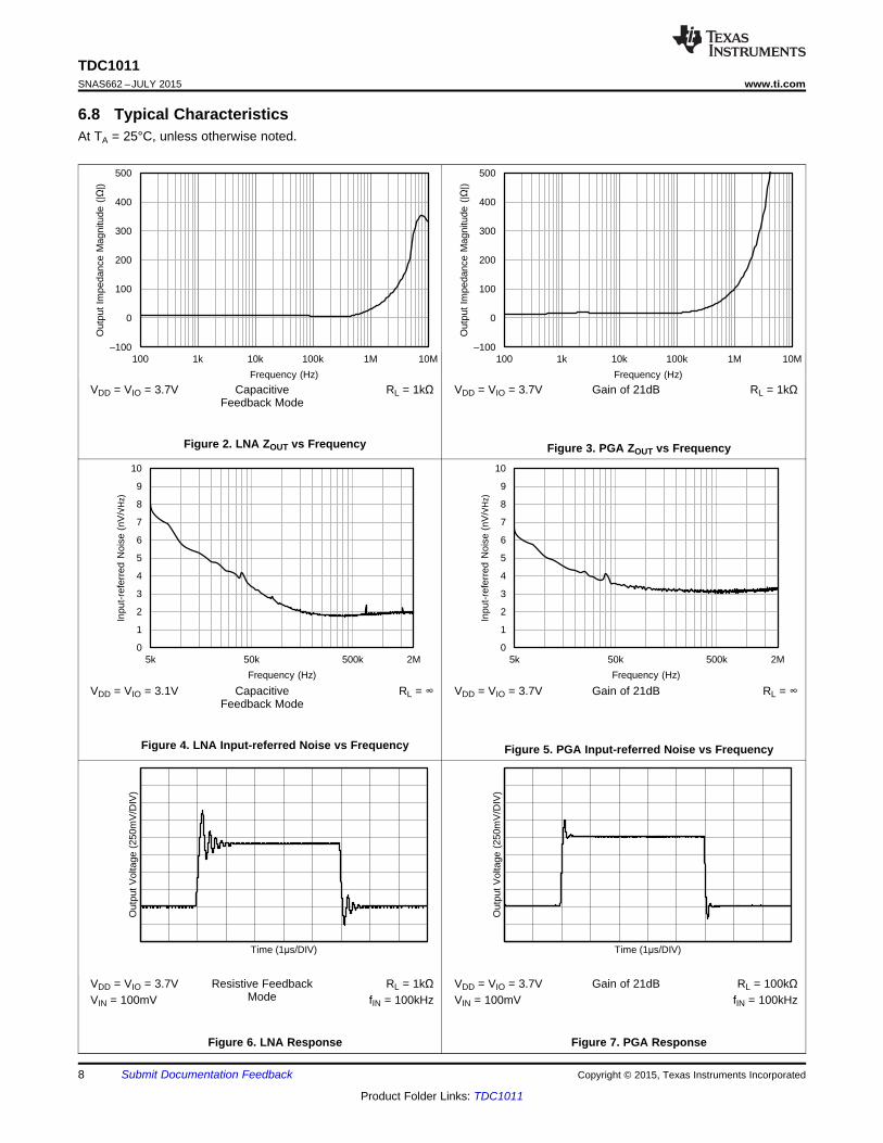
6.8 Typical CharacteristicsAt TA = 25°C, unless otherwise noted.
VDD = VIO = 3.7V Capacitive RL = 1kΩ VDD = VIO = 3.7V Gain of 21dB RL = 1kΩFeedback Mode
Figure 2. LNA ZOUT vs Frequency Figure 3. PGA ZOUT vs Frequency
VDD = VIO = 3.1V Capacitive RL = ∞ VDD = VIO = 3.7V Gain of 21dB RL = ∞Feedback Mode
Figure 4. LNA Input-referred Noise vs Frequency Figure 5. PGA Input-referred Noise vs Frequency
VDD = VIO = 3.7V Resistive Feedback RL = 1kΩ VDD = VIO = 3.7V Gain of 21dB RL = 100kΩModeVIN = 100mV fIN = 100kHz VIN = 100mV fIN = 100kHz
Figure 6. LNA Response Figure 7. PGA Response
8 Submit Documentation Feedback Copyright © 2015, Texas Instruments Incorporated
Product Folder Links: TDC1011

0
2
4
6
8
10
12
14
16
18
20
-300
-200
-100 0
100
200
300
Cou
nt (
%)
Time (ps) C011
0
2
4
6
8
10
12
14
16
18
20
-300
-200
-100 0
100
200
300
Cou
nt (
%)
Time (ps) C012
0
2
4
6
8
10
12
14
16
18
20
-300
-200
-100 0
100
200
300
Cou
nt (
%)
Time (ps) C009
0
2
4
6
8
10
12
14
16
18
20
-300
-200
-100 0
100
200
300
Cou
nt (
%)
Time (ps) C010
10k 100k 1M 10M ±30
±20
±10
0
10
20
30
Gai
n (d
B)
Frequency (Hz) C007
10k 100k 1M 10M ±30
±20
±10
0
10
20
30
Gai
n (d
B)
Frequency (Hz) C008
TDC1011www.ti.com SNAS662 –JULY 2015
Typical Characteristics (continued)At TA = 25°C, unless otherwise noted.
VDD = VIO = 3.7V Capacitive RL = 100kΩ VDD = VIO = 3.7V Gain of 21dB RL = 100kΩFeedback Mode
CIN = 300 pF
Figure 8. LNA Gain vs Frequency Figure 9. PGA Gain vs Frequency
VDD = VIO = 5V LNA Capacitive PGA Gain of 6dB VDD = VIO = 3.7V LNA Capacitive PGA Gain of 6dBFeedback Mode Feedback ModeVIN = 100mV fIN = 1MHz VIN = 100mV fIN = 1MHz(See Figure 14) Count >= 10000 TA = 25C° (See Figure 14) Count >= 10000
Figure 10. RX Jitter Histogram Figure 11. RX Jitter Histogram
VDD = VIO = 3.7V LNA Capacitive PGA Gain of 6dB VDD = VIO = 3.7V LNA Capacitive PGA Gain of 6dBFeedback Mode Feedback ModeVIN = 100mV fIN = 1MHz VIN = 100mV fIN = 1MHz
TA = -40C° (See Figure 14) Count >= 10000 TA = 125C° (See Figure 14) Count >= 10000
Figure 12. RX Jitter Histrogam Figure 13. RX Jitter Histogram
Copyright © 2015, Texas Instruments Incorporated Submit Documentation Feedback 9
Product Folder Links: TDC1011

COMPIN
GND
RF1 = 1 N CF2 = 51 pF
CF3 = 51 pF
VCOM
RF2 = 5.1 N
PGAOUT
INPUT
CIN = 300 pF
LNAIN
LNAOUT
CF1 = 1 nF
PGAIN
TDC1011SNAS662 –JULY 2015 www.ti.com
7 Parameter Measurement Information
Figure 14. External Circuits for Jitter Measurement
10 Submit Documentation Feedback Copyright © 2015, Texas Instruments Incorporated
Product Folder Links: TDC1011

Threshold Detect
Zero-Cross Detect
VC
OM
GN
D
RR
EF
RT
D2
RT
D1
START
STOP
SD
O
SD
I
SC
LK
CS
B
EN
CLK
IN
PG
AIN
PG
AO
UT
CO
MP
IN
ER
RB
VIO
VD
D
TDC1011
RX
MU
XM
UX
LNA±
+ ±
+
LNA
OU
T
enable
DAC
Temp. Sense
20 dB 0 to 21 dB
TR
IGG
ER
RE
SE
T
RE
S
VD
D
VCOM
VCOM
Clock Divider
SM ControlUnit
SerialInterface
EventManager
Analog Bias
PGA
TXTx
Generator
TDC1011www.ti.com SNAS662 –JULY 2015
8 Detailed Description
8.1 OverviewThe main functional blocks of TDC1011 are the Transmit (TX) and the Receive (RX) Channels. The transmittersupports flexible settings for driving various ultrasonic transducers, and the receiver provides configurable blockswith a wide range of settings for signal conditioning in various applications. The receive signal chain consists ofan LNA (Low Noise Amplifier), a PGA (Programmable Gain Amplifier), and two auto-zeroed comparators forecho qualification and STOP pulse generation.
A measurement cycle is initiated with a trigger signal on the TRIGGER pin of the device. After a trigger signal isasserted, an output pulse is generated on the START pin. This signal is used as the time reference to begin aTOF measurement. The transmitter generates programmable TX pulses, synchronous to the rising edge of theSTART pulse, to drive an ultrasonic transducer and generate an ultrasonic wave that is shot through an acousticmedium. The receiver detects the ultrasound wave that traveled through the medium and generates STOPsignals. Whether the ultrasound wave is received directly or from a reflection will depend on the systemconfiguration. The STOP signals are used by an external Time-to-Digital Converter (TDC), which functions as avery accurate stopwatch. The system must include a TDC to measure the TOF based on the interval betweenthe START and STOP pulses. In some applications with medium-range accuracy requirements (ns range), amicrocontroller can be used to measure the TOF duration. In applications with high-range accuracy requirements(ps range), TI recommends using the TDC7200 time-to-digital converter to measure the TOF duration.
In each application, the TDC1011 has to be configured by a serial interface (SPI) for the various application-specific parameters that are explained in the following sections.
8.2 Functional Block Diagram
Copyright © 2015, Texas Instruments Incorporated Submit Documentation Feedback 11
Product Folder Links: TDC1011

Analog Bias
Zero-Cross Detect
VC
OM
GN
D
RR
EF
RT
D2
RT
D1
STOP
PG
AIN
PG
AO
UT
CO
MP
IN
EventManager
MU
X
PGA LNA±
+ ±
+
LNA
OU
T
enable
DAC
Temp. Sense
20dB 0 to 21 dB
Threshold Detect
VCOM
VCOM
TDC1011
TDC1011SNAS662 –JULY 2015 www.ti.com
8.3 Feature Description
8.3.1 Transmitter Signal PathThe Transmitter (TX) path consists of a Clock Divider block and a TX Generator block. The clock divider allowsthe TDC1011 to divide the clock source that is connected to the CLKIN pin down to the resonant frequency (ƒR)of the transducer used. The clock divider allows division factors in powers of 2. The division factor of the clockdivider can be programmed with the TX_FREQ_DIV field in the CONFIG_0 register.
The TX Generator block can drive a transducer with a programmable number of TX pulses. The frequency ofthese pulses is defined as ƒCLKIN/(2TX_FREQ_DIV+1), and should match the ƒR of the transducer. The number ofpulses is configured by programming the NUM_TX field in the CONFIG_0 register.
For example, for ƒCLKIN = 8 MHz and TX_FREQ_DIV = 2h (divide by 8), the divided clock frequency is 1 MHz.
In addition to the programmable number of pulses, the TX Generator also provides options to introduce a 180⁰pulse shift at pulse position n or damping the last TX pulse. In some situations, damping can reduce the ringingof the transducer for very short TOF measurements. These features are further described in the TRANSMITOperation section of the datasheet.
8.3.2 Receiver Signal PathThe RX signal path consists of an LNA, PGA, and a pair of comparators. The LNA and PGA provide the requiredamplification of the receive signal. The amplified receive signal is fed into a set of comparators which generatepulses on the STOP pin based on the programmed threshold levels. The block diagram for the receiver path canbe seen in Figure 15.
If the 20-dB to 41-dB of gain provided by the TDC1011 is insufficient, additional gain can be added prior to theCOMPIN pin. Likewise, with a strong received signal, if the gain from the LNA or PGA is not needed, they can bebypassed and the transducer signal can be directly connected to the COMPIN pin.
A band-pass filter centered on the transducer’s response can be used between each stage of the receiver pathto reduce the noise; note that the inputs of the LNA, PGA, and comparators should be biased to the VCOM pin’spotential. The comparators connected to the COMPIN pin are used for echo qualification and generation ofSTOP pulses that correspond to the zero-crossings of the echo signal. The STOP pulses are used with a STARTpulse to calculate the TOF of the echo in the medium.
Figure 15. TDC1011 Receiver Path
12 Submit Documentation Feedback Copyright © 2015, Texas Instruments Incorporated
Product Folder Links: TDC1011

LNA LNAOUT
RF
VCOM
+
±
900 RIN
9 N
RXTransducer
LNA
30 pF
LNAOUT
9 N
CF
RF
VCOM
RX
+
±
CIN
300 pF
INin band
F
C 300 pFGain 10
C 30 pF
TDC1011www.ti.com SNAS662 –JULY 2015
Feature Description (continued)8.3.3 Low Noise Amplifier (LNA)The LNA in the TDC1011’s front-end limits the input-referred noise and ensures timing accuracy for thegenerated STOP pulses. The LNA is an inverting amplifier designed for a closed-loop gain of 20 dB with the aidof an external input capacitor or resistor, and it can be programmed for two feedback configurations. The band-pass configuration, referred to as capacitive feedback mode, must be combined with an input capacitor. The low-pass configuration, referred to as resistive feedback mode, must be combined with an input resistor. Therecommended values for the input components are 300 pF and 900 Ω respectively.
The LNA can be configured in capacitive feedback mode for transducers with resonant frequencies in the orderof a couple of MHz. This is done by clearing the LNA_FB bit in the TOF_1 register to 0. As shown in Figure 16,the external capacitor, CIN, should be placed between the transducer and the input pin. This provides an in-bandgain of CIN/CF, where CF is the on-chip 30-pF feedback capacitor. Provided that CIN = 300 pF, the in-band gain ofthe LNA circuit is:
(1)
Figure 16. LNA Capacitive Feedback Configuration
The capacitive feedback configuration of the LNA has a band-pass frequency response. The high-pass cornerfrequency is set by the internal feedback components RF (9 kΩ) and CF (30 pF), and is approximately 590 kHz.The in-band gain is set by the capacitor ratio and the LNA’s 50-MHz gain-bandwidth product sets the low-passcorner of the frequency response. For example, an in-band gain of 10 results in a bandpass response between590 kHz and 5 MHz.
The LNA can be configured in resistive feedback mode for transducers with resonant frequencies in the order ofa couple of hundreds of kHz. This is done by setting the LNA_FB bit in the TOF_1 register to 1. In thisconfiguration, the internal feedback capacitor CF is disconnected (see Figure 17), and the DC gain of the LNAcircuit is determined by the ratio between the internal feedback resistor RF (9 kΩ) and an external resistor RIN.For RIN = 900 Ω, the gain of the circuit is 10.
Figure 17. LNA Resistive Feedback Configuration
The LNA can be bypassed and disabled by writing a 1 to the LNA_CTRL bit in the TOF_1 register.
Copyright © 2015, Texas Instruments Incorporated Submit Documentation Feedback 13
Product Folder Links: TDC1011

BC1F3F ffR2
1C
S
PGA
PGA_OUT
RFB
VCOM
PGA_IN RIN 500 :
TDC1011SNAS662 –JULY 2015 www.ti.com
Feature Description (continued)8.3.4 Programmable Gain Amplifier (PGA)The PGA, shown in Figure 18, is an inverting amplifier with an input resistance of RIN = 500 Ω and aprogrammable feedback resistor RFB that can be programmed to set a 0-dB to 21-dB gain in 3-dB steps. Thiscan be done by programming the PGA_GAIN field in the TOF_1 register. The bandwidth of the PGA is scaledbased on its programmed gain. The typical bandwidth of the PGA with a 100-kΩ load to VCM and a 10-pFcapacitor to ground are listed in Table 1.
Table 1. Typical PGA BandwidthPGA_GAIN (Hex) Gain (dB) Bandwidth (MHz)
0h 0 19.01h 3 16.82h 6 14.43h 9 12.34h 12 10.05h 15 8.26h 18 6.67h 21 5.0
The PGA can be bypassed and disabled by writing a 1 to the PGA_CTRL bit in the TOF_1 register. The output ofthe PGA should not be loaded directly with capacitances greater than 10 pF.
Figure 18. TDC1011 Programmable Gain Amplifier
8.3.5 Receiver FiltersIt is recommended to place two filters in the RX path to minimize the receive path noise and obtain maximumtiming accuracy. As shown in Figure 19, one filter is placed between the LNAOUT and the PGAIN pins, andanother filter is placed between the PGAOUT and the COMPIN pins.
With an in-band gain of 10, the LNA has a bandwidth of 5 MHz. For most applications, a low-pass filter betweenthe LNAOUT and PGAIN pins is sufficient.
As shown in Figure 19, the second filter stage can use a cascade of a low-pass filter (RF1 and CF3) followed by ahigh-pass filter (CF2 and RF2) referenced to VCOM. Design of the filter is straightforward. The RF1 and CF2 can bechosen first. A reasonable set of values for RF1 and CF2 could be: RF1 = 1 kΩ ± 10% and CF2 = 50pF ± 10%.Given the center frequency of interest to be ƒC and the filter bandwidth to be ƒB, the value of CF3 can becalculated as:
(2)
RF2 and CF2 determine the high-pass corner of the filter. RF2 should be referenced to VCOM to maintain the DCbias level at the comparator input during the echo receive time. For values of RF2 larger than RF1, there will belimited loading effect from the high-pass filter to the low-pass filter resulting in more accurate corner frequencies.The chosen values shown in the figure below result in a high-pass corner frequency of about 600 kHz and a low-pass corner frequency of about 3 MHz.
14 Submit Documentation Feedback Copyright © 2015, Texas Instruments Incorporated
Product Folder Links: TDC1011

+ECHO_QUAL_THLD
DAC
COMPIN
Event Manager
STOP
Zero Cross Detect
Threshold Detect
VTHLD
+
±
+
±VCOM
±
NUM_RX
RECEIVE_MODE
COMPIN
GND
RF1 = 1 N CF2 = 50 pF
CF3 = 53 pF
VCOM
RF2 = 5 N
PGAOUTLNAOUT
CF1 = 1 nF
PGAIN
TDC1011www.ti.com SNAS662 –JULY 2015
More complex filters can be used; external gain is acceptable if the signal amplitude is too low. If the pass-bandof the filter is wider than an octave, it is recommended to use a filter design which has linear group delay.
Figure 19. Filter for a 1-MHz Operation
8.3.6 Comparators for STOP Pulse GenerationThe STOP pulse generation block of the TDC1011 contains two auto-zeroed comparators (a zero-cross detectand a threshold-detect comparator), a threshold setting DAC, and an event manager.
Comparator auto-zero periods occur at the beginning of every TOF receive cycle. During these periods, thecomparator’s input offset is stored in an internal 2.5-pF capacitor, and it is subtracted from the input signal duringthe echo processing phase. The duration of auto-zero period is configured with the AUTOZERO_PERIOD fieldlocated in the CLOCK_RATE register.
Figure 20. STOP Pulse Generation Circuit
8.3.6.1 Threshold Detector and DACThe threshold detect comparator in Figure 20 compares the echo amplitude with a programmable threshold level(VTHLD) controlled by a DAC. The DAC voltage is set by the ECHO_QUAL_THLD field in register CONFIG_3 andprovides 8 programmable threshold levels, VTHLD. The typical levels are summarized in Table 2:
Table 2. Echo Qualification Threshold LevelsECHO_QUAL_THLD 0h 1h 2h 3h 4h 5h 6h 7hTypical VTHLD (mV) –35 –50 –75 –125 –220 –410 –775 –1500
8.3.6.2 Zero-cross Detect ComparatorThe zero-cross detect comparator compares the amplified echo signal at COMPIN with its reference voltage,which is VCOM. As shown in Figure 21, the comparator produces a low-to-high transition when the amplitude ofthe echo signal rises above VCOM. The comparator produces a high-to-low transition when the echo amplitudefalls below VCOM – VHYST. The built-in negative-sided hysteresis of 10 mV in reference to VCOM ensures accuratezero-cross time instances associated with the rising edges of the echo signal and immunity of the comparatoroutput to noise.
Copyright © 2015, Texas Instruments Incorporated Submit Documentation Feedback 15
Product Folder Links: TDC1011

VCOM
VTHLD
GND
Passes VTHLD
Qualified for zero-cross
Passes VTHLD
Qualified for zero-cross
STOP
COMPIN
VHYST = 10 mV
Signal into COMPIN
VCOM
Zero Cross
Detect Output
TDC1011SNAS662 –JULY 2015 www.ti.com
Figure 21. Zero-Cross Detector Output Signal
The output of the zero-cross detect comparator is passed to the event manager, where depending on thedecision of the threshold-detect comparator.
8.3.6.3 Event ManagerThe event manager is a digital state machine in the STOP pulse generation circuit of the TDC1011. The eventmanager controls the maximum number of STOP pulses to generate on the STOP pin and the receive mode forthe STOP pulse generation. The number of STOP pulses is configured in the NUM_RX field in the CONFIG_1register. The receive mode is selected in the RECEIVE_MODE bit of the CONFIG_4 register. See sectionsSingle Echo Receive Mode and Multiple Echo Receive Mode for details about the receiver modes of theTDC1011.
An example for NUM_RX = 2h and RECEIVE_MODE = 0 is shown in Figure 22. When the echo signal amplitudeexceeds values smaller than VTHLD, the threshold detect comparator indicates to the event manager to qualify thenext zero-cross event as valid. When the qualified zero-cross is detected by the zero-cross detect comparator,the event manager passes the pulse to the STOP pin until the number of receive events programmed inNUM_RX is reached.
Figure 22. Signal Qualification, Zero-cross Detection and STOP Pulse Generation
16 Submit Documentation Feedback Copyright © 2015, Texas Instruments Incorporated
Product Folder Links: TDC1011

TempSensor
RR
EF
RTD2
RTD1
START
STOP
RTD2(external)
RTD1(external)
MUX
MUX
TDC1011
tof_start
tof_stop
MEAS_MODE
MEAS_MODE
TDC1011www.ti.com SNAS662 –JULY 2015
8.3.7 Common-mode Buffer (VCOM)The output of the internal common-mode buffer is present at the VCOM pin. This pin should be bypassed toground with a low-leakage 10-nF capacitor and it should not be loaded with more than 20 µA. The common-mode buffer can be disabled with the VCOM_SEL bit in the CONFIG_2 register. If disabled, an externalreference voltage must be applied to the VCOM pin.
During a time-of-flight measurement, the common-mode reference will take approximately 16 µs to settle ifstarting from zero initial conditions. Using a larger capacitor will increase the settling time of the internal common-mode reference. The implications of a larger VCOM capacitor are further explored in the Common-modeReference Settling Time section.
8.3.8 Temperature Sensor
Figure 23. Temperature Sensor Measurement
Accurate measurements of level, and concentration may require compensation for the temperature dependencyof the speed of sound in the medium. The TDC1011 provides two temperature sensor connections, allowing tomeasure up to two locations with RTDs, as shown in Figure 23.
The temperature sensor block supports PT1000 or PT500 sensors. The type of RTD used must be selected inthe TEMP_RTD_SEL bit of the CONFIG_3 register. The system requires a temperature-stable external referenceresistor (RREF). If the RTD type is PT500, then RREF should be 500 Ω. If the RTD type is PT1000, then RREFshould be 1 kΩ. The reference resistor needs to have either a low temperature coefficient or be calibrated fortemperature shift.
The logic timing in a temperature measurement is controlled by the TEMP_CLK_DIV bit in the CONFIG_3register. As shown in Figure 24, the external clock can be divided by 8 or by the value resulting from theTX_FREQ_DIV field configuration in the CONFIG_0 register. It is recommended to operate the temperaturemeasurement block at frequencies of 1 MHz or less.
Copyright © 2015, Texas Instruments Incorporated Submit Documentation Feedback 17
Product Folder Links: TDC1011

RTDx
REFREFRTDx t
tRR u
START
STOPtREF tRTD1 tRTD2
TRIGGER
td1 td2
Reference RTD2RTD1
CLKIN
y 8
y 2TX_FREQ_DIV+1
¦CLKIN
0x00[7:5] ± TX_FREQ_DIV
¦TEMPTTEMP =
¦TEMP
1 0 1
0x03[4] ± TEMP_CLK_DIV
TDC1011SNAS662 –JULY 2015 www.ti.com
Figure 24. Timing Source for the Temperature Measurement
See the TDC1011 Temperature Sensing Interface application note listed in the Temperature Measurement withMultiple RTDs section for details about artifacts in the temperature measurement and how to manage them.
8.3.8.1 Temperature Measurement with Multiple RTDsThe temperature measurement mode is selected by setting the MEAS_MODE bit in the CONFIG_2 register to 1.A temperature measurement is started by sending a trigger pulse. After the temperature measurement iscomplete, the TDC1011 returns to SLEEP mode. To return to TOF measurement mode, reset the MEAS_MODEbit to 0.
The temperature sensor measurement can be performed without the need of an external ADC. The temperaturesensor block operates by converting the resistance of a reference, RREF, and up to two RTDs into a series ofSTART and STOP pulses. The interval between the pulses is proportional to the measured resistance, andtherefore, the temperature. As shown in Figure 25, the TDC1011 performs three measurements per trigger eventand generates the corresponding pulses on the START and STOP pins.
Figure 25. Temperature Measurement Output Timing
The resistance of RTD1 and RTD2 can be calculated from the time intervals in Figure 25 as follows:
(3)
With a 1-kΩ reference resistor, the tREF interval is approximately 200 μs. The following intervals, tRTD1 and tRTD2,will depend on the resistance of the RTDs. The time delay between measurements, td1 and td2, can beapproximated as follows:
td1 = (51 × TTEMP) + ( tRTD1 × 0.55 ) (4)td2 = (51 × TTEMP) + ( tRTD2 × 0.55 ) (5)
For example, two PT1000 sensors at 0°C will have an approximate resistance of 1 kΩ; the same as thereference resistor in this example. Given an external 8-MHz clock and the default temperature clock divide-by-8from the TEMP_CLK_DIV bit, the overall measurement time between the START pulse and the last STOP pulseis approximately 922 µs.
18 Submit Documentation Feedback Copyright © 2015, Texas Instruments Incorporated
Product Folder Links: TDC1011

START
STOP
2 u tREF tREF tRTD1
TRIGGER
td1 td2
Discard RTD1Reference
START
STOP
tREF ½ tREF tRTD1
TRIGGER
td1 td2
Reference RTD1Discard
TDC1011www.ti.com SNAS662 –JULY 2015
8.3.8.2 Temperature Measurement with a Single RTDThe temperature sensing block can be configured to measure a single RTD by setting the TEMP_MODE bit inregister CONFIG_3 to 1. When the temperature measurement runs in PT1000 mode (TEMP_RTD_SEL = 0), thefirst interval corresponds to RREF, the second interval is a redundant measurement on RREF and should beneglected, and the third interval corresponds to RTD1. This operation is represented in Figure 26.
Figure 26. Temperature Measurement with a Single PT1000
The resistance of RTD1 can be calculated using Equation 3. The time delay between measurements can beapproximated using Equation 4 and Equation 5, with the exception that in this case, td1 is a function of ½ tREF andtd2 is a function of tRTD1.
If the temperature measurement runs in PT500 mode (TEMP_RTD_SEL = 1), the first interval is a redundantmeasurement on RREF and should be neglected, the second interval corresponds to RREF, and the third intervalcorresponds to RTD1. This operation is represented in Figure 27.
Figure 27. Temperature Measurement with a Single PT500
The resistance of RTD1 can be calculated using Equation 3. The time delay between measurements can beapproximated using Equation 4 and Equation 5, with the exception that in this case, td1 is a function of tREF andtd2 is a function of tRTD1.
8.4 Device Function Description
8.4.1 Time-of-Flight Measurement ModeThe TOF measurement mode is selected by setting the MEAS_MODE bit in the CONFIG_2 register to 0.
8.4.1.1 Liquid Level or Fluid IdentificationThe TDC1011 performs a single TOF measurement after receiving a trigger signal and returns to the SLEEPmode when the measurement is complete.
8.4.2 State MachineA state machine in the TDC1011 manages the operation of the various measurement modes (see Figure 28). Atpower-on, the state machine is reset and most blocks are disabled. After the power-on sequence is complete, thedevice goes into SLEEP mode if the EN pin is low or into READY mode if the EN pin is high. In the SLEEP orREADY state, the TDC1011 is able to receive SPI commands to set registers and configure the device for ameasurement mode.
Copyright © 2015, Texas Instruments Incorporated Submit Documentation Feedback 19
Product Folder Links: TDC1011

HW ResetEN = LowTimeout = 1
SW Reset
tNot
Yes
ERROR_FLAGS register (0x07):x Writing 1 to bit [1] of the ERROR_FLAGS
register cancels any active measurement and returns to sleep mode or ready mode and sets Count to 0 and CH-flag to FALSE.
SLEEP state
EN = High
Trigger pulse?
TX BurstOutput START
Pulse
Ready
RX Active
Output STOP pulses
Mode?
TDC1011SNAS662 –JULY 2015 www.ti.com
Device Function Description (continued)
NOTEAlthough the SPI block is always active, it is not recommended to perform configurationchanges while the device is active. Configuration changes should be performed while thedevice is in the SLEEP state or in the READY state.
If the EN pin is high and a trigger signal is received, the state machine will begin the execution of the configuredmeasurement. The state machine will return to the SLEEP state after the measurement is completed.
The device can be forced to exit a measurement by applying a logic high on the RESET pin high or a logic lowon the EN pin.
Figure 28. Simplified TDC1011 State Machine Diagram
20 Submit Documentation Feedback Copyright © 2015, Texas Instruments Incorporated
Product Folder Links: TDC1011

Normal Operation:NUM_TX = 0x07TX_PH_SHIFT_POS = 0x1F
180| Shift:NUM_TX = 0x07TX_PH_SHIFT_POS = 0x03
Pos. 0 Pos. 1 Pos. 2 Pos. 3 Pos. 4 Pos. 5 Pos. 6
Generation of 180° burst
for Tx Signature
TDC1011www.ti.com SNAS662 –JULY 2015
Device Function Description (continued)8.4.3 TRANSMIT Operation
8.4.3.1 Transmission Pulse CountThe number of TX pulses generated by the TDC1011 to drive an ultrasonic transducer is programmable usingthe NUM_TX field located in the CONFIG_0 register.
8.4.3.2 TX 180° Pulse ShiftAs shown in Figure 29, the transmitter block can add a 180° shift at a position in the TX signal. The position ofthe pulse shift is set by the TX_PH_SHIFT_POS field in the CONFIG_4 register and allows generating a specificsignal pattern.
Figure 29. Transmitter Pulse Signature, 180° Burst
As shown in Figure 30, enabling the TX 180° pulse shift has the effect of decreasing the number of transmittedpulses by 1.
Figure 30. Transmitter Pulse Signature
In some cases, the 180° pulse shift may help improving the turn-off time of a transducer, and thus suppress thetransmit ringing.
The 180° pulse shift is disabled by setting TX_PH_SHIFT_POS to position 31. Setting the 180° pulse shift topositions 0 or 1 is not recommended.
8.4.3.3 Transmitter DampingThe transmitter damping feature allows for improved control over the transducer signal generation. Dampingextends the duration of the last TX pulse to help dissipate ringing and improve the transducer's turn-off time (seeFigure 31 and Figure 32). The accuracy of measurements can be improved by having a faster transducer turn-offtime. Damping is controlled with the DAMPING bit in the CONFIG_2 register.
Copyright © 2015, Texas Instruments Incorporated Submit Documentation Feedback 21
Product Folder Links: TDC1011

-8.0
-6.0
-4.0
-2.0
0.0
2.0
4.0
6.0
8.0
0.0 2.0 4.0 6.0 8.0 10.0 12.0 14.0 16.0 18.0 20.0
Am
plit
ud
e
7LPHV
Damping disabled
Damping enabled
Damping extends the duration of the last pulse to dissipate ringing
TDC1011SNAS662 –JULY 2015 www.ti.com
Device Function Description (continued)
Figure 31. Transmitter Damping (5 Tx Pulses With a Damping Pulse)
Figure 32. Transmitter Damped Echo
There are two invalid use combinations of the damping feature that may result in unexpected behavior. First,damping should not be combined with the 180° pulse shift described in the previous section. Second, dampingshould not be enabled if the number of TX pulses is set to 31.
8.4.4 RECEIVE Operation
8.4.4.1 Single Echo Receive ModeSingle Echo mode can be used for fluid identification measurements or level applications where transducercarrier frequency information is required. The device can be configured for Single Echo mode by setting theRECEIVE_MODE bit to 0 in the CONFIG_4 register. In Single Echo mode, the device will generate STOP pulsesfor every zero-cross qualified by the threshold comparator, up to the number of expected STOP eventsconfigured in the NUM_RX field in the CONFIG_1 register.
The threshold comparator qualifies the next zero-cross after an RX amplitude smaller than the programmedthreshold voltage is detected. The zero-cross detector will provide output pulses corresponding to the rising edgeof the received signal crossing the VCOM level, as shown in Figure 33. The threshold voltage can be set in theECHO_QUAL_THDL field in the CONFIG_3 register.
22 Submit Documentation Feedback Copyright © 2015, Texas Instruments Incorporated
Product Folder Links: TDC1011

VCOM
Programmed threshold
Output on STOP pin
No pulse on STOPpin because signal did not exceed threshold
No pulse on STOP pin because maximum number of programmed events (5 in this example) already produced.
COMPIN
Output on STOP pin
Zero-crossing detected after threshold exceeded
Signal exceeds threshold
Maximum number of requested events (5 in this figure) returned; subsequent events not reported
Threshold
VCOM
ECHO_QUAL_THLD
COMPIN
TDC1011www.ti.com SNAS662 –JULY 2015
Device Function Description (continued)
Figure 33. Single Echo Receive Mode (5 STOP Events)
If the number of expected pulses programmed in NUM_RX is not received or the time-of-flight operation timesout, the TDC1011 will indicate an error condition in the ERROR_FLAGS register and will set the ERRB pin low.
8.4.4.2 Multiple Echo Receive ModeThe Multiple Echo mode is intended for use in level sensing applications and distance/displacementmeasurements in which multiple echoes (burst) are received. In this condition, each received echo group will betreated as a single pulse on the STOP pin. Up to 7 STOP pulses can be generated based on the value of theNUM_RX field in the CONFIG_1 register. Multi echo mode can be enabled by setting the RECEIVE_MODE bit to1 in the CONFIG_4 register. A representation of multiple echo STOP pulse generation is shown in Figure 34.
Figure 34. Multiple Echo Receive Mode (5 STOP Events)
Copyright © 2015, Texas Instruments Incorporated Submit Documentation Feedback 23
Product Folder Links: TDC1011

CLKIN
y 2CLOCKIN_DIV
y 2TX_FREQ_DIV+1
¦CLKIN
0x09[2] ± CLOCKIN_DIV
0x00[7:5] ± TX_FREQ_DIV
¦0
¦1
T0 = ¦0
1
T1 = ¦1
1
VCOM
Programmed threshold
Output on STOP pin
Zero-crossing detected after threshold exceeded
Signal exceeds threshold
Signal zero-crossing without exceeding threshold
COMPIN
TDC1011SNAS662 –JULY 2015 www.ti.com
Device Function Description (continued)The rising edge of a STOP pulse is generated by a zero-crossing event. As in the Single Echo Receive Mode,the threshold comparator qualifies the next zero-cross after an RX amplitude smaller than the programmedthreshold voltage is detected. The STOP pulse will extend until a zero-cross after the RX amplitude is no longersmaller than the threshold voltage (see Figure 35).
Figure 35. Multiple Echo Receive Mode (Zoom-in)
If the number of expected pulses programmed in NUM_RX is not received or the time-of-flight operation timesout, the TDC1011 will indicate an error condition in the ERROR_FLAGS register and will set the ERRB pin low.
8.4.5 Timing
8.4.5.1 Timing Control and Frequency Scaling (CLKIN)
Figure 36. External Clock Division Tree
All transmit and receive function sequencing is synchronous to the external clock applied to the CLKIN pin. Theexternal clock is divided to generate two internal clocks with corresponding time periods denoted as T0 and T1 inFigure 36. The division factor used to generate T0 is controlled with the CLOCKIN_DIV bit in the CLOCK_RATEregister. The division factor used to generate T1 is controlled with the TX_FREQ_DIV field located in theCONFIG_0 register.
The SPI block is synchronous with the clock applied to the SCLK pin, and it is independent of the clock appliedto CLKIN. See the Serial Peripheral Interface (SPI) section for a complete description of the SPI block.24 Submit Documentation Feedback Copyright © 2015, Texas Instruments Incorporated
Product Folder Links: TDC1011

READY TRANSMITCOMMON-MODE AUTOZERO MASK ECHO LISTEN END
128 x T0 2AUTOZERO_PERIOD x 64 x T0 2SHORT_TOF_BLANK_PERIOD x 8 x T0 2TOF_TIMEOUT_CTRL x 128 x T0 1 x T1
READY
NUM_TX x T1
TRIG
TX
START
RX
STOP
(see Note C)
(see Note B)
Analog OFF
Analog ON
Echo listen period(see Note A)
TDC1011www.ti.com SNAS662 –JULY 2015
Device Function Description (continued)8.4.5.2 TX/RX Measurement Sequencing and TimingThe TDC1011 automatically sequences the TX and RX functionality. After receiving a pulse edge on theTRIGGER pin, the TDC1011 resynchronizes to the CLKIN signal, and sends a TX burst.
The trigger edge polarity is configured to rising edge by default, but it can be changed to falling edge by settingthe TRIG_EDGE_POLARITY bit in the CONFIG_4 register to 1.
After a device reset, the system must wait a determined time before sending the next trigger signal. The typicalreset to trigger wait time is 3 × T1 + 50 ns.
8.4.6 Time-of-Flight (TOF) ControlThe possible configurations of the TX/RX sequencing during a time-of-flight measurement can be divided intothree cases: Short TOF Measurement, Standard TOF Measurement and Standard TOF Measurement withPower Blanking. Overall, the cases differ in the order of sequencing, power saving and echo listening windows.The behavior of each case is described in the sections to follow.
8.4.6.1 Short TOF Measurement
A. Common-mode settling time.B. If NUM_TX < 3, the width of the START pulse is equal to NUM_TX × T1. If NUM_TX ≥ 3, the width of the START
pulse is equal to 3 × T1.
Figure 37. Short TOF Measurement
In a short time of flight measurement, the RX path is activated before the TX burst, as shown in Figure 37.
The short TOF is the default measurement sequence selected at power-on. The short TOF measurement isselected if the value of the TIMING_REG[9:0] field is less than 30, or if the FORCE_SHORT_TOF bit is set to 1.The TIMING_REG[9:0] is a 10-bit wide field, with its 2 most significant bits located in the TOF_1 register, and the8 least significant bits located in the TOF_0 register. The FORCE_SHORT_TOF bit is located in the TIMEOUTregister.
The comparator's input offset is stored in an internal capacitor during the auto-zero period. The length of theauto-zero period is controlled by the AUTOZERO_PERIOD field in the CLOCK_RATE register.
Copyright © 2015, Texas Instruments Incorporated Submit Documentation Feedback 25
Product Folder Links: TDC1011

(see Note A)
READY TRANSMIT COMMON-MODE AUTOZERO WAIT / ECHO LISTEN ECHO LISTEN END
128 x T0 2AUTOZERO_PERIOD x 64 x T0 (TIMING_REG ± 30) x 8 x T0 2TOF_TIMEOUT_CTRL x 128 x T0 1 x T1
READY
NUM_TX x T1
TRIG
TX
START
RX
STOP
(see Note C)(see Note B)
Analog OFF
Analog ON
Echo listen period
TDC1011SNAS662 –JULY 2015 www.ti.com
Device Function Description (continued)The length of the window when the comparators are able to qualify and generate STOP pulses is configured bythe TOF_TIMEOUT_CTRL field. A timeout will occur if the number of expected pulses is not received during theallocated time and an error condition is reported to the ERROR_FLAGS register and the ERRB pin. It is possibleto disable the echo timeout (see TOF Measurement Interval). The TOF_TIMEOUT_CTRL field is located in theTIMEOUT register.
See the Timing Control and Frequency Scaling (CLKIN) section for the definition of the time periods T0 and T1.
8.4.6.2 Standard TOF Measurement
A. Clock alignment.B. If NUM_TX < 3, the width of the START pulse is equal to NUM_TX × T1. If NUM_TX ≥ 3, the width of the START
pulse is equal to 3 × T1.C. Common-mode settling time.
Figure 38. Standard TOF Measurement
In a standard time of flight measurement, the RX path is activated after the TX burst is completed, as shown inFigure 38.
The standard TOF measurement sequence is enabled if the value of the TIMING_REG field is greater than orequal to 30, and only if the FORCE_SHORT_TOF bit is set to 0. The TIMING_REG is a 10-bit wide field, with its2 most significant bits located in the TOF_1 register, and the 8 least significant bits located in the TOF_0 register.The FORCE_SHORT_TOF bit is located in the TIMEOUT register.
The comparator's input offset is stored in an internal capacitor during the auto-zero period. The length of theauto-zero period is controlled by the AUTOZERO_PERIOD field in the CLOCK_RATE register.
The length of the window when the comparators are able to qualify and generate STOP pulses is configured by acombination of the TIMING_REG field and the TOF_TIMEOUT_CTRL field. With the addition of theTIMING_REG in the calculation, the standard TOF measurement allows for a longer wait time and listeningwindow. A timeout will occur if the number of expected pulses is not received during the allocated time and anerror condition is reported to the ERROR_FLAGS register and the ERRB pin. It is possible to disable the echotimeout (see TOF Measurement Interval). The TOF_TIMEOUT_CTRL field is located in the TIMEOUT register.
26 Submit Documentation Feedback Copyright © 2015, Texas Instruments Incorporated
Product Folder Links: TDC1011
(see Note A)
READY TRANSMIT COMMON-MODE AUTOZEROWAIT ECHO LISTEN END
128 x T0 2AUTOZERO_PERIOD x 64 x T0(TIMING_REG ± 30) x 8 x T0 2TOF_TIMEOUT_CTRL x 128 x T0 1 x T1
READY
NUM_TX x T1
TRIG
TX
START
RX
STOP
(see Note C)(see Note B)
Analog OFF
Analog ON
Echo listen period
TDC1011www.ti.com SNAS662 –JULY 2015
Device Function Description (continued)
NOTEIf the FORCE_SHORT_TOF bit = 1, the measurement sequencing will behave as a ShortTOF Measurement, thus overriding the setting of the TIMING_REG field.
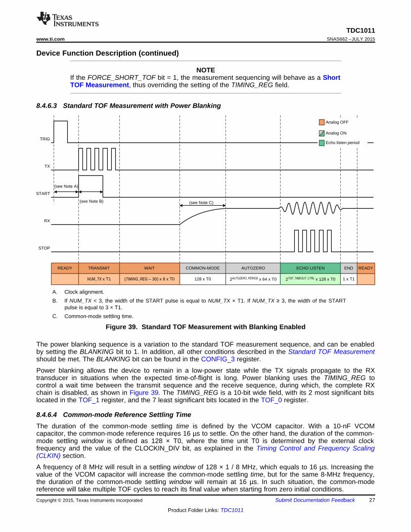
8.4.6.3 Standard TOF Measurement with Power Blanking
A. Clock alignment.B. If NUM_TX < 3, the width of the START pulse is equal to NUM_TX × T1. If NUM_TX ≥ 3, the width of the START
pulse is equal to 3 × T1.C. Common-mode settling time.
Figure 39. Standard TOF Measurement with Blanking Enabled
The power blanking sequence is a variation to the standard TOF measurement sequence, and can be enabledby setting the BLANKING bit to 1. In addition, all other conditions described in the Standard TOF Measurementshould be met. The BLANKING bit can be found in the CONFIG_3 register.
Power blanking allows the device to remain in a low-power state while the TX signals propagate to the RXtransducer in situations when the expected time-of-flight is long. Power blanking uses the TIMING_REG tocontrol a wait time between the transmit sequence and the receive sequence, during which, the complete RXchain is disabled, as shown in Figure 39. The TIMING_REG is a 10-bit wide field, with its 2 most significant bitslocated in the TOF_1 register, and the 7 least significant bits located in the TOF_0 register.
8.4.6.4 Common-mode Reference Settling TimeThe duration of the common-mode settling time is defined by the VCOM capacitor. With a 10-nF VCOMcapacitor, the common-mode reference requires 16 µs to settle. On the other hand, the duration of the common-mode settling window is defined as 128 × T0, where the time unit T0 is determined by the external clockfrequency and the value of the CLOCKIN_DIV bit, as explained in the Timing Control and Frequency Scaling(CLKIN) section.
A frequency of 8 MHz will result in a settling window of 128 × 1 / 8 MHz, which equals to 16 µs. Increasing thevalue of the VCOM capacitor will increase the common-mode settling time, but for the same 8-MHz frequency,the duration of the common-mode settling window will remain at 16 µs. In such situation, the common-modereference will take multiple TOF cycles to reach its final value when starting from zero initial conditions.Copyright © 2015, Texas Instruments Incorporated Submit Documentation Feedback 27
Product Folder Links: TDC1011

TDC1011SNAS662 –JULY 2015 www.ti.com
Device Function Description (continued)8.4.6.5 TOF Measurement IntervalThe comparators in the TDC1011's RX path can qualify and generate STOP pulses from a received echo withinan interval set by the TOF_TIMEOUT_CTRL field in the TIMEOUT register. The listening interval can beextended in the standard TOF measurement (without blanking) by a period controlled with the TIMING_REG field(see Standard TOF Measurement).
If the number of STOP events programmed in the NUM_RX field is not received within the listening interval, atimeout event will occur and the device will return to the READY state. In addition, an error will be reported to theERROR_FLAGS register and the ERRB pin will be driven low.
The echo timeout can be disabled by setting the ECHO_TIMEOUT bit to 1 in the TIMEOUT register. If the echotimeout is disabled, the device will not exit from the receive state until the expected number of STOP events setin NUM_RX occur. If the number of events does not occur, the device can be forced out of the receive state bywriting a value of 0x03 to the ERROR_FLAGS register, or by de-asserting the EN pin, or asserting the RESETpin.
NOTEWriting a logic 1 to bit [1] of the ERROR_FLAGS register clears the state machine. Writinga logic 1 to bit[0] clears the error flags.
NOTEIt is not recommended to hold the RX in an active state for intervals longer than 100ms, asthe comparator auto-zero may no longer be accurate.
8.4.7 Error ReportingThe TDC1011 will report an error when the receive signals do not match the expected configuration. The ERRBpin will go low to indicate the presence of an error condition. Reading the ERROR_FLAGS register providesinformation about the condition(s) that caused the error.
The ERR_SIG_WEAK bit indicates that the number of received and qualified zero-crossings was less than theexpected number set in the NUM_RX register field and a timeout occurred. This error is cleared when bit [0] iswritten to 1.
The ERR_NO_SIG bit indicates that no signals were received and a timeout occurred. Writing a 1 to this bitresets the state machine, halts active measurements and returns the device to SLEEP or READY mode. Thiserror is cleared when bit [0] is written to 1.
The ERR_SIG_HIGH bit indicates that the received echo amplitude exceeds the largest echo qualificationthreshold at the input of the comparators. The ERR_SIG_HIGH error is only reported when theECHO_QUAL_THDL register field is set to 7h. Writing a 1 to this bit will reset all the error flags and reset theERRB pin to high.
NOTEIt is recommended to reset the state machine when the error flags are cleared. This canbe done simultaneously by writing a value of 0x03 to the ERROR_FLAGS register.
8.5 Programming
8.5.1 Serial Peripheral Interface (SPI)The serial interface consists of serial data input (SDI), serial data output (SDO), serial interface clock (SCLK) andchip select bar (CSB). The serial interface is used to configure the TDC1011 parameters available in variousconfiguration registers. All the registers are organized into individually addressable byte-long registers with aunique address.
28 Submit Documentation Feedback Copyright © 2015, Texas Instruments Incorporated
Product Folder Links: TDC1011

c7 c6 c5 c4 c3 c2 c1 c0 d7 d6 d5 d4 d3 d2 d1
CSB
SCK
COMMAND FIELD DATA FIELD
1 2 3 4 5 6 7 8 9 10 11 12 13 14 15 16
LSBMSB
Address (6 bits) Write Data (8-bits)resvd
SDI
d7 d6 d5 d4 d3 d2 d1
Read Data (8-bits)
SDO
LSBMSB
R/W
R/W = Instruction0: Read1: WriteNote: Specifying any value other than zero in bit[7] of the command byte is prohibited.
d0
d0
TDC1011www.ti.com SNAS662 –JULY 2015
Programming (continued)The communication on the SPI bus normally supports write and read transactions. A write transaction consists ofa single write command byte, followed by single data byte. A read transaction consists of a single read commandbyte followed by 8 SCLK cycles. The write and read command bytes consist of 1 reserved bit, a 1-bit instruction,and a 6-bit register address. Figure 40 shows the SPI protocol for a transaction involving one byte of data (reador write).
Figure 40. SPI Protocol
8.5.1.1 Chip Select Bar (CSB)CSB is an active-low signal and needs to be low throughout a transaction. That is, CSB should not pulsebetween the command byte and the data byte of a single transaction.
De-asserting CSB always terminates an ongoing transaction, even if it is not yet complete. Re-asserting CSB willalways bring the device into a state ready for the next transaction, regardless of the termination status of aprevious transaction.
8.5.1.2 Serial Clock (SCLK)SCLK can idle high or low. It is recommended to keep SCLK as clean as possible to prevent glitches fromcorrupting the SPI frame.
8.5.1.3 Serial Data Input (SDI)SDI is driven by the SPI master by sending the command and the data byte to configure the AFE.
8.5.1.4 Serial Data Output (SDO)SDO is driven by the AFE when the SPI master initiates a read transaction.
Copyright © 2015, Texas Instruments Incorporated Submit Documentation Feedback 29
Product Folder Links: TDC1011

TDC1011SNAS662 –JULY 2015 www.ti.com
8.6 Register Maps
NOTE• Reserved bits must be written to 0 unless otherwise indicated.• Read-back value of reserved bits and registers is unspecified and should be discarded.• Recommended values must be programmed and forbidden values must not be
programmed where they are indicated to avoid unexpected results.
8.6.1 TDC1011 RegistersTable 3 list the memory-mapped registers for the TDC1011. All register addresses not listed in Table 3 should beconsidered as reserved locations and the register contents should not be modified.
Table 3. TDC1011 REGISTERSAddress (Hex) Acronym Register Name Reset Value Section
0h CONFIG_0 Config-0 45h See here1h CONFIG_1 Config-1 40h See here2h CONFIG_2 Config-2 0h See here3h CONFIG_3 Config-3 3h See here4h CONFIG_4 Config-4 1Fh See here5h TOF_1 TOF-1 0h See here6h TOF_0 TOF-0 0h See here7h ERROR_FLAGS Error Flags 0h See here8h TIMEOUT Timeout 19h See here9h CLOCK_RATE Clock Rate 0h See here
8.6.1.1 CONFIG_0 Register (address = 0h) [reset = 45h] (map)
Figure 41. CONFIG_0 Register
(MSB) 7 6 5 4 3 2 1 0 (LSB)TX_FREQ_DIV NUM_TX
R/W-2h R/W-5h
LEGEND: R/W = Read or write; R = Read only; R/W1C = Read or write 1 to clear
Table 4. CONFIG_0 Register Field DescriptionsBit Field Type Reset Description
Frequency divider for TX clock and T10h: Divide by 21h: Divide by 42h: Divide by 8 (default)
[7:5] TX_FREQ_DIV (1) R/W 2h 3h: Divide by 164h: Divide by 325h: Divide by 646h: Divide by 1287h: Divide by 256
Number of TX pulses in a burst, ranging from 0 to 31.[4:0] NUM_TX R/W 5h5h: 5 pulses (default)
(1) See Timing Control and Frequency Scaling (CLKIN) for the definition of the time period T1.
30 Submit Documentation Feedback Copyright © 2015, Texas Instruments Incorporated
Product Folder Links: TDC1011

TDC1011www.ti.com SNAS662 –JULY 2015
8.6.1.2 CONFIG_1 Register (address = 1h) [reset = 40h] (map)
Figure 42. CONFIG_1 Register
(MSB) 7 6 5 4 3 2 1 0 (LSB)RESERVED RESERVED NUM_RX
R/W-1h R/W-0h R/W-0h
LEGEND: R/W = Read or write; R = Read only; R/W1C = Read or write 1 to clearTable 5. CONFIG_1 Register Field Descriptions
Bit Field Type Reset Description
[7:6] RESERVED R/W 1h 1h: Reserved (default)[5:3] RESERVED R/W 0h Must always be written 0h (default)
Number of expected receive events0h: Do not count events (32 STOP pulses output) (default)1h: 1 event (1 STOP pulse output)2h: 2 events (2 STOP pulses output)
[2:0] NUM_RX R/W 0h 3h: 3 events (3 STOP pulses output)4h: 4 events (4 STOP pulses output)5h: 5 events (5 STOP pulses output)6h: 6 events (6 STOP pulses output)7h: 7 events (7 STOP pulses output)
8.6.1.3 CONFIG_2 Register (address = 2h) [reset = 0h] (map)
Figure 43. CONFIG_2 Register
(MSB) 7 6 5 4 3 2 1 0 (LSB)VCOM_SEL MEAS_MODE DAMPING RESERVED
R/W-0h R/W-0h R/W-0h R/W-0h
LEGEND: R/W = Read or write; R = Read only; R/W1C = Read or write 1 to clear
Table 6. CONFIG_2 Register Field DescriptionsBit Field Type Reset Description
Common-mode voltage reference control[7] VCOM_SEL R/W 0h 0h: Internal (default)
1h: External
AFE measurement type[6] MEAS_MODE R/W 0h 0h: Time-of-flight measurement (default)
1h: Temperature measurement
TX burst damping[5] DAMPING R/W 0h 0h: Disable damping (default)
1h: Enable damping[4:0] RESERVED R/W 0h Must always be written 0h (default)
8.6.1.4 CONFIG_3 Register (address 3h) [reset = 3h] (map)
Figure 44. CONFIG_3 Register
(MSB) 7 6 5 4 3 2 1 0 (LSB)RESERVED TEMP_MODE TEMP_RTD_SEL TEMP_CLK_DIV BLANKING ECHO_QUAL_THLD
R/W-0h R/W-0h R/W-0h R/W-0h R/W-0h R/W-3h
LEGEND: R/W = Read or write; R = Read only; R/W1C = Read or write 1 to clear
Copyright © 2015, Texas Instruments Incorporated Submit Documentation Feedback 31
Product Folder Links: TDC1011

TDC1011SNAS662 –JULY 2015 www.ti.com
Table 7. CONFIG_3 Register Field DescriptionsBit Field Type Reset Description
[7] RESERVED R/W 0h 0h: Reserved (default)
Temperature measurement channels[6] TEMP_MODE R/W 0h 0h: Measure REF, RTD1 and RTD2 (default)
1h: Measure REF and RTD1
RTD type[5] TEMP_RTD_SEL R/W 0h 0h: PT1000 (default)
1h: PT500
Clock divider for temperature mode[4] TEMP_CLK_DIV R/W 0h 0h: Divide by 8 (default)
1h: Use TX_FREQ_DIV
Power blanking in standard TOF measurements. The blankinglength is controlled with the TIMING_REG field (see StandardTOF Measurement with Power Blanking).[3] BLANKING R/W 0h0h: Disable power blanking (default)1h: Enable power blanking
Echo qualification DAC threshold level with respect to VCOM
0h: –35 mV1h: –50 mV2h: –75 mV
[2:0] ECHO_QUAL_THLD R/W 3h 3h: –125 mV (default)4h: –220 mV5h: –410 mV6h: –775 mV7h: –1500 mV
8.6.1.5 CONFIG_4 Register (address = 4h) [reset = 1Fh] (map)
Figure 45. CONFIG_4 Register
(MSB) 7 6 5 4 3 2 1 0 (LSB)RECEIVE_ TRIG_EDGE_RESERVED TX_PH_SHIFT_POSMODE POLARITY
R/W-0h R/W-0h R/W-0h R/W-1Fh
LEGEND: R/W = Read or write; R = Read only; R/W1C = Read or write 1 to clear
Table 8. CONFIG_4 Register Field DescriptionsBit Field Type Reset Description
[7] RESERVED R/W 0h 0h: Reserved (default)
Receive echo mode[6] RECEIVE_MODE R/W 0h 0h: Single echo (default)
1h: Multi echo
Trigger edge polarity[5] TRIG_EDGE_POLARITY R/W 0h 0h: Rising edge (default)
1h: Falling edge
TX 180° pulse shift position, ranging from 0 to 31.[4:0] TX_PH_SHIFT_POS R/W 1Fh 1Fh: Position 31 (default)
It is not recommended to set TX_PH_SHIFT_POS to 0 or 1.
32 Submit Documentation Feedback Copyright © 2015, Texas Instruments Incorporated
Product Folder Links: TDC1011

TDC1011www.ti.com SNAS662 –JULY 2015
8.6.1.6 TOF_1 Register (address = 5h) [reset = 0h] (map)
Figure 46. TOF_1 Register
(MSB) 7 6 5 4 3 2 1 0 (LSB)PGA_GAIN PGA_CTRL LNA_CTRL LNA_FB TIMING_REG[9:8]
R/W-0h R/W-0h R/W-0h R/W-0h R/W-0h
LEGEND: R/W = Read or write; R = Read only; R/W1C = Read or write 1 to clearTable 9. TOF_1 Register Field Descriptions
Bit Field Type Reset Description
PGA gain0h: 0 dB (default)1h: 3 dB2h: 6 dB
[7:5] PGA_GAIN R/W 0h 3h: 9 dB4h: 12 dB5h: 15 dB6h: 18 dB7h: 21 dB
PGA control[4] PGA_CTRL R/W 0h 0h: Active (default)
1h: Bypassed and powered off
LNA control[3] LNA_CTRL R/W 0h 0h: Active (default)
1h: Bypassed and powered off
LNA feedback mode[2] LNA_FB R/W 0h 0h: Capacitive feedback (default)
1h: Resistive feedback
TIMING_REG field's 2 most-significant bits (see Standard TOFMeasurement and Standard TOF Measurement with Power[1:0] TIMING_REG[9:8] R/W 0h Blanking)0h: 0 (default)
8.6.1.7 TOF_0 Register (address = 6h) [reset = 0h] (map)
Figure 47. TOF_0 Register
(MSB) 7 6 5 4 3 2 1 0 (LSB)TIMING_REG[7:0]
R/W-0h
LEGEND: R/W = Read or write; R = Read only; R/W1C = Read or write 1 to clear
Table 10. TOF_0 Register Field DescriptionsBit Field Type Reset Description
TIMING_REG field's 8 least-significant bits (see Standard TOFMeasurement and Standard TOF Measurement with Power[7:0] TIMING_REG[7:0] R/W 0h Blanking)0h: 0 (default)
Copyright © 2015, Texas Instruments Incorporated Submit Documentation Feedback 33
Product Folder Links: TDC1011

TDC1011SNAS662 –JULY 2015 www.ti.com
8.6.1.8 ERROR_FLAGS Register (address = 7h) [reset = 0h] (map)
Figure 48. ERROR_FLAGS Register
7 (MSB) 6 5 4 3 2 1 0 (LSB)ERR_ ERR_RESERVED ERR_NO_SIGSIG_WEAK SIG_HIGH
R-0h R-0h R/W1C-0 R/W1C-0
LEGEND: R/W = Read or write; R = Read only; R/W1C = Read or write 1 to clearTable 11. ERROR_FLAGS Register Field Descriptions (1) (2)
Bit Field Type Reset Description
[7:3] RESERVED R 0h 0h: Reserved (default)
1h: The number of received and qualified zero-crossings was[2] ERR_SIG_WEAK R 0h less than the expected number set in NUM_RX field and a
timeout occurred.
1h: No signals were received and timeout occurred.Writing a 1 to this field resets the state machine, halts active[1] ERR_NO_SIG R/W1C 0hmeasurements and returns the device to the SLEEP or READYmode.
1h: The received echo amplitude exceeds the largest echoqualification threshold at the input of the comparators. The error
[0] ERR_SIG_HIGH R/W1C 0h is only reported when ECHO_QUAL_THLD = 0x07.Writing a 1 to this field will reset all the error flags and reset theERRB pin to high.
(1) It is recommended to read the error status register or the ERRB pin before initiating a new measurement.(2) All error flags should be cleared before initiating a new measurement.
8.6.1.9 TIMEOUT Register (address = 8h) [reset = 19h] (map)
Figure 49. TIMEOUT Register
(MSB) 7 6 5 4 3 2 1 0 (LSB)FORCE_ ECHO_RESERVED SHORT_TOF_BLANK_PERIOD TOF_TIMEOUT_CTRLSHORT_TOF TIMEOUT
R/W-0h R/W-0h R/W-3h R/W-0h R/W-1h
LEGEND: R/W = Read or write; R = Read only; R/W1C = Read or write 1 to clear
Table 12. TIMEOUT Register Field DescriptionsBit Field Type Reset Description
[7] RESERVED R/W 0h 0h: Reserved (default)
Short time-of-flight control[6] FORCE_SHORT_TOF R/W 0h 0h: Disabled (default)
1h: Force a short time-of-flight measurement
Short time-of-flight blanking period (see Short TOFMeasurement)0h: 8 × T01h: 16 × T02h: 32 × T0
[5:3] SHORT_TOF_BLANK_PERIOD (1) R/W 3h3h: 64 × T0 (default)4h: 128 × T05h: 256 × T06h: 512 × T07h: 1024 × T0
(1) See Timing Control and Frequency Scaling (CLKIN) for the definition of the time period T0.
34 Submit Documentation Feedback Copyright © 2015, Texas Instruments Incorporated
Product Folder Links: TDC1011

TDC1011www.ti.com SNAS662 –JULY 2015
Table 12. TIMEOUT Register Field Descriptions (continued)Bit Field Type Reset Description
Echo receive timeout control (see TOF Measurement Interval)[2] ECHO_TIMEOUT R/W 0h 0h: Enable echo timeout (default)
1h: Disable timeout
Echo listening window timeout (see TOF Measurement Interval)0h: 128 × T0
[1:0] TOF_TIMEOUT_CTRL (1) R/W 1h 1h: 256 × T0 (default)2h: 512 × T03h: 1024 × T0
8.6.1.10 CLOCK_RATE Register (address = 9h) [reset = 0h] (map)
Figure 50. CLOCK_RATE Register
(MSB) 7 6 5 4 3 2 1 0 (LSB)RESERVED CLOCKIN_DIV AUTOZERO_PERIOD
R/W-0h R/W-0h R/W-0h
LEGEND: R/W = Read or write; R = Read only; R/W1C = Read or write 1 to clear
Table 13. CLOCK_RATE Register Field Descriptions (1)
Bit Field Type Reset Description
[7:3] RESERVED R/W 0h 0h: Reserved (default)
CLKIN divider to generate T0[2] CLOCKIN_DIV (1) R/W 0h 0h: Divide by 1 (default)
1h: Divide by 2
Receiver auto-zero period0h: 64 × T0 (default)
[1:0] AUTOZERO_PERIOD (1) R/W 0h 1h: 128 × T02h: 256 × T03h: 512 × T0
(1) See Timing Control and Frequency Scaling (CLKIN) for the definition of the time period T0.
Copyright © 2015, Texas Instruments Incorporated Submit Documentation Feedback 35
Product Folder Links: TDC1011

STOP
START
SP
I
EN
16-MHz CLK
RREF
TX
RX
RE
SE
T
ER
RB
OSC
RTD
Concentration
Level
TR
IGG
ER
TMS320F28035C2000 MCU
TDC1011 OR Gate
TDC1011SNAS662 –JULY 2015 www.ti.com
9 Application and Implementation
NOTEInformation in the following applications sections is not part of the TI componentspecification, and TI does not warrant its accuracy or completeness. TI’s customers areresponsible for determining suitability of components for their purposes. Customers shouldvalidate and test their design implementation to confirm system functionality.
9.1 Application InformationThe TDC1011 is an analog front-end for ultrasonic sensing applications. The device is typically used for thedriving and sensing of ultrasonic transducers to perform accurate time-of-flight measurements. Ultrasonic time-of-flight sensing allows for fluid level, fluid identification or concentration measurements.
9.2 Typical Applications
9.2.1 Level and Fluid Identification Measurements
Figure 51. Level or Concentration Measurement Application Diagram
36 Submit Documentation Feedback Copyright © 2015, Texas Instruments Incorporated
Product Folder Links: TDC1011

@ =61( × ?
2
TDC1011www.ti.com SNAS662 –JULY 2015
Typical Applications (continued)9.2.1.1 Design Requirements
Table 14. Design ParametersDESIGN PARAMETER EXAMPLE VALUE
Fluid LevelRange 2 – 10 cm
Fluid IdentificationAccuracy 0.5% concentration variationDistance 5.08 cm
9.2.1.2 Detailed Design Procedure
9.2.1.2.1 Level Measurements
For level sensing applications, the total time-of-flight (TOF) of the sound wave in the fluid is measured. Thepulses transmitted by a bottom mounted transducer travel through the fluid, to the surface of the fluid. Thediscontinuity between the fluid and air generates a reflected wave which returns back to the bottom mountedtransducer.
At the beginning of a measurement cycle, the transducer is connected to a transmit channel of the AFE, and thetransmit burst excites the transducer to generate an ultrasound wave. Synchronous to the TX burst, a STARTpulse is generated by the TDC1011 to indicate the start of a measurement. After the transmission is completed,and depending on the device configuration, the transducer is connected to a receive channel of the AFE.
When a valid echo is received, the TDC1011 generates a STOP pulse. Generation of multiple STOP pulses ispossible through register configuration of the device. The START and STOP signal times are compared todetermine the TOF.
The level of the fluid can be determined using the following equation:
where• d is the fluid level in meters (m)• TOF is the time-of-flight in seconds (s)• c is the speed of sound in the fluid in meters per second (m/s) (6)
Copyright © 2015, Texas Instruments Incorporated Submit Documentation Feedback 37
Product Folder Links: TDC1011

?IA@EQI =2 × @
61(
Trigger
START
TX
STOP
Echo Pulse received
RX
TOF
TDC1011SNAS662 –JULY 2015 www.ti.com
Figure 52. Relation Between Transmit and Receive Pulses in Level Measurements
Level measurements have 2 main criteria: resolution and range (maximum height). Resolution accuracies of 1-2mm are achievable but are impractical due to any environmental disturbances, such as tank vibrations, creatingmillimeter level surface waves. Ranges of up to 1 m are measurable utilizing VDD level excitation pulses, butsurface disturbances and signal loss over longer distances make the reliable echo reception an issue. Greaterlevel measurement reception can be achieved by mechanical means (level guide tube) and/or electronic means(level shifting the TX pulses to greater voltages; see TIDA-00322).
9.2.1.2.2 Fluid Identification
The TDC1011 can be used to measure the time-of-flight for a known distance to calculate the speed of sound(cmedium) in the fluid. This application utilizes the same circuitry as the level example but a transducer in a sidemounted configuration transmitting across the container or to a target at a known distance from the transducer.
The temperature can also be measured to compensate for the temperature variation of sound. With the knowndistance, TOF and temperature, the speed of sound in the fluid can be determined and the identity of themedium verified.
After measuring the time-of-flight for the fixed distance, the speed of sound can be calculated as follows:
where• cmedium is the speed of sound in the fluid in meters per second (m/s)• d is the level in meters (m)• TOF is the time of flight in seconds (s) (7)
38 Submit Documentation Feedback Copyright © 2015, Texas Instruments Incorporated
Product Folder Links: TDC1011

Spe
ed o
f sou
nd in
med
ium
(m
/s)
1400
1425
1450
1475
1500
1525
1550
1575
1600
1625
1650
Distille
d W
ater
Tap W
ater
DEF 10.
0%
DEF 20.
0%
DEF 30.
0%
DEF 31.
5%
DEF 32.
0%
DEF 32.
5%Height (cm)
Tim
e-of
-flig
ht (P
s)
2 3 4 5 6 7 8 9 1030
45
60
75
90
105
120
135
150
TDC1011www.ti.com SNAS662 –JULY 2015
The measurement process is identical to the level example above. The speed of sound can be used to uniquelyidentify a variety of fluids. In this example, the concentration of diesel exhaust fluid (DEF) is measured with adesired accuracy resolution of 0.5% of concentration variation. For most fluids, the speed of sound varies overtemperature, so every application will be different. In this example, all samples were all at ambient temperature of23°C.
9.2.1.3 Application CurvesThe data used in the following level and fluid identification graphs was collected using an ultrasonic test cell. Thetest cell is an acrylic plastic container with width of 2.54 cm and ultrasonic transducers attached to the outsideusing cyanoacrylate glue. The transducers in this experiment were STEMiNC 1MHz piezo electric ceramic discs(SMD10T2R111). Equivalent transducers with the following characteristics could be used:• Piezo material: SM111• Dimensions: 10mm diameter x 2mm thickness• Resonant frequency: 1050 kHz (thickness mode)
Fluid Height in Tank Time-of-Flight (µs)Full (10 cm) 145
Fluid Speed of sound (m/s)Full – 1 (9 cm) 131Distilled water 1481.87Full – 2 (8 cm) 118
Tap water 1483.133 cm 50DEF 10.0% 1530.492 cm 35DEF 20.0% 1576.42DEF 30.0% 1620.00Figure 53. Time-of-Flight for Fluid Height in TankDEF 31.5% 1627.37DEF 32.0% 1629.15DEF 32.5% 1630.00
Figure 54. Speed of Sound for Various Fluids and DieselExhaust Fluid (DEF) Concentration
Copyright © 2015, Texas Instruments Incorporated Submit Documentation Feedback 39
Product Folder Links: TDC1011

Spe
ed o
f sou
nd in
med
ium
(m
/s)
1481.0
1481.5
1482.0
1482.5
1483.0
1483.5
Distille
d W
ater
Tap W
ater
Spe
ed o
f sou
nd in
med
ium
(m
/s)
1618
1620
1622
1624
1626
1628
1630
1632
DEF 30.
0%
DEF 31.
5%
DEF 32.
0%
DEF 32.
5%
TDC1011SNAS662 –JULY 2015 www.ti.com
Fluid Speed of sound (m/s)Fluid Speed of sound (m/s) DEF 30.0% 1620.00
Distilled water 1481.87 DEF 31.5% 1627.37Tap water 1483.13 DEF 32.0% 1629.15
DEF 32.5% 1630.00Figure 55. Speed of Sound in Distilled Water and TapWater
Figure 56. Speed of Sound of Various Diesel Exhaust Fluid(DEF) Concentrations
40 Submit Documentation Feedback Copyright © 2015, Texas Instruments Incorporated
Product Folder Links: TDC1011

TDC1011www.ti.com SNAS662 –JULY 2015
10 Power Supply RecommendationsThe analog circuitry of the TDC1011 is designed to operate from an input voltage supply range between 2.7Vand 5.5V. It is recommended to place a 100nF ceramic bypass capacitor to ground as close as possible to theVDD pins. In addition, an electrolytic or tantalum capacitor with value greater than 1µF is recommended. Thebulk capacitor does not need to be in close vicinity with the TDC1011 and could be close to the voltage sourceterminals or at the output of the voltage regulators powering the TDC1011.
The IO circuitry of the TDC1011 is designed to operate from an input voltage supply range between 1.8V and5.5V. The IO voltage supply (VIO) can be lower than the analog voltage supply (VDD), but it should not exceed it.It is also recommended to place a 100nF ceramic bypass capacitor to ground as close as possible to the VIOpin. If a separate source or regulator is used for VIO, an additional electrolytic or tantalum capacitor with valuegreater than 1µF is recommended.
In some cases an additional 10µF bypass capacitor may further reduce the supply noise.
Copyright © 2015, Texas Instruments Incorporated Submit Documentation Feedback 41
Product Folder Links: TDC1011

NC
RX
VCOM
PGAIN
PGAOUT
TX
NC
GND
CLKIN
COMPIN
RTD1RTD2
VIO
SDO
RREF
RES
ERRB
SDI
CSB
SCLK
START
STOP
LNAOUT
RESET
TRIGGER
EN
VDD
VDD
TD
C1011
Matched trace
length to stopwatch
/MCU
MCUSPI Master
VIA to Ground Plane
VIA to Bottom or Internal Layer
Top Layer
Bottom Layer
1
System Clock
To RTDs: Match trace length (resistance)
RTD1
RTD2MCU I/Os
Trigger:stopwatch/MCU
MCU I/Os
GN
D
GND
GND
GND
GND
GND
TDC1011SNAS662 –JULY 2015 www.ti.com
11 Layout
11.1 Layout Guidelines• In a 4-layer board design, the recommended layer stack order from top to bottom is: signal, ground, power
and signal.• Bypass capacitors should be placed in close proximity to the VDD and VIO pins.• The length of the START and STOP traces from the DUT to the stopwatch/MCU should be matched to
prevent uneven signal delays. Also, avoid unnecessary via-holes on these traces and keep the routing asshort/direct as possible to minimize parasitic capacitance on the PCB.
• Match the length (or resistance) of the traces leading to the RTD sensors. PCB series resistance will beadded in series to the RTD sensors.
• Route the SPI signal traces close together. Place a series resistor at the source of SDO (close to the DUT)and series resistors at the sources of SDI, SCLK and CSB (close to the master MCU).
11.2 Layout Example
Figure 57. TDC1011 Board Layout (Capacitive Feedback Mode)
42 Submit Documentation Feedback Copyright © 2015, Texas Instruments Incorporated
Product Folder Links: TDC1011

TDC1011www.ti.com SNAS662 –JULY 2015
12 Device and Documentation Support
12.1 Device Support
12.1.1 Third-Party Products DisclaimerTI'S PUBLICATION OF INFORMATION REGARDING THIRD-PARTY PRODUCTS OR SERVICES DOES NOTCONSTITUTE AN ENDORSEMENT REGARDING THE SUITABILITY OF SUCH PRODUCTS OR SERVICESOR A WARRANTY, REPRESENTATION OR ENDORSEMENT OF SUCH PRODUCTS OR SERVICES, EITHERALONE OR IN COMBINATION WITH ANY TI PRODUCT OR SERVICE.
12.1.2 Development SupportFor development support see the following:• Automotive Ultrasonic Fluid Level/Quality Measurement Reference Design, TIDA-00322
12.2 Community ResourcesThe following links connect to TI community resources. Linked contents are provided "AS IS" by the respectivecontributors. They do not constitute TI specifications and do not necessarily reflect TI's views; see TI's Terms ofUse.
TI E2E™ Online Community TI's Engineer-to-Engineer (E2E) Community. Created to foster collaborationamong engineers. At e2e.ti.com, you can ask questions, share knowledge, explore ideas and helpsolve problems with fellow engineers.
Design Support TI's Design Support Quickly find helpful E2E forums along with design support tools andcontact information for technical support.
12.3 TrademarksE2E is a trademark of Texas Instruments.
12.4 Electrostatic Discharge CautionThese devices have limited built-in ESD protection. The leads should be shorted together or the device placed in conductive foamduring storage or handling to prevent electrostatic damage to the MOS gates.
12.5 GlossarySLYZ022 — TI Glossary.
This glossary lists and explains terms, acronyms, and definitions.
13 Mechanical, Packaging, and Orderable InformationThe following pages include mechanical, packaging, and orderable information. This information is the mostcurrent data available for the designated devices. This data is subject to change without notice and revision ofthis document. For browser-based versions of this data sheet, refer to the left-hand navigation.
Copyright © 2015, Texas Instruments Incorporated Submit Documentation Feedback 43
Product Folder Links: TDC1011

PACKAGE OPTION ADDENDUM
www.ti.com 12-Jul-2015
Addendum-Page 1
PACKAGING INFORMATION
Orderable Device Status(1)
Package Type PackageDrawing
Pins PackageQty
Eco Plan(2)
Lead/Ball Finish(6)
MSL Peak Temp(3)
Op Temp (°C) Device Marking(4/5)
Samples
TDC1011PW ACTIVE TSSOP PW 28 48 Green (RoHS& no Sb/Br)
CU SN Level-1-260C-UNLIM -40 to 125 TDC1011PW
TDC1011PWR ACTIVE TSSOP PW 28 2500 Green (RoHS& no Sb/Br)
CU SN Level-1-260C-UNLIM -40 to 125 TDC1011PW
(1) The marketing status values are defined as follows:ACTIVE: Product device recommended for new designs.LIFEBUY: TI has announced that the device will be discontinued, and a lifetime-buy period is in effect.NRND: Not recommended for new designs. Device is in production to support existing customers, but TI does not recommend using this part in a new design.PREVIEW: Device has been announced but is not in production. Samples may or may not be available.OBSOLETE: TI has discontinued the production of the device.
(2) Eco Plan - The planned eco-friendly classification: Pb-Free (RoHS), Pb-Free (RoHS Exempt), or Green (RoHS & no Sb/Br) - please check http://www.ti.com/productcontent for the latest availabilityinformation and additional product content details.TBD: The Pb-Free/Green conversion plan has not been defined.Pb-Free (RoHS): TI's terms "Lead-Free" or "Pb-Free" mean semiconductor products that are compatible with the current RoHS requirements for all 6 substances, including the requirement thatlead not exceed 0.1% by weight in homogeneous materials. Where designed to be soldered at high temperatures, TI Pb-Free products are suitable for use in specified lead-free processes.Pb-Free (RoHS Exempt): This component has a RoHS exemption for either 1) lead-based flip-chip solder bumps used between the die and package, or 2) lead-based die adhesive used betweenthe die and leadframe. The component is otherwise considered Pb-Free (RoHS compatible) as defined above.Green (RoHS & no Sb/Br): TI defines "Green" to mean Pb-Free (RoHS compatible), and free of Bromine (Br) and Antimony (Sb) based flame retardants (Br or Sb do not exceed 0.1% by weightin homogeneous material)
(3) MSL, Peak Temp. - The Moisture Sensitivity Level rating according to the JEDEC industry standard classifications, and peak solder temperature.
(4) There may be additional marking, which relates to the logo, the lot trace code information, or the environmental category on the device.
(5) Multiple Device Markings will be inside parentheses. Only one Device Marking contained in parentheses and separated by a "~" will appear on a device. If a line is indented then it is a continuationof the previous line and the two combined represent the entire Device Marking for that device.
(6) Lead/Ball Finish - Orderable Devices may have multiple material finish options. Finish options are separated by a vertical ruled line. Lead/Ball Finish values may wrap to two lines if the finishvalue exceeds the maximum column width.
Important Information and Disclaimer:The information provided on this page represents TI's knowledge and belief as of the date that it is provided. TI bases its knowledge and belief on informationprovided by third parties, and makes no representation or warranty as to the accuracy of such information. Efforts are underway to better integrate information from third parties. TI has taken andcontinues to take reasonable steps to provide representative and accurate information but may not have conducted destructive testing or chemical analysis on incoming materials and chemicals.TI and TI suppliers consider certain information to be proprietary, and thus CAS numbers and other limited information may not be available for release.

PACKAGE OPTION ADDENDUM
www.ti.com 12-Jul-2015
Addendum-Page 2
In no event shall TI's liability arising out of such information exceed the total purchase price of the TI part(s) at issue in this document sold by TI to Customer on an annual basis.
OTHER QUALIFIED VERSIONS OF TDC1011 :
• Automotive: TDC1011-Q1
NOTE: Qualified Version Definitions:
• Automotive - Q100 devices qualified for high-reliability automotive applications targeting zero defects

TAPE AND REEL INFORMATION
*All dimensions are nominal
Device PackageType
PackageDrawing
Pins SPQ ReelDiameter
(mm)
ReelWidth
W1 (mm)
A0(mm)
B0(mm)
K0(mm)
P1(mm)
W(mm)
Pin1Quadrant
TDC1011PWR TSSOP PW 28 2500 330.0 16.4 6.8 10.2 1.6 8.0 16.0 Q1
PACKAGE MATERIALS INFORMATION
www.ti.com 11-Jul-2015
Pack Materials-Page 1
*All dimensions are nominal
Device Package Type Package Drawing Pins SPQ Length (mm) Width (mm) Height (mm)
TDC1011PWR TSSOP PW 28 2500 367.0 367.0 35.0
PACKAGE MATERIALS INFORMATION
www.ti.com 11-Jul-2015
Pack Materials-Page 2


IMPORTANT NOTICE
Texas Instruments Incorporated and its subsidiaries (TI) reserve the right to make corrections, enhancements, improvements and otherchanges to its semiconductor products and services per JESD46, latest issue, and to discontinue any product or service per JESD48, latestissue. Buyers should obtain the latest relevant information before placing orders and should verify that such information is current andcomplete. All semiconductor products (also referred to herein as “components”) are sold subject to TI’s terms and conditions of salesupplied at the time of order acknowledgment.TI warrants performance of its components to the specifications applicable at the time of sale, in accordance with the warranty in TI’s termsand conditions of sale of semiconductor products. Testing and other quality control techniques are used to the extent TI deems necessaryto support this warranty. Except where mandated by applicable law, testing of all parameters of each component is not necessarilyperformed.TI assumes no liability for applications assistance or the design of Buyers’ products. Buyers are responsible for their products andapplications using TI components. To minimize the risks associated with Buyers’ products and applications, Buyers should provideadequate design and operating safeguards.TI does not warrant or represent that any license, either express or implied, is granted under any patent right, copyright, mask work right, orother intellectual property right relating to any combination, machine, or process in which TI components or services are used. Informationpublished by TI regarding third-party products or services does not constitute a license to use such products or services or a warranty orendorsement thereof. Use of such information may require a license from a third party under the patents or other intellectual property of thethird party, or a license from TI under the patents or other intellectual property of TI.Reproduction of significant portions of TI information in TI data books or data sheets is permissible only if reproduction is without alterationand is accompanied by all associated warranties, conditions, limitations, and notices. TI is not responsible or liable for such altereddocumentation. Information of third parties may be subject to additional restrictions.Resale of TI components or services with statements different from or beyond the parameters stated by TI for that component or servicevoids all express and any implied warranties for the associated TI component or service and is an unfair and deceptive business practice.TI is not responsible or liable for any such statements.Buyer acknowledges and agrees that it is solely responsible for compliance with all legal, regulatory and safety-related requirementsconcerning its products, and any use of TI components in its applications, notwithstanding any applications-related information or supportthat may be provided by TI. Buyer represents and agrees that it has all the necessary expertise to create and implement safeguards whichanticipate dangerous consequences of failures, monitor failures and their consequences, lessen the likelihood of failures that might causeharm and take appropriate remedial actions. Buyer will fully indemnify TI and its representatives against any damages arising out of the useof any TI components in safety-critical applications.In some cases, TI components may be promoted specifically to facilitate safety-related applications. With such components, TI’s goal is tohelp enable customers to design and create their own end-product solutions that meet applicable functional safety standards andrequirements. Nonetheless, such components are subject to these terms.No TI components are authorized for use in FDA Class III (or similar life-critical medical equipment) unless authorized officers of the partieshave executed a special agreement specifically governing such use.Only those TI components which TI has specifically designated as military grade or “enhanced plastic” are designed and intended for use inmilitary/aerospace applications or environments. Buyer acknowledges and agrees that any military or aerospace use of TI componentswhich have not been so designated is solely at the Buyer's risk, and that Buyer is solely responsible for compliance with all legal andregulatory requirements in connection with such use.TI has specifically designated certain components as meeting ISO/TS16949 requirements, mainly for automotive use. In any case of use ofnon-designated products, TI will not be responsible for any failure to meet ISO/TS16949.
Products ApplicationsAudio www.ti.com/audio Automotive and Transportation www.ti.com/automotiveAmplifiers amplifier.ti.com Communications and Telecom www.ti.com/communicationsData Converters dataconverter.ti.com Computers and Peripherals www.ti.com/computersDLP® Products www.dlp.com Consumer Electronics www.ti.com/consumer-appsDSP dsp.ti.com Energy and Lighting www.ti.com/energyClocks and Timers www.ti.com/clocks Industrial www.ti.com/industrialInterface interface.ti.com Medical www.ti.com/medicalLogic logic.ti.com Security www.ti.com/securityPower Mgmt power.ti.com Space, Avionics and Defense www.ti.com/space-avionics-defenseMicrocontrollers microcontroller.ti.com Video and Imaging www.ti.com/videoRFID www.ti-rfid.comOMAP Applications Processors www.ti.com/omap TI E2E Community e2e.ti.comWireless Connectivity www.ti.com/wirelessconnectivity
Mailing Address: Texas Instruments, Post Office Box 655303, Dallas, Texas 75265Copyright © 2015, Texas Instruments Incorporated