tdttp2500p100 user guide v0
TRANSCRIPT

November 16, 2017 © 2017 Transphorm Inc. Subject to change without notice. evk009.0 1
User Guide
TDTTP2500P100: 2.5kW Bridgeless Totem-pole PFC Evaluation Board
Overview This user guide describes the TDTTP2500P100_0v1 2.5kW bridgeless totem-pole power factor correction (PFC) evaluation board. Very high efficiency single-phase AC-DC conversion is achieved with the TPH3212PS, a diode-free Gallium Nitride (GaN) FET bridge with low reverse-recovery charge. Using GaN FETs in the fast-switching leg of the circuit and low-resistance MOSFETs in the slow-switching leg of the circuit results in improved performance and efficiency. For more information and complete design files, please visit transphormusa.com/tp25kit. The TDTTP2500P100_0v1-KIT is for evaluation purposes only.
Figure 1. TDTTP2500P100_0v1 2.5kW totem-pole PFC evaluation board
Warning
This evaluation board is intended to demonstrate GaN FET technology and is for demonstration purposes only and no guarantees are made for standards compliance.
There are areas of this evaluation board that have exposed access to hazardous high voltage levels. Exercise caution to avoid contact with those voltages. Also note that the evaluation board may retain high voltage temporarily after input power has been removed. Exercise caution when handling.
When testing converters on an evaluation board, ensure adequate cooling. Apply cooling air with a fan blowing across the converter or across a heatsink attached to the converter. Monitor the converter temperature to ensure it does not exceed the maximum rated per the datasheet specification.
TDTTP2500P100_0v1 November 16, 2017 evk009.0 2
TDTTP2500P100 User Guide
The TDTTP2500P100-KIT includes:
• TDTTP2500P100 totem-pole PFC assembly
• Texas Instruments F28335 control card
• 12VDC auxiliary power adaptor
Complete design files and support documentation can be found online at transphormusa.com/tp25kit.
TDTTP2500P100 input/output specifications • Input voltage: 85VAC to 265VAC, 47Hz to 63Hz• Input current: 18ARMS; 1250W at 115VAC, 2500W at 230VAC
• 10% overload short time: 11ARMS; 1250W at 115VAC, 2500W at 230VAC
• Ambient temperature: <50ºC• Output voltage: 390VDC ± 5VDC
• PWM frequency: 100kHz• Auxiliary supply: 12VDC for bias voltage• Power dissipation in the GaN FET: Limited by the maximum junction temperature; refer to the TPH3212PS datasheet
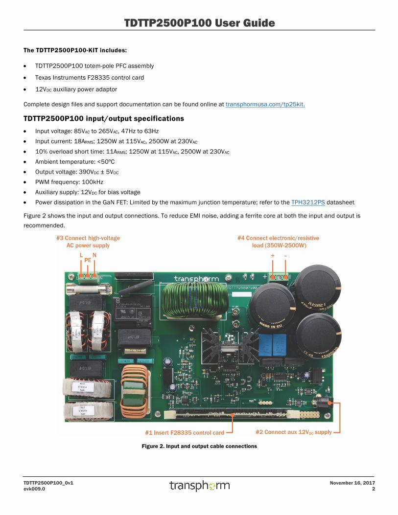
Figure 2 shows the input and output connections. To reduce EMI noise, adding a ferrite core at both the input and output is recommended.
Figure 2. Input and output cable connections

TDTTP2500P100_0v1 November 16, 2017 evk009.0 3
TDTTP2500P100 User Guide
Circuit description The bridgeless totem-pole PFC topology is shown in Figure 3. Two GaN FETs and two low-resistance silicon (Si) MOSFETs are used to eliminate diode drops and improve efficiency. Further information and discussion on the performance and the characteristics of the bridgeless PFC circuit is provided in [1].
Figure 3. Bridgeless totem-pole PFC boost converter based on low-resistance MOSFETs for line rectification
Figure 4(a) is a simplified schematic of a totem-pole PFC in continuous conduction mode (CCM) mode, focused on minimizing conduction losses. It comprises two fast-switching GaN FETs (Q1 and Q2) operating at a high pulse-width-modulation (PWM) frequency and two very low-resistance MOSFETs (S1 and S2) operating at a much slower line frequency (50Hz/60Hz). The primary current path includes one fast switch and one slow switch only, with no diode drop. The function of S1 and S2 is that of a synchronized rectifier as illustrated in Figures 4(b) and 4(c). During the positive AC cycle, S1 is on and S2 is off, forcing the AC neutral line tied to the negative terminal to the DC output. The opposite applies for the negative cycle.
(a) (b) (c)
Figure 4. Totem-pole PFC with GaN FETs (a) simplified schematic, (b) during positive AC cycle and (c) during negative AC cycle
In either AC polarity, the two GaN FETs form a synchronized boost converter with one transistor acting as a master switch to allow energy intake by the boost inductor (LB), and another transistor as a slave switch to release energy to the DC output. The roles of the two GaN devices interchange when the polarity of the AC input changes; therefore, each transistor must be able to perform both master and slave functions. To avoid shoot-through a dead time is built in between two switching events, during which both transistors are momentarily off. To allow CCM operation, the body diode of the slave transistor must function as a flyback diode for the inductor current to flow during dead time. The diode current; however, must quickly reduce to zero and transition to the reverse blocking state once the master switch turns on.
This is the critical process for a totem-pole PFC which, with the high QRR of the body diode of high-voltage Si MOSFETs, results in abnormal spikes, instability, and associated high switching losses. The low QRR of the GaN switches allows designers to overcome this barrier.
Q2
VAC
Q1
+
–VD
SD2
SD1
iL
VS
VIN
N
LB
VS
S2
S1
VO+
VO–
Q2
Q1VIN
N
LB
VS
S2
S1
VO+
VO–
Q2
Q1VIN
N
LB
VS
S2
S1
VO+
VO–
Q2
Q1

TDTTP2500P100_0v1 November 16, 2017 evk009.0 4
TDTTP2500P100 User Guide
As seen in Figure 5, inductive tests at 400V bus show healthy voltage waveforms up to inductor current exceeding 27A using either a high-side (Figure 5(a)) or low-side (Figure 5(b)) GaN transistor as a master switch. With a design goal of 2.5kW output power in CCM mode at 230VAC input, the required inductor current is 12A. This test confirms a successful totem-pole power block with enough current overhead.
(a) High side (b) Low side
Figure 5. Waveforms of two hard-switched GaN FETs when setting (a) high-side as a master and (b) low-side as a master
One issue inherent in the bridgeless totem-pole PFC is the operation mode transition at AC voltage zero-crossing. For instance, when the circuit operation mode changes from positive half-line to negative half-line at the zero-crossing, the duty ratio of the high-side GaN switch changes abruptly from almost 100% to 0% and the duty ratio of low-side GaN switch changes from 0% to 100%. Due to the slow reverse recovery of diodes (or body diode of a MOSFET), the voltage VD cannot jump from ground to VDC instantly; a current spike will be induced. To avoid the problem, a soft-start at every zero-crossing is implemented to gently reverse duty ratio (a soft-start time of a few switching cycles is enough). The TDTTP2500P100 evaluation board is designed to run in CCM and the larger inductance alleviates the current spike issue at zero-crossing.
Dead time control The required form of the gate-drive signals is shown in Figure 5. The times marked A are the dead times when neither transistor is driven on. The dead time must be greater than zero to avoid shoot-through currents. The Si8230 gate drive chip ensures a minimum dead time based on the value of resistor R24, connected to the DT input. The dead time in ns is equal to the resistance in kΩ x 10, so the default value of 12k corresponds to 120ns. This will add to any dead time already present in the input signals. The on-board pulse generator circuit; for example, creates dead times of about 60ns (see Figure 6). The resulting dead time at the gate pins of Q1 and Q2 is about 100ns. Either shorting or removing R24 will reduce the dead time to 60ns.
Figure 6. Non-overlapping gate pulses

TDTTP2500P100_0v1 November 16, 2017 evk009.0 5
TDTTP2500P100 User Guide
While a typical Si MOSFET has a maximum dV/dt rating of 50V/ns, the TPH3212PS GaN FET will switch at dV/dt of 100V/ns or higher to achieve the lowest possible switching loss. At this level of operation, even the layout becomes a significant contributor to performance. As shown in Figure 8, the recommended layout keeps a minimum gate drive loop and keeps the traces between the switching nodes very short--with the shortest practical return trace to the power bus and ground. The power ground plane provides a large cross-sectional area to achieve an even ground potential throughout the circuit. The layout carefully separates the power ground and the IC (small signal) ground, only joining them at the source pin of the FET to avoid any possible ground loop.
Note that the Transphorm GaN FETs in TO-220 packages have pinout configuration of G-S-D, instead of the traditional G-D-S of a MOSFET. The G-S-D configuration is designed with thorough consideration to minimize the gate source driving loop, reducing parasitic inductance and to separate the driving loop (gate source) and power loop (drain source) to minimize noise. All PCB layers of the TDTTP2500P100 design are shown Figure 8(a-c) and available in the design files.
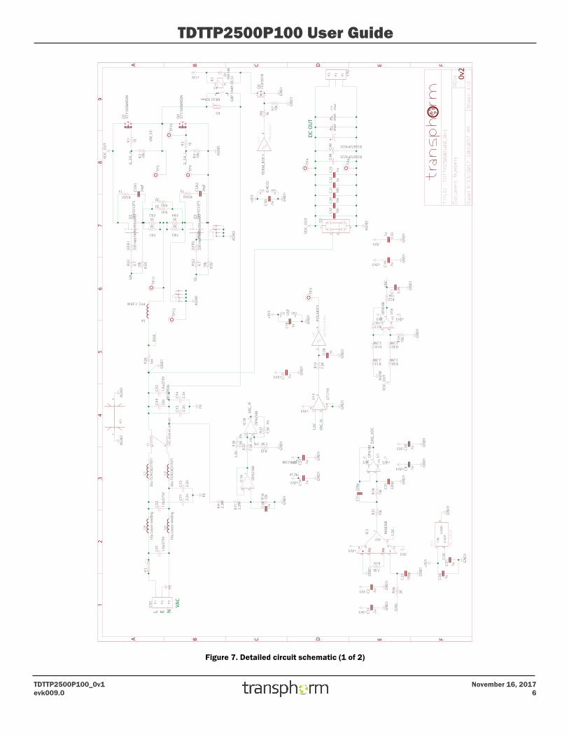
Design details A detailed circuit schematic is shown in Figures 7 and 8, the PCB layers in Figure 9, and the parts list in Table 1 (also included in the design files).
TDTTP2500P100_0v1 November 16, 2017 evk009.0 6
TDTTP2500P100 User Guide
Figure 7. Detailed circuit schematic (1 of 2)

TDTTP2500P100_0v1 November 16, 2017 evk009.0 7
TDTTP2500P100 User Guide
Figure 8. Detailed circuit schematic (2 of 2)

TDTTP2500P100_0v1 November 16, 2017 evk009.0 8
TDTTP2500P100 User Guide
Table 1. TDTTP2500P100 evaluation board bill of materials (BOM)
Designator Qty Value Descriptor/Package Manufacturer Part Number
Manufacturer
HS1 1 529802B02500G 530002B02500G Aavid Thermalloy D3, D4 2 DIODE-DO-214AC ES1J Micro Commercial CN1, CN2 2 FCI_20020316-3P 20020316-H031B01LF FCI D2 1 GBJ2506 GBJ2506-BP Micro Commercial SV2 1 MA04-1 961104-6404-AR 3M SV1 1 MA07-2 67996-114HLF FCI J1 1 PJ-002AH PJ-002AH CUI F1 1 SH32 01020078H Littelfuse TP7, TP8 2 TEKTRONIX-PCB 131-4353-00 Tektronix TP1, TP2, TP3, TP4, TP5, TP6, TP9, TP10, TP11, TP12, TP14
11 TESTPOINT-KEYSTONE5015
5015 Keystone
C2, C5, C8, C9, C16, C17, C18, C19, C24, C27, C30, C31, C32, C33, C35, C37, C39, C42, C44, C50, C52, C53, C54, C55, C56, C58
26 0.1µF C-EUC0603 CC0603KRX7R8BB104 Yageo
C22, C23 2 0.1µF C-EUC1812 C1812V104KDRACTU Kemet CX1, CX2, CX3 3 1µF/275V ECQ-U2A474ML1.0U ECQ-U2A105ML Panasonic R1, R3 2 10Ω R-US_R0603 RNCP0603FTD10R0 Stackpole R40 1 10Ω R-US_R1206 ERJ-8ENF10R0V Panasonic R26, R33 2 100kΩ R-US_R0805 RJ-6ENF1003V Panasonic C25 1 100pF C-EUC0603 06035A101FAT2A AVX Corporation C7, C12, C29 3 100µF/25V CPOL-USE2.5-7 ESK107M025AC3AA Kemet R2, R4, R7, R8, R10, R15, R34, R37, R39
9 10kΩ R-US_R0603 ESR03EZPJ103 ROHM Semiconductor
C20, C21, C47 3 10nF C-EUC1206 C3216C0G2J822J160AA TDK C3, C4, C6, C10, C38 5 10µF C-EUC1206 CL31A106KAHNNNE Samsung Electro-Mechanics L4, L5 2 10µF loose
winding DM-TOROID P1192_1 MPS Industries
R24 1 12kΩ R-US_R0805 RC0805FR-0712KL Yageo RSN1, RSN2 2 15Ω R-US_R1206 RNCP1206FTD15R0 Stackpole R16, R17, R18, R21, R31, R32
6 15kΩ R-US_R0805 05FR-0715KL Yageo
R20 1 165kΩ R-US_R0805 ERJ-6ENF1653V Panasonic D1 1 DIODE-SOD123 1N4148W-E3-18 Vishay R6 1 1kΩ R-US_R0805 RC0805JR-071KL Yageo C26, C28 2 1nF C-EUC0805 CC0805KRX7R9BB102 Yageo C45, C57, C69 3 1µF C-EUC0805 CC0805ZRY5V8BB105 Yageo C63, C64, C65, C66 4 1µF C-USC0603 TMK107B7105KA-T Taiyo Yuden R9, R11, R12, R14, R29, R30
6 2.2MΩ R-US_R1210 KTR25JZPF2204 ROHM Semiconductor
CY1, CY2, CY3, CY4 4 2.2nF PHE850YCAP PHE850EA4220MA01R17 Kemet C59 1 2.2µF C-EUC1206 CL31B225KAHNNNE Samsung Electro-Mechanics R41, R42 2 20Ω R-US_R1206 RNCP1206FTD20R0 Stackpole C11, C51 2 220pF C-EUC0805 CC0805KRX7R9BB221 Yageo CX4 1 22nF ECQ-U2A474ML22N PME271M522MR30 Kemet C40, C41 2 22µF C-EUC1206 CL31A226KAHNNNE Samsung Electro-Mechanics CSN1, CSN2 2 47pF C-EUC1206 CL31C470JIFNFNE Samsung Electro-Mechanics R38, R46 2 2kΩ R-US_R0805 ERJ-6ENF2001V Panasonic C1 1 3.3nF C-EUC0805 C0805C332K5RACTU Kemet FB1, FB2, FB3, FB4 4 30Ω R-US_R0805 BLM21SN300SH1D Murata GFB1, GFB2 2 330Ω R-US_R0603 MPZ1608S331ATA00 TDK RG1, RG2 2 4.7Ω R-US_R0603 ESR03EZPJ4R7 ROHM Semiconductor R22, R23 2 4.7Ω R-US_R1206 CRM1206-JW-4R7ELF Bourns

TDTTP2500P100_0v1 November 16, 2017 evk009.0 9
TDTTP2500P100 User Guide
Designator Qty Value Descriptor/Package Manufacturer Part Number
Manufacturer
C34, C36, C43, C46 4 4.7µF C-EUC1206 C0805C475K4PACTU Kemet C72, C73, C74 3 470µF ELE_CAP_D35MM_P10
MM ALC10A471DF450 Kemet
L1, L2 2 DM-TOROID77071 P1139 rev A. MPS Industries R28 1 5mΩ R-US_0613/15 12FR005E Ohmite R19, R13 2 7.5kΩ 0.1% R-US_R0805 RC0805FR-077K5L Yageo R25, R27, R35, R36 4 7.5kΩ 0.1% R-US_R0805 ERA-6AEB752V Panasonic IC4 1 74AUC1G17DBV SN74LVC1G17DBVR Texas Instruments CM1, CM5 2 ACM4520 ACM4520-142-2P-T000 TDK C48, C49 2 B32672P4225 B32672P4225K Epcos (TDK) L3 1 CMC_BOURNS_8119_
RC 8121-RC Bourns
CN3 1 DIMM socket 5390213-1 TE Connectivity Q5 1 BSS138-7-F FDV301N Fairchild/ON Semiconductor K1 1 JTN1AS-PA-F-DC12V JTN1AS-PA-F-DC12V Omron Electronics IC2 1 INA826R INA826AID Texas Instruments IC3 1 ISL21010 ISL21010CFH315Z-TK Intersil U14 1 LT1719 LT1719CS6#TRMPBF Linear Technology U8 1 MAX1735 MAX1735EUK50+T Maxim Integrated R5 1 10Ω THERMISTOR-
AMETHERM SL32 10015 Ametherm
U5 1 NC7SZ14M5X NC7SZ14M5X Fairchild/ON Semiconductor U1, U16 2 AD8031RJ OPA188AIDBVT Texas Instruments IC1 1 AD826R OPA2188AIDR Texas Instruments U11 1 PDS1-S5-S12-M-TR PDS1-S5-S12-M-TR CUI L6 1 P1941_A P1941_A MPS Industries U7 1 SI8230 SI8230BB-D-IS1 Silicon Labs U6 1 SI8233 SI8233BB-D-IS1 Silicon Labs Q1, Q4 2 STY105NM50N STY105NM50N STMicroelectronics Q2, Q3 2 TPH3212PS TPH3212PS Transphorm U10 1 TPS60403 TPS60403DBVR Texas Instruments U2 1 TPS73033 TPS73033DBVR Texas Instruments U3 1 V7805-500 7805-500 CUI 7 Stand off (nylon 1/2) 1902C Keystone 7 Machine screw (ss 1/2) 9902 Keystone 1 Thermal pad for Q3 4169G Aavid Thermalloy 1 Screw for FETs HS 9902 Keystone 2 Washer shoulder to be
placed between screw and FET assembly
3049 Keystone
1 Nut for FETs to HS 9600 Keystone 1 Control card TMDSCNCD28335 Texas Instruments 1 12Vdc aux supply SWI10-12-N-P5 CUI
For the TDTTP2500P100 evaluation board, the PFC circuit has been implemented on a 4-layer PCB. The GaN FET half-bridge is built with Transphorm’s TPH3212PS (72mΩ) GaN FET. The slow Si switches are STY105NM50N (22mΩ) superjunction MOSFETs. The inductor is made of a High Flux core with an inductance of 480µH and a DC resistance of 25mΩ and designed to operate at 100kHz. A simple 0.5A rated high/low side driver IC (Si8230) with 0/12V as on/off states directly drives each GaN FET. A 150MHz DSP (TMS320F28335) handles the control algorithm. The voltage and current loop controls are similar to a conventional boost PFC converter. The feedback signals are DC output voltage (VO), AC input potentials (VACP and VACN) and inductor current (IL). The input voltage polarity and RMS value are determined from VACP and VACN. The outer voltage loop output multiplied by |VAC| gives a sinusoidal current reference. The current loop gives the proper duty ratio for the boost circuit. The polarity determines how PWM signal is distributed to drive Q1 and Q2. A soft-start sequence with a duty ratio ramp is employed for a short period at each AC zero-crossing for better stability.

TDTTP2500P100_0v1 November 16, 2017 evk009.0 10
TDTTP2500P100 User Guide
(a) PCB top layer
(b) PCB bottom layer

TDTTP2500P100_0v1 November 16, 2017 evk009.0 11
TDTTP2500P100 User Guide
(c) PCB inner layer 2 (ground plane) + inner layer 3 (power plane)
Figure 9. PCB layers
Using the board The TDTTP2500P100 board can be used for evaluating Transphorm GaN FETs in a bridgeless totem-pole PFC circuit and is building block but not a complete circuit.
Powering on the board
1. Insert the control card
• LED1 ON indicates DSP power is on • LED2 BLINKING indicates the DSP is running • LED3 ON indicates the DSP has stopped running due to fault protection (over voltage or current)
2. Connect an electronic/resistive load to the corresponding marking (CN2). The requirements for the resistive load are
• At 115VAC input: 350W to ≤1250W • At 230VAC input: 350W to ≤2500W
3. Connect the 12VDC auxiliary supply (included) to the evaluation board 4. With high-voltage power off, connect the high-voltage AC power input to the corresponding marking (CN1) on the PCB; N and
L (PE: potential ground) 5. Turn on the AC power input (85VAC to 265VAC, 50Hz to 60Hz); minimum power load for turn-on sequence is 350W 6. Monitor CN2 output voltage with VDC meter to verify that 390V ±5V is generated 7. Electronic/resistive load can be increased while AC supply is on and board is functional

TDTTP2500P100_0v1 November 16, 2017 evk009.0 12
TDTTP2500P100 User Guide
Powering off the board
1. Switch off the high-voltage AC power input 2. Power off DC bias
Operational waveforms Figure 10 shows the converter start-up procedure: DC input current (CH1), DC bus voltage waveform (CH2), and voltage waveform of the fast leg switching node (CH3). For the start up, there are three phases to charge the DC bus to a reference voltage.
1. In the beginning the relay K1 is open and DC bus capacitors are charged by input voltage through NTC and diode bridge 2. When the VDC is over 100V, K1 is closed to bypass the NTC and the VDC increases to the peak of the input voltage 3. After 100ms, the leg of the GaN FET is engaged in voltage closed-loop control and the DC bus voltage reference slowly
increases to the rated voltage 385V
The NTC and diode bridge are applied in this circuit to avoid high inrush current flow through the GaN FETs.
Figure 10. Start-up of the bridgeless totem-pole PFC CH1: VG, CH2: iL, CH3: VO, CH4: VD
Figure 11. Active switch version of the bridgeless totem-pole PFC at low line, full load
CH1: PWM gate signal for SD2, CH2: iL waveform (10A/div), CH3: VD waveform (100V/div), CH4: AC input polarity signal
Figure 12. Waveform of VDS of Q2 at iL=20A CH1: IIN=10A/div, CH2: VDS=100V/div

TDTTP2500P100_0v1 November 16, 2017 evk009.0 13
TDTTP2500P100 User Guide
Figure 13 shows the transition between two half-cycles. In Figure 13(a) the AC line enters the negative half and soft-start gradually increases voltage VD from 0V to 385V, and in Figure 13(b), VD decreases from 385V to 0V.
(a)
(b)
Figure 13. Zero-crossing transitional waveforms (a) from negative to positive half-cycle and (b) from positive to negative half-cycle CH1: PW<gate signal for SD2, CH2: iL, CH3: VD
Probing As shown in Figure 14, on the evaluation board there are two probing sockets for measuring VGS and VDS of low side GaN FET and MOSFET.
Probing tips: Low side GaN FET VGS and VDS
Passive voltage probes
Figure 14. VGS and VDS of low side GaN FET measurement socket tips and current measurement position
Efficiency sweep and EMI For the efficiency measurement, the input/output voltage and current will be measured for the input/output power calculation with a power analyzer. Efficiency has been measured at 120VAC or 230VAC input and 390VDC ±5V output using the WT1800 precision power analyzer from Yokogawa. The efficiency and power loss results for the TDTTP2500P100 are shown in Figure 15. The extremely high efficiency of 98.9% at 230VAC input, and 97.5% at 115VAC input is the highest among PFC designs with similar PWM frequency, enabling customers to reach peak system efficiency that meets or exceeds the 80 PLUS standard.

TDTTP2500P100_0v1 November 16, 2017 evk009.0 14
TDTTP2500P100 User Guide
Figure 15. TDTTP2500P100 efficiency results
Conducted emissions have also been measured for this board using an LIN-115A LISN by Com-Power. The results compared to EN55022A limits are shown in Figure 16. Note that the EMI test was done by using the lab-use power supply for an auxiliary 12V source. Do not use wall AC-DC adaptor for the EMI test.
Figure 16. Conducted emissions @ 115V, 680W
Maximum load limit The TDTTP2500P100 evaluation board can run overload in a short time. The rated input current for <230VAC input is 11A and the 10% overload current can be 12A. The input over-current protection (OCP) will be triggered when the current is over 12A.

TDTTP2500P100_0v1 November 16, 2017 evk009.0 15
TDTTP2500P100 User Guide
Warnings The TDTTP2500P100 is for evaluation purposes only and is not intended to be a finished product and does not include all protection features found in commercial power supplies. Additional warnings to keep in mind:
1. An isolated AC source should be used as input. An isolated lab bench-grade power supply or the included AUX DC supply should also be used for the 12V DC power supply. Float the oscilloscope by using an isolated oscilloscope or by disabling the PE (Protective Earth) pin in the power plug. Float the current probe power supply (if any) by disabling the PE pin in the power plug.
2. Use a resistive load only. The totem-pole PFC kit can work at zero load with burst mode and the output voltage will be swinging between 375V and 385V during burst mode.
3. The evaluation board is not fully-tested at large load steps. DO NOT apply a very large step in the load (>1000W) when it is running.
4. DO NOT manually probe the waveforms when the board is running. Set up probing before powering up the demo board. 5. The auxiliary VDC supply must be 12V. The evaluation board will not work under 10V or over 15V VDC, for example. 6. DO NOT touch any part of the evaluation board when it is running. 7. When plugging the control cards into the socket, make sure the control cards are fully pushed down with a clicking sound. 8. If the evaluation circuit goes into protection mode it will work as a diode bridge by shutting down all PWM functions. Recycle
the bias power supply to reset the DSP and exit protection mode. 9. DO NOT use a passive probe to measure control circuit signals and power circuit signals at the same time. GND1 and AGND
are not the same ground. 10. To get clean VGS of the low side GaN FET, it is not recommended to measure the VDS at the same time. 11. It is not recommended to use a passive voltage probe for VDS and VGS measurements while simultaneously using a
differential voltage probe for VIN measurements, unless the differential probe has very good dV/dt immunity.
References
[1] Z. Liang, U. Mishra and Y. Wu, "True Bridge-less Totem-pole PFC based on GaN FETs," in PCIM, Europe, pp. 1017-1022, May 2013.

Mouser Electronics
Authorized Distributor
Click to View Pricing, Inventory, Delivery & Lifecycle Information: Transphorm:
TDTTP2500P100-KIT