technical note 1965-30
TRANSCRIPT
3PY DIVISION-
Technical Note
A Noise Rejection Filter for Waveguide
Carrying High Power
oU A
Prepared under Electronic Systems Division Contract AF 19(628)-5167 by
Lincoln Laboratory MASSACHUSETTS INSTITUTE OF TECHNOLOGY
Lexington, Massachusetts
470 LIST
1965-30
W. J. Getsinger
3 August 196!>
A ft
The work reported in this document was performed at Lincoln Laboratory, a center for research operated by Massachusetts Institute of Technology, with the support of the U.S. Air Force under Contract AF 19(628>5167.
MASSACHUSETTS INSTITUTE OF TECHNOLOGY
LINCOLN LABORATORY
A NOISE REJECTION FILTER
FOR WAVEGUIDE CARRYING HIGH POWER
W. J. GETSINGER
Group 46
TECHNICAL NOTE 1965-30
3 AUGUST 1965
TS4
LEXINGTON MASSACHUSETTS
ABSTRACT
A novel design for a waveguide band-rejection filter
carrying high power in its pass band is presented. The
resonant cavities of the filter are mounted in pairs on the
narrow walls of the guide and coupled to the guide through
rectangular openings the full height of the guide. Thus
there are no edges or radii on which electric field concen-
trations can occur. An X-band model having six cavity pairs
had a rejection greater than 80 db over k^> Mcps in its 6top
band with an insertion loss under 0.05 db and VSWR under
1.02 in its pass band. With water cooling, the filter
carried over 300 lew CW without breakdown.
Accepted for the Air Force Stanley J. Wisniewslci Lt Colonel, USAF Chief, Lincoln Laboratory Office
ii
A NOISE REJECTION FILTER FOR WAVEGUIDE CARRYING HIGH POWER
I. INTRODUCTION
The M.I.T. Lincoln Laboratory Haystack Facility transmits 100 kw CW at
7750 Mcps while receiving at 8350 Mcps using the same antenna. A reject filter
is used to reduce substantially the part of the transmitter noise that lies
within the receiver pass band and couples into the receiver. This filter is
placed in the transmitter waveguide between the generator and the diplexing
arrangement. It strongly attenuates energy around the receive frequency while
passing energy at the transmit frequency with very little attenuation or re-
flection.
Filters placed in very high power lines are typically of the absorbing,
rather than reflecting, type in order to avoid large electric fields that might
induce voltage breakdown in the structure and to provide a load in which the
undesired energy can be dissipated. However, for Haystack it was decided to
use a reflecting-type filter for the following reasons:
1. The resonators used would be timed to the receive frequency and
thus would allow only small voltages at the transmit frequency.
2. The novel design proposed had no edges or radii on which electric
field intensification could occur.
3. A terminated high-power circulator located at the generator was
available to absorb reflected energy.
k-. A reflection filter could be made to have higher stop-band loss
and lower pass-band loss than an absorption filter.
5. A reflection filter could be made smaller in volume and weight
than an absorption filter.
6. The performance of a reflection filter is more accurately pre-
dictable than is the performance of an absorption filter.
A reflecting noise-rejection filter development program was begun that re-
sulted in an interim filter design having a rejection band about 8050 Mcps and
the final filter design with a rejection band about 835O Mcps.
II. DESCRIPTION
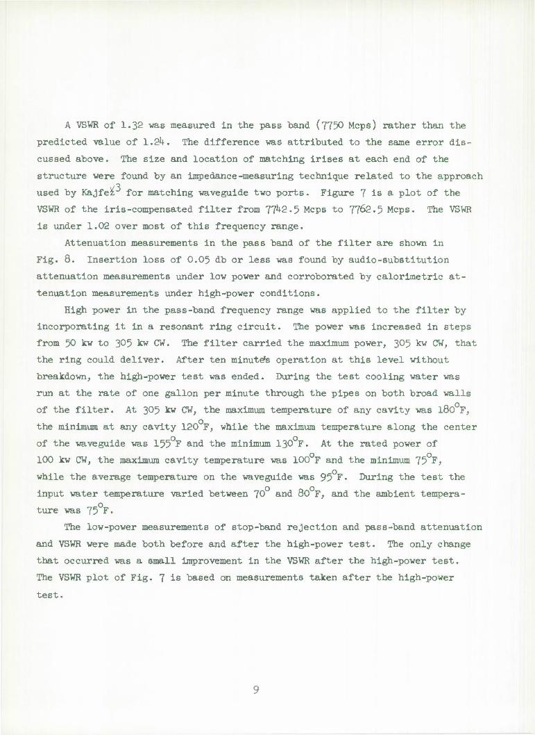
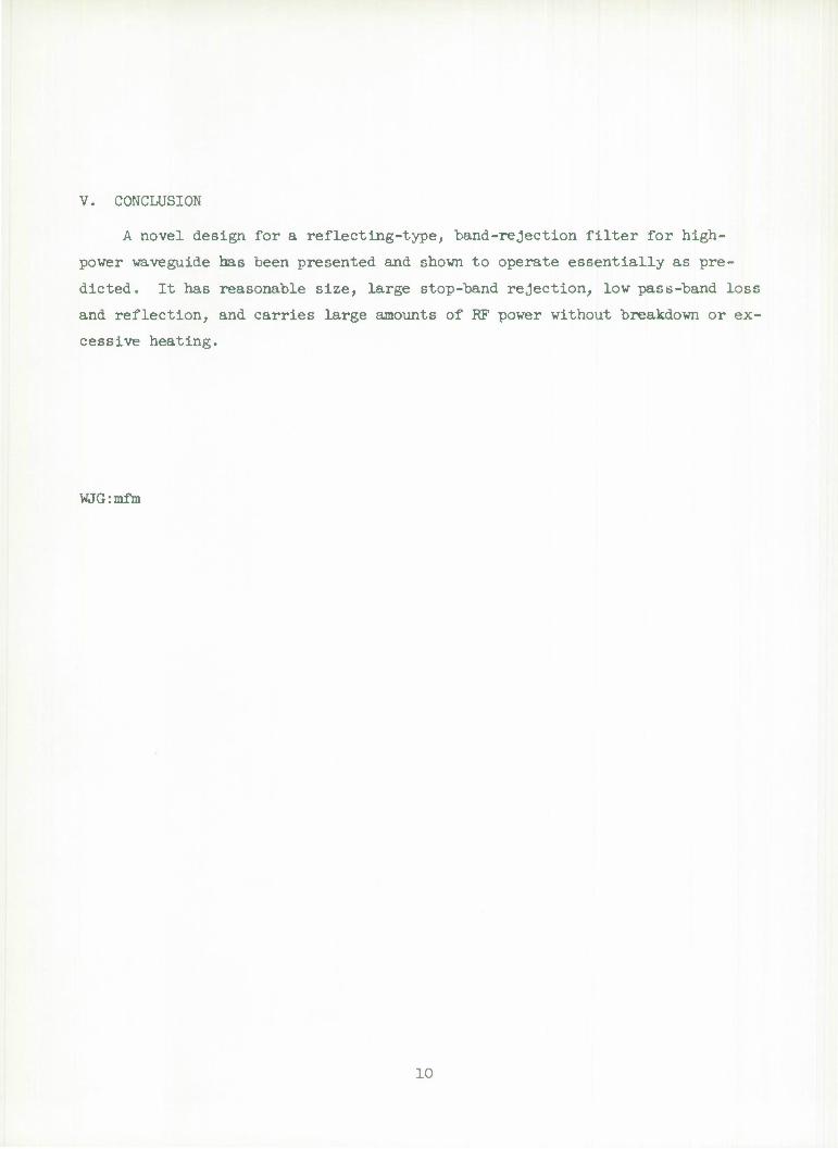
Figures l(a) and (b) show the noise-reject filters for 8050 and 835O Mcps.
The 805O Mcps filter has three pairs of resonators while the 835O Mcps filter
has six pairs, since it was required to have a wider stop band than the 805O
Mcps filter.
The waveguide size is WR-137 with inside dimensions of 0.622 x 1.372
inches. The flanges are stainless steel CPR-137F» which are preferable to
standard UG-3M*- flanges for high-power work. The pipes soldered to the broad
walls of the filters are for the cooling water needed at high power levels.
The resonators are coupled to the waveguide through openings in the narrow
wall of the waveguide. These openings run the full height of the guide so that
upper and lower walls of the waveguide and resonators are flush and continuous,
with no edges or protrusions that might cause electric field concentrations.
If the resonators had been placed on the broad walls of the waveguide, as is
usually done with reject filters, the edge of the opening between resonator
and waveguide would have been in the region of greatest electric field intensi-
ty. The electric field would be further intensified along this edge, enhancing
voltage breakdown.
The higher-order modes generated by resonators on the narrow walls of the
guide are not greatly attenuated with distance along the guide because the cut-
off frequencies of these modes are determined by the wide dimension of the
guide. In contrast, the cutoff frequencies of higher-order modes generated by
resonators mounted in the broad walls of the guide are determined by the narrow
dimension of the guide and so are more strongly attenuated with distance. In
any case, these higher-order modes provide undesired alternative coupling paths
between adjacent resonators, broadening the stop bandwidth and reducing the
maximum attenuation. Thus it is desired to suppress higher-order modes as much
as possible.
The least attenuated higher-order mode for the reject filters shown in
Figs. 1(a) and (b) is the TE?Q mode. To prevent this mode from affecting
filter performance, it was found necessary to place identical resonators iden-
tically tuned on either side of the waveguide at the same terminal plane. The
symmetry of this arrangement prevents generation of the TEp0 mode.
The next least-attenuated mode is the TE_Q mode. In order to avoid adja-
cent cavity coupling by this mode, it was found necessary to space the resonators
by five quarters of a guide wavelength rather than the usual three quarters.
Small inductive irises can be seen Just within the flanges of the two filters.
These irises match out the residual reflection of the filter to give a very low
VSWR in the pass band.
The large screws shown extending from the cavities are for fine tuning.
They allow each pair of resonators to be set to the proper resonant frequency
and to be put in electrical balance. No attempt to adjust these screws should
be made in the field.
III. DESIGN PROCEDURE
The following specifications were assigned to the 835O Mcps noise-reject
filter.
Waveguide WR-I37
Rejection 60 db min over 835O + 15 Mcps
Pass-band loss 0.1 db max at 775O Mcps
Pass-band VSWR < 1.15
Power handling 100 lew CW min
Operating temperature 60 - 150 F
Simple calculations showed that the allowed temperature variation could change
the center frequency of the filter by almost 7 Mcps. The 60 db rejection band-
width was increased to allow for this variation and 3 Mcps more were added to
allow for tuning tolerance. Thus a 60 db rejection bandwidth of UO Mcps was
used in the design of the filter.
Figure 4.03-1+ of Ref. 1 showed that a 0.01 db ripple Tchebyscheff filter
of six resonators would provide 63 db rejection over a kO Mcps band at 8350
Mcps, and that this filter would have a total stop bandwidth of 128 Mcps.
This relatively narrow stop bandwidth (l.5#) insured that the pass band
was well removed from the lossy range near the stop-band edge and allowed use
of the approximate design procedure for filters with very narrow stop band6
described in Chapter 12 of Ref. 1.
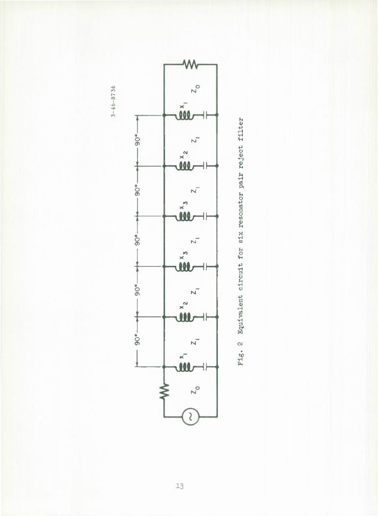
The equivalent circuit for the filter is shown in Fig. 2. All the reso-
nators are tuned to the stop-band center frequency. It might be observed that
the resonators are shown in the equivalent circuit as series-resonant circuits
shunting the transmission line, although the actual resonators are anti-
resonant structures attached to the side of the waveguide. This is not incon-
sistent because the effect is the same—open circuiting the waveguide at its
side is the same as short circuiting it at the center, when viewed from some
distance along the guide. In fact, as closely as it was practical to measure,
it was found that the axial centerline of the cavity coincided with the termi-
nal plane of the effective short circuit caused by the cavity at its resonant
frequency. This is in basic agreement with the electromagnetic boundary-value
solution for a similar structure given in Sec. 6.6 of Ref. 2. The structure of
Ref. 2 is an iris-coupled H-plane T junction. It differs from the structure
used in the filter in that it has a side arm on only one side of the main guide
and because it uses very thin irises. Also, it is based on small apertures and
does not apply near the second mode cutoff frequency, where the filter operates.
These differences make the circuit of Ref. 2 only qualitatively useful in de-
termining resonator and coupling iris sizes.
The low-pass prototype and procedure of Ref. 1 were used with the perti-
nent values given above to find the slope parameters for the resonators. Only
three slope parameters are required because the structure is symmetrical about
its center. The required slope parameters, normalized to the guide character-
istic impedance, are
xL = 87.65,
^ = 45.65,
x = 40.5O.
These slope parameters are defined on a frequency, rather than reciprocal guide
wavelength basis. The theoretical design calls for the characteristic impe-
dance, Z,, of the waveguide between resonators to be slightly less than the
generator and load impedances, Z . In the interests of mechanical simplicity,
such an impedance step was not incorporated in the actual structure. This
omission causes negligible effect in the stop band and a slightly larger maxi-
mum reflection than predicted in the pass band. However, pass-band performance
was not expected to agree with simple theory because the resonator spacing of
5A guide wavelengths at the stop-band center frequency was a poor approxima-
tion in the pass band to the frequency independent 90 line lengths assumed by
the theory. For this reason it was necessary to use small Irises at the ends
of the filter to obtain low VSWR in the pass band.
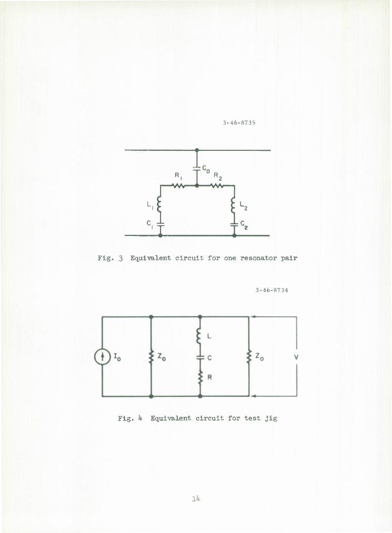
The simple resonators shown in Fig. 2 are good approximations to the ac-
tual situation in a narrow band around their resonant frequencies, but only
when both cavities of a pair are identical. A more accurate equivalent circuit
that allows for small differences between the cavities of a pair is shown in
Fig. 3« It can be seen that if the elements of subscript 1 are identical to
those of subscript 2, the circuit of Fig. 3 reduces to that of a single series
resonator. However, if any differences exist between element values of sub-
scripts 1 and 2, then the circuit has two impedance zeros separated by a pole.
The mutual capacitance C is needed to account for the fact that the two
zeros do not converge to the same frequency as one resonator of the pair is
tuned toward the frequency of the other but remain rather widely separated.
Frequency differences of about 150 to 400 Mcps, increasing with decreasing
slope parameter, were observed for the cavity pairs investigated for the filters
described herein. Electrical balance of the two resonators occurs when the
lower-frequency zero combines with the pole and both disappear. If the fre-
quencies of the zeros are observed by monitoring transmission loss of a swept
signal, the lower frequency zero will disappear only if R, = Rpj otherwise,
the transmission loss at the lower frequency will simply pass through a minimum.
It is possible to use this phenomenon to determine when a pair of cavities
is electrically balanced. Also, it is important to know where the secondary
frequencies are, since they may lie at a pass-band frequency of interest and
cause a loss peak there.
If the cavities are nearly the same and tuned nearly alike, it can be
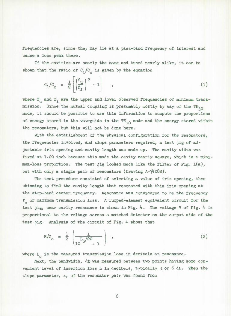
shown that the ratio of C./C is given by the equation
Cl/Co - I if \2
te1 -1 (i)
where f and f. are the upper and lower observed frequencies of minimum trans-
mission. Since the mutual coupling is presumably mostly by way of the TE_Q
mode, it should be possible to use this information to compute the proportions
of energy stored in the waveguide in the TE_0 mode and the energy stored within
the resonators, but this will not be done here.
With the establishment of the physical configuration for the resonators,
the frequencies involved, and slope parameters required, a test Jig of ad-
justable iris opening and cavity length was made up. The cavity width was
fixed at 1.00 inch because this made the cavity nearly square, which is a mini-
mum-loss proportion. The test Jig looked much like the filter of Fig. l(a),
but with only a single pair of resonators (Drawing A-7^082).
The test procedure consisted of selecting a value of iris opening, then
shimming to find the cavity length that resonated with this iris opening at
the stop-band center frequency. Resonance was considered to be the frequency
f of maximum transmission loss. A lumped-element equivalent circuit for the
test Jig, near cavity resonance is shown in Fig. k. The voltage V of Fig. h is
proportional to the voltage across a matched detector on the output side of the
test Jig. Analysis of the circuit of Fig. 1* shows that
(2) R/Zo " I L /20 \ioo/ -1 /
where L is the measured transmission loss in decibels at resonance, o
Next, the bandwidth, Af, was measured between two points having some con-
venient level of insertion loss L in decibels, typically 3 or 6 db. Then the
slope parameter, x, of the resonator pair was found from
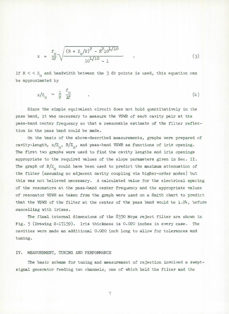
(R + Z /2) - R 10 2 _ p2inL/10
o
10 JW (3)
If R < < Z and bandwidth between the 3 <lb points is used, this equation can
be approximated by
*fh "Is • <k)
Since the simple equivalent circuit does not hold quantitatively in the
pass band, it was necessary to measure the VSWR of each cavity pair at the
pass-band center frequency so that a reasonable estimate of the filter reflec-
tion in the pass band could be made.
On the basis of the above-described measurements, graphs were prepared of
cavity-length, x/Z , R/Z , and pass-band VSWR as functions of iris opening.
The first two graphs were used to find the cavity lengths and iris openings
appropriate to the required values of the slope parameters given in Sec. II.
The graph of R/z could have been used to predict the maximum attenuation of
the filter (assuming no adjacent cavity coupling via higher-order modes) but
this was not believed necessary. A calculated value for the electrical spacing
of the resonators at the pass-band center frequency and the appropriate values
of resonator VSWR as taken from the graph were used on a Smith chart to predict
that the VSWR of the filter at the center of the pass band would be 1.24, before
cancelling with irises.
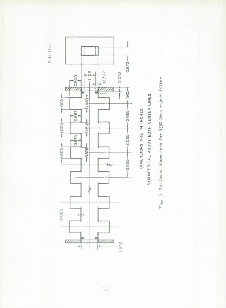
The final internal dimensions of the 835O Mcps reject filter are shown in
Fig. 5 (Drawing S-17159). Iris thickness is 0.020 inches in every case. The
cavities were made an additional 0.020 inch long to allow for tolerances and
tuning.
IV. MEASUREMENT, TUNING AND PERFORMANCE
The basic scheme for tuning and measurement of rejection involved a swept-
signal generator feeding two channels, one of which held the filter and the
other of which allowed the insertion of calibrated attenuation up to 90 db.
Essential to the operation of this technique was a low-noise TWT amplifier used
Just before detection. This amplifier allowed sufficient sensitivity to make
accurate measurements in the stop band and acted as its own limiter when over-
loaded by the much stronger signal in the pass band. The limiting action was
needed to prevent blocking and disabling the detector and following circuitry.
The tuning procedure began with all resonators detuned by the tuning
screws. The first pair of resonators was tuned for maximum attenuation at the
stop-band center frequency, 8350 Mcps. Subsequent pairs of resonators were
brought in to the same frequency, with the requirement that the stop band remain
centered on 835O Mcps after tuning. Then the screws of each pair were adjusted
the same amount but in opposite sense to reduce secondary resonances in the pass
band without changing the frequency of maximum rejection. Finally, tuning for
each resonator pair was touched up to minimize any discernible ripple across the
stop band.
The cut-off of the tuned filter was very sharp. When the oscilloscope was
adjusted to show both the pass-band response and the zero-signal base line, the
transition between pass and stop bands appeared as an almost vertical line.
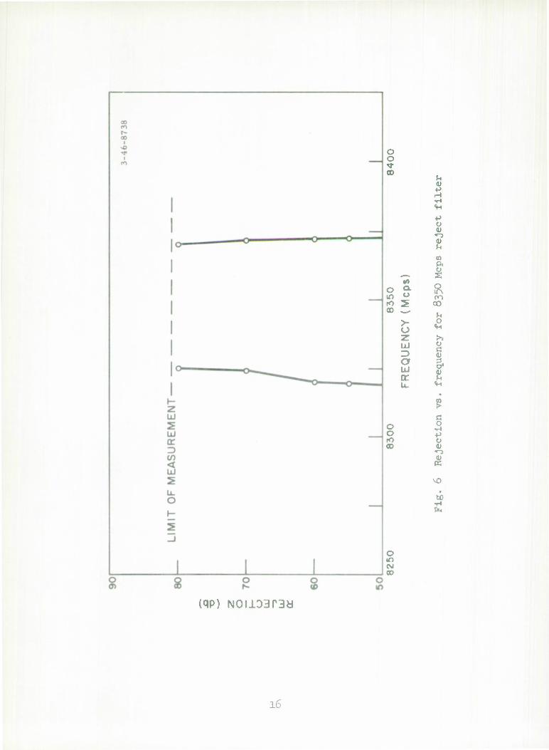
Figure 6 is a plot of the attenuation between 55 and 80 db as a function of
frequency. The slight step between 60 and 70 db on the lower-frequency side
is caused by measurement error, not by the filter.
It can be seen that the 60-db bandwidth is about 52 Mcps, rather than the
predicted value of k-0 Mcps. With the clearer vision of hindsight, the cause of
this discrepancy was traced to an erroneous measurement or test-Jig fault for
the test iris of largest opening. The displacement of this end point on the
graph of x/Z vs. iris opening was interpreted as curvature rather than error.
The result was that the four center cavity pairs have larger iris openings than
they should for the proposed design. It had been demonstrated previously with
the 805O Mcps reject filter that the design technique gave good agreement with
theory, and so no appreciable discrepancy was considered likely on that count. .
Since the error was in the preferred direction, no attempt was made to re-
work the filter.
8
A VSWR of 1.32 was measured in the pass band (7750 Mcps) rather than the
predicted value of 1.2^. The difference was attributed to the same error dis-
cussed above. The size and location of matching irises at each end of the
structure were found by an impedance-measuring technique related to the approach
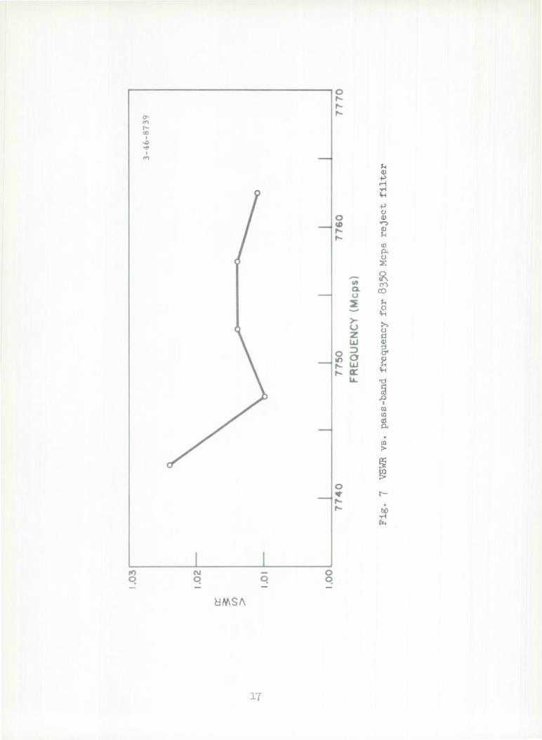
used by Kajfez for matching waveguide two ports. Figure 7 Is & plot of the
VSWR of the iris-compensated filter from 77^2.5 Mcps to 7762.5 Mcps. The VSWR
is under 1.02 over most of this frequency range.
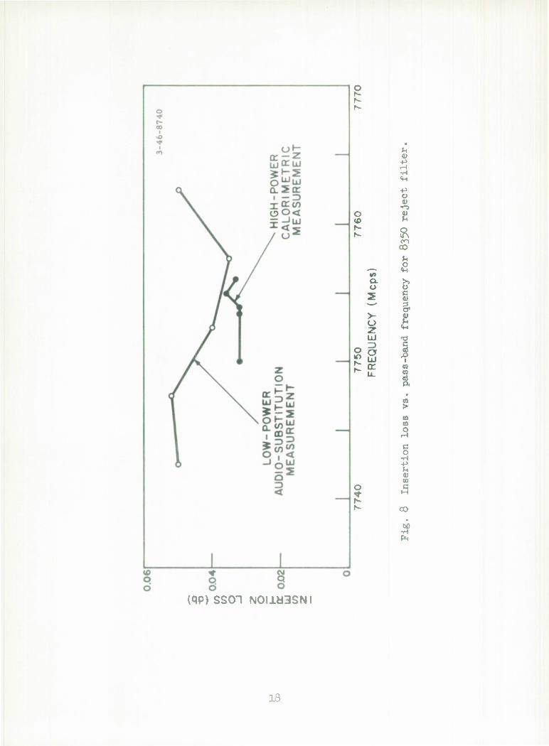
Attenuation measurements in the pass band of the filter are shown in
Fig. 8. Insertion loss of 0.05 db or less was found by audio-substitution
attenuation measurements under low power and corroborated by calorimetric at-
tenuation measurements under high-power conditions.
High power in the pass-band frequency range was applied to the filter by
incorporating it in a resonant ring circuit. The power was increased in steps
from 50 kw to 305 lew CW. The filter carried the maximum power, 305 kw CW, that
the ring could deliver. After ten minute's operation at this level without
breakdown, the high-power test was ended. During the test cooling water was
run at the rate of one gallon per minute through the pipes on both broad walls
of the filter. At 305 kw CW, the maximum temperature of any cavity was 180 F,
the minimum at any cavity 120 F, while the maximum temperature along the center
of the waveguide was 155 F and the minimum 130 F. At the rated power of
100 kw CW, the maximum cavity temperature was 100 F and the minimum 75 F,
while the average temperature on the waveguide was 95 F. During the test the
input water temperature varied between 70 and 80 F, and the ambient tempera-
ture was 75 F.
The low-power measurements of stop-band rejection and pass-band attenuation
and VSWR were made both before and after the high-power test. The only change
that occurred was a small improvement in the VSWR after the high-power test.
The VSWR plot of Fig. 7 is based on measurements taken after the high-power
test.
V. CONCLUSION
A novel design for a reflecting-type, band-rejection filter for high-
power waveguide has been presented and shown to operate essentially as pre-
dicted. It has reasonable size, large stop-band rejection, low pass-band loss
and reflection, and carries large amounts of KF power without breakdown or ex-
cessive heating.
WJG:mfm
10
P10.29-1582
I
Fig. 1 (a) Three cavity pair 8O5O Mcps reject filter
11
-r o 00
CM
I s
00
u
CO
DO
12
.0 -t
M
CO
^MrHI
M
(O
TÜÜLrHI
M
IO
-JÄlrHH
N
Owl
—JÜLHH"
(SI
^JWLHi
a; .-i •H
o D »"3
fa
O
I O w
ß X •H CD
u o
3 Ü u
w
•H En
13
3-46-8735
ic.
•^w • 2
Fig. 3 Equivalent circuit for one resonator pair
3-46-8734
Fig. h Equivalent circuit for test Jig
Ik
-f r- 00
i vO -r
i
D o o_ o I
CO -in-». o m
o o
CVJ Cd CD ö
±1 T CM CO +^>
UJ o z 0)
"•"8 _) B
(0 ac III UJ m
I Z
ft ü
^ UJ u £
z X oo ~ t- CO
UJ rr
o CD o
< t- <H
c/> z o
O CD <
CO Ö o •H
CO
z UJ
_) <
(0 a
1 n or •d
i- -p UJ c 3= s 2 >- CO £
PL.
•H
15
o o CO
10
o °- in o
CO .
>- o z UJ
a a:
o ID CM CO
•p o a;
ft o 2
& CO
U o
o a
c o o o •p fO Ü oo d)
£ vo
bO
(qp) N0i±03r3a
16
u V
B Iß ft
ft OO CO
o
>> o
I TJ
I
•H
UMSA
17
o
o iß
Ml Q- O
UJ
o
u
o
R on
CO
o
2 c B
»**•» 0 O4
>- B u z
U
UJ -Ö 3 s
2 O aS I
to to
&
to
!
to
CO
i
(qp) SSCH NOI1M3SNI
10
REFERENCES
1. G. L. Matthaei, L. Young, and E.M.T. Jones, Microwave Filters,
Impedance-Matching Networks, and Coupling Structures, (McGraw-Hill
Book Company, New York, 196*0
2. N. Marcuvitz, Ed., Waveguide Handbook, Rad. Lab. Series 10, (McGraw-
Hill Book Company, New York, 1951)-
3. D. Kajfez, "Wide-Band Matching of Lossless Waveguide Two-Ports,"
IRE Trans, on Microwave Theory and Techniques, MTT-10, l~fk (May,
1962)
19

DISTRIBUTION
W. J. Getsinger (6)
L. W. Bowles
F. J. Dominick
C. E. Muehe
W. A. Andrews
M. L. Stone
S. S. Cupoli
C. W. Jones
E. P. McCurley
J. S. Arthur
L. Rainville
A. F. Standing
R. R. Silva
20
UNCLASSIFIED Security Classification
DOCUMENT CONTROL DATA - R&D (Security classification of title, body of abstract and indexing annotation must be entered when the overall report is classified)
1. ORIGINATING ACTIVITY (Corporate author)
Lincoln Laboratory, M.I.T.
2fl. REPORT SECURITY CLASSIFICATION Unclassified
2b. GROUP None
3. REPORT TITLE
A Noise Rejection Filter for Waveguide Carrying High Power
DESCRIPTIVE NOTES (Type of report and inclusive dates)
Technical Note AUTHOR(S) (Last name, first name, initial)
Getsinger, William J.
REPORT DATE
3 August 1965
7a. TOTAL NO. OF PAGES
23
7b. NO. OF REFS
3
CONTRACT OR GRANT NO.
AF 19(628)-5167 PROJECT NO.
None
9a. ORIGINATOR'S REPORT NUMBER(S>
Technical Note 1965-30
d.
10.
96. OTHER REPORT NOISI (Any other numbers that may be assigned this report)
ESD-TDR-65-315
AVAILABILITY/LIMITATION NOTICES
None
It. SUPPLEMENTARY NOTES
None
12. SPONSORING MILITARY ACTIVITY
Air Force Systems Command, USAF
13. ABSTRACT
A novel design for a waveguide band-rejection filter carrying high power in its pass band is presented. The resonant cavities of the filter are mounted in pairs on the narrow walls of the guide and coupled to the guide through rectangular openings the full height of the guide. Thus there are no edges or radii on which electric field concentrations can occur. An X-band model having six cav- ity pairs had a rejection greater than 80 db over 45 Mcps in its stop band with an insertion loss under 0.05db and VSWR under 1.02 in its pass band. With water cooling, the filter carried over 300 kw CW without breakdown.
14. KEY WORDS
filters high-power waveguide X-band bandpass filter
reflection filter noise rejection filter Haystack
21 UNCLASSIFIED Security Classification