technical reference manual - arm architectureinfocenter.arm.com/help/topic/com.arm.doc.100000... ·...
TRANSCRIPT

ARM® CoreLink™ DMC-520 DynamicMemory Controller
Revision: r0p1
Technical Reference Manual
Copyright © 2014 ARM. All rights reserved.ARM 100000_0001_00_en

ARM® CoreLink™ DMC-520 Dynamic Memory ControllerTechnical Reference ManualCopyright © 2014 ARM. All rights reserved.
Release information
Document History
Issue Date Confidentiality Change
0000-00 07 March 2014 Non-Confidential First release for r0p0.
0001-00 30 September 2014 Non-Confidential First release for r0p1.
Non-Confidential Proprietary Notice
This document is protected by copyright and other related rights and the practice or implementation of the information contained inthis document may be protected by one or more patents or pending patent applications. No part of this document may bereproduced in any form by any means without the express prior written permission of ARM. No license, express or implied, byestoppel or otherwise to any intellectual property rights is granted by this document unless specifically stated.
Your access to the information in this document is conditional upon your acceptance that you will not use or permit others to usethe information for the purposes of determining whether implementations infringe any third party patents.
THIS DOCUMENT IS PROVIDED “AS IS”. ARM PROVIDES NO REPRESENTATIONS AND NO WARRANTIES,EXPRESS, IMPLIED OR STATUTORY, INCLUDING, WITHOUT LIMITATION, THE IMPLIED WARRANTIES OFMERCHANTABILITY, SATISFACTORY QUALITY, NON-INFRINGEMENT OR FITNESS FOR A PARTICULARPURPOSE WITH RESPECT TO THE DOCUMENT. For the avoidance of doubt, ARM makes no representation with respect to,and has undertaken no analysis to identify or understand the scope and content of, third party patents, copyrights, trade secrets, orother rights.
This document may include technical inaccuracies or typographical errors.
TO THE EXTENT NOT PROHIBITED BY LAW, IN NO EVENT WILL ARM BE LIABLE FOR ANY DAMAGES,INCLUDING WITHOUT LIMITATION ANY DIRECT, INDIRECT, SPECIAL, INCIDENTAL, PUNITIVE, ORCONSEQUENTIAL DAMAGES, HOWEVER CAUSED AND REGARDLESS OF THE THEORY OF LIABILITY, ARISINGOUT OF ANY USE OF THIS DOCUMENT, EVEN IF ARM HAS BEEN ADVISED OF THE POSSIBILITY OF SUCHDAMAGES.
This document consists solely of commercial items. You shall be responsible for ensuring that any use, duplication or disclosure ofthis document complies fully with any relevant export laws and regulations to assure that this document or any portion thereof isnot exported, directly or indirectly, in violation of such export laws. Use of the word “partner” in reference to ARM’s customers isnot intended to create or refer to any partnership relationship with any other company. ARM may make changes to this document atany time and without notice.
If any of the provisions contained in these terms conflict with any of the provisions of any signed written agreement covering thisdocument with ARM, then the signed written agreement prevails over and supersedes the conflicting provisions of these terms.This document may be translated into other languages for convenience, and you agree that if there is any conflict between theEnglish version of this document and any translation, the terms of the English version of the Agreement shall prevail.
Words and logos marked with ® or ™ are registered trademarks or trademarks of ARM Limited or its affiliates in the EU and/orelsewhere. All rights reserved. Other brands and names mentioned in this document may be the trademarks of their respectiveowners. Please follow ARM’s trademark usage guidelines at http://www.arm.com/about/trademark-usage-guidelines.php
Copyright © [2014], ARM Limited or its affiliates. All rights reserved.
ARM Limited. Company 02557590 registered in England.
110 Fulbourn Road, Cambridge, England CB1 9NJ.
LES-PRE-20349
Confidentiality status
This document is Non-Confidential. The right to use, copy and disclose this document may be subject to license restrictions inaccordance with the terms of the agreement entered into by ARM and the party that ARM delivered this document to.
ARM® CoreLink™ DMC-520 Dynamic Memory Controller
ARM 100000_0001_00_en Copyright © 2014 ARM. All rights reserved. 2Non-Confidential

Unrestricted Access is an ARM internal classification.
Product status
The information in this document is Final, that is for a developed product.
Web address
http://www.arm.com
ARM® CoreLink™ DMC-520 Dynamic Memory Controller
ARM 100000_0001_00_en Copyright © 2014 ARM. All rights reserved. 3Non-Confidential

ContentsARM® CoreLink™ DMC-520 Dynamic MemoryController Technical Reference Manual
PrefaceAbout this book ...................................................... ...................................................... 7Feedback .................................................................................................................... 10
Chapter 1 Introduction1.1 About the product .................................................. .................................................. 1-121.2 DMC-520 compliance .............................................................................................. 1-131.3 Features ......................................................... ......................................................... 1-141.4 Interfaces ........................................................ ........................................................ 1-151.5 Configurable options ................................................................................................ 1-161.6 Test features ............................................................................................................ 1-171.7 Product documentation and design flow .................................................................. 1-181.8 Product revisions .................................................. .................................................. 1-20
Chapter 2 Functional Description2.1 About the functions .................................................................................................. 2-222.2 Clocking and resets ................................................................................................ 2-242.3 Interfaces ........................................................ ........................................................ 2-252.4 Constraints and limitations of use ............................................................................ 2-292.5 System address conversion .......................................... .......................................... 2-30
ARM 100000_0001_00_en Copyright © 2014 ARM. All rights reserved. 4Non-Confidential

Chapter 3 Programmers Model3.1 About this programmers model ....................................... ....................................... 3-323.2 Register summary ................................................. ................................................. 3-333.3 Register descriptions ............................................... ............................................... 3-45
Appendix A Signal DescriptionsA.1 Signals list .................................................................................................... Appx-A-297
Appendix B RevisionsB.1 Revisions .................................................. .................................................. Appx-B-308
ARM 100000_0001_00_en Copyright © 2014 ARM. All rights reserved. 5Non-Confidential

Preface
This preface introduces the ARM® CoreLink™ DMC-520 Dynamic Memory Controller TechnicalReference Manual.
It contains the following:• About this book on page 7.• Feedback on page 10.
ARM 100000_0001_00_en Copyright © 2014 ARM. All rights reserved. 6Non-Confidential

About this bookThis book is for the ARM CoreLink DMC-520 Dynamic Memory Controller.
Product revision status
The rmpn identifier indicates the revision status of the product described in this book, for example, r1p2,where:
rm Identifies the major revision of the product, for example, r1.pn Identifies the minor revision or modification status of the product, for example, p2.
Intended audience
This book is written for experienced engineers who want to integrate the delivered ARM DMC-520product in a System on Chip (SoC) design.
Using this book
This book is organized into the following chapters:
Chapter 1 IntroductionThis chapter describes the DMC-520.
Chapter 2 Functional DescriptionThis chapter describes how the DMC-520 operates.
Chapter 3 Programmers ModelThis chapter describes the programmers model of the DMC-520.
Appendix A Signal DescriptionsThis appendix describes the DMC-520 signals.
Appendix B RevisionsThis appendix describes the technical changes between released issues of this book.
Glossary
The ARM Glossary is a list of terms used in ARM documentation, together with definitions for thoseterms. The ARM Glossary does not contain terms that are industry standard unless the ARM meaningdiffers from the generally accepted meaning.
See the ARM Glossary for more information.
Typographic conventions
italicIntroduces special terminology, denotes cross-references, and citations.
boldHighlights interface elements, such as menu names. Denotes signal names. Also used for termsin descriptive lists, where appropriate.
monospaceDenotes text that you can enter at the keyboard, such as commands, file and program names,and source code.
monospaceDenotes a permitted abbreviation for a command or option. You can enter the underlined textinstead of the full command or option name.
monospace italicDenotes arguments to monospace text where the argument is to be replaced by a specific value.
monospace boldDenotes language keywords when used outside example code.
Preface About this book
ARM 100000_0001_00_en Copyright © 2014 ARM. All rights reserved. 7Non-Confidential

<and>Encloses replaceable terms for assembler syntax where they appear in code or code fragments.For example:
MRC p15, 0 <Rd>, <CRn>, <CRm>, <Opcode_2>
SMALL CAPITALS
Used in body text for a few terms that have specific technical meanings, that are defined in theARM glossary. For example, IMPLEMENTATION DEFINED, IMPLEMENTATION SPECIFIC, UNKNOWN, andUNPREDICTABLE.
Timing diagrams
The following figure explains the components used in timing diagrams. Variations, when they occur,have clear labels. You must not assume any timing information that is not explicit in the diagrams.
Shaded bus and signal areas are undefined, so the bus or signal can assume any value within the shadedarea at that time. The actual level is unimportant and does not affect normal operation.
Clock
HIGH to LOW
Transient
HIGH/LOW to HIGH
Bus stable
Bus to high impedance
Bus change
High impedance to stable bus
Figure 1 Key to timing diagram conventions
Signals
The signal conventions are:
Signal levelThe level of an asserted signal depends on whether the signal is active-HIGH or active-LOW.Asserted means:• HIGH for active-HIGH signals.• LOW for active-LOW signals.
Lower-case nAt the start or end of a signal name denotes an active-LOW signal.
Additional reading
This book contains information that is specific to this product. See the following documents for otherrelevant information.
Preface About this book
ARM 100000_0001_00_en Copyright © 2014 ARM. All rights reserved. 8Non-Confidential

ARM publicationsThe following confidential books are only available to licensees:• ARM® CoreLink™ DMC-520 Dynamic Memory Controller Design Manual (ARM 100001).• ARM® CoreLink™ DMC-520 Dynamic Memory Controller Integration Manual
(ARM 100003).• ARM® CoreLink™ DMC-520 Dynamic Memory Controller Implementation Guide
(ARM 100002).• ARM® AMBA® 5 CHI Protocol Specification (ARM IHI 0050).• ARM® Low Power Interface Specification, Q-Channel and P-Channel Interfaces (ARM IHI
0068).• ARM® AMBA® APB Protocol Specification (ARM IHI 0024).
Other publications• JEDEC STANDARD DDR3 SDRAM Specification, JESD79-3D, http://www.jedec.org.• JEDEC STANDARD DDR3L SDRAM Specification, JESD79-3-1A, http://www.jedec.org.• JEDEC STANDARD DDR4 SDRAM Specification, JESD79-4, http://www.jedec.org.• JEDEC STANDARD DDR3 RDIMM Specification, JESD82-29, http://www.jedec.org.• JEDEC STANDARD DDR3 LRDIMM Specification, (pre-release), http://www.jedec.org.• JEDEC STANDARD DDR4 RDIMM Common Design Specification, (pre-release), http://
www.jedec.org.• JEDEC STANDARD DDR4 LRDIMM Common Design Specification, (pre-release), http://
www.jedec.org.• JEDEC STANDARD DDR4 RCD Specification, (pre-release), http://www.jedec.org.• JEDEC STANDARD DDR4 DB Specification, (pre-release), http://www.jedec.org.• DDR PHY Interface DFI 3.0 Specification, http://ddr-phy.org/.
Note
See the ARM®CoreLink™ DMC-520 Dynamic Memory Controller Release Note for the actualversions of the specifications that ARM used when designing the device.
Preface About this book
ARM 100000_0001_00_en Copyright © 2014 ARM. All rights reserved. 9Non-Confidential
Feedback
Feedback on this product
If you have any comments or suggestions about this product, contact your supplier and give:• The product name.• The product revision or version.• An explanation with as much information as you can provide. Include symptoms and diagnostic
procedures if appropriate.
Feedback on content
If you have comments on content then send an e-mail to [email protected]. Give:• The title.• The number ARM 100000_0001_00_en.• The page number(s) to which your comments refer.• A concise explanation of your comments.
ARM also welcomes general suggestions for additions and improvements.
Note
ARM tests the PDF only in Adobe Acrobat and Acrobat Reader, and cannot guarantee the quality of therepresented document when used with any other PDF reader.
Preface Feedback
ARM 100000_0001_00_en Copyright © 2014 ARM. All rights reserved. 10Non-Confidential

Chapter 1Introduction
This chapter describes the DMC-520.
It contains the following sections:• 1.1 About the product on page 1-12.• 1.2 DMC-520 compliance on page 1-13.• 1.3 Features on page 1-14.• 1.4 Interfaces on page 1-15.• 1.5 Configurable options on page 1-16.• 1.6 Test features on page 1-17.• 1.7 Product documentation and design flow on page 1-18.• 1.8 Product revisions on page 1-20.
ARM 100000_0001_00_en Copyright © 2014 ARM. All rights reserved. 1-11Non-Confidential

1.1 About the productThis is a high-level overview of the DMC-520.
The DMC-520 is an ARM AMBA 5 CHI SoC peripheral developed, tested, and licensed by ARM. It is ahigh-performance, area-optimized memory controller that is compatible with the AMBA 5 CHI protocol.It supports the following memory devices:• Double Data Rate 3 (DDR3) SDRAM.• Low-voltage DDR3 SDRAM.• Double Data Rate 4 (DDR4) SDRAM.
The following figure shows an example system.
DSP
CoreLink DMC-520
CoreLink DMC-520
x72 DDR4
x72 DDR4
8-16MB L3 cache Snoop Filter
NIC-400 Network Interconnect
Quad Cortex
A57
L2 cache I/O Virtualization with System MMU
NIC-400
Flash GPIO
Interrupt Controller
10-40GbE
DPI
PCIe
Crypto
DSPDSP
USB SATAQuad Cortex
A57
L2 cache
Quad Cortex
A57
L2 cache
Quad Cortex
A57
L2 cache
CoreLink CCN-504 Cache Coherent Network
Figure 1-1 Example system
The DMC-520 enables data transfer between the SoC and the SDRAM devices external to the chip. Itconnects to the on-chip system through a single CHI interface and to a processor through theprogrammers APB3™ interface to program the DMC-520. It connects to the SDRAM devices through itsmemory interface block and the DDR PHY Interface (DFI).
1 Introduction1.1 About the product
ARM 100000_0001_00_en Copyright © 2014 ARM. All rights reserved. 1-12Non-Confidential
1.2 DMC-520 complianceThe DMC-520 is compatible with the following protocol specifications and standards:
• AMBA 5 CHI protocol.• AMBA 3 APB protocol.• JEDEC DDR4 JESD79-4 standard.• JEDEC DDR3 JESD79-3 standard.• JEDEC DDR3L JESD79-3-1 standard.• JEDEC JESD82-29 standard.• JEDEC LRDIMM DDR3 Memory Buffer Spec Proposal.• DDR4 SDRAM Registered DIMM Design Specification.• DDR4 SDRAM Load Reduced DIMM Design Specification.• DFI 3.0.
1 Introduction1.2 DMC-520 compliance
ARM 100000_0001_00_en Copyright © 2014 ARM. All rights reserved. 1-13Non-Confidential

1.3 FeaturesThe DMC-520 supports DDR3 and DDR4 SDRAMs. It also supports error checking, reliability,availability, and serviceability features. In addition, Quality of Service (QoS) features and ARMTrustZone® architecture security extensions are built in throughout the controller.
The system interface provides a CHI interface for connection to a CoreLink Cache Coherent Network(CCN), an APB3 interface for configuration and initialization purposes, and an external performanceevent interface for connecting to CoreSight™ on-chip debug and trace technology.
The DMC-520 has the following features:
• Profiling signals that enable performance profiling to be performed in the system.• TrustZone architecture security extensions.• Buffering to optimize read and write turnaround and to maximize bandwidth.• A system interface that provides:
— A CHI interface to connect to a CCN.— An APB3 interface for configuration and initialization purposes.
• A Memory Interface (MI) that provides:— A DFI 3.0 interface to a PHY that supports DDR3, DDR3L, and DDR4.
• Low power operation through programmable SDRAM power modes.• Reliability, Availability, Serviceability (RAS):
— Single Error Correcting, Double Error Detecting (SEC-DED) ECC for off-chip DRAM.— Symbol-based ECC, to correct memory chip and data-lane failures.— SEC-DED ECC for on-chip RAM protection.— Hardware Read-Modify-Write (RMW) for systems supporting sparse writes.— Link protection for DDR4 link errors.— CRC write-data protection for DDR4 devices.
• A programmable mechanism for automated SDRAM scrubbing.• Error handling.• Refresh Control Logic for memory banks.• Power Control Logic. This generates power down requests to the SDRAM, and manages power
enables for the PHY logic.
1 Introduction1.3 Features
ARM 100000_0001_00_en Copyright © 2014 ARM. All rights reserved. 1-14Non-Confidential

1.4 InterfacesThis section lists the interfaces in the DMC-520.
The DMC-520 has the following external interfaces:• A system interface to provide read and write access to or from a master. It uses the CHI protocol.• An APB3 programmers interface to program and control the DMC-520.• A DFI3.0 compatible PHY interface to transfer data to and from the external memory.• A profile and debug interface.• A low-power clock control interface that uses the Q-channel protocol. See Q-channel interface
on page 2-27.• An abort interface that is a 4-phase request and acknowledge handshake that you can use to recover
from a livelock caused by DRAM or PHY failure.• User I/O ports.• A set of interrupts used to detect some operational events or handle errors for example.
1 Introduction1.4 Interfaces
ARM 100000_0001_00_en Copyright © 2014 ARM. All rights reserved. 1-15Non-Confidential

1.5 Configurable optionsThere are no configurable options in the DMC-520.
1 Introduction1.5 Configurable options
ARM 100000_0001_00_en Copyright © 2014 ARM. All rights reserved. 1-16Non-Confidential

1.6 Test featuresThe DMC-520 provides the following test features:
• Integration test logic for integration testing.• A debug and profile interface to enable you to monitor transaction events.
1 Introduction1.6 Test features
ARM 100000_0001_00_en Copyright © 2014 ARM. All rights reserved. 1-17Non-Confidential

1.7 Product documentation and design flowThis section describes the DMC books and how they relate to the design flow.
Documentation
The DMC documentation is as follows:
Technical Reference ManualThe Technical Reference Manual (TRM) summarizes the functionality of the DMC, anddescribes its pins.
Design ManualThe Design Manual (DM) describes the functionality and the effects of functional options on thebehavior of the DMC. It is required at all stages of the design flow. The choices made in thedesign flow can mean that some behavior described in the DM is not relevant. If you areprogramming the DMC then contact:• The implementer to determine what integration, if any, was performed before implementing
the DMC.• The integrator to determine the pin configuration of the device that you are using.
The DM is a confidential book that is only available to licensees.
Implementation GuideThe Implementation Guide (IG) describes:• How to synthesize the Register Transfer Level (RTL).• How to integrate RAM arrays.• How to run test patterns.• The processes to sign off the configured design.
The ARM product deliverables include reference scripts and information about using them toimplement your design. Reference methodology flows supplied by ARM are example referenceimplementations. Contact your EDA vendor for EDA tool support.
The IG is a confidential book that is only available to licensees.
Integration ManualThe Integration Manual (IM) describes how to integrate the DMC into a SoC. It includes adescription of the pins that the integrator must tie off to connect the DMC into an SoC design orto other IP..
The IM is a confidential book that is only available to licensees.
Design flow
The DMC is delivered as synthesizable RTL. Before it can be used in a product, it must go through thefollowing processes:
ImplementationThe implementer synthesizes the RTL to produce a hard macrocell. This includes integratingRAMs into the design.
IntegrationThe integrator connects the implemented design into a SoC. This includes connecting it to amemory system.
ProgrammingThis is the last process. The system programmer develops the software required to initialize theDMC, and tests the required application software.
Each process:
• Can be performed by a different party.• Can include implementation and integration choices that affect the behavior and features of the DMC.
1 Introduction1.7 Product documentation and design flow
ARM 100000_0001_00_en Copyright © 2014 ARM. All rights reserved. 1-18Non-Confidential

The operation of the final device depends on:
Configuration inputsThe integrator configures some features of the DMC by tying inputs to specific values. Theseconfigurations affect the start-up behavior before any software configuration is made. They canalso limit the options available to the software.
Software programmingThe programmer configures the DMC by programming particular values into registers. Thisaffects the behavior of the DMC.
Note
This manual refers to implementation-defined features. Reference to a feature that is included means thatthe appropriate pin configuration options are selected. Reference to an enabled feature means one thathas also been configured by software.
1 Introduction1.7 Product documentation and design flow
ARM 100000_0001_00_en Copyright © 2014 ARM. All rights reserved. 1-19Non-Confidential

1.8 Product revisionsThis section describes the differences in functionality between product revisions of the DMC-520.
r0p0First release.
r0p1Updated DIMM support.Updated address mode.Updated the scrub engine operation.Added a skip function.Added update interrupts and DCI update options.Added rank mask capability.Added pwakeup.Updated DFT signals to latest standard.
1 Introduction1.8 Product revisions
ARM 100000_0001_00_en Copyright © 2014 ARM. All rights reserved. 1-20Non-Confidential

Chapter 2Functional Description
This chapter describes how the DMC-520 operates.
It contains the following sections:• 2.1 About the functions on page 2-22.• 2.2 Clocking and resets on page 2-24.• 2.3 Interfaces on page 2-25.• 2.4 Constraints and limitations of use on page 2-29.• 2.5 System address conversion on page 2-30.
ARM 100000_0001_00_en Copyright © 2014 ARM. All rights reserved. 2-21Non-Confidential

2.1 About the functionsThis section gives a brief description of all of the functions of the device.
The following figure shows a block diagram of the functions of the DMC-520. The colors show thedifferent categories of functions:• Blue indicates the blocks that are associated with data flow. The System interface is an example.• Green indicates the blocks that are associated with programming. The Programming interface is an
example.• Orange indicates the blocks that are associated with the quality and efficiency of the communication
to its external memory. The QoS engine is an example.
System interface
Performance monitoring
unitinterface
Programming interface
RAS features
Memory interface
Read and write data buffers
ECC features
QoS engine
Memory channel
DMC-520
APB
DFI
CHI
PMU
Figure 2-1 DMC functional block diagram
System interface
The DMC-520 interfaces to the rest of the SoC through this interface. This is a standard CHI interfacethat connects to a CHI Slave Node Interface (SNF). For any attempted accesses that the system makesoutside of the programmed address range of the DMC-520, the system interface responds with a non-dataerror response. According to how you program the DMC-520, it converts the system access informationto the correct rank, bank, column, and row access of the external SDRAM that connects to it. The systeminterface supports TrustZone features to regulate Secure and Non-secure accesses to both Secure andNon-secure regions of memory
The DMC monitors queue occupancies and dictates whether system requests of any given QoS is to beaccepted. Prefetched and Dynamic P-Credit requests are allocated based on a threshold setting, derivedfrom register settings.
Memory channel
Through this interface the DMC-520 conducts its data transactions with the SDRAM and regulates thepower consumption of the SDRAM. The DMC-520 uses the ECC information that it receives from theSDRAM to maximize the quality of information that it receives from these devices.
2 Functional Description2.1 About the functions
ARM 100000_0001_00_en Copyright © 2014 ARM. All rights reserved. 2-22Non-Confidential

Programming interface
Through this interface a master in the system programs the DMC-520. You can define the Secure andNon-secure regions of external memory and also define how the DMC-520 addresses the externalmemory from the address that the system provides on its system interface. You can also make directaccesses to the SDRAM, for example to initialize it.
Performance monitoring unit interface
You can use the Performance Monitoring Unit (PMU) interface to monitor the performance and powersettings for your specific application. This interface allows you to monitor the inner workings of thedevice and so enables additional information to be viewed.
QoS engine
The DMC-520 provides controls to enable you to adjust its arbitration scheme for your system tomaximize the availability of your external memory devices. It provides buffers to re-order systemtransaction requests. It uses an advanced scheduling algorithm to ensure that traffic going to one memorybank causes minimal disruption to traffic going to a different memory bank. It also schedules transactionrequests according to the availability of the destination memory bank. For system access requests todifferent available memory banks the DMC-520 arbitrates these requests based on the QoS priorityinitially then on the temporal priority. These memory access requests all compete for control of theexternal SDRAM bus and SDRAM bank availability.
RAS
RAS features include support for the following:• SECDED ECC and symbol-based ECC for external DRAM. The symbol-based ECC performs quad
symbol correct and multi-symbol detect.• SECDED ECC of on-chip SRAM buffers within the DMC-520.• An automated retry of failed read transactions.• Write-back of corrected errors.• To reduce memory errors, the DMC-520 supports:
— Link error protection for the memory interface.— Programmable data scrubbing where the DMC-520 periodically detects and corrects data errors in
the memory itself.
2 Functional Description2.1 About the functions
ARM 100000_0001_00_en Copyright © 2014 ARM. All rights reserved. 2-23Non-Confidential

2.2 Clocking and resetsThe DMC-520 normally operates as one synchronous clock domain between the interconnect and theexternal DDR interface. However, the programming interface can operate asynchronously to this.
This section shows the clock and reset signals that the DMC-520 requires.
Clocks
The following requirements, with respect to the APB and refresh controller clocks, apply:• clk must run synchronously with, and at the same speed as, the PHY and SDRAM and with the
interfacing system interconnect.• pclk and clk can run asynchronously to each other.
Reset
Resets must be applied for a minimum duration of two clock cycles for each clock domain.
There is one reset per clock domain. The pclk domain must be brought out of reset prior to the clkdomain.
Note
• To assert any DMC-520 reset signal, you must set it LOW.• To perform a DMC-520 reset, you must assert both reset signals.
Related referencesAppendix A Signal Descriptions on page Appx-A-296.
2 Functional Description2.2 Clocking and resets
ARM 100000_0001_00_en Copyright © 2014 ARM. All rights reserved. 2-24Non-Confidential

2.3 InterfacesThis section describes the interfaces of the DMC-520, as the following figure shows.
DMC-520
Programminginterface
Systeminterrupts
Debug profile interface
Clock andpower control
System interface
(AMBA 5 CHI)User I/O
Abort PHY interface (DFI3.0)
Figure 2-2 Interfaces of the DMC-520
This section contains the following subsections:• 2.3.1 System Interface on page 2-25.• 2.3.2 Programming Interface on page 2-25.• 2.3.3 PHY interface on page 2-25.• 2.3.4 Profile and Debug interface on page 2-26.• 2.3.5 Low-power Clock Control interface on page 2-26.• 2.3.6 Abort interface on page 2-28.
2.3.1 System Interface
This section describes the function of the System interface.
The System Interface provides protocol conversion between CHI and internal read/write requests.Because CHI is packet-based and a slave node only supports read and write semantics, this translation isstraightforward at a transaction level because no transformation function is performed.
2.3.2 Programming Interface
This section describes the APB3 interface, used for programming the DMC-520.
The AMBA APB3 slave interface allows software to configure the controller and to initialize thememory devices. The APB3 programming interface also provides a means of performing architecturalstate transitions in addition to querying certain debug and profile information. The interface is a memory-mapped register interface.
2.3.3 PHY interface
The PHY interface provides command scheduling and arbitration, including the generation of anyrequired SDRAM prepare commands, for example, ACTIVATE and PRECHARGE. This sectiondescribes the PHY interface in the DMC-520.
The PHY interface is a DFI3.0 interface compatible with the DDR standards for DDR4 and DDR3(including DDR3L). It provides:
2 Functional Description2.3 Interfaces
ARM 100000_0001_00_en Copyright © 2014 ARM. All rights reserved. 2-25Non-Confidential

• Command scheduling and arbitration, including generation of any required SDRAM preparecommands, for example, ACTIVATE, or PRECHARGE.
• Automated AUTOREFRESH command generation.• SDRAM interface link protection including automated retries for failed commands to ensure the
correct ordering of those retried commands to SDRAM.• Automated SDRAM and PHY logic power control.• Profile and debug information.
2.3.4 Profile and Debug interface
This section describes the profile and debug interface in the DMC-520.
The DMC-520 provides programmable features that allow system designers and software developers tofine-tune performance and power settings for their applications. A number of events can be monitoredand the statistics used to fine-tune the performance of the controller by statically, or dynamically, alteringthe programmed state.
The information is made available through output pins that the system integrator must connect to anexternal monitoring unit.
The following events are monitored:
• Channel utilization.• Channel and chip power state information.• Bank utilization.• Bank distribution.• Activation rate.• Read and write turnaround frequency.• Read and write buffer fill status and the frequency of full events.• Thresholding asserting back pressure.• Arbitration decisions made where QoS is prioritized over efficiency.• Read-Modify-Write (RMW) frequency.• Timeouts and deadline events.
Each event is implemented as a pair of signals, VALID, and either PAYLOAD or a permanently validPAYLOAD signal.
The Profile and Debug event interface can be connected to a generic event counter block, where anycombination of the signals can be logged and tracked, depending on your system requirements.
2.3.5 Low-power Clock Control interface
This section describes the clock requirements for the DMC-520.
The DMC-520 provides a low-power control interface using the Q-channel protocol. This is used toplace the DMC into its low-power state, in which state the clock can be removed. The system can use theAPB interface to put the DMC into its low-power state, and take it out of its low-power state.
SDRAM provides a number of power-saving states, as distinct from those of the DMC-520:
1. Idle-ready.2. Clock stop.3. Active power down.4. Precharge power down.5. Self-Refresh (SR).6. Maximum Power Down (MPD) for DDR4.
All states prohibit commands apart from Idle-ready. From states 2-6, the energy saving increases, but sodoes the exit latency from that state. Some SDRAMs do not support dynamic clock stopping or MPD.
2 Functional Description2.3 Interfaces
ARM 100000_0001_00_en Copyright © 2014 ARM. All rights reserved. 2-26Non-Confidential
Specific commands, together with the clock-enable CKE signal, are used to control states 2-5. IndividualCKE pins are required for each chip that requires separate power control.
The features of the DMC-520 include:
• Separate clock and CKE controls for each chip select, with a set of multiplexer options to supportstandard DIMM configurations.
• Automated power control of SDRAM power modes based on an enable and timer. See3.3.7 low_power_control_next on page 3-50.
• Clock stop functionality that differs between memory devices. A programmable register controls thisbehavior. See 3.3.7 low_power_control_next on page 3-50.
• Auto powerdown with minimal or no latency penalty on wake up.• Auto self-refresh functionality. The time delay before entry to self-refresh can be timed in refresh
periods. When in self-refresh, a chip only comes out of self-refresh in response to system commands.• Software-controlled low-power entry through the APB programming interface.• A Q-channel interface for hardware to control entry into the SR states. See Q-channel interface
on page 2-27.• A separate low-power interface to allow clock stopping of the programming interface.
Note
The DMC-520 does not allow multiple methods of low power entry, either software or hardware, thatis used at the same time. This is a restriction imposed on the system design.
The PHY logic consumes power in standby mode. If the controller is using SDRAM low-power modes,then it indicates to the PHY that it can power down. The wake-up value that the DMC signals to the PHYwith the powerdown request determines the level of power state that the PHY enters. The wake-up valueis determined from a programmed value that is associated with each SDRAM power-saving state. Thesestates are:
• Idle.• Power-down.• Configuration.• Self-refresh.• MPD.
Note
The DMC can also indicate that the PHY must power down in the following ways:• As a direct command from software, with a software-defined wake-up value.• As part of a Q-channel sequence, with a tie-off defined wake-up value.
Q-channel interface
The DMC has a Q-channel interface that allows an external power controller to place the DMC into alow-power state.
It is a standard Q-channel interface as defined in the ARM® Low Power Interface Specification, Q-Channel and P-Channel Interfaces using the following 4 signals.• qactive.• qreqn.• qacceptn.• qdeny.
When the DMC receives a request itl puts the DRAM into self_refresh before asserting qacceptn toaccept the request that indicates the clk can be stopped.
2 Functional Description2.3 Interfaces
ARM 100000_0001_00_en Copyright © 2014 ARM. All rights reserved. 2-27Non-Confidential

DMC denies requests to power down using the Q-Channel when geardown_mode is enabled. In this caselow-power mode can still be entered using the APB interface.
There is a separate Q-channel interface for the pclk using the following signals:
• qactive_apb.• qreqn_apb.• qacceptn_apb.• qdeny_apb.
The DMC never denies a request to power down the APB clock although it might be delayed based onAPB activity.
Note
These two interfaces are interrelated and a change on one can cause qactive on the other to be asserted.If this occurs then the power up request must be responded to straight away to allow the request to beserviced.
See ARM® Low Power Interface Specification, Q-Channel and P-Channel Interfaces.
2.3.6 Abort interface
The abort interface is a 4-phase request and acknowledge handshake that the DMC can use to recoverfrom a livelock caused by a DRAM failure or a PHY failure. When a failure happens, it causes repeatedretries of commands on the memory interface.
The following diagram shows the request, acknowledge handshake.
Interrupt
abort_req
abort_ack
clk
state ABORT RECOVER stateDMC state
Figure 2-3 Abort interface timing diagram
The system can issue an abort at any time that puts the DMC into the ABORT architectural state.Software must then restore the memory state. All current system transactions are retried when instructedby software.
2 Functional Description2.3 Interfaces
ARM 100000_0001_00_en Copyright © 2014 ARM. All rights reserved. 2-28Non-Confidential

2.4 Constraints and limitations of useThe constraints and limitations of the DMC-520 depend on the SDRAMS used, and the interoperabilitywithin the PHYs. This, in turn, depends on the DDR Physical Interface (DFI) parameters.
The SDRAMs supported by the DMC-520 are:• Double Data Rate 3 (DDR3) SDRAM.• Low-voltage DDR3 SDRAM.• Double Data Rate 4 (DDR4) SDRAM.
Note
These devices are described in the JEDEC specifications that are global standards for themicroelectronics industry.
The DIMMs supported by the DMC-520 are:
• DDR3 UDIMM.• DDR3 RDIMM.• DDR3 LRDIMM.• DDR4 UDIMM.• DDR4 RDIMM.• DDR4 LRDIMM.
2 Functional Description2.4 Constraints and limitations of use
ARM 100000_0001_00_en Copyright © 2014 ARM. All rights reserved. 2-29Non-Confidential

2.5 System address conversionThis section describes how the DMC-520 transforms the system address to the SDRAM address.
The following figure shows the functions that the DMC-520 uses to transform the address that it receivesfrom the system to the address it presents to the SDRAM.
TrustZone decode
Address decodeSystem
address
Row and column address
Abort
Rank mask
Bank hash
Rank address
Bank address
Address map
Figure 2-4 System address conversion
The following describes the function of the boxes:
Address mapReceives the system address and converts it to a suitable form for the Address decode function.
TrustZone decodeDecodes invalid address regions.
Address decodeTranslates its input address to row, rank, bank, and column addresses.
Note
A transaction is rejected in the following circumstances:• The transaction fails the TrustZone permission check.• If Memory Map translation is enabled, the transaction targets a reserved address region. See
Principles of ARM® Memory Maps White Paper.• The transaction targets a physical rank that is masked by the Rank mask function.• The transaction, or decoded address, falls above the allocated DRAM space.
A rejected transaction has no effect on memory. If a transaction is rejected then write data is ignored andread data is returned as zero. Rejected transactions might be given a non-data error response based on thesetting of the enable_err_response* bits in the memory_address_max_31_00* registers. A PMU signalreports any failed transactions. It is up to the system to prevent Non-secure masters form determininginformation about failed Secure transactions using the PMU signals.
2 Functional Description2.5 System address conversion
ARM 100000_0001_00_en Copyright © 2014 ARM. All rights reserved. 2-30Non-Confidential
Chapter 3Programmers Model
This chapter describes the programmers model of the DMC-520.
It contains the following sections:• 3.1 About this programmers model on page 3-32.• 3.2 Register summary on page 3-33.• 3.3 Register descriptions on page 3-45.
ARM 100000_0001_00_en Copyright © 2014 ARM. All rights reserved. 3-31Non-Confidential

3.1 About this programmers modelThe following information applies to the DMC-520 registers:
• The base address is not fixed, and can be different for any particular system implementation. Theoffset of each register from the base address is fixed.
• Do not attempt to access reserved or unused address locations. Attempting to access these locationscan result in Unpredictable behavior.
• Unless otherwise stated in the accompanying text:— Do not modify undefined register bits.— Ignore undefined register bits on reads.— All register bits are reset to the reset value specified in the 3.2 Register summary on page 3-33.
• Access type is described as follows:
RW Read and write.RO Read only.WO Write only.
3 Programmers Model3.1 About this programmers model
ARM 100000_0001_00_en Copyright © 2014 ARM. All rights reserved. 3-32Non-Confidential

3.2 Register summaryThe following table shows the registers in offset order from the base memory address.
Table 3-1 Register summary
Offset Name Type Reset Width Description
0x000 memc_status RO 0x00000000 32 3.3.1 memc_status on page 3-45
0x004 memc_config RO 0x00000000 32 3.3.2 memc_config on page 3-46
0x008 memc_cmd WO 0x00000000 32 3.3.3 memc_cmd on page 3-47
0x010 address_control_next RW 0x00030202 32 3.3.4 address_control_next on page 3-48
0x014 decode_control_next RW 0x00000000 32 3.3.5 decode_control_next on page 3-49
0x01C address_map_next RW 0x00000000 32 3.3.6 address_map_next on page 3-50
0x020 low_power_control_next RW 0x00000020 32 3.3.7 low_power_control_next on page 3-50
0x028 turnaround_control_next RW 0x0F0F0F0F 32 3.3.8 turnaround_control_next on page 3-51
0x02C hit_turnaround_control_next RW 0x08909FBF 32 3.3.9 hit_turnaround_control_next on page 3-52
0x030 qos_class_control_next RW 0x00000FC8 32 3.3.10 qos_class_control_next on page 3-53
0x034 escalation_control_next RW 0x00080000 32 3.3.11 escalation_control_next on page 3-54
0x038 qv_control_31_00_next RW 0x76543210 32 3.3.12 qv_control_31_00_next on page 3-55
0x03C qv_control_63_32_next RW 0xFEDCBA98 32 3.3.13 qv_control_63_32_next on page 3-56
0x040 rt_control_31_00_next RW 0x00000000 32 3.3.14 rt_control_31_00_next on page 3-57
0x044 rt_control_63_32_next RW 0x00000000 32 3.3.15 rt_control_63_32_next on page 3-58
0x048 timeout_control_next RW 0x00000001 32 3.3.16 timeout_control_next on page 3-60
0x04C credit_control_next RW 0x00000000 32 3.3.17 credit_control_next on page 3-60
0x050 write_priority_control_31_00_next RW 0x00000000 32 3.3.18 write_priority_control_31_00_nexton page 3-61
0x054 write_priority_control_63_32_next RW 0x00000000 32 3.3.19 write_priority_control_63_32_nexton page 3-62
0x060 queue_threshold_control_31_00_next RW 0x00000000 32 3.3.20 queue_threshold_control_31_00_nexton page 3-63
0x064 queue_threshold_control_63_32_next RW 0x00000000 32 3.3.21 queue_threshold_control_63_32_nexton page 3-64
0x078 memory_address_max_31_00_next RW 0x00000010 32 3.3.22 memory_address_max_31_00_nexton page 3-65
0x07C memory_address_max_43_32_next RW 0x00000000 32 3.3.23 memory_address_max_43_32_nexton page 3-66
0x080 access_address_min0_31_00_next RW 0x00000000 32 3.3.24 access_address_min0_31_00_nexton page 3-66
0x084 access_address_min0_43_32_next RW 0x00000000 32 3.3.25 access_address_min0_43_32_nexton page 3-67
0x088 access_address_max0_31_00_next RW 0x00000000 32 3.3.26 access_address_max0_31_00_nexton page 3-68
3 Programmers Model3.2 Register summary
ARM 100000_0001_00_en Copyright © 2014 ARM. All rights reserved. 3-33Non-Confidential

Table 3-1 Register summary (continued)
Offset Name Type Reset Width Description
0x08C access_address_max0_43_32_next RW 0x00000000 32 3.3.27 access_address_max0_43_32_nexton page 3-68
0x090 access_address_min1_31_00_next RW 0x00000000 32 3.3.28 access_address_min1_31_00_nexton page 3-69
0x094 access_address_min1_43_32_next RW 0x00000000 32 3.3.29 access_address_min1_43_32_nexton page 3-69
0x098 access_address_max1_31_00_next RW 0x00000000 32 3.3.30 access_address_max1_31_00_nexton page 3-70
0x09C access_address_max1_43_32_next RW 0x00000000 32 3.3.31 access_address_max1_43_32_nexton page 3-70
0x0A0 access_address_min2_31_00_next RW 0x00000000 32 3.3.32 access_address_min2_31_00_nexton page 3-71
0x0A4 access_address_min2_43_32_next RW 0x00000000 32 3.3.33 access_address_min2_43_32_nexton page 3-72
0x0A8 access_address_max2_31_00_next RW 0x00000000 32 3.3.34 access_address_max2_31_00_nexton page 3-72
0x0AC access_address_max2_43_32_next RW 0x00000000 32 3.3.35 access_address_max2_43_32_nexton page 3-73
0x0B0 access_address_min3_31_00_next RW 0x00000000 32 3.3.36 access_address_min3_31_00_nexton page 3-73
0x0B4 access_address_min3_43_32_next RW 0x00000000 32 3.3.37 access_address_min3_43_32_nexton page 3-74
0x0B8 access_address_max3_31_00_next RW 0x00000000 32 3.3.38 access_address_max3_31_00_nexton page 3-75
0x0BC access_address_max3_43_32_next RW 0x00000000 32 3.3.39 access_address_max3_43_32_nexton page 3-75
0x0C0 access_address_min4_31_00_next RW 0x00000000 32 3.3.40 access_address_min4_31_00_nexton page 3-76
0x0C4 access_address_min4_43_32_next RW 0x00000000 32 3.3.41 access_address_min4_43_32_nexton page 3-76
0x0C8 access_address_max4_31_00_next RW 0x00000000 32 3.3.42 access_address_max4_31_00_nexton page 3-77
0x0CC access_address_max4_43_32_next RW 0x00000000 32 3.3.43 access_address_max4_43_32_nexton page 3-77
0x0D0 access_address_min5_31_00_next RW 0x00000000 32 3.3.44 access_address_min5_31_00_nexton page 3-78
0x0D4 access_address_min5_43_32_next RW 0x00000000 32 3.3.45 access_address_min5_43_32_nexton page 3-79
0x0D8 access_address_max5_31_00_next RW 0x00000000 32 3.3.46 access_address_max5_31_00_nexton page 3-79
0x0DC access_address_max5_43_32_next RW 0x00000000 32 3.3.47 access_address_max5_43_32_nexton page 3-80
3 Programmers Model3.2 Register summary
ARM 100000_0001_00_en Copyright © 2014 ARM. All rights reserved. 3-34Non-Confidential

Table 3-1 Register summary (continued)
Offset Name Type Reset Width Description
0x0E0 access_address_min6_31_00_next RW 0x00000000 32 3.3.48 access_address_min6_31_00_nexton page 3-80
0x0E4 access_address_min6_43_32_next RW 0x00000000 32 3.3.49 access_address_min6_43_32_nexton page 3-81
0x0E8 access_address_max6_31_00_next RW 0x00000000 32 3.3.50 access_address_max6_31_00_nexton page 3-82
0x0EC access_address_max6_43_32_next RW 0x00000000 32 3.3.51 access_address_max6_43_32_nexton page 3-82
0x0F0 access_address_min7_31_00_next RW 0x00000000 32 3.3.52 access_address_min7_31_00_nexton page 3-83
0x0F4 access_address_min7_43_32_next RW 0x00000000 32 3.3.53 access_address_min7_43_32_nexton page 3-83
0x0F8 access_address_max7_31_00_next RW 0x00000000 32 3.3.54 access_address_max7_31_00_nexton page 3-84
0x0FC access_address_max7_43_32_next RW 0x00000000 32 3.3.55 access_address_max7_43_32_nexton page 3-84
0x100 channel_status RO 0x00000003 32 3.3.56 channel_status on page 3-85
0x108 direct_addr RW 0x00000000 32 3.3.57 direct_addr on page 3-86
0x10C direct_cmd WO 0x00000000 32 3.3.58 direct_cmd on page 3-87
0x110 dci_replay_type_next RW 0x00000002 32 3.3.59 dci_replay_type_next on page 3-88
0x118 dci_strb RW 0x0000000F 32 3.3.60 dci_strb on page 3-88
0x11C dci_data RW 0x00000000 32 3.3.61 dci_data on page 3-89
0x120 refresh_control_next RW 0x00000000 32 3.3.62 refresh_control_next on page 3-89
0x128 memory_type_next RW 0x00000101 32 3.3.63 memory_type_next on page 3-90
0x130 feature_config RW 0x000000F0 32 3.3.64 feature_config on page 3-91
0x138 nibble_failed_031_000 RW 0x00000000 32 3.3.65 nibble_failed_031_000 on page 3-92
0x13C nibble_failed_063_032 RW 0x00000000 32 3.3.66 nibble_failed_063_032 on page 3-93
0x140 nibble_failed_095_064 RW 0x00000000 32 3.3.67 nibble_failed_095_064 on page 3-94
0x144 nibble_failed_127_096 RW 0x00000000 32 3.3.68 nibble_failed_127_096 on page 3-95
0x148 queue_allocate_control_031_000 RW 0xFFFFFFFF 32 3.3.69 queue_allocate_control_031_000on page 3-96
0x14C queue_allocate_control_063_032 RW 0xFFFFFFFF 32 3.3.70 queue_allocate_control_063_032on page 3-96
0x150 queue_allocate_control_095_064 RW 0xFFFFFFFF 32 3.3.71 queue_allocate_control_095_064on page 3-97
0x154 queue_allocate_control_127_096 RW 0xFFFFFFFF 32 3.3.72 queue_allocate_control_127_096on page 3-97
0x158 ecc_errc_count_31_00 RW 0x00000000 32 3.3.73 ecc_errc_count_31_00 on page 3-98
0x15C ecc_errc_count_63_32 RW 0x00000000 32 3.3.74 ecc_errc_count_63_32 on page 3-98
3 Programmers Model3.2 Register summary
ARM 100000_0001_00_en Copyright © 2014 ARM. All rights reserved. 3-35Non-Confidential

Table 3-1 Register summary (continued)
Offset Name Type Reset Width Description
0x160 ecc_errd_count_31_00 RW 0x00000000 32 3.3.75 ecc_errd_count_31_00 on page 3-99
0x164 ecc_errd_count_63_32 RW 0x00000000 32 3.3.76 ecc_errd_count_63_32 on page 3-100
0x168 ram_err_count RW 0x00000000 32 3.3.77 ram_err_count on page 3-100
0x16C link_err_count RW 0x00000000 32 3.3.78 link_err_count on page 3-101
0x170 scrub_control0_next RW 0x1F000000 32 3.3.79 scrub_control0_next on page 3-101
0x174 scrub_address_min0_next RW 0x00000000 32 3.3.80 scrub_address_min0_next on page 3-102
0x178 scrub_address_max0_next RW 0x00000000 32 3.3.81 scrub_address_max0_next on page 3-103
0x180 scrub_control1_next RW 0x1F000000 32 3.3.82 scrub_control1_next on page 3-104
0x184 scrub_address_min1_next RW 0x00000000 32 3.3.83 scrub_address_min1_next on page 3-105
0x188 scrub_address_max1_next RW 0x00000000 32 3.3.84 scrub_address_max1_next on page 3-105
0x190 scrub_control2_next RW 0x1F000000 32 3.3.85 scrub_control2_next on page 3-106
0x194 scrub_address_min2_next RW 0x00000000 32 3.3.86 scrub_address_min2_next on page 3-107
0x198 scrub_address_max2_next RW 0x00000000 32 3.3.87 scrub_address_max2_next on page 3-108
0x1A0 scrub_control3_next RW 0x1F000000 32 3.3.88 scrub_control3_next on page 3-108
0x1A4 scrub_address_min3_next RW 0x00000000 32 3.3.89 scrub_address_min3_next on page 3-109
0x1A8 scrub_address_max3_next RW 0x00000000 32 3.3.90 scrub_address_max3_next on page 3-110
0x1B0 scrub_control4_next RW 0x1F000000 32 3.3.91 scrub_control4_next on page 3-111
0x1B4 scrub_address_min4_next RW 0x00000000 32 3.3.92 scrub_address_min4_next on page 3-112
0x1B8 scrub_address_max4_next RW 0x00000000 32 3.3.93 scrub_address_max4_next on page 3-112
0x1C0 scrub_control5_next RW 0x1F000000 32 3.3.94 scrub_control5_next on page 3-113
0x1C4 scrub_address_min5_next RW 0x00000000 32 3.3.95 scrub_address_min5_next on page 3-114
0x1C8 scrub_address_max5_next RW 0x00000000 32 3.3.96 scrub_address_max5_next on page 3-115
0x1D0 scrub_control6_next RW 0x1F000000 32 3.3.97 scrub_control6_next on page 3-115
0x1D4 scrub_address_min6_next RW 0x00000000 32 3.3.98 scrub_address_min6_next on page 3-116
0x1D8 scrub_address_max6_next RW 0x00000000 32 3.3.99 scrub_address_max6_next on page 3-117
0x1E0 scrub_control7_next RW 0x1F000000 32 3.3.100 scrub_control7_next on page 3-118
0x1E4 scrub_address_min7_next RW 0x00000000 32 3.3.101 scrub_address_min7_next on page 3-119
0x1E8 scrub_address_max7_next RW 0x00000000 32 3.3.102 scrub_address_max7_next on page 3-119
0x1F0 feature_control_next RW 0x0AA00000 32 3.3.103 feature_control_next on page 3-120
0x1F4 mux_control_next RW 0x00000000 32 3.3.104 mux_control_next on page 3-121
0x1F8 rank_remap_control_next RW 0x76543210 32 3.3.105 rank_remap_control_next on page 3-122
0x1FC scrub_control_next RW 0x00001F00 32 3.3.106 scrub_control_next on page 3-124
0x200 t_refi_next RW 0x00090100 32 3.3.107 t_refi_next on page 3-125
0x204 t_rfc_next RW 0x00008C23 32 3.3.108 t_rfc_next on page 3-125
0x208 t_mrr_next RW 0x00000002 32 3.3.109 t_mrr_next on page 3-126
3 Programmers Model3.2 Register summary
ARM 100000_0001_00_en Copyright © 2014 ARM. All rights reserved. 3-36Non-Confidential

Table 3-1 Register summary (continued)
Offset Name Type Reset Width Description
0x20C t_mrw_next RW 0x0000000C 32 3.3.110 t_mrw_next on page 3-127
0x210 t_rdpden_next RW 0x0000000A 32 3.3.111 t_rdpden_next on page 3-127
0x218 t_rcd_next RW 0x00000005 32 3.3.112 t_rcd_next on page 3-128
0x21C t_ras_next RW 0x0000000E 32 3.3.113 t_ras_next on page 3-128
0x220 t_rp_next RW 0x00000005 32 3.3.114 t_rp_next on page 3-129
0x224 t_rpall_next RW 0x00000005 32 3.3.115 t_rpall_next on page 3-129
0x228 t_rrd_next RW 0x00000404 32 3.3.116 t_rrd_next on page 3-130
0x22C t_act_window_next RW 0x03560014 32 3.3.117 t_act_window_next on page 3-131
0x234 t_rtr_next RW 0x00060404 32 3.3.118 t_rtr_next on page 3-131
0x238 t_rtw_next RW 0x00060606 32 3.3.119 t_rtw_next on page 3-132
0x23C t_rtp_next RW 0x00000004 32 3.3.120 t_rtp_next on page 3-133
0x244 t_wr_next RW 0x00000005 32 3.3.121 t_wr_next on page 3-134
0x248 t_wtr_next RW 0x00040505 32 3.3.122 t_wtr_next on page 3-134
0x24C t_wtw_next RW 0x00060404 32 3.3.123 t_wtw_next on page 3-135
0x254 t_xmpd_next RW 0x000003FF 32 3.3.124 t_xmpd_next on page 3-136
0x258 t_ep_next RW 0x00000002 32 3.3.125 t_ep_next on page 3-136
0x25C t_xp_next RW 0x00060002 32 3.3.126 t_xp_next on page 3-137
0x260 t_esr_next RW 0x0000000E 32 3.3.127 t_esr_next on page 3-138
0x264 t_xsr_next RW 0x05120100 32 3.3.128 t_xsr_next on page 3-138
0x268 t_esrck_next RW 0x00000005 32 3.3.129 t_esrck_next on page 3-139
0x26C t_ckxsr_next RW 0x00000001 32 3.3.130 t_ckxsr_next on page 3-139
0x270 t_cmd_next RW 0x00000000 32 3.3.131 t_cmd_next on page 3-140
0x274 t_parity_next RW 0x00000900 32 3.3.132 t_parity_next on page 3-141
0x278 t_zqcs_next RW 0x00000040 32 3.3.133 t_zqcs_next on page 3-141
0x300 t_rddata_en_next RW 0x00000001 32 3.3.134 t_rddata_en_next on page 3-142
0x304 t_phyrdlat_next RW 0x00000000 32 3.3.135 t_phyrdlat_next on page 3-143
0x308 t_phywrlat_next RW 0x00000001 32 3.3.136 t_phywrlat_next on page 3-143
0x310 rdlvl_control_next RW 0x00001080 32 3.3.137 rdlvl_control_next on page 3-144
0x314 rdlvl_mrs_next RW 0x00000004 32 3.3.138 rdlvl_mrs_next on page 3-146
0x318 t_rdlvl_en_next RW 0x00000000 32 3.3.139 t_rdlvl_en_next on page 3-146
0x31C t_rdlvl_rr_next RW 0x00000000 32 3.3.140 t_rdlvl_rr_next on page 3-147
0x320 wrlvl_control_next RW 0x00001000 32 3.3.141 wrlvl_control_next on page 3-147
0x324 wrlvl_mrs_next RW 0x00000086 32 3.3.142 wrlvl_mrs_next on page 3-149
0x328 t_wrlvl_en_next RW 0x00000000 32 3.3.143 t_wrlvl_en_next on page 3-149
0x32C t_wrlvl_ww_next RW 0x00000000 32 3.3.144 t_wrlvl_ww_next on page 3-150
3 Programmers Model3.2 Register summary
ARM 100000_0001_00_en Copyright © 2014 ARM. All rights reserved. 3-37Non-Confidential

Table 3-1 Register summary (continued)
Offset Name Type Reset Width Description
0x348 phy_power_control_next RW 0x00000000 32 3.3.145 phy_power_control_next on page 3-150
0x34C t_lpresp_next RW 0x00000000 32 3.3.146 t_lpresp_next on page 3-152
0x350 phy_update_control_next RW 0x0FE00000 32 3.3.147 phy_update_control_next on page 3-152
0x358 odt_timing_next RW 0x06000600 32 3.3.148 odt_timing_next on page 3-153
0x360 odt_wr_control_31_00_next RW 0x08040201 32 3.3.149 odt_wr_control_31_00_next on page 3-154
0x364 odt_wr_control_63_32_next RW 0x80402010 32 3.3.150 odt_wr_control_63_32_next on page 3-155
0x368 odt_rd_control_31_00_next RW 0x00000000 32 3.3.151 odt_rd_control_31_00_next on page 3-156
0x36C odt_rd_control_63_32_next RW 0x00000000 32 3.3.152 odt_rd_control_63_32_next on page 3-157
0x370 temperature_readout RO 0x00000000 32 3.3.153 temperature_readout on page 3-157
0x378 training_status RO 0x00000000 32 3.3.154 training_status on page 3-159
0x37C update_status RO 0x00000000 32 3.3.155 update_status on page 3-160
0x380 dq_map_control_15_00_next RW 0x00000000 32 3.3.156 dq_map_control_15_00_next on page 3-161
0x384 dq_map_control_31_16_next RW 0x00000000 32 3.3.157 dq_map_control_31_16_next on page 3-161
0x388 dq_map_control_47_32_next RW 0x00000000 32 3.3.158 dq_map_control_47_32_next on page 3-162
0x38C dq_map_control_63_48_next RW 0x00000000 32 3.3.159 dq_map_control_63_48_next on page 3-163
0x390 dq_map_control_71_64_next RW 0x00000000 32 3.3.160 dq_map_control_71_64_next on page 3-164
0x398 rank_status RO 0x00000000 32 3.3.161 rank_status on page 3-165
0x39C mode_change_status RO 0x00000000 32 3.3.162 mode_change_status on page 3-166
0x400 user_status RO 0x00000000 32 3.3.163 user_status on page 3-167
0x408 user_config0_next RW 0x00000000 32 3.3.164 user_config0_next on page 3-167
0x40C user_config1_next RW 0x00000000 32 3.3.165 user_config1_next on page 3-168
0x410 user_config2 RW 0x00000000 32 3.3.166 user_config2 on page 3-168
0x414 user_config3 RW 0x00000000 32 3.3.167 user_config3 on page 3-169
0x500 interrupt_control RW 0x00000000 32 3.3.168 interrupt_control on page 3-169
0x508 interrupt_clr WO 0x00000000 32 3.3.169 interrupt_clr on page 3-170
0x510 interrupt_status RO 0x00000000 32 3.3.170 interrupt_status on page 3-171
0x518 ram_ecc_errc_int_info_31_00 RO 0x00000000 32 3.3.171 ram_ecc_errc_int_info_31_00on page 3-173
0x51C ram_ecc_errc_int_info_63_32 RO 0x00000000 32 3.3.172 ram_ecc_errc_int_info_63_32on page 3-174
0x520 ram_ecc_errd_int_info_31_00 RO 0x00000000 32 3.3.173 ram_ecc_errd_int_info_31_00on page 3-174
0x524 ram_ecc_errd_int_info_63_32 RO 0x00000000 32 3.3.174 ram_ecc_errd_int_info_63_32on page 3-175
0x528 dram_ecc_errc_int_info_31_00 RO 0x00000000 32 3.3.175 dram_ecc_errc_int_info_31_00on page 3-176
3 Programmers Model3.2 Register summary
ARM 100000_0001_00_en Copyright © 2014 ARM. All rights reserved. 3-38Non-Confidential

Table 3-1 Register summary (continued)
Offset Name Type Reset Width Description
0x52C dram_ecc_errc_int_info_63_32 RO 0x00000000 32 3.3.176 dram_ecc_errc_int_info_63_32on page 3-176
0x530 dram_ecc_errd_int_info_31_00 RO 0x00000000 32 3.3.177 dram_ecc_errd_int_info_31_00on page 3-177
0x534 dram_ecc_errd_int_info_63_32 RO 0x00000000 32 3.3.178 dram_ecc_errd_int_info_63_32on page 3-178
0x538 failed_access_int_info_31_00 RO 0x00000000 32 3.3.179 failed_access_int_info_31_00on page 3-178
0x53C failed_access_int_info_63_32 RO 0x00000000 32 3.3.180 failed_access_int_info_63_32on page 3-179
0x540 failed_prog_int_info_31_00 RO 0x00000000 32 3.3.181 failed_prog_int_info_31_00 on page 3-180
0x544 failed_prog_int_info_63_32 RO 0x00000000 32 3.3.182 failed_prog_int_info_63_32 on page 3-181
0x548 link_err_int_info_31_00 RO 0x00000000 32 3.3.183 link_err_int_info_31_00 on page 3-181
0x54C link_err_int_info_63_32 RO 0x00000000 32 3.3.184 link_err_int_info_63_32 on page 3-182
0x550 arch_fsm_int_info_31_00 RO 0x00000000 32 3.3.185 arch_fsm_int_info_31_00 on page 3-183
0x554 arch_fsm_int_info_63_32 RO 0x00000000 32 3.3.186 arch_fsm_int_info_63_32 on page 3-183
0xE00 integ_cfg RW 0x00000000 32 3.3.187 integ_cfg on page 3-184
0xE08 integ_outputs WO 0x00000000 32 3.3.188 integ_outputs on page 3-184
0x1010 address_control_now RO 0x00030202 32 3.3.189 address_control_now on page 3-187
0x1014 decode_control_now RO 0x00000000 32 3.3.190 decode_control_now on page 3-188
0x101C address_map_now RO 0x00000000 32 3.3.191 address_map_now on page 3-188
0x1020 low_power_control_now RO 0x00000020 32 3.3.192 low_power_control_now on page 3-189
0x1028 turnaround_control_now RO 0x0F0F0F0F 32 3.3.193 turnaround_control_now on page 3-190
0x102C hit_turnaround_control_now RO 0x08909FBF 32 3.3.194 hit_turnaround_control_now on page 3-191
0x1030 qos_class_control_now RO 0x00000FC8 32 3.3.195 qos_class_control_now on page 3-192
0x1034 escalation_control_now RO 0x00080000 32 3.3.196 escalation_control_now on page 3-193
0x1038 qv_control_31_00_now RO 0x76543210 32 3.3.197 qv_control_31_00_now on page 3-194
0x103C qv_control_63_32_now RO 0xFEDCBA98 32 3.3.198 qv_control_63_32_now on page 3-195
0x1040 rt_control_31_00_now RO 0x00000000 32 3.3.199 rt_control_31_00_now on page 3-196
0x1044 rt_control_63_32_now RO 0x00000000 32 3.3.200 rt_control_63_32_now on page 3-197
0x1048 timeout_control_now RO 0x00000001 32 3.3.201 timeout_control_now on page 3-199
0x104C credit_control_now RO 0x00000000 32 3.3.202 credit_control_now on page 3-199
0x1050 write_priority_control_31_00_now RO 0x00000000 32 3.3.203 write_priority_control_31_00_nowon page 3-200
0x1054 write_priority_control_63_32_now RO 0x00000000 32 3.3.204 write_priority_control_63_32_nowon page 3-201
3 Programmers Model3.2 Register summary
ARM 100000_0001_00_en Copyright © 2014 ARM. All rights reserved. 3-39Non-Confidential

Table 3-1 Register summary (continued)
Offset Name Type Reset Width Description
0x1060 queue_threshold_control_31_00_now
RO 0x00000000 32 3.3.205 queue_threshold_control_31_00_nowon page 3-202
0x1064 queue_threshold_control_63_32_now
RO 0x00000000 32 3.3.206 queue_threshold_control_63_32_nowon page 3-203
0x1078 memory_address_max_31_00_now RO 0x00000010 32 3.3.207 memory_address_max_31_00_nowon page 3-204
0x107C memory_address_max_43_32_now RO 0x00000000 32 3.3.208 memory_address_max_43_32_nowon page 3-205
0x1080 access_address_min0_31_00_now RO 0x00000000 32 3.3.209 access_address_min0_31_00_nowon page 3-206
0x1084 access_address_min0_43_32_now RO 0x00000000 32 3.3.210 access_address_min0_43_32_nowon page 3-206
0x1088 access_address_max0_31_00_now RO 0x00000000 32 3.3.211 access_address_max0_31_00_nowon page 3-207
0x108C access_address_max0_43_32_now RO 0x00000000 32 3.3.212 access_address_max0_43_32_nowon page 3-207
0x1090 access_address_min1_31_00_now RO 0x00000000 32 3.3.213 access_address_min1_31_00_nowon page 3-208
0x1094 access_address_min1_43_32_now RO 0x00000000 32 3.3.214 access_address_min1_43_32_nowon page 3-209
0x1098 access_address_max1_31_00_now RO 0x00000000 32 3.3.215 access_address_max1_31_00_nowon page 3-209
0x109C access_address_max1_43_32_now RO 0x00000000 32 3.3.216 access_address_max1_43_32_nowon page 3-210
0x10A0 access_address_min2_31_00_now RO 0x00000000 32 3.3.217 access_address_min2_31_00_nowon page 3-210
0x10A4 access_address_min2_43_32_now RO 0x00000000 32 3.3.218 access_address_min2_43_32_nowon page 3-211
0x10A8 access_address_max2_31_00_now RO 0x00000000 32 3.3.219 access_address_max2_31_00_nowon page 3-212
0x10AC access_address_max2_43_32_now RO 0x00000000 32 3.3.220 access_address_max2_43_32_nowon page 3-212
0x10B0 access_address_min3_31_00_now RO 0x00000000 32 3.3.221 access_address_min3_31_00_nowon page 3-213
0x10B4 access_address_min3_43_32_now RO 0x00000000 32 3.3.222 access_address_min3_43_32_nowon page 3-214
0x10B8 access_address_max3_31_00_now RO 0x00000000 32 3.3.223 access_address_max3_31_00_nowon page 3-214
0x10BC access_address_max3_43_32_now RO 0x00000000 32 3.3.224 access_address_max3_43_32_nowon page 3-215
0x10C0 access_address_min4_31_00_now RO 0x00000000 32 3.3.225 access_address_min4_31_00_nowon page 3-215
3 Programmers Model3.2 Register summary
ARM 100000_0001_00_en Copyright © 2014 ARM. All rights reserved. 3-40Non-Confidential

Table 3-1 Register summary (continued)
Offset Name Type Reset Width Description
0x10C4 access_address_min4_43_32_now RO 0x00000000 32 3.3.226 access_address_min4_43_32_nowon page 3-216
0x10C8 access_address_max4_31_00_now RO 0x00000000 32 3.3.227 access_address_max4_31_00_nowon page 3-217
0x10CC access_address_max4_43_32_now RO 0x00000000 32 3.3.228 access_address_max4_43_32_nowon page 3-217
0x10D0 access_address_min5_31_00_now RO 0x00000000 32 3.3.229 access_address_min5_31_00_nowon page 3-218
0x10D4 access_address_min5_43_32_now RO 0x00000000 32 3.3.230 access_address_min5_43_32_nowon page 3-219
0x10D8 access_address_max5_31_00_now RO 0x00000000 32 3.3.231 access_address_max5_31_00_nowon page 3-219
0x10DC access_address_max5_43_32_now RO 0x00000000 32 3.3.232 access_address_max5_43_32_nowon page 3-220
0x10E0 access_address_min6_31_00_now RO 0x00000000 32 3.3.233 access_address_min6_31_00_nowon page 3-220
0x10E4 access_address_min6_43_32_now RO 0x00000000 32 3.3.234 access_address_min6_43_32_nowon page 3-221
0x10E8 access_address_max6_31_00_now RO 0x00000000 32 3.3.235 access_address_max6_31_00_nowon page 3-222
0x10EC access_address_max6_43_32_now RO 0x00000000 32 3.3.236 access_address_max6_43_32_nowon page 3-222
0x10F0 access_address_min7_31_00_now RO 0x00000000 32 3.3.237 access_address_min7_31_00_nowon page 3-223
0x10F4 access_address_min7_43_32_now RO 0x00000000 32 3.3.238 access_address_min7_43_32_nowon page 3-223
0x10F8 access_address_max7_31_00_now RO 0x00000000 32 3.3.239 access_address_max7_31_00_nowon page 3-224
0x10FC access_address_max7_43_32_now RO 0x00000000 32 3.3.240 access_address_max7_43_32_nowon page 3-224
0x1110 dci_replay_type_now RO 0x00000002 32 3.3.241 dci_replay_type_now on page 3-225
0x1120 refresh_control_now RO 0x00000000 32 3.3.242 refresh_control_now on page 3-226
0x1128 memory_type_now RO 0x00000101 32 3.3.243 memory_type_now on page 3-226
0x1170 scrub_control0_now RO 0x1F000000 32 3.3.244 scrub_control0_now on page 3-227
0x1174 scrub_address_min0_now RO 0x00000000 32 3.3.245 scrub_address_min0_now on page 3-228
0x1178 scrub_address_max0_now RO 0x00000000 32 3.3.246 scrub_address_max0_now on page 3-229
0x1180 scrub_control1_now RO 0x1F000000 32 3.3.247 scrub_control1_now on page 3-230
0x1184 scrub_address_min1_now RO 0x00000000 32 3.3.248 scrub_address_min1_now on page 3-231
0x1188 scrub_address_max1_now RO 0x00000000 32 3.3.249 scrub_address_max1_now on page 3-231
0x1190 scrub_control2_now RO 0x1F000000 32 3.3.250 scrub_control2_now on page 3-232
3 Programmers Model3.2 Register summary
ARM 100000_0001_00_en Copyright © 2014 ARM. All rights reserved. 3-41Non-Confidential

Table 3-1 Register summary (continued)
Offset Name Type Reset Width Description
0x1194 scrub_address_min2_now RO 0x00000000 32 3.3.251 scrub_address_min2_now on page 3-233
0x1198 scrub_address_max2_now RO 0x00000000 32 3.3.252 scrub_address_max2_now on page 3-234
0x11A0 scrub_control3_now RO 0x1F000000 32 3.3.253 scrub_control3_now on page 3-234
0x11A4 scrub_address_min3_now RO 0x00000000 32 3.3.254 scrub_address_min3_now on page 3-235
0x11A8 scrub_address_max3_now RO 0x00000000 32 3.3.255 scrub_address_max3_now on page 3-236
0x11B0 scrub_control4_now RO 0x1F000000 32 3.3.256 scrub_control4_now on page 3-237
0x11B4 scrub_address_min4_now RO 0x00000000 32 3.3.257 scrub_address_min4_now on page 3-238
0x11B8 scrub_address_max4_now RO 0x00000000 32 3.3.258 scrub_address_max4_now on page 3-238
0x11C0 scrub_control5_now RO 0x1F000000 32 3.3.259 scrub_control5_now on page 3-239
0x11C4 scrub_address_min5_now RO 0x00000000 32 3.3.260 scrub_address_min5_now on page 3-240
0x11C8 scrub_address_max5_now RO 0x00000000 32 3.3.261 scrub_address_max5_now on page 3-241
0x11D0 scrub_control6_now RO 0x1F000000 32 3.3.262 scrub_control6_now on page 3-241
0x11D4 scrub_address_min6_now RO 0x00000000 32 3.3.263 scrub_address_min6_now on page 3-242
0x11D8 scrub_address_max6_now RO 0x00000000 32 3.3.264 scrub_address_max6_now on page 3-243
0x11E0 scrub_control7_now RO 0x1F000000 32 3.3.265 scrub_control7_now on page 3-244
0x11E4 scrub_address_min7_now RO 0x00000000 32 3.3.266 scrub_address_min7_now on page 3-245
0x11E8 scrub_address_max7_now RO 0x00000000 32 3.3.267 scrub_address_max7_now on page 3-245
0x11F0 feature_control_now RO 0x0AA00000 32 3.3.268 feature_control_now on page 3-246
0x11F4 mux_control_now RO 0x00000000 32 3.3.269 mux_control_now on page 3-248
0x11F8 rank_remap_control_now RO 0x76543210 32 3.3.270 rank_remap_control_now on page 3-249
0x11FC scrub_control_now RO 0x00001F00 32 3.3.271 scrub_control_now on page 3-250
0x1200 t_refi_now RO 0x00090100 32 3.3.272 t_refi_now on page 3-251
0x1204 t_rfc_now RO 0x00008C23 32 3.3.273 t_rfc_now on page 3-252
0x1208 t_mrr_now RO 0x00000002 32 3.3.274 t_mrr_now on page 3-252
0x120C t_mrw_now RO 0x0000000C 32 3.3.275 t_mrw_now on page 3-253
0x1210 t_rdpden_now RO 0x0000000A 32 3.3.276 t_rdpden_now on page 3-253
0x1218 t_rcd_now RO 0x00000005 32 3.3.277 t_rcd_now on page 3-254
0x121C t_ras_now RO 0x0000000E 32 3.3.278 t_ras_now on page 3-255
0x1220 t_rp_now RO 0x00000005 32 3.3.279 t_rp_now on page 3-255
0x1224 t_rpall_now RO 0x00000005 32 3.3.280 t_rpall_now on page 3-256
0x1228 t_rrd_now RO 0x00000404 32 3.3.281 t_rrd_now on page 3-256
0x122C t_act_window_now RO 0x03560014 32 3.3.282 t_act_window_now on page 3-257
0x1234 t_rtr_now RO 0x00060404 32 3.3.283 t_rtr_now on page 3-258
0x1238 t_rtw_now RO 0x00060606 32 3.3.284 t_rtw_now on page 3-259
0x123C t_rtp_now RO 0x00000004 32 3.3.285 t_rtp_now on page 3-259
3 Programmers Model3.2 Register summary
ARM 100000_0001_00_en Copyright © 2014 ARM. All rights reserved. 3-42Non-Confidential
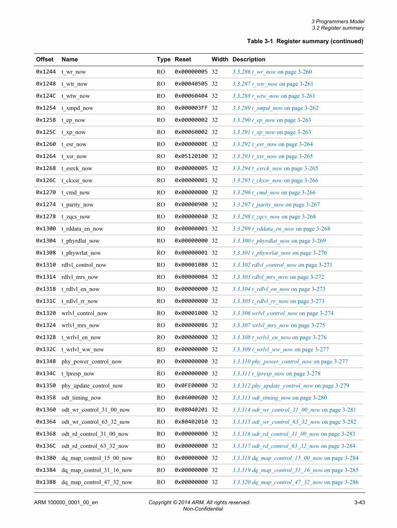
Table 3-1 Register summary (continued)
Offset Name Type Reset Width Description
0x1244 t_wr_now RO 0x00000005 32 3.3.286 t_wr_now on page 3-260
0x1248 t_wtr_now RO 0x00040505 32 3.3.287 t_wtr_now on page 3-261
0x124C t_wtw_now RO 0x00060404 32 3.3.288 t_wtw_now on page 3-261
0x1254 t_xmpd_now RO 0x000003FF 32 3.3.289 t_xmpd_now on page 3-262
0x1258 t_ep_now RO 0x00000002 32 3.3.290 t_ep_now on page 3-263
0x125C t_xp_now RO 0x00060002 32 3.3.291 t_xp_now on page 3-263
0x1260 t_esr_now RO 0x0000000E 32 3.3.292 t_esr_now on page 3-264
0x1264 t_xsr_now RO 0x05120100 32 3.3.293 t_xsr_now on page 3-265
0x1268 t_esrck_now RO 0x00000005 32 3.3.294 t_esrck_now on page 3-265
0x126C t_ckxsr_now RO 0x00000001 32 3.3.295 t_ckxsr_now on page 3-266
0x1270 t_cmd_now RO 0x00000000 32 3.3.296 t_cmd_now on page 3-266
0x1274 t_parity_now RO 0x00000900 32 3.3.297 t_parity_now on page 3-267
0x1278 t_zqcs_now RO 0x00000040 32 3.3.298 t_zqcs_now on page 3-268
0x1300 t_rddata_en_now RO 0x00000001 32 3.3.299 t_rddata_en_now on page 3-268
0x1304 t_phyrdlat_now RO 0x00000000 32 3.3.300 t_phyrdlat_now on page 3-269
0x1308 t_phywrlat_now RO 0x00000001 32 3.3.301 t_phywrlat_now on page 3-270
0x1310 rdlvl_control_now RO 0x00001080 32 3.3.302 rdlvl_control_now on page 3-271
0x1314 rdlvl_mrs_now RO 0x00000004 32 3.3.303 rdlvl_mrs_now on page 3-272
0x1318 t_rdlvl_en_now RO 0x00000000 32 3.3.304 t_rdlvl_en_now on page 3-273
0x131C t_rdlvl_rr_now RO 0x00000000 32 3.3.305 t_rdlvl_rr_now on page 3-273
0x1320 wrlvl_control_now RO 0x00001000 32 3.3.306 wrlvl_control_now on page 3-274
0x1324 wrlvl_mrs_now RO 0x00000086 32 3.3.307 wrlvl_mrs_now on page 3-275
0x1328 t_wrlvl_en_now RO 0x00000000 32 3.3.308 t_wrlvl_en_now on page 3-276
0x132C t_wrlvl_ww_now RO 0x00000000 32 3.3.309 t_wrlvl_ww_now on page 3-277
0x1348 phy_power_control_now RO 0x00000000 32 3.3.310 phy_power_control_now on page 3-277
0x134C t_lpresp_now RO 0x00000000 32 3.3.311 t_lpresp_now on page 3-278
0x1350 phy_update_control_now RO 0x0FE00000 32 3.3.312 phy_update_control_now on page 3-279
0x1358 odt_timing_now RO 0x06000600 32 3.3.313 odt_timing_now on page 3-280
0x1360 odt_wr_control_31_00_now RO 0x08040201 32 3.3.314 odt_wr_control_31_00_now on page 3-281
0x1364 odt_wr_control_63_32_now RO 0x80402010 32 3.3.315 odt_wr_control_63_32_now on page 3-282
0x1368 odt_rd_control_31_00_now RO 0x00000000 32 3.3.316 odt_rd_control_31_00_now on page 3-283
0x136C odt_rd_control_63_32_now RO 0x00000000 32 3.3.317 odt_rd_control_63_32_now on page 3-284
0x1380 dq_map_control_15_00_now RO 0x00000000 32 3.3.318 dq_map_control_15_00_now on page 3-284
0x1384 dq_map_control_31_16_now RO 0x00000000 32 3.3.319 dq_map_control_31_16_now on page 3-285
0x1388 dq_map_control_47_32_now RO 0x00000000 32 3.3.320 dq_map_control_47_32_now on page 3-286
3 Programmers Model3.2 Register summary
ARM 100000_0001_00_en Copyright © 2014 ARM. All rights reserved. 3-43Non-Confidential

Table 3-1 Register summary (continued)
Offset Name Type Reset Width Description
0x138C dq_map_control_63_48_now RO 0x00000000 32 3.3.321 dq_map_control_63_48_now on page 3-287
0x1390 dq_map_control_71_64_now RO 0x00000000 32 3.3.322 dq_map_control_71_64_now on page 3-288
0x1408 user_config0_now RO 0x00000000 32 3.3.323 user_config0_now on page 3-289
0x140C user_config1_now RO 0x00000000 32 3.3.324 user_config1_now on page 3-290
0x1FD0 periph_id_4 RO 0x00000014 32 3.3.325 periph_id_4 on page 3-290
0x1FE0 periph_id_0 RO 0x00000052 32 3.3.326 periph_id_0 on page 3-291
0x1FE4 periph_id_1 RO 0x000000B4 32 3.3.327 periph_id_1 on page 3-291
0x1FE8 periph_id_2 RO 0x0000001B 32 3.3.328 periph_id_2 on page 3-292
0x1FEC periph_id_3 RO 0x00000000 32 3.3.329 periph_id_3 on page 3-292
0x1FF0 component_id_0 RO 0x0000000D 32 3.3.330 component_id_0 on page 3-293
0x1FF4 component_id_1 RO 0x000000F0 32 3.3.331 component_id_1 on page 3-293
0x1FF8 component_id_2 RO 0x00000005 32 3.3.332 component_id_2 on page 3-294
0x1FFC component_id_3 RO 0x000000B1 32 3.3.333 component_id_3 on page 3-295
3 Programmers Model3.2 Register summary
ARM 100000_0001_00_en Copyright © 2014 ARM. All rights reserved. 3-44Non-Confidential

3.3 Register descriptionsThis section describes the DMC-520 registers.
3.2 Register summary on page 3-33 provides cross references to individual registers.
3.3.1 memc_status
Holds the architectural status of the DMC.
The memc_status register characteristics are:
Usage constraintsCan be read from when in ALL states. Cannot be changed.
ConfigurationsThere is only one DMC configuration.
Attributes
Offset 0x000
Type Read-onlyReset 0x00000000
Width 32
The following figure shows the bit assignments.
31 30 29 28 27 26 25 24 23 22 21 20 19 18 17 16 15 13 12 11 10 9 8 7 6 4 3 2 0
dest_memc_statusReserved_1memc_status
Reserved_2mgr_active
geardown_statusReserved_3mgr_dci_failed
scrub_outstanding_trans0scrub_active0Reserved_4
scrub_active1scrub_outstanding_trans1
scrub_active3scrub_outstanding_trans2scrub_active2
scrub_outstanding_trans4scrub_active4scrub_outstanding_trans3
scrub_active5scrub_outstanding_trans5
scrub_active7scrub_outstanding_trans6scrub_active6
scrub_outstanding_trans7
Figure 3-1 memc_status register bit assignments
The following shows the bit assignments.
[31] scrub_outstanding_trans7scrub_outstanding_trans7 bitfield.
3 Programmers Model3.3 Register descriptions
ARM 100000_0001_00_en Copyright © 2014 ARM. All rights reserved. 3-45Non-Confidential

[30] scrub_active7scrub_active7 bitfield.
[29] scrub_outstanding_trans6scrub_outstanding_trans6 bitfield.
[28] scrub_active6scrub_active6 bitfield.
[27] scrub_outstanding_trans5scrub_outstanding_trans5 bitfield.
[26] scrub_active5scrub_active5 bitfield.
[25] scrub_outstanding_trans4scrub_outstanding_trans4 bitfield.
[24] scrub_active4scrub_active4 bitfield.
[23] scrub_outstanding_trans3scrub_outstanding_trans3 bitfield.
[22] scrub_active3scrub_active3 bitfield.
[21] scrub_outstanding_trans2scrub_outstanding_trans2 bitfield.
[20] scrub_active2scrub_active2 bitfield.
[19] scrub_outstanding_trans1scrub_outstanding_trans1 bitfield.
[18] scrub_active1scrub_active1 bitfield.
[17] scrub_outstanding_trans0scrub_outstanding_trans0 bitfield.
[16] scrub_active0scrub_active0 bitfield.
[15:13] Reserved_4Unused bits
[12] geardown_statusIndicates if the DMC is operating in Geardown mode for DDR4 accesses.
[11:10] Reserved_3Unused bits
[9] mgr_dci_failedA direct command in a previous sequence has failed.
[8] mgr_activemgr_active bitfield.
[7] Reserved_2Unused bits
[6:4] dest_memc_statusThe intended destination state of the DMC during an active transition, or when in theABORTED or RECOVER state.
[3] Reserved_1Unused bits
[2:0] memc_statusThe current state of the DMC.
3.3.2 memc_config
Holds the configuration data for the DMC.
The memc_config register characteristics are:
Usage constraintsCan be read from when in ALL states. Cannot be changed.
3 Programmers Model3.3 Register descriptions
ARM 100000_0001_00_en Copyright © 2014 ARM. All rights reserved. 3-46Non-Confidential

ConfigurationsThere is only one DMC configuration.
Attributes
Offset 0x004
Type Read-onlyReset 0x00000000
Width 32
The following figure shows the bit assignments.
31 29 28 27 26 25 24 23 19 18 16 15 14 13 12 11 10 9 8 7 0
Reserved_1Reserved_4
memory_chip_selects_cfgReserved_2phy_data_width_cfg
Reserved_3queue_depth_cfg
memory_ecc_cfgReserved_5dmc_burst_length_cfg
Reserved_6
Figure 3-2 memc_config register bit assignments
The following shows the bit assignments.
[31:29] Reserved_6Unused bits
[28] memory_ecc_cfgIndicates presence of error correction code logic
[27:26] Reserved_5Unused bits
[25:24] dmc_burst_length_cfgConfigured DMC burst length, expressed in beats of phy_data_width_cfg width
[23:19] Reserved_4Unused bits
[18:16] queue_depth_cfgConfigured depth of the request queue, in units of DMC bursts
[15:14] Reserved_3Unused bits
[13:12] memory_chip_selects_cfgConfigured number of memory chip (rank) selects per interface
[11:10] Reserved_2Unused bits
[9:8] phy_data_width_cfgConfigured effective memory width, PHY interface width
[7:0] Reserved_1Unused bits
3.3.3 memc_cmd
Used to change the architectural state of the DMC, or execute queued manager operations.
The memc_cmd register characteristics are:
Usage constraintsCannot be read from. Can be written to when in ALL states.
3 Programmers Model3.3 Register descriptions
ARM 100000_0001_00_en Copyright © 2014 ARM. All rights reserved. 3-47Non-Confidential

ConfigurationsThere is only one DMC configuration.
Attributes
Offset 0x008
Type Write-onlyReset 0x00000000
Width 32
The following figure shows the bit assignments.
31 3 2 0
Reserved_1
memc_cmd
Figure 3-3 memc_cmd register bit assignments
The following shows the bit assignments.
[31:3] Reserved_1Unused bits
[2:0] memc_cmdmemc_cmd bitfield.
3.3.4 address_control_next
Configures the DRAM address parameters. Use the DRAM device data sheet or Serial Presence Detect(SPD)-derived values to assist in programming these values.
The address_control_next register characteristics are:
Usage constraintsCan be read from when in ALL states. Can be written to when in ALL states.
ConfigurationsThere is only one DMC configuration.
Attributes
Offset 0x010
Type Read-writeReset 0x00030202
Width 32
The following figure shows the bit assignments.
31 29 28 27 26 25 24 23 19 18 16 15 11 10 8 7 3 2 0
Reserved_1Reserved_2Reserved_3
bank_bits_nextrow_bits_nextcolumn_bits_next
rank_bits_nextReserved_4
Reserved_5bank_hash_enable_next
Figure 3-4 address_control_next register bit assignments
The following shows the bit assignments.
3 Programmers Model3.3 Register descriptions
ARM 100000_0001_00_en Copyright © 2014 ARM. All rights reserved. 3-48Non-Confidential

[31:29] Reserved_5Unused bits
[28] bank_hash_enable_nextConfigures the bank hash function used in system address decode. Used to alter trafficdistribution across banks.
[27:26] Reserved_4Unused bits
[25:24] rank_bits_nextProgram to match the number of active ranks to be addressed.
[23:19] Reserved_3Unused bits
[18:16] bank_bits_nextProgram to match the number of banks per chip-select (rank) on the attached DRAM device.
Note
This number corresponds to the sum total of all banks in all bank groups (where applicable) on adevice.
[15:11] Reserved_2Unused bits
[10:8] row_bits_nextProgram to match the number of row bits on the attached DRAM device.
[7:3] Reserved_1Unused bits
[2:0] column_bits_nextProgram to match the number of column address bits present on the DRAM device.
3.3.5 decode_control_next
Configures how the DRAM address is decoded from the system address. The DRAM address consists ofthe rank, bank, row address, and the column address.
The decode_control_next register characteristics are:
Usage constraintsCan be read from when in ALL states. Can be written to when in ALL states.
ConfigurationsThere is only one DMC configuration.
Attributes
Offset 0x014
Type Read-writeReset 0x00000000
Width 32
The following figure shows the bit assignments.
31 7 6 4 3 2 1 0
Reserved_2
stripe_decode_nextReserved_1address_decode_next
Figure 3-5 decode_control_next register bit assignments
The following shows the bit assignments.
3 Programmers Model3.3 Register descriptions
ARM 100000_0001_00_en Copyright © 2014 ARM. All rights reserved. 3-49Non-Confidential

[31:7] Reserved_2Unused bits
[6:4] stripe_decode_nextDetermines the address boundary on which to stripe system requests across DRAM pages. TheDMC decodes the bottom two page address bits from a programmable slice within the lowest 14bits of the system address. To disable sub-page striping you must program this value to theDRAM page size (or use the default value 0).
Note
You must not program the DMC to stripe at a higher boundary than the DRAM page size.
[3:2] Reserved_1Unused bits
[1:0] address_decode_nextDetermines in which pattern the DRAM address components are decoded from the systemaddress.
3.3.6 address_map_next
Configures the system address mapping options.
The address_map_next register characteristics are:
Usage constraintsCan be read from when in ALL states. Can be written to when in ALL states.
ConfigurationsThere is only one DMC configuration.
Attributes
Offset 0x01C
Type Read-writeReset 0x00000000
Width 32
The following figure shows the bit assignments.
31 16 15 3 2 0
Reserved_1addr_map_mask_next
addr_map_mode_next
Figure 3-6 address_map_next register bit assignments
The following shows the bit assignments.
[31:16] addr_map_mask_nextConfigures the mask applied to system address bits [43:28]. The system address map uses upperaddress bits to select from multiple DMC instances in a system. The DMC must discard theseaddress bits that fall outside physical memory to decode correctly.
[15:3] Reserved_1Unused bits
[2:0] addr_map_mode_nextSelects the address translation mode. See the System Address Conversion section of the DesignManual for more information on address translation options.
3.3.7 low_power_control_next
Configures the low-power features of the DMC.
The low_power_control_next register characteristics are:
3 Programmers Model3.3 Register descriptions
ARM 100000_0001_00_en Copyright © 2014 ARM. All rights reserved. 3-50Non-Confidential

Usage constraintsCan be read from when in ALL states. Can be written to when in ALL states.
ConfigurationsThere is only one DMC configuration.
Attributes
Offset 0x020
Type Read-writeReset 0x00000020
Width 32
The following figure shows the bit assignments.
31 8 7 4 3 2 1 0
Reserved_2
auto_power_down_nextstop_mem_clock_sref_nextReserved_1
auto_self_refresh_nextasr_period_next
Figure 3-7 low_power_control_next register bit assignments
The following shows the bit assignments.
[31:8] Reserved_2Unused bits
[7:4] asr_period_nextProgram the number of tREFI intervals to wait without activity before placing the DRAM into aself-refresh state when auto_self_refresh is enabled. The supported range for this bitfield is1-15.
[3] auto_self_refresh_nextProgram to enable or disable placing a DRAM rank into a self-refresh state when the rank hasbeen idle for the amount of time that asr_period defines.
[2] auto_power_down_nextProgram to enable or disable placing the DRAM into a power-down state when idle.
[1] stop_mem_clock_sref_nextProgram to enable or disable stopping the DRAM clock when the memory device is in self-refresh, reset, or maximum power down.
[0] Reserved_1Unused bits
3.3.8 turnaround_control_next
Configures the settings for arbitration between read and write and rank to rank traffic on the DRAM bus.
The turnaround_control_next register characteristics are:
Usage constraintsCan be read from when in ALL states. Can be written to when in ALL states.
ConfigurationsThere is only one DMC configuration.
Attributes
Offset 0x028
Type Read-writeReset 0x0F0F0F0F
Width 32
3 Programmers Model3.3 Register descriptions
ARM 100000_0001_00_en Copyright © 2014 ARM. All rights reserved. 3-51Non-Confidential

The following figure shows the bit assignments.
31 30 29 28 27 24 23 20 19 16 15 12 11 8 7 4 3 0
turnaround_limit_m_nextReserved_1turnaround_limit_l_next
Reserved_2turnaround_limit_h_next
Reserved_4turnaround_limit_hh_nextReserved_3
turnaround_prescalar_next
Figure 3-8 turnaround_control_next register bit assignments
The following shows the bit assignments.
[31:30] turnaround_prescalar_nextTurnaround counter prescaler.
[29:28] Reserved_4Unused bits
[27:24] turnaround_limit_hh_nextProgram the number of turnaround prescaler periods to wait between arbitrating a turnaround inthe presence of HIGH-HIGH class requests. The supported range for this bitfield is 0-15.
[23:20] Reserved_3Unused bits
[19:16] turnaround_limit_h_nextProgram the number of turnaround prescaler periods to wait between arbitrating a turnaround inthe presence of HIGH class requests. The supported range for this bitfield is 0-15.
[15:12] Reserved_2Unused bits
[11:8] turnaround_limit_m_nextProgram the number of turnaround prescaler periods to wait between arbitrating a turnaround inthe presence of MEDIUM class requests. The supported range for this bitfield is 0-15.
[7:4] Reserved_1Unused bits
[3:0] turnaround_limit_l_nextProgram the number of turnaround prescaler periods to wait between arbitrating a turnaround inthe presence of LOW class requests. The supported range for this bitfield is 0-15.
3.3.9 hit_turnaround_control_next
Configures the settings for preventing starvation of non-hits in the presence of in-row hit streams.
The hit_turnaround_control_next register characteristics are:
Usage constraintsCan be read from when in ALL states. Can be written to when in ALL states.
ConfigurationsThere is only one DMC configuration.
Attributes
Offset 0x02C
Type Read-writeReset 0x08909FBF
Width 32
3 Programmers Model3.3 Register descriptions
ARM 100000_0001_00_en Copyright © 2014 ARM. All rights reserved. 3-52Non-Confidential

The following figure shows the bit assignments.
31 30 29 24 23 22 21 16 15 14 13 8 7 6 5 0
hits_mask_l_nextReserved_1hit_turnaround_limit_l_next
hit_turnaround_limit_m_nextReserved_2
Reserved_3hit_turnaround_limit_h_nexthits_mask_m_next
Reserved_4hit_turnaround_limit_hh_nexthits_mask_h_next
hits_mask_hh_next
Figure 3-9 hit_turnaround_control_next register bit assignments
The following shows the bit assignments.
[31] hits_mask_hh_nextProgram to determine if DRAM row hits are prioritised over HIGH-HIGH priority traffic.
[30] Reserved_4Unused bits
[29:24] hit_turnaround_limit_hh_nextProgram the maximum number of consecutive in-row hits in the presence of HIGH-HIGH classrequests. Zero disables the hit limit function. The supported range for this bitfield is 0-63.
[23] hits_mask_h_nextProgram to determine if DRAM row hits are prioritised over HIGH priority traffic.
[22] Reserved_3Unused bits
[21:16] hit_turnaround_limit_h_nextProgram the maximum number of consecutive in-row hits in the presence of HIGH classrequests. Zero disables the hit limit function. The supported range for this bitfield is 0-63.
[15] hits_mask_m_nextProgram to determine if DRAM row hits are prioritised over MEDIUM priority traffic.
[14] Reserved_2Unused bits
[13:8] hit_turnaround_limit_m_nextProgram the maximum number of consecutive in-row hits in the presence of MEDIUM classrequests. Zero disables the hit limit function. The supported range for this bitfield is 0-63.
[7] hits_mask_l_nextProgram to determine if DRAM row hits are prioritised over LOW priority traffic.
[6] Reserved_1Unused bits
[5:0] hit_turnaround_limit_l_nextProgram the maximum number of consecutive in-row hits in the presence of LOW classrequests. Zero disables the hit limit function. The supported range for this bitfield is 0-63.
3.3.10 qos_class_control_next
Configures the priority class for each QoS encoding.
The qos_class_control_next register characteristics are:
Usage constraintsCan be read from when in ALL states. Can be written to when in ALL states.
3 Programmers Model3.3 Register descriptions
ARM 100000_0001_00_en Copyright © 2014 ARM. All rights reserved. 3-53Non-Confidential

ConfigurationsThere is only one DMC configuration.
Attributes
Offset 0x030
Type Read-writeReset 0x00000FC8
Width 32
The following figure shows the bit assignments.
31 12 11 8 7 4 3 0
Reserved_1
high_high_qos_start_nexthigh_qos_start_nextmedium_qos_start_next
Figure 3-10 qos_class_control_next register bit assignments
The following shows the bit assignments.
[31:12] Reserved_1Unused bits
[11:8] high_high_qos_start_nextDetermines the minimum Qv value mapped onto the HIGH-HIGH QoS class. The supportedrange for this bitfield is 0-15.
[7:4] high_qos_start_nextDetermines the minimum Qv value mapped onto the HIGH QoS class. The supported range forthis bitfield is 0-15.
[3:0] medium_qos_start_nextDetermines the minimum Qv value mapped onto the MEDIUM QoS class. The supported rangefor this bitfield is 0-15.
3.3.11 escalation_control_next
Configures the settings for escalating the priority of entries in the queue.
The escalation_control_next register characteristics are:
Usage constraintsCan be read from when in ALL states. Can be written to when in ALL states.
ConfigurationsThere is only one DMC configuration.
Attributes
Offset 0x034
Type Read-writeReset 0x00080000
Width 32
The following figure shows the bit assignments.
3 Programmers Model3.3 Register descriptions
ARM 100000_0001_00_en Copyright © 2014 ARM. All rights reserved. 3-54Non-Confidential

31 20 19 16 15 12 11 8 7 2 1 0
Reserved_1Reserved_3
Reserved_2escalation_count_nextescalation_prescalar_next
read_backlog_suppression_next
Figure 3-11 escalation_control_next register bit assignments
The following shows the bit assignments.
[31:20] Reserved_3Unused bits
[19:16] read_backlog_suppression_nextConfigures the number of completed reads (as a proportion in 16ths of the queue depth) atwhich to stop arbitrating more reads until the system drains the fetched read data. Zero disablesthis feature. The supported range for this bitfield is 0-15.
[15:12] Reserved_2Unused bits
[11:8] escalation_count_nextProgram the number of escalation prescaler periods between applying escalation. Zero disablespriority escalation in the queue. The supported range for this bitfield is 0-15.
[7:2] Reserved_1Unused bits
[1:0] escalation_prescalar_nextEscalation counter prescaler.
3.3.12 qv_control_31_00_next
Configures the priority settings for each QoS encoding.
The qv_control_31_00_next register characteristics are:
Usage constraintsCan be read from when in ALL states. Can be written to when in ALL states.
ConfigurationsThere is only one DMC configuration.
Attributes
Offset 0x038
Type Read-writeReset 0x76543210
Width 32
The following figure shows the bit assignments.
3 Programmers Model3.3 Register descriptions
ARM 100000_0001_00_en Copyright © 2014 ARM. All rights reserved. 3-55Non-Confidential

31 28 27 24 23 20 19 16 15 12 11 8 7 4 3 0
qos2_priority_nextqos1_priority_nextqos0_priority_next
qos3_priority_nextqos4_priority_next
qos7_priority_nextqos6_priority_nextqos5_priority_next
Figure 3-12 qv_control_31_00_next register bit assignments
The following shows the bit assignments.
[31:28] qos7_priority_nextProgram the queueing priority for requests received with this QoS value. The supported rangefor this bitfield is 0-15.
[27:24] qos6_priority_nextProgram the queueing priority for requests received with this QoS value. The supported rangefor this bitfield is 0-15.
[23:20] qos5_priority_nextProgram the queueing priority for requests received with this QoS value. The supported rangefor this bitfield is 0-15.
[19:16] qos4_priority_nextProgram the queueing priority for requests received with this QoS value. The supported rangefor this bitfield is 0-15.
[15:12] qos3_priority_nextProgram the queueing priority for requests received with this QoS value. The supported rangefor this bitfield is 0-15.
[11:8] qos2_priority_nextProgram the queueing priority for requests received with this QoS value. The supported rangefor this bitfield is 0-15.
[7:4] qos1_priority_nextProgram the queueing priority for requests received with this QoS value. The supported rangefor this bitfield is 0-15.
[3:0] qos0_priority_nextProgram the queueing priority for requests received with this QoS value. The supported rangefor this bitfield is 0-15.
3.3.13 qv_control_63_32_next
Configures the priority settings for each QoS encoding.
The qv_control_63_32_next register characteristics are:
Usage constraintsCan be read from when in ALL states. Can be written to when in ALL states.
ConfigurationsThere is only one DMC configuration.
Attributes
Offset 0x03C
Type Read-writeReset 0xFEDCBA98
Width 32
The following figure shows the bit assignments.
3 Programmers Model3.3 Register descriptions
ARM 100000_0001_00_en Copyright © 2014 ARM. All rights reserved. 3-56Non-Confidential

31 28 27 24 23 20 19 16 15 12 11 8 7 4 3 0
qos10_priority_nextqos9_priority_nextqos8_priority_next
qos11_priority_nextqos12_priority_next
qos15_priority_nextqos14_priority_nextqos13_priority_next
Figure 3-13 qv_control_63_32_next register bit assignments
The following shows the bit assignments.
[31:28] qos15_priority_nextProgram the queueing priority for requests received with this QoS value. The supported rangefor this bitfield is 0-15.
[27:24] qos14_priority_nextProgram the queueing priority for requests received with this QoS value. The supported rangefor this bitfield is 0-15.
[23:20] qos13_priority_nextProgram the queueing priority for requests received with this QoS value. The supported rangefor this bitfield is 0-15.
[19:16] qos12_priority_nextProgram the queueing priority for requests received with this QoS value. The supported rangefor this bitfield is 0-15.
[15:12] qos11_priority_nextProgram the queueing priority for requests received with this QoS value. The supported rangefor this bitfield is 0-15.
[11:8] qos10_priority_nextProgram the queueing priority for requests received with this QoS value. The supported rangefor this bitfield is 0-15.
[7:4] qos9_priority_nextProgram the queueing priority for requests received with this QoS value. The supported rangefor this bitfield is 0-15.
[3:0] qos8_priority_nextProgram the queueing priority for requests received with this QoS value. The supported rangefor this bitfield is 0-15.
3.3.14 rt_control_31_00_next
Configures the timeout settings for each QoS encoding.
The rt_control_31_00_next register characteristics are:
Usage constraintsCan be read from when in ALL states. Can be written to when in ALL states.
ConfigurationsThere is only one DMC configuration.
Attributes
Offset 0x040
Type Read-writeReset 0x00000000
Width 32
The following figure shows the bit assignments.
3 Programmers Model3.3 Register descriptions
ARM 100000_0001_00_en Copyright © 2014 ARM. All rights reserved. 3-57Non-Confidential

31 28 27 24 23 20 19 16 15 12 11 8 7 4 3 0
qos2_timeout_nextqos1_timeout_nextqos0_timeout_next
qos3_timeout_nextqos4_timeout_next
qos7_timeout_nextqos6_timeout_nextqos5_timeout_next
Figure 3-14 rt_control_31_00_next register bit assignments
The following shows the bit assignments.
[31:28] qos7_timeout_nextProgram the number of timeout prescaler periods to wait before elevating a received request tomaximum priority. Zero disables this feature for request received with this QoS value. Thesupported range for this bitfield is 0-15.
[27:24] qos6_timeout_nextProgram the number of timeout prescaler periods to wait before elevating a received request tomaximum priority. Zero disables this feature for request received with this QoS value. Thesupported range for this bitfield is 0-15.
[23:20] qos5_timeout_nextProgram the number of timeout prescaler periods to wait before elevating a received request tomaximum priority. Zero disables this feature for request received with this QoS value. Thesupported range for this bitfield is 0-15.
[19:16] qos4_timeout_nextProgram the number of timeout prescaler periods to wait before elevating a received request tomaximum priority. Zero disables this feature for request received with this QoS value. Thesupported range for this bitfield is 0-15.
[15:12] qos3_timeout_nextProgram the number of timeout prescaler periods to wait before elevating a received request tomaximum priority. Zero disables this feature for request received with this QoS value. Thesupported range for this bitfield is 0-15.
[11:8] qos2_timeout_nextProgram the number of timeout prescaler periods to wait before elevating a received request tomaximum priority. Zero disables this feature for request received with this QoS value. Thesupported range for this bitfield is 0-15.
[7:4] qos1_timeout_nextProgram the number of timeout prescaler periods to wait before elevating a received request tomaximum priority. Zero disables this feature for request received with this QoS value. Thesupported range for this bitfield is 0-15.
[3:0] qos0_timeout_nextProgram the number of timeout prescaler periods to wait before elevating a received request tomaximum priority. Zero disables this feature for request received with this QoS value. Thesupported range for this bitfield is 0-15.
3.3.15 rt_control_63_32_next
Configures the timeout settings for each QoS encoding.
The rt_control_63_32_next register characteristics are:
Usage constraintsCan be read from when in ALL states. Can be written to when in ALL states.
ConfigurationsThere is only one DMC configuration.
3 Programmers Model3.3 Register descriptions
ARM 100000_0001_00_en Copyright © 2014 ARM. All rights reserved. 3-58Non-Confidential

Attributes
Offset 0x044
Type Read-writeReset 0x00000000
Width 32
The following figure shows the bit assignments.
31 28 27 24 23 20 19 16 15 12 11 8 7 4 3 0
qos10_timeout_nextqos9_timeout_nextqos8_timeout_next
qos11_timeout_nextqos12_timeout_next
qos15_timeout_nextqos14_timeout_nextqos13_timeout_next
Figure 3-15 rt_control_63_32_next register bit assignments
The following shows the bit assignments.
[31:28] qos15_timeout_nextProgram the number of timeout prescaler periods to wait before elevating a received request tomaximum priority. Zero disables this feature for request received with this QoS value. Thesupported range for this bitfield is 0-15.
[27:24] qos14_timeout_nextProgram the number of timeout prescaler periods to wait before elevating a received request tomaximum priority. Zero disables this feature for request received with this QoS value. Thesupported range for this bitfield is 0-15.
[23:20] qos13_timeout_nextProgram the number of timeout prescaler periods to wait before elevating a received request tomaximum priority. Zero disables this feature for request received with this QoS value. Thesupported range for this bitfield is 0-15.
[19:16] qos12_timeout_nextProgram the number of timeout prescaler periods to wait before elevating a received request tomaximum priority. Zero disables this feature for request received with this QoS value. Thesupported range for this bitfield is 0-15.
[15:12] qos11_timeout_nextProgram the number of timeout prescaler periods to wait before elevating a received request tomaximum priority. Zero disables this feature for request received with this QoS value. Thesupported range for this bitfield is 0-15.
[11:8] qos10_timeout_nextProgram the number of timeout prescaler periods to wait before elevating a received request tomaximum priority. Zero disables this feature for request received with this QoS value. Thesupported range for this bitfield is 0-15.
[7:4] qos9_timeout_nextProgram the number of timeout prescaler periods to wait before elevating a received request tomaximum priority. Zero disables this feature for request received with this QoS value. Thesupported range for this bitfield is 0-15.
[3:0] qos8_timeout_nextProgram the number of timeout prescaler periods to wait before elevating a received request tomaximum priority. Zero disables this feature for request received with this QoS value. Thesupported range for this bitfield is 0-15.
3 Programmers Model3.3 Register descriptions
ARM 100000_0001_00_en Copyright © 2014 ARM. All rights reserved. 3-59Non-Confidential

3.3.16 timeout_control_next
Configures the prescaler applied to timeout values.
The timeout_control_next register characteristics are:
Usage constraintsCan be read from when in ALL states. Can be written to when in ALL states.
ConfigurationsThere is only one DMC configuration.
Attributes
Offset 0x048
Type Read-writeReset 0x00000001
Width 32
The following figure shows the bit assignments.
31 2 1 0
Reserved_1
timeout_prescalar_next
Figure 3-16 timeout_control_next register bit assignments
The following shows the bit assignments.
[31:2] Reserved_1Unused bits
[1:0] timeout_prescalar_nexttimeout_prescalar_next bitfield.
3.3.17 credit_control_next
Configures the settings for preventing starvation of CHI protocol retries.
The credit_control_next register characteristics are:
Usage constraintsCan be read from when in ALL states. Can be written to when in ALL states.
ConfigurationsThere is only one DMC configuration.
Attributes
Offset 0x04C
Type Read-writeReset 0x00000000
Width 32
The following figure shows the bit assignments.
31 12 11 8 7 2 1 0
Reserved_1Reserved_2
credit_count_nextcredit_prescalar_next
Figure 3-17 credit_control_next register bit assignments
The following shows the bit assignments.
3 Programmers Model3.3 Register descriptions
ARM 100000_0001_00_en Copyright © 2014 ARM. All rights reserved. 3-60Non-Confidential

[31:12] Reserved_2Unused bits
[11:8] credit_count_nextProgram the number of P-credit prescaler periods between applying escalation. 0 disables thisfeature. The supported range for this bitfield is 0-15.
[7:2] Reserved_1Unused bits
[1:0] credit_prescalar_nextP-credit counter prescaler.
3.3.18 write_priority_control_31_00_next
Configures the priority settings for write requests within the DMC
The write_priority_control_31_00_next register characteristics are:
Usage constraintsCan be read from when in ALL states. Can be written to when in ALL states.
ConfigurationsThere is only one DMC configuration.
Attributes
Offset 0x050
Type Read-writeReset 0x00000000
Width 32
The following figure shows the bit assignments.
31 28 27 24 23 20 19 16 15 12 11 8 7 4 3 0
write_fill_priority_2_16ths_nextwrite_fill_priority_1_16ths_nextReserved_1
write_fill_priority_3_16ths_nextwrite_fill_priority_4_16ths_next
write_fill_priority_7_16ths_nextwrite_fill_priority_6_16ths_nextwrite_fill_priority_5_16ths_next
Figure 3-18 write_priority_control_31_00_next register bit assignments
The following shows the bit assignments.
[31:28] write_fill_priority_7_16ths_nextProgram the priority of write requests when write requests occupy 7/16ths of the DMC queue.The supported range for this bitfield is 0-15.
[27:24] write_fill_priority_6_16ths_nextProgram the priority of write requests when write requests occupy 6/16ths of the DMC queue.The supported range for this bitfield is 0-15.
[23:20] write_fill_priority_5_16ths_nextProgram the priority of write requests when write requests occupy 5/16ths of the DMC queue.The supported range for this bitfield is 0-15.
[19:16] write_fill_priority_4_16ths_nextProgram the priority of write requests when write requests occupy 4/16ths of the DMC queue.The supported range for this bitfield is 0-15.
3 Programmers Model3.3 Register descriptions
ARM 100000_0001_00_en Copyright © 2014 ARM. All rights reserved. 3-61Non-Confidential

[15:12] write_fill_priority_3_16ths_nextProgram the priority of write requests when write requests occupy 3/16ths of the DMC queue.The supported range for this bitfield is 0-15.
[11:8] write_fill_priority_2_16ths_nextProgram the priority of write requests when write requests occupy 2/16ths of the DMC queue.The supported range for this bitfield is 0-15.
[7:4] write_fill_priority_1_16ths_nextProgram the priority of write requests when write requests occupy 1/16th of the DMC queue.The supported range for this bitfield is 0-15.
[3:0] Reserved_1Unused bits
3.3.19 write_priority_control_63_32_next
Configures the priority settings for write requests within the DMC.
The write_priority_control_63_32_next register characteristics are:
Usage constraintsCan be read from when in ALL states. Can be written to when in ALL states.
ConfigurationsThere is only one DMC configuration.
Attributes
Offset 0x054
Type Read-writeReset 0x00000000
Width 32
The following figure shows the bit assignments.
31 28 27 24 23 20 19 16 15 12 11 8 7 4 3 0
write_fill_priority_10_16ths_nextwrite_fill_priority_9_16ths_nextwrite_fill_priority_8_16ths_next
write_fill_priority_11_16ths_nextwrite_fill_priority_12_16ths_next
write_fill_priority_15_16ths_nextwrite_fill_priority_14_16ths_nextwrite_fill_priority_13_16ths_next
Figure 3-19 write_priority_control_63_32_next register bit assignments
The following shows the bit assignments.
[31:28] write_fill_priority_15_16ths_nextProgram the priority of write requests when write requests occupy 15/16ths of the DMC queue.The supported range for this bitfield is 0-15.
[27:24] write_fill_priority_14_16ths_nextProgram the priority of write requests when write requests occupy 14/16ths of the DMC queue.The supported range for this bitfield is 0-15.
[23:20] write_fill_priority_13_16ths_nextProgram the priority of write requests when write requests occupy 13/16ths of the DMC queue.The supported range for this bitfield is 0-15.
[19:16] write_fill_priority_12_16ths_nextProgram the priority of write requests when write requests occupy 12/16ths of the DMC queue.The supported range for this bitfield is 0-15.
3 Programmers Model3.3 Register descriptions
ARM 100000_0001_00_en Copyright © 2014 ARM. All rights reserved. 3-62Non-Confidential

[15:12] write_fill_priority_11_16ths_nextProgram the priority of write requests when write requests occupy 11/16ths of the DMC queue.The supported range for this bitfield is 0-15.
[11:8] write_fill_priority_10_16ths_nextProgram the priority of write requests when write requests occupy 10/16ths of the DMC queue.The supported range for this bitfield is 0-15.
[7:4] write_fill_priority_9_16ths_nextProgram the priority of write requests when write requests occupy 9/16ths of the DMC queue.The supported range for this bitfield is 0-15.
[3:0] write_fill_priority_8_16ths_nextProgram the priority of write requests when write requests occupy 8/16ths of the DMC queue.The supported range for this bitfield is 0-15.
3.3.20 queue_threshold_control_31_00_next
Configures the threshold settings for requests in the DMC
The queue_threshold_control_31_00_next register characteristics are:
Usage constraintsCan be read from when in ALL states. Can be written to when in ALL states.
ConfigurationsThere is only one DMC configuration.
Attributes
Offset 0x060
Type Read-writeReset 0x00000000
Width 32
The following figure shows the bit assignments.
31 28 27 24 23 20 19 16 15 12 11 8 7 4 3 0
queue_fill_threshold_2_16ths_nextqueue_fill_threshold_1_16ths_nextReserved_1
queue_fill_threshold_3_16ths_nextqueue_fill_threshold_4_16ths_next
queue_fill_threshold_7_16ths_nextqueue_fill_threshold_6_16ths_nextqueue_fill_threshold_5_16ths_next
Figure 3-20 queue_threshold_control_31_00_next register bit assignments
The following shows the bit assignments.
[31:28] queue_fill_threshold_7_16ths_nextProgram to set the priority that requests must be equal to or above, to be accepted when thequeue is 7/16ths full. The supported range for this bitfield is 0-15.
[27:24] queue_fill_threshold_6_16ths_nextProgram to set the priority that requests must be equal to or above, to be accepted when thequeue is 6/16ths full. The supported range for this bitfield is 0-15.
[23:20] queue_fill_threshold_5_16ths_nextProgram to set the priority that requests must be equal to or above, to be accepted when thequeue is 5/16ths full. The supported range for this bitfield is 0-15.
3 Programmers Model3.3 Register descriptions
ARM 100000_0001_00_en Copyright © 2014 ARM. All rights reserved. 3-63Non-Confidential

[19:16] queue_fill_threshold_4_16ths_nextProgram to set the priority that requests must be equal to or above, to be accepted when thequeue is 4/16ths full. The supported range for this bitfield is 0-15.
[15:12] queue_fill_threshold_3_16ths_nextProgram to set the priority that requests must be equal to or above, to be accepted when thequeue is 3/16ths full. The supported range for this bitfield is 0-15.
[11:8] queue_fill_threshold_2_16ths_nextProgram to set the priority that requests must be equal to or above, to be accepted when thequeue is 2/16ths full. The supported range for this bitfield is 0-15.
[7:4] queue_fill_threshold_1_16ths_nextProgram to set the priority that requests must be equal to or above, to be accepted when thequeue is 1/16ths full. The supported range for this bitfield is 0-15.
[3:0] Reserved_1Unused bits
3.3.21 queue_threshold_control_63_32_next
Configures the threshold settings for requests in the DMC
The queue_threshold_control_63_32_next register characteristics are:
Usage constraintsCan be read from when in ALL states. Can be written to when in ALL states.
ConfigurationsThere is only one DMC configuration.
Attributes
Offset 0x064
Type Read-writeReset 0x00000000
Width 32
The following figure shows the bit assignments.
31 28 27 24 23 20 19 16 15 12 11 8 7 4 3 0
queue_fill_threshold_10_16ths_nextqueue_fill_threshold_9_16ths_nextqueue_fill_threshold_8_16ths_next
queue_fill_threshold_11_16ths_nextqueue_fill_threshold_12_16ths_next
queue_fill_threshold_15_16ths_nextqueue_fill_threshold_14_16ths_nextqueue_fill_threshold_13_16ths_next
Figure 3-21 queue_threshold_control_63_32_next register bit assignments
The following shows the bit assignments.
[31:28] queue_fill_threshold_15_16ths_nextProgram to set the priority that requests must be equal to or above, to be accepted when thequeue is 15/16ths full. The supported range for this bitfield is 0-15.
[27:24] queue_fill_threshold_14_16ths_nextProgram to set the priority that requests must be equal to or above, to be accepted when thequeue is 14/16ths full. The supported range for this bitfield is 0-15.
[23:20] queue_fill_threshold_13_16ths_nextProgram to set the priority that requests must be equal to or above, to be accepted when thequeue is 13/16ths full. The supported range for this bitfield is 0-15.
3 Programmers Model3.3 Register descriptions
ARM 100000_0001_00_en Copyright © 2014 ARM. All rights reserved. 3-64Non-Confidential

[19:16] queue_fill_threshold_12_16ths_nextProgram to set the priority that requests must be equal to or above, to be accepted when thequeue is 12/16ths full. The supported range for this bitfield is 0-15.
[15:12] queue_fill_threshold_11_16ths_nextProgram to set the priority that requests must be equal to or above, to be accepted when thequeue is 11/16ths full. The supported range for this bitfield is 0-15.
[11:8] queue_fill_threshold_10_16ths_nextProgram to set the priority that requests must be equal to or above, to be accepted when thequeue is 10/16ths full. The supported range for this bitfield is 0-15.
[7:4] queue_fill_threshold_9_16ths_nextProgram to set the priority that requests must be equal to or above, to be accepted when thequeue is 9/16ths full. The supported range for this bitfield is 0-15.
[3:0] queue_fill_threshold_8_16ths_nextProgram to set the priority that requests must be equal to or above, to be accepted when thequeue is 8/16ths full. The supported range for this bitfield is 0-15.
3.3.22 memory_address_max_31_00_next
Configures the address space control for the DMC default region.
The memory_address_max_31_00_next register characteristics are:
Usage constraintsCan be read from when in ALL states. Can be written to when in ALL states.
ConfigurationsThere is only one DMC configuration.
Attributes
Offset 0x078
Type Read-writeReset 0x00000010
Width 32
The following figure shows the bit assignments.
31 16 15 5 4 3 2 1 0
Reserved_1memory_address_max_31_16_next
region_s_read_en_nextregion_ns_write_en_nextregion_ns_read_en_next
region_s_write_en_nextenable_err_response_next
Figure 3-22 memory_address_max_31_00_next register bit assignments
The following shows the bit assignments.
[31:16] memory_address_max_31_16_nextProgram to set bits[31:16] of the maximum memory address.
Note
This is the address value after address translation has been applied (if applicable).
[15:5] Reserved_1Unused bits
[4] enable_err_response_nextConfigures the response used for a request that fails address access checks.
3 Programmers Model3.3 Register descriptions
ARM 100000_0001_00_en Copyright © 2014 ARM. All rights reserved. 3-65Non-Confidential

[3] region_s_write_en_nextEnables Secure writes to the default region
[2] region_s_read_en_nextEnables Secure reads to the default region
[1] region_ns_write_en_nextEnables Non-secure writes to the default region
[0] region_ns_read_en_nextEnables Non-secure reads to the default region
3.3.23 memory_address_max_43_32_next
Configures the address space control for the DMC default region.
The memory_address_max_43_32_next register characteristics are:
Usage constraintsCan be read from when in ALL states. Can be written to when in ALL states.
ConfigurationsThere is only one DMC configuration.
Attributes
Offset 0x07C
Type Read-writeReset 0x00000000
Width 32
The following figure shows the bit assignments.
31 12 11 0
Reserved_1
memory_address_max_43_32_next
Figure 3-23 memory_address_max_43_32_next register bit assignments
The following shows the bit assignments.
[31:12] Reserved_1Unused bits
[11:0] memory_address_max_43_32_nextProgram to set bits[43:32] of the maximum memory address.
Note
This is the address value after address translation has been applied (if applicable).
3.3.24 access_address_min0_31_00_next
Configures the address space control for address region 0.
The access_address_min0_31_00_next register characteristics are:
Usage constraintsCan be read from when in ALL states. Can be written to when in ALL states.
ConfigurationsThere is only one DMC configuration.
Attributes
Offset 0x080
Type Read-write
3 Programmers Model3.3 Register descriptions
ARM 100000_0001_00_en Copyright © 2014 ARM. All rights reserved. 3-66Non-Confidential

Reset 0x00000000
Width 32
The following figure shows the bit assignments.
31 16 15 4 3 2 1 0
Reserved_1access_address_min0_31_16_next
region_s_read_en0_nextregion_ns_write_en0_nextregion_ns_read_en0_next
region_s_write_en0_next
Figure 3-24 access_address_min0_31_00_next register bit assignments
The following shows the bit assignments.
[31:16] access_address_min0_31_16_nextProgram to set bits[31:16] of the minimum address in the region
[15:4] Reserved_1Unused bits
[3] region_s_write_en0_nextEnables Secure writes to the region
[2] region_s_read_en0_nextEnables Secure reads to the region
[1] region_ns_write_en0_nextEnables Non-secure writes to the region
[0] region_ns_read_en0_nextEnables Non-secure reads to the region
3.3.25 access_address_min0_43_32_next
Configures the address space control for address region 0.
The access_address_min0_43_32_next register characteristics are:
Usage constraintsCan be read from when in ALL states. Can be written to when in ALL states.
ConfigurationsThere is only one DMC configuration.
Attributes
Offset 0x084
Type Read-writeReset 0x00000000
Width 32
The following figure shows the bit assignments.
31 12 11 0
Reserved_1
access_address_min0_43_32_next
Figure 3-25 access_address_min0_43_32_next register bit assignments
The following shows the bit assignments.
[31:12] Reserved_1Unused bits
3 Programmers Model3.3 Register descriptions
ARM 100000_0001_00_en Copyright © 2014 ARM. All rights reserved. 3-67Non-Confidential

[11:0] access_address_min0_43_32_nextProgram to set bits[43:32] of the minimum address in the region
3.3.26 access_address_max0_31_00_next
Configures the address space control for address region 0.
The access_address_max0_31_00_next register characteristics are:
Usage constraintsCan be read from when in ALL states. Can be written to when in ALL states.
ConfigurationsThere is only one DMC configuration.
Attributes
Offset 0x088
Type Read-writeReset 0x00000000
Width 32
The following figure shows the bit assignments.
31 16 15 0
Reserved_1access_address_max0_31_16_next
Figure 3-26 access_address_max0_31_00_next register bit assignments
The following shows the bit assignments.
[31:16] access_address_max0_31_16_nextProgram to set bits[31:16] of the maximum address in the region
[15:0] Reserved_1Unused bits
3.3.27 access_address_max0_43_32_next
Configures the address space control for address region 0.
The access_address_max0_43_32_next register characteristics are:
Usage constraintsCan be read from when in ALL states. Can be written to when in ALL states.
ConfigurationsThere is only one DMC configuration.
Attributes
Offset 0x08C
Type Read-writeReset 0x00000000
Width 32
The following figure shows the bit assignments.
31 12 11 0
Reserved_1
access_address_max0_43_32_next
Figure 3-27 access_address_max0_43_32_next register bit assignments
The following shows the bit assignments.
3 Programmers Model3.3 Register descriptions
ARM 100000_0001_00_en Copyright © 2014 ARM. All rights reserved. 3-68Non-Confidential

[31:12] Reserved_1Unused bits
[11:0] access_address_max0_43_32_nextProgram to set bits[43:32] of the maximum address in the region
3.3.28 access_address_min1_31_00_next
Configures the address space control for address region 1.
The access_address_min1_31_00_next register characteristics are:
Usage constraintsCan be read from when in ALL states. Can be written to when in ALL states.
ConfigurationsThere is only one DMC configuration.
Attributes
Offset 0x090
Type Read-writeReset 0x00000000
Width 32
The following figure shows the bit assignments.
31 16 15 4 3 2 1 0
Reserved_1access_address_min1_31_16_next
region_s_read_en1_nextregion_ns_write_en1_nextregion_ns_read_en1_next
region_s_write_en1_next
Figure 3-28 access_address_min1_31_00_next register bit assignments
The following shows the bit assignments.
[31:16] access_address_min1_31_16_nextProgram to set bits[31:16] of the minimum address in the region
[15:4] Reserved_1Unused bits
[3] region_s_write_en1_nextEnables Secure writes to the region
[2] region_s_read_en1_nextEnables Secure reads to the region
[1] region_ns_write_en1_nextEnables Non-secure writes to the region
[0] region_ns_read_en1_nextEnables Non-secure reads to the region
3.3.29 access_address_min1_43_32_next
Configures the address space control for address region 1.
The access_address_min1_43_32_next register characteristics are:
Usage constraintsCan be read from when in ALL states. Can be written to when in ALL states.
ConfigurationsThere is only one DMC configuration.
Attributes
3 Programmers Model3.3 Register descriptions
ARM 100000_0001_00_en Copyright © 2014 ARM. All rights reserved. 3-69Non-Confidential

Offset 0x094
Type Read-writeReset 0x00000000
Width 32
The following figure shows the bit assignments.
31 12 11 0
Reserved_1
access_address_min1_43_32_next
Figure 3-29 access_address_min1_43_32_next register bit assignments
The following shows the bit assignments.
[31:12] Reserved_1Unused bits
[11:0] access_address_min1_43_32_nextProgram to set bits[43:32] of the minimum address in the region
3.3.30 access_address_max1_31_00_next
Configures the address space control for address region 1.
The access_address_max1_31_00_next register characteristics are:
Usage constraintsCan be read from when in ALL states. Can be written to when in ALL states.
ConfigurationsThere is only one DMC configuration.
Attributes
Offset 0x098
Type Read-writeReset 0x00000000
Width 32
The following figure shows the bit assignments.
31 16 15 0
Reserved_1access_address_max1_31_16_next
Figure 3-30 access_address_max1_31_00_next register bit assignments
The following shows the bit assignments.
[31:16] access_address_max1_31_16_nextProgram to set bits[31:16] of the maximum address in the region
[15:0] Reserved_1Unused bits
3.3.31 access_address_max1_43_32_next
Configures the address space control for address region 1.
The access_address_max1_43_32_next register characteristics are:
Usage constraintsCan be read from when in ALL states. Can be written to when in ALL states.
3 Programmers Model3.3 Register descriptions
ARM 100000_0001_00_en Copyright © 2014 ARM. All rights reserved. 3-70Non-Confidential

ConfigurationsThere is only one DMC configuration.
Attributes
Offset 0x09C
Type Read-writeReset 0x00000000
Width 32
The following figure shows the bit assignments.
31 12 11 0
Reserved_1
access_address_max1_43_32_next
Figure 3-31 access_address_max1_43_32_next register bit assignments
The following shows the bit assignments.
[31:12] Reserved_1Unused bits
[11:0] access_address_max1_43_32_nextProgram to set bits[43:32] of the maximum address in the region
3.3.32 access_address_min2_31_00_next
Configures the address space control for address region 2.
The access_address_min2_31_00_next register characteristics are:
Usage constraintsCan be read from when in ALL states. Can be written to when in ALL states.
ConfigurationsThere is only one DMC configuration.
Attributes
Offset 0x0A0
Type Read-writeReset 0x00000000
Width 32
The following figure shows the bit assignments.
31 16 15 4 3 2 1 0
Reserved_1access_address_min2_31_16_next
region_s_read_en2_nextregion_ns_write_en2_nextregion_ns_read_en2_next
region_s_write_en2_next
Figure 3-32 access_address_min2_31_00_next register bit assignments
The following shows the bit assignments.
[31:16] access_address_min2_31_16_nextProgram to set bits[31:16] of the minimum address in the region
[15:4] Reserved_1Unused bits
3 Programmers Model3.3 Register descriptions
ARM 100000_0001_00_en Copyright © 2014 ARM. All rights reserved. 3-71Non-Confidential

[3] region_s_write_en2_nextEnables Secure writes to the region
[2] region_s_read_en2_nextEnables Secure reads to the region
[1] region_ns_write_en2_nextEnables Non-secure writes to the region
[0] region_ns_read_en2_nextEnables Non-secure reads to the region
3.3.33 access_address_min2_43_32_next
Configures the address space control for address region 2.
The access_address_min2_43_32_next register characteristics are:
Usage constraintsCan be read from when in ALL states. Can be written to when in ALL states.
ConfigurationsThere is only one DMC configuration.
Attributes
Offset 0x0A4
Type Read-writeReset 0x00000000
Width 32
The following figure shows the bit assignments.
31 12 11 0
Reserved_1
access_address_min2_43_32_next
Figure 3-33 access_address_min2_43_32_next register bit assignments
The following shows the bit assignments.
[31:12] Reserved_1Unused bits
[11:0] access_address_min2_43_32_nextProgram to set bits[43:32] of the minimum address in the region
3.3.34 access_address_max2_31_00_next
Configures the address space control for address region 2.
The access_address_max2_31_00_next register characteristics are:
Usage constraintsCan be read from when in ALL states. Can be written to when in ALL states.
ConfigurationsThere is only one DMC configuration.
Attributes
Offset 0x0A8
Type Read-writeReset 0x00000000
Width 32
The following figure shows the bit assignments.
3 Programmers Model3.3 Register descriptions
ARM 100000_0001_00_en Copyright © 2014 ARM. All rights reserved. 3-72Non-Confidential
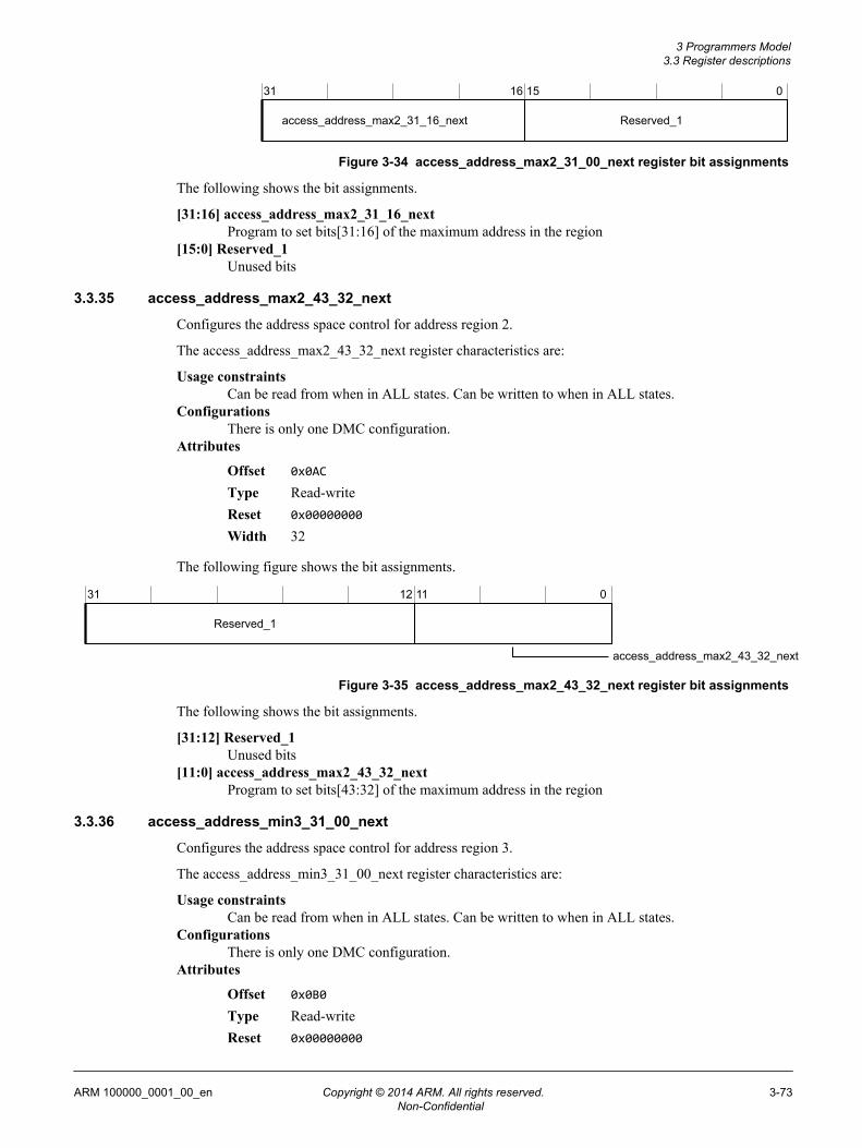
31 16 15 0
Reserved_1access_address_max2_31_16_next
Figure 3-34 access_address_max2_31_00_next register bit assignments
The following shows the bit assignments.
[31:16] access_address_max2_31_16_nextProgram to set bits[31:16] of the maximum address in the region
[15:0] Reserved_1Unused bits
3.3.35 access_address_max2_43_32_next
Configures the address space control for address region 2.
The access_address_max2_43_32_next register characteristics are:
Usage constraintsCan be read from when in ALL states. Can be written to when in ALL states.
ConfigurationsThere is only one DMC configuration.
Attributes
Offset 0x0AC
Type Read-writeReset 0x00000000
Width 32
The following figure shows the bit assignments.
31 12 11 0
Reserved_1
access_address_max2_43_32_next
Figure 3-35 access_address_max2_43_32_next register bit assignments
The following shows the bit assignments.
[31:12] Reserved_1Unused bits
[11:0] access_address_max2_43_32_nextProgram to set bits[43:32] of the maximum address in the region
3.3.36 access_address_min3_31_00_next
Configures the address space control for address region 3.
The access_address_min3_31_00_next register characteristics are:
Usage constraintsCan be read from when in ALL states. Can be written to when in ALL states.
ConfigurationsThere is only one DMC configuration.
Attributes
Offset 0x0B0
Type Read-writeReset 0x00000000
3 Programmers Model3.3 Register descriptions
ARM 100000_0001_00_en Copyright © 2014 ARM. All rights reserved. 3-73Non-Confidential

Width 32
The following figure shows the bit assignments.
31 16 15 4 3 2 1 0
Reserved_1access_address_min3_31_16_next
region_s_read_en3_nextregion_ns_write_en3_nextregion_ns_read_en3_next
region_s_write_en3_next
Figure 3-36 access_address_min3_31_00_next register bit assignments
The following shows the bit assignments.
[31:16] access_address_min3_31_16_nextProgram to set bits[31:16] of the minimum address in the region
[15:4] Reserved_1Unused bits
[3] region_s_write_en3_nextEnables Secure writes to the region
[2] region_s_read_en3_nextEnables Secure reads to the region
[1] region_ns_write_en3_nextEnables Non-secure writes to the region
[0] region_ns_read_en3_nextEnables Non-secure reads to the region
3.3.37 access_address_min3_43_32_next
Configures the address space control for address region 3.
The access_address_min3_43_32_next register characteristics are:
Usage constraintsCan be read from when in ALL states. Can be written to when in ALL states.
ConfigurationsThere is only one DMC configuration.
Attributes
Offset 0x0B4
Type Read-writeReset 0x00000000
Width 32
The following figure shows the bit assignments.
31 12 11 0
Reserved_1
access_address_min3_43_32_next
Figure 3-37 access_address_min3_43_32_next register bit assignments
The following shows the bit assignments.
[31:12] Reserved_1Unused bits
[11:0] access_address_min3_43_32_nextProgram to set bits[43:32] of the minimum address in the region
3 Programmers Model3.3 Register descriptions
ARM 100000_0001_00_en Copyright © 2014 ARM. All rights reserved. 3-74Non-Confidential

3.3.38 access_address_max3_31_00_next
Configures the address space control for address region 3.
The access_address_max3_31_00_next register characteristics are:
Usage constraintsCan be read from when in ALL states. Can be written to when in ALL states.
ConfigurationsThere is only one DMC configuration.
Attributes
Offset 0x0B8
Type Read-writeReset 0x00000000
Width 32
The following figure shows the bit assignments.
31 16 15 0
Reserved_1access_address_max3_31_16_next
Figure 3-38 access_address_max3_31_00_next register bit assignments
The following shows the bit assignments.
[31:16] access_address_max3_31_16_nextProgram to set bits[31:16] of the maximum address in the region
[15:0] Reserved_1Unused bits
3.3.39 access_address_max3_43_32_next
Configures the address space control for address region 3.
The access_address_max3_43_32_next register characteristics are:
Usage constraintsCan be read from when in ALL states. Can be written to when in ALL states.
ConfigurationsThere is only one DMC configuration.
Attributes
Offset 0x0BC
Type Read-writeReset 0x00000000
Width 32
The following figure shows the bit assignments.
31 12 11 0
Reserved_1
access_address_max3_43_32_next
Figure 3-39 access_address_max3_43_32_next register bit assignments
The following shows the bit assignments.
[31:12] Reserved_1Unused bits
3 Programmers Model3.3 Register descriptions
ARM 100000_0001_00_en Copyright © 2014 ARM. All rights reserved. 3-75Non-Confidential

[11:0] access_address_max3_43_32_nextProgram to set bits[43:32] of the maximum address in the region
3.3.40 access_address_min4_31_00_next
Configures the address space control for address region 4.
The access_address_min4_31_00_next register characteristics are:
Usage constraintsCan be read from when in ALL states. Can be written to when in ALL states.
ConfigurationsThere is only one DMC configuration.
Attributes
Offset 0x0C0
Type Read-writeReset 0x00000000
Width 32
The following figure shows the bit assignments.
31 16 15 4 3 2 1 0
Reserved_1access_address_min4_31_16_next
region_s_read_en4_nextregion_ns_write_en4_nextregion_ns_read_en4_next
region_s_write_en4_next
Figure 3-40 access_address_min4_31_00_next register bit assignments
The following shows the bit assignments.
[31:16] access_address_min4_31_16_nextProgram to set bits[31:16] of the minimum address in the region
[15:4] Reserved_1Unused bits
[3] region_s_write_en4_nextEnables Secure writes to the region
[2] region_s_read_en4_nextEnables Secure reads to the region
[1] region_ns_write_en4_nextEnables Non-secure writes to the region
[0] region_ns_read_en4_nextEnables Non-secure reads to the region
3.3.41 access_address_min4_43_32_next
Configures the address space control for address region 4.
The access_address_min4_43_32_next register characteristics are:
Usage constraintsCan be read from when in ALL states. Can be written to when in ALL states.
ConfigurationsThere is only one DMC configuration.
Attributes
Offset 0x0C4
Type Read-write
3 Programmers Model3.3 Register descriptions
ARM 100000_0001_00_en Copyright © 2014 ARM. All rights reserved. 3-76Non-Confidential

Reset 0x00000000
Width 32
The following figure shows the bit assignments.
31 12 11 0
Reserved_1
access_address_min4_43_32_next
Figure 3-41 access_address_min4_43_32_next register bit assignments
The following shows the bit assignments.
[31:12] Reserved_1Unused bits
[11:0] access_address_min4_43_32_nextProgram to set bits[43:32] of the minimum address in the region
3.3.42 access_address_max4_31_00_next
Configures the address space control for address region 4.
The access_address_max4_31_00_next register characteristics are:
Usage constraintsCan be read from when in ALL states. Can be written to when in ALL states.
ConfigurationsThere is only one DMC configuration.
Attributes
Offset 0x0C8
Type Read-writeReset 0x00000000
Width 32
The following figure shows the bit assignments.
31 16 15 0
Reserved_1access_address_max4_31_16_next
Figure 3-42 access_address_max4_31_00_next register bit assignments
The following shows the bit assignments.
[31:16] access_address_max4_31_16_nextProgram to set bits[31:16] of the maximum address in the region
[15:0] Reserved_1Unused bits
3.3.43 access_address_max4_43_32_next
Configures the address space control for address region 4.
The access_address_max4_43_32_next register characteristics are:
Usage constraintsCan be read from when in ALL states. Can be written to when in ALL states.
ConfigurationsThere is only one DMC configuration.
Attributes
3 Programmers Model3.3 Register descriptions
ARM 100000_0001_00_en Copyright © 2014 ARM. All rights reserved. 3-77Non-Confidential

Offset 0x0CC
Type Read-writeReset 0x00000000
Width 32
The following figure shows the bit assignments.
31 12 11 0
Reserved_1
access_address_max4_43_32_next
Figure 3-43 access_address_max4_43_32_next register bit assignments
The following shows the bit assignments.
[31:12] Reserved_1Unused bits
[11:0] access_address_max4_43_32_nextProgram to set bits[43:32] of the maximum address in the region
3.3.44 access_address_min5_31_00_next
Configures the address space control for address region 5.
The access_address_min5_31_00_next register characteristics are:
Usage constraintsCan be read from when in ALL states. Can be written to when in ALL states.
ConfigurationsThere is only one DMC configuration.
Attributes
Offset 0x0D0
Type Read-writeReset 0x00000000
Width 32
The following figure shows the bit assignments.
31 16 15 4 3 2 1 0
Reserved_1access_address_min5_31_16_next
region_s_read_en5_nextregion_ns_write_en5_nextregion_ns_read_en5_next
region_s_write_en5_next
Figure 3-44 access_address_min5_31_00_next register bit assignments
The following shows the bit assignments.
[31:16] access_address_min5_31_16_nextProgram to set bits[31:16] of the minimum address in the region
[15:4] Reserved_1Unused bits
[3] region_s_write_en5_nextEnables Secure writes to the region
[2] region_s_read_en5_nextEnables Secure reads to the region
3 Programmers Model3.3 Register descriptions
ARM 100000_0001_00_en Copyright © 2014 ARM. All rights reserved. 3-78Non-Confidential
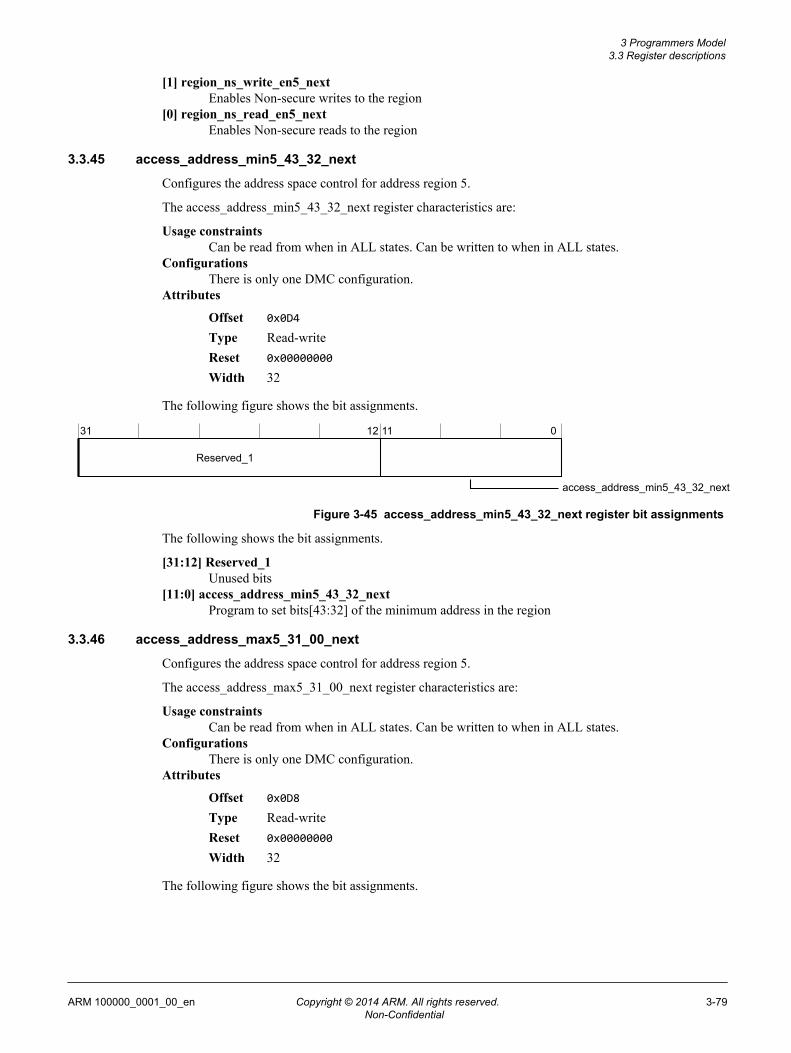
[1] region_ns_write_en5_nextEnables Non-secure writes to the region
[0] region_ns_read_en5_nextEnables Non-secure reads to the region
3.3.45 access_address_min5_43_32_next
Configures the address space control for address region 5.
The access_address_min5_43_32_next register characteristics are:
Usage constraintsCan be read from when in ALL states. Can be written to when in ALL states.
ConfigurationsThere is only one DMC configuration.
Attributes
Offset 0x0D4
Type Read-writeReset 0x00000000
Width 32
The following figure shows the bit assignments.
31 12 11 0
Reserved_1
access_address_min5_43_32_next
Figure 3-45 access_address_min5_43_32_next register bit assignments
The following shows the bit assignments.
[31:12] Reserved_1Unused bits
[11:0] access_address_min5_43_32_nextProgram to set bits[43:32] of the minimum address in the region
3.3.46 access_address_max5_31_00_next
Configures the address space control for address region 5.
The access_address_max5_31_00_next register characteristics are:
Usage constraintsCan be read from when in ALL states. Can be written to when in ALL states.
ConfigurationsThere is only one DMC configuration.
Attributes
Offset 0x0D8
Type Read-writeReset 0x00000000
Width 32
The following figure shows the bit assignments.
3 Programmers Model3.3 Register descriptions
ARM 100000_0001_00_en Copyright © 2014 ARM. All rights reserved. 3-79Non-Confidential

31 16 15 0
Reserved_1access_address_max5_31_16_next
Figure 3-46 access_address_max5_31_00_next register bit assignments
The following shows the bit assignments.
[31:16] access_address_max5_31_16_nextProgram to set bits[31:16] of the maximum address in the region
[15:0] Reserved_1Unused bits
3.3.47 access_address_max5_43_32_next
Configures the address space control for address region 5.
The access_address_max5_43_32_next register characteristics are:
Usage constraintsCan be read from when in ALL states. Can be written to when in ALL states.
ConfigurationsThere is only one DMC configuration.
Attributes
Offset 0x0DC
Type Read-writeReset 0x00000000
Width 32
The following figure shows the bit assignments.
31 12 11 0
Reserved_1
access_address_max5_43_32_next
Figure 3-47 access_address_max5_43_32_next register bit assignments
The following shows the bit assignments.
[31:12] Reserved_1Unused bits
[11:0] access_address_max5_43_32_nextProgram to set bits[43:32] of the maximum address in the region
3.3.48 access_address_min6_31_00_next
Configures the address space control for address region 6.
The access_address_min6_31_00_next register characteristics are:
Usage constraintsCan be read from when in ALL states. Can be written to when in ALL states.
ConfigurationsThere is only one DMC configuration.
Attributes
Offset 0x0E0
Type Read-writeReset 0x00000000
3 Programmers Model3.3 Register descriptions
ARM 100000_0001_00_en Copyright © 2014 ARM. All rights reserved. 3-80Non-Confidential

Width 32
The following figure shows the bit assignments.
31 16 15 4 3 2 1 0
Reserved_1access_address_min6_31_16_next
region_s_read_en6_nextregion_ns_write_en6_nextregion_ns_read_en6_next
region_s_write_en6_next
Figure 3-48 access_address_min6_31_00_next register bit assignments
The following shows the bit assignments.
[31:16] access_address_min6_31_16_nextProgram to set bits[31:16] of the minimum address in the region
[15:4] Reserved_1Unused bits
[3] region_s_write_en6_nextEnables Secure writes to the region
[2] region_s_read_en6_nextEnables Secure reads to the region
[1] region_ns_write_en6_nextEnables Non-secure writes to the region
[0] region_ns_read_en6_nextEnables Non-secure reads to the region
3.3.49 access_address_min6_43_32_next
Configures the address space control for address region 6.
The access_address_min6_43_32_next register characteristics are:
Usage constraintsCan be read from when in ALL states. Can be written to when in ALL states.
ConfigurationsThere is only one DMC configuration.
Attributes
Offset 0x0E4
Type Read-writeReset 0x00000000
Width 32
The following figure shows the bit assignments.
31 12 11 0
Reserved_1
access_address_min6_43_32_next
Figure 3-49 access_address_min6_43_32_next register bit assignments
The following shows the bit assignments.
[31:12] Reserved_1Unused bits
[11:0] access_address_min6_43_32_nextProgram to set bits[43:32] of the minimum address in the region
3 Programmers Model3.3 Register descriptions
ARM 100000_0001_00_en Copyright © 2014 ARM. All rights reserved. 3-81Non-Confidential

3.3.50 access_address_max6_31_00_next
Configures the address space control for address region 6.
The access_address_max6_31_00_next register characteristics are:
Usage constraintsCan be read from when in ALL states. Can be written to when in ALL states.
ConfigurationsThere is only one DMC configuration.
Attributes
Offset 0x0E8
Type Read-writeReset 0x00000000
Width 32
The following figure shows the bit assignments.
31 16 15 0
Reserved_1access_address_max6_31_16_next
Figure 3-50 access_address_max6_31_00_next register bit assignments
The following shows the bit assignments.
[31:16] access_address_max6_31_16_nextProgram to set bits[31:16] of the maximum address in the region
[15:0] Reserved_1Unused bits
3.3.51 access_address_max6_43_32_next
Configures the address space control for address region 6.
The access_address_max6_43_32_next register characteristics are:
Usage constraintsCan be read from when in ALL states. Can be written to when in ALL states.
ConfigurationsThere is only one DMC configuration.
Attributes
Offset 0x0EC
Type Read-writeReset 0x00000000
Width 32
The following figure shows the bit assignments.
31 12 11 0
Reserved_1
access_address_max6_43_32_next
Figure 3-51 access_address_max6_43_32_next register bit assignments
The following shows the bit assignments.
[31:12] Reserved_1Unused bits
3 Programmers Model3.3 Register descriptions
ARM 100000_0001_00_en Copyright © 2014 ARM. All rights reserved. 3-82Non-Confidential
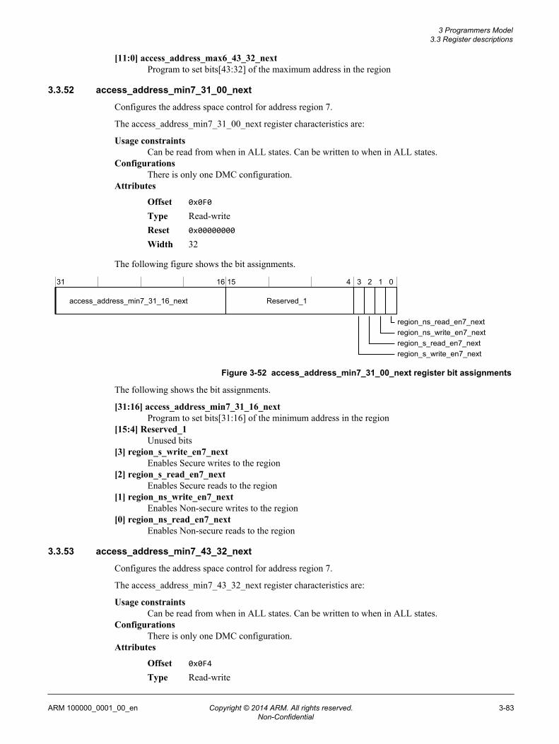
[11:0] access_address_max6_43_32_nextProgram to set bits[43:32] of the maximum address in the region
3.3.52 access_address_min7_31_00_next
Configures the address space control for address region 7.
The access_address_min7_31_00_next register characteristics are:
Usage constraintsCan be read from when in ALL states. Can be written to when in ALL states.
ConfigurationsThere is only one DMC configuration.
Attributes
Offset 0x0F0
Type Read-writeReset 0x00000000
Width 32
The following figure shows the bit assignments.
31 16 15 4 3 2 1 0
Reserved_1access_address_min7_31_16_next
region_s_read_en7_nextregion_ns_write_en7_nextregion_ns_read_en7_next
region_s_write_en7_next
Figure 3-52 access_address_min7_31_00_next register bit assignments
The following shows the bit assignments.
[31:16] access_address_min7_31_16_nextProgram to set bits[31:16] of the minimum address in the region
[15:4] Reserved_1Unused bits
[3] region_s_write_en7_nextEnables Secure writes to the region
[2] region_s_read_en7_nextEnables Secure reads to the region
[1] region_ns_write_en7_nextEnables Non-secure writes to the region
[0] region_ns_read_en7_nextEnables Non-secure reads to the region
3.3.53 access_address_min7_43_32_next
Configures the address space control for address region 7.
The access_address_min7_43_32_next register characteristics are:
Usage constraintsCan be read from when in ALL states. Can be written to when in ALL states.
ConfigurationsThere is only one DMC configuration.
Attributes
Offset 0x0F4
Type Read-write
3 Programmers Model3.3 Register descriptions
ARM 100000_0001_00_en Copyright © 2014 ARM. All rights reserved. 3-83Non-Confidential

Reset 0x00000000
Width 32
The following figure shows the bit assignments.
31 12 11 0
Reserved_1
access_address_min7_43_32_next
Figure 3-53 access_address_min7_43_32_next register bit assignments
The following shows the bit assignments.
[31:12] Reserved_1Unused bits
[11:0] access_address_min7_43_32_nextProgram to set bits[43:32] of the minimum address in the region
3.3.54 access_address_max7_31_00_next
Configures the address space control for address region 7.
The access_address_max7_31_00_next register characteristics are:
Usage constraintsCan be read from when in ALL states. Can be written to when in ALL states.
ConfigurationsThere is only one DMC configuration.
Attributes
Offset 0x0F8
Type Read-writeReset 0x00000000
Width 32
The following figure shows the bit assignments.
31 16 15 0
Reserved_1access_address_max7_31_16_next
Figure 3-54 access_address_max7_31_00_next register bit assignments
The following shows the bit assignments.
[31:16] access_address_max7_31_16_nextProgram to set bits[31:16] of the maximum address in the region
[15:0] Reserved_1Unused bits
3.3.55 access_address_max7_43_32_next
Configures the address space control for the address region 7.
The access_address_max7_43_32_next register characteristics are:
Usage constraintsCan be read from when in ALL states. Can be written to when in ALL states.
ConfigurationsThere is only one DMC configuration.
Attributes
3 Programmers Model3.3 Register descriptions
ARM 100000_0001_00_en Copyright © 2014 ARM. All rights reserved. 3-84Non-Confidential

Offset 0x0FC
Type Read-writeReset 0x00000000
Width 32
The following figure shows the bit assignments.
31 12 11 0
Reserved_1
access_address_max7_43_32_next
Figure 3-55 access_address_max7_43_32_next register bit assignments
The following shows the bit assignments.
[31:12] Reserved_1Unused bits
[11:0] access_address_max7_43_32_nextProgram to set bits[43:32] of the maximum address in the region
3.3.56 channel_status
Holds the current status of the memory channel.
The channel_status register characteristics are:
Usage constraintsCan be read from when in ALL states. Cannot be changed.
ConfigurationsThere is only one DMC configuration.
Attributes
Offset 0x100
Type Read-onlyReset 0x00000003
Width 32
The following figure shows the bit assignments.
31 30 29 28 27 26 25 24 23 22 21 20 19 18 17 16 15 8 7 3 2 1 0
Reserved_1m0_rank_sref
m0_low_powerm0_emptym0_idle
m0_rank_mrs_mode_cs0m0_rank_mrs_mode_cs1
m0_rank_mrs_mode_cs4m0_rank_mrs_mode_cs3m0_rank_mrs_mode_cs2
m0_rank_mrs_mode_cs7m0_rank_mrs_mode_cs6m0_rank_mrs_mode_cs5
Figure 3-56 channel_status register bit assignments
The following shows the bit assignments.
3 Programmers Model3.3 Register descriptions
ARM 100000_0001_00_en Copyright © 2014 ARM. All rights reserved. 3-85Non-Confidential
[31:30] m0_rank_mrs_mode_cs7m0_rank_mrs_mode_cs7 bitfield.
[29:28] m0_rank_mrs_mode_cs6m0_rank_mrs_mode_cs6 bitfield.
[27:26] m0_rank_mrs_mode_cs5m0_rank_mrs_mode_cs5 bitfield.
[25:24] m0_rank_mrs_mode_cs4m0_rank_mrs_mode_cs4 bitfield.
[23:22] m0_rank_mrs_mode_cs3m0_rank_mrs_mode_cs3 bitfield.
[21:20] m0_rank_mrs_mode_cs2m0_rank_mrs_mode_cs2 bitfield.
[19:18] m0_rank_mrs_mode_cs1m0_rank_mrs_mode_cs1 bitfield.
[17:16] m0_rank_mrs_mode_cs0Holds state information for this rank.
[15:8] m0_rank_srefOne-bit per rank indicating that the rank does not require the DMC to issue AUTOREFRESHcommands
[7:3] Reserved_1Unused bits
[2] m0_low_powerIndicates if all the DRAM ranks on this channel are in a state not requiring AUTOREFRESHcommands
[1] m0_emptyIndicates if the interface is empty, that is, there are no outstanding requests.
Note
This value might go non-empty at any time when in the READY state.
[0] m0_idleIndicates if the interface is idle, that is, there are no outstanding requests and no outstandingactivity, including delays, associated with previous commands.
Note
This value might go non-idle at any time when in the READY state.
3.3.57 direct_addr
Sets the direct command address field for direct commands.
The direct_addr register characteristics are:
Usage constraintsCan be read from when in ALL states. Can be written to when in CONFIG, PAUSED orREADY states.
ConfigurationsThere is only one DMC configuration.
Attributes
Offset 0x108
Type Read-writeReset 0x00000000
Width 32
The following figure shows the bit assignments.
3 Programmers Model3.3 Register descriptions
ARM 100000_0001_00_en Copyright © 2014 ARM. All rights reserved. 3-86Non-Confidential

31 0
direct_addr
Figure 3-57 direct_addr register bit assignments
The following shows the bit assignments.
[31:0] direct_addrFor more information see direct_cmd command descriptions.
3.3.58 direct_cmd
Generates direct commands from the manager.
The direct_cmd register characteristics are:
Usage constraintsCannot be read from. Can be written to when in CONFIG, PAUSED or READY states.
ConfigurationsThere is only one DMC configuration.
Attributes
Offset 0x10C
Type Write-onlyReset 0x00000000
Width 32
The following figure shows the bit assignments.
31 30 29 28 27 24 23 16 15 12 11 8 7 4 3 0
direct_barank_addr
Reserved_2Reserved_1direct_cmd
Reserved_3replay_overrideReserved_4
Figure 3-58 direct_cmd register bit assignments
The following shows the bit assignments.
[31:30] Reserved_4Unused bits
[29:28] replay_overrideDefines the replay behavior for this particular command.
[27:24] Reserved_3Unused bits
[23:16] rank_addrDetermines the target rank, each bit corresponding to a rank. If multiple ranks are selected thenthe command is sent to each rank in turn.
[15:12] Reserved_2Unused bits
[11:8] direct_baDetermines the value to be driven on the external bank group and bank address pins. For MRScommands, it is the mode register number. For all other commands, bank group (ifprogrammed) is taken from the least significant bits, bank address is taken from the bits directlyabove the bank group bits.
3 Programmers Model3.3 Register descriptions
ARM 100000_0001_00_en Copyright © 2014 ARM. All rights reserved. 3-87Non-Confidential

[7:4] Reserved_1Unused bits
[3:0] direct_cmdDetermines the command to be performed.
3.3.59 dci_replay_type_next
Configures the behavior of the DMC if a DRAM or PHY error is received when executing a directcommand.
The dci_replay_type_next register characteristics are:
Usage constraintsCan be read from when in ALL states. Can be written to when in ALL states.
ConfigurationsThere is only one DMC configuration.
Attributes
Offset 0x110
Type Read-writeReset 0x00000002
Width 32
The following figure shows the bit assignments.
31 2 1 0
Reserved_1
dci_replay_type_next
Figure 3-59 dci_replay_type_next register bit assignments
The following shows the bit assignments.
[31:2] Reserved_1Unused bits
[1:0] dci_replay_type_nextdci_replay_type_next bitfield.
3.3.60 dci_strb
Configures the write data strobe values used during direct_cmd WRITE operations.
The dci_strb register characteristics are:
Usage constraintsCan be read from when in ALL states. Can be written to when in CONFIG, PAUSED orREADY states.
ConfigurationsThere is only one DMC configuration.
Attributes
Offset 0x118
Type Read-writeReset 0x0000000F
Width 32
The following figure shows the bit assignments.
3 Programmers Model3.3 Register descriptions
ARM 100000_0001_00_en Copyright © 2014 ARM. All rights reserved. 3-88Non-Confidential

31 4 3 0
dci_strbReserved_1
Figure 3-60 dci_strb register bit assignments
The following shows the bit assignments.
[31:4] Reserved_1Unused bits
[3:0] dci_strbFor write operations, provides the value used to drive DQM, where a value of 1 indicates datamust be committed to DRAM. You must write once for each 32-bit data word to write as part ofa DRAM burst. Defaults to 4'b1111.
3.3.61 dci_data
Reading from this register location returns read data received a result of a READ command. Writing tothis register location sets the data to be used for direct_cmd WRITE commands. You must read or writeonce for each 32-bit data word of a DRAM burst.
The dci_data register characteristics are:
Usage constraintsCan be read from when in CONFIG, PAUSED or READY states. Can be written to when inCONFIG, PAUSED or READY states.
ConfigurationsThere is only one DMC configuration.
Attributes
Offset 0x11C
Type Read-writeReset 0x00000000
Width 32
The following figure shows the bit assignments.
31 0
dci_data
Figure 3-61 dci_data register bit assignments
The following shows the bit assignments.
[31:0] dci_datadci_data bitfield.
3.3.62 refresh_control_next
Configures the type of refresh commands issued by the DMC.
The refresh_control_next register characteristics are:
Usage constraintsCan be read from when in ALL states. Can be written to when in ALL states.
ConfigurationsThere is only one DMC configuration.
Attributes
Offset 0x120
Type Read-write
3 Programmers Model3.3 Register descriptions
ARM 100000_0001_00_en Copyright © 2014 ARM. All rights reserved. 3-89Non-Confidential

Reset 0x00000000
Width 32
The following figure shows the bit assignments.
31 6 5 4 3 0
Reserved_2
refresh_granularity_nextReserved_1
Figure 3-62 refresh_control_next register bit assignments
The following shows the bit assignments.
[31:6] Reserved_2Unused bits
[5:4] refresh_granularity_nextConfigures the refresh rate mode of the DMC. You must program this to match the mode of theDRAM. All DRAMs requiring refresh must use the same refresh rate.
[3:0] Reserved_1Unused bits
3.3.63 memory_type_next
Configures the DMC for the attached memory type.
The memory_type_next register characteristics are:
Usage constraintsCan be read from when in ALL states. Can be written to when in ALL states.
ConfigurationsThere is only one DMC configuration.
Attributes
Offset 0x128
Type Read-writeReset 0x00000101
Width 32
The following figure shows the bit assignments.
31 18 17 16 15 10 9 8 7 6 5 4 3 2 0
Reserved_4Reserved_5
Reserved_2Reserved_1memory_type_next
Reserved_3memory_device_width_nextmemory_bank_groups_next
Figure 3-63 memory_type_next register bit assignments
The following shows the bit assignments.
[31:18] Reserved_5Unused bits
[17:16] memory_bank_groups_nextProgram to configure the number of bank groups in the attached memory device
3 Programmers Model3.3 Register descriptions
ARM 100000_0001_00_en Copyright © 2014 ARM. All rights reserved. 3-90Non-Confidential

[15:10] Reserved_4Unused bits
[9:8] memory_device_width_nextProgram to configure the device widths.
[7:6] Reserved_3Unused bits
[5:4] Reserved_2Unused bits
[3] Reserved_1Unused bits
[2:0] memory_type_nextProgram to configure the attached memory type
3.3.64 feature_config
Control register for DMC features.
The feature_config register characteristics are:
Usage constraintsCan be read from when in ALL states. Can be written to when in CONFIG or LOW-POWERstates.
ConfigurationsThere is only one DMC configuration.
Attributes
Offset 0x130
Type Read-writeReset 0x000000F0
Width 32
The following figure shows the bit assignments.
31 11 10 9 8 7 6 5 4 3 2 1 0
Reserved_1
uncorrected_retrycorrected_writebackecc_enable
rmw_enableclk_gate_en
si_clk_gate_disableparity_maskpmu_enable
mi_clk_gate_disabledcb_clk_gate_disable
Figure 3-64 feature_config register bit assignments
The following shows the bit assignments.
[31:11] Reserved_1Unused bits
[10] mi_clk_gate_disableDisable clock gating for the memory interface.
[9] dcb_clk_gate_disableDisable clock gating for the main DMC queue.
[8] si_clk_gate_disableDisable clock gating for the system interface.
3 Programmers Model3.3 Register descriptions
ARM 100000_0001_00_en Copyright © 2014 ARM. All rights reserved. 3-91Non-Confidential

[7] parity_maskProgram to include a[17] in parity calculation.
[6] pmu_enableEnable performance monitoring unit outputs.
[5] clk_gate_enEnable clock gating for DMC.
[4] rmw_enableEnable read-modify-write operations. Must be enabled if Write DBI or ECC is enabled.
[3] uncorrected_retryProgram to enable or disable retry of ECC-uncorrectable data operations.
[2] corrected_writebackProgram to enable or disable write-back of ECC-corrected data.
[1:0] ecc_enableProgram to enable or disable ECC functionality.
3.3.65 nibble_failed_031_000
Used to inform the DMC that a particular nibble has failed.
The nibble_failed_031_000 register characteristics are:
Usage constraintsCan be read from when in ALL states. Can be written to when in ALL states.
ConfigurationsThere is only one DMC configuration.
Attributes
Offset 0x138
Type Read-writeReset 0x00000000
Width 32
The following figure shows the bit assignments.
31 24 23 22 18 17 16 12 11 10 6 5 4 0
Reserved_1
nibble_failed_rank0_secondnibble_failed_rank0_first_validnibble_failed_rank0_first
nibble_failed_rank0_second_validnibble_failed_rank1_first
nibble_failed_rank1_second_validnibble_failed_rank1_secondnibble_failed_rank1_first_valid
Figure 3-65 nibble_failed_031_000 register bit assignments
The following shows the bit assignments.
[31:24] Reserved_1Unused bits
[23] nibble_failed_rank1_second_validIndicates if the second location is valid.
[22:18] nibble_failed_rank1_secondUsed to inform the DMC of the second location that has failed. The supported range for thisbitfield is 0-17.
[17] nibble_failed_rank1_first_validIndicates if the first location is valid.
3 Programmers Model3.3 Register descriptions
ARM 100000_0001_00_en Copyright © 2014 ARM. All rights reserved. 3-92Non-Confidential

[16:12] nibble_failed_rank1_firstUsed to inform the DMC of the first location that has failed. The supported range for thisbitfield is 0-17.
[11] nibble_failed_rank0_second_validIndicates if the second location is valid.
[10:6] nibble_failed_rank0_secondUsed to inform the DMC of the second location that has failed. The supported range for thisbitfield is 0-17.
[5] nibble_failed_rank0_first_validIndicates if the first location is valid.
[4:0] nibble_failed_rank0_firstUsed to inform the DMC of the first location that has failed. The supported range for thisbitfield is 0-17.
3.3.66 nibble_failed_063_032
Used to inform the DMC that a particular nibble has failed.
The nibble_failed_063_032 register characteristics are:
Usage constraintsCan be read from when in ALL states. Can be written to when in ALL states.
ConfigurationsThere is only one DMC configuration.
Attributes
Offset 0x13C
Type Read-writeReset 0x00000000
Width 32
The following figure shows the bit assignments.
31 24 23 22 18 17 16 12 11 10 6 5 4 0
Reserved_1
nibble_failed_rank2_secondnibble_failed_rank2_first_validnibble_failed_rank2_first
nibble_failed_rank2_second_validnibble_failed_rank3_first
nibble_failed_rank3_second_validnibble_failed_rank3_secondnibble_failed_rank3_first_valid
Figure 3-66 nibble_failed_063_032 register bit assignments
The following shows the bit assignments.
[31:24] Reserved_1Unused bits
[23] nibble_failed_rank3_second_validIndicates if the second location is valid.
[22:18] nibble_failed_rank3_secondUsed to inform the DMC of the second location that has failed. The supported range for thisbitfield is 0-17.
[17] nibble_failed_rank3_first_validIndicates if the first location is valid.
3 Programmers Model3.3 Register descriptions
ARM 100000_0001_00_en Copyright © 2014 ARM. All rights reserved. 3-93Non-Confidential

[16:12] nibble_failed_rank3_firstUsed to inform the DMC of the first location that has failed. The supported range for thisbitfield is 0-17.
[11] nibble_failed_rank2_second_validIndicates if the second location is valid.
[10:6] nibble_failed_rank2_secondUsed to inform the DMC of the second location that has failed. The supported range for thisbitfield is 0-17.
[5] nibble_failed_rank2_first_validIndicates if the first location is valid.
[4:0] nibble_failed_rank2_firstUsed to inform the DMC of the first location that has failed. The supported range for thisbitfield is 0-17.
3.3.67 nibble_failed_095_064
Used to inform the DMC that a particular nibble has failed.
The nibble_failed_095_064 register characteristics are:
Usage constraintsCan be read from when in ALL states. Can be written to when in ALL states.
ConfigurationsThere is only one DMC configuration.
Attributes
Offset 0x140
Type Read-writeReset 0x00000000
Width 32
The following figure shows the bit assignments.
31 24 23 22 18 17 16 12 11 10 6 5 4 0
Reserved_1
nibble_failed_rank4_secondnibble_failed_rank4_first_validnibble_failed_rank4_first
nibble_failed_rank4_second_validnibble_failed_rank5_first
nibble_failed_rank5_second_validnibble_failed_rank5_secondnibble_failed_rank5_first_valid
Figure 3-67 nibble_failed_095_064 register bit assignments
The following shows the bit assignments.
[31:24] Reserved_1Unused bits
[23] nibble_failed_rank5_second_validIndicates if the second location is valid.
[22:18] nibble_failed_rank5_secondUsed to inform the DMC of the second location that has failed. The supported range for thisbitfield is 0-17.
[17] nibble_failed_rank5_first_validIndicates if the first location is valid.
3 Programmers Model3.3 Register descriptions
ARM 100000_0001_00_en Copyright © 2014 ARM. All rights reserved. 3-94Non-Confidential

[16:12] nibble_failed_rank5_firstUsed to inform the DMC of the first location that has failed. The supported range for thisbitfield is 0-17.
[11] nibble_failed_rank4_second_validIndicates if the second location is valid.
[10:6] nibble_failed_rank4_secondUsed to inform the DMC of the second location that has failed. The supported range for thisbitfield is 0-17.
[5] nibble_failed_rank4_first_validIndicates if the first location is valid.
[4:0] nibble_failed_rank4_firstUsed to inform the DMC of the first location that has failed. The supported range for thisbitfield is 0-17.
3.3.68 nibble_failed_127_096
Used to inform the DMC that a particular nibble has failed.
The nibble_failed_127_096 register characteristics are:
Usage constraintsCan be read from when in ALL states. Can be written to when in ALL states.
ConfigurationsThere is only one DMC configuration.
Attributes
Offset 0x144
Type Read-writeReset 0x00000000
Width 32
The following figure shows the bit assignments.
31 24 23 22 18 17 16 12 11 10 6 5 4 0
Reserved_1
nibble_failed_rank6_secondnibble_failed_rank6_first_validnibble_failed_rank6_first
nibble_failed_rank6_second_validnibble_failed_rank7_first
nibble_failed_rank7_second_validnibble_failed_rank7_secondnibble_failed_rank7_first_valid
Figure 3-68 nibble_failed_127_096 register bit assignments
The following shows the bit assignments.
[31:24] Reserved_1Unused bits
[23] nibble_failed_rank7_second_validIndicates if the second location is valid.
[22:18] nibble_failed_rank7_secondUsed to inform the DMC of the second location that has failed. The supported range for thisbitfield is 0-17.
[17] nibble_failed_rank7_first_validIndicates if the first location is valid.
3 Programmers Model3.3 Register descriptions
ARM 100000_0001_00_en Copyright © 2014 ARM. All rights reserved. 3-95Non-Confidential

[16:12] nibble_failed_rank7_firstUsed to inform the DMC of the first location that has failed. The supported range for thisbitfield is 0-17.
[11] nibble_failed_rank6_second_validIndicates if the second location is valid.
[10:6] nibble_failed_rank6_secondUsed to inform the DMC of the second location that has failed. The supported range for thisbitfield is 0-17.
[5] nibble_failed_rank6_first_validIndicates if the first location is valid.
[4:0] nibble_failed_rank6_firstUsed to inform the DMC of the first location that has failed. The supported range for thisbitfield is 0-17.
3.3.69 queue_allocate_control_031_000
Used to inform the DMC that a particular queue (RAM) entry has failed, where 0 means failed and notincluded for allocation.
The queue_allocate_control_031_000 register characteristics are:
Usage constraintsCan be read from when in ALL states. Can be written to when in ALL states.
ConfigurationsThere is only one DMC configuration.
Attributes
Offset 0x148
Type Read-writeReset 0xFFFFFFFF
Width 32
The following figure shows the bit assignments.
31 0
queue_allocate_control_031_000
Figure 3-69 queue_allocate_control_031_000 register bit assignments
The following shows the bit assignments.
[31:0] queue_allocate_control_031_000Used to inform the DMC that a particular queue (RAM) entry has failed, where 0 means failedand not included for allocation.
3.3.70 queue_allocate_control_063_032
Configures the DMC to not allocate particular queue entries (one bit per entry), for example to avoidusing faulty internal RAM locations.
The queue_allocate_control_063_032 register characteristics are:
Usage constraintsCan be read from when in ALL states. Can be written to when in ALL states.
ConfigurationsThere is only one DMC configuration.
Attributes
Offset 0x14C
Type Read-write
3 Programmers Model3.3 Register descriptions
ARM 100000_0001_00_en Copyright © 2014 ARM. All rights reserved. 3-96Non-Confidential

Reset 0xFFFFFFFF
Width 32
The following figure shows the bit assignments.
31 0
queue_allocate_control_063_032
Figure 3-70 queue_allocate_control_063_032 register bit assignments
The following shows the bit assignments.
[31:0] queue_allocate_control_063_032queue_allocate_control_063_032 bitfield.
3.3.71 queue_allocate_control_095_064
Configures the DMC to not allocate particular queue entries (one bit per entry), for example to avoidusing faulty internal RAM locations.
The queue_allocate_control_095_064 register characteristics are:
Usage constraintsCan be read from when in ALL states. Can be written to when in ALL states.
ConfigurationsThere is only one DMC configuration.
Attributes
Offset 0x150
Type Read-writeReset 0xFFFFFFFF
Width 32
The following figure shows the bit assignments.
31 0
queue_allocate_control_095_064
Figure 3-71 queue_allocate_control_095_064 register bit assignments
The following shows the bit assignments.
[31:0] queue_allocate_control_095_064queue_allocate_control_095_064 bitfield.
3.3.72 queue_allocate_control_127_096
Configures the DMC to not allocate particular queue entries (one bit per entry), for example to avoidusing faulty internal RAM locations.
The queue_allocate_control_127_096 register characteristics are:
Usage constraintsCan be read from when in ALL states. Can be written to when in ALL states.
ConfigurationsThere is only one DMC configuration.
Attributes
Offset 0x154
Type Read-write
3 Programmers Model3.3 Register descriptions
ARM 100000_0001_00_en Copyright © 2014 ARM. All rights reserved. 3-97Non-Confidential

Reset 0xFFFFFFFF
Width 32
The following figure shows the bit assignments.
31 0
queue_allocate_control_127_096
Figure 3-72 queue_allocate_control_127_096 register bit assignments
The following shows the bit assignments.
[31:0] queue_allocate_control_127_096queue_allocate_control_127_096 bitfield.
3.3.73 ecc_errc_count_31_00
Counter register for the DRAM ECC functionality.
The ecc_errc_count_31_00 register characteristics are:
Usage constraintsCan be read from when in ALL states. Can be written to when in ALL states.
ConfigurationsThere is only one DMC configuration.
Attributes
Offset 0x158
Type Read-writeReset 0x00000000
Width 32
The following figure shows the bit assignments.
31 24 23 16 15 8 7 0
rank0_errc_countrank1_errc_countrank2_errc_countrank3_errc_count
Figure 3-73 ecc_errc_count_31_00 register bit assignments
The following shows the bit assignments.
[31:24] rank3_errc_countCorrected error count. A write to the bitfield resets the counter to the written value.
[23:16] rank2_errc_countCorrected error count. A write to the bitfield resets the counter to the written value.
[15:8] rank1_errc_countCorrected error count. A write to the bitfield resets the counter to the written value.
[7:0] rank0_errc_countCorrected error count. A write to the bitfield resets the counter to the written value.
3.3.74 ecc_errc_count_63_32
Counter register for the DRAM ECC functionality.
The ecc_errc_count_63_32 register characteristics are:
Usage constraintsCan be read from when in ALL states. Can be written to when in ALL states.
ConfigurationsThere is only one DMC configuration.
3 Programmers Model3.3 Register descriptions
ARM 100000_0001_00_en Copyright © 2014 ARM. All rights reserved. 3-98Non-Confidential

Attributes
Offset 0x15C
Type Read-writeReset 0x00000000
Width 32
The following figure shows the bit assignments.
31 24 23 16 15 8 7 0
rank4_errc_countrank5_errc_countrank6_errc_countrank7_errc_count
Figure 3-74 ecc_errc_count_63_32 register bit assignments
The following shows the bit assignments.
[31:24] rank7_errc_countCorrected error count. A write to the bitfield resets the counter to the written value.
[23:16] rank6_errc_countCorrected error count. A write to the bitfield resets the counter to the written value.
[15:8] rank5_errc_countCorrected error count. A write to the bitfield resets the counter to the written value.
[7:0] rank4_errc_countCorrected error count. A write to the bitfield resets the counter to the written value.
3.3.75 ecc_errd_count_31_00
Counter register for the DRAM ECC functionality.
The ecc_errd_count_31_00 register characteristics are:
Usage constraintsCan be read from when in ALL states. Can be written to when in ALL states.
ConfigurationsThere is only one DMC configuration.
Attributes
Offset 0x160
Type Read-writeReset 0x00000000
Width 32
The following figure shows the bit assignments.
31 24 23 16 15 8 7 0
rank0_errd_countrank1_errd_countrank2_errd_countrank3_errd_count
Figure 3-75 ecc_errd_count_31_00 register bit assignments
The following shows the bit assignments.
[31:24] rank3_errd_countUncorrected error count. A write to the bitfield resets the counter to the written value.
[23:16] rank2_errd_countUncorrected error count. A write to the bitfield resets the counter to the written value.
[15:8] rank1_errd_countUncorrected error count. A write to the bitfield resets the counter to the written value.
[7:0] rank0_errd_countUncorrected error count. A write to the bitfield resets the counter to the written value.
3 Programmers Model3.3 Register descriptions
ARM 100000_0001_00_en Copyright © 2014 ARM. All rights reserved. 3-99Non-Confidential
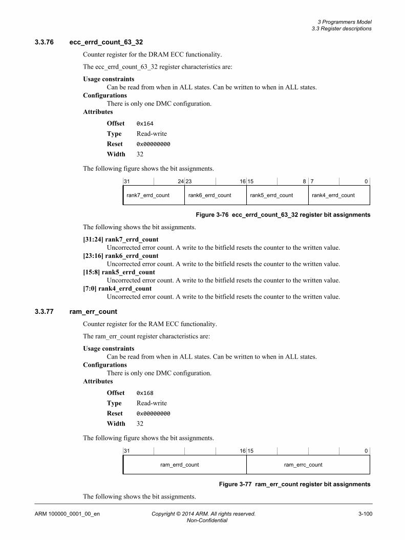
3.3.76 ecc_errd_count_63_32
Counter register for the DRAM ECC functionality.
The ecc_errd_count_63_32 register characteristics are:
Usage constraintsCan be read from when in ALL states. Can be written to when in ALL states.
ConfigurationsThere is only one DMC configuration.
Attributes
Offset 0x164
Type Read-writeReset 0x00000000
Width 32
The following figure shows the bit assignments.
31 24 23 16 15 8 7 0
rank4_errd_countrank5_errd_countrank6_errd_countrank7_errd_count
Figure 3-76 ecc_errd_count_63_32 register bit assignments
The following shows the bit assignments.
[31:24] rank7_errd_countUncorrected error count. A write to the bitfield resets the counter to the written value.
[23:16] rank6_errd_countUncorrected error count. A write to the bitfield resets the counter to the written value.
[15:8] rank5_errd_countUncorrected error count. A write to the bitfield resets the counter to the written value.
[7:0] rank4_errd_countUncorrected error count. A write to the bitfield resets the counter to the written value.
3.3.77 ram_err_count
Counter register for the RAM ECC functionality.
The ram_err_count register characteristics are:
Usage constraintsCan be read from when in ALL states. Can be written to when in ALL states.
ConfigurationsThere is only one DMC configuration.
Attributes
Offset 0x168
Type Read-writeReset 0x00000000
Width 32
The following figure shows the bit assignments.
31 16 15 0
ram_errc_countram_errd_count
Figure 3-77 ram_err_count register bit assignments
The following shows the bit assignments.
3 Programmers Model3.3 Register descriptions
ARM 100000_0001_00_en Copyright © 2014 ARM. All rights reserved. 3-100Non-Confidential
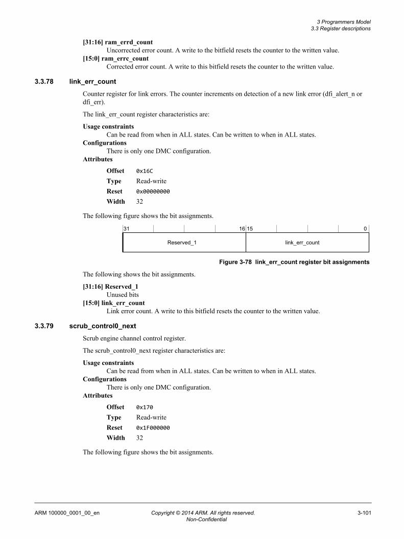
[31:16] ram_errd_countUncorrected error count. A write to the bitfield resets the counter to the written value.
[15:0] ram_errc_countCorrected error count. A write to this bitfield resets the counter to the written value.
3.3.78 link_err_count
Counter register for link errors. The counter increments on detection of a new link error (dfi_alert_n ordfi_err).
The link_err_count register characteristics are:
Usage constraintsCan be read from when in ALL states. Can be written to when in ALL states.
ConfigurationsThere is only one DMC configuration.
Attributes
Offset 0x16C
Type Read-writeReset 0x00000000
Width 32
The following figure shows the bit assignments.
31 16 15 0
link_err_countReserved_1
Figure 3-78 link_err_count register bit assignments
The following shows the bit assignments.
[31:16] Reserved_1Unused bits
[15:0] link_err_countLink error count. A write to this bitfield resets the counter to the written value.
3.3.79 scrub_control0_next
Scrub engine channel control register.
The scrub_control0_next register characteristics are:
Usage constraintsCan be read from when in ALL states. Can be written to when in ALL states.
ConfigurationsThere is only one DMC configuration.
Attributes
Offset 0x170
Type Read-writeReset 0x1F000000
Width 32
The following figure shows the bit assignments.
3 Programmers Model3.3 Register descriptions
ARM 100000_0001_00_en Copyright © 2014 ARM. All rights reserved. 3-101Non-Confidential

31 29 28 24 23 20 19 16 15 14 13 12 9 8 7 6 5 4 3 2 1 0
scrub_addr_mode0_nextReserved_1trigger0_next
Reserved_2completion_interrupt0_next
stop_on_page0_nextqos_for_scrub0_nextReserved_3
Reserved_5escalation_count_scrub0_nextReserved_4
outstanding_request_limit_scrub0_nextReserved_6
Figure 3-79 scrub_control0_next register bit assignments
The following shows the bit assignments.
[31:29] Reserved_6Unused bits
[28:24] outstanding_request_limit_scrub0_nextConfigures the maximum number of oustanding scrub requests for scrub program 0 Thesupported range for this bitfield is 8-31.
[23:20] Reserved_5Unused bits
[19:16] escalation_count_scrub0_nextConfigures number of escalation prescalar periods before incrementing priority for scruboperations (0 disables this feature)
[15:14] Reserved_4Unused bits
[13] stop_on_page0_nextConfigures stop_on_page of scrub operations, scrub program will pause when reach pageaddress if set
[12:9] qos_for_scrub0_nextConfigures QoS value of scrub operations
[8:7] Reserved_3Unused bits
[6] completion_interrupt0_nextConfigures whether to emit an event when the sequence completes
[5:4] Reserved_2Unused bits
[3] scrub_addr_mode0_nextConfigures scrub address mode
[2] Reserved_1Unused bits
[1:0] trigger0_nextControls the trigger event associated with the channel operation.
3.3.80 scrub_address_min0_next
Configures the address space control for the scrub engine channel.
The scrub_address_min0_next register characteristics are:
Usage constraintsCan be read from when in ALL states. Can be written to when in ALL states.
3 Programmers Model3.3 Register descriptions
ARM 100000_0001_00_en Copyright © 2014 ARM. All rights reserved. 3-102Non-Confidential
ConfigurationsThere is only one DMC configuration.
Attributes
Offset 0x174
Type Read-writeReset 0x00000000
Width 32
The following figure shows the bit assignments.
31 0
scrub_address_min0_next
Figure 3-80 scrub_address_min0_next register bit assignments
The following shows the bit assignments.
[31:0] scrub_address_min0_nextProgram to set the starting address for the scrub engine. When scrub_addr_mode0 is set tophysical_address this register specifies logical rank [24:22], physical bank [21:18] and physicalrow address [17:0] directly. When scrub_addr_mode0 is set to system_address this registerspecifies the address in the same address format used by incoming system transactions.
3.3.81 scrub_address_max0_next
Configures the address space control for the scrub engine channel.
The scrub_address_max0_next register characteristics are:
Usage constraintsCan be read from when in ALL states. Can be written to when in ALL states.
ConfigurationsThere is only one DMC configuration.
Attributes
Offset 0x178
Type Read-writeReset 0x00000000
Width 32
The following figure shows the bit assignments.
31 0
scrub_address_max0_next
Figure 3-81 scrub_address_max0_next register bit assignments
The following shows the bit assignments.
[31:0] scrub_address_max0_nextProgram to set the ending address for the scrub engine. When scrub_addr_mode0 is set tophysical_address this register specifies logical rank [24:22], physical bank [21:18] and physicalrow address [17:0] directly. When scrub_addr_mode0 is set to system_address this registerspecifies the address in the same address format used by incoming system transactions.
3 Programmers Model3.3 Register descriptions
ARM 100000_0001_00_en Copyright © 2014 ARM. All rights reserved. 3-103Non-Confidential

3.3.82 scrub_control1_next
Scrub engine channel control register.
The scrub_control1_next register characteristics are:
Usage constraintsCan be read from when in ALL states. Can be written to when in ALL states.
ConfigurationsThere is only one DMC configuration.
Attributes
Offset 0x180
Type Read-writeReset 0x1F000000
Width 32
The following figure shows the bit assignments.
31 29 28 24 23 20 19 16 15 14 13 12 9 8 7 6 5 4 3 2 1 0
scrub_addr_mode1_nextReserved_1trigger1_next
Reserved_2completion_interrupt1_next
stop_on_page1_nextqos_for_scrub1_nextReserved_3
Reserved_5escalation_count_scrub1_nextReserved_4
outstanding_request_limit_scrub1_nextReserved_6
Figure 3-82 scrub_control1_next register bit assignments
The following shows the bit assignments.
[31:29] Reserved_6Unused bits
[28:24] outstanding_request_limit_scrub1_nextConfigures the maximum number of oustanding scrub requests for scrub program 1 Thesupported range for this bitfield is 8-31.
[23:20] Reserved_5Unused bits
[19:16] escalation_count_scrub1_nextConfigures number of escalation prescalar periods before incrementing priority for scruboperations (0 disables this feature)
[15:14] Reserved_4Unused bits
[13] stop_on_page1_nextConfigures stop_on_page of scrub operations, scrub program will pause when reach pageaddress if set
[12:9] qos_for_scrub1_nextConfigures QoS value of scrub operations
[8:7] Reserved_3Unused bits
3 Programmers Model3.3 Register descriptions
ARM 100000_0001_00_en Copyright © 2014 ARM. All rights reserved. 3-104Non-Confidential

[6] completion_interrupt1_nextConfigures whether to emit an event when the sequence completes
[5:4] Reserved_2Unused bits
[3] scrub_addr_mode1_nextConfigures scrub address mode
[2] Reserved_1Unused bits
[1:0] trigger1_nextControls the trigger event associated with the channel operation.
3.3.83 scrub_address_min1_next
Configures the address space control for the scrub engine channel.
The scrub_address_min1_next register characteristics are:
Usage constraintsCan be read from when in ALL states. Can be written to when in ALL states.
ConfigurationsThere is only one DMC configuration.
Attributes
Offset 0x184
Type Read-writeReset 0x00000000
Width 32
The following figure shows the bit assignments.
31 0
scrub_address_min1_next
Figure 3-83 scrub_address_min1_next register bit assignments
The following shows the bit assignments.
[31:0] scrub_address_min1_nextProgram to set the starting address for the scrub engine. When scrub_addr_mode1 is set tophysical_address this register specifies logical rank [24:22], physical bank [21:18] and physicalrow address [17:0] directly. When scrub_addr_mode1 is set to system_address this registerspecifies the address in the same address format used by incoming system transactions.
3.3.84 scrub_address_max1_next
Configures the address space control for the scrub engine channel.
The scrub_address_max1_next register characteristics are:
Usage constraintsCan be read from when in ALL states. Can be written to when in ALL states.
ConfigurationsThere is only one DMC configuration.
Attributes
Offset 0x188
Type Read-writeReset 0x00000000
Width 32
3 Programmers Model3.3 Register descriptions
ARM 100000_0001_00_en Copyright © 2014 ARM. All rights reserved. 3-105Non-Confidential

The following figure shows the bit assignments.
31 0
scrub_address_max1_next
Figure 3-84 scrub_address_max1_next register bit assignments
The following shows the bit assignments.
[31:0] scrub_address_max1_nextProgram to set the ending address for the scrub engine. When scrub_addr_mode1 is set tophysical_address this register specifies logical rank [24:22], physical bank [21:18] and physicalrow address [17:0] directly. When scrub_addr_mode1 is set to system_address this registerspecifies the address in the same address format used by incoming system transactions.
3.3.85 scrub_control2_next
Scrub engine channel control register.
The scrub_control2_next register characteristics are:
Usage constraintsCan be read from when in ALL states. Can be written to when in ALL states.
ConfigurationsThere is only one DMC configuration.
Attributes
Offset 0x190
Type Read-writeReset 0x1F000000
Width 32
The following figure shows the bit assignments.
31 29 28 24 23 20 19 16 15 14 13 12 9 8 7 6 5 4 3 2 1 0
scrub_addr_mode2_nextReserved_1trigger2_next
Reserved_2completion_interrupt2_next
stop_on_page2_nextqos_for_scrub2_nextReserved_3
Reserved_5escalation_count_scrub2_nextReserved_4
outstanding_request_limit_scrub2_nextReserved_6
Figure 3-85 scrub_control2_next register bit assignments
The following shows the bit assignments.
[31:29] Reserved_6Unused bits
[28:24] outstanding_request_limit_scrub2_nextConfigures the maximum number of oustanding scrub requests for scrub program 2 Thesupported range for this bitfield is 8-31.
3 Programmers Model3.3 Register descriptions
ARM 100000_0001_00_en Copyright © 2014 ARM. All rights reserved. 3-106Non-Confidential

[23:20] Reserved_5Unused bits
[19:16] escalation_count_scrub2_nextConfigures number of escalation prescalar periods before incrementing priority for scruboperations (0 disables this feature)
[15:14] Reserved_4Unused bits
[13] stop_on_page2_nextConfigures stop_on_page of scrub operations, scrub program will pause when reach pageaddress if set
[12:9] qos_for_scrub2_nextConfigures QoS value of scrub operations
[8:7] Reserved_3Unused bits
[6] completion_interrupt2_nextConfigures whether to emit an event when the sequence completes
[5:4] Reserved_2Unused bits
[3] scrub_addr_mode2_nextConfigures scrub address mode
[2] Reserved_1Unused bits
[1:0] trigger2_nextControls the trigger event associated with the channel operation.
3.3.86 scrub_address_min2_next
Configures the address space control for the scrub engine channel.
The scrub_address_min2_next register characteristics are:
Usage constraintsCan be read from when in ALL states. Can be written to when in ALL states.
ConfigurationsThere is only one DMC configuration.
Attributes
Offset 0x194
Type Read-writeReset 0x00000000
Width 32
The following figure shows the bit assignments.
31 0
scrub_address_min2_next
Figure 3-86 scrub_address_min2_next register bit assignments
The following shows the bit assignments.
[31:0] scrub_address_min2_nextProgram to set the starting address for the scrub engine. When scrub_addr_mode2 is set tophysical_address this register specifies logical rank [24:22], physical bank [21:18] and physicalrow address [17:0] directly. When scrub_addr_mode2 is set to system_address this registerspecifies the address in the same address format used by incoming system transactions.
3 Programmers Model3.3 Register descriptions
ARM 100000_0001_00_en Copyright © 2014 ARM. All rights reserved. 3-107Non-Confidential

3.3.87 scrub_address_max2_next
Configures the address space control for the scrub engine channel.
The scrub_address_max2_next register characteristics are:
Usage constraintsCan be read from when in ALL states. Can be written to when in ALL states.
ConfigurationsThere is only one DMC configuration.
Attributes
Offset 0x198
Type Read-writeReset 0x00000000
Width 32
The following figure shows the bit assignments.
31 0
scrub_address_max2_next
Figure 3-87 scrub_address_max2_next register bit assignments
The following shows the bit assignments.
[31:0] scrub_address_max2_nextProgram to set the ending address for the scrub engine. When scrub_addr_mode2 is set tophysical_address this register specifies logical rank [24:22], physical bank [21:18] and physicalrow address [17:0] directly. When scrub_addr_mode2 is set to system_address this registerspecifies the address in the same address format used by incoming system transactions.
3.3.88 scrub_control3_next
Scrub engine channel control register.
The scrub_control3_next register characteristics are:
Usage constraintsCan be read from when in ALL states. Can be written to when in ALL states.
ConfigurationsThere is only one DMC configuration.
Attributes
Offset 0x1A0
Type Read-writeReset 0x1F000000
Width 32
The following figure shows the bit assignments.
3 Programmers Model3.3 Register descriptions
ARM 100000_0001_00_en Copyright © 2014 ARM. All rights reserved. 3-108Non-Confidential

31 29 28 24 23 20 19 16 15 14 13 12 9 8 7 6 5 4 3 2 1 0
scrub_addr_mode3_nextReserved_1trigger3_next
Reserved_2completion_interrupt3_next
stop_on_page3_nextqos_for_scrub3_nextReserved_3
Reserved_5escalation_count_scrub3_nextReserved_4
outstanding_request_limit_scrub3_nextReserved_6
Figure 3-88 scrub_control3_next register bit assignments
The following shows the bit assignments.
[31:29] Reserved_6Unused bits
[28:24] outstanding_request_limit_scrub3_nextConfigures the maximum number of oustanding scrub requests for scrub program 3 Thesupported range for this bitfield is 8-31.
[23:20] Reserved_5Unused bits
[19:16] escalation_count_scrub3_nextConfigures number of escalation prescalar periods before incrementing priority for scruboperations (0 disables this feature)
[15:14] Reserved_4Unused bits
[13] stop_on_page3_nextConfigures stop_on_page of scrub operations, scrub program will pause when reach pageaddress if set
[12:9] qos_for_scrub3_nextConfigures QoS value of scrub operations
[8:7] Reserved_3Unused bits
[6] completion_interrupt3_nextConfigures whether to emit an event when the sequence completes
[5:4] Reserved_2Unused bits
[3] scrub_addr_mode3_nextConfigures scrub address mode
[2] Reserved_1Unused bits
[1:0] trigger3_nextControls the trigger event associated with the channel operation.
3.3.89 scrub_address_min3_next
Configures the address space control for the scrub engine channel.
The scrub_address_min3_next register characteristics are:
Usage constraintsCan be read from when in ALL states. Can be written to when in ALL states.
3 Programmers Model3.3 Register descriptions
ARM 100000_0001_00_en Copyright © 2014 ARM. All rights reserved. 3-109Non-Confidential

ConfigurationsThere is only one DMC configuration.
Attributes
Offset 0x1A4
Type Read-writeReset 0x00000000
Width 32
The following figure shows the bit assignments.
31 0
scrub_address_min3_next
Figure 3-89 scrub_address_min3_next register bit assignments
The following shows the bit assignments.
[31:0] scrub_address_min3_nextProgram to set the starting address for the scrub engine. When scrub_addr_mode3 is set tophysical_address this register specifies logical rank [24:22], physical bank [21:18] and physicalrow address [17:0] directly. When scrub_addr_mode3 is set to system_address this registerspecifies the address in the same address format used by incoming system transactions.
3.3.90 scrub_address_max3_next
Configures the address space control for the scrub engine channel.
The scrub_address_max3_next register characteristics are:
Usage constraintsCan be read from when in ALL states. Can be written to when in ALL states.
ConfigurationsThere is only one DMC configuration.
Attributes
Offset 0x1A8
Type Read-writeReset 0x00000000
Width 32
The following figure shows the bit assignments.
31 0
scrub_address_max3_next
Figure 3-90 scrub_address_max3_next register bit assignments
The following shows the bit assignments.
[31:0] scrub_address_max3_nextProgram to set the ending address for the scrub engine. When scrub_addr_mode3 is set tophysical_address this register specifies logical rank [24:22], physical bank [21:18] and physicalrow address [17:0] directly. When scrub_addr_mode3 is set to system_address this registerspecifies the address in the same address format used by incoming system transactions.
3 Programmers Model3.3 Register descriptions
ARM 100000_0001_00_en Copyright © 2014 ARM. All rights reserved. 3-110Non-Confidential

3.3.91 scrub_control4_next
Scrub engine channel control register.
The scrub_control4_next register characteristics are:
Usage constraintsCan be read from when in ALL states. Can be written to when in ALL states.
ConfigurationsThere is only one DMC configuration.
Attributes
Offset 0x1B0
Type Read-writeReset 0x1F000000
Width 32
The following figure shows the bit assignments.
31 29 28 24 23 20 19 16 15 14 13 12 9 8 7 6 5 4 3 2 1 0
scrub_addr_mode4_nextReserved_1trigger4_next
Reserved_2completion_interrupt4_next
stop_on_page4_nextqos_for_scrub4_nextReserved_3
Reserved_5escalation_count_scrub4_nextReserved_4
outstanding_request_limit_scrub4_nextReserved_6
Figure 3-91 scrub_control4_next register bit assignments
The following shows the bit assignments.
[31:29] Reserved_6Unused bits
[28:24] outstanding_request_limit_scrub4_nextConfigures the maximum number of oustanding scrub requests for scrub program 4 Thesupported range for this bitfield is 8-31.
[23:20] Reserved_5Unused bits
[19:16] escalation_count_scrub4_nextConfigures number of escalation prescalar periods before incrementing priority for scruboperations (0 disables this feature)
[15:14] Reserved_4Unused bits
[13] stop_on_page4_nextConfigures stop_on_page of scrub operations, scrub program will pause when reach pageaddress if set
[12:9] qos_for_scrub4_nextConfigures QoS value of scrub operations
[8:7] Reserved_3Unused bits
3 Programmers Model3.3 Register descriptions
ARM 100000_0001_00_en Copyright © 2014 ARM. All rights reserved. 3-111Non-Confidential

[6] completion_interrupt4_nextConfigures whether to emit an event when the sequence completes
[5:4] Reserved_2Unused bits
[3] scrub_addr_mode4_nextConfigures scrub address mode
[2] Reserved_1Unused bits
[1:0] trigger4_nextControls the trigger event associated with the channel operation.
3.3.92 scrub_address_min4_next
Configures the address space control for the scrub engine channel.
The scrub_address_min4_next register characteristics are:
Usage constraintsCan be read from when in ALL states. Can be written to when in ALL states.
ConfigurationsThere is only one DMC configuration.
Attributes
Offset 0x1B4
Type Read-writeReset 0x00000000
Width 32
The following figure shows the bit assignments.
31 0
scrub_address_min4_next
Figure 3-92 scrub_address_min4_next register bit assignments
The following shows the bit assignments.
[31:0] scrub_address_min4_nextProgram to set the starting address for the scrub engine. When scrub_addr_mode4 is set tophysical_address this register specifies logical rank [24:22], physical bank [21:18] and physicalrow address [17:0] directly. When scrub_addr_mode4 is set to system_address this registerspecifies the address in the same address format used by incoming system transactions.
3.3.93 scrub_address_max4_next
Configures the address space control for the scrub engine channel.
The scrub_address_max4_next register characteristics are:
Usage constraintsCan be read from when in ALL states. Can be written to when in ALL states.
ConfigurationsThere is only one DMC configuration.
Attributes
Offset 0x1B8
Type Read-writeReset 0x00000000
Width 32
3 Programmers Model3.3 Register descriptions
ARM 100000_0001_00_en Copyright © 2014 ARM. All rights reserved. 3-112Non-Confidential

The following figure shows the bit assignments.
31 0
scrub_address_max4_next
Figure 3-93 scrub_address_max4_next register bit assignments
The following shows the bit assignments.
[31:0] scrub_address_max4_nextProgram to set the ending address for the scrub engine. When scrub_addr_mode4 is set tophysical_address this register specifies logical rank [24:22], physical bank [21:18] and physicalrow address [17:0] directly. When scrub_addr_mode4 is set to system_address this registerspecifies the address in the same address format used by incoming system transactions.
3.3.94 scrub_control5_next
Scrub engine channel control register.
The scrub_control5_next register characteristics are:
Usage constraintsCan be read from when in ALL states. Can be written to when in ALL states.
ConfigurationsThere is only one DMC configuration.
Attributes
Offset 0x1C0
Type Read-writeReset 0x1F000000
Width 32
The following figure shows the bit assignments.
31 29 28 24 23 20 19 16 15 14 13 12 9 8 7 6 5 4 3 2 1 0
scrub_addr_mode5_nextReserved_1trigger5_next
Reserved_2completion_interrupt5_next
stop_on_page5_nextqos_for_scrub5_nextReserved_3
Reserved_5escalation_count_scrub5_nextReserved_4
outstanding_request_limit_scrub5_nextReserved_6
Figure 3-94 scrub_control5_next register bit assignments
The following shows the bit assignments.
[31:29] Reserved_6Unused bits
[28:24] outstanding_request_limit_scrub5_nextConfigures the maximum number of oustanding scrub requests for scrub program 5 Thesupported range for this bitfield is 8-31.
3 Programmers Model3.3 Register descriptions
ARM 100000_0001_00_en Copyright © 2014 ARM. All rights reserved. 3-113Non-Confidential

[23:20] Reserved_5Unused bits
[19:16] escalation_count_scrub5_nextConfigures number of escalation prescalar periods before incrementing priority for scruboperations (0 disables this feature)
[15:14] Reserved_4Unused bits
[13] stop_on_page5_nextConfigures stop_on_page of scrub operations, scrub program will pause when reach pageaddress if set
[12:9] qos_for_scrub5_nextConfigures QoS value of scrub operations
[8:7] Reserved_3Unused bits
[6] completion_interrupt5_nextConfigures whether to emit an event when the sequence completes
[5:4] Reserved_2Unused bits
[3] scrub_addr_mode5_nextConfigures scrub address mode
[2] Reserved_1Unused bits
[1:0] trigger5_nextControls the trigger event associated with the channel operation.
3.3.95 scrub_address_min5_next
Configures the address space control for the scrub engine channel.
The scrub_address_min5_next register characteristics are:
Usage constraintsCan be read from when in ALL states. Can be written to when in ALL states.
ConfigurationsThere is only one DMC configuration.
Attributes
Offset 0x1C4
Type Read-writeReset 0x00000000
Width 32
The following figure shows the bit assignments.
31 0
scrub_address_min5_next
Figure 3-95 scrub_address_min5_next register bit assignments
The following shows the bit assignments.
[31:0] scrub_address_min5_nextProgram to set the starting address for the scrub engine. When scrub_addr_mode5 is set tophysical_address this register specifies logical rank [24:22], physical bank [21:18] and physicalrow address [17:0] directly. When scrub_addr_mode5 is set to system_address this registerspecifies the address in the same address format used by incoming system transactions.
3 Programmers Model3.3 Register descriptions
ARM 100000_0001_00_en Copyright © 2014 ARM. All rights reserved. 3-114Non-Confidential

3.3.96 scrub_address_max5_next
Configures the address space control for the scrub engine channel.
The scrub_address_max5_next register characteristics are:
Usage constraintsCan be read from when in ALL states. Can be written to when in ALL states.
ConfigurationsThere is only one DMC configuration.
Attributes
Offset 0x1C8
Type Read-writeReset 0x00000000
Width 32
The following figure shows the bit assignments.
31 0
scrub_address_max5_next
Figure 3-96 scrub_address_max5_next register bit assignments
The following shows the bit assignments.
[31:0] scrub_address_max5_nextProgram to set the ending address for the scrub engine. When scrub_addr_mode5 is set tophysical_address this register specifies logical rank [24:22], physical bank [21:18] and physicalrow address [17:0] directly. When scrub_addr_mode5 is set to system_address this registerspecifies the address in the same address format used by incoming system transactions.
3.3.97 scrub_control6_next
Scrub engine channel control register.
The scrub_control6_next register characteristics are:
Usage constraintsCan be read from when in ALL states. Can be written to when in ALL states.
ConfigurationsThere is only one DMC configuration.
Attributes
Offset 0x1D0
Type Read-writeReset 0x1F000000
Width 32
The following figure shows the bit assignments.
3 Programmers Model3.3 Register descriptions
ARM 100000_0001_00_en Copyright © 2014 ARM. All rights reserved. 3-115Non-Confidential

31 29 28 24 23 20 19 16 15 14 13 12 9 8 7 6 5 4 3 2 1 0
scrub_addr_mode6_nextReserved_1trigger6_next
Reserved_2completion_interrupt6_next
stop_on_page6_nextqos_for_scrub6_nextReserved_3
Reserved_5escalation_count_scrub6_nextReserved_4
outstanding_request_limit_scrub6_nextReserved_6
Figure 3-97 scrub_control6_next register bit assignments
The following shows the bit assignments.
[31:29] Reserved_6Unused bits
[28:24] outstanding_request_limit_scrub6_nextConfigures the maximum number of oustanding scrub requests for scrub program 6 Thesupported range for this bitfield is 8-31.
[23:20] Reserved_5Unused bits
[19:16] escalation_count_scrub6_nextConfigures number of escalation prescalar periods before incrementing priority for scruboperations (0 disables this feature)
[15:14] Reserved_4Unused bits
[13] stop_on_page6_nextConfigures stop_on_page of scrub operations, scrub program will pause when reach pageaddress if set
[12:9] qos_for_scrub6_nextConfigures QoS value of scrub operations
[8:7] Reserved_3Unused bits
[6] completion_interrupt6_nextConfigures whether to emit an event when the sequence completes
[5:4] Reserved_2Unused bits
[3] scrub_addr_mode6_nextConfigures scrub address mode
[2] Reserved_1Unused bits
[1:0] trigger6_nextControls the trigger event associated with the channel operation.
3.3.98 scrub_address_min6_next
Configures the address space control for the scrub engine channel.
The scrub_address_min6_next register characteristics are:
Usage constraintsCan be read from when in ALL states. Can be written to when in ALL states.
3 Programmers Model3.3 Register descriptions
ARM 100000_0001_00_en Copyright © 2014 ARM. All rights reserved. 3-116Non-Confidential

ConfigurationsThere is only one DMC configuration.
Attributes
Offset 0x1D4
Type Read-writeReset 0x00000000
Width 32
The following figure shows the bit assignments.
31 0
scrub_address_min6_next
Figure 3-98 scrub_address_min6_next register bit assignments
The following shows the bit assignments.
[31:0] scrub_address_min6_nextProgram to set the starting address for the scrub engine. When scrub_addr_mode6 is set tophysical_address this register specifies logical rank [24:22], physical bank [21:18] and physicalrow address [17:0] directly. When scrub_addr_mode6 is set to system_address this registerspecifies the address in the same address format used by incoming system transactions.
3.3.99 scrub_address_max6_next
Configures the address space control for the scrub engine channel.
The scrub_address_max6_next register characteristics are:
Usage constraintsCan be read from when in ALL states. Can be written to when in ALL states.
ConfigurationsThere is only one DMC configuration.
Attributes
Offset 0x1D8
Type Read-writeReset 0x00000000
Width 32
The following figure shows the bit assignments.
31 0
scrub_address_max6_next
Figure 3-99 scrub_address_max6_next register bit assignments
The following shows the bit assignments.
[31:0] scrub_address_max6_nextProgram to set the ending address for the scrub engine. When scrub_addr_mode6 is set tophysical_address this register specifies logical rank [24:22], physical bank [21:18] and physicalrow address [17:0] directly. When scrub_addr_mode6 is set to system_address this registerspecifies the address in the same address format used by incoming system transactions.
3 Programmers Model3.3 Register descriptions
ARM 100000_0001_00_en Copyright © 2014 ARM. All rights reserved. 3-117Non-Confidential
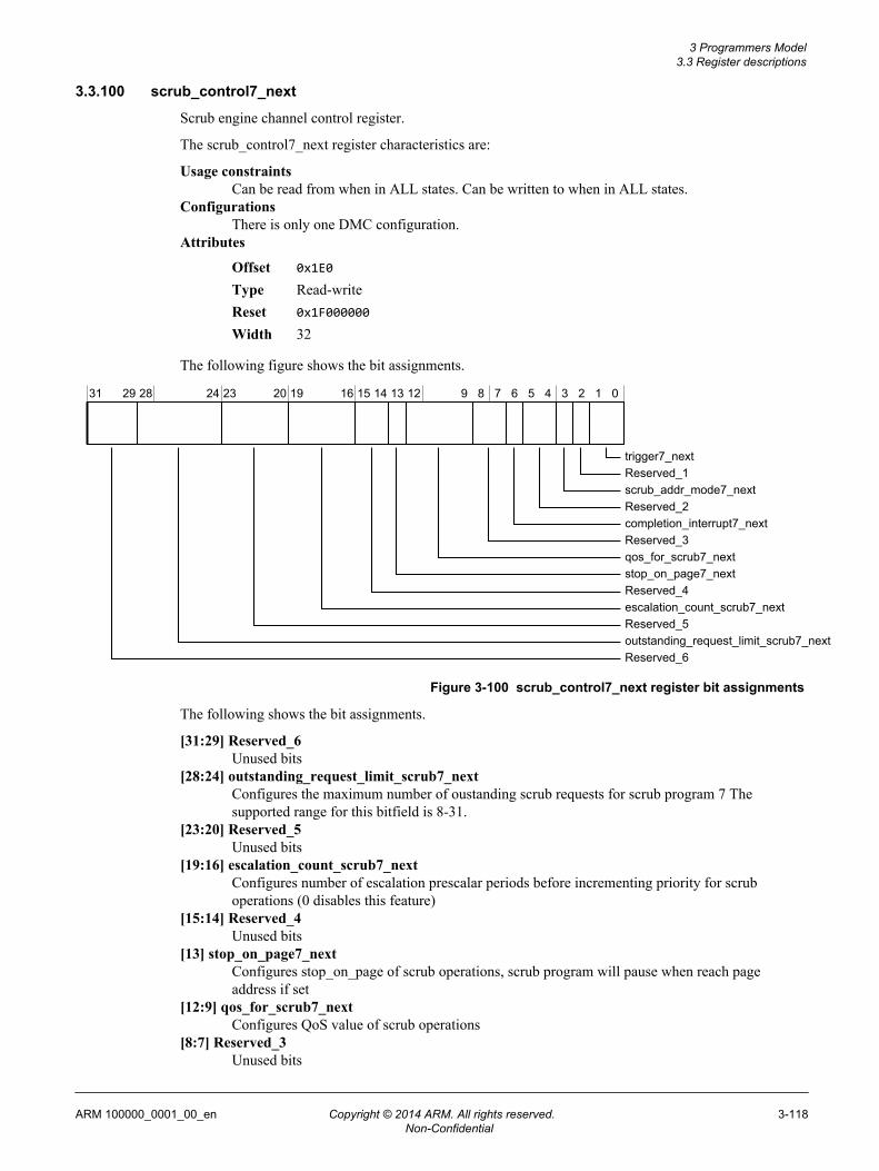
3.3.100 scrub_control7_next
Scrub engine channel control register.
The scrub_control7_next register characteristics are:
Usage constraintsCan be read from when in ALL states. Can be written to when in ALL states.
ConfigurationsThere is only one DMC configuration.
Attributes
Offset 0x1E0
Type Read-writeReset 0x1F000000
Width 32
The following figure shows the bit assignments.
31 29 28 24 23 20 19 16 15 14 13 12 9 8 7 6 5 4 3 2 1 0
scrub_addr_mode7_nextReserved_1trigger7_next
Reserved_2completion_interrupt7_next
stop_on_page7_nextqos_for_scrub7_nextReserved_3
Reserved_5escalation_count_scrub7_nextReserved_4
outstanding_request_limit_scrub7_nextReserved_6
Figure 3-100 scrub_control7_next register bit assignments
The following shows the bit assignments.
[31:29] Reserved_6Unused bits
[28:24] outstanding_request_limit_scrub7_nextConfigures the maximum number of oustanding scrub requests for scrub program 7 Thesupported range for this bitfield is 8-31.
[23:20] Reserved_5Unused bits
[19:16] escalation_count_scrub7_nextConfigures number of escalation prescalar periods before incrementing priority for scruboperations (0 disables this feature)
[15:14] Reserved_4Unused bits
[13] stop_on_page7_nextConfigures stop_on_page of scrub operations, scrub program will pause when reach pageaddress if set
[12:9] qos_for_scrub7_nextConfigures QoS value of scrub operations
[8:7] Reserved_3Unused bits
3 Programmers Model3.3 Register descriptions
ARM 100000_0001_00_en Copyright © 2014 ARM. All rights reserved. 3-118Non-Confidential

[6] completion_interrupt7_nextConfigures whether to emit an event when the sequence completes
[5:4] Reserved_2Unused bits
[3] scrub_addr_mode7_nextConfigures scrub address mode
[2] Reserved_1Unused bits
[1:0] trigger7_nextControls the trigger event associated with the channel operation.
3.3.101 scrub_address_min7_next
Configures the address space control for the scrub engine channel.
The scrub_address_min7_next register characteristics are:
Usage constraintsCan be read from when in ALL states. Can be written to when in ALL states.
ConfigurationsThere is only one DMC configuration.
Attributes
Offset 0x1E4
Type Read-writeReset 0x00000000
Width 32
The following figure shows the bit assignments.
31 0
scrub_address_min7_next
Figure 3-101 scrub_address_min7_next register bit assignments
The following shows the bit assignments.
[31:0] scrub_address_min7_nextProgram to set the starting address for the scrub engine. When scrub_addr_mode7 is set tophysical_address this register specifies logical rank [24:22], physical bank [21:18] and physicalrow address [17:0] directly. When scrub_addr_mode7 is set to system_address this registerspecifies the address in the same address format used by incoming system transactions.
3.3.102 scrub_address_max7_next
Configures the address space control for the scrub engine channel.
The scrub_address_max7_next register characteristics are:
Usage constraintsCan be read from when in ALL states. Can be written to when in ALL states.
ConfigurationsThere is only one DMC configuration.
Attributes
Offset 0x1E8
Type Read-writeReset 0x00000000
Width 32
3 Programmers Model3.3 Register descriptions
ARM 100000_0001_00_en Copyright © 2014 ARM. All rights reserved. 3-119Non-Confidential

The following figure shows the bit assignments.
31 0
scrub_address_max7_next
Figure 3-102 scrub_address_max7_next register bit assignments
The following shows the bit assignments.
[31:0] scrub_address_max7_nextProgram to set the ending address for the scrub engine. When scrub_addr_mode7 is set tophysical_address this register specifies logical rank [24:22], physical bank [21:18] and physicalrow address [17:0] directly. When scrub_addr_mode7 is set to system_address this registerspecifies the address in the same address format used by incoming system transactions.
3.3.103 feature_control_next
Control register for DMC features.
The feature_control_next register characteristics are:
Usage constraintsCan be read from when in ALL states. Can be written to when in ALL states.
ConfigurationsThere is only one DMC configuration.
Attributes
Offset 0x1F0
Type Read-writeReset 0x0AA00000
Width 32
The following figure shows the bit assignments.
31 29 28 27 20 19 18 17 16 15 14 13 12 9 8 7 4 3 2 1 0
Reserved_1crc_enable_nextwrite_dbi_enable_next
two_t_timing_nextzqcs_after_n_ref_next
temp_poll_after_xsref_nexttemp_poll_after_n_ref_nextzqcs_after_xsref_next
address_mirroring_nexttrr_enable_nextReserved_2
mrs_output_inversion_nextlvl_wakeup_en_next
alert_mode_nextaddress_mirroring_mask_nextdfi_err_mode_next
Reserved_3
Figure 3-103 feature_control_next register bit assignments
The following shows the bit assignments.
3 Programmers Model3.3 Register descriptions
ARM 100000_0001_00_en Copyright © 2014 ARM. All rights reserved. 3-120Non-Confidential

[31:29] Reserved_3Unused bits
[28] alert_mode_nextConfigures the DMC behavior in response to dfi_alert_n being asserted.
Note
When performing DIMM CA training using the ALERT pin, this mode must be set to interrupt-only mode.
[27:20] address_mirroring_mask_nextEach bit determines if address mirroring as per the DDR3/DDR4 RDIMM Design Specificationmust be applied to the corresponding rank. Set to 1 to enable mirroring, 0 to disable. Normally,this bit must be set high for odd physical ranks.
[19] dfi_err_mode_nextConfigures the DMC behavior in response to dfi_err being asserted.
[18] lvl_wakeup_en_nextProgram to enable the DMC to bring a rank out of self-refresh to perform PHY training. Thismust not be enabled when using geardown mode.
[17] mrs_output_inversion_nextProgram to enable output inversion for MRS commands for DDR4 DIMMs.
[16] address_mirroring_nextProgram to enable address mirroring for ranks identified by address_mirroring_mask.
[15] trr_enable_nextProgram to enable issue of Target Row Refresh command on detection of potential maximumactivate count (tMAC) violation. Must only be enabled for memories supporting this command.
[14] Reserved_2Unused bits
[13] temp_poll_after_xsref_nextProgram to insert an automatic temperature status poll command following exit from self-refresh.
[12:9] temp_poll_after_n_ref_nextProgram to insert an automatic temperature status poll command following issue of nAUTOREFRESH commands. 0 disables the functionality. 1 is RESERVED
[8] zqcs_after_xsref_nextProgram to insert an automatic ZQC short calibration command following exit from self-refresh.
[7:4] zqcs_after_n_ref_nextProgram to insert an automatic ZQC short calibration command following n refreshes. 0 -disables the functionality. 1 is RESERVED
[3] two_t_timing_nextProgram to enable or disable 2T command timing.
[2] Reserved_1Unused bits
[1] crc_enable_nextProgram to enable or disable Cyclic Redundancy Check (CRC) functionality on write data.
Note
When you enable CRC t_wr, t_wtr and t_wtw must be extended by one cycle to accommodatethe CRC functionality.
[0] write_dbi_enable_nextProgram to enable or disable Data Bus Inversion (DBI) functionality for writes.
3.3.104 mux_control_next
Control muxing options for the DMC.
The mux_control_next register characteristics are:
3 Programmers Model3.3 Register descriptions
ARM 100000_0001_00_en Copyright © 2014 ARM. All rights reserved. 3-121Non-Confidential

Usage constraintsCan be read from when in ALL states. Can be written to when in ALL states.
ConfigurationsThere is only one DMC configuration.
Attributes
Offset 0x1F4
Type Read-writeReset 0x00000000
Width 32
The following figure shows the bit assignments.
31 11 10 8 7 6 5 4 3 2 1 0
Reserved_1
ck_mux_control_nextcke_mux_control_nextcs_mux_control_next
rst_mux_control_nextcid_mask_next
Figure 3-104 mux_control_next register bit assignments
The following shows the bit assignments.
[31:11] Reserved_1Unused bits
[10:8] cid_mask_nextProgram to mask inclusion of dfi_cid[2:0] output in parity calculation, where for each bit ofcid_mask[2:0] a value of 1 means include the corresponding bit of dfi_cid[2:0].
[7:6] rst_mux_control_nextProgram to control muxing of dfi_reset_n output for DIMM applications.
[5:4] ck_mux_control_nextProgram to control muxing of dfi_ck output for DIMM applications.
[3:2] cke_mux_control_nextProgram to control muxing of dfi_cke output for DIMM applications.
[1:0] cs_mux_control_nextProgram to control muxing of dfi_cs_n output for DIMM applications.
3.3.105 rank_remap_control_next
Control register for rank remap.
The rank_remap_control_next register characteristics are:
Usage constraintsCan be read from when in ALL states. Can be written to when in ALL states.
ConfigurationsThere is only one DMC configuration.
Attributes
Offset 0x1F8
Type Read-writeReset 0x76543210
Width 32
The following figure shows the bit assignments.
3 Programmers Model3.3 Register descriptions
ARM 100000_0001_00_en Copyright © 2014 ARM. All rights reserved. 3-122Non-Confidential

31 30 28 27 26 24 23 22 20 19 18 16 15 14 12 11 10 8 7 6 4 3 2 0
rank_remap_cs1_nextrank_mask_cs0_nextrank_remap_cs0_next
rank_mask_cs1_nextrank_remap_cs2_next
rank_mask_cs3_nextrank_remap_cs3_nextrank_mask_cs2_next
rank_remap_cs5_nextrank_mask_cs4_nextrank_remap_cs4_next
rank_mask_cs5_nextrank_remap_cs6_next
rank_mask_cs7_nextrank_remap_cs7_nextrank_mask_cs6_next
Figure 3-105 rank_remap_control_next register bit assignments
The following shows the bit assignments.
[31] rank_mask_cs7_nextProgram to cause the DMC to abort all transactions to DRAM rank 7. Can be used to blocktransactions to a rank that is in maximum power down.
[30:28] rank_remap_cs7_nextProgram to remap rank address 7 to DRAM rank 0..7. Used to remap ranks when replacingDIMMs.
[27] rank_mask_cs6_nextProgram to cause the DMC to abort all transactions to DRAM rank 6. Can be used to blocktransactions to a rank that is in maximum power down.
[26:24] rank_remap_cs6_nextProgram to remap rank address 6 to DRAM rank 0..7. Used to remap ranks when replacingDIMMs.
[23] rank_mask_cs5_nextProgram to cause the DMC to abort all transactions to DRAM rank 5. Can be used to blocktransactions to a rank that is in maximum power down.
[22:20] rank_remap_cs5_nextProgram to remap rank address 5 to DRAM rank 0..7. Used to remap ranks when replacingDIMMs.
[19] rank_mask_cs4_nextProgram to cause the DMC to abort all transactions to DRAM rank 4. Can be used to blocktransactions to a rank that is in maximum power down.
[18:16] rank_remap_cs4_nextProgram to remap rank address 4 to DRAM rank 0..7. Used to remap ranks when replacingDIMMs.
[15] rank_mask_cs3_nextProgram to cause the DMC to abort all transactions to DRAM rank 3. Can be used to blocktransactions to a rank that is in maximum power down.
[14:12] rank_remap_cs3_nextProgram to remap rank address 3 to DRAM rank 0..7. Used to remap ranks when replacingDIMMs.
[11] rank_mask_cs2_nextProgram to cause the DMC to abort all transactions to DRAM rank 2. Can be used to blocktransactions to a rank that is in maximum power down.
3 Programmers Model3.3 Register descriptions
ARM 100000_0001_00_en Copyright © 2014 ARM. All rights reserved. 3-123Non-Confidential

[10:8] rank_remap_cs2_nextProgram to remap rank address 2 to DRAM rank 0..7. Used to remap ranks when replacingDIMMs.
[7] rank_mask_cs1_nextProgram to cause the DMC to abort all transactions to DRAM rank 1. Can be used to blocktransactions to a rank that is in maximum power down.
[6:4] rank_remap_cs1_nextProgram to remap rank address 1 to DRAM rank 0..7. Used to remap ranks when replacingDIMMs.
[3] rank_mask_cs0_nextProgram to cause the DMC to abort all transactions to DRAM rank 0. Can be used to blocktransactions to a rank that is in maximum power down.
[2:0] rank_remap_cs0_nextProgram to remap rank address 0 to DRAM rank 0..7. Used to remap ranks when replacingDIMMs.
3.3.106 scrub_control_next
Scrub engine channel control register.
The scrub_control_next register characteristics are:
Usage constraintsCan be read from when in ALL states. Can be written to when in ALL states.
ConfigurationsThere is only one DMC configuration.
Attributes
Offset 0x1FC
Type Read-writeReset 0x00001F00
Width 32
The following figure shows the bit assignments.
31 15 14 8 7 3 2 0
Reserved_1Reserved_2
outstanding_scrub_request_limit_nextescalation_prescalar_scrub_next
Figure 3-106 scrub_control_next register bit assignments
The following shows the bit assignments.
[31:15] Reserved_2Unused bits
[14:8] outstanding_scrub_request_limit_nextConfigures the maximum number of oustanding scrub requests across all scrub programs Thesupported range for this bitfield is 1-127.
[7:3] Reserved_1Unused bits
[2:0] escalation_prescalar_scrub_nextConfigures escalation prescalar period for use across all scrub programs
3 Programmers Model3.3 Register descriptions
ARM 100000_0001_00_en Copyright © 2014 ARM. All rights reserved. 3-124Non-Confidential

3.3.107 t_refi_next
Configures the refresh interval timing parameter. It must be programmed to the device average all-bankAUTOREFRESH interval, divided by 8.
The t_refi_next register characteristics are:
Usage constraintsCan be read from when in ALL states. Can be written to when in ALL states.
ConfigurationsThere is only one DMC configuration.
Attributes
Offset 0x200
Type Read-writeReset 0x00090100
Width 32
The following figure shows the bit assignments.
31 21 20 16 15 11 10 0
t_refi_nextReserved_1Reserved_2Reserved_3
Figure 3-107 t_refi_next register bit assignments
The following shows the bit assignments.
[31:21] Reserved_3Unused bits
[20:16] Reserved_2Unused bits
[15:11] Reserved_1Unused bits
[10:0] t_refi_nextt_refi_next bitfield. The supported range for this bitfield is 63-2047.
3.3.108 t_rfc_next
Configures the tRFC timing parameter. This determines the delay applied after an AUTOREFRESHcommand before any other command is issued to the same rank.
The t_rfc_next register characteristics are:
Usage constraintsCan be read from when in ALL states. Can be written to when in ALL states.
ConfigurationsThere is only one DMC configuration.
Attributes
Offset 0x204
Type Read-writeReset 0x00008C23
Width 32
The following figure shows the bit assignments.
3 Programmers Model3.3 Register descriptions
ARM 100000_0001_00_en Copyright © 2014 ARM. All rights reserved. 3-125Non-Confidential

31 28 27 20 19 10 9 0
t_rfc_nextt_rfcfg_nextt_rfc_cs_next
Reserved_1
Figure 3-108 t_rfc_next register bit assignments
The following shows the bit assignments.
[31:28] Reserved_1Unused bits
[27:20] t_rfc_cs_nextConfigures the minimum delay between AUTOREFRESH operations to different ranks. Thesupported range for this bitfield is 0-255.
[19:10] t_rfcfg_nextConfigures the tRFC timing parameter for fine-grained AUTOREFRESH operations. Thesupported range for this bitfield is 2-700.
[9:0] t_rfc_nextConfigures the tRFC timing parameter for all-bank AUTOREFRESH operations. The supportedrange for this bitfield is 2-700.
3.3.109 t_mrr_next
Configures the tMRR timing parameter. This determines the Mode Register Read (including Multi-Purpose Register Reads) command delay before any other command is issued to the same rank. Use thisvalue to determine the data cycles returned as a result of an MRR command.
The t_mrr_next register characteristics are:
Usage constraintsCan be read from when in ALL states. Can be written to when in ALL states.
ConfigurationsThere is only one DMC configuration.
Attributes
Offset 0x208
Type Read-writeReset 0x00000002
Width 32
The following figure shows the bit assignments.
31 9 8 7 6 0
t_mrr_nextReserved_2
Reserved_1
Figure 3-109 t_mrr_next register bit assignments
The following shows the bit assignments.
[31:9] Reserved_2Unused bits
[8:7] Reserved_1Unused bits
[6:0] t_mrr_nextt_mrr_next bitfield. The supported range for this bitfield is 1-127.
3 Programmers Model3.3 Register descriptions
ARM 100000_0001_00_en Copyright © 2014 ARM. All rights reserved. 3-126Non-Confidential

3.3.110 t_mrw_next
Configures the tMRW timing parameter. This determines the delay applied after a Mode Register Write(including Multi-Purpose Register Writes) command before any other command is issued to the samerank. Use this value for all delays associated with mode register write and set commands, so the largestof these delays must be programmed.
The t_mrw_next register characteristics are:
Usage constraintsCan be read from when in ALL states. Can be written to when in ALL states.
ConfigurationsThere is only one DMC configuration.
Attributes
Offset 0x20C
Type Read-writeReset 0x0000000C
Width 32
The following figure shows the bit assignments.
31 7 6 0
t_mrw_nextReserved_1
Figure 3-110 t_mrw_next register bit assignments
The following shows the bit assignments.
[31:7] Reserved_1Unused bits
[6:0] t_mrw_nextt_mrw_next bitfield. The supported range for this bitfield is 12-127.
3.3.111 t_rdpden_next
Configures the tRDPDEN timing parameter. This determines the delay applied after a Read commandbefore a power down command can be issued to the same rank.
The t_rdpden_next register characteristics are:
Usage constraintsCan be read from when in ALL states. Can be written to when in ALL states.
ConfigurationsThere is only one DMC configuration.
Attributes
Offset 0x210
Type Read-writeReset 0x0000000A
Width 32
The following figure shows the bit assignments.
31 7 6 0
t_rdpden_nextReserved_1
Figure 3-111 t_rdpden_next register bit assignments
The following shows the bit assignments.
3 Programmers Model3.3 Register descriptions
ARM 100000_0001_00_en Copyright © 2014 ARM. All rights reserved. 3-127Non-Confidential

[31:7] Reserved_1Unused bits
[6:0] t_rdpden_nextt_rdpden_next bitfield. The supported range for this bitfield is 10-126.
3.3.112 t_rcd_next
Configures the tRCD timing parameter. This determines the delay applied after an ACTIVATEcommand before a READ or WRITE command is issued to the same bank.
The t_rcd_next register characteristics are:
Usage constraintsCan be read from when in ALL states. Can be written to when in ALL states.
ConfigurationsThere is only one DMC configuration.
Attributes
Offset 0x218
Type Read-writeReset 0x00000005
Width 32
The following figure shows the bit assignments.
31 5 4 0
t_rcd_nextReserved_1
Figure 3-112 t_rcd_next register bit assignments
The following shows the bit assignments.
[31:5] Reserved_1Unused bits
[4:0] t_rcd_nextt_rcd_next bitfield. The supported range for this bitfield is 4-18.
3.3.113 t_ras_next
Configures the tRAS timing parameter. This determines the delay applied after an ACTIVATE commandbefore a PRECHARGE command is issued to the same bank.
The t_ras_next register characteristics are:
Usage constraintsCan be read from when in ALL states. Can be written to when in ALL states.
ConfigurationsThere is only one DMC configuration.
Attributes
Offset 0x21C
Type Read-writeReset 0x0000000E
Width 32
The following figure shows the bit assignments.
3 Programmers Model3.3 Register descriptions
ARM 100000_0001_00_en Copyright © 2014 ARM. All rights reserved. 3-128Non-Confidential

31 6 5 0
t_ras_nextReserved_1
Figure 3-113 t_ras_next register bit assignments
The following shows the bit assignments.
[31:6] Reserved_1Unused bits
[5:0] t_ras_nextt_ras_next bitfield. The supported range for this bitfield is 8-39.
3.3.114 t_rp_next
Configures the tRP timing parameter. This determines the delay applied after a PRECHARGE commandbefore any other command is issued to the same bank.
The t_rp_next register characteristics are:
Usage constraintsCan be read from when in ALL states. Can be written to when in ALL states.
ConfigurationsThere is only one DMC configuration.
Attributes
Offset 0x220
Type Read-writeReset 0x00000005
Width 32
The following figure shows the bit assignments.
31 5 4 0
t_rp_nextReserved_1
Figure 3-114 t_rp_next register bit assignments
The following shows the bit assignments.
[31:5] Reserved_1Unused bits
[4:0] t_rp_nextt_rp_next bitfield. The supported range for this bitfield is 4-18.
3.3.115 t_rpall_next
Configures the tRPALL timing parameter. This determines the delay applied after a PRECHARGEALLcommand before any other command is issued to the same rank.
The t_rpall_next register characteristics are:
Usage constraintsCan be read from when in ALL states. Can be written to when in ALL states.
ConfigurationsThere is only one DMC configuration.
Attributes
Offset 0x224
Type Read-write
3 Programmers Model3.3 Register descriptions
ARM 100000_0001_00_en Copyright © 2014 ARM. All rights reserved. 3-129Non-Confidential

Reset 0x00000005
Width 32
The following figure shows the bit assignments.
31 5 4 0
t_rpall_nextReserved_1
Figure 3-115 t_rpall_next register bit assignments
The following shows the bit assignments.
[31:5] Reserved_1Unused bits
[4:0] t_rpall_nextt_rpall_next bitfield. The supported range for this bitfield is 4-18.
3.3.116 t_rrd_next
Configures the tRRD timing parameter. This determines the delay applied after an ACTIVATEcommand before another ACTIVATE command is issued to the same rank. The _l and _s fields apply tothe same bank group, and a different bank group, respectively, as described in the DDR4 specification.
The t_rrd_next register characteristics are:
Usage constraintsCan be read from when in ALL states. Can be written to when in ALL states.
ConfigurationsThere is only one DMC configuration.
Attributes
Offset 0x228
Type Read-writeReset 0x00000404
Width 32
The following figure shows the bit assignments.
31 20 19 16 15 12 11 8 7 4 3 0
Reserved_3
t_rrd_l_nextReserved_1t_rrd_s_next
Reserved_2t_rrd_cs_next
Figure 3-116 t_rrd_next register bit assignments
The following shows the bit assignments.
[31:20] Reserved_3Unused bits
[19:16] t_rrd_cs_nextt_rrd_cs_next bitfield. The supported range for this bitfield is 0-15.
[15:12] Reserved_2Unused bits
[11:8] t_rrd_l_nextt_rrd_l_next bitfield. The supported range for this bitfield is 1-15.
3 Programmers Model3.3 Register descriptions
ARM 100000_0001_00_en Copyright © 2014 ARM. All rights reserved. 3-130Non-Confidential
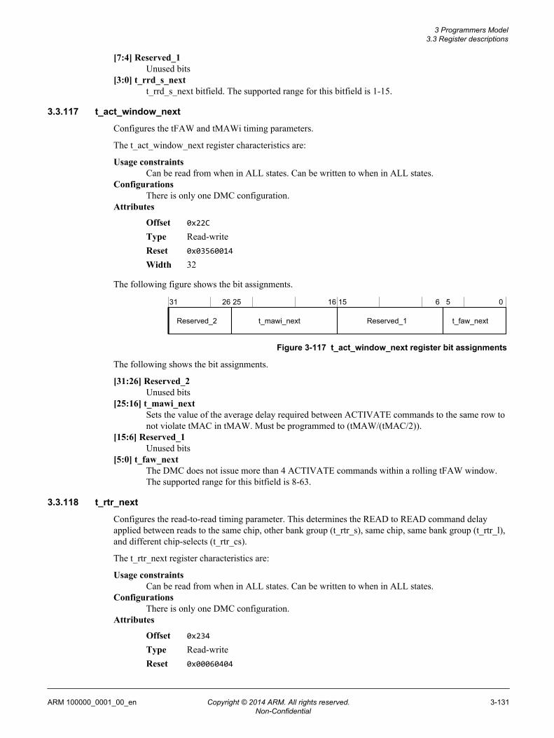
[7:4] Reserved_1Unused bits
[3:0] t_rrd_s_nextt_rrd_s_next bitfield. The supported range for this bitfield is 1-15.
3.3.117 t_act_window_next
Configures the tFAW and tMAWi timing parameters.
The t_act_window_next register characteristics are:
Usage constraintsCan be read from when in ALL states. Can be written to when in ALL states.
ConfigurationsThere is only one DMC configuration.
Attributes
Offset 0x22C
Type Read-writeReset 0x03560014
Width 32
The following figure shows the bit assignments.
31 26 25 16 15 6 5 0
t_faw_nextReserved_1t_mawi_nextReserved_2
Figure 3-117 t_act_window_next register bit assignments
The following shows the bit assignments.
[31:26] Reserved_2Unused bits
[25:16] t_mawi_nextSets the value of the average delay required between ACTIVATE commands to the same row tonot violate tMAC in tMAW. Must be programmed to (tMAW/(tMAC/2)).
[15:6] Reserved_1Unused bits
[5:0] t_faw_nextThe DMC does not issue more than 4 ACTIVATE commands within a rolling tFAW window.The supported range for this bitfield is 8-63.
3.3.118 t_rtr_next
Configures the read-to-read timing parameter. This determines the READ to READ command delayapplied between reads to the same chip, other bank group (t_rtr_s), same chip, same bank group (t_rtr_l),and different chip-selects (t_rtr_cs).
The t_rtr_next register characteristics are:
Usage constraintsCan be read from when in ALL states. Can be written to when in ALL states.
ConfigurationsThere is only one DMC configuration.
Attributes
Offset 0x234
Type Read-writeReset 0x00060404
3 Programmers Model3.3 Register descriptions
ARM 100000_0001_00_en Copyright © 2014 ARM. All rights reserved. 3-131Non-Confidential

Width 32
The following figure shows the bit assignments.
31 25 24 23 21 20 16 15 13 12 8 7 5 4 0
t_rtr_s_nextt_rtr_l_nextReserved_4
t_rtr_cs_nextReserved_2Reserved_1
Reserved_3t_rtr_skip_next
Figure 3-118 t_rtr_next register bit assignments
The following shows the bit assignments.
[31:25] Reserved_4Unused bits
[24] t_rtr_skip_nextEnable when using 2tck preamble to prevent transactions being spaced by t_rtr + 1.
[23:21] Reserved_3Unused bits
[20:16] t_rtr_cs_nextt_rtr_cs_next bitfield. The supported range for this bitfield is 6-31.
[15:13] Reserved_2Unused bits
[12:8] t_rtr_l_nextt_rtr_l_next bitfield. The supported range for this bitfield is 4-31.
[7:5] Reserved_1Unused bits
[4:0] t_rtr_s_nextt_rtr_s_next bitfield. The supported range for this bitfield is 4-31.
3.3.119 t_rtw_next
Configures the read-to-write timing parameter. This determines the READ to WRITE command delayapplied between issued commands to the same chip, other bank group (t_rtw_s), same chip, same bankgroup (t_trw_l), and other chip-selects (t_rtw_cs).
The t_rtw_next register characteristics are:
Usage constraintsCan be read from when in ALL states. Can be written to when in ALL states.
ConfigurationsThere is only one DMC configuration.
Attributes
Offset 0x238
Type Read-writeReset 0x00060606
Width 32
The following figure shows the bit assignments.
3 Programmers Model3.3 Register descriptions
ARM 100000_0001_00_en Copyright © 2014 ARM. All rights reserved. 3-132Non-Confidential

31 21 20 16 15 13 12 8 7 5 4 0
t_rtw_l_nextReserved_3
Reserved_2Reserved_1t_rtw_s_next
t_rtw_cs_next
Figure 3-119 t_rtw_next register bit assignments
The following shows the bit assignments.
[31:21] Reserved_3Unused bits
[20:16] t_rtw_cs_nextt_rtw_cs_next bitfield. The supported range for this bitfield is 4-31.
[15:13] Reserved_2Unused bits
[12:8] t_rtw_l_nextt_rtw_l_next bitfield. The supported range for this bitfield is 4-31.
[7:5] Reserved_1Unused bits
[4:0] t_rtw_s_nextt_rtw_s_next bitfield. The supported range for this bitfield is 4-31.
3.3.120 t_rtp_next
Configures the read-to-precharge timing parameter. This determines the READ to PRECHARGEcommand delay applied between issued commands to the same bank.
The t_rtp_next register characteristics are:
Usage constraintsCan be read from when in ALL states. Can be written to when in ALL states.
ConfigurationsThere is only one DMC configuration.
Attributes
Offset 0x23C
Type Read-writeReset 0x00000004
Width 32
The following figure shows the bit assignments.
31 4 3 0
Reserved_1
t_rtp_next
Figure 3-120 t_rtp_next register bit assignments
The following shows the bit assignments.
[31:4] Reserved_1Unused bits
[3:0] t_rtp_nextt_rtp_next bitfield. The supported range for this bitfield is 4-15.
3 Programmers Model3.3 Register descriptions
ARM 100000_0001_00_en Copyright © 2014 ARM. All rights reserved. 3-133Non-Confidential

3.3.121 t_wr_next
Configures the tWR timing parameter. This determines the write recovery time and is used as the delayapplied between the issue of a WRITE command and subsequent commands, other than WRITEs, to thesame bank. This must take into account CRC timing requirements.
The t_wr_next register characteristics are:
Usage constraintsCan be read from when in ALL states. Can be written to when in ALL states.
ConfigurationsThere is only one DMC configuration.
Attributes
Offset 0x244
Type Read-writeReset 0x00000005
Width 32
The following figure shows the bit assignments.
31 6 5 0
t_wr_nextReserved_1
Figure 3-121 t_wr_next register bit assignments
The following shows the bit assignments.
[31:6] Reserved_1Unused bits
[5:0] t_wr_nextt_wr_next bitfield. The supported range for this bitfield is 5-63.
3.3.122 t_wtr_next
Configures the write-to-read timing parameter, for both same chip, other bank group (tWTR_s), samechip, same bank group (t_WTR_l), and alternate chip (tWTR_cs). These must take into account the CRCtiming requirements.
The t_wtr_next register characteristics are:
Usage constraintsCan be read from when in ALL states. Can be written to when in ALL states.
ConfigurationsThere is only one DMC configuration.
Attributes
Offset 0x248
Type Read-writeReset 0x00040505
Width 32
The following figure shows the bit assignments.
3 Programmers Model3.3 Register descriptions
ARM 100000_0001_00_en Copyright © 2014 ARM. All rights reserved. 3-134Non-Confidential

31 22 21 16 15 14 13 8 7 6 5 0
t_wtr_s_nextt_wtr_l_nextt_wtr_cs_nextReserved_3
Reserved_2Reserved_1
Figure 3-122 t_wtr_next register bit assignments
The following shows the bit assignments.
[31:22] Reserved_3Unused bits
[21:16] t_wtr_cs_nextt_wtr_cs_next bitfield. The supported range for this bitfield is 2-63.
[15:14] Reserved_2Unused bits
[13:8] t_wtr_l_nextt_wtr_l_next bitfield. The supported range for this bitfield is 5-63.
[7:6] Reserved_1Unused bits
[5:0] t_wtr_s_nextt_wtr_s_next bitfield. The supported range for this bitfield is 5-63.
3.3.123 t_wtw_next
Configures the write-to-write timing parameter for same chip, other bank group (t_wtw_s), same chip,same bank group (t_wtw_l), alternate chip (t_wtw_cs) writes. These must take into account CRC timingrequirements.
The t_wtw_next register characteristics are:
Usage constraintsCan be read from when in ALL states. Can be written to when in ALL states.
ConfigurationsThere is only one DMC configuration.
Attributes
Offset 0x24C
Type Read-writeReset 0x00060404
Width 32
The following figure shows the bit assignments.
31 25 24 23 22 21 16 15 14 13 8 7 6 5 0
t_wtw_s_nextt_wtw_l_nextt_wtw_cs_nextReserved_4
Reserved_3Reserved_2Reserved_1
t_wtw_skip_next
Figure 3-123 t_wtw_next register bit assignments
The following shows the bit assignments.
[31:25] Reserved_4Unused bits
[24] t_wtw_skip_nextEnable when using 2tck preamble to prevent transactions being spaced by t_wtw + 1.
3 Programmers Model3.3 Register descriptions
ARM 100000_0001_00_en Copyright © 2014 ARM. All rights reserved. 3-135Non-Confidential

[23:22] Reserved_3Unused bits
[21:16] t_wtw_cs_nextt_wtw_cs_next bitfield. The supported range for this bitfield is 6-35.
[15:14] Reserved_2Unused bits
[13:8] t_wtw_l_nextt_wtw_l_next bitfield. The supported range for this bitfield is 4-35.
[7:6] Reserved_1Unused bits
[5:0] t_wtw_s_nextt_wtw_s_next bitfield. The supported range for this bitfield is 4-35.
3.3.124 t_xmpd_next
Configures the command delay between exiting Maximum Power Down and a subsequent command tothat rank.
The t_xmpd_next register characteristics are:
Usage constraintsCan be read from when in ALL states. Can be written to when in ALL states.
ConfigurationsThere is only one DMC configuration.
Attributes
Offset 0x254
Type Read-writeReset 0x000003FF
Width 32
The following figure shows the bit assignments.
31 12 11 0
t_xmpd_nextReserved_1
Figure 3-124 t_xmpd_next register bit assignments
The following shows the bit assignments.
[31:12] Reserved_1Unused bits
[11:0] t_xmpd_nextt_xmpd_next bitfield. The supported range for this bitfield is 1-4094.
3.3.125 t_ep_next
Configures the enter power-down timing parameter. This parameter is applied between the issue of anactive or precharge power down request and subsequent commands to the same rank.
The t_ep_next register characteristics are:
Usage constraintsCan be read from when in ALL states. Can be written to when in ALL states.
ConfigurationsThere is only one DMC configuration.
Attributes
Offset 0x258
Type Read-write
3 Programmers Model3.3 Register descriptions
ARM 100000_0001_00_en Copyright © 2014 ARM. All rights reserved. 3-136Non-Confidential

Reset 0x00000002
Width 32
The following figure shows the bit assignments.
31 8 7 0
t_ep_nextReserved_1
Figure 3-125 t_ep_next register bit assignments
The following shows the bit assignments.
[31:8] Reserved_1Unused bits
[7:0] t_ep_nextt_ep_next bitfield. The supported range for this bitfield is 1-255.
3.3.126 t_xp_next
Configures the exit power-down timing parameter for operations that do not require a DLL (tXP), andthose that do (tXPDLL). t_xpdll must be greater than or equal to tRCD and tCKE. t_xp must be greaterthan or equal to tMPX_S.
The t_xp_next register characteristics are:
Usage constraintsCan be read from when in ALL states. Can be written to when in ALL states.
ConfigurationsThere is only one DMC configuration.
Attributes
Offset 0x25C
Type Read-writeReset 0x00060002
Width 32
The following figure shows the bit assignments.
31 24 23 16 15 8 7 0
t_xp_nextReserved_1t_xpdll_nextReserved_2
Figure 3-126 t_xp_next register bit assignments
The following shows the bit assignments.
[31:24] Reserved_2Unused bits
[23:16] t_xpdll_nextThis delay is applied for subsequent commands requiring a DLL The supported range for thisbitfield is 5-255.
[15:8] Reserved_1Unused bits
[7:0] t_xp_nextThis delay is applied for subsequent commands not requiring a DLL The supported range forthis bitfield is 1-255.
3 Programmers Model3.3 Register descriptions
ARM 100000_0001_00_en Copyright © 2014 ARM. All rights reserved. 3-137Non-Confidential
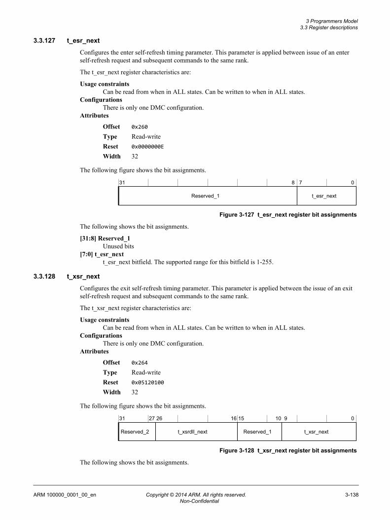
3.3.127 t_esr_next
Configures the enter self-refresh timing parameter. This parameter is applied between issue of an enterself-refresh request and subsequent commands to the same rank.
The t_esr_next register characteristics are:
Usage constraintsCan be read from when in ALL states. Can be written to when in ALL states.
ConfigurationsThere is only one DMC configuration.
Attributes
Offset 0x260
Type Read-writeReset 0x0000000E
Width 32
The following figure shows the bit assignments.
31 8 7 0
t_esr_nextReserved_1
Figure 3-127 t_esr_next register bit assignments
The following shows the bit assignments.
[31:8] Reserved_1Unused bits
[7:0] t_esr_nextt_esr_next bitfield. The supported range for this bitfield is 1-255.
3.3.128 t_xsr_next
Configures the exit self-refresh timing parameter. This parameter is applied between the issue of an exitself-refresh request and subsequent commands to the same rank.
The t_xsr_next register characteristics are:
Usage constraintsCan be read from when in ALL states. Can be written to when in ALL states.
ConfigurationsThere is only one DMC configuration.
Attributes
Offset 0x264
Type Read-writeReset 0x05120100
Width 32
The following figure shows the bit assignments.
31 27 26 16 15 10 9 0
t_xsr_nextReserved_1t_xsrdll_nextReserved_2
Figure 3-128 t_xsr_next register bit assignments
The following shows the bit assignments.
3 Programmers Model3.3 Register descriptions
ARM 100000_0001_00_en Copyright © 2014 ARM. All rights reserved. 3-138Non-Confidential

[31:27] Reserved_2Unused bits
[26:16] t_xsrdll_nextThis delay is applied for subsequent commands requiring a DLL. The supported range for thisbitfield is 1-2047.
[15:10] Reserved_1Unused bits
[9:0] t_xsr_nextThis delay is applied for subsequent commands not requiring a DLL. The supported range forthis bitfield is 1-1023.
3.3.129 t_esrck_next
Configures the delay between entering self-refresh and disabling the DRAM clock. This parameter isapplied when stopping the clock when in self-refresh and when in a maximum power-down state.
The t_esrck_next register characteristics are:
Usage constraintsCan be read from when in ALL states. Can be written to when in ALL states.
ConfigurationsThere is only one DMC configuration.
Attributes
Offset 0x268
Type Read-writeReset 0x00000005
Width 32
The following figure shows the bit assignments.
31 5 4 0
Reserved_1
t_esrck_next
Figure 3-129 t_esrck_next register bit assignments
The following shows the bit assignments.
[31:5] Reserved_1Unused bits
[4:0] t_esrck_nextt_esrck_next bitfield. The supported range for this bitfield is 1-31.
3.3.130 t_ckxsr_next
Configures the delay between DRAM clock enable and exiting self-refresh. This parameter is appliedwhen re-instating the clock when in self-refresh and when in a maximum power-down state.
The t_ckxsr_next register characteristics are:
Usage constraintsCan be read from when in ALL states. Can be written to when in ALL states.
ConfigurationsThere is only one DMC configuration.
Attributes
Offset 0x26C
Type Read-write
3 Programmers Model3.3 Register descriptions
ARM 100000_0001_00_en Copyright © 2014 ARM. All rights reserved. 3-139Non-Confidential

Reset 0x00000001
Width 32
The following figure shows the bit assignments.
31 5 4 0
Reserved_1
t_ckxsr_next
Figure 3-130 t_ckxsr_next register bit assignments
The following shows the bit assignments.
[31:5] Reserved_1Unused bits
[4:0] t_ckxsr_nextt_ckxsr_next bitfield. The supported range for this bitfield is 1-31.
3.3.131 t_cmd_next
Configures command signalling timing.
The t_cmd_next register characteristics are:
Usage constraintsCan be read from when in ALL states. Can be written to when in ALL states.
ConfigurationsThere is only one DMC configuration.
Attributes
Offset 0x270
Type Read-writeReset 0x00000000
Width 32
The following figure shows the bit assignments.
31 12 11 8 7 4 3 0
Reserved_2
t_cal_nextReserved_1t_cmd_lat_next
Figure 3-131 t_cmd_next register bit assignments
The following shows the bit assignments.
[31:12] Reserved_2Unused bits
[11:8] t_cal_nextSpecifies the Command Address latency at the DDR4 device. The supported range for thisbitfield is 0-10.
Note
t_cal must be zero when you use RDIMMs.
[7:4] Reserved_1Unused bits
3 Programmers Model3.3 Register descriptions
ARM 100000_0001_00_en Copyright © 2014 ARM. All rights reserved. 3-140Non-Confidential
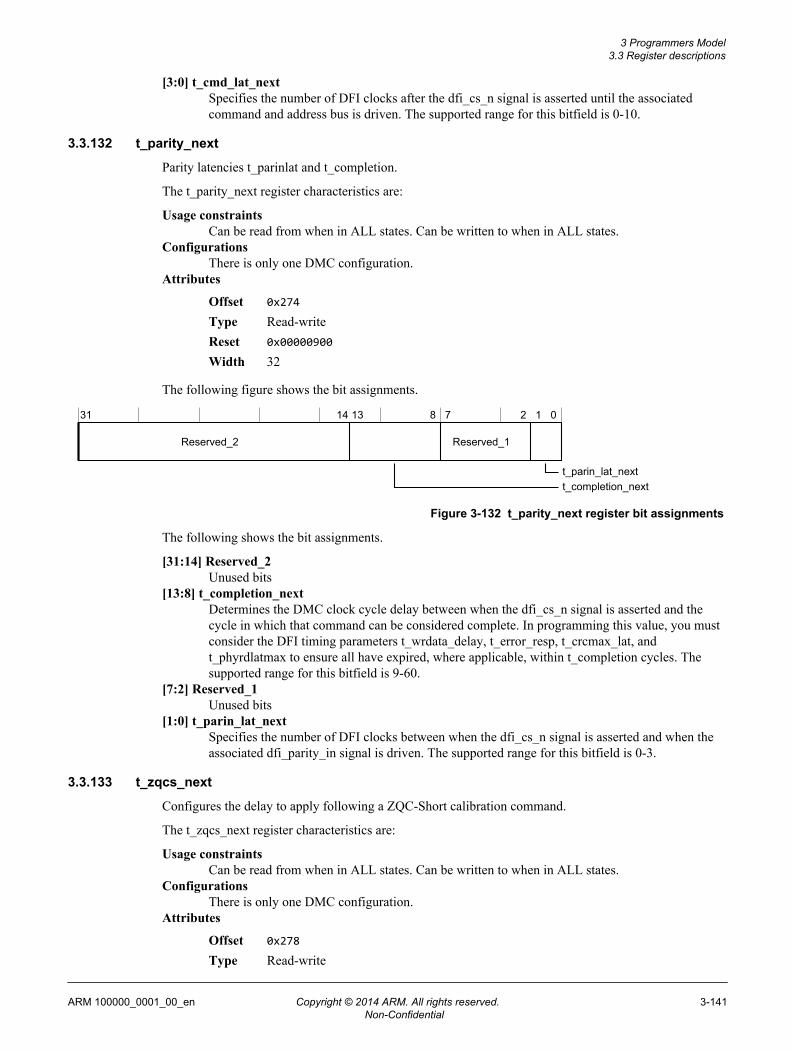
[3:0] t_cmd_lat_nextSpecifies the number of DFI clocks after the dfi_cs_n signal is asserted until the associatedcommand and address bus is driven. The supported range for this bitfield is 0-10.
3.3.132 t_parity_next
Parity latencies t_parinlat and t_completion.
The t_parity_next register characteristics are:
Usage constraintsCan be read from when in ALL states. Can be written to when in ALL states.
ConfigurationsThere is only one DMC configuration.
Attributes
Offset 0x274
Type Read-writeReset 0x00000900
Width 32
The following figure shows the bit assignments.
31 14 13 8 7 2 1 0
Reserved_1Reserved_2
t_completion_nextt_parin_lat_next
Figure 3-132 t_parity_next register bit assignments
The following shows the bit assignments.
[31:14] Reserved_2Unused bits
[13:8] t_completion_nextDetermines the DMC clock cycle delay between when the dfi_cs_n signal is asserted and thecycle in which that command can be considered complete. In programming this value, you mustconsider the DFI timing parameters t_wrdata_delay, t_error_resp, t_crcmax_lat, andt_phyrdlatmax to ensure all have expired, where applicable, within t_completion cycles. Thesupported range for this bitfield is 9-60.
[7:2] Reserved_1Unused bits
[1:0] t_parin_lat_nextSpecifies the number of DFI clocks between when the dfi_cs_n signal is asserted and when theassociated dfi_parity_in signal is driven. The supported range for this bitfield is 0-3.
3.3.133 t_zqcs_next
Configures the delay to apply following a ZQC-Short calibration command.
The t_zqcs_next register characteristics are:
Usage constraintsCan be read from when in ALL states. Can be written to when in ALL states.
ConfigurationsThere is only one DMC configuration.
Attributes
Offset 0x278
Type Read-write
3 Programmers Model3.3 Register descriptions
ARM 100000_0001_00_en Copyright © 2014 ARM. All rights reserved. 3-141Non-Confidential

Reset 0x00000040
Width 32
The following figure shows the bit assignments.
31 10 9 0
t_zqcs_nextReserved_1
Figure 3-133 t_zqcs_next register bit assignments
The following shows the bit assignments.
[31:10] Reserved_1Unused bits
[9:0] t_zqcs_nextt_zqcs_next bitfield. The supported range for this bitfield is 2-1023.
3.3.134 t_rddata_en_next
Determines the time between a READ command commencing on the DFI interface, and the assertion ofthe dfi_read_en signal.
The t_rddata_en_next register characteristics are:
Usage constraintsCan be read from when in ALL states. Can be written to when in ALL states.
ConfigurationsThere is only one DMC configuration.
Attributes
Offset 0x300
Type Read-writeReset 0x00000001
Width 32
The following figure shows the bit assignments.
31 21 20 16 15 14 13 8 7 6 5 0
Reserved_3
t_rddata_en_diff_nextReserved_1t_rddata_en_next
Reserved_2t_phyrdcslat_next
Figure 3-134 t_rddata_en_next register bit assignments
The following shows the bit assignments.
[31:21] Reserved_3Unused bits
[20:16] t_phyrdcslat_nextSpecifies the number of DFI PHY clocks between a READ command commencing on the DFIinterface (assertion of chip-select), and when the associated dfi_rddata_cs_n signal is asserted.The supported range for this bitfield is 0-31.
[15:14] Reserved_2Unused bits
3 Programmers Model3.3 Register descriptions
ARM 100000_0001_00_en Copyright © 2014 ARM. All rights reserved. 3-142Non-Confidential

[13:8] t_rddata_en_diff_nextDescribes a PHY specific value useful for aligning t_rddata_en for a specific PHY. This valuehas no effect on the controller. The supported range for this bitfield is 0-40.
[7:6] Reserved_1Unused bits
[5:0] t_rddata_en_nextt_rddata_en_next bitfield. The supported range for this bitfield is 0-40.
3.3.135 t_phyrdlat_next
Determines the maximum possible time between the assertion of the dfi_read_en signal, and theassertion of the dfi_rddata_valid signal by the PHY.
The t_phyrdlat_next register characteristics are:
Usage constraintsCan be read from when in ALL states. Can be written to when in ALL states.
ConfigurationsThere is only one DMC configuration.
Attributes
Offset 0x304
Type Read-writeReset 0x00000000
Width 32
The following figure shows the bit assignments.
31 6 5 0
Reserved_1
t_phyrdlat_next
Figure 3-135 t_phyrdlat_next register bit assignments
The following shows the bit assignments.
[31:6] Reserved_1Unused bits
[5:0] t_phyrdlat_nextDetermines the maximum time between the assertion of the dfi_read_en signal and the assertionof the dfi_rddata_valid signal by the PHY. The supported range for this bitfield is 2-62.
3.3.136 t_phywrlat_next
Determines the time between a WRITE command commencing on the DFI interface, and the assertion ofthe dfi_wrdata_en, dfi_wrdata_cs and dfi_wrdata signals.
The t_phywrlat_next register characteristics are:
Usage constraintsCan be read from when in ALL states. Can be written to when in ALL states.
ConfigurationsThere is only one DMC configuration.
Attributes
Offset 0x308
Type Read-writeReset 0x00000001
Width 32
3 Programmers Model3.3 Register descriptions
ARM 100000_0001_00_en Copyright © 2014 ARM. All rights reserved. 3-143Non-Confidential

The following figure shows the bit assignments.
31 25 24 23 21 20 16 15 13 12 8 7 5 4 0
Reserved_4
t_phywrlat_diff_nextReserved_1t_phywrlat_next
Reserved_2t_phywrcslat_next
t_phywrdata_nextReserved_3
Figure 3-136 t_phywrlat_next register bit assignments
The following shows the bit assignments.
[31:25] Reserved_4Unused bits
[24] t_phywrdata_nextDetermines the time between the assertion of the dfi_wrdata_en and dfi_wrdata signals. Thesupported range for this bitfield is 0-1.
[23:21] Reserved_3Unused bits
[20:16] t_phywrcslat_nextSpecifies the number of DFI PHY clocks between when a write command is sent on the DFIcontrol interface (dfi_cs_n assertion) and when the associated dfi_wrdata_cs_n signal isasserted. The supported range for this bitfield is 0-31.
[15:13] Reserved_2Unused bits
[12:8] t_phywrlat_diff_nextDescribes the PHY specific value useful for aligning t_phywrlat for a specific PHY. This valuehas no effect on the controller. The supported range for this bitfield is 0-31.
[7:5] Reserved_1Unused bits
[4:0] t_phywrlat_nextDetermines the time between a WRITE command commencing on the DFI interface, and theassertion of the dfi_wrdata_en signal. The supported range for this bitfield is 0-31.
3.3.137 rdlvl_control_next
Determines the DMC behavior during read training operations. See the PHY training interface section ofthe Integration Manual for more details on PHY training.
The rdlvl_control_next register characteristics are:
Usage constraintsCan be read from when in ALL states. Can be written to when in ALL states.
ConfigurationsThere is only one DMC configuration.
Attributes
Offset 0x310
Type Read-writeReset 0x00001080
Width 32
The following figure shows the bit assignments.
3 Programmers Model3.3 Register descriptions
ARM 100000_0001_00_en Copyright © 2014 ARM. All rights reserved. 3-144Non-Confidential

31 25 24 23 20 19 16 15 14 13 12 11 10 9 8 7 5 4 3 1 0
Reserved_7
rdlvl_setup_nextReserved_1rdlvl_mode_next
Reserved_2Reserved_3
rdlvl_refresh_nextReserved_4rdlvl_command_ba1_0_next
Reserved_5rdlvl_err_en_nextrefresh_dur_rdlvl_next
rdlvl_pattern_nextReserved_6rdlvl_preamble_next
Figure 3-137 rdlvl_control_next register bit assignments
The following shows the bit assignments.
[31:25] Reserved_7Unused bits
[24] rdlvl_preamble_nextFor DDR4 program to enable or disable issue of preamble training mode MRS prior toperforming read leveling training.
[23:20] Reserved_6Unused bits
[19:16] rdlvl_pattern_nextProgram the value to be driven onto dfi_lvl_pattern during training. The DMC ignores the value.For default DFI encodings see the DFI specification [5].
[15] Reserved_5Unused bits
[14] rdlvl_err_en_nextIf enabled replay commands because of dfi_err during training.
[13] refresh_dur_rdlvl_nextProgram to enable AUTOREFRESH commands to be generated during training operations.When enabled (1'b1), the DMC exits a training sequence to perform refresh.
[12] rdlvl_refresh_nextProgram to enable or disable issue of an AUTOREFRESH command prior to performing readleveling training.
[11] Reserved_4Unused bits
[10:9] rdlvl_command_ba1_0_nextProgram the BA address to use for training commands.
[8] Reserved_3Unused bits
[7:5] Reserved_2Unused bits
[4] rdlvl_setup_nextProgram the command that sets up the DRAM for read leveling training.
[3:1] Reserved_1Unused bits
[0] rdlvl_mode_nextProgram the mode used for read leveling training.
3 Programmers Model3.3 Register descriptions
ARM 100000_0001_00_en Copyright © 2014 ARM. All rights reserved. 3-145Non-Confidential

3.3.138 rdlvl_mrs_next
Determines the Mode Register command to use to place the DRAM into a training mode for readtraining, when enabled by the rdlvl_control register. See the PHY interface section of the IntegrationManual for more information on PHY training.
The rdlvl_mrs_next register characteristics are:
Usage constraintsCan be read from when in ALL states. Can be written to when in ALL states.
ConfigurationsThere is only one DMC configuration.
Attributes
Offset 0x314
Type Read-writeReset 0x00000004
Width 32
The following figure shows the bit assignments.
31 13 12 0
rdlvl_mrs_nextReserved_1
Figure 3-138 rdlvl_mrs_next register bit assignments
The following shows the bit assignments.
[31:13] Reserved_1Unused bits
[12:0] rdlvl_mrs_nextProgram the Mode Register command the DMC uses to place the DRAM into training mode.Set address bits [2:0] for the Mode Register write to MR3.
3.3.139 t_rdlvl_en_next
Configures the t_rdlvl_en timing parameter. This specifies the cycle delay between assertingdfi_rdlvl_en and the first training command, and also the cycle delay between deasserting dfi_rdlvl_enand performing any subsequent command. It also specifies the minimum delay between trainingcommands and refreshes during training.
The t_rdlvl_en_next register characteristics are:
Usage constraintsCan be read from when in ALL states. Can be written to when in ALL states.
ConfigurationsThere is only one DMC configuration.
Attributes
Offset 0x318
Type Read-writeReset 0x00000000
Width 32
The following figure shows the bit assignments.
3 Programmers Model3.3 Register descriptions
ARM 100000_0001_00_en Copyright © 2014 ARM. All rights reserved. 3-146Non-Confidential

31 6 5 0
Reserved_1
t_rdlvl_en_next
Figure 3-139 t_rdlvl_en_next register bit assignments
The following shows the bit assignments.
[31:6] Reserved_1Unused bits
[5:0] t_rdlvl_en_nextt_rdlvl_en_next bitfield. The supported range for this bitfield is 1-63.
3.3.140 t_rdlvl_rr_next
Configures the t_rdlvl_rr timing parameter. This specifies the cycle delay between training commands. Italso specifies the minimum delay between the last training command and deasserting dfi_rdlvl_en afterobserving dfi_rdlvl_resp.
The t_rdlvl_rr_next register characteristics are:
Usage constraintsCan be read from when in ALL states. Can be written to when in ALL states.
ConfigurationsThere is only one DMC configuration.
Attributes
Offset 0x31C
Type Read-writeReset 0x00000000
Width 32
The following figure shows the bit assignments.
31 10 9 0
t_rdlvl_rr_nextReserved_1
Figure 3-140 t_rdlvl_rr_next register bit assignments
The following shows the bit assignments.
[31:10] Reserved_1Unused bits
[9:0] t_rdlvl_rr_nextt_rdlvl_rr_next bitfield. The supported range for this bitfield is 4-1023.
3.3.141 wrlvl_control_next
Determines the DMC behavior during write training operations. See the PHY training interface sectionof the Integration Manual for more information on PHY training.
The wrlvl_control_next register characteristics are:
Usage constraintsCan be read from when in ALL states. Can be written to when in ALL states.
ConfigurationsThere is only one DMC configuration.
Attributes
Offset 0x320
3 Programmers Model3.3 Register descriptions
ARM 100000_0001_00_en Copyright © 2014 ARM. All rights reserved. 3-147Non-Confidential

Type Read-writeReset 0x00001000
Width 32
The following figure shows the bit assignments.
31 20 19 16 15 14 13 12 11 10 9 8 7 5 4 3 1 0
Reserved_7
wrlvl_setup_nextReserved_1wrlvl_mode_next
Reserved_2Reserved_3
wrlvl_refresh_nextReserved_5Reserved_4
Reserved_6wrlvl_err_en_nextrefresh_dur_wrlvl_next
wrlvl_pattern_next
Figure 3-141 wrlvl_control_next register bit assignments
The following shows the bit assignments.
[31:20] Reserved_7Unused bits
[19:16] wrlvl_pattern_nextProgram the value to be driven onto dfi_lvl_pattern during training. The DMC ignores the value.For default DFI encodings see the DFI specification [5]. The supported range for this bitfield is0-15.
[15] Reserved_6Unused bits
[14] wrlvl_err_en_nextIf enabled replay commands because of dfi_err during training.
[13] refresh_dur_wrlvl_nextProgram to enable AUTOREFRESH commands to be generated during training operations.When enabled (1'b1), the DMC exits a training sequence to perform refresh.
[12] wrlvl_refresh_nextProgram to enable or disable issue of an AUTOREFRESH command prior to performing writeleveling training.
[11] Reserved_5Unused bits
[10:9] Reserved_4Unused bits
[8] Reserved_3Unused bits
[7:5] Reserved_2Unused bits
[4] wrlvl_setup_nextProgram the command that sets up the DRAM for write leveling training.
[3:1] Reserved_1Unused bits
[0] wrlvl_mode_nextProgram the mode used for write leveling training.
3 Programmers Model3.3 Register descriptions
ARM 100000_0001_00_en Copyright © 2014 ARM. All rights reserved. 3-148Non-Confidential

3.3.142 wrlvl_mrs_next
Determines the Mode Register command that the DMC must use to put the DRAM into a training modefor write levelling. You enable this function with the wrlvl_control Register. See the PHY traininginterface section of the Integration Manual for more information.
The wrlvl_mrs_next register characteristics are:
Usage constraintsCan be read from when in ALL states. Can be written to when in ALL states.
ConfigurationsThere is only one DMC configuration.
Attributes
Offset 0x324
Type Read-writeReset 0x00000086
Width 32
The following figure shows the bit assignments.
31 13 12 0
wrlvl_mrs_nextReserved_1
Figure 3-142 wrlvl_mrs_next register bit assignments
The following shows the bit assignments.
[31:13] Reserved_1Unused bits
[12:0] wrlvl_mrs_nextProgram the command the DMC uses to place the DRAM into training mode. Set address bits[12:0] for the Mode Register write to MR1.
3.3.143 t_wrlvl_en_next
Configures the t_wrlvl_en timing parameter. Specifies the cycle delay between asserting ODT fortraining and asserting dfi_wrlvl_en, the delay between asserting dfi_wrlvl_en and the first trainingcommand, the delay between deasserting dfi_wrlvl_en and de-asserting ODT, and deasserting ODT toany subsequent command. It is also used between ODT transitions and refreshes generated duringtraining.
The t_wrlvl_en_next register characteristics are:
Usage constraintsCan be read from when in ALL states. Can be written to when in ALL states.
ConfigurationsThere is only one DMC configuration.
Attributes
Offset 0x328
Type Read-writeReset 0x00000000
Width 32
The following figure shows the bit assignments.
3 Programmers Model3.3 Register descriptions
ARM 100000_0001_00_en Copyright © 2014 ARM. All rights reserved. 3-149Non-Confidential
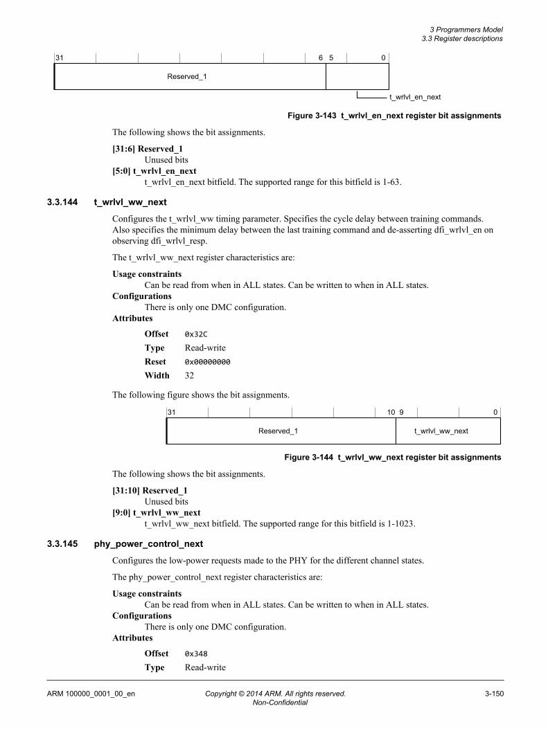
31 6 5 0
Reserved_1
t_wrlvl_en_next
Figure 3-143 t_wrlvl_en_next register bit assignments
The following shows the bit assignments.
[31:6] Reserved_1Unused bits
[5:0] t_wrlvl_en_nextt_wrlvl_en_next bitfield. The supported range for this bitfield is 1-63.
3.3.144 t_wrlvl_ww_next
Configures the t_wrlvl_ww timing parameter. Specifies the cycle delay between training commands.Also specifies the minimum delay between the last training command and de-asserting dfi_wrlvl_en onobserving dfi_wrlvl_resp.
The t_wrlvl_ww_next register characteristics are:
Usage constraintsCan be read from when in ALL states. Can be written to when in ALL states.
ConfigurationsThere is only one DMC configuration.
Attributes
Offset 0x32C
Type Read-writeReset 0x00000000
Width 32
The following figure shows the bit assignments.
31 10 9 0
t_wrlvl_ww_nextReserved_1
Figure 3-144 t_wrlvl_ww_next register bit assignments
The following shows the bit assignments.
[31:10] Reserved_1Unused bits
[9:0] t_wrlvl_ww_nextt_wrlvl_ww_next bitfield. The supported range for this bitfield is 1-1023.
3.3.145 phy_power_control_next
Configures the low-power requests made to the PHY for the different channel states.
The phy_power_control_next register characteristics are:
Usage constraintsCan be read from when in ALL states. Can be written to when in ALL states.
ConfigurationsThere is only one DMC configuration.
Attributes
Offset 0x348
Type Read-write
3 Programmers Model3.3 Register descriptions
ARM 100000_0001_00_en Copyright © 2014 ARM. All rights reserved. 3-150Non-Confidential

Reset 0x00000000
Width 32
The following figure shows the bit assignments.
31 28 27 24 23 20 19 16 15 12 11 8 7 5 4 3 2 1 0
lp_sref_en_nextlp_pd_en_nextlp_idle_en_next
lp_mpd_en_nextlp_arch_en_next
lp_wakeup_pd_nextlp_wakeup_idle_nextReserved_1
lp_wakeup_arch_nextlp_wakeup_mpd_nextlp_wakeup_sref_next
Reserved_2
Figure 3-145 phy_power_control_next register bit assignments
The following shows the bit assignments.
[31:28] Reserved_2Unused bits
[27:24] lp_wakeup_arch_nextProgram the PHY wakeup encoding for PHY low-power requests when entering LOW-POWERarchitectural state. The supported range for this bitfield is 0-15.
[23:20] lp_wakeup_mpd_nextProgram the PHY wakeup encoding for PHY low-power requests when in MPD. The supportedrange for this bitfield is 0-15.
[19:16] lp_wakeup_sref_nextProgram the PHY wakeup encoding for PHY low-power requests when in self-refresh. Thesupported range for this bitfield is 0-15.
[15:12] lp_wakeup_pd_nextProgram the PHY wakeup encoding for PHY low-power requests when powered down. Thesupported range for this bitfield is 0-15.
[11:8] lp_wakeup_idle_nextProgram the PHY wakeup encoding for PHY low-power requests when idle. The supportedrange for this bitfield is 0-15.
[7:5] Reserved_1Unused bits
[4] lp_arch_en_nextProgram to enable or disable a PHY low-power request when entering LOW-POWERarchitectural state.
[3] lp_mpd_en_nextProgram to enable or disable a PHY low-power request when in MPD.
[2] lp_sref_en_nextProgram to enable or disable a PHY low-power request when in self-refresh.
[1] lp_pd_en_nextProgram to enable or disable a PHY low-power request when in power down.
[0] lp_idle_en_nextProgram to enable or disable a PHY low-power request when idle.
3 Programmers Model3.3 Register descriptions
ARM 100000_0001_00_en Copyright © 2014 ARM. All rights reserved. 3-151Non-Confidential

3.3.146 t_lpresp_next
Configures the minimum cycle delay to apply for PHY low-power handshakes.
The t_lpresp_next register characteristics are:
Usage constraintsCan be read from when in ALL states. Can be written to when in ALL states.
ConfigurationsThere is only one DMC configuration.
Attributes
Offset 0x34C
Type Read-writeReset 0x00000000
Width 32
The following figure shows the bit assignments.
31 3 2 0
Reserved_1
t_lpresp_next
Figure 3-146 t_lpresp_next register bit assignments
The following shows the bit assignments.
[31:3] Reserved_1Unused bits
[2:0] t_lpresp_nextThe DMC waits a minimum t_lpresp cycles after asserting a PHY low power request beforedeasserting the request and resuming other commands. Zero means wait for dfi_lp_ack. Thesupported range for this bitfield is 0-7.
3.3.147 phy_update_control_next
Configures the update mechanism to use in response to PHY training requests.
The phy_update_control_next register characteristics are:
Usage constraintsCan be read from when in ALL states. Can be written to when in ALL states.
ConfigurationsThere is only one DMC configuration.
Attributes
Offset 0x350
Type Read-writeReset 0x0FE00000
Width 32
The following figure shows the bit assignments.
3 Programmers Model3.3 Register descriptions
ARM 100000_0001_00_en Copyright © 2014 ARM. All rights reserved. 3-152Non-Confidential

31 29 28 27 21 20 19 16 15 14 13 12 11 10 9 8 7 6 5 4 3 2 1 0
phyupd_type_01_nextReserved_1phyupd_type_00_next
Reserved_2phyupd_type_10_next
Reserved_4phyupd_type_11_nextReserved_3
t_ctrlupd_min_nextctrlupd_after_xsref_nextctrlupd_after_n_ref_next
phyupd_mode_nextReserved_5
Figure 3-147 phy_update_control_next register bit assignments
The following shows the bit assignments.
[31:29] Reserved_5Unused bits
[28] phyupd_mode_nextConfigures the DMC behavior in response to dfi_phyupd_req being asserted.
[27:21] t_ctrlupd_min_nextSets the number of cycles the DMC waits for acknowledgment of a cltrupd_req beforedeasserting the request and continuing normal operation. A value of 0x0 indicates the DMCmust always wait for an acknowledgment before proceeding. The supported range for thisbitfield is 0-127.
[20] ctrlupd_after_xsref_nextProgram to enable an automatic DMC-initiated PHY update request after exiting self-refresh
[19:16] ctrlupd_after_n_ref_nextProgram to enable an automatic DMC-initiated PHY update request after every nAUTOREFRESH commands. Zero disables the functionality. One is RESERVED
[15:14] Reserved_4Unused bits
[13:12] phyupd_type_11_nextProgram the required response to PHY update requests of type 11.
[11:10] Reserved_3Unused bits
[9:8] phyupd_type_10_nextProgram the required response to PHY update requests of type 10.
[7:6] Reserved_2Unused bits
[5:4] phyupd_type_01_nextProgram the required response to PHY update requests of type 01.
[3:2] Reserved_1Unused bits
[1:0] phyupd_type_00_nextProgram the required response to PHY update requests of type 00.
3.3.148 odt_timing_next
Configures the ODT on and off timing.
The odt_timing_next register characteristics are:
3 Programmers Model3.3 Register descriptions
ARM 100000_0001_00_en Copyright © 2014 ARM. All rights reserved. 3-153Non-Confidential

Usage constraintsCan be read from when in ALL states. Can be written to when in ALL states.
ConfigurationsThere is only one DMC configuration.
Attributes
Offset 0x358
Type Read-writeReset 0x06000600
Width 32
The following figure shows the bit assignments.
31 29 28 24 23 21 20 16 15 13 12 8 7 5 4 0
t_odt_off_wr_nextReserved_1t_odt_on_wr_next
Reserved_2t_odt_on_rd_next
Reserved_4t_odt_off_rd_nextReserved_3
Figure 3-148 odt_timing_next register bit assignments
The following shows the bit assignments.
[31:29] Reserved_4Unused bits
[28:24] t_odt_off_rd_nextTime from cs assertion to ODT being deasserted for read. The supported range for this bitfield is2-31.
[23:21] Reserved_3Unused bits
[20:16] t_odt_on_rd_nextTime from cs assertion to ODT being asserted for read. The supported range for this bitfield is0-29.
[15:13] Reserved_2Unused bits
[12:8] t_odt_off_wr_nextTime from cs assertion to ODT being deasserted for write. The supported range for this bitfieldis 2-31.
[7:5] Reserved_1Unused bits
[4:0] t_odt_on_wr_nextTime from cs assertion to ODT being asserted for write. The supported range for this bitfield is0-29.
3.3.149 odt_wr_control_31_00_next
Configures the ODT on and off settings for active and inactive ranks during writes.
The odt_wr_control_31_00_next register characteristics are:
Usage constraintsCan be read from when in ALL states. Can be written to when in ALL states.
3 Programmers Model3.3 Register descriptions
ARM 100000_0001_00_en Copyright © 2014 ARM. All rights reserved. 3-154Non-Confidential
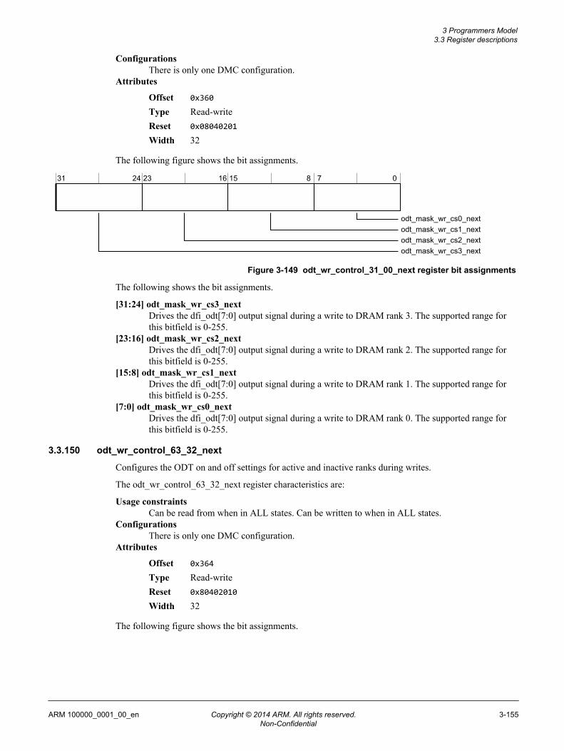
ConfigurationsThere is only one DMC configuration.
Attributes
Offset 0x360
Type Read-writeReset 0x08040201
Width 32
The following figure shows the bit assignments.
31 24 23 16 15 8 7 0
odt_mask_wr_cs2_nextodt_mask_wr_cs1_nextodt_mask_wr_cs0_next
odt_mask_wr_cs3_next
Figure 3-149 odt_wr_control_31_00_next register bit assignments
The following shows the bit assignments.
[31:24] odt_mask_wr_cs3_nextDrives the dfi_odt[7:0] output signal during a write to DRAM rank 3. The supported range forthis bitfield is 0-255.
[23:16] odt_mask_wr_cs2_nextDrives the dfi_odt[7:0] output signal during a write to DRAM rank 2. The supported range forthis bitfield is 0-255.
[15:8] odt_mask_wr_cs1_nextDrives the dfi_odt[7:0] output signal during a write to DRAM rank 1. The supported range forthis bitfield is 0-255.
[7:0] odt_mask_wr_cs0_nextDrives the dfi_odt[7:0] output signal during a write to DRAM rank 0. The supported range forthis bitfield is 0-255.
3.3.150 odt_wr_control_63_32_next
Configures the ODT on and off settings for active and inactive ranks during writes.
The odt_wr_control_63_32_next register characteristics are:
Usage constraintsCan be read from when in ALL states. Can be written to when in ALL states.
ConfigurationsThere is only one DMC configuration.
Attributes
Offset 0x364
Type Read-writeReset 0x80402010
Width 32
The following figure shows the bit assignments.
3 Programmers Model3.3 Register descriptions
ARM 100000_0001_00_en Copyright © 2014 ARM. All rights reserved. 3-155Non-Confidential

31 24 23 16 15 8 7 0
odt_mask_wr_cs6_nextodt_mask_wr_cs5_nextodt_mask_wr_cs4_next
odt_mask_wr_cs7_next
Figure 3-150 odt_wr_control_63_32_next register bit assignments
The following shows the bit assignments.
[31:24] odt_mask_wr_cs7_nextDrives the dfi_odt[7:0] output signal during a write to DRAM rank 7. The supported range forthis bitfield is 0-255.
[23:16] odt_mask_wr_cs6_nextDrives the dfi_odt[7:0] output signal during a write to DRAM rank 6. The supported range forthis bitfield is 0-255.
[15:8] odt_mask_wr_cs5_nextDrives the dfi_odt[7:0] output signal during a write to DRAM rank 5. The supported range forthis bitfield is 0-255.
[7:0] odt_mask_wr_cs4_nextDrives the dfi_odt[7:0] output signal during a write to DRAM rank 4. The supported range forthis bitfield is 0-255.
3.3.151 odt_rd_control_31_00_next
Configures the ODT on and off settings for active and inactive ranks during reads.
The odt_rd_control_31_00_next register characteristics are:
Usage constraintsCan be read from when in ALL states. Can be written to when in ALL states.
ConfigurationsThere is only one DMC configuration.
Attributes
Offset 0x368
Type Read-writeReset 0x00000000
Width 32
The following figure shows the bit assignments.
31 24 23 16 15 8 7 0
odt_mask_rd_cs2_nextodt_mask_rd_cs1_nextodt_mask_rd_cs0_next
odt_mask_rd_cs3_next
Figure 3-151 odt_rd_control_31_00_next register bit assignments
The following shows the bit assignments.
[31:24] odt_mask_rd_cs3_nextDrives the dfi_odt[7:0] output signal during a read to DRAM rank 3. The supported range forthis bitfield is 0-255.
3 Programmers Model3.3 Register descriptions
ARM 100000_0001_00_en Copyright © 2014 ARM. All rights reserved. 3-156Non-Confidential

[23:16] odt_mask_rd_cs2_nextDrives the dfi_odt[7:0] output signal during a read to DRAM rank 2. The supported range forthis bitfield is 0-255.
[15:8] odt_mask_rd_cs1_nextDrives the dfi_odt[7:0] output signal during a read to DRAM rank 1. The supported range forthis bitfield is 0-255.
[7:0] odt_mask_rd_cs0_nextDrives the dfi_odt[7:0] output signal during a read to DRAM rank 0. The supported range forthis bitfield is 0-255.
3.3.152 odt_rd_control_63_32_next
Configures the ODT on and off settings for active and inactive ranks during reads.
The odt_rd_control_63_32_next register characteristics are:
Usage constraintsCan be read from when in ALL states. Can be written to when in ALL states.
ConfigurationsThere is only one DMC configuration.
Attributes
Offset 0x36C
Type Read-writeReset 0x00000000
Width 32
The following figure shows the bit assignments.
31 24 23 16 15 8 7 0
odt_mask_rd_cs6_nextodt_mask_rd_cs5_nextodt_mask_rd_cs4_next
odt_mask_rd_cs7_next
Figure 3-152 odt_rd_control_63_32_next register bit assignments
The following shows the bit assignments.
[31:24] odt_mask_rd_cs7_nextDrives the dfi_odt[7:0] output signal during a read to DRAM rank 7. The supported range forthis bitfield is 0-255.
[23:16] odt_mask_rd_cs6_nextDrives the dfi_odt[7:0] output signal during a read to DRAM rank 6. The supported range forthis bitfield is 0-255.
[15:8] odt_mask_rd_cs5_nextDrives the dfi_odt[7:0] output signal during a read to DRAM rank 5. The supported range forthis bitfield is 0-255.
[7:0] odt_mask_rd_cs4_nextDrives the dfi_odt[7:0] output signal during a read to DRAM rank 4. The supported range forthis bitfield is 0-255.
3.3.153 temperature_readout
Holds the status of the temperature information. Reading the register returns the current temperaturefrom the most recent automated temperature poll.
The temperature_readout register characteristics are:
3 Programmers Model3.3 Register descriptions
ARM 100000_0001_00_en Copyright © 2014 ARM. All rights reserved. 3-157Non-Confidential
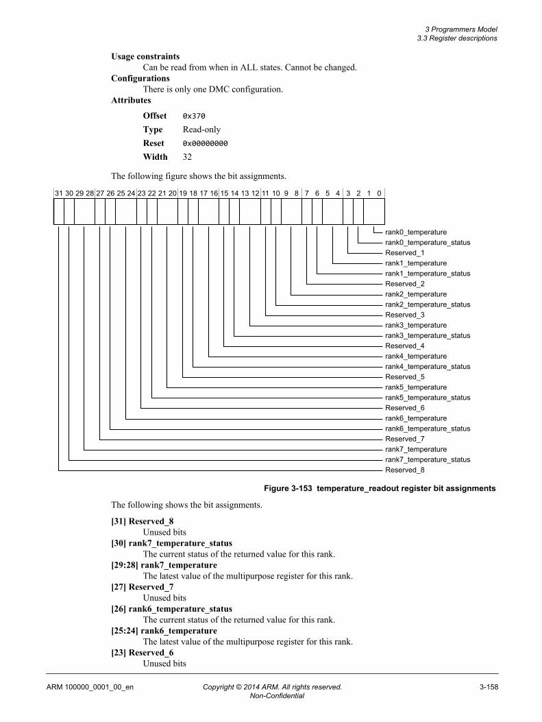
Usage constraintsCan be read from when in ALL states. Cannot be changed.
ConfigurationsThere is only one DMC configuration.
Attributes
Offset 0x370
Type Read-onlyReset 0x00000000
Width 32
The following figure shows the bit assignments.
31 30 29 28 27 26 25 24 23 22 21 20 19 18 17 16 15 14 13 12 11 10 9 8 7 6 5 4 3 2 1 0
Reserved_1rank0_temperature_statusrank0_temperature
rank1_temperaturerank1_temperature_status
rank2_temperature_statusrank2_temperatureReserved_2
rank3_temperature_statusrank3_temperatureReserved_3
Reserved_4rank4_temperature
rank5_temperatureReserved_5rank4_temperature_status
rank6_temperatureReserved_6rank5_temperature_status
rank6_temperature_statusReserved_7
Reserved_8rank7_temperature_statusrank7_temperature
Figure 3-153 temperature_readout register bit assignments
The following shows the bit assignments.
[31] Reserved_8Unused bits
[30] rank7_temperature_statusThe current status of the returned value for this rank.
[29:28] rank7_temperatureThe latest value of the multipurpose register for this rank.
[27] Reserved_7Unused bits
[26] rank6_temperature_statusThe current status of the returned value for this rank.
[25:24] rank6_temperatureThe latest value of the multipurpose register for this rank.
[23] Reserved_6Unused bits
3 Programmers Model3.3 Register descriptions
ARM 100000_0001_00_en Copyright © 2014 ARM. All rights reserved. 3-158Non-Confidential
[22] rank5_temperature_statusThe current status of the returned value for this rank.
[21:20] rank5_temperatureThe latest value of the multipurpose register for this rank.
[19] Reserved_5Unused bits
[18] rank4_temperature_statusThe current status of the returned value for this rank.
[17:16] rank4_temperatureThe latest value of the multipurpose register for this rank.
[15] Reserved_4Unused bits
[14] rank3_temperature_statusThe current status of the returned value for this rank.
[13:12] rank3_temperatureThe latest value of the multipurpose register for this rank.
[11] Reserved_3Unused bits
[10] rank2_temperature_statusThe current status of the returned value for this rank.
[9:8] rank2_temperatureThe latest value of the multipurpose register for this rank.
[7] Reserved_2Unused bits
[6] rank1_temperature_statusThe current status of the returned value for this rank.
[5:4] rank1_temperatureThe latest value of the multipurpose register for this rank.
[3] Reserved_1Unused bits
[2] rank0_temperature_statusThe current status of the returned value for this rank.
[1:0] rank0_temperatureThe latest value of the multipurpose register for this rank.
3.3.154 training_status
Shows information relating to the training request status of the DMC.
The training_status register characteristics are:
Usage constraintsCan be read from when in ALL states. Cannot be changed.
ConfigurationsThere is only one DMC configuration.
Attributes
Offset 0x378
Type Read-onlyReset 0x00000000
Width 32
The following figure shows the bit assignments.
3 Programmers Model3.3 Register descriptions
ARM 100000_0001_00_en Copyright © 2014 ARM. All rights reserved. 3-159Non-Confidential

31 24 23 16 15 8 7 0
wrlvl_training_chiprdlvl_training_chipphy_training_chip
rdlvl_gate_training_chip
Figure 3-154 training_status register bit assignments
The following shows the bit assignments.
[31:24] phy_training_chipOne bit per rank indicating that the PHY has an outstanding request for PHY training on theindicated DRAM rank.
[23:16] rdlvl_training_chipOne bit per rank indicating that the PHY has an outstanding request for rdlvl gate training on theindicated DRAM rank.
[15:8] rdlvl_gate_training_chipWaiting for rdlvl gate training on the indicated DRAM rank.
[7:0] wrlvl_training_chipOne bit per rank indicating that the PHY has an outstanding request for wrlvl training on theindicated DRAM rank.
3.3.155 update_status
Shows information relating to the update request status of the DMC.
The update_status register characteristics are:
Usage constraintsCan be read from when in ALL states. Cannot be changed.
ConfigurationsThere is only one DMC configuration.
Attributes
Offset 0x37C
Type Read-onlyReset 0x00000000
Width 32
The following figure shows the bit assignments.
31 3 2 1 0
Reserved_1
phyupd_typephyupd_req
Figure 3-155 update_status register bit assignments
The following shows the bit assignments.
[31:3] Reserved_1Unused bits
[2:1] phyupd_typeIndicates the type of the PHY update request.
[0] phyupd_reqIndicates that the PHY has an outstanding request for an update.
3 Programmers Model3.3 Register descriptions
ARM 100000_0001_00_en Copyright © 2014 ARM. All rights reserved. 3-160Non-Confidential

3.3.156 dq_map_control_15_00_next
Controls the DQ mapping compensation applied for CRC calculation. For each nibble of the DQ bus, theDIMM SPD defines a DQ Map Index to define the bit connectivity to each rank. Program the DQ MapIndex retrieved from the SPD for each nibble into the corresponding register in the DMC for correctCRC operation.
The dq_map_control_15_00_next register characteristics are:
Usage constraintsCan be read from when in ALL states. Can be written to when in ALL states.
ConfigurationsThere is only one DMC configuration.
Attributes
Offset 0x380
Type Read-writeReset 0x00000000
Width 32
The following figure shows the bit assignments.
31 30 29 24 23 22 21 16 15 14 13 8 7 6 5 0
dq_map_7_4_nextReserved_1dq_map_3_0_next
Reserved_2dq_map_11_8_next
Reserved_4dq_map_15_12_nextReserved_3
Figure 3-156 dq_map_control_15_00_next register bit assignments
The following shows the bit assignments.
[31:30] Reserved_4Unused bits
[29:24] dq_map_15_12_nextControls DQ mapping for bits [15:12] of the DQ bus.
[23:22] Reserved_3Unused bits
[21:16] dq_map_11_8_nextControls DQ mapping for bits [11:8] of the DQ bus.
[15:14] Reserved_2Unused bits
[13:8] dq_map_7_4_nextControls DQ mapping for bits [7:4] of the DQ bus.
[7:6] Reserved_1Unused bits
[5:0] dq_map_3_0_nextControls DQ mapping for bits [3:0] of the DQ bus.
3.3.157 dq_map_control_31_16_next
Controls the DQ mapping compensation applied for CRC calculation. For each nibble of the DQ bus, theDIMM SPD defines a DQ Map Index to define the bit connectivity to each rank. Program the DQ Map
3 Programmers Model3.3 Register descriptions
ARM 100000_0001_00_en Copyright © 2014 ARM. All rights reserved. 3-161Non-Confidential
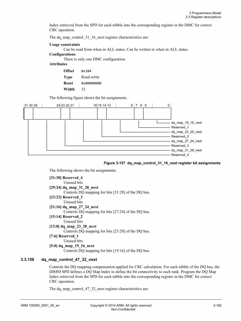
Index retrieved from the SPD for each nibble into the corresponding register in the DMC for correctCRC operation.
The dq_map_control_31_16_next register characteristics are:
Usage constraintsCan be read from when in ALL states. Can be written to when in ALL states.
ConfigurationsThere is only one DMC configuration.
Attributes
Offset 0x384
Type Read-writeReset 0x00000000
Width 32
The following figure shows the bit assignments.
31 30 29 24 23 22 21 16 15 14 13 8 7 6 5 0
dq_map_23_20_nextReserved_1dq_map_19_16_next
Reserved_2dq_map_27_24_next
Reserved_4dq_map_31_28_nextReserved_3
Figure 3-157 dq_map_control_31_16_next register bit assignments
The following shows the bit assignments.
[31:30] Reserved_4Unused bits
[29:24] dq_map_31_28_nextControls DQ mapping for bits [31:28] of the DQ bus.
[23:22] Reserved_3Unused bits
[21:16] dq_map_27_24_nextControls DQ mapping for bits [27:24] of the DQ bus.
[15:14] Reserved_2Unused bits
[13:8] dq_map_23_20_nextControls DQ mapping for bits [23:20] of the DQ bus.
[7:6] Reserved_1Unused bits
[5:0] dq_map_19_16_nextControls DQ mapping for bits [19:16] of the DQ bus.
3.3.158 dq_map_control_47_32_next
Controls the DQ mapping compensation applied for CRC calculation. For each nibble of the DQ bus, theDIMM SPD defines a DQ Map Index to define the bit connectivity to each rank. Program the DQ MapIndex retrieved from the SPD for each nibble into the corresponding register in the DMC for correctCRC operation.
The dq_map_control_47_32_next register characteristics are:
3 Programmers Model3.3 Register descriptions
ARM 100000_0001_00_en Copyright © 2014 ARM. All rights reserved. 3-162Non-Confidential

Usage constraintsCan be read from when in ALL states. Can be written to when in ALL states.
ConfigurationsThere is only one DMC configuration.
Attributes
Offset 0x388
Type Read-writeReset 0x00000000
Width 32
The following figure shows the bit assignments.
31 30 29 24 23 22 21 16 15 14 13 8 7 6 5 0
dq_map_39_36_nextReserved_1dq_map_35_32_next
Reserved_2dq_map_43_40_next
Reserved_4dq_map_47_44_nextReserved_3
Figure 3-158 dq_map_control_47_32_next register bit assignments
The following shows the bit assignments.
[31:30] Reserved_4Unused bits
[29:24] dq_map_47_44_nextControls DQ mapping for bits [47:44] of the DQ bus.
[23:22] Reserved_3Unused bits
[21:16] dq_map_43_40_nextControls DQ mapping for bits [43:40] of the DQ bus.
[15:14] Reserved_2Unused bits
[13:8] dq_map_39_36_nextControls DQ mapping for bits [39:36] of the DQ bus.
[7:6] Reserved_1Unused bits
[5:0] dq_map_35_32_nextControls DQ mapping for bits [35:32] of the DQ bus.
3.3.159 dq_map_control_63_48_next
Controls the DQ mapping compensation applied for CRC calculation. For each nibble of the DQ bus, theDIMM SPD defines a DQ Map Index to define the bit connectivity to each rank. Program the DQ MapIndex retrieved from the SPD for each nibble into the corresponding register in the DMC for correctCRC operation.
The dq_map_control_63_48_next register characteristics are:
Usage constraintsCan be read from when in ALL states. Can be written to when in ALL states.
ConfigurationsThere is only one DMC configuration.
3 Programmers Model3.3 Register descriptions
ARM 100000_0001_00_en Copyright © 2014 ARM. All rights reserved. 3-163Non-Confidential
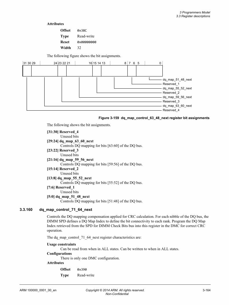
Attributes
Offset 0x38C
Type Read-writeReset 0x00000000
Width 32
The following figure shows the bit assignments.
31 30 29 24 23 22 21 16 15 14 13 8 7 6 5 0
dq_map_55_52_nextReserved_1dq_map_51_48_next
Reserved_2dq_map_59_56_next
Reserved_4dq_map_63_60_nextReserved_3
Figure 3-159 dq_map_control_63_48_next register bit assignments
The following shows the bit assignments.
[31:30] Reserved_4Unused bits
[29:24] dq_map_63_60_nextControls DQ mapping for bits [63:60] of the DQ bus.
[23:22] Reserved_3Unused bits
[21:16] dq_map_59_56_nextControls DQ mapping for bits [59:56] of the DQ bus.
[15:14] Reserved_2Unused bits
[13:8] dq_map_55_52_nextControls DQ mapping for bits [55:52] of the DQ bus.
[7:6] Reserved_1Unused bits
[5:0] dq_map_51_48_nextControls DQ mapping for bits [51:48] of the DQ bus.
3.3.160 dq_map_control_71_64_next
Controls the DQ mapping compensation applied for CRC calculation. For each nibble of the DQ bus, theDIMM SPD defines a DQ Map Index to define the bit connectivity to each rank. Program the DQ MapIndex retrieved from the SPD for DIMM Check Bits bus into this register in the DMC for correct CRCoperation.
The dq_map_control_71_64_next register characteristics are:
Usage constraintsCan be read from when in ALL states. Can be written to when in ALL states.
ConfigurationsThere is only one DMC configuration.
Attributes
Offset 0x390
Type Read-write
3 Programmers Model3.3 Register descriptions
ARM 100000_0001_00_en Copyright © 2014 ARM. All rights reserved. 3-164Non-Confidential

Reset 0x00000000
Width 32
The following figure shows the bit assignments.
31 24 23 16 15 14 13 8 7 6 5 0
Reserved_3
dq_map_71_68_nextReserved_1dq_map_67_64_next
Reserved_2rank_dq_bit_swap_next
Figure 3-160 dq_map_control_71_64_next register bit assignments
The following shows the bit assignments.
[31:24] Reserved_3Unused bits
[23:16] rank_dq_bit_swap_nextEach bit determines if the DQ bus has bit swapping as per the DDR4 RDIMM DesignSpecification applied to the corresponding rank. Normally, this bit must be set high for oddphysical ranks.
[15:14] Reserved_2Unused bits
[13:8] dq_map_71_68_nextControls DQ mapping for bits [71:68] of the DQ bus. This corresponds to CB [7:4] on theDIMM.
[7:6] Reserved_1Unused bits
[5:0] dq_map_67_64_nextControls DQ mapping for bits [67:64] of the DQ bus. This corresponds to CB [3:0] on theDIMM.
3.3.161 rank_status
Shows the current status of geardown, MPD and CAL.
The rank_status register characteristics are:
Usage constraintsCan be read from when in ALL states. Cannot be changed.
ConfigurationsThere is only one DMC configuration.
Attributes
Offset 0x398
Type Read-onlyReset 0x00000000
Width 32
The following figure shows the bit assignments.
3 Programmers Model3.3 Register descriptions
ARM 100000_0001_00_en Copyright © 2014 ARM. All rights reserved. 3-165Non-Confidential

31 24 23 16 15 8 7 0
m0_rank_cal_modeReserved_1
m0_rank_mpd_modem0_rank_geardown_mode
Figure 3-161 rank_status register bit assignments
The following shows the bit assignments.
[31:24] Reserved_1Unused bits
[23:16] m0_rank_cal_modeOne-bit per rank indicating if the rank is in CAL mode
[15:8] m0_rank_mpd_modeOne-bit per rank indicating if the rank is in MPD mode
[7:0] m0_rank_geardown_modeOne-bit per rank indicating if the rank is in geardown mode
3.3.162 mode_change_status
Shows the current status of the sequence that is currently being processed.
The mode_change_status register characteristics are:
Usage constraintsCan be read from when in ALL states. Cannot be changed.
ConfigurationsThere is only one DMC configuration.
Attributes
Offset 0x39C
Type Read-onlyReset 0x00000000
Width 32
The following figure shows the bit assignments.
31 18 17 16 15 12 11 4 3 2 0
Reserved_3
m0_mode_change_ranksReserved_1m0_mode_change_cmd
Reserved_2m0_mode_change_seq
Figure 3-162 mode_change_status register bit assignments
The following shows the bit assignments.
[31:18] Reserved_3Unused bits
[17:16] m0_mode_change_seqThe sequence position the mode change is performing.
[15:12] Reserved_2Unused bits
[11:4] m0_mode_change_ranksOne-bit per rank indicating the ranks being targetted by the command.
3 Programmers Model3.3 Register descriptions
ARM 100000_0001_00_en Copyright © 2014 ARM. All rights reserved. 3-166Non-Confidential
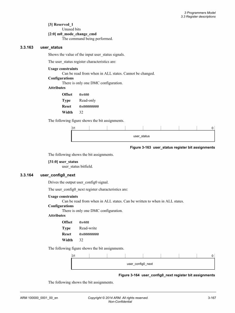
[3] Reserved_1Unused bits
[2:0] m0_mode_change_cmdThe command being performed.
3.3.163 user_status
Shows the value of the input user_status signals.
The user_status register characteristics are:
Usage constraintsCan be read from when in ALL states. Cannot be changed.
ConfigurationsThere is only one DMC configuration.
Attributes
Offset 0x400
Type Read-onlyReset 0x00000000
Width 32
The following figure shows the bit assignments.
31 0
user_status
Figure 3-163 user_status register bit assignments
The following shows the bit assignments.
[31:0] user_statususer_status bitfield.
3.3.164 user_config0_next
Drives the output user_config0 signal.
The user_config0_next register characteristics are:
Usage constraintsCan be read from when in ALL states. Can be written to when in ALL states.
ConfigurationsThere is only one DMC configuration.
Attributes
Offset 0x408
Type Read-writeReset 0x00000000
Width 32
The following figure shows the bit assignments.
31 0
user_config0_next
Figure 3-164 user_config0_next register bit assignments
The following shows the bit assignments.
3 Programmers Model3.3 Register descriptions
ARM 100000_0001_00_en Copyright © 2014 ARM. All rights reserved. 3-167Non-Confidential

[31:0] user_config0_nextuser_config0_next bitfield.
3.3.165 user_config1_next
Drives the output user_config1 signal.
The user_config1_next register characteristics are:
Usage constraintsCan be read from when in ALL states. Can be written to when in ALL states.
ConfigurationsThere is only one DMC configuration.
Attributes
Offset 0x40C
Type Read-writeReset 0x00000000
Width 32
The following figure shows the bit assignments.
31 0
user_config1_next
Figure 3-165 user_config1_next register bit assignments
The following shows the bit assignments.
[31:0] user_config1_nextuser_config1_next bitfield.
3.3.166 user_config2
Drives the output user_config2 signal.
The user_config2 register characteristics are:
Usage constraintsCan be read from when in ALL states. Can be written to when in ALL states.
ConfigurationsThere is only one DMC configuration.
Attributes
Offset 0x410
Type Read-writeReset 0x00000000
Width 32
The following figure shows the bit assignments.
31 0
user_config2
Figure 3-166 user_config2 register bit assignments
The following shows the bit assignments.
[31:0] user_config2user_config2 bitfield.
3 Programmers Model3.3 Register descriptions
ARM 100000_0001_00_en Copyright © 2014 ARM. All rights reserved. 3-168Non-Confidential

3.3.167 user_config3
Drives the output user_config3 signal.
The user_config3 register characteristics are:
Usage constraintsCan be read from when in ALL states. Can be written to when in ALL states.
ConfigurationsThere is only one DMC configuration.
Attributes
Offset 0x414
Type Read-writeReset 0x00000000
Width 32
The following figure shows the bit assignments.
31 0
user_config3
Figure 3-167 user_config3 register bit assignments
The following shows the bit assignments.
[31:0] user_config3user_config3 bitfield.
3.3.168 interrupt_control
Configures interrupt behavior.
The interrupt_control register characteristics are:
Usage constraintsCan be read from when in ALL states. Can be written to when in ALL states.
ConfigurationsThere is only one DMC configuration.
Attributes
Offset 0x500
Type Read-writeReset 0x00000000
Width 32
The following figure shows the bit assignments.
3 Programmers Model3.3 Register descriptions
ARM 100000_0001_00_en Copyright © 2014 ARM. All rights reserved. 3-169Non-Confidential

31 10 9 8 7 6 5 4 3 2 1 0
Reserved_1
dram_ecc_errc_int_enram_ecc_errd_int_enram_ecc_errc_int_en
dram_ecc_errd_int_enfailed_access_int_en
temperature_event_int_enlink_err_int_enfailed_prog_int_en
phy_request_int_enarch_fsm_int_en
Figure 3-168 interrupt_control register bit assignments
The following shows the bit assignments.
[31:10] Reserved_1Unused bits
[9] phy_request_int_enProgram to enable or disable the PHY request interrupt.
[8] arch_fsm_int_enProgram to enable or disable the architectural fsm interrupt.
[7] temperature_event_int_enProgram to enable or disable the temperature event interrupt.
[6] link_err_int_enProgram to enable or disable the link error interrupt.
[5] failed_prog_int_enProgram to enable or disable the failed programmer's access interrupt.
[4] failed_access_int_enProgram to enable or disable the failed system access interrupt.
[3] dram_ecc_errd_int_enProgram to enable or disable the dram uncorrected error interrupt.
[2] dram_ecc_errc_int_enProgram to enable or disable the dram corrected error interrupt.
[1] ram_ecc_errd_int_enProgram to enable or disable the ram uncorrected error interrupt.
[0] ram_ecc_errc_int_enProgram to enable or disable the ram corrected error interrupt.
3.3.169 interrupt_clr
Clear register for interrupts.
The interrupt_clr register characteristics are:
Usage constraintsCannot be read from. Can be written to when in ALL states.
ConfigurationsThere is only one DMC configuration.
Attributes
Offset 0x508
Type Write-onlyReset 0x00000000
Width 32
The following figure shows the bit assignments.
3 Programmers Model3.3 Register descriptions
ARM 100000_0001_00_en Copyright © 2014 ARM. All rights reserved. 3-170Non-Confidential

31 10 9 8 7 6 5 4 3 2 1 0
Reserved_1
dram_ecc_errc_int_clrram_ecc_errd_int_clrram_ecc_errc_int_clr
dram_ecc_errd_int_clrfailed_access_int_clr
temperature_event_int_clrlink_err_int_clrfailed_prog_int_clr
phy_request_int_clrarch_fsm_int_clr
Figure 3-169 interrupt_clr register bit assignments
The following shows the bit assignments.
[31:10] Reserved_1Unused bits
[9] phy_request_int_clrProgram to clear the PHY request interrupt.
[8] arch_fsm_int_clrProgram to clear the architectural fsm interrupt.
[7] temperature_event_int_clrProgram to clear the temperature event interrupt.
[6] link_err_int_clrProgram to clear the link error interrupt.
[5] failed_prog_int_clrProgram to clear the failed programmer's access interrupt.
[4] failed_access_int_clrProgram to clear the failed system access interrupt.
[3] dram_ecc_errd_int_clrProgram to clear the dram uncorrected error interrupt.
[2] dram_ecc_errc_int_clrProgram to clear the dram corrected error interrupt.
[1] ram_ecc_errd_int_clrProgram to clear the ram uncorrected error interrupt.
[0] ram_ecc_errc_int_clrProgram to clear the ram corrected error interrupt.
3.3.170 interrupt_status
Status register for interrupts (pre-mask).
The interrupt_status register characteristics are:
Usage constraintsCan be read from when in ALL states. Cannot be changed.
ConfigurationsThere is only one DMC configuration.
Attributes
Offset 0x510
Type Read-onlyReset 0x00000000
Width 32
The following figure shows the bit assignments.
3 Programmers Model3.3 Register descriptions
ARM 100000_0001_00_en Copyright © 2014 ARM. All rights reserved. 3-171Non-Confidential

31 26 25 24 23 22 21 20 19 18 17 16 15 10 9 8 7 6 5 4 3 2 1 0
Reserved_1Reserved_2
dram_ecc_errc_int_statusram_ecc_errd_int_statusram_ecc_errc_int_status
dram_ecc_errd_int_statusfailed_access_int_status
temperature_event_int_statuslink_err_int_statusfailed_prog_int_status
ram_ecc_errc_int_overflow_statusphy_request_int_statusarch_fsm_int_status
ram_ecc_errd_int_overflow_statusdram_ecc_errc_int_overflow_status
failed_prog_int_overflow_statusfailed_access_int_overflow_statusdram_ecc_errd_int_overflow_status
arch_fsm_int_overflow_statustemperature_event_int_overflow_statuslink_err_int_overflow_status
phy_request_int_overflow_status
Figure 3-170 interrupt_status register bit assignments
The following shows the bit assignments.
[31:26] Reserved_2Unused bits
[25] phy_request_int_overflow_statusShows the status of the PHY request interrupt overflow.
[24] arch_fsm_int_overflow_statusShows the status of the architectural fsm interrupt overflow.
[23] temperature_event_int_overflow_statusShows the status of the link failure interrupt overflow.
[22] link_err_int_overflow_statusShows the status of the link error interrupt overflow.
[21] failed_prog_int_overflow_statusShows the status of the failed programmer's access interrupt overflow.
[20] failed_access_int_overflow_statusShows the status of the failed system access interrupt overflow.
[19] dram_ecc_errd_int_overflow_statusShows the status of the DRAM uncorrected error interrupt overflow.
[18] dram_ecc_errc_int_overflow_statusShows the status of the DRAM corrected error interrupt overflow.
[17] ram_ecc_errd_int_overflow_statusShows the status of the RAM uncorrected error interrupt overflow.
[16] ram_ecc_errc_int_overflow_statusShows the status of the RAM corrected error interrupt overflow.
[15:10] Reserved_1Unused bits
[9] phy_request_int_statusShows the status of the PHY request interrupt.
[8] arch_fsm_int_statusShows the status of the architectural fsm interrupt.
[7] temperature_event_int_statusShows the status of the temperature event interrupt.
3 Programmers Model3.3 Register descriptions
ARM 100000_0001_00_en Copyright © 2014 ARM. All rights reserved. 3-172Non-Confidential

[6] link_err_int_statusShows the status of the link error interrupt.
[5] failed_prog_int_statusShows the status of the failed programmer's access interrupt.
[4] failed_access_int_statusShows the status of the failed system access interrupt.
[3] dram_ecc_errd_int_statusShows the status of the DRAM uncorrected error interrupt.
[2] dram_ecc_errc_int_statusShows the status of the DRAM corrected error interrupt.
[1] ram_ecc_errd_int_statusShows the status of the RAM uncorrected error interrupt.
[0] ram_ecc_errc_int_statusShows the status of the RAM corrected error interrupt.
3.3.171 ram_ecc_errc_int_info_31_00
Shows information relating to the interrupt
The ram_ecc_errc_int_info_31_00 register characteristics are:
Usage constraintsCan be read from when in ALL states. Cannot be changed.
ConfigurationsThere is only one DMC configuration.
Attributes
Offset 0x518
Type Read-onlyReset 0x00000000
Width 32
The following figure shows the bit assignments.
31 29 28 11 10 1 0
ram_ecc_errc_int_info_row
ram_ecc_errc_int_info_rankram_ecc_errc_int_info_columnram_ecc_errc_int_info_30_00_valid
Figure 3-171 ram_ecc_errc_int_info_31_00 register bit assignments
The following shows the bit assignments.
[31:29] ram_ecc_errc_int_info_rankRank.
[28:11] ram_ecc_errc_int_info_rowRow.
[10:1] ram_ecc_errc_int_info_columnColumn.
[0] ram_ecc_errc_int_info_30_00_validIndicates if an overflow (single interrupt overflow, or multiple interrupt overflow) has occurredand whether the interrupt information is valid. 1 indicates it is valid and that no overflow hasoccurred.
3 Programmers Model3.3 Register descriptions
ARM 100000_0001_00_en Copyright © 2014 ARM. All rights reserved. 3-173Non-Confidential

3.3.172 ram_ecc_errc_int_info_63_32
Shows information relating to the interrupt
The ram_ecc_errc_int_info_63_32 register characteristics are:
Usage constraintsCan be read from when in ALL states. Cannot be changed.
ConfigurationsThere is only one DMC configuration.
Attributes
Offset 0x51C
Type Read-onlyReset 0x00000000
Width 32
The following figure shows the bit assignments.
31 30 11 10 4 3 0
Reserved_1
ram_ecc_errc_int_info_61_31_validram_ecc_errc_int_info_dbidram_ecc_errc_int_info_bank
Figure 3-172 ram_ecc_errc_int_info_63_32 register bit assignments
The following shows the bit assignments.
[31] ram_ecc_errc_int_info_61_31_validIndicates if an overflow (single interrupt overflow, or multiple interrupt overflow) has occurredand whether the interrupt information is valid. 1 indicates it is valid and that no overflow hasoccurred.
[30:11] Reserved_1Unused bits
[10:4] ram_ecc_errc_int_info_dbidData Buffer ID.
[3:0] ram_ecc_errc_int_info_bankBank.
3.3.173 ram_ecc_errd_int_info_31_00
Shows information relating to the interrupt
The ram_ecc_errd_int_info_31_00 register characteristics are:
Usage constraintsCan be read from when in ALL states. Cannot be changed.
ConfigurationsThere is only one DMC configuration.
Attributes
Offset 0x520
Type Read-onlyReset 0x00000000
Width 32
The following figure shows the bit assignments.
3 Programmers Model3.3 Register descriptions
ARM 100000_0001_00_en Copyright © 2014 ARM. All rights reserved. 3-174Non-Confidential
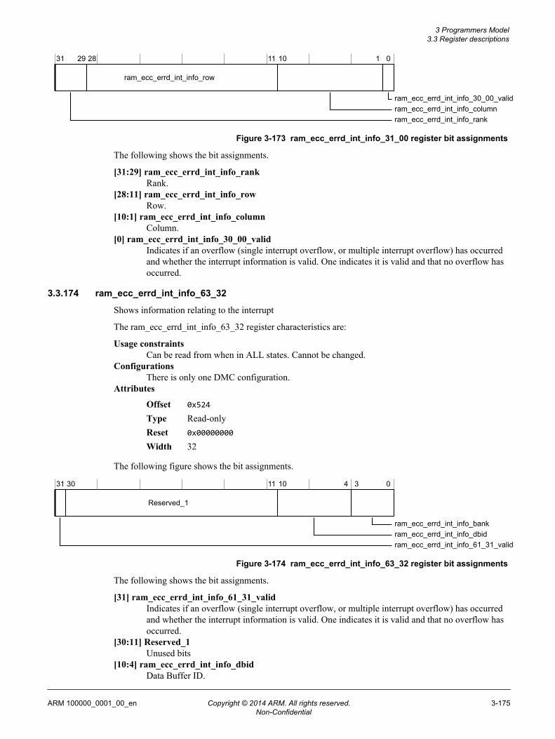
31 29 28 11 10 1 0
ram_ecc_errd_int_info_row
ram_ecc_errd_int_info_rankram_ecc_errd_int_info_columnram_ecc_errd_int_info_30_00_valid
Figure 3-173 ram_ecc_errd_int_info_31_00 register bit assignments
The following shows the bit assignments.
[31:29] ram_ecc_errd_int_info_rankRank.
[28:11] ram_ecc_errd_int_info_rowRow.
[10:1] ram_ecc_errd_int_info_columnColumn.
[0] ram_ecc_errd_int_info_30_00_validIndicates if an overflow (single interrupt overflow, or multiple interrupt overflow) has occurredand whether the interrupt information is valid. One indicates it is valid and that no overflow hasoccurred.
3.3.174 ram_ecc_errd_int_info_63_32
Shows information relating to the interrupt
The ram_ecc_errd_int_info_63_32 register characteristics are:
Usage constraintsCan be read from when in ALL states. Cannot be changed.
ConfigurationsThere is only one DMC configuration.
Attributes
Offset 0x524
Type Read-onlyReset 0x00000000
Width 32
The following figure shows the bit assignments.
31 30 11 10 4 3 0
Reserved_1
ram_ecc_errd_int_info_61_31_validram_ecc_errd_int_info_dbidram_ecc_errd_int_info_bank
Figure 3-174 ram_ecc_errd_int_info_63_32 register bit assignments
The following shows the bit assignments.
[31] ram_ecc_errd_int_info_61_31_validIndicates if an overflow (single interrupt overflow, or multiple interrupt overflow) has occurredand whether the interrupt information is valid. One indicates it is valid and that no overflow hasoccurred.
[30:11] Reserved_1Unused bits
[10:4] ram_ecc_errd_int_info_dbidData Buffer ID.
3 Programmers Model3.3 Register descriptions
ARM 100000_0001_00_en Copyright © 2014 ARM. All rights reserved. 3-175Non-Confidential

[3:0] ram_ecc_errd_int_info_bankBank.
3.3.175 dram_ecc_errc_int_info_31_00
Shows information relating to the interrupt
The dram_ecc_errc_int_info_31_00 register characteristics are:
Usage constraintsCan be read from when in ALL states. Cannot be changed.
ConfigurationsThere is only one DMC configuration.
Attributes
Offset 0x528
Type Read-onlyReset 0x00000000
Width 32
The following figure shows the bit assignments.
31 29 28 11 10 1 0
dram_ecc_errc_int_info_row
dram_ecc_errc_int_info_rankdram_ecc_errc_int_info_columndram_ecc_errc_int_info_30_00_valid
Figure 3-175 dram_ecc_errc_int_info_31_00 register bit assignments
The following shows the bit assignments.
[31:29] dram_ecc_errc_int_info_rankRank.
[28:11] dram_ecc_errc_int_info_rowRow.
[10:1] dram_ecc_errc_int_info_columnColumn.
[0] dram_ecc_errc_int_info_30_00_validIndicates if an overflow (single interrupt overflow, or multiple interrupt overflow) has occurredand whether the interrupt information is valid. One indicates it is valid and that no overflow hasoccurred.
3.3.176 dram_ecc_errc_int_info_63_32
Shows information relating to the interrupt
The dram_ecc_errc_int_info_63_32 register characteristics are:
Usage constraintsCan be read from when in ALL states. Cannot be changed.
ConfigurationsThere is only one DMC configuration.
Attributes
Offset 0x52C
Type Read-onlyReset 0x00000000
Width 32
3 Programmers Model3.3 Register descriptions
ARM 100000_0001_00_en Copyright © 2014 ARM. All rights reserved. 3-176Non-Confidential

The following figure shows the bit assignments.
31 30 28 27 24 23 4 3 0
dram_ecc_errc_int_info_err_loc
Reserved_1dram_ecc_errc_int_info_err_loc_validdram_ecc_errc_int_info_bank
dram_ecc_errc_int_info_61_31_valid
Figure 3-176 dram_ecc_errc_int_info_63_32 register bit assignments
The following shows the bit assignments.
[31] dram_ecc_errc_int_info_61_31_validIndicates if an overflow (single interrupt overflow, or multiple interrupt overflow) has occurredand whether the interrupt information is valid. 1 indicates it is valid and that no overflow hasoccurred.
[30:28] Reserved_1Unused bits
[27:24] dram_ecc_errc_int_info_err_loc_validError location valid.
[23:4] dram_ecc_errc_int_info_err_locError location containing 4 sets of 5-bit nibble locations indicating which of the 18 possiblenibble locations (0..17) each error was found in.
[3:0] dram_ecc_errc_int_info_bankBank.
3.3.177 dram_ecc_errd_int_info_31_00
Shows information relating to the interrupt
The dram_ecc_errd_int_info_31_00 register characteristics are:
Usage constraintsCan be read from when in ALL states. Cannot be changed.
ConfigurationsThere is only one DMC configuration.
Attributes
Offset 0x530
Type Read-onlyReset 0x00000000
Width 32
The following figure shows the bit assignments.
31 29 28 11 10 1 0
dram_ecc_errd_int_info_row
dram_ecc_errd_int_info_rankdram_ecc_errd_int_info_columndram_ecc_errd_int_info_30_00_valid
Figure 3-177 dram_ecc_errd_int_info_31_00 register bit assignments
The following shows the bit assignments.
[31:29] dram_ecc_errd_int_info_rankRank.
3 Programmers Model3.3 Register descriptions
ARM 100000_0001_00_en Copyright © 2014 ARM. All rights reserved. 3-177Non-Confidential

[28:11] dram_ecc_errd_int_info_rowRow.
[10:1] dram_ecc_errd_int_info_columnColumn.
[0] dram_ecc_errd_int_info_30_00_validIndicates if an overflow (single interrupt overflow, or multiple interrupt overflow) has occurredand whether the interrupt information is valid. One indicates it is valid and that no overflow hasoccurred.
3.3.178 dram_ecc_errd_int_info_63_32
Shows information relating to the interrupt
The dram_ecc_errd_int_info_63_32 register characteristics are:
Usage constraintsCan be read from when in ALL states. Cannot be changed.
ConfigurationsThere is only one DMC configuration.
Attributes
Offset 0x534
Type Read-onlyReset 0x00000000
Width 32
The following figure shows the bit assignments.
31 30 4 3 0
Reserved_1
dram_ecc_errd_int_info_61_31_validdram_ecc_errd_int_info_bank
Figure 3-178 dram_ecc_errd_int_info_63_32 register bit assignments
The following shows the bit assignments.
[31] dram_ecc_errd_int_info_61_31_validIndicates if an overflow (single interrupt overflow, or multiple interrupt overflow) has occurredand whether the interrupt information is valid. One indicates it is valid and that no overflow hasoccurred.
[30:4] Reserved_1Unused bits
[3:0] dram_ecc_errd_int_info_bankBank.
3.3.179 failed_access_int_info_31_00
Shows information relating to the interrupt
The failed_access_int_info_31_00 register characteristics are:
Usage constraintsCan be read from when in ALL states. Cannot be changed.
ConfigurationsThere is only one DMC configuration.
Attributes
Offset 0x538
Type Read-only
3 Programmers Model3.3 Register descriptions
ARM 100000_0001_00_en Copyright © 2014 ARM. All rights reserved. 3-178Non-Confidential

Reset 0x00000000
Width 32
The following figure shows the bit assignments.
31 23 22 21 20 19 18 10 9 8 7 1 0
Reserved_1
failed_access_int_info_nsfailed_access_int_info_source_idfailed_access_int_info_30_00_valid
failed_access_int_info_writefailed_access_int_info_source_region
failed_access_int_info_unmappedfailed_access_int_tz_failfailed_access_int_info_outside_default
failed_access_int_info_rank_masked
Figure 3-179 failed_access_int_info_31_00 register bit assignments
The following shows the bit assignments.
[31:23] Reserved_1Unused bits
[22] failed_access_int_info_rank_maskedAccess to a masked rank.
[21] failed_access_int_info_unmappedAccess to an unmapped (reserved) system address location.
[20] failed_access_int_tz_failAccess failed the security checks of the matching regions
[19] failed_access_int_info_outside_defaultAccess to a memory address location greater than the maximum address of the default region
[18:10] failed_access_int_info_source_regionAddress region of the failed access. The lower 8 bits map to address regions 0 to 7. The upperbit maps to the default region.
[9] failed_access_int_info_writeDirection of the failed access. When HIGH the access is a write.
[8] failed_access_int_info_nsSecurity setting of the failed access. When HIGH the access is Non-secure.
[7:1] failed_access_int_info_source_idSource ID of the failed access
[0] failed_access_int_info_30_00_validIndicates if an overflow (single interrupt overflow, or multiple interrupt overflow) has occurredand whether the interrupt information is valid. One indicates it is valid and that no overflow hasoccurred.
3.3.180 failed_access_int_info_63_32
Shows information relating to the interrupt
The failed_access_int_info_63_32 register characteristics are:
Usage constraintsCan be read from when in ALL states. Cannot be changed.
ConfigurationsThere is only one DMC configuration.
Attributes
Offset 0x53C
3 Programmers Model3.3 Register descriptions
ARM 100000_0001_00_en Copyright © 2014 ARM. All rights reserved. 3-179Non-Confidential

Type Read-onlyReset 0x00000000
Width 32
The following figure shows the bit assignments.
31 30 0
Reserved_1
failed_access_int_info_61_31_valid
Figure 3-180 failed_access_int_info_63_32 register bit assignments
The following shows the bit assignments.
[31] failed_access_int_info_61_31_validIndicates if an overflow (single interrupt overflow, or multiple interrupt overflow) has occurredand whether the interrupt information is valid. One indicates it is valid and that no overflow hasoccurred.
[30:0] Reserved_1Unused bits
3.3.181 failed_prog_int_info_31_00
Shows information relating to the interrupt
The failed_prog_int_info_31_00 register characteristics are:
Usage constraintsCan be read from when in ALL states. Cannot be changed.
ConfigurationsThere is only one DMC configuration.
Attributes
Offset 0x540
Type Read-onlyReset 0x00000000
Width 32
The following figure shows the bit assignments.
31 14 13 1 0
failed_prog_int_info_addressReserved_1
failed_prog_int_info_30_00_valid
Figure 3-181 failed_prog_int_info_31_00 register bit assignments
The following shows the bit assignments.
[31:14] Reserved_1Unused bits
[13:1] failed_prog_int_info_addressRegister address (paddr[12:0]).
[0] failed_prog_int_info_30_00_validIndicates if an overflow (single interrupt overflow, or multiple interrupt overflow) has occurredand whether the interrupt information is valid. One indicates it is valid and that no overflow hasoccurred.
3 Programmers Model3.3 Register descriptions
ARM 100000_0001_00_en Copyright © 2014 ARM. All rights reserved. 3-180Non-Confidential

3.3.182 failed_prog_int_info_63_32
Shows information relating to the interrupt
The failed_prog_int_info_63_32 register characteristics are:
Usage constraintsCan be read from when in ALL states. Cannot be changed.
ConfigurationsThere is only one DMC configuration.
Attributes
Offset 0x544
Type Read-onlyReset 0x00000000
Width 32
The following figure shows the bit assignments.
31 30 0
Reserved_1
failed_prog_int_info_61_31_valid
Figure 3-182 failed_prog_int_info_63_32 register bit assignments
The following shows the bit assignments.
[31] failed_prog_int_info_61_31_validIndicates if an overflow (single interrupt overflow, or multiple interrupt overflow) has occurredand whether the interrupt information is valid. One indicates it is valid and that no overflow hasoccurred.
[30:0] Reserved_1Unused bits
3.3.183 link_err_int_info_31_00
Shows information relating to the interrupt
The link_err_int_info_31_00 register characteristics are:
Usage constraintsCan be read from when in ALL states. Cannot be changed.
ConfigurationsThere is only one DMC configuration.
Attributes
Offset 0x548
Type Read-onlyReset 0x00000000
Width 32
The following figure shows the bit assignments.
3 Programmers Model3.3 Register descriptions
ARM 100000_0001_00_en Copyright © 2014 ARM. All rights reserved. 3-181Non-Confidential

31 7 6 5 4 1 0
Reserved_1
link_err_int_info_errlink_err_int_infolink_err_int_info_30_00_valid
link_err_int_info_alert_n
Figure 3-183 link_err_int_info_31_00 register bit assignments
The following shows the bit assignments.
[31:7] Reserved_1Unused bits
[6] link_err_int_info_alert_nReturns the value sent on the dfi_alert_n signal.
[5] link_err_int_info_errReturns the value sent on the dfi_err signal.
[4:1] link_err_int_infoFor a dfi_err error, returns the corresponding value sent on dfi_err_info. For all other errors it isnot used.
[0] link_err_int_info_30_00_validIndicates if an overflow (single interrupt overflow, or multiple interrupt overflow) has occurredand whether the interrupt information is valid. One indicates it is valid and that no overflow hasoccurred.
3.3.184 link_err_int_info_63_32
Shows information relating to the interrupt
The link_err_int_info_63_32 register characteristics are:
Usage constraintsCan be read from when in ALL states. Cannot be changed.
ConfigurationsThere is only one DMC configuration.
Attributes
Offset 0x54C
Type Read-onlyReset 0x00000000
Width 32
The following figure shows the bit assignments.
31 30 0
Reserved_1
link_err_int_info_61_31_valid
Figure 3-184 link_err_int_info_63_32 register bit assignments
The following shows the bit assignments.
[31] link_err_int_info_61_31_validIndicates if an overflow (single interrupt overflow, or multiple interrupt overflow) has occurredand whether the interrupt information is valid. One indicates it is valid and that no overflow hasoccurred.
[30:0] Reserved_1Unused bits
3 Programmers Model3.3 Register descriptions
ARM 100000_0001_00_en Copyright © 2014 ARM. All rights reserved. 3-182Non-Confidential

3.3.185 arch_fsm_int_info_31_00
Shows information relating to the interrupt
The arch_fsm_int_info_31_00 register characteristics are:
Usage constraintsCan be read from when in ALL states. Cannot be changed.
ConfigurationsThere is only one DMC configuration.
Attributes
Offset 0x550
Type Read-onlyReset 0x00000000
Width 32
The following figure shows the bit assignments.
31 3 2 1 0
Reserved_1
arch_fsm_int_info_mgr_dci_failedarch_fsm_int_info_abortedarch_fsm_int_info_30_00_valid
Figure 3-185 arch_fsm_int_info_31_00 register bit assignments
The following shows the bit assignments.
[31:3] Reserved_1Unused bits
[2] arch_fsm_int_info_mgr_dci_failedA direct command in a previous sequence has failed.
[1] arch_fsm_int_info_abortedSignals that the transition completed cleanly or was aborted.
[0] arch_fsm_int_info_30_00_validIndicates if an overflow (single interrupt overflow, or multiple interrupt overflow) has occurredand whether the interrupt information is valid. One indicates it is valid and that no overflow hasoccurred.
3.3.186 arch_fsm_int_info_63_32
Shows information relating to the interrupt
The arch_fsm_int_info_63_32 register characteristics are:
Usage constraintsCan be read from when in ALL states. Cannot be changed.
ConfigurationsThere is only one DMC configuration.
Attributes
Offset 0x554
Type Read-onlyReset 0x00000000
Width 32
The following figure shows the bit assignments.
3 Programmers Model3.3 Register descriptions
ARM 100000_0001_00_en Copyright © 2014 ARM. All rights reserved. 3-183Non-Confidential

31 30 0
Reserved_1
arch_fsm_int_info_61_31_valid
Figure 3-186 arch_fsm_int_info_63_32 register bit assignments
The following shows the bit assignments.
[31] arch_fsm_int_info_61_31_validIndicates if an overflow (single interrupt overflow, or multiple interrupt overflow) has occurredand whether the interrupt information is valid. One indicates it is valid and that no overflow hasoccurred.
[30:0] Reserved_1Unused bits
3.3.187 integ_cfg
Integration test register to enable integration test mode.
The integ_cfg register characteristics are:
Usage constraintsCan be read from when in ALL states. Can be written to when in CONFIG or LOW-POWERstates.
ConfigurationsThere is only one DMC configuration.
Attributes
Offset 0xE00
Type Read-writeReset 0x00000000
Width 32
The following figure shows the bit assignments.
31 1 0
Reserved_1
integ_test_en
Figure 3-187 integ_cfg register bit assignments
The following shows the bit assignments.
[31:1] Reserved_1Unused bits
[0] integ_test_eninteg_test_en bitfield. The supported range for this bitfield is 0-1.
3.3.188 integ_outputs
Drives the value of outputs when in integration test mode.
The integ_outputs register characteristics are:
Usage constraintsCannot be read from. Can be written to when in CONFIG or LOW-POWER states.
ConfigurationsThere is only one DMC configuration.
Attributes
3 Programmers Model3.3 Register descriptions
ARM 100000_0001_00_en Copyright © 2014 ARM. All rights reserved. 3-184Non-Confidential

Offset 0xE08
Type Write-onlyReset 0x00000000
Width 32
The following figure shows the bit assignments.
31 30 29 28 27 26 25 24 23 22 21 20 19 18 17 16 15 14 13 12 11 10 9 8 7 6 5 4 3 2 1 0
ram_ecc_errd_int_integram_ecc_errc_oflow_integram_ecc_errc_int_integ
ram_ecc_errd_oflow_integdram_ecc_errc_int_integ
dram_ecc_errd_oflow_integdram_ecc_errd_int_integdram_ecc_errc_oflow_integ
failed_prog_int_integfailed_access_oflow_integfailed_access_int_integ
failed_prog_oflow_integlink_err_int_integ
temperature_event_oflow_integtemperature_event_int_integlink_err_oflow_integ
phy_request_int_integarch_fsm_oflow_integarch_fsm_int_integ
phy_request_oflow_integdirect_cmd_event_out0_integ
direct_cmd_event_out3_integdirect_cmd_event_out2_integdirect_cmd_event_out1_integ
scrub_event_out2_integscrub_event_out1_integscrub_event_out0_integ
scrub_event_out3_integscrub_event_out4_integ
scrub_event_out7_integscrub_event_out6_integscrub_event_out5_integ
Figure 3-188 integ_outputs register bit assignments
The following shows the bit assignments.
[31] scrub_event_out7_integscrub_event_out7_integ bitfield.
[30] scrub_event_out6_integscrub_event_out6_integ bitfield.
[29] scrub_event_out5_integscrub_event_out5_integ bitfield.
[28] scrub_event_out4_integscrub_event_out4_integ bitfield.
[27] scrub_event_out3_integscrub_event_out3_integ bitfield.
3 Programmers Model3.3 Register descriptions
ARM 100000_0001_00_en Copyright © 2014 ARM. All rights reserved. 3-185Non-Confidential

[26] scrub_event_out2_integscrub_event_out2_integ bitfield.
[25] scrub_event_out1_integscrub_event_out1_integ bitfield.
[24] scrub_event_out0_integscrub_event_out0_integ bitfield.
[23] direct_cmd_event_out3_integdirect_cmd_event_out3_integ bitfield.
[22] direct_cmd_event_out2_integdirect_cmd_event_out2_integ bitfield.
[21] direct_cmd_event_out1_integdirect_cmd_event_out1_integ bitfield.
[20] direct_cmd_event_out0_integdirect_cmd_event_out0_integ bitfield.
[19] phy_request_oflow_integphy_request_oflow_integ bitfield.
[18] phy_request_int_integphy_request_int_integ bitfield.
[17] arch_fsm_oflow_integarch_fsm_oflow_integ bitfield.
[16] arch_fsm_int_integarch_fsm_int_integ bitfield.
[15] temperature_event_oflow_integtemperature_event_oflow_integ bitfield.
[14] temperature_event_int_integtemperature_event_int_integ bitfield.
[13] link_err_oflow_integlink_err_oflow_integ bitfield.
[12] link_err_int_integlink_err_int_integ bitfield.
[11] failed_prog_oflow_integfailed_prog_oflow_integ bitfield.
[10] failed_prog_int_integfailed_prog_int_integ bitfield.
[9] failed_access_oflow_integfailed_access_oflow_integ bitfield.
[8] failed_access_int_integfailed_access_int_integ bitfield.
[7] dram_ecc_errd_oflow_integdram_ecc_errd_oflow_integ bitfield.
[6] dram_ecc_errd_int_integdram_ecc_errd_int_integ bitfield.
[5] dram_ecc_errc_oflow_integdram_ecc_errc_oflow_integ bitfield.
[4] dram_ecc_errc_int_integdram_ecc_errc_int_integ bitfield.
[3] ram_ecc_errd_oflow_integram_ecc_errd_oflow_integ bitfield.
[2] ram_ecc_errd_int_integram_ecc_errd_int_integ bitfield.
[1] ram_ecc_errc_oflow_integram_ecc_errc_oflow_integ bitfield.
[0] ram_ecc_errc_int_integram_ecc_errc_int_integ bitfield.
3 Programmers Model3.3 Register descriptions
ARM 100000_0001_00_en Copyright © 2014 ARM. All rights reserved. 3-186Non-Confidential

3.3.189 address_control_now
Configures the DRAM address parameters. Use the DRAM device data sheet or Serial Presence Detect(SPD)-derived values to assist in programming these values.
The address_control_now register characteristics are:
Usage constraintsCan be read from when in ALL states. Cannot be written to and only updated when in CONFIGor LOW-POWER states.
ConfigurationsThere is only one DMC configuration.
Attributes
Offset 0x1010
Type Read-onlyReset 0x00030202
Width 32
The following figure shows the bit assignments.
31 29 28 27 26 25 24 23 19 18 16 15 11 10 8 7 3 2 0
Reserved_1Reserved_2Reserved_3
bank_bits_nowrow_bits_nowcolumn_bits_now
rank_bits_nowReserved_4
Reserved_5bank_hash_enable_now
Figure 3-189 address_control_now register bit assignments
The following shows the bit assignments.
[31:29] Reserved_5Unused bits
[28] bank_hash_enable_nowConfigures the bank hash function used in system address decode. Used to alter trafficdistribution across banks.
[27:26] Reserved_4Unused bits
[25:24] rank_bits_nowProgram to match the number of active ranks to be addressed.
[23:19] Reserved_3Unused bits
[18:16] bank_bits_nowProgram to match the number of banks per chip-select (rank) on the attached DRAM device.
Note
This number corresponds to the sum total of all banks in all bank groups (where applicable) on adevice.
[15:11] Reserved_2Unused bits
[10:8] row_bits_nowProgram to match the number of row bits on the attached DRAM device.
3 Programmers Model3.3 Register descriptions
ARM 100000_0001_00_en Copyright © 2014 ARM. All rights reserved. 3-187Non-Confidential

[7:3] Reserved_1Unused bits
[2:0] column_bits_nowProgram to match the number of column address bits present on the DRAM device.
3.3.190 decode_control_now
Configures how the DRAM address is decoded from the system address. The DRAM address consists ofthe rank, bank, row address, and the column address.
The decode_control_now register characteristics are:
Usage constraintsCan be read from when in ALL states. Cannot be written to and only updated when in CONFIGor LOW-POWER states.
ConfigurationsThere is only one DMC configuration.
Attributes
Offset 0x1014
Type Read-onlyReset 0x00000000
Width 32
The following figure shows the bit assignments.
31 7 6 4 3 2 1 0
Reserved_2
stripe_decode_nowReserved_1address_decode_now
Figure 3-190 decode_control_now register bit assignments
The following shows the bit assignments.
[31:7] Reserved_2Unused bits
[6:4] stripe_decode_nowDetermines the address boundary on which to stripe system requests across DRAM pages. TheDMC decodes the bottom two page address bits from a programmable slice within the lowest 14bits of the system address. To disable sub-page striping you must program this value to theDRAM page size (or use the default value 0).
Note
You must not program the DMC to stripe at a higher boundary than the DRAM page size.
[3:2] Reserved_1Unused bits
[1:0] address_decode_nowDetermines in which pattern the DRAM address components are decoded from the systemaddress.
3.3.191 address_map_now
Configures the system address mapping options.
The address_map_now register characteristics are:
3 Programmers Model3.3 Register descriptions
ARM 100000_0001_00_en Copyright © 2014 ARM. All rights reserved. 3-188Non-Confidential
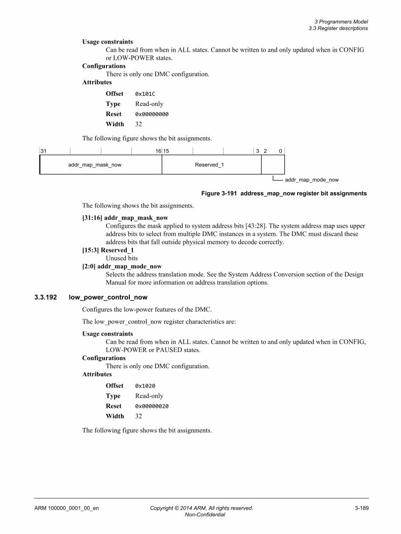
Usage constraintsCan be read from when in ALL states. Cannot be written to and only updated when in CONFIGor LOW-POWER states.
ConfigurationsThere is only one DMC configuration.
Attributes
Offset 0x101C
Type Read-onlyReset 0x00000000
Width 32
The following figure shows the bit assignments.
31 16 15 3 2 0
Reserved_1addr_map_mask_now
addr_map_mode_now
Figure 3-191 address_map_now register bit assignments
The following shows the bit assignments.
[31:16] addr_map_mask_nowConfigures the mask applied to system address bits [43:28]. The system address map uses upperaddress bits to select from multiple DMC instances in a system. The DMC must discard theseaddress bits that fall outside physical memory to decode correctly.
[15:3] Reserved_1Unused bits
[2:0] addr_map_mode_nowSelects the address translation mode. See the System Address Conversion section of the DesignManual for more information on address translation options.
3.3.192 low_power_control_now
Configures the low-power features of the DMC.
The low_power_control_now register characteristics are:
Usage constraintsCan be read from when in ALL states. Cannot be written to and only updated when in CONFIG,LOW-POWER or PAUSED states.
ConfigurationsThere is only one DMC configuration.
Attributes
Offset 0x1020
Type Read-onlyReset 0x00000020
Width 32
The following figure shows the bit assignments.
3 Programmers Model3.3 Register descriptions
ARM 100000_0001_00_en Copyright © 2014 ARM. All rights reserved. 3-189Non-Confidential

31 8 7 4 3 2 1 0
Reserved_2
auto_power_down_nowstop_mem_clock_sref_nowReserved_1
auto_self_refresh_nowasr_period_now
Figure 3-192 low_power_control_now register bit assignments
The following shows the bit assignments.
[31:8] Reserved_2Unused bits
[7:4] asr_period_nowProgram the number of tREFI intervals to wait without activity before placing the DRAM into aself-refresh state when auto_self_refresh is enabled. The supported range for this bitfield is1-15.
[3] auto_self_refresh_nowProgram to enable or disable placing a DRAM rank into a self-refresh state when the rank hasbeen idle for the amount of time that asr_period defines.
[2] auto_power_down_nowProgram to enable or disable placing the DRAM into a power-down state when idle.
[1] stop_mem_clock_sref_nowProgram to enable or disable stopping the DRAM clock when the memory device is in self-refresh, reset, or maximum power down.
[0] Reserved_1Unused bits
3.3.193 turnaround_control_now
Configures the settings for arbitration between read and write and rank to rank traffic on the DRAM bus.
The turnaround_control_now register characteristics are:
Usage constraintsCan be read from when in ALL states. Cannot be written to and only updated when in CONFIG,LOW-POWER or PAUSED states.
ConfigurationsThere is only one DMC configuration.
Attributes
Offset 0x1028
Type Read-onlyReset 0x0F0F0F0F
Width 32
The following figure shows the bit assignments.
3 Programmers Model3.3 Register descriptions
ARM 100000_0001_00_en Copyright © 2014 ARM. All rights reserved. 3-190Non-Confidential

31 30 29 28 27 24 23 20 19 16 15 12 11 8 7 4 3 0
turnaround_limit_m_nowReserved_1turnaround_limit_l_now
Reserved_2turnaround_limit_h_now
Reserved_4turnaround_limit_hh_nowReserved_3
turnaround_prescalar_now
Figure 3-193 turnaround_control_now register bit assignments
The following shows the bit assignments.
[31:30] turnaround_prescalar_nowTurnaround counter prescaler.
[29:28] Reserved_4Unused bits
[27:24] turnaround_limit_hh_nowProgram the number of turnaround prescaler periods to wait between arbitrating a turnaround inthe presence of HIGH-HIGH class requests. The supported range for this bitfield is 0-15.
[23:20] Reserved_3Unused bits
[19:16] turnaround_limit_h_nowProgram the number of turnaround prescaler periods to wait between arbitrating a turnaround inthe presence of HIGH class requests. The supported range for this bitfield is 0-15.
[15:12] Reserved_2Unused bits
[11:8] turnaround_limit_m_nowProgram the number of turnaround prescaler periods to wait between arbitrating a turnaround inthe presence of MEDIUM class requests. The supported range for this bitfield is 0-15.
[7:4] Reserved_1Unused bits
[3:0] turnaround_limit_l_nowProgram the number of turnaround prescaler periods to wait between arbitrating a turnaround inthe presence of LOW class requests. The supported range for this bitfield is 0-15.
3.3.194 hit_turnaround_control_now
Configures the settings for preventing starvation of non-hits in the presence of in-row hit streams.
The hit_turnaround_control_now register characteristics are:
Usage constraintsCan be read from when in ALL states. Cannot be written to and only updated when in CONFIG,LOW-POWER or PAUSED states.
ConfigurationsThere is only one DMC configuration.
Attributes
Offset 0x102C
Type Read-onlyReset 0x08909FBF
Width 32
The following figure shows the bit assignments.
3 Programmers Model3.3 Register descriptions
ARM 100000_0001_00_en Copyright © 2014 ARM. All rights reserved. 3-191Non-Confidential

31 30 29 24 23 22 21 16 15 14 13 8 7 6 5 0
hits_mask_l_nowReserved_1hit_turnaround_limit_l_now
hit_turnaround_limit_m_nowReserved_2
Reserved_3hit_turnaround_limit_h_nowhits_mask_m_now
Reserved_4hit_turnaround_limit_hh_nowhits_mask_h_now
hits_mask_hh_now
Figure 3-194 hit_turnaround_control_now register bit assignments
The following shows the bit assignments.
[31] hits_mask_hh_nowProgram to determine if DRAM row hits are prioritised over HIGH-HIGH priority traffic.
[30] Reserved_4Unused bits
[29:24] hit_turnaround_limit_hh_nowProgram the maximum number of consecutive in-row hits in the presence of HIGH-HIGH classrequests. Zero disables the hit limit function. The supported range for this bitfield is 0-63.
[23] hits_mask_h_nowProgram to determine if DRAM row hits are prioritised over HIGH priority traffic.
[22] Reserved_3Unused bits
[21:16] hit_turnaround_limit_h_nowProgram the maximum number of consecutive in-row hits in the presence of HIGH classrequests. Zero disables the hit limit function. The supported range for this bitfield is 0-63.
[15] hits_mask_m_nowProgram to determine if DRAM row hits are prioritised over MEDIUM priority traffic.
[14] Reserved_2Unused bits
[13:8] hit_turnaround_limit_m_nowProgram the maximum number of consecutive in-row hits in the presence of MEDIUM classrequests. Zero disables the hit limit function. The supported range for this bitfield is 0-63.
[7] hits_mask_l_nowProgram to determine if DRAM row hits are prioritised over LOW priority traffic.
[6] Reserved_1Unused bits
[5:0] hit_turnaround_limit_l_nowProgram the maximum number of consecutive in-row hits in the presence of LOW classrequests. Zero disables the hit limit function. The supported range for this bitfield is 0-63.
3.3.195 qos_class_control_now
Configures the priority class for each QoS encoding.
The qos_class_control_now register characteristics are:
Usage constraintsCan be read from when in ALL states. Cannot be written to and only updated when in CONFIG,LOW-POWER or PAUSED states.
3 Programmers Model3.3 Register descriptions
ARM 100000_0001_00_en Copyright © 2014 ARM. All rights reserved. 3-192Non-Confidential

ConfigurationsThere is only one DMC configuration.
Attributes
Offset 0x1030
Type Read-onlyReset 0x00000FC8
Width 32
The following figure shows the bit assignments.
31 12 11 8 7 4 3 0
Reserved_1
high_high_qos_start_nowhigh_qos_start_nowmedium_qos_start_now
Figure 3-195 qos_class_control_now register bit assignments
The following shows the bit assignments.
[31:12] Reserved_1Unused bits
[11:8] high_high_qos_start_nowDetermines the minimum Qv value mapped onto the HIGH-HIGH QoS class. The supportedrange for this bitfield is 0-15.
[7:4] high_qos_start_nowDetermines the minimum Qv value mapped onto the HIGH QoS class. The supported range forthis bitfield is 0-15.
[3:0] medium_qos_start_nowDetermines the minimum Qv value mapped onto the MEDIUM QoS class. The supported rangefor this bitfield is 0-15.
3.3.196 escalation_control_now
Configures the settings for escalating the priority of entries in the queue.
The escalation_control_now register characteristics are:
Usage constraintsCan be read from when in ALL states. Cannot be written to and only updated when in CONFIG,LOW-POWER or PAUSED states.
ConfigurationsThere is only one DMC configuration.
Attributes
Offset 0x1034
Type Read-onlyReset 0x00080000
Width 32
The following figure shows the bit assignments.
3 Programmers Model3.3 Register descriptions
ARM 100000_0001_00_en Copyright © 2014 ARM. All rights reserved. 3-193Non-Confidential

31 20 19 16 15 12 11 8 7 2 1 0
Reserved_1Reserved_3
Reserved_2escalation_count_nowescalation_prescalar_now
read_backlog_suppression_now
Figure 3-196 escalation_control_now register bit assignments
The following shows the bit assignments.
[31:20] Reserved_3Unused bits
[19:16] read_backlog_suppression_nowConfigures the number of completed reads (as a proportion in 16ths of the queue depth) atwhich to stop arbitrating more reads until the system drains the fetched read data. Zero disablesthis feature. The supported range for this bitfield is 0-15.
[15:12] Reserved_2Unused bits
[11:8] escalation_count_nowProgram the number of escalation prescaler periods between applying escalation. Zero disablespriority escalation in the queue. The supported range for this bitfield is 0-15.
[7:2] Reserved_1Unused bits
[1:0] escalation_prescalar_nowEscalation counter prescaler.
3.3.197 qv_control_31_00_now
Configures the priority settings for each QoS encoding.
The qv_control_31_00_now register characteristics are:
Usage constraintsCan be read from when in ALL states. Cannot be written to and only updated when in CONFIG,LOW-POWER or PAUSED states.
ConfigurationsThere is only one DMC configuration.
Attributes
Offset 0x1038
Type Read-onlyReset 0x76543210
Width 32
The following figure shows the bit assignments.
3 Programmers Model3.3 Register descriptions
ARM 100000_0001_00_en Copyright © 2014 ARM. All rights reserved. 3-194Non-Confidential

31 28 27 24 23 20 19 16 15 12 11 8 7 4 3 0
qos2_priority_nowqos1_priority_nowqos0_priority_now
qos3_priority_nowqos4_priority_now
qos7_priority_nowqos6_priority_nowqos5_priority_now
Figure 3-197 qv_control_31_00_now register bit assignments
The following shows the bit assignments.
[31:28] qos7_priority_nowProgram the queueing priority for requests received with this QoS value. The supported rangefor this bitfield is 0-15.
[27:24] qos6_priority_nowProgram the queueing priority for requests received with this QoS value. The supported rangefor this bitfield is 0-15.
[23:20] qos5_priority_nowProgram the queueing priority for requests received with this QoS value. The supported rangefor this bitfield is 0-15.
[19:16] qos4_priority_nowProgram the queueing priority for requests received with this QoS value. The supported rangefor this bitfield is 0-15.
[15:12] qos3_priority_nowProgram the queueing priority for requests received with this QoS value. The supported rangefor this bitfield is 0-15.
[11:8] qos2_priority_nowProgram the queueing priority for requests received with this QoS value. The supported rangefor this bitfield is 0-15.
[7:4] qos1_priority_nowProgram the queueing priority for requests received with this QoS value. The supported rangefor this bitfield is 0-15.
[3:0] qos0_priority_nowProgram the queueing priority for requests received with this QoS value. The supported rangefor this bitfield is 0-15.
3.3.198 qv_control_63_32_now
Configures the priority settings for each QoS encoding.
The qv_control_63_32_now register characteristics are:
Usage constraintsCan be read from when in ALL states. Cannot be written to and only updated when in CONFIG,LOW-POWER or PAUSED states.
ConfigurationsThere is only one DMC configuration.
Attributes
Offset 0x103C
Type Read-onlyReset 0xFEDCBA98
Width 32
3 Programmers Model3.3 Register descriptions
ARM 100000_0001_00_en Copyright © 2014 ARM. All rights reserved. 3-195Non-Confidential

The following figure shows the bit assignments.
31 28 27 24 23 20 19 16 15 12 11 8 7 4 3 0
qos10_priority_nowqos9_priority_nowqos8_priority_now
qos11_priority_nowqos12_priority_now
qos15_priority_nowqos14_priority_nowqos13_priority_now
Figure 3-198 qv_control_63_32_now register bit assignments
The following shows the bit assignments.
[31:28] qos15_priority_nowProgram the queueing priority for requests received with this QoS value. The supported rangefor this bitfield is 0-15.
[27:24] qos14_priority_nowProgram the queueing priority for requests received with this QoS value. The supported rangefor this bitfield is 0-15.
[23:20] qos13_priority_nowProgram the queueing priority for requests received with this QoS value. The supported rangefor this bitfield is 0-15.
[19:16] qos12_priority_nowProgram the queueing priority for requests received with this QoS value. The supported rangefor this bitfield is 0-15.
[15:12] qos11_priority_nowProgram the queueing priority for requests received with this QoS value. The supported rangefor this bitfield is 0-15.
[11:8] qos10_priority_nowProgram the queueing priority for requests received with this QoS value. The supported rangefor this bitfield is 0-15.
[7:4] qos9_priority_nowProgram the queueing priority for requests received with this QoS value. The supported rangefor this bitfield is 0-15.
[3:0] qos8_priority_nowProgram the queueing priority for requests received with this QoS value. The supported rangefor this bitfield is 0-15.
3.3.199 rt_control_31_00_now
Configures the timeout settings for each QoS encoding.
The rt_control_31_00_now register characteristics are:
Usage constraintsCan be read from when in ALL states. Cannot be written to and only updated when in CONFIG,LOW-POWER or PAUSED states.
ConfigurationsThere is only one DMC configuration.
Attributes
Offset 0x1040
Type Read-onlyReset 0x00000000
3 Programmers Model3.3 Register descriptions
ARM 100000_0001_00_en Copyright © 2014 ARM. All rights reserved. 3-196Non-Confidential

Width 32
The following figure shows the bit assignments.
31 28 27 24 23 20 19 16 15 12 11 8 7 4 3 0
qos2_timeout_nowqos1_timeout_nowqos0_timeout_now
qos3_timeout_nowqos4_timeout_now
qos7_timeout_nowqos6_timeout_nowqos5_timeout_now
Figure 3-199 rt_control_31_00_now register bit assignments
The following shows the bit assignments.
[31:28] qos7_timeout_nowProgram the number of timeout prescaler periods to wait before elevating a received request tomaximum priority. Zero disables this feature for request received with this QoS value. Thesupported range for this bitfield is 0-15.
[27:24] qos6_timeout_nowProgram the number of timeout prescaler periods to wait before elevating a received request tomaximum priority. Zero disables this feature for request received with this QoS value. Thesupported range for this bitfield is 0-15.
[23:20] qos5_timeout_nowProgram the number of timeout prescaler periods to wait before elevating a received request tomaximum priority. Zero disables this feature for request received with this QoS value. Thesupported range for this bitfield is 0-15.
[19:16] qos4_timeout_nowProgram the number of timeout prescaler periods to wait before elevating a received request tomaximum priority. Zero disables this feature for request received with this QoS value. Thesupported range for this bitfield is 0-15.
[15:12] qos3_timeout_nowProgram the number of timeout prescaler periods to wait before elevating a received request tomaximum priority. Zero disables this feature for request received with this QoS value. Thesupported range for this bitfield is 0-15.
[11:8] qos2_timeout_nowProgram the number of timeout prescaler periods to wait before elevating a received request tomaximum priority. Zero disables this feature for request received with this QoS value. Thesupported range for this bitfield is 0-15.
[7:4] qos1_timeout_nowProgram the number of timeout prescaler periods to wait before elevating a received request tomaximum priority. Zero disables this feature for request received with this QoS value. Thesupported range for this bitfield is 0-15.
[3:0] qos0_timeout_nowProgram the number of timeout prescaler periods to wait before elevating a received request tomaximum priority. Zero disables this feature for request received with this QoS value. Thesupported range for this bitfield is 0-15.
3.3.200 rt_control_63_32_now
Configures the timeout settings for each QoS encoding.
The rt_control_63_32_now register characteristics are:
3 Programmers Model3.3 Register descriptions
ARM 100000_0001_00_en Copyright © 2014 ARM. All rights reserved. 3-197Non-Confidential

Usage constraintsCan be read from when in ALL states. Cannot be written to and only updated when in CONFIG,LOW-POWER or PAUSED states.
ConfigurationsThere is only one DMC configuration.
Attributes
Offset 0x1044
Type Read-onlyReset 0x00000000
Width 32
The following figure shows the bit assignments.
31 28 27 24 23 20 19 16 15 12 11 8 7 4 3 0
qos10_timeout_nowqos9_timeout_nowqos8_timeout_now
qos11_timeout_nowqos12_timeout_now
qos15_timeout_nowqos14_timeout_nowqos13_timeout_now
Figure 3-200 rt_control_63_32_now register bit assignments
The following shows the bit assignments.
[31:28] qos15_timeout_nowProgram the number of timeout prescaler periods to wait before elevating a received request tomaximum priority. Zero disables this feature for request received with this QoS value. Thesupported range for this bitfield is 0-15.
[27:24] qos14_timeout_nowProgram the number of timeout prescaler periods to wait before elevating a received request tomaximum priority. Zero disables this feature for request received with this QoS value. Thesupported range for this bitfield is 0-15.
[23:20] qos13_timeout_nowProgram the number of timeout prescaler periods to wait before elevating a received request tomaximum priority. Zero disables this feature for request received with this QoS value. Thesupported range for this bitfield is 0-15.
[19:16] qos12_timeout_nowProgram the number of timeout prescaler periods to wait before elevating a received request tomaximum priority. Zero disables this feature for request received with this QoS value. Thesupported range for this bitfield is 0-15.
[15:12] qos11_timeout_nowProgram the number of timeout prescaler periods to wait before elevating a received request tomaximum priority. Zero disables this feature for request received with this QoS value. Thesupported range for this bitfield is 0-15.
[11:8] qos10_timeout_nowProgram the number of timeout prescaler periods to wait before elevating a received request tomaximum priority. Zero disables this feature for request received with this QoS value. Thesupported range for this bitfield is 0-15.
[7:4] qos9_timeout_nowProgram the number of timeout prescaler periods to wait before elevating a received request tomaximum priority. Zero disables this feature for request received with this QoS value. Thesupported range for this bitfield is 0-15.
3 Programmers Model3.3 Register descriptions
ARM 100000_0001_00_en Copyright © 2014 ARM. All rights reserved. 3-198Non-Confidential

[3:0] qos8_timeout_nowProgram the number of timeout prescaler periods to wait before elevating a received request tomaximum priority. Zero disables this feature for request received with this QoS value. Thesupported range for this bitfield is 0-15.
3.3.201 timeout_control_now
Configures the prescaler applied to timeout values.
The timeout_control_now register characteristics are:
Usage constraintsCan be read from when in ALL states. Cannot be written to and only updated when in CONFIG,LOW-POWER or PAUSED states.
ConfigurationsThere is only one DMC configuration.
Attributes
Offset 0x1048
Type Read-onlyReset 0x00000001
Width 32
The following figure shows the bit assignments.
31 2 1 0
Reserved_1
timeout_prescalar_now
Figure 3-201 timeout_control_now register bit assignments
The following shows the bit assignments.
[31:2] Reserved_1Unused bits
[1:0] timeout_prescalar_nowtimeout_prescalar_now bitfield.
3.3.202 credit_control_now
Configures the settings for preventing starvation of CHI protocol retries.
The credit_control_now register characteristics are:
Usage constraintsCan be read from when in ALL states. Cannot be written to and only updated when in CONFIG,LOW-POWER or PAUSED states.
ConfigurationsThere is only one DMC configuration.
Attributes
Offset 0x104C
Type Read-onlyReset 0x00000000
Width 32
The following figure shows the bit assignments.
3 Programmers Model3.3 Register descriptions
ARM 100000_0001_00_en Copyright © 2014 ARM. All rights reserved. 3-199Non-Confidential
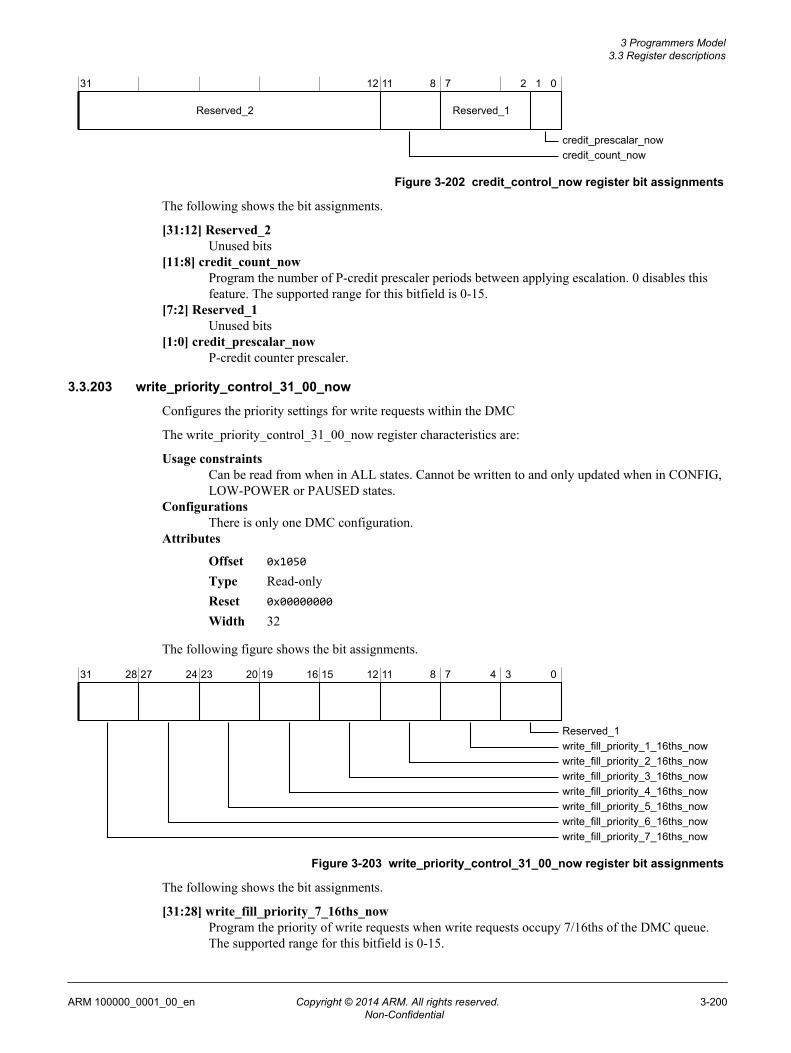
31 12 11 8 7 2 1 0
Reserved_1Reserved_2
credit_count_nowcredit_prescalar_now
Figure 3-202 credit_control_now register bit assignments
The following shows the bit assignments.
[31:12] Reserved_2Unused bits
[11:8] credit_count_nowProgram the number of P-credit prescaler periods between applying escalation. 0 disables thisfeature. The supported range for this bitfield is 0-15.
[7:2] Reserved_1Unused bits
[1:0] credit_prescalar_nowP-credit counter prescaler.
3.3.203 write_priority_control_31_00_now
Configures the priority settings for write requests within the DMC
The write_priority_control_31_00_now register characteristics are:
Usage constraintsCan be read from when in ALL states. Cannot be written to and only updated when in CONFIG,LOW-POWER or PAUSED states.
ConfigurationsThere is only one DMC configuration.
Attributes
Offset 0x1050
Type Read-onlyReset 0x00000000
Width 32
The following figure shows the bit assignments.
31 28 27 24 23 20 19 16 15 12 11 8 7 4 3 0
write_fill_priority_2_16ths_nowwrite_fill_priority_1_16ths_nowReserved_1
write_fill_priority_3_16ths_nowwrite_fill_priority_4_16ths_now
write_fill_priority_7_16ths_nowwrite_fill_priority_6_16ths_nowwrite_fill_priority_5_16ths_now
Figure 3-203 write_priority_control_31_00_now register bit assignments
The following shows the bit assignments.
[31:28] write_fill_priority_7_16ths_nowProgram the priority of write requests when write requests occupy 7/16ths of the DMC queue.The supported range for this bitfield is 0-15.
3 Programmers Model3.3 Register descriptions
ARM 100000_0001_00_en Copyright © 2014 ARM. All rights reserved. 3-200Non-Confidential

[27:24] write_fill_priority_6_16ths_nowProgram the priority of write requests when write requests occupy 6/16ths of the DMC queue.The supported range for this bitfield is 0-15.
[23:20] write_fill_priority_5_16ths_nowProgram the priority of write requests when write requests occupy 5/16ths of the DMC queue.The supported range for this bitfield is 0-15.
[19:16] write_fill_priority_4_16ths_nowProgram the priority of write requests when write requests occupy 4/16ths of the DMC queue.The supported range for this bitfield is 0-15.
[15:12] write_fill_priority_3_16ths_nowProgram the priority of write requests when write requests occupy 3/16ths of the DMC queue.The supported range for this bitfield is 0-15.
[11:8] write_fill_priority_2_16ths_nowProgram the priority of write requests when write requests occupy 2/16ths of the DMC queue.The supported range for this bitfield is 0-15.
[7:4] write_fill_priority_1_16ths_nowProgram the priority of write requests when write requests occupy 1/16th of the DMC queue.The supported range for this bitfield is 0-15.
[3:0] Reserved_1Unused bits
3.3.204 write_priority_control_63_32_now
Configures the priority settings for write requests within the DMC.
The write_priority_control_63_32_now register characteristics are:
Usage constraintsCan be read from when in ALL states. Cannot be written to and only updated when in CONFIG,LOW-POWER or PAUSED states.
ConfigurationsThere is only one DMC configuration.
Attributes
Offset 0x1054
Type Read-onlyReset 0x00000000
Width 32
The following figure shows the bit assignments.
31 28 27 24 23 20 19 16 15 12 11 8 7 4 3 0
write_fill_priority_10_16ths_nowwrite_fill_priority_9_16ths_nowwrite_fill_priority_8_16ths_now
write_fill_priority_11_16ths_nowwrite_fill_priority_12_16ths_now
write_fill_priority_15_16ths_nowwrite_fill_priority_14_16ths_nowwrite_fill_priority_13_16ths_now
Figure 3-204 write_priority_control_63_32_now register bit assignments
The following shows the bit assignments.
3 Programmers Model3.3 Register descriptions
ARM 100000_0001_00_en Copyright © 2014 ARM. All rights reserved. 3-201Non-Confidential
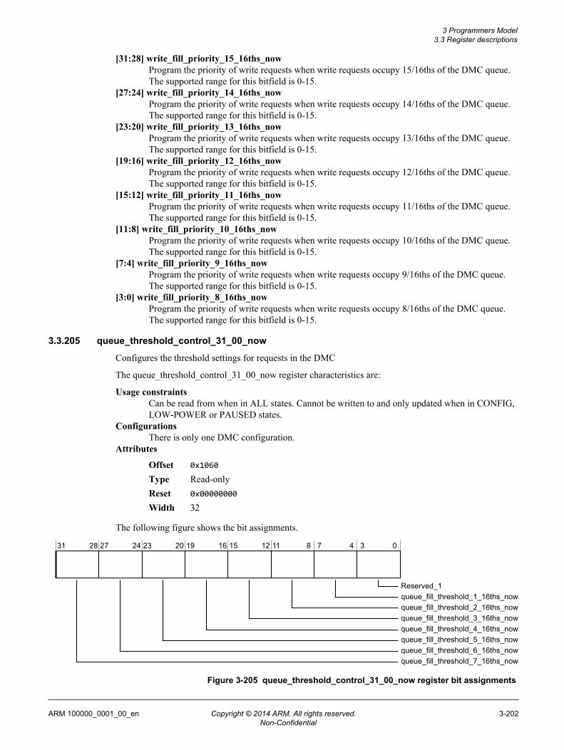
[31:28] write_fill_priority_15_16ths_nowProgram the priority of write requests when write requests occupy 15/16ths of the DMC queue.The supported range for this bitfield is 0-15.
[27:24] write_fill_priority_14_16ths_nowProgram the priority of write requests when write requests occupy 14/16ths of the DMC queue.The supported range for this bitfield is 0-15.
[23:20] write_fill_priority_13_16ths_nowProgram the priority of write requests when write requests occupy 13/16ths of the DMC queue.The supported range for this bitfield is 0-15.
[19:16] write_fill_priority_12_16ths_nowProgram the priority of write requests when write requests occupy 12/16ths of the DMC queue.The supported range for this bitfield is 0-15.
[15:12] write_fill_priority_11_16ths_nowProgram the priority of write requests when write requests occupy 11/16ths of the DMC queue.The supported range for this bitfield is 0-15.
[11:8] write_fill_priority_10_16ths_nowProgram the priority of write requests when write requests occupy 10/16ths of the DMC queue.The supported range for this bitfield is 0-15.
[7:4] write_fill_priority_9_16ths_nowProgram the priority of write requests when write requests occupy 9/16ths of the DMC queue.The supported range for this bitfield is 0-15.
[3:0] write_fill_priority_8_16ths_nowProgram the priority of write requests when write requests occupy 8/16ths of the DMC queue.The supported range for this bitfield is 0-15.
3.3.205 queue_threshold_control_31_00_now
Configures the threshold settings for requests in the DMC
The queue_threshold_control_31_00_now register characteristics are:
Usage constraintsCan be read from when in ALL states. Cannot be written to and only updated when in CONFIG,LOW-POWER or PAUSED states.
ConfigurationsThere is only one DMC configuration.
Attributes
Offset 0x1060
Type Read-onlyReset 0x00000000
Width 32
The following figure shows the bit assignments.
31 28 27 24 23 20 19 16 15 12 11 8 7 4 3 0
queue_fill_threshold_2_16ths_nowqueue_fill_threshold_1_16ths_nowReserved_1
queue_fill_threshold_3_16ths_nowqueue_fill_threshold_4_16ths_now
queue_fill_threshold_7_16ths_nowqueue_fill_threshold_6_16ths_nowqueue_fill_threshold_5_16ths_now
Figure 3-205 queue_threshold_control_31_00_now register bit assignments
3 Programmers Model3.3 Register descriptions
ARM 100000_0001_00_en Copyright © 2014 ARM. All rights reserved. 3-202Non-Confidential

The following shows the bit assignments.
[31:28] queue_fill_threshold_7_16ths_nowProgram to set the priority that requests must be equal to or above, to be accepted when thequeue is 7/16ths full. The supported range for this bitfield is 0-15.
[27:24] queue_fill_threshold_6_16ths_nowProgram to set the priority that requests must be equal to or above, to be accepted when thequeue is 6/16ths full. The supported range for this bitfield is 0-15.
[23:20] queue_fill_threshold_5_16ths_nowProgram to set the priority that requests must be equal to or above, to be accepted when thequeue is 5/16ths full. The supported range for this bitfield is 0-15.
[19:16] queue_fill_threshold_4_16ths_nowProgram to set the priority that requests must be equal to or above, to be accepted when thequeue is 4/16ths full. The supported range for this bitfield is 0-15.
[15:12] queue_fill_threshold_3_16ths_nowProgram to set the priority that requests must be equal to or above, to be accepted when thequeue is 3/16ths full. The supported range for this bitfield is 0-15.
[11:8] queue_fill_threshold_2_16ths_nowProgram to set the priority that requests must be equal to or above, to be accepted when thequeue is 2/16ths full. The supported range for this bitfield is 0-15.
[7:4] queue_fill_threshold_1_16ths_nowProgram to set the priority that requests must be equal to or above, to be accepted when thequeue is 1/16ths full. The supported range for this bitfield is 0-15.
[3:0] Reserved_1Unused bits
3.3.206 queue_threshold_control_63_32_now
Configures the threshold settings for requests in the DMC
The queue_threshold_control_63_32_now register characteristics are:
Usage constraintsCan be read from when in ALL states. Cannot be written to and only updated when in CONFIG,LOW-POWER or PAUSED states.
ConfigurationsThere is only one DMC configuration.
Attributes
Offset 0x1064
Type Read-onlyReset 0x00000000
Width 32
The following figure shows the bit assignments.
31 28 27 24 23 20 19 16 15 12 11 8 7 4 3 0
queue_fill_threshold_10_16ths_nowqueue_fill_threshold_9_16ths_nowqueue_fill_threshold_8_16ths_now
queue_fill_threshold_11_16ths_nowqueue_fill_threshold_12_16ths_now
queue_fill_threshold_15_16ths_nowqueue_fill_threshold_14_16ths_nowqueue_fill_threshold_13_16ths_now
Figure 3-206 queue_threshold_control_63_32_now register bit assignments
3 Programmers Model3.3 Register descriptions
ARM 100000_0001_00_en Copyright © 2014 ARM. All rights reserved. 3-203Non-Confidential
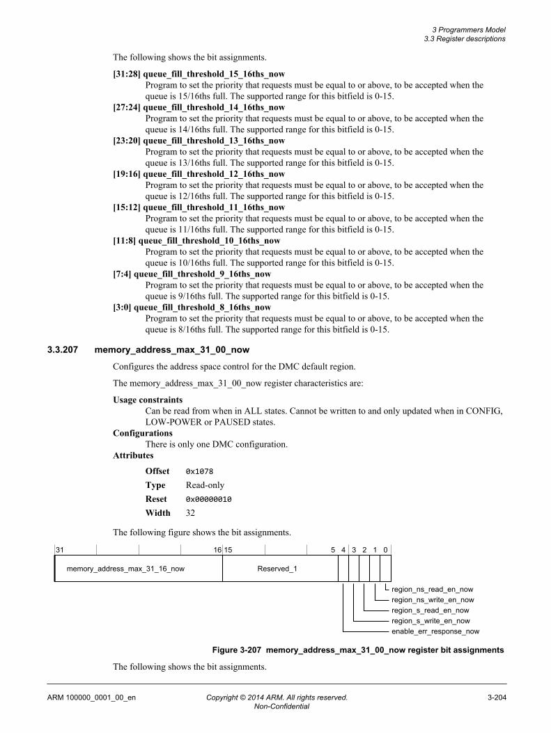
The following shows the bit assignments.
[31:28] queue_fill_threshold_15_16ths_nowProgram to set the priority that requests must be equal to or above, to be accepted when thequeue is 15/16ths full. The supported range for this bitfield is 0-15.
[27:24] queue_fill_threshold_14_16ths_nowProgram to set the priority that requests must be equal to or above, to be accepted when thequeue is 14/16ths full. The supported range for this bitfield is 0-15.
[23:20] queue_fill_threshold_13_16ths_nowProgram to set the priority that requests must be equal to or above, to be accepted when thequeue is 13/16ths full. The supported range for this bitfield is 0-15.
[19:16] queue_fill_threshold_12_16ths_nowProgram to set the priority that requests must be equal to or above, to be accepted when thequeue is 12/16ths full. The supported range for this bitfield is 0-15.
[15:12] queue_fill_threshold_11_16ths_nowProgram to set the priority that requests must be equal to or above, to be accepted when thequeue is 11/16ths full. The supported range for this bitfield is 0-15.
[11:8] queue_fill_threshold_10_16ths_nowProgram to set the priority that requests must be equal to or above, to be accepted when thequeue is 10/16ths full. The supported range for this bitfield is 0-15.
[7:4] queue_fill_threshold_9_16ths_nowProgram to set the priority that requests must be equal to or above, to be accepted when thequeue is 9/16ths full. The supported range for this bitfield is 0-15.
[3:0] queue_fill_threshold_8_16ths_nowProgram to set the priority that requests must be equal to or above, to be accepted when thequeue is 8/16ths full. The supported range for this bitfield is 0-15.
3.3.207 memory_address_max_31_00_now
Configures the address space control for the DMC default region.
The memory_address_max_31_00_now register characteristics are:
Usage constraintsCan be read from when in ALL states. Cannot be written to and only updated when in CONFIG,LOW-POWER or PAUSED states.
ConfigurationsThere is only one DMC configuration.
Attributes
Offset 0x1078
Type Read-onlyReset 0x00000010
Width 32
The following figure shows the bit assignments.
31 16 15 5 4 3 2 1 0
Reserved_1memory_address_max_31_16_now
region_s_read_en_nowregion_ns_write_en_nowregion_ns_read_en_now
region_s_write_en_nowenable_err_response_now
Figure 3-207 memory_address_max_31_00_now register bit assignments
The following shows the bit assignments.
3 Programmers Model3.3 Register descriptions
ARM 100000_0001_00_en Copyright © 2014 ARM. All rights reserved. 3-204Non-Confidential

[31:16] memory_address_max_31_16_nowProgram to set bits[31:16] of the maximum memory address.
Note
This is the address value after the address translation has been applied (if applicable).
[15:5] Reserved_1Unused bits
[4] enable_err_response_nowConfigures the response used for a request that fails address access checks.
[3] region_s_write_en_nowEnables Secure writes to the default region
[2] region_s_read_en_nowEnables Secure reads to the default region
[1] region_ns_write_en_nowEnables Non-secure writes to the default region
[0] region_ns_read_en_nowEnables Non-secure reads to the default region
3.3.208 memory_address_max_43_32_now
Configures the address space control for the DMC default region.
The memory_address_max_43_32_now register characteristics are:
Usage constraintsCan be read from when in ALL states. Cannot be written to and only updated when in CONFIG,LOW-POWER or PAUSED states.
ConfigurationsThere is only one DMC configuration.
Attributes
Offset 0x107C
Type Read-onlyReset 0x00000000
Width 32
The following figure shows the bit assignments.
31 12 11 0
Reserved_1
memory_address_max_43_32_now
Figure 3-208 memory_address_max_43_32_now register bit assignments
The following shows the bit assignments.
[31:12] Reserved_1Unused bits
[11:0] memory_address_max_43_32_nowProgram to set bits[43:32] of the maximum memory address.
Note
This is the address value after address translation has been applied (if applicable).
3 Programmers Model3.3 Register descriptions
ARM 100000_0001_00_en Copyright © 2014 ARM. All rights reserved. 3-205Non-Confidential

3.3.209 access_address_min0_31_00_now
Configures the address space control for address region 0.
The access_address_min0_31_00_now register characteristics are:
Usage constraintsCan be read from when in ALL states. Cannot be written to and only updated when in CONFIG,LOW-POWER or PAUSED states.
ConfigurationsThere is only one DMC configuration.
Attributes
Offset 0x1080
Type Read-onlyReset 0x00000000
Width 32
The following figure shows the bit assignments.
31 16 15 4 3 2 1 0
Reserved_1access_address_min0_31_16_now
region_s_read_en0_nowregion_ns_write_en0_nowregion_ns_read_en0_now
region_s_write_en0_now
Figure 3-209 access_address_min0_31_00_now register bit assignments
The following shows the bit assignments.
[31:16] access_address_min0_31_16_nowProgram to set bits[31:16] of the minimum address in the region
[15:4] Reserved_1Unused bits
[3] region_s_write_en0_nowEnables Secure writes to the region
[2] region_s_read_en0_nowEnables Secure reads to the region
[1] region_ns_write_en0_nowEnables Non-secure writes to the region
[0] region_ns_read_en0_nowEnables Non-secure reads to the region
3.3.210 access_address_min0_43_32_now
Configures the address space control for address region 0.
The access_address_min0_43_32_now register characteristics are:
Usage constraintsCan be read from when in ALL states. Cannot be written to and only updated when in CONFIG,LOW-POWER or PAUSED states.
ConfigurationsThere is only one DMC configuration.
Attributes
Offset 0x1084
Type Read-only
3 Programmers Model3.3 Register descriptions
ARM 100000_0001_00_en Copyright © 2014 ARM. All rights reserved. 3-206Non-Confidential

Reset 0x00000000
Width 32
The following figure shows the bit assignments.
31 12 11 0
Reserved_1
access_address_min0_43_32_now
Figure 3-210 access_address_min0_43_32_now register bit assignments
The following shows the bit assignments.
[31:12] Reserved_1Unused bits
[11:0] access_address_min0_43_32_nowProgram to set bits[43:32] of the minimum address in the region
3.3.211 access_address_max0_31_00_now
Configures the address space control for address region 0.
The access_address_max0_31_00_now register characteristics are:
Usage constraintsCan be read from when in ALL states. Cannot be written to and only updated when in CONFIG,LOW-POWER or PAUSED states.
ConfigurationsThere is only one DMC configuration.
Attributes
Offset 0x1088
Type Read-onlyReset 0x00000000
Width 32
The following figure shows the bit assignments.
31 16 15 0
Reserved_1access_address_max0_31_16_now
Figure 3-211 access_address_max0_31_00_now register bit assignments
The following shows the bit assignments.
[31:16] access_address_max0_31_16_nowProgram to set bits[31:16] of the maximum address in the region
[15:0] Reserved_1Unused bits
3.3.212 access_address_max0_43_32_now
Configures the address space control for address region 0.
The access_address_max0_43_32_now register characteristics are:
Usage constraintsCan be read from when in ALL states. Cannot be written to and only updated when in CONFIG,LOW-POWER or PAUSED states.
3 Programmers Model3.3 Register descriptions
ARM 100000_0001_00_en Copyright © 2014 ARM. All rights reserved. 3-207Non-Confidential

ConfigurationsThere is only one DMC configuration.
Attributes
Offset 0x108C
Type Read-onlyReset 0x00000000
Width 32
The following figure shows the bit assignments.
31 12 11 0
Reserved_1
access_address_max0_43_32_now
Figure 3-212 access_address_max0_43_32_now register bit assignments
The following shows the bit assignments.
[31:12] Reserved_1Unused bits
[11:0] access_address_max0_43_32_nowProgram to set bits[43:32] of the maximum address in the region
3.3.213 access_address_min1_31_00_now
Configures the address space control for address region 1.
The access_address_min1_31_00_now register characteristics are:
Usage constraintsCan be read from when in ALL states. Cannot be written to and only updated when in CONFIG,LOW-POWER or PAUSED states.
ConfigurationsThere is only one DMC configuration.
Attributes
Offset 0x1090
Type Read-onlyReset 0x00000000
Width 32
The following figure shows the bit assignments.
31 16 15 4 3 2 1 0
Reserved_1access_address_min1_31_16_now
region_s_read_en1_nowregion_ns_write_en1_nowregion_ns_read_en1_now
region_s_write_en1_now
Figure 3-213 access_address_min1_31_00_now register bit assignments
The following shows the bit assignments.
[31:16] access_address_min1_31_16_nowProgram to set bits[31:16] of the minimum address in the region
3 Programmers Model3.3 Register descriptions
ARM 100000_0001_00_en Copyright © 2014 ARM. All rights reserved. 3-208Non-Confidential

[15:4] Reserved_1Unused bits
[3] region_s_write_en1_nowEnables Secure writes to the region
[2] region_s_read_en1_nowEnables Secure reads to the region
[1] region_ns_write_en1_nowEnables Non-secure writes to the region
[0] region_ns_read_en1_nowEnables Non-secure reads to the region
3.3.214 access_address_min1_43_32_now
Configures the address space control for address region 1.
The access_address_min1_43_32_now register characteristics are:
Usage constraintsCan be read from when in ALL states. Cannot be written to and only updated when in CONFIG,LOW-POWER or PAUSED states.
ConfigurationsThere is only one DMC configuration.
Attributes
Offset 0x1094
Type Read-onlyReset 0x00000000
Width 32
The following figure shows the bit assignments.
31 12 11 0
Reserved_1
access_address_min1_43_32_now
Figure 3-214 access_address_min1_43_32_now register bit assignments
The following shows the bit assignments.
[31:12] Reserved_1Unused bits
[11:0] access_address_min1_43_32_nowProgram to set bits[43:32] of the minimum address in the region
3.3.215 access_address_max1_31_00_now
Configures the address space control for address region 1.
The access_address_max1_31_00_now register characteristics are:
Usage constraintsCan be read from when in ALL states. Cannot be written to and only updated when in CONFIG,LOW-POWER or PAUSED states.
ConfigurationsThere is only one DMC configuration.
Attributes
Offset 0x1098
Type Read-only
3 Programmers Model3.3 Register descriptions
ARM 100000_0001_00_en Copyright © 2014 ARM. All rights reserved. 3-209Non-Confidential

Reset 0x00000000
Width 32
The following figure shows the bit assignments.
31 16 15 0
Reserved_1access_address_max1_31_16_now
Figure 3-215 access_address_max1_31_00_now register bit assignments
The following shows the bit assignments.
[31:16] access_address_max1_31_16_nowProgram to set bits[31:16] of the maximum address in the region
[15:0] Reserved_1Unused bits
3.3.216 access_address_max1_43_32_now
Configures the address space control for address region 1.
The access_address_max1_43_32_now register characteristics are:
Usage constraintsCan be read from when in ALL states. Cannot be written to and only updated when in CONFIG,LOW-POWER or PAUSED states.
ConfigurationsThere is only one DMC configuration.
Attributes
Offset 0x109C
Type Read-onlyReset 0x00000000
Width 32
The following figure shows the bit assignments.
31 12 11 0
Reserved_1
access_address_max1_43_32_now
Figure 3-216 access_address_max1_43_32_now register bit assignments
The following shows the bit assignments.
[31:12] Reserved_1Unused bits
[11:0] access_address_max1_43_32_nowProgram to set bits[43:32] of the maximum address in the region
3.3.217 access_address_min2_31_00_now
Configures the address space control for address region 2.
The access_address_min2_31_00_now register characteristics are:
Usage constraintsCan be read from when in ALL states. Cannot be written to and only updated when in CONFIG,LOW-POWER or PAUSED states.
3 Programmers Model3.3 Register descriptions
ARM 100000_0001_00_en Copyright © 2014 ARM. All rights reserved. 3-210Non-Confidential

ConfigurationsThere is only one DMC configuration.
Attributes
Offset 0x10A0
Type Read-onlyReset 0x00000000
Width 32
The following figure shows the bit assignments.
31 16 15 4 3 2 1 0
Reserved_1access_address_min2_31_16_now
region_s_read_en2_nowregion_ns_write_en2_nowregion_ns_read_en2_now
region_s_write_en2_now
Figure 3-217 access_address_min2_31_00_now register bit assignments
The following shows the bit assignments.
[31:16] access_address_min2_31_16_nowProgram to set bits[31:16] of the minimum address in the region
[15:4] Reserved_1Unused bits
[3] region_s_write_en2_nowEnables Secure writes to the region
[2] region_s_read_en2_nowEnables Secure reads to the region
[1] region_ns_write_en2_nowEnables Non-secure writes to the region
[0] region_ns_read_en2_nowEnables Non-secure reads to the region
3.3.218 access_address_min2_43_32_now
Configures the address space control for address region 2.
The access_address_min2_43_32_now register characteristics are:
Usage constraintsCan be read from when in ALL states. Cannot be written to and only updated when in CONFIG,LOW-POWER or PAUSED states.
ConfigurationsThere is only one DMC configuration.
Attributes
Offset 0x10A4
Type Read-onlyReset 0x00000000
Width 32
The following figure shows the bit assignments.
3 Programmers Model3.3 Register descriptions
ARM 100000_0001_00_en Copyright © 2014 ARM. All rights reserved. 3-211Non-Confidential

31 12 11 0
Reserved_1
access_address_min2_43_32_now
Figure 3-218 access_address_min2_43_32_now register bit assignments
The following shows the bit assignments.
[31:12] Reserved_1Unused bits
[11:0] access_address_min2_43_32_nowProgram to set bits[43:32] of the minimum address in the region
3.3.219 access_address_max2_31_00_now
Configures the address space control for address region 2.
The access_address_max2_31_00_now register characteristics are:
Usage constraintsCan be read from when in ALL states. Cannot be written to and only updated when in CONFIG,LOW-POWER or PAUSED states.
ConfigurationsThere is only one DMC configuration.
Attributes
Offset 0x10A8
Type Read-onlyReset 0x00000000
Width 32
The following figure shows the bit assignments.
31 16 15 0
Reserved_1access_address_max2_31_16_now
Figure 3-219 access_address_max2_31_00_now register bit assignments
The following shows the bit assignments.
[31:16] access_address_max2_31_16_nowProgram to set bits[31:16] of the maximum address in the region
[15:0] Reserved_1Unused bits
3.3.220 access_address_max2_43_32_now
Configures the address space control for address region 2.
The access_address_max2_43_32_now register characteristics are:
Usage constraintsCan be read from when in ALL states. Cannot be written to and only updated when in CONFIG,LOW-POWER or PAUSED states.
ConfigurationsThere is only one DMC configuration.
Attributes
Offset 0x10AC
Type Read-only
3 Programmers Model3.3 Register descriptions
ARM 100000_0001_00_en Copyright © 2014 ARM. All rights reserved. 3-212Non-Confidential
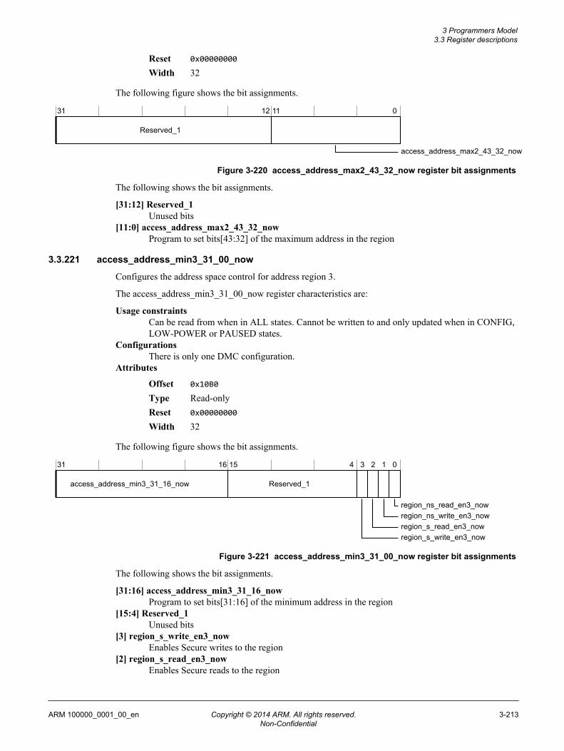
Reset 0x00000000
Width 32
The following figure shows the bit assignments.
31 12 11 0
Reserved_1
access_address_max2_43_32_now
Figure 3-220 access_address_max2_43_32_now register bit assignments
The following shows the bit assignments.
[31:12] Reserved_1Unused bits
[11:0] access_address_max2_43_32_nowProgram to set bits[43:32] of the maximum address in the region
3.3.221 access_address_min3_31_00_now
Configures the address space control for address region 3.
The access_address_min3_31_00_now register characteristics are:
Usage constraintsCan be read from when in ALL states. Cannot be written to and only updated when in CONFIG,LOW-POWER or PAUSED states.
ConfigurationsThere is only one DMC configuration.
Attributes
Offset 0x10B0
Type Read-onlyReset 0x00000000
Width 32
The following figure shows the bit assignments.
31 16 15 4 3 2 1 0
Reserved_1access_address_min3_31_16_now
region_s_read_en3_nowregion_ns_write_en3_nowregion_ns_read_en3_now
region_s_write_en3_now
Figure 3-221 access_address_min3_31_00_now register bit assignments
The following shows the bit assignments.
[31:16] access_address_min3_31_16_nowProgram to set bits[31:16] of the minimum address in the region
[15:4] Reserved_1Unused bits
[3] region_s_write_en3_nowEnables Secure writes to the region
[2] region_s_read_en3_nowEnables Secure reads to the region
3 Programmers Model3.3 Register descriptions
ARM 100000_0001_00_en Copyright © 2014 ARM. All rights reserved. 3-213Non-Confidential

[1] region_ns_write_en3_nowEnables Non-secure writes to the region
[0] region_ns_read_en3_nowEnables Non-secure reads to the region
3.3.222 access_address_min3_43_32_now
Configures the address space control for address region 3.
The access_address_min3_43_32_now register characteristics are:
Usage constraintsCan be read from when in ALL states. Cannot be written to and only updated when in CONFIG,LOW-POWER or PAUSED states.
ConfigurationsThere is only one DMC configuration.
Attributes
Offset 0x10B4
Type Read-onlyReset 0x00000000
Width 32
The following figure shows the bit assignments.
31 12 11 0
Reserved_1
access_address_min3_43_32_now
Figure 3-222 access_address_min3_43_32_now register bit assignments
The following shows the bit assignments.
[31:12] Reserved_1Unused bits
[11:0] access_address_min3_43_32_nowProgram to set bits[43:32] of the minimum address in the region
3.3.223 access_address_max3_31_00_now
Configures the address space control for address region 3.
The access_address_max3_31_00_now register characteristics are:
Usage constraintsCan be read from when in ALL states. Cannot be written to and only updated when in CONFIG,LOW-POWER or PAUSED states.
ConfigurationsThere is only one DMC configuration.
Attributes
Offset 0x10B8
Type Read-onlyReset 0x00000000
Width 32
The following figure shows the bit assignments.
3 Programmers Model3.3 Register descriptions
ARM 100000_0001_00_en Copyright © 2014 ARM. All rights reserved. 3-214Non-Confidential
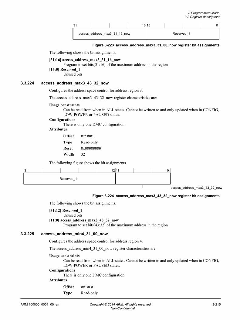
31 16 15 0
Reserved_1access_address_max3_31_16_now
Figure 3-223 access_address_max3_31_00_now register bit assignments
The following shows the bit assignments.
[31:16] access_address_max3_31_16_nowProgram to set bits[31:16] of the maximum address in the region
[15:0] Reserved_1Unused bits
3.3.224 access_address_max3_43_32_now
Configures the address space control for address region 3.
The access_address_max3_43_32_now register characteristics are:
Usage constraintsCan be read from when in ALL states. Cannot be written to and only updated when in CONFIG,LOW-POWER or PAUSED states.
ConfigurationsThere is only one DMC configuration.
Attributes
Offset 0x10BC
Type Read-onlyReset 0x00000000
Width 32
The following figure shows the bit assignments.
31 12 11 0
Reserved_1
access_address_max3_43_32_now
Figure 3-224 access_address_max3_43_32_now register bit assignments
The following shows the bit assignments.
[31:12] Reserved_1Unused bits
[11:0] access_address_max3_43_32_nowProgram to set bits[43:32] of the maximum address in the region
3.3.225 access_address_min4_31_00_now
Configures the address space control for address region 4.
The access_address_min4_31_00_now register characteristics are:
Usage constraintsCan be read from when in ALL states. Cannot be written to and only updated when in CONFIG,LOW-POWER or PAUSED states.
ConfigurationsThere is only one DMC configuration.
Attributes
Offset 0x10C0
Type Read-only
3 Programmers Model3.3 Register descriptions
ARM 100000_0001_00_en Copyright © 2014 ARM. All rights reserved. 3-215Non-Confidential

Reset 0x00000000
Width 32
The following figure shows the bit assignments.
31 16 15 4 3 2 1 0
Reserved_1access_address_min4_31_16_now
region_s_read_en4_nowregion_ns_write_en4_nowregion_ns_read_en4_now
region_s_write_en4_now
Figure 3-225 access_address_min4_31_00_now register bit assignments
The following shows the bit assignments.
[31:16] access_address_min4_31_16_nowProgram to set bits[31:16] of the minimum address in the region
[15:4] Reserved_1Unused bits
[3] region_s_write_en4_nowEnables Secure writes to the region
[2] region_s_read_en4_nowEnables Secure reads to the region
[1] region_ns_write_en4_nowEnables Non-secure writes to the region
[0] region_ns_read_en4_nowEnables Non-secure reads to the region
3.3.226 access_address_min4_43_32_now
Configures the address space control for address region 4.
The access_address_min4_43_32_now register characteristics are:
Usage constraintsCan be read from when in ALL states. Cannot be written to and only updated when in CONFIG,LOW-POWER or PAUSED states.
ConfigurationsThere is only one DMC configuration.
Attributes
Offset 0x10C4
Type Read-onlyReset 0x00000000
Width 32
The following figure shows the bit assignments.
31 12 11 0
Reserved_1
access_address_min4_43_32_now
Figure 3-226 access_address_min4_43_32_now register bit assignments
The following shows the bit assignments.
3 Programmers Model3.3 Register descriptions
ARM 100000_0001_00_en Copyright © 2014 ARM. All rights reserved. 3-216Non-Confidential

[31:12] Reserved_1Unused bits
[11:0] access_address_min4_43_32_nowProgram to set bits[43:32] of the minimum address in the region
3.3.227 access_address_max4_31_00_now
Configures the address space control for address region 4.
The access_address_max4_31_00_now register characteristics are:
Usage constraintsCan be read from when in ALL states. Cannot be written to and only updated when in CONFIG,LOW-POWER or PAUSED states.
ConfigurationsThere is only one DMC configuration.
Attributes
Offset 0x10C8
Type Read-onlyReset 0x00000000
Width 32
The following figure shows the bit assignments.
31 16 15 0
Reserved_1access_address_max4_31_16_now
Figure 3-227 access_address_max4_31_00_now register bit assignments
The following shows the bit assignments.
[31:16] access_address_max4_31_16_nowProgram to set bits[31:16] of the maximum address in the region
[15:0] Reserved_1Unused bits
3.3.228 access_address_max4_43_32_now
Configures the address space control for address region 4.
The access_address_max4_43_32_now register characteristics are:
Usage constraintsCan be read from when in ALL states. Cannot be written to and only updated when in CONFIG,LOW-POWER or PAUSED states.
ConfigurationsThere is only one DMC configuration.
Attributes
Offset 0x10CC
Type Read-onlyReset 0x00000000
Width 32
The following figure shows the bit assignments.
3 Programmers Model3.3 Register descriptions
ARM 100000_0001_00_en Copyright © 2014 ARM. All rights reserved. 3-217Non-Confidential

31 12 11 0
Reserved_1
access_address_max4_43_32_now
Figure 3-228 access_address_max4_43_32_now register bit assignments
The following shows the bit assignments.
[31:12] Reserved_1Unused bits
[11:0] access_address_max4_43_32_nowProgram to set bits[43:32] of the maximum address in the region
3.3.229 access_address_min5_31_00_now
Configures the address space control for address region 5.
The access_address_min5_31_00_now register characteristics are:
Usage constraintsCan be read from when in ALL states. Cannot be written to and only updated when in CONFIG,LOW-POWER or PAUSED states.
ConfigurationsThere is only one DMC configuration.
Attributes
Offset 0x10D0
Type Read-onlyReset 0x00000000
Width 32
The following figure shows the bit assignments.
31 16 15 4 3 2 1 0
Reserved_1access_address_min5_31_16_now
region_s_read_en5_nowregion_ns_write_en5_nowregion_ns_read_en5_now
region_s_write_en5_now
Figure 3-229 access_address_min5_31_00_now register bit assignments
The following shows the bit assignments.
[31:16] access_address_min5_31_16_nowProgram to set bits[31:16] of the minimum address in the region
[15:4] Reserved_1Unused bits
[3] region_s_write_en5_nowEnables Secure writes to the region
[2] region_s_read_en5_nowEnables Secure reads to the region
[1] region_ns_write_en5_nowEnables Non-secure writes to the region
[0] region_ns_read_en5_nowEnables Non-secure reads to the region
3 Programmers Model3.3 Register descriptions
ARM 100000_0001_00_en Copyright © 2014 ARM. All rights reserved. 3-218Non-Confidential
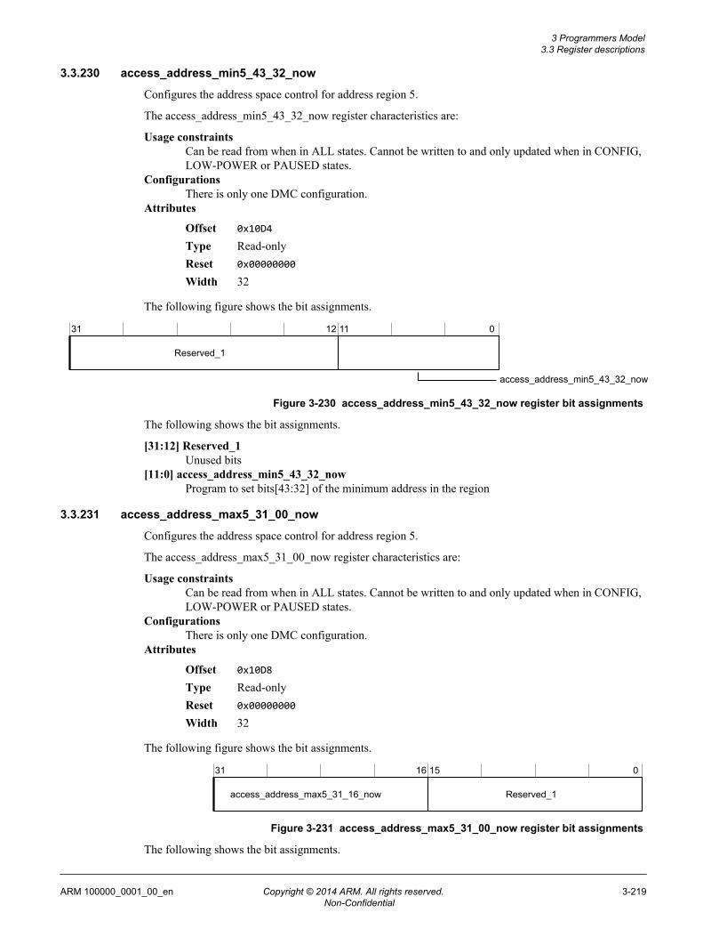
3.3.230 access_address_min5_43_32_now
Configures the address space control for address region 5.
The access_address_min5_43_32_now register characteristics are:
Usage constraintsCan be read from when in ALL states. Cannot be written to and only updated when in CONFIG,LOW-POWER or PAUSED states.
ConfigurationsThere is only one DMC configuration.
Attributes
Offset 0x10D4
Type Read-onlyReset 0x00000000
Width 32
The following figure shows the bit assignments.
31 12 11 0
Reserved_1
access_address_min5_43_32_now
Figure 3-230 access_address_min5_43_32_now register bit assignments
The following shows the bit assignments.
[31:12] Reserved_1Unused bits
[11:0] access_address_min5_43_32_nowProgram to set bits[43:32] of the minimum address in the region
3.3.231 access_address_max5_31_00_now
Configures the address space control for address region 5.
The access_address_max5_31_00_now register characteristics are:
Usage constraintsCan be read from when in ALL states. Cannot be written to and only updated when in CONFIG,LOW-POWER or PAUSED states.
ConfigurationsThere is only one DMC configuration.
Attributes
Offset 0x10D8
Type Read-onlyReset 0x00000000
Width 32
The following figure shows the bit assignments.
31 16 15 0
Reserved_1access_address_max5_31_16_now
Figure 3-231 access_address_max5_31_00_now register bit assignments
The following shows the bit assignments.
3 Programmers Model3.3 Register descriptions
ARM 100000_0001_00_en Copyright © 2014 ARM. All rights reserved. 3-219Non-Confidential

[31:16] access_address_max5_31_16_nowProgram to set bits[31:16] of the maximum address in the region
[15:0] Reserved_1Unused bits
3.3.232 access_address_max5_43_32_now
Configures the address space control for address region 5.
The access_address_max5_43_32_now register characteristics are:
Usage constraintsCan be read from when in ALL states. Cannot be written to and only updated when in CONFIG,LOW-POWER or PAUSED states.
ConfigurationsThere is only one DMC configuration.
Attributes
Offset 0x10DC
Type Read-onlyReset 0x00000000
Width 32
The following figure shows the bit assignments.
31 12 11 0
Reserved_1
access_address_max5_43_32_now
Figure 3-232 access_address_max5_43_32_now register bit assignments
The following shows the bit assignments.
[31:12] Reserved_1Unused bits
[11:0] access_address_max5_43_32_nowProgram to set bits[43:32] of the maximum address in the region
3.3.233 access_address_min6_31_00_now
Configures the address space control for address region 6.
The access_address_min6_31_00_now register characteristics are:
Usage constraintsCan be read from when in ALL states. Cannot be written to and only updated when in CONFIG,LOW-POWER or PAUSED states.
ConfigurationsThere is only one DMC configuration.
Attributes
Offset 0x10E0
Type Read-onlyReset 0x00000000
Width 32
The following figure shows the bit assignments.
3 Programmers Model3.3 Register descriptions
ARM 100000_0001_00_en Copyright © 2014 ARM. All rights reserved. 3-220Non-Confidential

31 16 15 4 3 2 1 0
Reserved_1access_address_min6_31_16_now
region_s_read_en6_nowregion_ns_write_en6_nowregion_ns_read_en6_now
region_s_write_en6_now
Figure 3-233 access_address_min6_31_00_now register bit assignments
The following shows the bit assignments.
[31:16] access_address_min6_31_16_nowProgram to set bits[31:16] of the minimum address in the region
[15:4] Reserved_1Unused bits
[3] region_s_write_en6_nowEnables Secure writes to the region
[2] region_s_read_en6_nowEnables Secure reads to the region
[1] region_ns_write_en6_nowEnables Non-secure writes to the region
[0] region_ns_read_en6_nowEnables Non-secure reads to the region
3.3.234 access_address_min6_43_32_now
Configures the address space control for address region 6.
The access_address_min6_43_32_now register characteristics are:
Usage constraintsCan be read from when in ALL states. Cannot be written to and only updated when in CONFIG,LOW-POWER or PAUSED states.
ConfigurationsThere is only one DMC configuration.
Attributes
Offset 0x10E4
Type Read-onlyReset 0x00000000
Width 32
The following figure shows the bit assignments.
31 12 11 0
Reserved_1
access_address_min6_43_32_now
Figure 3-234 access_address_min6_43_32_now register bit assignments
The following shows the bit assignments.
[31:12] Reserved_1Unused bits
[11:0] access_address_min6_43_32_nowProgram to set bits[43:32] of the minimum address in the region
3 Programmers Model3.3 Register descriptions
ARM 100000_0001_00_en Copyright © 2014 ARM. All rights reserved. 3-221Non-Confidential
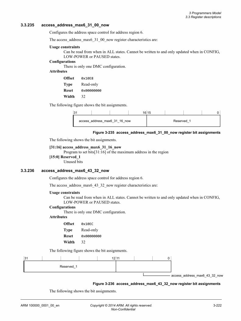
3.3.235 access_address_max6_31_00_now
Configures the address space control for address region 6.
The access_address_max6_31_00_now register characteristics are:
Usage constraintsCan be read from when in ALL states. Cannot be written to and only updated when in CONFIG,LOW-POWER or PAUSED states.
ConfigurationsThere is only one DMC configuration.
Attributes
Offset 0x10E8
Type Read-onlyReset 0x00000000
Width 32
The following figure shows the bit assignments.
31 16 15 0
Reserved_1access_address_max6_31_16_now
Figure 3-235 access_address_max6_31_00_now register bit assignments
The following shows the bit assignments.
[31:16] access_address_max6_31_16_nowProgram to set bits[31:16] of the maximum address in the region
[15:0] Reserved_1Unused bits
3.3.236 access_address_max6_43_32_now
Configures the address space control for address region 6.
The access_address_max6_43_32_now register characteristics are:
Usage constraintsCan be read from when in ALL states. Cannot be written to and only updated when in CONFIG,LOW-POWER or PAUSED states.
ConfigurationsThere is only one DMC configuration.
Attributes
Offset 0x10EC
Type Read-onlyReset 0x00000000
Width 32
The following figure shows the bit assignments.
31 12 11 0
Reserved_1
access_address_max6_43_32_now
Figure 3-236 access_address_max6_43_32_now register bit assignments
The following shows the bit assignments.
3 Programmers Model3.3 Register descriptions
ARM 100000_0001_00_en Copyright © 2014 ARM. All rights reserved. 3-222Non-Confidential

[31:12] Reserved_1Unused bits
[11:0] access_address_max6_43_32_nowProgram to set bits[43:32] of the maximum address in the region
3.3.237 access_address_min7_31_00_now
Configures the address space control for address region 7.
The access_address_min7_31_00_now register characteristics are:
Usage constraintsCan be read from when in ALL states. Cannot be written to and only updated when in CONFIG,LOW-POWER or PAUSED states.
ConfigurationsThere is only one DMC configuration.
Attributes
Offset 0x10F0
Type Read-onlyReset 0x00000000
Width 32
The following figure shows the bit assignments.
31 16 15 4 3 2 1 0
Reserved_1access_address_min7_31_16_now
region_s_read_en7_nowregion_ns_write_en7_nowregion_ns_read_en7_now
region_s_write_en7_now
Figure 3-237 access_address_min7_31_00_now register bit assignments
The following shows the bit assignments.
[31:16] access_address_min7_31_16_nowProgram to set bits[31:16] of the minimum address in the region
[15:4] Reserved_1Unused bits
[3] region_s_write_en7_nowEnables Secure writes to the region
[2] region_s_read_en7_nowEnables Secure reads to the region
[1] region_ns_write_en7_nowEnables Non-secure writes to the region
[0] region_ns_read_en7_nowEnables Non-secure reads to the region
3.3.238 access_address_min7_43_32_now
Configures the address space control for address region 7.
The access_address_min7_43_32_now register characteristics are:
Usage constraintsCan be read from when in ALL states. Cannot be written to and only updated when in CONFIG,LOW-POWER or PAUSED states.
ConfigurationsThere is only one DMC configuration.
3 Programmers Model3.3 Register descriptions
ARM 100000_0001_00_en Copyright © 2014 ARM. All rights reserved. 3-223Non-Confidential

Attributes
Offset 0x10F4
Type Read-onlyReset 0x00000000
Width 32
The following figure shows the bit assignments.
31 12 11 0
Reserved_1
access_address_min7_43_32_now
Figure 3-238 access_address_min7_43_32_now register bit assignments
The following shows the bit assignments.
[31:12] Reserved_1Unused bits
[11:0] access_address_min7_43_32_nowProgram to set bits[43:32] of the minimum address in the region
3.3.239 access_address_max7_31_00_now
Configures the address space control for address region 7.
The access_address_max7_31_00_now register characteristics are:
Usage constraintsCan be read from when in ALL states. Cannot be written to and only updated when in CONFIG,LOW-POWER or PAUSED states.
ConfigurationsThere is only one DMC configuration.
Attributes
Offset 0x10F8
Type Read-onlyReset 0x00000000
Width 32
The following figure shows the bit assignments.
31 16 15 0
Reserved_1access_address_max7_31_16_now
Figure 3-239 access_address_max7_31_00_now register bit assignments
The following shows the bit assignments.
[31:16] access_address_max7_31_16_nowProgram to set bits[31:16] of the maximum address in the region
[15:0] Reserved_1Unused bits
3.3.240 access_address_max7_43_32_now
Configures the address space control for the address region 7.
The access_address_max7_43_32_now register characteristics are:
3 Programmers Model3.3 Register descriptions
ARM 100000_0001_00_en Copyright © 2014 ARM. All rights reserved. 3-224Non-Confidential
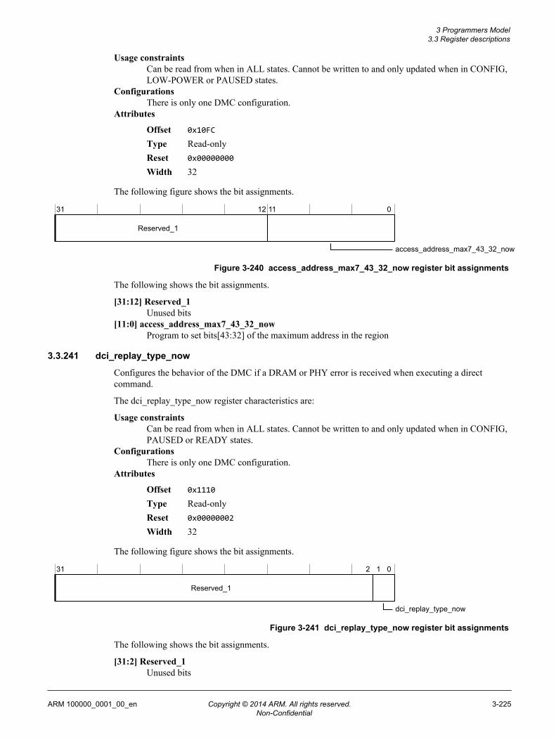
Usage constraintsCan be read from when in ALL states. Cannot be written to and only updated when in CONFIG,LOW-POWER or PAUSED states.
ConfigurationsThere is only one DMC configuration.
Attributes
Offset 0x10FC
Type Read-onlyReset 0x00000000
Width 32
The following figure shows the bit assignments.
31 12 11 0
Reserved_1
access_address_max7_43_32_now
Figure 3-240 access_address_max7_43_32_now register bit assignments
The following shows the bit assignments.
[31:12] Reserved_1Unused bits
[11:0] access_address_max7_43_32_nowProgram to set bits[43:32] of the maximum address in the region
3.3.241 dci_replay_type_now
Configures the behavior of the DMC if a DRAM or PHY error is received when executing a directcommand.
The dci_replay_type_now register characteristics are:
Usage constraintsCan be read from when in ALL states. Cannot be written to and only updated when in CONFIG,PAUSED or READY states.
ConfigurationsThere is only one DMC configuration.
Attributes
Offset 0x1110
Type Read-onlyReset 0x00000002
Width 32
The following figure shows the bit assignments.
31 2 1 0
Reserved_1
dci_replay_type_now
Figure 3-241 dci_replay_type_now register bit assignments
The following shows the bit assignments.
[31:2] Reserved_1Unused bits
3 Programmers Model3.3 Register descriptions
ARM 100000_0001_00_en Copyright © 2014 ARM. All rights reserved. 3-225Non-Confidential

[1:0] dci_replay_type_nowdci_replay_type_now bitfield.
3.3.242 refresh_control_now
Configures the type of refresh commands issued by the DMC.
The refresh_control_now register characteristics are:
Usage constraintsCan be read from when in ALL states. Cannot be written to and only updated when in CONFIGor PAUSED states.
ConfigurationsThere is only one DMC configuration.
Attributes
Offset 0x1120
Type Read-onlyReset 0x00000000
Width 32
The following figure shows the bit assignments.
31 6 5 4 3 0
Reserved_2
refresh_granularity_nowReserved_1
Figure 3-242 refresh_control_now register bit assignments
The following shows the bit assignments.
[31:6] Reserved_2Unused bits
[5:4] refresh_granularity_nowConfigures the refresh rate mode of the DMC. You must program this to match the mode of theDRAM. All DRAMs requiring refresh must use the same refresh rate.
[3:0] Reserved_1Unused bits
3.3.243 memory_type_now
Configures the DMC for the attached memory type.
The memory_type_now register characteristics are:
Usage constraintsCan be read from when in ALL states. Cannot be written to and only updated when in CONFIGor LOW-POWER states.
ConfigurationsThere is only one DMC configuration.
Attributes
Offset 0x1128
Type Read-onlyReset 0x00000101
Width 32
The following figure shows the bit assignments.
3 Programmers Model3.3 Register descriptions
ARM 100000_0001_00_en Copyright © 2014 ARM. All rights reserved. 3-226Non-Confidential

31 18 17 16 15 10 9 8 7 6 5 4 3 2 0
Reserved_4Reserved_5
Reserved_2Reserved_1memory_type_now
Reserved_3memory_device_width_nowmemory_bank_groups_now
Figure 3-243 memory_type_now register bit assignments
The following shows the bit assignments.
[31:18] Reserved_5Unused bits
[17:16] memory_bank_groups_nowProgram to configure the number of bank groups in the attached memory device
[15:10] Reserved_4Unused bits
[9:8] memory_device_width_nowProgram to configure the device widths.
[7:6] Reserved_3Unused bits
[5:4] Reserved_2Unused bits
[3] Reserved_1Unused bits
[2:0] memory_type_nowProgram to configure the attached memory type
3.3.244 scrub_control0_now
Scrub engine channel control register.
The scrub_control0_now register characteristics are:
Usage constraintsCan be read from when in ALL states. Cannot be written to and only updated when in CONFIGor LOW-POWER states.
ConfigurationsThere is only one DMC configuration.
Attributes
Offset 0x1170
Type Read-onlyReset 0x1F000000
Width 32
The following figure shows the bit assignments.
3 Programmers Model3.3 Register descriptions
ARM 100000_0001_00_en Copyright © 2014 ARM. All rights reserved. 3-227Non-Confidential

31 29 28 24 23 20 19 16 15 14 13 12 9 8 7 6 5 4 3 2 1 0
scrub_addr_mode0_nowReserved_1trigger0_now
Reserved_2completion_interrupt0_now
stop_on_page0_nowqos_for_scrub0_nowReserved_3
Reserved_5escalation_count_scrub0_nowReserved_4
outstanding_request_limit_scrub0_nowReserved_6
Figure 3-244 scrub_control0_now register bit assignments
The following shows the bit assignments.
[31:29] Reserved_6Unused bits
[28:24] outstanding_request_limit_scrub0_nowConfigures the maximum number of oustanding scrub requests for scrub program 0 Thesupported range for this bitfield is 8-31.
[23:20] Reserved_5Unused bits
[19:16] escalation_count_scrub0_nowConfigures number of escalation prescalar periods before incrementing priority for scruboperations (0 disables this feature)
[15:14] Reserved_4Unused bits
[13] stop_on_page0_nowConfigures stop_on_page of scrub operations, scrub program will pause when reach pageaddress if set
[12:9] qos_for_scrub0_nowConfigures QoS value of scrub operations
[8:7] Reserved_3Unused bits
[6] completion_interrupt0_nowConfigures whether to emit an event when the sequence completes
[5:4] Reserved_2Unused bits
[3] scrub_addr_mode0_nowConfigures scrub address mode
[2] Reserved_1Unused bits
[1:0] trigger0_nowControls the trigger event associated with the channel operation.
3.3.245 scrub_address_min0_now
Configures the address space control for the scrub engine channel.
The scrub_address_min0_now register characteristics are:
3 Programmers Model3.3 Register descriptions
ARM 100000_0001_00_en Copyright © 2014 ARM. All rights reserved. 3-228Non-Confidential

Usage constraintsCan be read from when in ALL states. Cannot be written to and only updated when in CONFIGor LOW-POWER states.
ConfigurationsThere is only one DMC configuration.
Attributes
Offset 0x1174
Type Read-onlyReset 0x00000000
Width 32
The following figure shows the bit assignments.
31 0
scrub_address_min0_now
Figure 3-245 scrub_address_min0_now register bit assignments
The following shows the bit assignments.
[31:0] scrub_address_min0_nowProgram to set the starting address for the scrub engine. When scrub_addr_mode0 is set tophysical_address this register specifies logical rank [24:22], physical bank [21:18] and physicalrow address [17:0] directly. When scrub_addr_mode0 is set to system_address this registerspecifies the address in the same address format used by incoming system transactions.
3.3.246 scrub_address_max0_now
Configures the address space control for the scrub engine channel.
The scrub_address_max0_now register characteristics are:
Usage constraintsCan be read from when in ALL states. Cannot be written to and only updated when in CONFIGor LOW-POWER states.
ConfigurationsThere is only one DMC configuration.
Attributes
Offset 0x1178
Type Read-onlyReset 0x00000000
Width 32
The following figure shows the bit assignments.
31 0
scrub_address_max0_now
Figure 3-246 scrub_address_max0_now register bit assignments
The following shows the bit assignments.
[31:0] scrub_address_max0_nowProgram to set the ending address for the scrub engine. When scrub_addr_mode0 is set tophysical_address this register specifies logical rank [24:22], physical bank [21:18] and physicalrow address [17:0] directly. When scrub_addr_mode0 is set to system_address this registerspecifies the address in the same address format used by incoming system transactions.
3 Programmers Model3.3 Register descriptions
ARM 100000_0001_00_en Copyright © 2014 ARM. All rights reserved. 3-229Non-Confidential

3.3.247 scrub_control1_now
Scrub engine channel control register.
The scrub_control1_now register characteristics are:
Usage constraintsCan be read from when in ALL states. Cannot be written to and only updated when in CONFIGor LOW-POWER states.
ConfigurationsThere is only one DMC configuration.
Attributes
Offset 0x1180
Type Read-onlyReset 0x1F000000
Width 32
The following figure shows the bit assignments.
31 29 28 24 23 20 19 16 15 14 13 12 9 8 7 6 5 4 3 2 1 0
scrub_addr_mode1_nowReserved_1trigger1_now
Reserved_2completion_interrupt1_now
stop_on_page1_nowqos_for_scrub1_nowReserved_3
Reserved_5escalation_count_scrub1_nowReserved_4
outstanding_request_limit_scrub1_nowReserved_6
Figure 3-247 scrub_control1_now register bit assignments
The following shows the bit assignments.
[31:29] Reserved_6Unused bits
[28:24] outstanding_request_limit_scrub1_nowConfigures the maximum number of oustanding scrub requests for scrub program 1 Thesupported range for this bitfield is 8-31.
[23:20] Reserved_5Unused bits
[19:16] escalation_count_scrub1_nowConfigures number of escalation prescalar periods before incrementing priority for scruboperations (0 disables this feature)
[15:14] Reserved_4Unused bits
[13] stop_on_page1_nowConfigures stop_on_page of scrub operations, scrub program will pause when reach pageaddress if set
[12:9] qos_for_scrub1_nowConfigures QoS value of scrub operations
3 Programmers Model3.3 Register descriptions
ARM 100000_0001_00_en Copyright © 2014 ARM. All rights reserved. 3-230Non-Confidential

[8:7] Reserved_3Unused bits
[6] completion_interrupt1_nowConfigures whether to emit an event when the sequence completes
[5:4] Reserved_2Unused bits
[3] scrub_addr_mode1_nowConfigures scrub address mode
[2] Reserved_1Unused bits
[1:0] trigger1_nowControls the trigger event associated with the channel operation.
3.3.248 scrub_address_min1_now
Configures the address space control for the scrub engine channel.
The scrub_address_min1_now register characteristics are:
Usage constraintsCan be read from when in ALL states. Cannot be written to and only updated when in CONFIGor LOW-POWER states.
ConfigurationsThere is only one DMC configuration.
Attributes
Offset 0x1184
Type Read-onlyReset 0x00000000
Width 32
The following figure shows the bit assignments.
31 0
scrub_address_min1_now
Figure 3-248 scrub_address_min1_now register bit assignments
The following shows the bit assignments.
[31:0] scrub_address_min1_nowProgram to set the starting address for the scrub engine. When scrub_addr_mode1 is set tophysical_address this register specifies logical rank [24:22], physical bank [21:18] and physicalrow address [17:0] directly. When scrub_addr_mode1 is set to system_address this registerspecifies the address in the same address format used by incoming system transactions.
3.3.249 scrub_address_max1_now
Configures the address space control for the scrub engine channel.
The scrub_address_max1_now register characteristics are:
Usage constraintsCan be read from when in ALL states. Cannot be written to and only updated when in CONFIGor LOW-POWER states.
ConfigurationsThere is only one DMC configuration.
Attributes
Offset 0x1188
3 Programmers Model3.3 Register descriptions
ARM 100000_0001_00_en Copyright © 2014 ARM. All rights reserved. 3-231Non-Confidential

Type Read-onlyReset 0x00000000
Width 32
The following figure shows the bit assignments.
31 0
scrub_address_max1_now
Figure 3-249 scrub_address_max1_now register bit assignments
The following shows the bit assignments.
[31:0] scrub_address_max1_nowProgram to set the ending address for the scrub engine. When scrub_addr_mode1 is set tophysical_address this register specifies logical rank [24:22], physical bank [21:18] and physicalrow address [17:0] directly. When scrub_addr_mode1 is set to system_address this registerspecifies the address in the same address format used by incoming system transactions.
3.3.250 scrub_control2_now
Scrub engine channel control register.
The scrub_control2_now register characteristics are:
Usage constraintsCan be read from when in ALL states. Cannot be written to and only updated when in CONFIGor LOW-POWER states.
ConfigurationsThere is only one DMC configuration.
Attributes
Offset 0x1190
Type Read-onlyReset 0x1F000000
Width 32
The following figure shows the bit assignments.
31 29 28 24 23 20 19 16 15 14 13 12 9 8 7 6 5 4 3 2 1 0
scrub_addr_mode2_nowReserved_1trigger2_now
Reserved_2completion_interrupt2_now
stop_on_page2_nowqos_for_scrub2_nowReserved_3
Reserved_5escalation_count_scrub2_nowReserved_4
outstanding_request_limit_scrub2_nowReserved_6
Figure 3-250 scrub_control2_now register bit assignments
The following shows the bit assignments.
3 Programmers Model3.3 Register descriptions
ARM 100000_0001_00_en Copyright © 2014 ARM. All rights reserved. 3-232Non-Confidential

[31:29] Reserved_6Unused bits
[28:24] outstanding_request_limit_scrub2_nowConfigures the maximum number of oustanding scrub requests for scrub program 2 Thesupported range for this bitfield is 8-31.
[23:20] Reserved_5Unused bits
[19:16] escalation_count_scrub2_nowConfigures number of escalation prescalar periods before incrementing priority for scruboperations (0 disables this feature)
[15:14] Reserved_4Unused bits
[13] stop_on_page2_nowConfigures stop_on_page of scrub operations, scrub program will pause when reach pageaddress if set
[12:9] qos_for_scrub2_nowConfigures QoS value of scrub operations
[8:7] Reserved_3Unused bits
[6] completion_interrupt2_nowConfigures whether to emit an event when the sequence completes
[5:4] Reserved_2Unused bits
[3] scrub_addr_mode2_nowConfigures scrub address mode
[2] Reserved_1Unused bits
[1:0] trigger2_nowControls the trigger event associated with the channel operation.
3.3.251 scrub_address_min2_now
Configures the address space control for the scrub engine channel.
The scrub_address_min2_now register characteristics are:
Usage constraintsCan be read from when in ALL states. Cannot be written to and only updated when in CONFIGor LOW-POWER states.
ConfigurationsThere is only one DMC configuration.
Attributes
Offset 0x1194
Type Read-onlyReset 0x00000000
Width 32
The following figure shows the bit assignments.
31 0
scrub_address_min2_now
Figure 3-251 scrub_address_min2_now register bit assignments
The following shows the bit assignments.
3 Programmers Model3.3 Register descriptions
ARM 100000_0001_00_en Copyright © 2014 ARM. All rights reserved. 3-233Non-Confidential
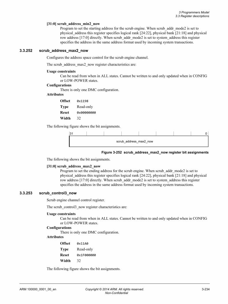
[31:0] scrub_address_min2_nowProgram to set the starting address for the scrub engine. When scrub_addr_mode2 is set tophysical_address this register specifies logical rank [24:22], physical bank [21:18] and physicalrow address [17:0] directly. When scrub_addr_mode2 is set to system_address this registerspecifies the address in the same address format used by incoming system transactions.
3.3.252 scrub_address_max2_now
Configures the address space control for the scrub engine channel.
The scrub_address_max2_now register characteristics are:
Usage constraintsCan be read from when in ALL states. Cannot be written to and only updated when in CONFIGor LOW-POWER states.
ConfigurationsThere is only one DMC configuration.
Attributes
Offset 0x1198
Type Read-onlyReset 0x00000000
Width 32
The following figure shows the bit assignments.
31 0
scrub_address_max2_now
Figure 3-252 scrub_address_max2_now register bit assignments
The following shows the bit assignments.
[31:0] scrub_address_max2_nowProgram to set the ending address for the scrub engine. When scrub_addr_mode2 is set tophysical_address this register specifies logical rank [24:22], physical bank [21:18] and physicalrow address [17:0] directly. When scrub_addr_mode2 is set to system_address this registerspecifies the address in the same address format used by incoming system transactions.
3.3.253 scrub_control3_now
Scrub engine channel control register.
The scrub_control3_now register characteristics are:
Usage constraintsCan be read from when in ALL states. Cannot be written to and only updated when in CONFIGor LOW-POWER states.
ConfigurationsThere is only one DMC configuration.
Attributes
Offset 0x11A0
Type Read-onlyReset 0x1F000000
Width 32
The following figure shows the bit assignments.
3 Programmers Model3.3 Register descriptions
ARM 100000_0001_00_en Copyright © 2014 ARM. All rights reserved. 3-234Non-Confidential

31 29 28 24 23 20 19 16 15 14 13 12 9 8 7 6 5 4 3 2 1 0
scrub_addr_mode3_nowReserved_1trigger3_now
Reserved_2completion_interrupt3_now
stop_on_page3_nowqos_for_scrub3_nowReserved_3
Reserved_5escalation_count_scrub3_nowReserved_4
outstanding_request_limit_scrub3_nowReserved_6
Figure 3-253 scrub_control3_now register bit assignments
The following shows the bit assignments.
[31:29] Reserved_6Unused bits
[28:24] outstanding_request_limit_scrub3_nowConfigures the maximum number of oustanding scrub requests for scrub program 3 Thesupported range for this bitfield is 8-31.
[23:20] Reserved_5Unused bits
[19:16] escalation_count_scrub3_nowConfigures number of escalation prescalar periods before incrementing priority for scruboperations (0 disables this feature)
[15:14] Reserved_4Unused bits
[13] stop_on_page3_nowConfigures stop_on_page of scrub operations, scrub program will pause when reach pageaddress if set
[12:9] qos_for_scrub3_nowConfigures QoS value of scrub operations
[8:7] Reserved_3Unused bits
[6] completion_interrupt3_nowConfigures whether to emit an event when the sequence completes
[5:4] Reserved_2Unused bits
[3] scrub_addr_mode3_nowConfigures scrub address mode
[2] Reserved_1Unused bits
[1:0] trigger3_nowControls the trigger event associated with the channel operation.
3.3.254 scrub_address_min3_now
Configures the address space control for the scrub engine channel.
The scrub_address_min3_now register characteristics are:
3 Programmers Model3.3 Register descriptions
ARM 100000_0001_00_en Copyright © 2014 ARM. All rights reserved. 3-235Non-Confidential

Usage constraintsCan be read from when in ALL states. Cannot be written to and only updated when in CONFIGor LOW-POWER states.
ConfigurationsThere is only one DMC configuration.
Attributes
Offset 0x11A4
Type Read-onlyReset 0x00000000
Width 32
The following figure shows the bit assignments.
31 0
scrub_address_min3_now
Figure 3-254 scrub_address_min3_now register bit assignments
The following shows the bit assignments.
[31:0] scrub_address_min3_nowProgram to set the starting address for the scrub engine. When scrub_addr_mode3 is set tophysical_address this register specifies logical rank [24:22], physical bank [21:18] and physicalrow address [17:0] directly. When scrub_addr_mode3 is set to system_address this registerspecifies the address in the same address format used by incoming system transactions.
3.3.255 scrub_address_max3_now
Configures the address space control for the scrub engine channel.
The scrub_address_max3_now register characteristics are:
Usage constraintsCan be read from when in ALL states. Cannot be written to and only updated when in CONFIGor LOW-POWER states.
ConfigurationsThere is only one DMC configuration.
Attributes
Offset 0x11A8
Type Read-onlyReset 0x00000000
Width 32
The following figure shows the bit assignments.
31 0
scrub_address_max3_now
Figure 3-255 scrub_address_max3_now register bit assignments
The following shows the bit assignments.
[31:0] scrub_address_max3_nowProgram to set the ending address for the scrub engine. When scrub_addr_mode3 is set tophysical_address this register specifies logical rank [24:22], physical bank [21:18] and physicalrow address [17:0] directly. When scrub_addr_mode3 is set to system_address this registerspecifies the address in the same address format used by incoming system transactions.
3 Programmers Model3.3 Register descriptions
ARM 100000_0001_00_en Copyright © 2014 ARM. All rights reserved. 3-236Non-Confidential

3.3.256 scrub_control4_now
Scrub engine channel control register.
The scrub_control4_now register characteristics are:
Usage constraintsCan be read from when in ALL states. Cannot be written to and only updated when in CONFIGor LOW-POWER states.
ConfigurationsThere is only one DMC configuration.
Attributes
Offset 0x11B0
Type Read-onlyReset 0x1F000000
Width 32
The following figure shows the bit assignments.
31 29 28 24 23 20 19 16 15 14 13 12 9 8 7 6 5 4 3 2 1 0
scrub_addr_mode4_nowReserved_1trigger4_now
Reserved_2completion_interrupt4_now
stop_on_page4_nowqos_for_scrub4_nowReserved_3
Reserved_5escalation_count_scrub4_nowReserved_4
outstanding_request_limit_scrub4_nowReserved_6
Figure 3-256 scrub_control4_now register bit assignments
The following shows the bit assignments.
[31:29] Reserved_6Unused bits
[28:24] outstanding_request_limit_scrub4_nowConfigures the maximum number of oustanding scrub requests for scrub program 4 Thesupported range for this bitfield is 8-31.
[23:20] Reserved_5Unused bits
[19:16] escalation_count_scrub4_nowConfigures number of escalation prescalar periods before incrementing priority for scruboperations (0 disables this feature)
[15:14] Reserved_4Unused bits
[13] stop_on_page4_nowConfigures stop_on_page of scrub operations, scrub program will pause when reach pageaddress if set
[12:9] qos_for_scrub4_nowConfigures QoS value of scrub operations
3 Programmers Model3.3 Register descriptions
ARM 100000_0001_00_en Copyright © 2014 ARM. All rights reserved. 3-237Non-Confidential

[8:7] Reserved_3Unused bits
[6] completion_interrupt4_nowConfigures whether to emit an event when the sequence completes
[5:4] Reserved_2Unused bits
[3] scrub_addr_mode4_nowConfigures scrub address mode
[2] Reserved_1Unused bits
[1:0] trigger4_nowControls the trigger event associated with the channel operation.
3.3.257 scrub_address_min4_now
Configures the address space control for the scrub engine channel.
The scrub_address_min4_now register characteristics are:
Usage constraintsCan be read from when in ALL states. Cannot be written to and only updated when in CONFIGor LOW-POWER states.
ConfigurationsThere is only one DMC configuration.
Attributes
Offset 0x11B4
Type Read-onlyReset 0x00000000
Width 32
The following figure shows the bit assignments.
31 0
scrub_address_min4_now
Figure 3-257 scrub_address_min4_now register bit assignments
The following shows the bit assignments.
[31:0] scrub_address_min4_nowProgram to set the starting address for the scrub engine. When scrub_addr_mode4 is set tophysical_address this register specifies logical rank [24:22], physical bank [21:18] and physicalrow address [17:0] directly. When scrub_addr_mode4 is set to system_address this registerspecifies the address in the same address format used by incoming system transactions.
3.3.258 scrub_address_max4_now
Configures the address space control for the scrub engine channel.
The scrub_address_max4_now register characteristics are:
Usage constraintsCan be read from when in ALL states. Cannot be written to and only updated when in CONFIGor LOW-POWER states.
ConfigurationsThere is only one DMC configuration.
Attributes
Offset 0x11B8
3 Programmers Model3.3 Register descriptions
ARM 100000_0001_00_en Copyright © 2014 ARM. All rights reserved. 3-238Non-Confidential
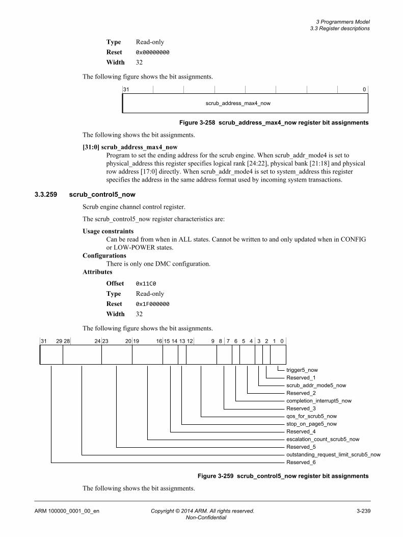
Type Read-onlyReset 0x00000000
Width 32
The following figure shows the bit assignments.
31 0
scrub_address_max4_now
Figure 3-258 scrub_address_max4_now register bit assignments
The following shows the bit assignments.
[31:0] scrub_address_max4_nowProgram to set the ending address for the scrub engine. When scrub_addr_mode4 is set tophysical_address this register specifies logical rank [24:22], physical bank [21:18] and physicalrow address [17:0] directly. When scrub_addr_mode4 is set to system_address this registerspecifies the address in the same address format used by incoming system transactions.
3.3.259 scrub_control5_now
Scrub engine channel control register.
The scrub_control5_now register characteristics are:
Usage constraintsCan be read from when in ALL states. Cannot be written to and only updated when in CONFIGor LOW-POWER states.
ConfigurationsThere is only one DMC configuration.
Attributes
Offset 0x11C0
Type Read-onlyReset 0x1F000000
Width 32
The following figure shows the bit assignments.
31 29 28 24 23 20 19 16 15 14 13 12 9 8 7 6 5 4 3 2 1 0
scrub_addr_mode5_nowReserved_1trigger5_now
Reserved_2completion_interrupt5_now
stop_on_page5_nowqos_for_scrub5_nowReserved_3
Reserved_5escalation_count_scrub5_nowReserved_4
outstanding_request_limit_scrub5_nowReserved_6
Figure 3-259 scrub_control5_now register bit assignments
The following shows the bit assignments.
3 Programmers Model3.3 Register descriptions
ARM 100000_0001_00_en Copyright © 2014 ARM. All rights reserved. 3-239Non-Confidential

[31:29] Reserved_6Unused bits
[28:24] outstanding_request_limit_scrub5_nowConfigures the maximum number of oustanding scrub requests for scrub program 5 Thesupported range for this bitfield is 8-31.
[23:20] Reserved_5Unused bits
[19:16] escalation_count_scrub5_nowConfigures number of escalation prescalar periods before incrementing priority for scruboperations (0 disables this feature)
[15:14] Reserved_4Unused bits
[13] stop_on_page5_nowConfigures stop_on_page of scrub operations, scrub program will pause when reach pageaddress if set
[12:9] qos_for_scrub5_nowConfigures QoS value of scrub operations
[8:7] Reserved_3Unused bits
[6] completion_interrupt5_nowConfigures whether to emit an event when the sequence completes
[5:4] Reserved_2Unused bits
[3] scrub_addr_mode5_nowConfigures scrub address mode
[2] Reserved_1Unused bits
[1:0] trigger5_nowControls the trigger event associated with the channel operation.
3.3.260 scrub_address_min5_now
Configures the address space control for the scrub engine channel.
The scrub_address_min5_now register characteristics are:
Usage constraintsCan be read from when in ALL states. Cannot be written to and only updated when in CONFIGor LOW-POWER states.
ConfigurationsThere is only one DMC configuration.
Attributes
Offset 0x11C4
Type Read-onlyReset 0x00000000
Width 32
The following figure shows the bit assignments.
31 0
scrub_address_min5_now
Figure 3-260 scrub_address_min5_now register bit assignments
The following shows the bit assignments.
3 Programmers Model3.3 Register descriptions
ARM 100000_0001_00_en Copyright © 2014 ARM. All rights reserved. 3-240Non-Confidential

[31:0] scrub_address_min5_nowProgram to set the starting address for the scrub engine. When scrub_addr_mode5 is set tophysical_address this register specifies logical rank [24:22], physical bank [21:18] and physicalrow address [17:0] directly. When scrub_addr_mode5 is set to system_address this registerspecifies the address in the same address format used by incoming system transactions.
3.3.261 scrub_address_max5_now
Configures the address space control for the scrub engine channel.
The scrub_address_max5_now register characteristics are:
Usage constraintsCan be read from when in ALL states. Cannot be written to and only updated when in CONFIGor LOW-POWER states.
ConfigurationsThere is only one DMC configuration.
Attributes
Offset 0x11C8
Type Read-onlyReset 0x00000000
Width 32
The following figure shows the bit assignments.
31 0
scrub_address_max5_now
Figure 3-261 scrub_address_max5_now register bit assignments
The following shows the bit assignments.
[31:0] scrub_address_max5_nowProgram to set the ending address for the scrub engine. When scrub_addr_mode5 is set tophysical_address this register specifies logical rank [24:22], physical bank [21:18] and physicalrow address [17:0] directly. When scrub_addr_mode5 is set to system_address this registerspecifies the address in the same address format used by incoming system transactions.
3.3.262 scrub_control6_now
Scrub engine channel control register.
The scrub_control6_now register characteristics are:
Usage constraintsCan be read from when in ALL states. Cannot be written to and only updated when in CONFIGor LOW-POWER states.
ConfigurationsThere is only one DMC configuration.
Attributes
Offset 0x11D0
Type Read-onlyReset 0x1F000000
Width 32
The following figure shows the bit assignments.
3 Programmers Model3.3 Register descriptions
ARM 100000_0001_00_en Copyright © 2014 ARM. All rights reserved. 3-241Non-Confidential

31 29 28 24 23 20 19 16 15 14 13 12 9 8 7 6 5 4 3 2 1 0
scrub_addr_mode6_nowReserved_1trigger6_now
Reserved_2completion_interrupt6_now
stop_on_page6_nowqos_for_scrub6_nowReserved_3
Reserved_5escalation_count_scrub6_nowReserved_4
outstanding_request_limit_scrub6_nowReserved_6
Figure 3-262 scrub_control6_now register bit assignments
The following shows the bit assignments.
[31:29] Reserved_6Unused bits
[28:24] outstanding_request_limit_scrub6_nowConfigures the maximum number of oustanding scrub requests for scrub program 6 Thesupported range for this bitfield is 8-31.
[23:20] Reserved_5Unused bits
[19:16] escalation_count_scrub6_nowConfigures number of escalation prescalar periods before incrementing priority for scruboperations (0 disables this feature)
[15:14] Reserved_4Unused bits
[13] stop_on_page6_nowConfigures stop_on_page of scrub operations, scrub program will pause when reach pageaddress if set
[12:9] qos_for_scrub6_nowConfigures QoS value of scrub operations
[8:7] Reserved_3Unused bits
[6] completion_interrupt6_nowConfigures whether to emit an event when the sequence completes
[5:4] Reserved_2Unused bits
[3] scrub_addr_mode6_nowConfigures scrub address mode
[2] Reserved_1Unused bits
[1:0] trigger6_nowControls the trigger event associated with the channel operation.
3.3.263 scrub_address_min6_now
Configures the address space control for the scrub engine channel.
The scrub_address_min6_now register characteristics are:
3 Programmers Model3.3 Register descriptions
ARM 100000_0001_00_en Copyright © 2014 ARM. All rights reserved. 3-242Non-Confidential

Usage constraintsCan be read from when in ALL states. Cannot be written to and only updated when in CONFIGor LOW-POWER states.
ConfigurationsThere is only one DMC configuration.
Attributes
Offset 0x11D4
Type Read-onlyReset 0x00000000
Width 32
The following figure shows the bit assignments.
31 0
scrub_address_min6_now
Figure 3-263 scrub_address_min6_now register bit assignments
The following shows the bit assignments.
[31:0] scrub_address_min6_nowProgram to set the starting address for the scrub engine. When scrub_addr_mode6 is set tophysical_address this register specifies logical rank [24:22], physical bank [21:18] and physicalrow address [17:0] directly. When scrub_addr_mode6 is set to system_address this registerspecifies the address in the same address format used by incoming system transactions.
3.3.264 scrub_address_max6_now
Configures the address space control for the scrub engine channel.
The scrub_address_max6_now register characteristics are:
Usage constraintsCan be read from when in ALL states. Cannot be written to and only updated when in CONFIGor LOW-POWER states.
ConfigurationsThere is only one DMC configuration.
Attributes
Offset 0x11D8
Type Read-onlyReset 0x00000000
Width 32
The following figure shows the bit assignments.
31 0
scrub_address_max6_now
Figure 3-264 scrub_address_max6_now register bit assignments
The following shows the bit assignments.
[31:0] scrub_address_max6_nowProgram to set the ending address for the scrub engine. When scrub_addr_mode6 is set tophysical_address this register specifies logical rank [24:22], physical bank [21:18] and physicalrow address [17:0] directly. When scrub_addr_mode6 is set to system_address this registerspecifies the address in the same address format used by incoming system transactions.
3 Programmers Model3.3 Register descriptions
ARM 100000_0001_00_en Copyright © 2014 ARM. All rights reserved. 3-243Non-Confidential

3.3.265 scrub_control7_now
Scrub engine channel control register.
The scrub_control7_now register characteristics are:
Usage constraintsCan be read from when in ALL states. Cannot be written to and only updated when in CONFIGor LOW-POWER states.
ConfigurationsThere is only one DMC configuration.
Attributes
Offset 0x11E0
Type Read-onlyReset 0x1F000000
Width 32
The following figure shows the bit assignments.
31 29 28 24 23 20 19 16 15 14 13 12 9 8 7 6 5 4 3 2 1 0
scrub_addr_mode7_nowReserved_1trigger7_now
Reserved_2completion_interrupt7_now
stop_on_page7_nowqos_for_scrub7_nowReserved_3
Reserved_5escalation_count_scrub7_nowReserved_4
outstanding_request_limit_scrub7_nowReserved_6
Figure 3-265 scrub_control7_now register bit assignments
The following shows the bit assignments.
[31:29] Reserved_6Unused bits
[28:24] outstanding_request_limit_scrub7_nowConfigures the maximum number of oustanding scrub requests for scrub program 7 Thesupported range for this bitfield is 8-31.
[23:20] Reserved_5Unused bits
[19:16] escalation_count_scrub7_nowConfigures number of escalation prescalar periods before incrementing priority for scruboperations (0 disables this feature)
[15:14] Reserved_4Unused bits
[13] stop_on_page7_nowConfigures stop_on_page of scrub operations, scrub program will pause when reach pageaddress if set
[12:9] qos_for_scrub7_nowConfigures QoS value of scrub operations
3 Programmers Model3.3 Register descriptions
ARM 100000_0001_00_en Copyright © 2014 ARM. All rights reserved. 3-244Non-Confidential

[8:7] Reserved_3Unused bits
[6] completion_interrupt7_nowConfigures whether to emit an event when the sequence completes
[5:4] Reserved_2Unused bits
[3] scrub_addr_mode7_nowConfigures scrub address mode
[2] Reserved_1Unused bits
[1:0] trigger7_nowControls the trigger event associated with the channel operation.
3.3.266 scrub_address_min7_now
Configures the address space control for the scrub engine channel.
The scrub_address_min7_now register characteristics are:
Usage constraintsCan be read from when in ALL states. Cannot be written to and only updated when in CONFIGor LOW-POWER states.
ConfigurationsThere is only one DMC configuration.
Attributes
Offset 0x11E4
Type Read-onlyReset 0x00000000
Width 32
The following figure shows the bit assignments.
31 0
scrub_address_min7_now
Figure 3-266 scrub_address_min7_now register bit assignments
The following shows the bit assignments.
[31:0] scrub_address_min7_nowProgram to set the starting address for the scrub engine. When scrub_addr_mode7 is set tophysical_address this register specifies logical rank [24:22], physical bank [21:18] and physicalrow address [17:0] directly. When scrub_addr_mode7 is set to system_address this registerspecifies the address in the same address format used by incoming system transactions.
3.3.267 scrub_address_max7_now
Configures the address space control for the scrub engine channel.
The scrub_address_max7_now register characteristics are:
Usage constraintsCan be read from when in ALL states. Cannot be written to and only updated when in CONFIGor LOW-POWER states.
ConfigurationsThere is only one DMC configuration.
Attributes
Offset 0x11E8
3 Programmers Model3.3 Register descriptions
ARM 100000_0001_00_en Copyright © 2014 ARM. All rights reserved. 3-245Non-Confidential

Type Read-onlyReset 0x00000000
Width 32
The following figure shows the bit assignments.
31 0
scrub_address_max7_now
Figure 3-267 scrub_address_max7_now register bit assignments
The following shows the bit assignments.
[31:0] scrub_address_max7_nowProgram to set the ending address for the scrub engine. When scrub_addr_mode7 is set tophysical_address this register specifies logical rank [24:22], physical bank [21:18] and physicalrow address [17:0] directly. When scrub_addr_mode7 is set to system_address this registerspecifies the address in the same address format used by incoming system transactions.
3.3.268 feature_control_now
Control register for DMC features.
The feature_control_now register characteristics are:
Usage constraintsCan be read from when in ALL states. Cannot be written to and only updated when in CONFIG,LOW-POWER or PAUSED states.
ConfigurationsThere is only one DMC configuration.
Attributes
Offset 0x11F0
Type Read-onlyReset 0x0AA00000
Width 32
The following figure shows the bit assignments.
3 Programmers Model3.3 Register descriptions
ARM 100000_0001_00_en Copyright © 2014 ARM. All rights reserved. 3-246Non-Confidential

31 29 28 27 20 19 18 17 16 15 14 13 12 9 8 7 4 3 2 1 0
Reserved_1crc_enable_nowwrite_dbi_enable_now
two_t_timing_nowzqcs_after_n_ref_now
temp_poll_after_xsref_nowtemp_poll_after_n_ref_nowzqcs_after_xsref_now
address_mirroring_nowtrr_enable_nowReserved_2
mrs_output_inversion_nowlvl_wakeup_en_now
alert_mode_nowaddress_mirroring_mask_nowdfi_err_mode_now
Reserved_3
Figure 3-268 feature_control_now register bit assignments
The following shows the bit assignments.
[31:29] Reserved_3Unused bits
[28] alert_mode_nowConfigures the DMC behavior in response to dfi_alert_n being asserted.
Note
When performing DIMM CA training using the ALERT pin this mode must be set to interrupt-only mode.
[27:20] address_mirroring_mask_nowEach bit determines if address mirroring as per the DDR3/DDR4 RDIMM Design Specificationmust be applied to the corresponding rank. Set to 1 to enable mirroring, 0 to disable. Normally,this bit must be set high for odd physical ranks.
[19] dfi_err_mode_nowConfigures the DMC behavior in response to dfi_err being asserted.
[18] lvl_wakeup_en_nowProgram to enable the DMC to bring a rank out of self-refresh to perform PHY training. Thismust not be enabled when using geardown mode.
[17] mrs_output_inversion_nowProgram to enable output inversion for MRS commands for DDR4 DIMMs.
[16] address_mirroring_nowProgram to enable address mirroring for ranks identified by address_mirroring_mask.
[15] trr_enable_nowProgram to enable issue of Target Row Refresh command on detection of potential maximumactivate count (tMAC) violation. Must only be enabled for memories supporting this command.
[14] Reserved_2Unused bits
[13] temp_poll_after_xsref_nowProgram to insert an automatic temperature status poll command following exit from self-refresh.
[12:9] temp_poll_after_n_ref_nowProgram to insert an automatic temperature status poll command following issue of nAUTOREFRESH commands. 0 disables the functionality. 1 is RESERVED
3 Programmers Model3.3 Register descriptions
ARM 100000_0001_00_en Copyright © 2014 ARM. All rights reserved. 3-247Non-Confidential

[8] zqcs_after_xsref_nowProgram to insert an automatic ZQC short calibration command following exit from self-refresh.
[7:4] zqcs_after_n_ref_nowProgram to insert an automatic ZQC short calibration command following n refreshes. 0 -disables the functionality. 1 is RESERVED
[3] two_t_timing_nowProgram to enable or disable 2T command timing.
[2] Reserved_1Unused bits
[1] crc_enable_nowProgram to enable or disable Cyclic Redundancy Check (CRC) functionality on write data.
Note
When you enable CRC, the parameters t_wr, t_wtr and t_wtw must be extended by one cycle toaccommodate the CRC functionality.
[0] write_dbi_enable_nowProgram to enable or disable Data Bus Inversion (DBI) functionality for writes.
3.3.269 mux_control_now
Control muxing options for the DMC.
The mux_control_now register characteristics are:
Usage constraintsCan be read from when in ALL states. Cannot be written to and only updated when in CONFIG,LOW-POWER or PAUSED states.
ConfigurationsThere is only one DMC configuration.
Attributes
Offset 0x11F4
Type Read-onlyReset 0x00000000
Width 32
The following figure shows the bit assignments.
31 11 10 8 7 6 5 4 3 2 1 0
Reserved_1
ck_mux_control_nowcke_mux_control_nowcs_mux_control_now
rst_mux_control_nowcid_mask_now
Figure 3-269 mux_control_now register bit assignments
The following shows the bit assignments.
[31:11] Reserved_1Unused bits
[10:8] cid_mask_nowProgram to mask inclusion of dfi_cid[2:0] output in parity calculation, where for each bit ofcid_mask[2:0] a value of 1 means include the corresponding bit of dfi_cid[2:0].
[7:6] rst_mux_control_nowProgram to control muxing of dfi_reset_n output for DIMM applications.
3 Programmers Model3.3 Register descriptions
ARM 100000_0001_00_en Copyright © 2014 ARM. All rights reserved. 3-248Non-Confidential

[5:4] ck_mux_control_nowProgram to control muxing of dfi_ck output for DIMM applications.
[3:2] cke_mux_control_nowProgram to control muxing of dfi_cke output for DIMM applications.
[1:0] cs_mux_control_nowProgram to control muxing of dfi_cs_n output for DIMM applications.
3.3.270 rank_remap_control_now
Control register for rank remap.
The rank_remap_control_now register characteristics are:
Usage constraintsCan be read from when in ALL states. Cannot be written to and only updated when in CONFIG,LOW-POWER or PAUSED states.
ConfigurationsThere is only one DMC configuration.
Attributes
Offset 0x11F8
Type Read-onlyReset 0x76543210
Width 32
The following figure shows the bit assignments.
31 30 28 27 26 24 23 22 20 19 18 16 15 14 12 11 10 8 7 6 4 3 2 0
rank_remap_cs1_nowrank_mask_cs0_nowrank_remap_cs0_now
rank_mask_cs1_nowrank_remap_cs2_now
rank_mask_cs3_nowrank_remap_cs3_nowrank_mask_cs2_now
rank_remap_cs5_nowrank_mask_cs4_nowrank_remap_cs4_now
rank_mask_cs5_nowrank_remap_cs6_now
rank_mask_cs7_nowrank_remap_cs7_nowrank_mask_cs6_now
Figure 3-270 rank_remap_control_now register bit assignments
The following shows the bit assignments.
[31] rank_mask_cs7_nowProgram to cause the DMC to abort all transactions to DRAM rank 7. Can be used to blocktransactions to a rank that is in maximum power down.
[30:28] rank_remap_cs7_nowProgram to remap rank address 7 to DRAM rank 0..7. Used to remap ranks when replacingDIMMs.
[27] rank_mask_cs6_nowProgram to cause the DMC to abort all transactions to DRAM rank 6. Can be used to blocktransactions to a rank that is in maximum power down.
3 Programmers Model3.3 Register descriptions
ARM 100000_0001_00_en Copyright © 2014 ARM. All rights reserved. 3-249Non-Confidential

[26:24] rank_remap_cs6_nowProgram to remap rank address 6 to DRAM rank 0..7. Used to remap ranks when replacingDIMMs.
[23] rank_mask_cs5_nowProgram to cause the DMC to abort all transactions to DRAM rank 5. Can be used to blocktransactions to a rank that is in maximum power down.
[22:20] rank_remap_cs5_nowProgram to remap rank address 5 to DRAM rank 0..7. Used to remap ranks when replacingDIMMs.
[19] rank_mask_cs4_nowProgram to cause the DMC to abort all transactions to DRAM rank 4. Can be used to blocktransactions to a rank that is in maximum power down.
[18:16] rank_remap_cs4_nowProgram to remap rank address 4 to DRAM rank 0..7. Used to remap ranks when replacingDIMMs.
[15] rank_mask_cs3_nowProgram to cause the DMC to abort all transactions to DRAM rank 3. Can be used to blocktransactions to a rank that is in maximum power down.
[14:12] rank_remap_cs3_nowProgram to remap rank address 3 to DRAM rank 0..7. Used to remap ranks when replacingDIMMs.
[11] rank_mask_cs2_nowProgram to cause the DMC to abort all transactions to DRAM rank 2. Can be used to blocktransactions to a rank that is in maximum power down.
[10:8] rank_remap_cs2_nowProgram to remap rank address 2 to DRAM rank 0..7. Used to remap ranks when replacingDIMMs.
[7] rank_mask_cs1_nowProgram to cause the DMC to abort all transactions to DRAM rank 1. Can be used to blocktransactions to a rank that is in maximum power down.
[6:4] rank_remap_cs1_nowProgram to remap rank address 1 to DRAM rank 0..7. Used to remap ranks when replacingDIMMs.
[3] rank_mask_cs0_nowProgram to cause the DMC to abort all transactions to DRAM rank 0. Can be used to blocktransactions to a rank that is in maximum power down.
[2:0] rank_remap_cs0_nowProgram to remap rank address 0 to DRAM rank 0..7. Used to remap ranks when replacingDIMMs.
3.3.271 scrub_control_now
Scrub engine channel control register.
The scrub_control_now register characteristics are:
Usage constraintsCan be read from when in ALL states. Cannot be written to and only updated when in CONFIGor LOW-POWER states.
ConfigurationsThere is only one DMC configuration.
Attributes
Offset 0x11FC
Type Read-onlyReset 0x00001F00
Width 32
3 Programmers Model3.3 Register descriptions
ARM 100000_0001_00_en Copyright © 2014 ARM. All rights reserved. 3-250Non-Confidential

The following figure shows the bit assignments.
31 15 14 8 7 3 2 0
Reserved_1Reserved_2
outstanding_scrub_request_limit_nowescalation_prescalar_scrub_now
Figure 3-271 scrub_control_now register bit assignments
The following shows the bit assignments.
[31:15] Reserved_2Unused bits
[14:8] outstanding_scrub_request_limit_nowConfigures the maximum number of oustanding scrub requests across all scrub programs Thesupported range for this bitfield is 1-127.
[7:3] Reserved_1Unused bits
[2:0] escalation_prescalar_scrub_nowConfigures escalation prescalar period for use across all scrub programs
3.3.272 t_refi_now
Configures the refresh interval timing parameter. It must be programmed to the device average all-bankAUTOREFRESH interval, divided by 8.
The t_refi_now register characteristics are:
Usage constraintsCan be read from when in ALL states. Cannot be written to and only updated when in CONFIG,LOW-POWER or PAUSED states.
ConfigurationsThere is only one DMC configuration.
Attributes
Offset 0x1200
Type Read-onlyReset 0x00090100
Width 32
The following figure shows the bit assignments.
31 21 20 16 15 11 10 0
t_refi_nowReserved_1Reserved_2Reserved_3
Figure 3-272 t_refi_now register bit assignments
The following shows the bit assignments.
[31:21] Reserved_3Unused bits
[20:16] Reserved_2Unused bits
[15:11] Reserved_1Unused bits
[10:0] t_refi_nowt_refi_now bitfield. The supported range for this bitfield is 63-2047.
3 Programmers Model3.3 Register descriptions
ARM 100000_0001_00_en Copyright © 2014 ARM. All rights reserved. 3-251Non-Confidential
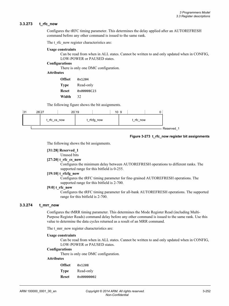
3.3.273 t_rfc_now
Configures the tRFC timing parameter. This determines the delay applied after an AUTOREFRESHcommand before any other command is issued to the same rank.
The t_rfc_now register characteristics are:
Usage constraintsCan be read from when in ALL states. Cannot be written to and only updated when in CONFIG,LOW-POWER or PAUSED states.
ConfigurationsThere is only one DMC configuration.
Attributes
Offset 0x1204
Type Read-onlyReset 0x00008C23
Width 32
The following figure shows the bit assignments.
31 28 27 20 19 10 9 0
t_rfc_nowt_rfcfg_nowt_rfc_cs_now
Reserved_1
Figure 3-273 t_rfc_now register bit assignments
The following shows the bit assignments.
[31:28] Reserved_1Unused bits
[27:20] t_rfc_cs_nowConfigures the minimum delay between AUTOREFRESH operations to different ranks. Thesupported range for this bitfield is 0-255.
[19:10] t_rfcfg_nowConfigures the tRFC timing parameter for fine-grained AUTOREFRESH operations. Thesupported range for this bitfield is 2-700.
[9:0] t_rfc_nowConfigures the tRFC timing parameter for all-bank AUTOREFRESH operations. The supportedrange for this bitfield is 2-700.
3.3.274 t_mrr_now
Configures the tMRR timing parameter. This determines the Mode Register Read (including Multi-Purpose Register Reads) command delay before any other command is issued to the same rank. Use thisvalue to determine the data cycles returned as a result of an MRR command.
The t_mrr_now register characteristics are:
Usage constraintsCan be read from when in ALL states. Cannot be written to and only updated when in CONFIG,LOW-POWER or PAUSED states.
ConfigurationsThere is only one DMC configuration.
Attributes
Offset 0x1208
Type Read-onlyReset 0x00000002
3 Programmers Model3.3 Register descriptions
ARM 100000_0001_00_en Copyright © 2014 ARM. All rights reserved. 3-252Non-Confidential

Width 32
The following figure shows the bit assignments.
31 9 8 7 6 0
t_mrr_nowReserved_2
Reserved_1
Figure 3-274 t_mrr_now register bit assignments
The following shows the bit assignments.
[31:9] Reserved_2Unused bits
[8:7] Reserved_1Unused bits
[6:0] t_mrr_nowt_mrr_now bitfield. The supported range for this bitfield is 1-127.
3.3.275 t_mrw_now
Configures the tMRW timing parameter. This determines the delay applied after a Mode Register Write(including Multi-Purpose Register Writes) command before any other command is issued to the samerank. Use this value for all delays associated with mode register write and set commands, so the largestof these delays must be programmed.
The t_mrw_now register characteristics are:
Usage constraintsCan be read from when in ALL states. Cannot be written to and only updated when in CONFIG,LOW-POWER or PAUSED states.
ConfigurationsThere is only one DMC configuration.
Attributes
Offset 0x120C
Type Read-onlyReset 0x0000000C
Width 32
The following figure shows the bit assignments.
31 7 6 0
t_mrw_nowReserved_1
Figure 3-275 t_mrw_now register bit assignments
The following shows the bit assignments.
[31:7] Reserved_1Unused bits
[6:0] t_mrw_nowt_mrw_now bitfield. The supported range for this bitfield is 12-127.
3.3.276 t_rdpden_now
Configures the tRDPDEN timing parameter. This determines the delay applied after a Read commandbefore a power down command can be issued to the same rank.
The t_rdpden_now register characteristics are:
3 Programmers Model3.3 Register descriptions
ARM 100000_0001_00_en Copyright © 2014 ARM. All rights reserved. 3-253Non-Confidential

Usage constraintsCan be read from when in ALL states. Cannot be written to and only updated when in CONFIG,LOW-POWER or PAUSED states.
ConfigurationsThere is only one DMC configuration.
Attributes
Offset 0x1210
Type Read-onlyReset 0x0000000A
Width 32
The following figure shows the bit assignments.
31 7 6 0
t_rdpden_nowReserved_1
Figure 3-276 t_rdpden_now register bit assignments
The following shows the bit assignments.
[31:7] Reserved_1Unused bits
[6:0] t_rdpden_nowt_rdpden_now bitfield. The supported range for this bitfield is 10-126.
3.3.277 t_rcd_now
Configures the tRCD timing parameter. This determines the delay applied after an ACTIVATEcommand before a READ or WRITE command is issued to the same bank.
The t_rcd_now register characteristics are:
Usage constraintsCan be read from when in ALL states. Cannot be written to and only updated when in CONFIG,LOW-POWER or PAUSED states.
ConfigurationsThere is only one DMC configuration.
Attributes
Offset 0x1218
Type Read-onlyReset 0x00000005
Width 32
The following figure shows the bit assignments.
31 5 4 0
t_rcd_nowReserved_1
Figure 3-277 t_rcd_now register bit assignments
The following shows the bit assignments.
[31:5] Reserved_1Unused bits
[4:0] t_rcd_nowt_rcd_now bitfield. The supported range for this bitfield is 4-18.
3 Programmers Model3.3 Register descriptions
ARM 100000_0001_00_en Copyright © 2014 ARM. All rights reserved. 3-254Non-Confidential
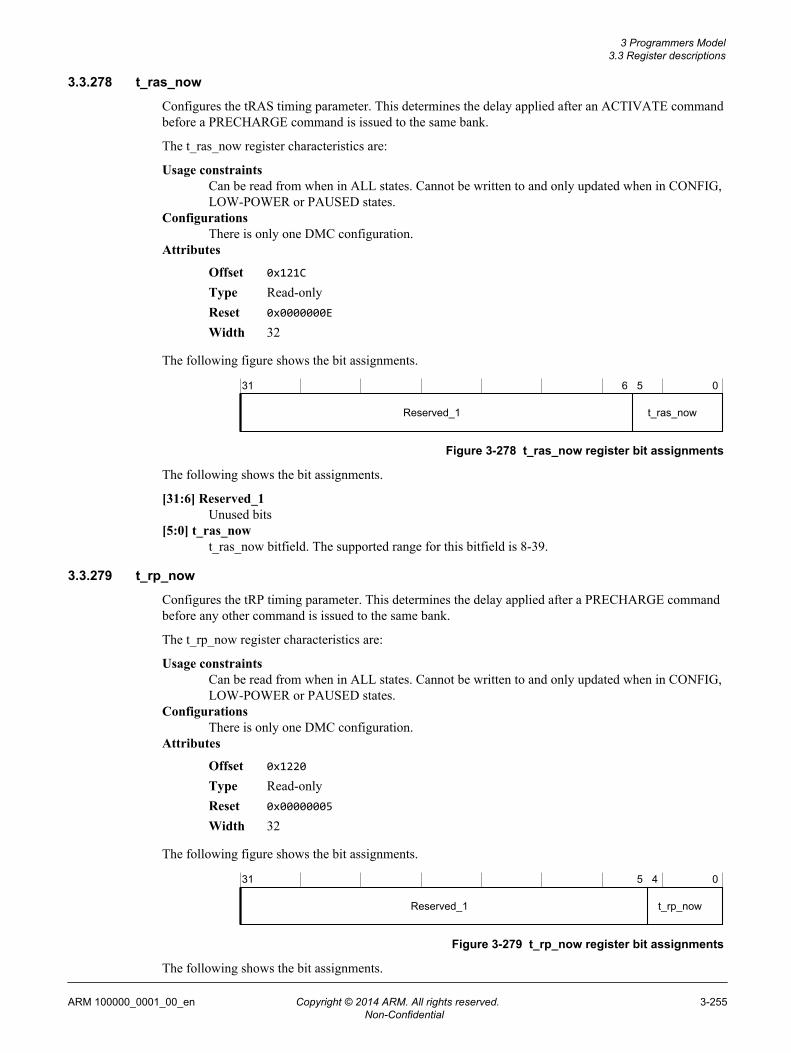
3.3.278 t_ras_now
Configures the tRAS timing parameter. This determines the delay applied after an ACTIVATE commandbefore a PRECHARGE command is issued to the same bank.
The t_ras_now register characteristics are:
Usage constraintsCan be read from when in ALL states. Cannot be written to and only updated when in CONFIG,LOW-POWER or PAUSED states.
ConfigurationsThere is only one DMC configuration.
Attributes
Offset 0x121C
Type Read-onlyReset 0x0000000E
Width 32
The following figure shows the bit assignments.
31 6 5 0
t_ras_nowReserved_1
Figure 3-278 t_ras_now register bit assignments
The following shows the bit assignments.
[31:6] Reserved_1Unused bits
[5:0] t_ras_nowt_ras_now bitfield. The supported range for this bitfield is 8-39.
3.3.279 t_rp_now
Configures the tRP timing parameter. This determines the delay applied after a PRECHARGE commandbefore any other command is issued to the same bank.
The t_rp_now register characteristics are:
Usage constraintsCan be read from when in ALL states. Cannot be written to and only updated when in CONFIG,LOW-POWER or PAUSED states.
ConfigurationsThere is only one DMC configuration.
Attributes
Offset 0x1220
Type Read-onlyReset 0x00000005
Width 32
The following figure shows the bit assignments.
31 5 4 0
t_rp_nowReserved_1
Figure 3-279 t_rp_now register bit assignments
The following shows the bit assignments.
3 Programmers Model3.3 Register descriptions
ARM 100000_0001_00_en Copyright © 2014 ARM. All rights reserved. 3-255Non-Confidential

[31:5] Reserved_1Unused bits
[4:0] t_rp_nowt_rp_now bitfield. The supported range for this bitfield is 4-18.
3.3.280 t_rpall_now
Configures the tRPALL timing parameter. This determines the delay applied after a PRECHARGEALLcommand before any other command is issued to the same rank.
The t_rpall_now register characteristics are:
Usage constraintsCan be read from when in ALL states. Cannot be written to and only updated when in CONFIG,LOW-POWER or PAUSED states.
ConfigurationsThere is only one DMC configuration.
Attributes
Offset 0x1224
Type Read-onlyReset 0x00000005
Width 32
The following figure shows the bit assignments.
31 5 4 0
t_rpall_nowReserved_1
Figure 3-280 t_rpall_now register bit assignments
The following shows the bit assignments.
[31:5] Reserved_1Unused bits
[4:0] t_rpall_nowt_rpall_now bitfield. The supported range for this bitfield is 4-18.
3.3.281 t_rrd_now
Configures the tRRD timing parameter. This determines the delay applied after an ACTIVATEcommand before another ACTIVATE command is issued to the same rank. The _l and _s fields apply tothe same bank group, and a different bank group, respectively, as described in the DDR4 specification.
The t_rrd_now register characteristics are:
Usage constraintsCan be read from when in ALL states. Cannot be written to and only updated when in CONFIG,LOW-POWER or PAUSED states.
ConfigurationsThere is only one DMC configuration.
Attributes
Offset 0x1228
Type Read-onlyReset 0x00000404
Width 32
The following figure shows the bit assignments.
3 Programmers Model3.3 Register descriptions
ARM 100000_0001_00_en Copyright © 2014 ARM. All rights reserved. 3-256Non-Confidential

31 20 19 16 15 12 11 8 7 4 3 0
Reserved_3
t_rrd_l_nowReserved_1t_rrd_s_now
Reserved_2t_rrd_cs_now
Figure 3-281 t_rrd_now register bit assignments
The following shows the bit assignments.
[31:20] Reserved_3Unused bits
[19:16] t_rrd_cs_nowt_rrd_cs_now bitfield. The supported range for this bitfield is 0-15.
[15:12] Reserved_2Unused bits
[11:8] t_rrd_l_nowt_rrd_l_now bitfield. The supported range for this bitfield is 1-15.
[7:4] Reserved_1Unused bits
[3:0] t_rrd_s_nowt_rrd_s_now bitfield. The supported range for this bitfield is 1-15.
3.3.282 t_act_window_now
Configures the tFAW and tMAWi timing parameters.
The t_act_window_now register characteristics are:
Usage constraintsCan be read from when in ALL states. Cannot be written to and only updated when in CONFIG,LOW-POWER or PAUSED states.
ConfigurationsThere is only one DMC configuration.
Attributes
Offset 0x122C
Type Read-onlyReset 0x03560014
Width 32
The following figure shows the bit assignments.
31 26 25 16 15 6 5 0
t_faw_nowReserved_1t_mawi_nowReserved_2
Figure 3-282 t_act_window_now register bit assignments
The following shows the bit assignments.
[31:26] Reserved_2Unused bits
[25:16] t_mawi_nowSets the value of the average delay required between ACTIVATE commands to the same row tonot violate tMAC in tMAW. Must be programmed to (tMAW/(tMAC/2)).
3 Programmers Model3.3 Register descriptions
ARM 100000_0001_00_en Copyright © 2014 ARM. All rights reserved. 3-257Non-Confidential

[15:6] Reserved_1Unused bits
[5:0] t_faw_nowThe DMC does not issue more than 4 ACTIVATE commands within a rolling tFAW window.The supported range for this bitfield is 8-63.
3.3.283 t_rtr_now
Configures the read-to-read timing parameter. This determines the READ to READ command delayapplied between reads to the same chip, other bank group (t_rtr_s), same chip, same bank group (t_rtr_l),and different chip-selects (t_rtr_cs).
The t_rtr_now register characteristics are:
Usage constraintsCan be read from when in ALL states. Cannot be written to and only updated when in CONFIG,LOW-POWER or PAUSED states.
ConfigurationsThere is only one DMC configuration.
Attributes
Offset 0x1234
Type Read-onlyReset 0x00060404
Width 32
The following figure shows the bit assignments.
31 25 24 23 21 20 16 15 13 12 8 7 5 4 0
t_rtr_s_nowt_rtr_l_nowReserved_4
t_rtr_cs_nowReserved_2Reserved_1
Reserved_3t_rtr_skip_now
Figure 3-283 t_rtr_now register bit assignments
The following shows the bit assignments.
[31:25] Reserved_4Unused bits
[24] t_rtr_skip_nowEnable when using 2tck preamble to prevent transactions being spaced by t_rtr + 1.
[23:21] Reserved_3Unused bits
[20:16] t_rtr_cs_nowt_rtr_cs_now bitfield. The supported range for this bitfield is 6-31.
[15:13] Reserved_2Unused bits
[12:8] t_rtr_l_nowt_rtr_l_now bitfield. The supported range for this bitfield is 4-31.
[7:5] Reserved_1Unused bits
[4:0] t_rtr_s_nowt_rtr_s_now bitfield. The supported range for this bitfield is 4-31.
3 Programmers Model3.3 Register descriptions
ARM 100000_0001_00_en Copyright © 2014 ARM. All rights reserved. 3-258Non-Confidential

3.3.284 t_rtw_now
Configures the read-to-write timing parameter. This determines the READ to WRITE command delayapplied between issued commands to the same chip, other bank group (t_rtw_s), same chip, same bankgroup (t_trw_l), and other chip-selects (t_rtw_cs).
The t_rtw_now register characteristics are:
Usage constraintsCan be read from when in ALL states. Cannot be written to and only updated when in CONFIG,LOW-POWER or PAUSED states.
ConfigurationsThere is only one DMC configuration.
Attributes
Offset 0x1238
Type Read-onlyReset 0x00060606
Width 32
The following figure shows the bit assignments.
31 21 20 16 15 13 12 8 7 5 4 0
t_rtw_l_nowReserved_3
Reserved_2Reserved_1t_rtw_s_now
t_rtw_cs_now
Figure 3-284 t_rtw_now register bit assignments
The following shows the bit assignments.
[31:21] Reserved_3Unused bits
[20:16] t_rtw_cs_nowt_rtw_cs_now bitfield. The supported range for this bitfield is 4-31.
[15:13] Reserved_2Unused bits
[12:8] t_rtw_l_nowt_rtw_l_now bitfield. The supported range for this bitfield is 4-31.
[7:5] Reserved_1Unused bits
[4:0] t_rtw_s_nowt_rtw_s_now bitfield. The supported range for this bitfield is 4-31.
3.3.285 t_rtp_now
Configures the read-to-precharge timing parameter. This determines the READ to PRECHARGEcommand delay applied between issued commands to the same bank.
The t_rtp_now register characteristics are:
Usage constraintsCan be read from when in ALL states. Cannot be written to and only updated when in CONFIG,LOW-POWER or PAUSED states.
ConfigurationsThere is only one DMC configuration.
Attributes
3 Programmers Model3.3 Register descriptions
ARM 100000_0001_00_en Copyright © 2014 ARM. All rights reserved. 3-259Non-Confidential

Offset 0x123C
Type Read-onlyReset 0x00000004
Width 32
The following figure shows the bit assignments.
31 4 3 0
t_rtp_nowReserved_1
Figure 3-285 t_rtp_now register bit assignments
The following shows the bit assignments.
[31:4] Reserved_1Unused bits
[3:0] t_rtp_nowt_rtp_now bitfield. The supported range for this bitfield is 4-15.
3.3.286 t_wr_now
Configures the tWR timing parameter. This determines the write recovery time and is used as the delayapplied between the issue of a WRITE command and subsequent commands, other than WRITEs, to thesame bank. This must take into account CRC timing requirements.
The t_wr_now register characteristics are:
Usage constraintsCan be read from when in ALL states. Cannot be written to and only updated when in CONFIG,LOW-POWER or PAUSED states.
ConfigurationsThere is only one DMC configuration.
Attributes
Offset 0x1244
Type Read-onlyReset 0x00000005
Width 32
The following figure shows the bit assignments.
31 6 5 0
t_wr_nowReserved_1
Figure 3-286 t_wr_now register bit assignments
The following shows the bit assignments.
[31:6] Reserved_1Unused bits
[5:0] t_wr_nowt_wr_now bitfield. The supported range for this bitfield is 5-63.
3 Programmers Model3.3 Register descriptions
ARM 100000_0001_00_en Copyright © 2014 ARM. All rights reserved. 3-260Non-Confidential

3.3.287 t_wtr_now
Configures the write-to-read timing parameter, for both same chip, other bank group (tWTR_s), samechip, same bank group (t_WTR_l), and alternate chip (tWTR_cs). These must take into account CRCtiming requirements.
The t_wtr_now register characteristics are:
Usage constraintsCan be read from when in ALL states. Cannot be written to and only updated when in CONFIG,LOW-POWER or PAUSED states.
ConfigurationsThere is only one DMC configuration.
Attributes
Offset 0x1248
Type Read-onlyReset 0x00040505
Width 32
The following figure shows the bit assignments.
31 22 21 16 15 14 13 8 7 6 5 0
t_wtr_s_nowt_wtr_l_nowt_wtr_cs_nowReserved_3
Reserved_2Reserved_1
Figure 3-287 t_wtr_now register bit assignments
The following shows the bit assignments.
[31:22] Reserved_3Unused bits
[21:16] t_wtr_cs_nowt_wtr_cs_now bitfield. The supported range for this bitfield is 2-63.
[15:14] Reserved_2Unused bits
[13:8] t_wtr_l_nowt_wtr_l_now bitfield. The supported range for this bitfield is 5-63.
[7:6] Reserved_1Unused bits
[5:0] t_wtr_s_nowt_wtr_s_now bitfield. The supported range for this bitfield is 5-63.
3.3.288 t_wtw_now
Configures the write-to-write timing parameter for same chip, other bank group (t_wtw_s), same chip,same bank group (t_wtw_l), alternate chip (t_wtw_cs) writes. These must take into account CRC timingrequirements.
The t_wtw_now register characteristics are:
Usage constraintsCan be read from when in ALL states. Cannot be written to and only updated when in CONFIG,LOW-POWER or PAUSED states.
ConfigurationsThere is only one DMC configuration.
Attributes
Offset 0x124C
3 Programmers Model3.3 Register descriptions
ARM 100000_0001_00_en Copyright © 2014 ARM. All rights reserved. 3-261Non-Confidential

Type Read-onlyReset 0x00060404
Width 32
The following figure shows the bit assignments.
31 25 24 23 22 21 16 15 14 13 8 7 6 5 0
t_wtw_s_nowt_wtw_l_nowt_wtw_cs_nowReserved_4
Reserved_3Reserved_2Reserved_1
t_wtw_skip_now
Figure 3-288 t_wtw_now register bit assignments
The following shows the bit assignments.
[31:25] Reserved_4Unused bits
[24] t_wtw_skip_nowEnable when using 2tck preamble to prevent transactions being spaced by t_wtw + 1.
[23:22] Reserved_3Unused bits
[21:16] t_wtw_cs_nowt_wtw_cs_now bitfield. The supported range for this bitfield is 6-35.
[15:14] Reserved_2Unused bits
[13:8] t_wtw_l_nowt_wtw_l_now bitfield. The supported range for this bitfield is 4-35.
[7:6] Reserved_1Unused bits
[5:0] t_wtw_s_nowt_wtw_s_now bitfield. The supported range for this bitfield is 4-35.
3.3.289 t_xmpd_now
Configures the command delay between exiting Maximum Power Down and a subsequent command tothat rank.
The t_xmpd_now register characteristics are:
Usage constraintsCan be read from when in ALL states. Cannot be written to and only updated when in CONFIG,LOW-POWER or PAUSED states.
ConfigurationsThere is only one DMC configuration.
Attributes
Offset 0x1254
Type Read-onlyReset 0x000003FF
Width 32
The following figure shows the bit assignments.
3 Programmers Model3.3 Register descriptions
ARM 100000_0001_00_en Copyright © 2014 ARM. All rights reserved. 3-262Non-Confidential

31 12 11 0
t_xmpd_nowReserved_1
Figure 3-289 t_xmpd_now register bit assignments
The following shows the bit assignments.
[31:12] Reserved_1Unused bits
[11:0] t_xmpd_nowt_xmpd_now bitfield. The supported range for this bitfield is 1-4094.
3.3.290 t_ep_now
Configures the enter power-down timing parameter. This parameter is applied between the issue of anactive or precharge power down request and subsequent commands to the same rank.
The t_ep_now register characteristics are:
Usage constraintsCan be read from when in ALL states. Cannot be written to and only updated when in CONFIG,LOW-POWER or PAUSED states.
ConfigurationsThere is only one DMC configuration.
Attributes
Offset 0x1258
Type Read-onlyReset 0x00000002
Width 32
The following figure shows the bit assignments.
31 8 7 0
t_ep_nowReserved_1
Figure 3-290 t_ep_now register bit assignments
The following shows the bit assignments.
[31:8] Reserved_1Unused bits
[7:0] t_ep_nowt_ep_now bitfield. The supported range for this bitfield is 1-255.
3.3.291 t_xp_now
Configures the exit power-down timing parameter for operations that do not require a DLL (tXP), andthose that do (tXPDLL). t_xpdll must be greater than or equal to tRCD and tCKE. t_xp must be greaterthan or equal to tMPX_S.
The t_xp_now register characteristics are:
Usage constraintsCan be read from when in ALL states. Cannot be written to and only updated when in CONFIG,LOW-POWER or PAUSED states.
ConfigurationsThere is only one DMC configuration.
Attributes
3 Programmers Model3.3 Register descriptions
ARM 100000_0001_00_en Copyright © 2014 ARM. All rights reserved. 3-263Non-Confidential
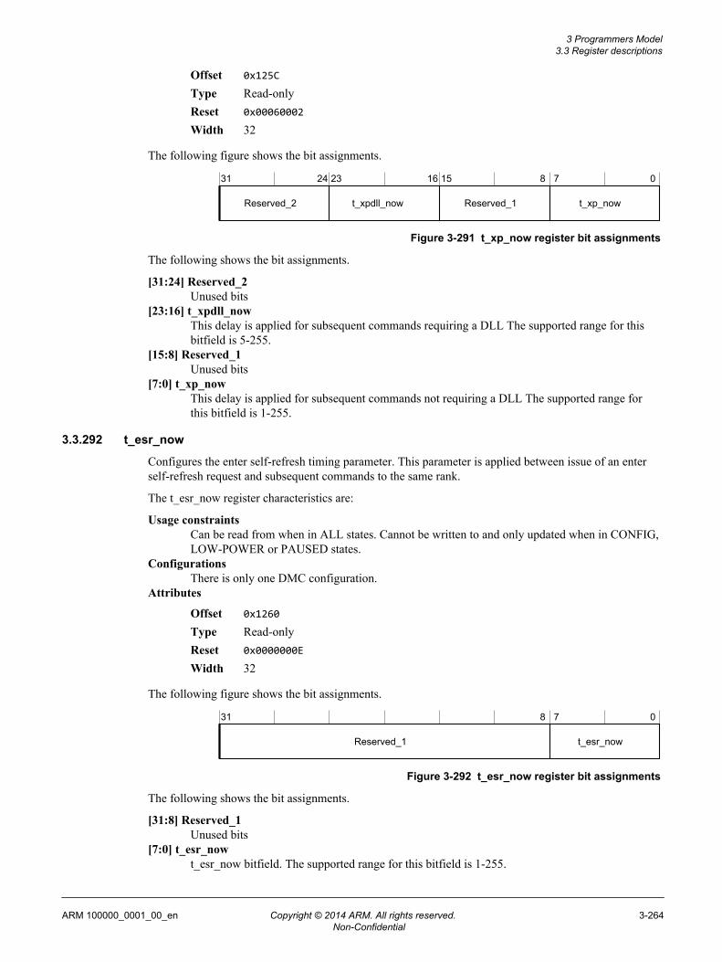
Offset 0x125C
Type Read-onlyReset 0x00060002
Width 32
The following figure shows the bit assignments.
31 24 23 16 15 8 7 0
t_xp_nowReserved_1t_xpdll_nowReserved_2
Figure 3-291 t_xp_now register bit assignments
The following shows the bit assignments.
[31:24] Reserved_2Unused bits
[23:16] t_xpdll_nowThis delay is applied for subsequent commands requiring a DLL The supported range for thisbitfield is 5-255.
[15:8] Reserved_1Unused bits
[7:0] t_xp_nowThis delay is applied for subsequent commands not requiring a DLL The supported range forthis bitfield is 1-255.
3.3.292 t_esr_now
Configures the enter self-refresh timing parameter. This parameter is applied between issue of an enterself-refresh request and subsequent commands to the same rank.
The t_esr_now register characteristics are:
Usage constraintsCan be read from when in ALL states. Cannot be written to and only updated when in CONFIG,LOW-POWER or PAUSED states.
ConfigurationsThere is only one DMC configuration.
Attributes
Offset 0x1260
Type Read-onlyReset 0x0000000E
Width 32
The following figure shows the bit assignments.
31 8 7 0
t_esr_nowReserved_1
Figure 3-292 t_esr_now register bit assignments
The following shows the bit assignments.
[31:8] Reserved_1Unused bits
[7:0] t_esr_nowt_esr_now bitfield. The supported range for this bitfield is 1-255.
3 Programmers Model3.3 Register descriptions
ARM 100000_0001_00_en Copyright © 2014 ARM. All rights reserved. 3-264Non-Confidential

3.3.293 t_xsr_now
Configures the exit self-refresh timing parameter. This parameter is applied between the issue of an exitself-refresh request and subsequent commands to the same rank.
The t_xsr_now register characteristics are:
Usage constraintsCan be read from when in ALL states. Cannot be written to and only updated when in CONFIG,LOW-POWER or PAUSED states.
ConfigurationsThere is only one DMC configuration.
Attributes
Offset 0x1264
Type Read-onlyReset 0x05120100
Width 32
The following figure shows the bit assignments.
31 27 26 16 15 10 9 0
t_xsr_nowReserved_1t_xsrdll_nowReserved_2
Figure 3-293 t_xsr_now register bit assignments
The following shows the bit assignments.
[31:27] Reserved_2Unused bits
[26:16] t_xsrdll_nowThis delay is applied for subsequent commands requiring a DLL. The supported range for thisbitfield is 1-2047.
[15:10] Reserved_1Unused bits
[9:0] t_xsr_nowThis delay is applied for subsequent commands not requiring a DLL. The supported range forthis bitfield is 1-1023.
3.3.294 t_esrck_now
Configures the delay between entering self-refresh and disabling the DRAM clock. This parameter isapplied when stopping the clock when in self-refresh and when in a maximum power-down state.
The t_esrck_now register characteristics are:
Usage constraintsCan be read from when in ALL states. Cannot be written to and only updated when in CONFIG,LOW-POWER or PAUSED states.
ConfigurationsThere is only one DMC configuration.
Attributes
Offset 0x1268
Type Read-onlyReset 0x00000005
Width 32
The following figure shows the bit assignments.
3 Programmers Model3.3 Register descriptions
ARM 100000_0001_00_en Copyright © 2014 ARM. All rights reserved. 3-265Non-Confidential

31 5 4 0
t_esrck_nowReserved_1
Figure 3-294 t_esrck_now register bit assignments
The following shows the bit assignments.
[31:5] Reserved_1Unused bits
[4:0] t_esrck_nowt_esrck_now bitfield. The supported range for this bitfield is 1-31.
3.3.295 t_ckxsr_now
Configures the delay between DRAM clock enable and exiting self-refresh. This parameter is appliedwhen re-instating the clock when in self-refresh and when in a maximum power-down state.
The t_ckxsr_now register characteristics are:
Usage constraintsCan be read from when in ALL states. Cannot be written to and only updated when in CONFIG,LOW-POWER or PAUSED states.
ConfigurationsThere is only one DMC configuration.
Attributes
Offset 0x126C
Type Read-onlyReset 0x00000001
Width 32
The following figure shows the bit assignments.
31 5 4 0
Reserved_1
t_ckxsr_now
Figure 3-295 t_ckxsr_now register bit assignments
The following shows the bit assignments.
[31:5] Reserved_1Unused bits
[4:0] t_ckxsr_nowt_ckxsr_now bitfield. The supported range for this bitfield is 1-31.
3.3.296 t_cmd_now
Configures command signalling timing.
The t_cmd_now register characteristics are:
Usage constraintsCan be read from when in ALL states. Cannot be written to and only updated when in CONFIG,LOW-POWER or PAUSED states.
ConfigurationsThere is only one DMC configuration.
Attributes
Offset 0x1270
3 Programmers Model3.3 Register descriptions
ARM 100000_0001_00_en Copyright © 2014 ARM. All rights reserved. 3-266Non-Confidential

Type Read-onlyReset 0x00000000
Width 32
The following figure shows the bit assignments.
31 12 11 8 7 4 3 0
Reserved_2
t_cal_nowReserved_1t_cmd_lat_now
Figure 3-296 t_cmd_now register bit assignments
The following shows the bit assignments.
[31:12] Reserved_2Unused bits
[11:8] t_cal_nowSpecifies the Command Address latency at the DDR4 device. The supported range for thisbitfield is 0-10.
Note
t_cal must be zero when you use RDIMMs.
[7:4] Reserved_1Unused bits
[3:0] t_cmd_lat_nowSpecifies the number of DFI clocks after the dfi_cs_n signal is asserted until the associatedcommand and address bus is driven. The supported range for this bitfield is 0-10.
3.3.297 t_parity_now
Parity latencies t_parinlat and t_completion.
The t_parity_now register characteristics are:
Usage constraintsCan be read from when in ALL states. Cannot be written to and only updated when in CONFIG,LOW-POWER or PAUSED states.
ConfigurationsThere is only one DMC configuration.
Attributes
Offset 0x1274
Type Read-onlyReset 0x00000900
Width 32
The following figure shows the bit assignments.
31 14 13 8 7 2 1 0
Reserved_1Reserved_2
t_completion_nowt_parin_lat_now
Figure 3-297 t_parity_now register bit assignments
3 Programmers Model3.3 Register descriptions
ARM 100000_0001_00_en Copyright © 2014 ARM. All rights reserved. 3-267Non-Confidential

The following shows the bit assignments.
[31:14] Reserved_2Unused bits
[13:8] t_completion_nowDetermines the DMC clock cycle delay between when the dfi_cs_n signal is asserted and thecycle in which that command can be considered complete. In programming this value, you mustconsider the DFI timing parameters t_wrdata_delay, t_error_resp, t_crcmax_lat, andt_phyrdlatmax to ensure all have expired, where applicable, within t_completion cycles. Thesupported range for this bitfield is 9-60.
[7:2] Reserved_1Unused bits
[1:0] t_parin_lat_nowSpecifies the number of DFI clocks between when the dfi_cs_n signal is asserted and when theassociated dfi_parity_in signal is driven. The supported range for this bitfield is 0-3.
3.3.298 t_zqcs_now
Configures the delay to apply following a ZQC-Short calibration command.
The t_zqcs_now register characteristics are:
Usage constraintsCan be read from when in ALL states. Cannot be written to and only updated when in CONFIG,LOW-POWER or PAUSED states.
ConfigurationsThere is only one DMC configuration.
Attributes
Offset 0x1278
Type Read-onlyReset 0x00000040
Width 32
The following figure shows the bit assignments.
31 10 9 0
t_zqcs_nowReserved_1
Figure 3-298 t_zqcs_now register bit assignments
The following shows the bit assignments.
[31:10] Reserved_1Unused bits
[9:0] t_zqcs_nowt_zqcs_now bitfield. The supported range for this bitfield is 2-1023.
3.3.299 t_rddata_en_now
Determines the time between a READ command commencing on the DFI interface, and the assertion ofthe dfi_read_en signal.
The t_rddata_en_now register characteristics are:
Usage constraintsCan be read from when in ALL states. Cannot be written to and only updated when in CONFIG,LOW-POWER or PAUSED states.
ConfigurationsThere is only one DMC configuration.
3 Programmers Model3.3 Register descriptions
ARM 100000_0001_00_en Copyright © 2014 ARM. All rights reserved. 3-268Non-Confidential

Attributes
Offset 0x1300
Type Read-onlyReset 0x00000001
Width 32
The following figure shows the bit assignments.
31 21 20 16 15 14 13 8 7 6 5 0
Reserved_3
t_rddata_en_diff_nowReserved_1t_rddata_en_now
Reserved_2t_phyrdcslat_now
Figure 3-299 t_rddata_en_now register bit assignments
The following shows the bit assignments.
[31:21] Reserved_3Unused bits
[20:16] t_phyrdcslat_nowSpecifies the number of DFI PHY clocks between a READ command commencing on the DFIinterface (assertion of chip-select), and when the associated dfi_rddata_cs_n signal is asserted.The supported range for this bitfield is 0-31.
[15:14] Reserved_2Unused bits
[13:8] t_rddata_en_diff_nowDescribes a PHY specific value useful for aligning t_rddata_en for a specific PHY. This valuehas no effect on the controller. The supported range for this bitfield is 0-40.
[7:6] Reserved_1Unused bits
[5:0] t_rddata_en_nowt_rddata_en_now bitfield. The supported range for this bitfield is 0-40.
3.3.300 t_phyrdlat_now
Determines the maximum possible time between the assertion of the dfi_read_en signal, and theassertion of the dfi_rddata_valid signal by the PHY.
The t_phyrdlat_now register characteristics are:
Usage constraintsCan be read from when in ALL states. Cannot be written to and only updated when in CONFIG,LOW-POWER or PAUSED states.
ConfigurationsThere is only one DMC configuration.
Attributes
Offset 0x1304
Type Read-onlyReset 0x00000000
Width 32
The following figure shows the bit assignments.
3 Programmers Model3.3 Register descriptions
ARM 100000_0001_00_en Copyright © 2014 ARM. All rights reserved. 3-269Non-Confidential

31 6 5 0
Reserved_1
t_phyrdlat_now
Figure 3-300 t_phyrdlat_now register bit assignments
The following shows the bit assignments.
[31:6] Reserved_1Unused bits
[5:0] t_phyrdlat_nowDetermines the maximum time between the assertion of the dfi_read_en signal and the assertionof the dfi_rddata_valid signal by the PHY. The supported range for this bitfield is 2-62.
3.3.301 t_phywrlat_now
Determines the time between a WRITE command commencing on the DFI interface, and the assertion ofthe dfi_wrdata_en, dfi_wrdata_cs and dfi_wrdata signals.
The t_phywrlat_now register characteristics are:
Usage constraintsCan be read from when in ALL states. Cannot be written to and only updated when in CONFIG,LOW-POWER or PAUSED states.
ConfigurationsThere is only one DMC configuration.
Attributes
Offset 0x1308
Type Read-onlyReset 0x00000001
Width 32
The following figure shows the bit assignments.
31 25 24 23 21 20 16 15 13 12 8 7 5 4 0
Reserved_4
t_phywrlat_diff_nowReserved_1t_phywrlat_now
Reserved_2t_phywrcslat_now
t_phywrdata_nowReserved_3
Figure 3-301 t_phywrlat_now register bit assignments
The following shows the bit assignments.
[31:25] Reserved_4Unused bits
[24] t_phywrdata_nowDetermines the time between the assertion of the dfi_wrdata_en and dfi_wrdata signals. Thesupported range for this bitfield is 0-1.
[23:21] Reserved_3Unused bits
3 Programmers Model3.3 Register descriptions
ARM 100000_0001_00_en Copyright © 2014 ARM. All rights reserved. 3-270Non-Confidential

[20:16] t_phywrcslat_nowSpecifies the number of DFI PHY clocks between when a write command is sent on the DFIcontrol interface (dfi_cs_n assertion) and when the associated dfi_wrdata_cs_n signal isasserted. The supported range for this bitfield is 0-31.
[15:13] Reserved_2Unused bits
[12:8] t_phywrlat_diff_nowDescribes the PHY specific value useful for aligning t_phywrlat for a specific PHY. This valuehas no effect on the controller. The supported range for this bitfield is 0-31.
[7:5] Reserved_1Unused bits
[4:0] t_phywrlat_nowDetermines the time between a WRITE command commencing on the DFI interface, and theassertion of the dfi_wrdata_en signal. The supported range for this bitfield is 0-31.
3.3.302 rdlvl_control_now
Determines the DMC behavior during read training operations. See the PHY training interface section ofthe Integration Manual for more details on PHY training.
The rdlvl_control_now register characteristics are:
Usage constraintsCan be read from when in ALL states. Cannot be written to and only updated when in CONFIG,LOW-POWER or PAUSED states.
ConfigurationsThere is only one DMC configuration.
Attributes
Offset 0x1310
Type Read-onlyReset 0x00001080
Width 32
The following figure shows the bit assignments.
31 25 24 23 20 19 16 15 14 13 12 11 10 9 8 7 5 4 3 1 0
Reserved_7
rdlvl_setup_nowReserved_1rdlvl_mode_now
Reserved_2Reserved_3
rdlvl_refresh_nowReserved_4rdlvl_command_ba1_0_now
Reserved_5rdlvl_err_en_nowrefresh_dur_rdlvl_now
rdlvl_pattern_nowReserved_6rdlvl_preamble_now
Figure 3-302 rdlvl_control_now register bit assignments
The following shows the bit assignments.
[31:25] Reserved_7Unused bits
3 Programmers Model3.3 Register descriptions
ARM 100000_0001_00_en Copyright © 2014 ARM. All rights reserved. 3-271Non-Confidential
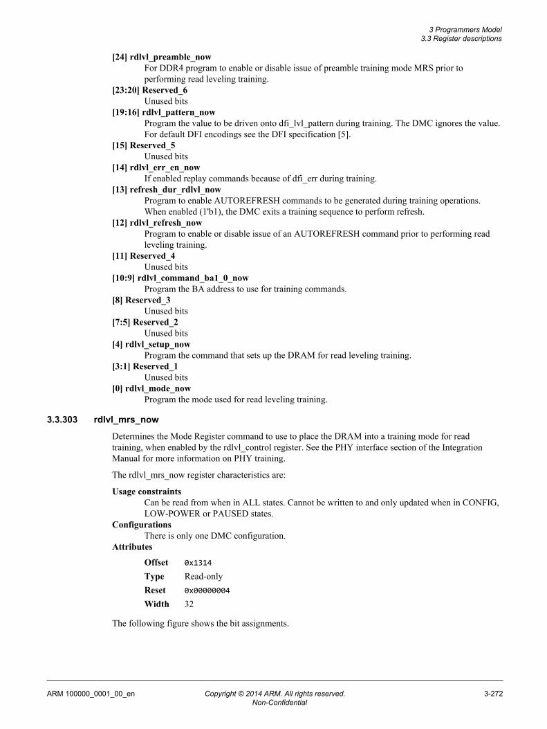
[24] rdlvl_preamble_nowFor DDR4 program to enable or disable issue of preamble training mode MRS prior toperforming read leveling training.
[23:20] Reserved_6Unused bits
[19:16] rdlvl_pattern_nowProgram the value to be driven onto dfi_lvl_pattern during training. The DMC ignores the value.For default DFI encodings see the DFI specification [5].
[15] Reserved_5Unused bits
[14] rdlvl_err_en_nowIf enabled replay commands because of dfi_err during training.
[13] refresh_dur_rdlvl_nowProgram to enable AUTOREFRESH commands to be generated during training operations.When enabled (1'b1), the DMC exits a training sequence to perform refresh.
[12] rdlvl_refresh_nowProgram to enable or disable issue of an AUTOREFRESH command prior to performing readleveling training.
[11] Reserved_4Unused bits
[10:9] rdlvl_command_ba1_0_nowProgram the BA address to use for training commands.
[8] Reserved_3Unused bits
[7:5] Reserved_2Unused bits
[4] rdlvl_setup_nowProgram the command that sets up the DRAM for read leveling training.
[3:1] Reserved_1Unused bits
[0] rdlvl_mode_nowProgram the mode used for read leveling training.
3.3.303 rdlvl_mrs_now
Determines the Mode Register command to use to place the DRAM into a training mode for readtraining, when enabled by the rdlvl_control register. See the PHY interface section of the IntegrationManual for more information on PHY training.
The rdlvl_mrs_now register characteristics are:
Usage constraintsCan be read from when in ALL states. Cannot be written to and only updated when in CONFIG,LOW-POWER or PAUSED states.
ConfigurationsThere is only one DMC configuration.
Attributes
Offset 0x1314
Type Read-onlyReset 0x00000004
Width 32
The following figure shows the bit assignments.
3 Programmers Model3.3 Register descriptions
ARM 100000_0001_00_en Copyright © 2014 ARM. All rights reserved. 3-272Non-Confidential
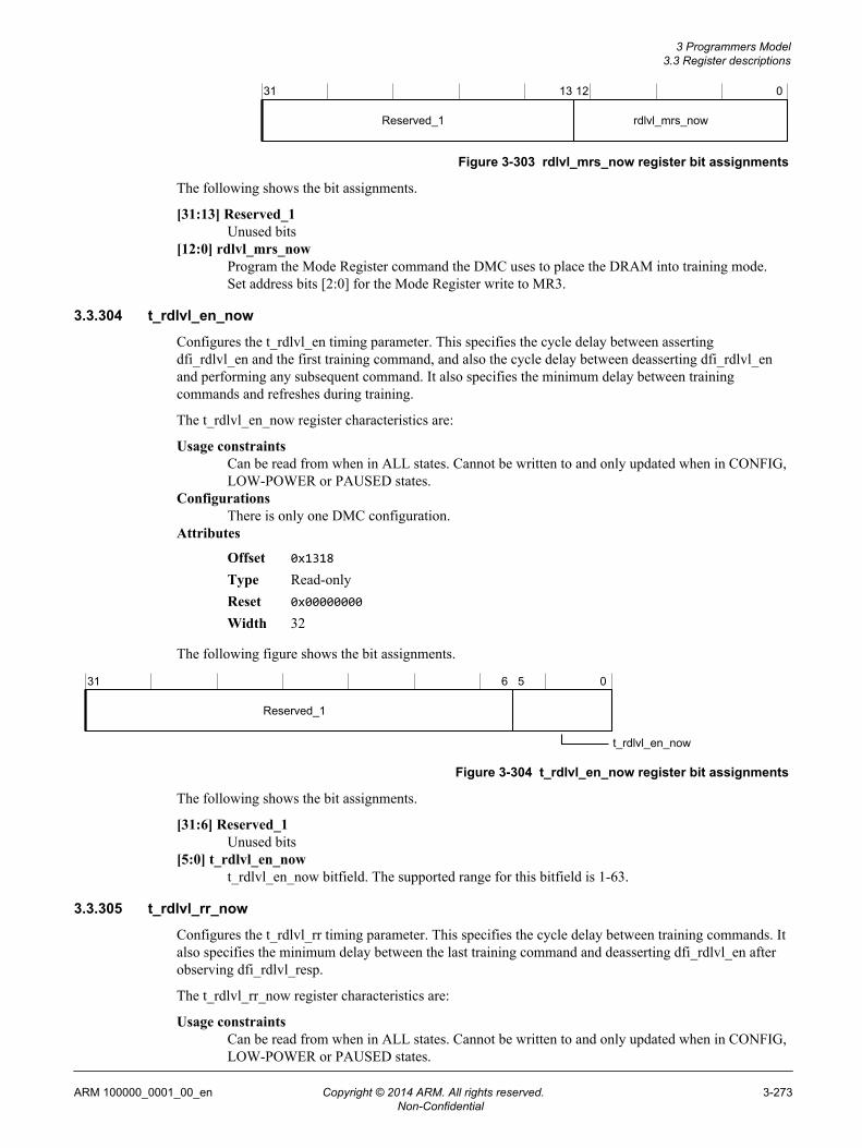
31 13 12 0
rdlvl_mrs_nowReserved_1
Figure 3-303 rdlvl_mrs_now register bit assignments
The following shows the bit assignments.
[31:13] Reserved_1Unused bits
[12:0] rdlvl_mrs_nowProgram the Mode Register command the DMC uses to place the DRAM into training mode.Set address bits [2:0] for the Mode Register write to MR3.
3.3.304 t_rdlvl_en_now
Configures the t_rdlvl_en timing parameter. This specifies the cycle delay between assertingdfi_rdlvl_en and the first training command, and also the cycle delay between deasserting dfi_rdlvl_enand performing any subsequent command. It also specifies the minimum delay between trainingcommands and refreshes during training.
The t_rdlvl_en_now register characteristics are:
Usage constraintsCan be read from when in ALL states. Cannot be written to and only updated when in CONFIG,LOW-POWER or PAUSED states.
ConfigurationsThere is only one DMC configuration.
Attributes
Offset 0x1318
Type Read-onlyReset 0x00000000
Width 32
The following figure shows the bit assignments.
31 6 5 0
Reserved_1
t_rdlvl_en_now
Figure 3-304 t_rdlvl_en_now register bit assignments
The following shows the bit assignments.
[31:6] Reserved_1Unused bits
[5:0] t_rdlvl_en_nowt_rdlvl_en_now bitfield. The supported range for this bitfield is 1-63.
3.3.305 t_rdlvl_rr_now
Configures the t_rdlvl_rr timing parameter. This specifies the cycle delay between training commands. Italso specifies the minimum delay between the last training command and deasserting dfi_rdlvl_en afterobserving dfi_rdlvl_resp.
The t_rdlvl_rr_now register characteristics are:
Usage constraintsCan be read from when in ALL states. Cannot be written to and only updated when in CONFIG,LOW-POWER or PAUSED states.
3 Programmers Model3.3 Register descriptions
ARM 100000_0001_00_en Copyright © 2014 ARM. All rights reserved. 3-273Non-Confidential

ConfigurationsThere is only one DMC configuration.
Attributes
Offset 0x131C
Type Read-onlyReset 0x00000000
Width 32
The following figure shows the bit assignments.
31 10 9 0
t_rdlvl_rr_nowReserved_1
Figure 3-305 t_rdlvl_rr_now register bit assignments
The following shows the bit assignments.
[31:10] Reserved_1Unused bits
[9:0] t_rdlvl_rr_nowt_rdlvl_rr_now bitfield. The supported range for this bitfield is 4-1023.
3.3.306 wrlvl_control_now
Determines the DMC behavior during write training operations. See the PHY training interface sectionof the Integration Manual for more information on PHY training.
The wrlvl_control_now register characteristics are:
Usage constraintsCan be read from when in ALL states. Cannot be written to and only updated when in CONFIG,LOW-POWER or PAUSED states.
ConfigurationsThere is only one DMC configuration.
Attributes
Offset 0x1320
Type Read-onlyReset 0x00001000
Width 32
The following figure shows the bit assignments.
3 Programmers Model3.3 Register descriptions
ARM 100000_0001_00_en Copyright © 2014 ARM. All rights reserved. 3-274Non-Confidential

31 20 19 16 15 14 13 12 11 10 9 8 7 5 4 3 1 0
Reserved_7
wrlvl_setup_nowReserved_1wrlvl_mode_now
Reserved_2Reserved_3
wrlvl_refresh_nowReserved_5Reserved_4
Reserved_6wrlvl_err_en_nowrefresh_dur_wrlvl_now
wrlvl_pattern_now
Figure 3-306 wrlvl_control_now register bit assignments
The following shows the bit assignments.
[31:20] Reserved_7Unused bits
[19:16] wrlvl_pattern_nowProgram the value to be driven onto dfi_lvl_pattern during training. The DMC ignores the value.For default DFI encodings see the DFI specification [5]. The supported range for this bitfield is0-15.
[15] Reserved_6Unused bits
[14] wrlvl_err_en_nowIf enabled replay commands because of dfi_err during training.
[13] refresh_dur_wrlvl_nowProgram to enable AUTOREFRESH commands to be generated during training operations.When enabled (1'b1), the DMC exits a training sequence to perform refresh.
[12] wrlvl_refresh_nowProgram to enable or disable issue of an AUTOREFRESH command prior to performing writeleveling training.
[11] Reserved_5Unused bits
[10:9] Reserved_4Unused bits
[8] Reserved_3Unused bits
[7:5] Reserved_2Unused bits
[4] wrlvl_setup_nowProgram the command that sets up the DRAM for write leveling training.
[3:1] Reserved_1Unused bits
[0] wrlvl_mode_nowProgram the mode used for write leveling training.
3.3.307 wrlvl_mrs_now
Determines the Mode Register command that the DMC must use to put the DRAM into a training modefor write levelling. You enable this function with the wrlvl_control Register. See the PHY traininginterface section of the Integration Manual for more information.
The wrlvl_mrs_now register characteristics are:
3 Programmers Model3.3 Register descriptions
ARM 100000_0001_00_en Copyright © 2014 ARM. All rights reserved. 3-275Non-Confidential

Usage constraintsCan be read from when in ALL states. Cannot be written to and only updated when in CONFIG,LOW-POWER or PAUSED states.
ConfigurationsThere is only one DMC configuration.
Attributes
Offset 0x1324
Type Read-onlyReset 0x00000086
Width 32
The following figure shows the bit assignments.
31 13 12 0
wrlvl_mrs_nowReserved_1
Figure 3-307 wrlvl_mrs_now register bit assignments
The following shows the bit assignments.
[31:13] Reserved_1Unused bits
[12:0] wrlvl_mrs_nowProgram the command the DMC uses to place the DRAM into training mode. Set address bits[12:0] for the Mode Register write to MR1.
3.3.308 t_wrlvl_en_now
Configures the t_wrlvl_en timing parameter. Specifies the cycle delay between asserting ODT fortraining and asserting dfi_wrlvl_en, the delay between asserting dfi_wrlvl_en and the first trainingcommand, the delay between deasserting dfi_wrlvl_en and de-asserting ODT, and deasserting ODT toany subsequent command. It is also used between ODT transitions and refreshes generated duringtraining.
The t_wrlvl_en_now register characteristics are:
Usage constraintsCan be read from when in ALL states. Cannot be written to and only updated when in CONFIG,LOW-POWER or PAUSED states.
ConfigurationsThere is only one DMC configuration.
Attributes
Offset 0x1328
Type Read-onlyReset 0x00000000
Width 32
The following figure shows the bit assignments.
31 6 5 0
Reserved_1
t_wrlvl_en_now
Figure 3-308 t_wrlvl_en_now register bit assignments
The following shows the bit assignments.
3 Programmers Model3.3 Register descriptions
ARM 100000_0001_00_en Copyright © 2014 ARM. All rights reserved. 3-276Non-Confidential

[31:6] Reserved_1Unused bits
[5:0] t_wrlvl_en_nowt_wrlvl_en_now bitfield. The supported range for this bitfield is 1-63.
3.3.309 t_wrlvl_ww_now
Configures the t_wrlvl_ww timing parameter. Specifies the cycle delay between training commands.Also specifies the minimum delay between the last training command and de-asserting dfi_wrlvl_en onobserving dfi_wrlvl_resp.
The t_wrlvl_ww_now register characteristics are:
Usage constraintsCan be read from when in ALL states. Cannot be written to and only updated when in CONFIG,LOW-POWER or PAUSED states.
ConfigurationsThere is only one DMC configuration.
Attributes
Offset 0x132C
Type Read-onlyReset 0x00000000
Width 32
The following figure shows the bit assignments.
31 10 9 0
t_wrlvl_ww_nowReserved_1
Figure 3-309 t_wrlvl_ww_now register bit assignments
The following shows the bit assignments.
[31:10] Reserved_1Unused bits
[9:0] t_wrlvl_ww_nowt_wrlvl_ww_now bitfield. The supported range for this bitfield is 1-1023.
3.3.310 phy_power_control_now
Configures the low-power requests made to the PHY for the different channel states.
The phy_power_control_now register characteristics are:
Usage constraintsCan be read from when in ALL states. Cannot be written to and only updated when in CONFIG,LOW-POWER or PAUSED states.
ConfigurationsThere is only one DMC configuration.
Attributes
Offset 0x1348
Type Read-onlyReset 0x00000000
Width 32
The following figure shows the bit assignments.
3 Programmers Model3.3 Register descriptions
ARM 100000_0001_00_en Copyright © 2014 ARM. All rights reserved. 3-277Non-Confidential

31 28 27 24 23 20 19 16 15 12 11 8 7 5 4 3 2 1 0
lp_sref_en_nowlp_pd_en_nowlp_idle_en_now
lp_mpd_en_nowlp_arch_en_now
lp_wakeup_pd_nowlp_wakeup_idle_nowReserved_1
lp_wakeup_arch_nowlp_wakeup_mpd_nowlp_wakeup_sref_now
Reserved_2
Figure 3-310 phy_power_control_now register bit assignments
The following shows the bit assignments.
[31:28] Reserved_2Unused bits
[27:24] lp_wakeup_arch_nowProgram the PHY wakeup encoding for PHY low-power requests when entering LOW-POWERarchitectural state. The supported range for this bitfield is 0-15.
[23:20] lp_wakeup_mpd_nowProgram the PHY wakeup encoding for PHY low-power requests when in MPD. The supportedrange for this bitfield is 0-15.
[19:16] lp_wakeup_sref_nowProgram the PHY wakeup encoding for PHY low-power requests when in self-refresh. Thesupported range for this bitfield is 0-15.
[15:12] lp_wakeup_pd_nowProgram the PHY wakeup encoding for PHY low-power requests when powered down. Thesupported range for this bitfield is 0-15.
[11:8] lp_wakeup_idle_nowProgram the PHY wakeup encoding for PHY low-power requests when idle. The supportedrange for this bitfield is 0-15.
[7:5] Reserved_1Unused bits
[4] lp_arch_en_nowProgram to enable or disable a PHY low-power request when entering LOW-POWERarchitectural state.
[3] lp_mpd_en_nowProgram to enable or disable a PHY low-power request when in MPD.
[2] lp_sref_en_nowProgram to enable or disable a PHY low-power request when in self-refresh.
[1] lp_pd_en_nowProgram to enable or disable a PHY low-power request when in power down.
[0] lp_idle_en_nowProgram to enable or disable a PHY low-power request when idle.
3.3.311 t_lpresp_now
Configures the minimum cycle delay to apply for PHY low-power handshakes.
The t_lpresp_now register characteristics are:
3 Programmers Model3.3 Register descriptions
ARM 100000_0001_00_en Copyright © 2014 ARM. All rights reserved. 3-278Non-Confidential
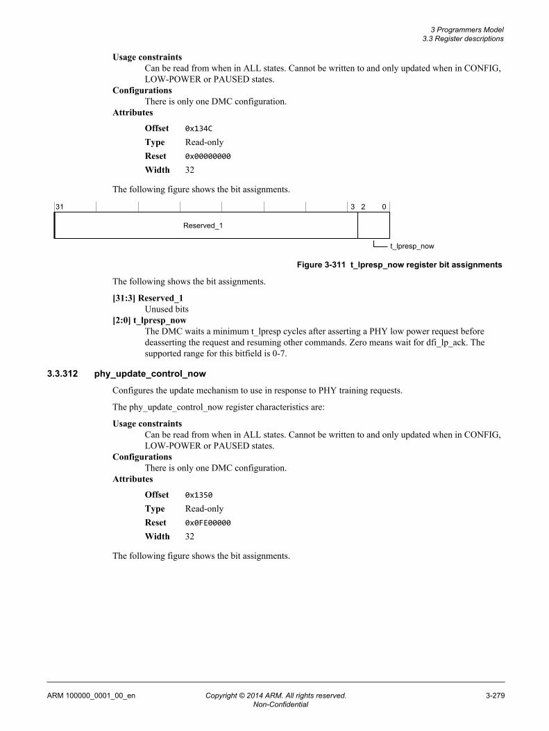
Usage constraintsCan be read from when in ALL states. Cannot be written to and only updated when in CONFIG,LOW-POWER or PAUSED states.
ConfigurationsThere is only one DMC configuration.
Attributes
Offset 0x134C
Type Read-onlyReset 0x00000000
Width 32
The following figure shows the bit assignments.
31 3 2 0
Reserved_1
t_lpresp_now
Figure 3-311 t_lpresp_now register bit assignments
The following shows the bit assignments.
[31:3] Reserved_1Unused bits
[2:0] t_lpresp_nowThe DMC waits a minimum t_lpresp cycles after asserting a PHY low power request beforedeasserting the request and resuming other commands. Zero means wait for dfi_lp_ack. Thesupported range for this bitfield is 0-7.
3.3.312 phy_update_control_now
Configures the update mechanism to use in response to PHY training requests.
The phy_update_control_now register characteristics are:
Usage constraintsCan be read from when in ALL states. Cannot be written to and only updated when in CONFIG,LOW-POWER or PAUSED states.
ConfigurationsThere is only one DMC configuration.
Attributes
Offset 0x1350
Type Read-onlyReset 0x0FE00000
Width 32
The following figure shows the bit assignments.
3 Programmers Model3.3 Register descriptions
ARM 100000_0001_00_en Copyright © 2014 ARM. All rights reserved. 3-279Non-Confidential

31 29 28 27 21 20 19 16 15 14 13 12 11 10 9 8 7 6 5 4 3 2 1 0
phyupd_type_01_nowReserved_1phyupd_type_00_now
Reserved_2phyupd_type_10_now
Reserved_4phyupd_type_11_nowReserved_3
t_ctrlupd_min_nowctrlupd_after_xsref_nowctrlupd_after_n_ref_now
phyupd_mode_nowReserved_5
Figure 3-312 phy_update_control_now register bit assignments
The following shows the bit assignments.
[31:29] Reserved_5Unused bits
[28] phyupd_mode_nowConfigures the DMC behavior in response to dfi_phyupd_req being asserted.
[27:21] t_ctrlupd_min_nowSets the number of cycles the DMC waits for acknowledgment of a cltrupd_req beforedeasserting the request and continuing normal operation. A value of 0x0 indicates the DMCmust always wait for an acknowledgment before proceeding. The supported range for thisbitfield is 0-127.
[20] ctrlupd_after_xsref_nowProgram to enable an automatic DMC-initiated PHY update request after exiting self-refresh
[19:16] ctrlupd_after_n_ref_nowProgram to enable an automatic DMC-initiated PHY update request after every nAUTOREFRESH commands. Zero disables the functionality. One is RESERVED
[15:14] Reserved_4Unused bits
[13:12] phyupd_type_11_nowProgram the required response to PHY update requests of type 11.
[11:10] Reserved_3Unused bits
[9:8] phyupd_type_10_nowProgram the required response to PHY update requests of type 10.
[7:6] Reserved_2Unused bits
[5:4] phyupd_type_01_nowProgram the required response to PHY update requests of type 01.
[3:2] Reserved_1Unused bits
[1:0] phyupd_type_00_nowProgram the required response to PHY update requests of type 00.
3.3.313 odt_timing_now
Configures the ODT on and off timing.
The odt_timing_now register characteristics are:
3 Programmers Model3.3 Register descriptions
ARM 100000_0001_00_en Copyright © 2014 ARM. All rights reserved. 3-280Non-Confidential

Usage constraintsCan be read from when in ALL states. Cannot be written to and only updated when in CONFIG,LOW-POWER or PAUSED states.
ConfigurationsThere is only one DMC configuration.
Attributes
Offset 0x1358
Type Read-onlyReset 0x06000600
Width 32
The following figure shows the bit assignments.
31 29 28 24 23 21 20 16 15 13 12 8 7 5 4 0
t_odt_off_wr_nowReserved_1t_odt_on_wr_now
Reserved_2t_odt_on_rd_now
Reserved_4t_odt_off_rd_nowReserved_3
Figure 3-313 odt_timing_now register bit assignments
The following shows the bit assignments.
[31:29] Reserved_4Unused bits
[28:24] t_odt_off_rd_nowTime from cs assertion to ODT being deasserted for read. The supported range for this bitfield is2-31.
[23:21] Reserved_3Unused bits
[20:16] t_odt_on_rd_nowTime from cs assertion to ODT being asserted for read. The supported range for this bitfield is0-29.
[15:13] Reserved_2Unused bits
[12:8] t_odt_off_wr_nowTime from cs assertion to ODT being deasserted for write. The supported range for this bitfieldis 2-31.
[7:5] Reserved_1Unused bits
[4:0] t_odt_on_wr_nowTime from cs assertion to ODT being asserted for write. The supported range for this bitfield is0-29.
3.3.314 odt_wr_control_31_00_now
Configures the ODT on and off settings for active and inactive ranks during writes.
The odt_wr_control_31_00_now register characteristics are:
3 Programmers Model3.3 Register descriptions
ARM 100000_0001_00_en Copyright © 2014 ARM. All rights reserved. 3-281Non-Confidential

Usage constraintsCan be read from when in ALL states. Cannot be written to and only updated when in CONFIG,LOW-POWER or PAUSED states.
ConfigurationsThere is only one DMC configuration.
Attributes
Offset 0x1360
Type Read-onlyReset 0x08040201
Width 32
The following figure shows the bit assignments.
31 24 23 16 15 8 7 0
odt_mask_wr_cs2_nowodt_mask_wr_cs1_nowodt_mask_wr_cs0_now
odt_mask_wr_cs3_now
Figure 3-314 odt_wr_control_31_00_now register bit assignments
The following shows the bit assignments.
[31:24] odt_mask_wr_cs3_nowDrives the dfi_odt[7:0] output signal during a write to DRAM rank 3. The supported range forthis bitfield is 0-255.
[23:16] odt_mask_wr_cs2_nowDrives the dfi_odt[7:0] output signal during a write to DRAM rank 2. The supported range forthis bitfield is 0-255.
[15:8] odt_mask_wr_cs1_nowDrives the dfi_odt[7:0] output signal during a write to DRAM rank 1. The supported range forthis bitfield is 0-255.
[7:0] odt_mask_wr_cs0_nowDrives the dfi_odt[7:0] output signal during a write to DRAM rank 0. The supported range forthis bitfield is 0-255.
3.3.315 odt_wr_control_63_32_now
Configures the ODT on and off settings for active and inactive ranks during writes.
The odt_wr_control_63_32_now register characteristics are:
Usage constraintsCan be read from when in ALL states. Cannot be written to and only updated when in CONFIG,LOW-POWER or PAUSED states.
ConfigurationsThere is only one DMC configuration.
Attributes
Offset 0x1364
Type Read-onlyReset 0x80402010
Width 32
The following figure shows the bit assignments.
3 Programmers Model3.3 Register descriptions
ARM 100000_0001_00_en Copyright © 2014 ARM. All rights reserved. 3-282Non-Confidential

31 24 23 16 15 8 7 0
odt_mask_wr_cs6_nowodt_mask_wr_cs5_nowodt_mask_wr_cs4_now
odt_mask_wr_cs7_now
Figure 3-315 odt_wr_control_63_32_now register bit assignments
The following shows the bit assignments.
[31:24] odt_mask_wr_cs7_nowDrives the dfi_odt[7:0] output signal during a write to DRAM rank 7. The supported range forthis bitfield is 0-255.
[23:16] odt_mask_wr_cs6_nowDrives the dfi_odt[7:0] output signal during a write to DRAM rank 6. The supported range forthis bitfield is 0-255.
[15:8] odt_mask_wr_cs5_nowDrives the dfi_odt[7:0] output signal during a write to DRAM rank 5. The supported range forthis bitfield is 0-255.
[7:0] odt_mask_wr_cs4_nowDrives the dfi_odt[7:0] output signal during a write to DRAM rank 4. The supported range forthis bitfield is 0-255.
3.3.316 odt_rd_control_31_00_now
Configures the ODT on and off settings for active and inactive ranks during reads.
The odt_rd_control_31_00_now register characteristics are:
Usage constraintsCan be read from when in ALL states. Cannot be written to and only updated when in CONFIG,LOW-POWER or PAUSED states.
ConfigurationsThere is only one DMC configuration.
Attributes
Offset 0x1368
Type Read-onlyReset 0x00000000
Width 32
The following figure shows the bit assignments.
31 24 23 16 15 8 7 0
odt_mask_rd_cs2_nowodt_mask_rd_cs1_nowodt_mask_rd_cs0_now
odt_mask_rd_cs3_now
Figure 3-316 odt_rd_control_31_00_now register bit assignments
The following shows the bit assignments.
[31:24] odt_mask_rd_cs3_nowDrives the dfi_odt[7:0] output signal during a read to DRAM rank 3. The supported range forthis bitfield is 0-255.
3 Programmers Model3.3 Register descriptions
ARM 100000_0001_00_en Copyright © 2014 ARM. All rights reserved. 3-283Non-Confidential

[23:16] odt_mask_rd_cs2_nowDrives the dfi_odt[7:0] output signal during a read to DRAM rank 2. The supported range forthis bitfield is 0-255.
[15:8] odt_mask_rd_cs1_nowDrives the dfi_odt[7:0] output signal during a read to DRAM rank 1. The supported range forthis bitfield is 0-255.
[7:0] odt_mask_rd_cs0_nowDrives the dfi_odt[7:0] output signal during a read to DRAM rank 0. The supported range forthis bitfield is 0-255.
3.3.317 odt_rd_control_63_32_now
Configures the ODT on and off settings for active and inactive ranks during reads.
The odt_rd_control_63_32_now register characteristics are:
Usage constraintsCan be read from when in ALL states. Cannot be written to and only updated when in CONFIG,LOW-POWER or PAUSED states.
ConfigurationsThere is only one DMC configuration.
Attributes
Offset 0x136C
Type Read-onlyReset 0x00000000
Width 32
The following figure shows the bit assignments.
31 24 23 16 15 8 7 0
odt_mask_rd_cs6_nowodt_mask_rd_cs5_nowodt_mask_rd_cs4_now
odt_mask_rd_cs7_now
Figure 3-317 odt_rd_control_63_32_now register bit assignments
The following shows the bit assignments.
[31:24] odt_mask_rd_cs7_nowDrives the dfi_odt[7:0] output signal during a read to DRAM rank 7. The supported range forthis bitfield is 0-255.
[23:16] odt_mask_rd_cs6_nowDrives the dfi_odt[7:0] output signal during a read to DRAM rank 6. The supported range forthis bitfield is 0-255.
[15:8] odt_mask_rd_cs5_nowDrives the dfi_odt[7:0] output signal during a read to DRAM rank 5. The supported range forthis bitfield is 0-255.
[7:0] odt_mask_rd_cs4_nowDrives the dfi_odt[7:0] output signal during a read to DRAM rank 4. The supported range forthis bitfield is 0-255.
3.3.318 dq_map_control_15_00_now
Controls the DQ mapping compensation applied for CRC calculation. For each nibble of the DQ bus, theDIMM SPD defines a DQ Map Index to define the bit connectivity to each rank. Program the DQ Map
3 Programmers Model3.3 Register descriptions
ARM 100000_0001_00_en Copyright © 2014 ARM. All rights reserved. 3-284Non-Confidential

Index retrieved from the SPD for each nibble into the corresponding register in the DMC for correctCRC operation.
The dq_map_control_15_00_now register characteristics are:
Usage constraintsCan be read from when in ALL states. Cannot be written to and only updated when in CONFIG,LOW-POWER or PAUSED states.
ConfigurationsThere is only one DMC configuration.
Attributes
Offset 0x1380
Type Read-onlyReset 0x00000000
Width 32
The following figure shows the bit assignments.
31 30 29 24 23 22 21 16 15 14 13 8 7 6 5 0
dq_map_7_4_nowReserved_1dq_map_3_0_now
Reserved_2dq_map_11_8_now
Reserved_4dq_map_15_12_nowReserved_3
Figure 3-318 dq_map_control_15_00_now register bit assignments
The following shows the bit assignments.
[31:30] Reserved_4Unused bits
[29:24] dq_map_15_12_nowControls DQ mapping for bits [15:12] of the DQ bus.
[23:22] Reserved_3Unused bits
[21:16] dq_map_11_8_nowControls DQ mapping for bits [11:8] of the DQ bus.
[15:14] Reserved_2Unused bits
[13:8] dq_map_7_4_nowControls DQ mapping for bits [7:4] of the DQ bus.
[7:6] Reserved_1Unused bits
[5:0] dq_map_3_0_nowControls DQ mapping for bits [3:0] of the DQ bus.
3.3.319 dq_map_control_31_16_now
Controls the DQ mapping compensation applied for CRC calculation. For each nibble of the DQ bus, theDIMM SPD defines a DQ Map Index to define the bit connectivity to each rank. Program the DQ MapIndex retrieved from the SPD for each nibble into the corresponding register in the DMC for correctCRC operation.
The dq_map_control_31_16_now register characteristics are:
3 Programmers Model3.3 Register descriptions
ARM 100000_0001_00_en Copyright © 2014 ARM. All rights reserved. 3-285Non-Confidential
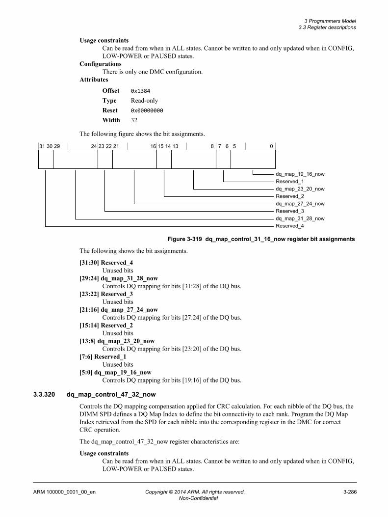
Usage constraintsCan be read from when in ALL states. Cannot be written to and only updated when in CONFIG,LOW-POWER or PAUSED states.
ConfigurationsThere is only one DMC configuration.
Attributes
Offset 0x1384
Type Read-onlyReset 0x00000000
Width 32
The following figure shows the bit assignments.
31 30 29 24 23 22 21 16 15 14 13 8 7 6 5 0
dq_map_23_20_nowReserved_1dq_map_19_16_now
Reserved_2dq_map_27_24_now
Reserved_4dq_map_31_28_nowReserved_3
Figure 3-319 dq_map_control_31_16_now register bit assignments
The following shows the bit assignments.
[31:30] Reserved_4Unused bits
[29:24] dq_map_31_28_nowControls DQ mapping for bits [31:28] of the DQ bus.
[23:22] Reserved_3Unused bits
[21:16] dq_map_27_24_nowControls DQ mapping for bits [27:24] of the DQ bus.
[15:14] Reserved_2Unused bits
[13:8] dq_map_23_20_nowControls DQ mapping for bits [23:20] of the DQ bus.
[7:6] Reserved_1Unused bits
[5:0] dq_map_19_16_nowControls DQ mapping for bits [19:16] of the DQ bus.
3.3.320 dq_map_control_47_32_now
Controls the DQ mapping compensation applied for CRC calculation. For each nibble of the DQ bus, theDIMM SPD defines a DQ Map Index to define the bit connectivity to each rank. Program the DQ MapIndex retrieved from the SPD for each nibble into the corresponding register in the DMC for correctCRC operation.
The dq_map_control_47_32_now register characteristics are:
Usage constraintsCan be read from when in ALL states. Cannot be written to and only updated when in CONFIG,LOW-POWER or PAUSED states.
3 Programmers Model3.3 Register descriptions
ARM 100000_0001_00_en Copyright © 2014 ARM. All rights reserved. 3-286Non-Confidential

ConfigurationsThere is only one DMC configuration.
Attributes
Offset 0x1388
Type Read-onlyReset 0x00000000
Width 32
The following figure shows the bit assignments.
31 30 29 24 23 22 21 16 15 14 13 8 7 6 5 0
dq_map_39_36_nowReserved_1dq_map_35_32_now
Reserved_2dq_map_43_40_now
Reserved_4dq_map_47_44_nowReserved_3
Figure 3-320 dq_map_control_47_32_now register bit assignments
The following shows the bit assignments.
[31:30] Reserved_4Unused bits
[29:24] dq_map_47_44_nowControls DQ mapping for bits [47:44] of the DQ bus.
[23:22] Reserved_3Unused bits
[21:16] dq_map_43_40_nowControls DQ mapping for bits [43:40] of the DQ bus.
[15:14] Reserved_2Unused bits
[13:8] dq_map_39_36_nowControls DQ mapping for bits [39:36] of the DQ bus.
[7:6] Reserved_1Unused bits
[5:0] dq_map_35_32_nowControls DQ mapping for bits [35:32] of the DQ bus.
3.3.321 dq_map_control_63_48_now
Controls the DQ mapping compensation applied for CRC calculation. For each nibble of the DQ bus, theDIMM SPD defines a DQ Map Index to define the bit connectivity to each rank. Program the DQ MapIndex retrieved from the SPD for each nibble into the corresponding register in the DMC for correctCRC operation.
The dq_map_control_63_48_now register characteristics are:
Usage constraintsCan be read from when in ALL states. Cannot be written to and only updated when in CONFIG,LOW-POWER or PAUSED states.
ConfigurationsThere is only one DMC configuration.
Attributes
3 Programmers Model3.3 Register descriptions
ARM 100000_0001_00_en Copyright © 2014 ARM. All rights reserved. 3-287Non-Confidential

Offset 0x138C
Type Read-onlyReset 0x00000000
Width 32
The following figure shows the bit assignments.
31 30 29 24 23 22 21 16 15 14 13 8 7 6 5 0
dq_map_55_52_nowReserved_1dq_map_51_48_now
Reserved_2dq_map_59_56_now
Reserved_4dq_map_63_60_nowReserved_3
Figure 3-321 dq_map_control_63_48_now register bit assignments
The following shows the bit assignments.
[31:30] Reserved_4Unused bits
[29:24] dq_map_63_60_nowControls DQ mapping for bits [63:60] of the DQ bus.
[23:22] Reserved_3Unused bits
[21:16] dq_map_59_56_nowControls DQ mapping for bits [59:56] of the DQ bus.
[15:14] Reserved_2Unused bits
[13:8] dq_map_55_52_nowControls DQ mapping for bits [55:52] of the DQ bus.
[7:6] Reserved_1Unused bits
[5:0] dq_map_51_48_nowControls DQ mapping for bits [51:48] of the DQ bus.
3.3.322 dq_map_control_71_64_now
Controls the DQ mapping compensation applied for CRC calculation. For each nibble of the DQ bus, theDIMM SPD defines a DQ Map Index to define the bit connectivity to each rank. Program the DQ MapIndex retrieved from the SPD for DIMM Check Bits bus into this register in the DMC for correct CRCoperation.
The dq_map_control_71_64_now register characteristics are:
Usage constraintsCan be read from when in ALL states. Cannot be written to and only updated when in CONFIG,LOW-POWER or PAUSED states.
ConfigurationsThere is only one DMC configuration.
Attributes
Offset 0x1390
Type Read-onlyReset 0x00000000
3 Programmers Model3.3 Register descriptions
ARM 100000_0001_00_en Copyright © 2014 ARM. All rights reserved. 3-288Non-Confidential

Width 32
The following figure shows the bit assignments.
31 24 23 16 15 14 13 8 7 6 5 0
Reserved_3
dq_map_71_68_nowReserved_1dq_map_67_64_now
Reserved_2rank_dq_bit_swap_now
Figure 3-322 dq_map_control_71_64_now register bit assignments
The following shows the bit assignments.
[31:24] Reserved_3Unused bits
[23:16] rank_dq_bit_swap_nowEach bit determines if the DQ bus has bit swapping as per the DDR4 RDIMM DesignSpecification applied to the corresponding rank. Normally, this bit must be set high for oddphysical ranks.
[15:14] Reserved_2Unused bits
[13:8] dq_map_71_68_nowControls DQ mapping for bits [71:68] of the DQ bus. This corresponds to CB [7:4] on theDIMM.
[7:6] Reserved_1Unused bits
[5:0] dq_map_67_64_nowControls DQ mapping for bits [67:64] of the DQ bus. This corresponds to CB [3:0] on theDIMM.
3.3.323 user_config0_now
Drives the output user_config0 signal.
The user_config0_now register characteristics are:
Usage constraintsCan be read from when in ALL states. Cannot be written to and only updated when in ALLstates.
ConfigurationsThere is only one DMC configuration.
Attributes
Offset 0x1408
Type Read-onlyReset 0x00000000
Width 32
The following figure shows the bit assignments.
31 0
user_config0_now
Figure 3-323 user_config0_now register bit assignments
3 Programmers Model3.3 Register descriptions
ARM 100000_0001_00_en Copyright © 2014 ARM. All rights reserved. 3-289Non-Confidential

The following shows the bit assignments.
[31:0] user_config0_nowuser_config0_now bitfield.
3.3.324 user_config1_now
Drives the output user_config1 signal.
The user_config1_now register characteristics are:
Usage constraintsCan be read from when in ALL states. Cannot be written to and only updated when in ALLstates.
ConfigurationsThere is only one DMC configuration.
Attributes
Offset 0x140C
Type Read-onlyReset 0x00000000
Width 32
The following figure shows the bit assignments.
31 0
user_config1_now
Figure 3-324 user_config1_now register bit assignments
The following shows the bit assignments.
[31:0] user_config1_nowuser_config1_now bitfield.
3.3.325 periph_id_4
Peripheral ID register.
The periph_id_4 register characteristics are:
Usage constraintsCan be read from when in ALL states. Cannot be changed.
ConfigurationsThere is only one DMC configuration.
Attributes
Offset 0x1FD0
Type Read-onlyReset 0x00000014
Width 32
The following figure shows the bit assignments.
31 8 7 4 3 0
DES_2SIZEReserved_1
Figure 3-325 periph_id_4 register bit assignments
The following shows the bit assignments.
3 Programmers Model3.3 Register descriptions
ARM 100000_0001_00_en Copyright © 2014 ARM. All rights reserved. 3-290Non-Confidential

[31:8] Reserved_1Unused bits
[7:4] SIZE4KB Count
[3:0] DES_2JEP continuation
3.3.326 periph_id_0
Peripheral ID register.
The periph_id_0 register characteristics are:
Usage constraintsCan be read from when in ALL states. Cannot be changed.
ConfigurationsThere is only one DMC configuration.
Attributes
Offset 0x1FE0
Type Read-onlyReset 0x00000052
Width 32
The following figure shows the bit assignments.
31 8 7 0
PART_0Reserved_1
Figure 3-326 periph_id_0 register bit assignments
The following shows the bit assignments.
[31:8] Reserved_1Unused bits
[7:0] PART_0Part Number [7:0]
3.3.327 periph_id_1
Peripheral ID register.
The periph_id_1 register characteristics are:
Usage constraintsCan be read from when in ALL states. Cannot be changed.
ConfigurationsThere is only one DMC configuration.
Attributes
Offset 0x1FE4
Type Read-onlyReset 0x000000B4
Width 32
The following figure shows the bit assignments.
3 Programmers Model3.3 Register descriptions
ARM 100000_0001_00_en Copyright © 2014 ARM. All rights reserved. 3-291Non-Confidential

31 8 7 4 3 0
PART_1DES_0Reserved_1
Figure 3-327 periph_id_1 register bit assignments
The following shows the bit assignments.
[31:8] Reserved_1Unused bits
[7:4] DES_0JEP106 Identity code [3:0]
[3:0] PART_1Part Number [11:8]
3.3.328 periph_id_2
Peripheral ID register.
The periph_id_2 register characteristics are:
Usage constraintsCan be read from when in ALL states. Cannot be changed.
ConfigurationsThere is only one DMC configuration.
Attributes
Offset 0x1FE8
Type Read-onlyReset 0x0000001B
Width 32
The following figure shows the bit assignments.
31 8 7 4 3 2 0
DES_1Reserved_1
REVISIONJEDEC
Figure 3-328 periph_id_2 register bit assignments
The following shows the bit assignments.
[31:8] Reserved_1Unused bits
[7:4] REVISIONRevision
[3] JEDECJEDEC JEP106 Code Is Used
[2:0] DES_1JEP106 Identity code [6:4]
3.3.329 periph_id_3
Peripheral ID register.
The periph_id_3 register characteristics are:
Usage constraintsCan be read from when in ALL states. Cannot be changed.
3 Programmers Model3.3 Register descriptions
ARM 100000_0001_00_en Copyright © 2014 ARM. All rights reserved. 3-292Non-Confidential

ConfigurationsThere is only one DMC configuration.
Attributes
Offset 0x1FEC
Type Read-onlyReset 0x00000000
Width 32
The following figure shows the bit assignments.
31 8 7 0
CMODReserved_1
Figure 3-329 periph_id_3 register bit assignments
The following shows the bit assignments.
[31:8] Reserved_1Unused bits
[7:0] CMODCustomer modified number.
3.3.330 component_id_0
Component ID register.
The component_id_0 register characteristics are:
Usage constraintsCan be read from when in ALL states. Cannot be changed.
ConfigurationsThere is only one DMC configuration.
Attributes
Offset 0x1FF0
Type Read-onlyReset 0x0000000D
Width 32
The following figure shows the bit assignments.
31 8 7 0
PRMBL_0Reserved_1
Figure 3-330 component_id_0 register bit assignments
The following shows the bit assignments.
[31:8] Reserved_1Unused bits
[7:0] PRMBL_0Component ID
3.3.331 component_id_1
Component ID register.
The component_id_1 register characteristics are:
3 Programmers Model3.3 Register descriptions
ARM 100000_0001_00_en Copyright © 2014 ARM. All rights reserved. 3-293Non-Confidential

Usage constraintsCan be read from when in ALL states. Cannot be changed.
ConfigurationsThere is only one DMC configuration.
Attributes
Offset 0x1FF4
Type Read-onlyReset 0x000000F0
Width 32
The following figure shows the bit assignments.
31 8 7 4 3 0
CLASSReserved_1
PRMBL_1
Figure 3-331 component_id_1 register bit assignments
The following shows the bit assignments.
[31:8] Reserved_1Unused bits
[7:4] CLASSComponent ID
[3:0] PRMBL_1Component ID
3.3.332 component_id_2
Component ID register.
The component_id_2 register characteristics are:
Usage constraintsCan be read from when in ALL states. Cannot be changed.
ConfigurationsThere is only one DMC configuration.
Attributes
Offset 0x1FF8
Type Read-onlyReset 0x00000005
Width 32
The following figure shows the bit assignments.
31 8 7 0
PRMBL_2Reserved_1
Figure 3-332 component_id_2 register bit assignments
The following shows the bit assignments.
[31:8] Reserved_1Unused bits
[7:0] PRMBL_2Component ID
3 Programmers Model3.3 Register descriptions
ARM 100000_0001_00_en Copyright © 2014 ARM. All rights reserved. 3-294Non-Confidential

3.3.333 component_id_3
Component ID register.
The component_id_3 register characteristics are:
Usage constraintsCan be read from when in ALL states. Cannot be changed.
ConfigurationsThere is only one DMC configuration.
Attributes
Offset 0x1FFC
Type Read-onlyReset 0x000000B1
Width 32
The following figure shows the bit assignments.
31 8 7 0
PRMBL_3Reserved_1
Figure 3-333 component_id_3 register bit assignments
The following shows the bit assignments.
[31:8] Reserved_1Unused bits
[7:0] PRMBL_3Component ID
3 Programmers Model3.3 Register descriptions
ARM 100000_0001_00_en Copyright © 2014 ARM. All rights reserved. 3-295Non-Confidential
Appendix ASignal Descriptions
This appendix describes the DMC-520 signals.
It contains the following sections:• A.1 Signals list on page Appx-A-297.
ARM 100000_0001_00_en Copyright © 2014 ARM. All rights reserved. Appx-A-296Non-Confidential

A.1 Signals listDMC signals list that excludes bus interface signals. The bus interface signals are defined by their ownbus protocol standard.
The following table shows the Primary clock and reset signals list of the DMC.
Table A-1 DMC Primary clock and reset signals list
Signal Type Width Description
clk Input 1 Primary DMC clock
resetn Input 1 Primary DMC reset
The following table shows the APB clock and reset signals list of the DMC.
Table A-2 DMC APB clock and reset signals list
Signal Type Width Description
pclk Input 1 APB clock
presetn Input 1 APB reset
The following table shows the User I/O with APB access list of the DMC.
Table A-3 DMC User I/O with APB access list
Signal Type Width Description
user_status Input 32 User defined inputs
user_config0 Output 32 User defined outputs
user_config1 Output 32 User defined outputs
user_config2 Output 32 User defined outputs
user_config3 Output 32 User defined outputs
user_periph_id_3 Input 8 Tie-off value to set the value of CMOD in the periph_id_3 bitfield. This input is exclusive ORedwith the default register value.
The following table shows the Events list of the DMC.
Table A-4 DMC Events list
Signal Type Width Description
scrub_event_in0 Input 1 Scrub event 0 trigger.
scrub_event_in1 Input 1 Scrub event 1 trigger.
scrub_event_in2 Input 1 Scrub event 2 trigger.
scrub_event_in3 Input 1 Scrub event 3 trigger.
scrub_event_in4 Input 1 Scrub event 4 trigger.
scrub_event_in5 Input 1 Scrub event 5 trigger.
scrub_event_in6 Input 1 Scrub event 6 trigger.
A Signal DescriptionsA.1 Signals list
ARM 100000_0001_00_en Copyright © 2014 ARM. All rights reserved. Appx-A-297Non-Confidential

Table A-4 DMC Events list (continued)
Signal Type Width Description
scrub_event_in7 Input 1 Scrub event 7 trigger.
scrub_event_out0 Output 1 Scrub event 0 triggered.
scrub_event_out1 Output 1 Scrub event 1 triggered.
scrub_event_out2 Output 1 Scrub event 2 triggered.
scrub_event_out3 Output 1 Scrub event 3 triggered.
scrub_event_out4 Output 1 Scrub event 4 triggered.
scrub_event_out5 Output 1 Scrub event 5 triggered.
scrub_event_out6 Output 1 Scrub event 6 triggered.
scrub_event_out7 Output 1 Scrub event 7 triggered.
direct_cmd_event_in0 Input 1 Direct cmd event 0 trigger.
direct_cmd_event_in1 Input 1 Direct cmd event 1 trigger.
direct_cmd_event_in2 Input 1 Direct cmd event 2 trigger.
direct_cmd_event_in3 Input 1 Direct cmd event 3 trigger.
direct_cmd_event_out0 Output 1 Direct cmd event 0 triggered.
direct_cmd_event_out1 Output 1 Direct cmd event 1 triggered.
direct_cmd_event_out2 Output 1 Direct cmd event 2 triggered.
direct_cmd_event_out3 Output 1 Direct cmd event 3 triggered.
The following table shows the Scan Signals list of the DMC.
Table A-5 DMC Scan Signals list
Signal Type Width Description
dftse Input 1 DFT scan enable
dftclkcgen Input 1 DFT clk clock gate enable
dftclkdiv2cgen Input 1 DFT clkdiv2 clock gate enable
dftpclkcgen Input 1 DFT pclk clock gate enable
dftrstdisable Input 1 DFT reset synchronizer disable
dftramhold Input 1 DFT on-chip RAM hold
dftmcphold Input 1 DFT multi-cycle path hold
The following table shows the PMU Signals list of the DMC.
Table A-6 DMC PMU Signals list
Signal Type Width Description
ev_request_valid_valid Output 1 Indicates that ev_request_valid_payload is valid
ev_request_tzfail_valid Output 1 Indicates that ev_request_tzfail_payload is valid
ev_request_retry_valid Output 1 Indicates that ev_request_retry_payload is valid
A Signal DescriptionsA.1 Signals list
ARM 100000_0001_00_en Copyright © 2014 ARM. All rights reserved. Appx-A-298Non-Confidential

Table A-6 DMC PMU Signals list (continued)
Signal Type Width Description
ev_retry_grant_valid Output 1 Indicates that ev_retry_grant_payload is valid
ev_request_valid_payload Output 27 A request enters the DMC
ev_request_tzfail_payload Output 22 A request fails an address translation or TrustZonepermissions check
ev_request_retry_payload Output 25 A request is retried
ev_retry_grant_payload Output 15 Indicates that a P-credit has been granted.
ev_queue_fill_status_payload Output 8 Count of entries in the DMC
ev_queued_reads_payload Output 8 Count of read entries in the DMC
ev_queued_writes_payload Output 8 Count of write entries in the DMC
ev_enqueued_reads_payload Output 8 Count of read entries in the queue
ev_enqueued_writes_payload Output 8 Count of write entries in the queue
ev_arbitrated_reads_payload Output 8 Count of read entries in the arbitrated, without datastate
ev_arbitrated_writes_payload Output 8 Count of write entries in the arbitrated, not clean state
ev_read_backlog_payload Output 8 Count of read entries in the backlog queue
ev_enqueue_backlog_payload Output 8 Count of entries that are waiting to get enqueued
ev_hazard_resolution_backlog_payload Output 8 Count of entries that are ready to be merged
ev_queue_allocation_backlog_payload Output 8 Count of entries that in allocation backlog
ev_enqueue_valid Output 1 Indicates that ev_enqueue_payload is valid
ev_arbitrate_valid Output 1 Indicates that ev_arbitrate_payload is valid
ev_rank_targetted_valid Output RANKS_PER_CHANNEL A rank is targeted by an enqueued entry
ev_enqueue_payload Output 34 A request is enqueued in the arbitration queue
ev_arbitrate_payload Output 12 A request is arbitrated from the arbitration queue
ev_allocate_valid Output 1 Indicates that ev_allocate_payload is valid
ev_allocate_payload Output 22 Maps sysid to allocated tag ID on entry to the DCB
ev_request_hazard_valid Output 1 Indicates that ev_request_hazard_payload is valid
ev_request_hazard_payload Output 2 A request forms a data hazard on an existing entry
ev_request_partial_valid Output 1 A request is partial (not a complete burst)
ev_request_rmw_valid Output 1 A request requires a read-modify-write
ev_ram_err_detect_valid Output 9 Indicates that ev_ram_err_detect_payload is valid
ev_ram_err_detect_payload Output 42 See ram_ecc_errd_int description
ev_ram_err_correct_valid Output 9 Indicates that ev_ram_err_correct_payload is valid
ev_ram_err_correct_payload Output 42 See ram_ecc_errc_int description
ev_dram_err_detect_valid Output 1 Indicates that ev_dram_err_detect_payload is valid
ev_dram_err_detect_payload Output 35 See dram_ecc_errd_int description
A Signal DescriptionsA.1 Signals list
ARM 100000_0001_00_en Copyright © 2014 ARM. All rights reserved. Appx-A-299Non-Confidential
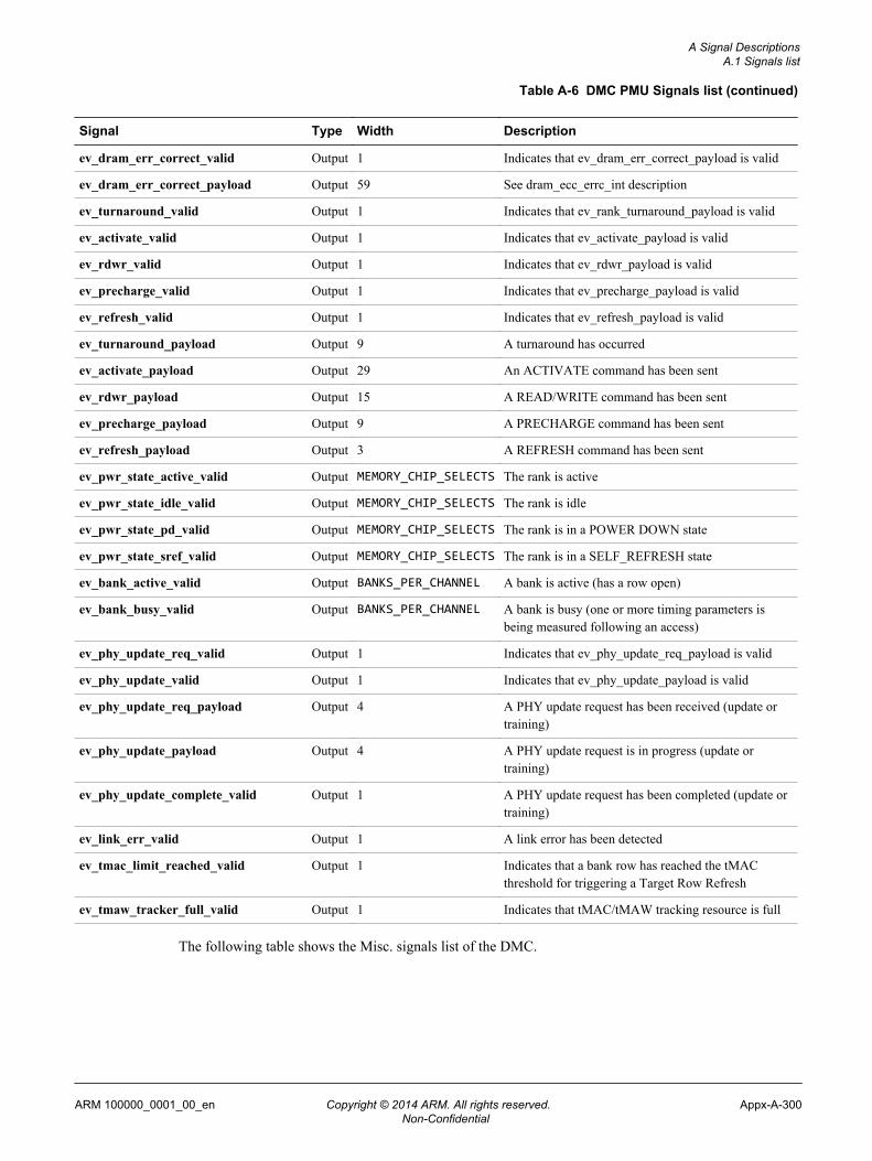
Table A-6 DMC PMU Signals list (continued)
Signal Type Width Description
ev_dram_err_correct_valid Output 1 Indicates that ev_dram_err_correct_payload is valid
ev_dram_err_correct_payload Output 59 See dram_ecc_errc_int description
ev_turnaround_valid Output 1 Indicates that ev_rank_turnaround_payload is valid
ev_activate_valid Output 1 Indicates that ev_activate_payload is valid
ev_rdwr_valid Output 1 Indicates that ev_rdwr_payload is valid
ev_precharge_valid Output 1 Indicates that ev_precharge_payload is valid
ev_refresh_valid Output 1 Indicates that ev_refresh_payload is valid
ev_turnaround_payload Output 9 A turnaround has occurred
ev_activate_payload Output 29 An ACTIVATE command has been sent
ev_rdwr_payload Output 15 A READ/WRITE command has been sent
ev_precharge_payload Output 9 A PRECHARGE command has been sent
ev_refresh_payload Output 3 A REFRESH command has been sent
ev_pwr_state_active_valid Output MEMORY_CHIP_SELECTS The rank is active
ev_pwr_state_idle_valid Output MEMORY_CHIP_SELECTS The rank is idle
ev_pwr_state_pd_valid Output MEMORY_CHIP_SELECTS The rank is in a POWER DOWN state
ev_pwr_state_sref_valid Output MEMORY_CHIP_SELECTS The rank is in a SELF_REFRESH state
ev_bank_active_valid Output BANKS_PER_CHANNEL A bank is active (has a row open)
ev_bank_busy_valid Output BANKS_PER_CHANNEL A bank is busy (one or more timing parameters isbeing measured following an access)
ev_phy_update_req_valid Output 1 Indicates that ev_phy_update_req_payload is valid
ev_phy_update_valid Output 1 Indicates that ev_phy_update_payload is valid
ev_phy_update_req_payload Output 4 A PHY update request has been received (update ortraining)
ev_phy_update_payload Output 4 A PHY update request is in progress (update ortraining)
ev_phy_update_complete_valid Output 1 A PHY update request has been completed (update ortraining)
ev_link_err_valid Output 1 A link error has been detected
ev_tmac_limit_reached_valid Output 1 Indicates that a bank row has reached the tMACthreshold for triggering a Target Row Refresh
ev_tmaw_tracker_full_valid Output 1 Indicates that tMAC/tMAW tracking resource is full
The following table shows the Misc. signals list of the DMC.
A Signal DescriptionsA.1 Signals list
ARM 100000_0001_00_en Copyright © 2014 ARM. All rights reserved. Appx-A-300Non-Confidential

Table A-7 DMC Misc. signals list
Signal Type Width Description
memory_type Output 3 An external output of the value of the memory_type register bitfield.
abort_req Input 1 An input to abort retries in the face of DFI link errors.
abort_ack Output 1 An output to acknowledge that the DMC has completed outstanding transactions as a result of anabort.
The following table shows the Tie-off signals list of the DMC.
Table A-8 DMC Tie-off signals list
Signal Type Width Description
t_rddata_en_diff_tie_off Input 6 Tie-off value for reset of register bitfield t_rddata_en_diff
t_phyrdcslat_tie_off Input 5 Tie-off value for reset of register bitfield t_phyrdcslat
t_phyrdlat_tie_off Input 6 Tie-off value for reset of register bitfield t_phyrdlat
t_phywrlat_diff_tie_off Input 5 Tie-off value for reset of register bitfield t_phywrlat_diff
t_phywrcslat_tie_off Input 5 Tie-off value for reset of register bitfield t_phywrcslat
t_phywrdata_tie_off Input 1 Tie-off value for reset of register bitfield t_phywrdata
refresh_dur_rdlvl_tie_off Input 1 Tie-off value for reset of register bitfield refresh_dur_rdlvl
t_rdlvl_en_tie_off Input 6 Tie-off value for reset of register bitfield t_rdlvl_en
t_rdlvl_rr_tie_off Input 10 Tie-off value for reset of register bitfield t_rdlvl_rr
refresh_dur_wrlvl_tie_off Input 1 Tie-off value for reset of register bitfield refresh_dur_wrlvl
t_wrlvl_en_tie_off Input 6 Tie-off value for reset of register bitfield t_wrlvl_en
t_wrlvl_ww_tie_off Input 10 Tie-off value for reset of register bitfield t_wrlvl_ww
t_lpresp_tie_off Input 3 Tie-off value for reset of register bitfield t_lpresp
user_config0_tie_off Input 32 Tie-off value for reset of register bitfield user_config0
user_config1_tie_off Input 32 Tie-off value for reset of register bitfield user_config1
user_config2_tie_off Input 32 Tie-off value for reset of register bitfield user_config2
user_config3_tie_off Input 32 Tie-off value for reset of register bitfield user_config3
The following table shows the Tie-off values for AMBA5 CHI list of the DMC.
Table A-9 DMC Tie-off values for AMBA5 CHI list
Signal Type Width Description
system_id Input SKY_RSP_FLIT_SRCID_WIDTHparmname> Tie-off value to set the physicalnode ID of the DMC
home_node_id Input (SKY_REQ_FLIT_SRCID_WIDTH*SYSTEM_REQUESTORS)parmname> Tie off value to specify theconcatenated physical node IDs ofup to 8 Home Nodes that arepermitted to access the DMC
The following table shows the DFI Interface bus list of the DMC.
A Signal DescriptionsA.1 Signals list
ARM 100000_0001_00_en Copyright © 2014 ARM. All rights reserved. Appx-A-301Non-Confidential

Table A-10 DMC DFI Interface list
Name Width Description
dfi_address 18 Address to DDR3 PHY
dfi_bank 3 Bank Address to PHY
dfi_ras_n 1 Row address strobe to PHY
dfi_cas_n 1 Column address strobe to PHY
dfi_we_n 1 Write enable to PHY
dfi_cs_n MEMORY_CHIP_SELECTS Chip-select to PHY
dfi_act_n 1 Activate to PHY
dfi_bg 2 Bank group address to PHY
dfi_cid 3 Chip ID to PHY
dfi_cke MEMORY_CHIP_SELECTS Clock enable to PHY
dfi_odt MEMORY_CHIP_SELECTS On Die Termination to PHY
dfi_reset_n MEMORY_CHIP_SELECTS Reset to PHY
dfi_parity_in 1 Command parity to PHY
dfi_wrdata_en (DMC_DATA_BYTES +DMC_ECC_BYTES)
Write data enable PHY
dfi_wrdata (DMC_DATA_BITS +DMC_ECC_BITS)
Write data to PHY
dfi_wrdata_cs_n MEMORY_CHIP_SELECTS Write Data Path Chip-select to PHY
dfi_wrdata_mask (DMC_DATA_BYTES +DMC_ECC_BYTES)
Write data mask PHY
dfi_rddata_en (DMC_DATA_BYTES +DMC_ECC_BYTES)
Enable for read data
dfi_rddata (DMC_DATA_BITS +DMC_ECC_BITS)
Read data input from PHY
dfi_rddata_dbi_n (DMC_DATA_BYTES +DMC_ECC_BYTES) * 2
Read Data DBI. This signal is sent with dfi_rddata bus indicatingDBI functionality. If not used this signal must be tied to 'b1.
dfi_rddata_valid (DMC_DATA_BYTES +DMC_ECC_BYTES)
Indicates read data valid
dfi_rddata_cs_n MEMORY_CHIP_SELECTS Read Data Path Chip-select to PHY
dfi_ctrlupd_req 1 This signal is part of DFI 3.0, see JEDEC specification for moreinformation.
dfi_ctrlupd_ack 1 This signal is part of DFI 3.0, see JEDEC specification for moreinformation.
dfi_phyupd_req 1 DFI PHY-initiated update request
dfi_phyupd_ack 1 DFI PHY-initiated update acknowledge
dfi_phyupd_type 2 DFI PHY-initiated update type
A Signal DescriptionsA.1 Signals list
ARM 100000_0001_00_en Copyright © 2014 ARM. All rights reserved. Appx-A-302Non-Confidential

Table A-10 DMC DFI Interface list (continued)
Name Width Description
dfi_phy_crc_mode 1 Sends CRC data as part of the data burst. 'b0 = CRC codegeneration and validation performed in the MC. 'b1 = CRC codegeneration and validation performed in the PHY.
dfi_data_byte_disable (DMC_DATA_BYTES +DMC_ECC_BYTES)
This signal is part of DFI 3.0, see JEDEC specification for moreinformation.
dfi_dram_clk_disable MEMORY_CHIP_SELECTS DRAM clock disable to PHY
dfi_init_start 1 This signal is part of DFI 3.0, see JEDEC specification for moreinformation.
dfi_init_complete 1 Indicates PHY initialization complete
dfi_alert_n 1 This signal is part of DFI 3.0, see JEDEC specification for moreinformation.
dfi_err 1 This signal is part of DFI 3.0, see JEDEC specification for moreinformation.
dfi_err_info 4 This signal is part of DFI 3.0, see JEDEC specification for moreinformation.
dfi_phylvl_req_cs_n MEMORY_CHIP_SELECTS This signal is part of DFI 3.1, see JEDEC specification for moreinformation.
dfi_phylvl_ack_cs_n MEMORY_CHIP_SELECTS This signal is part of DFI 3.1, see JEDEC specification for moreinformation.
dfi_rdlvl_req 1 DFI read data eye training request
dfi_rdlvl_cs_n MEMORY_CHIP_SELECTS DFI read data eye training request target chip-select
dfi_rdlvl_periodic 1 DFI read data eye training request periodic
dfi_rdlvl_en 1 DFI read data eye training enable
dfi_rdlvl_resp 1 DFI read data eye training response
dfi_rdlvl_gate_req 1 DFI read gate training request
dfi_rdlvl_gate_cs_n MEMORY_CHIP_SELECTS DFI read gate training request target chip-select
dfi_rdlvl_gate_periodic 1 DFI read gate training request periodic
dfi_rdlvl_gate_en 1 DFI read gate training enable
dfi_rdlvl_gate_resp 1 DFI read gate training response
dfi_wrlvl_req 1 DFI write leveling training request
dfi_wrlvl_cs_n MEMORY_CHIP_SELECTS DFI write leveling training request target chip-select
dfi_wrlvl_periodic 1 DFI write leveling training request periodic
dfi_wrlvl_en 1 DFI write leveling training enable
dfi_wrlvl_strobe 1 DFI write leveling training strobe
dfi_wrlvl_resp 1 DFI write leveling training response
dfi_lvl_pattern 4 This signal is part of DFI 3.0, see JEDEC specification for moreinformation.
A Signal DescriptionsA.1 Signals list
ARM 100000_0001_00_en Copyright © 2014 ARM. All rights reserved. Appx-A-303Non-Confidential

Table A-10 DMC DFI Interface list (continued)
Name Width Description
dfi_lvl_periodic 1 This signal is part of DFI 3.0, see JEDEC specification for moreinformation.
dfi_lvl_cs_n MEMORY_CHIP_SELECTS This signal is part of DFI 3.0, see JEDEC specification for moreinformation.
dfi_ref_en 1 DFI refresh during training enable
dfi_lp_ctrl_req 1 DFI command low power request
dfi_lp_data_req 1 DFI data low power request
dfi_lp_wakeup 4 DFI command low power PHY wakeup allowance
dfi_lp_ack 1 DFI command low power acknowledge
The following table shows the Q-Channel Interface for DMC bus list of the DMC.
Table A-11 DMC Q-Channel Interface for DMC list
Name Width Description
qreqn 1 Request from the external clock controller to prepare to stop the clock
qacceptn 1 Positive acknowledgment after receiving QREQn assertion indicating that the DMC has completed preparation tostop the clocks and that the external clock controller can stop the clock
qdeny 1 Negative acknowledgment after receiving QREQn assertion indicating that the DMC has refused the request fromthe external clock controller to prepare to stop the clock
qactive 1 Indication that the DMC is active
The following table shows the Q-Channel Interface for APB interface bus list of the DMC.
Table A-12 DMC Q-Channel Interface for APB interface list
Name Width Description
qreqn_apb 1 Request from the external clock controller to prepare to stop the clock
qacceptn_apb 1 Positive acknowledgment after receiving QREQn assertion indicating that the APB interface has completedpreparation to stop the clocks and that the external clock controller can stop the clock
qdeny_apb 1 Negative acknowledgment after receiving QREQn assertion indicating that the APB interface has refused therequest from the external clock controller to prepare to stop the clock
qactive_apb 1 Indication that the APB interface is active
The following table shows the Clock Frequency Change Interface bus list of the DMC.
Table A-13 DMC Clock Frequency Change Interface list
Name Width Description
cc_frequency 5 Used to indicate new frequency as part of frequency change protocol
cc_freq_change_req 1 Signals to an external clock control that the clock frequency can be updated
cc_freq_change_ack 1 Signals to the DMC from an external clock control that the clock frequency has been updated
A Signal DescriptionsA.1 Signals list
ARM 100000_0001_00_en Copyright © 2014 ARM. All rights reserved. Appx-A-304Non-Confidential

The following table shows the Clock Frequency Change Interface bus list of the DMC.
Table A-14 DMC Clock Frequency Change Interface list
Name Width Description
dfi_frequency 5 Used to indicate new frequency as part of frequency change protocol
dfi_freq_change_req 1 Signals to an external clock control that the clock frequency can be updated
dfi_freq_change_ack 1 Signals to the DMC from an external clock control that the clock frequency has been updated
The following table shows the Memory BIST interface bus list of the DMC.
Table A-15 DMC Memory BIST interface list
Name Width Description
mbistresetn 1 MBIST reset. Active low.
mbistreq 1 MBIST request
mbistack 1 MBIST acknowledge
mbistwriteen 1 MBIST write enable
mbistreaden 1 MBIST read enable
mbistaddr 7 MBIST address
mbistarray 5 MBIST array selection
mbistindata 154 MBIST write data
mbistoutdata 154 MBIST read data
The following table shows the interrupt signal list of the DMC. All the signals are outputs from theDMC.
Table A-16 DMC interrupt list
Name Width Description
ram_ecc_errc_int 1 The DMC has detected a correctable error in an internal RAM
ram_ecc_errd_int 1 The DMC has detected an un-correctable error in an internal RAM
dram_ecc_errc_int 1 The DMC has detected a correctable error in a DRAM burst
dram_ecc_errd_int 1 The DMC has detected a data failure that could not be corrected in a DRAM burst operation
failed_access_int 1 The DMC has detected a system request that has failed a permissions check
failed_prog_int 1 The DMC has detected a programming request that is not permitted
link_err_int 1 The DRAM interface has suffered from a link failure and a recovery attempt has begun
temperature_event_int 1 The DMC has detected a temperature event signaled by the DRAM, either directly, or if atemperature delta has been observed through automated polling of the temperature sensor
arch_fsm_int 1 The DMC has detected a change in the architectural state
phy_request_int 1 The DMC has detected a PHY request
combined_int 1 A combined interrupt that is the logical OR of the other interrupts
ram_ecc_errc_oflow 1 The DMC has detected a correctable error in an internal RAM and a previously detectedassertion was not cleared
A Signal DescriptionsA.1 Signals list
ARM 100000_0001_00_en Copyright © 2014 ARM. All rights reserved. Appx-A-305Non-Confidential

Table A-16 DMC interrupt list (continued)
Name Width Description
ram_ecc_errd_oflow 1 The DMC has detected a un-correctable error in an internal RAM and a previously detectedassertion was not cleared
dram_ecc_errc_oflow 1 The DMC has detected a correctable error in a DRAM burst and a previously detected assertionwas not cleared
dram_ecc_errd_oflow 1 The DMC has detected a data failure that could not be corrected in a DRAM burst operation anda previously detected assertion was not cleared
failed_access_oflow 1 The DMC has detected a system request that has failed a permissions check and a previouslydetected assertion was not cleared
failed_prog_oflow 1 The DMC has detected a programming request that is not permitted and a previously detectedassertion was not cleared
link_err_oflow 1 The DRAM interface has suffered from a link failure and a recovery attempt has begun and apreviously detected assertion was not cleared
temperature_event_oflow 1 The DMC has detected a temperature event signaled by the DRAM, either directly, or if atemperature delta has been observed through automated polling of the temperature sensor and apreviously detected assertion was not cleared
arch_fsm_oflow 1 The DMC has detected a change in the architectural state and a previously detected assertion wasnot cleared
phy_request_oflow 1 The DMC has detected a PHY request and a previously detected assertion was not cleared
combined_oflow 1 A combined interrupt that is the logical OR of the other interrupt overflows
A Signal DescriptionsA.1 Signals list
ARM 100000_0001_00_en Copyright © 2014 ARM. All rights reserved. Appx-A-306Non-Confidential

Appendix BRevisions
This appendix describes the technical changes between released issues of this book.
It contains the following sections:• B.1 Revisions on page Appx-B-308.
ARM 100000_0001_00_en Copyright © 2014 ARM. All rights reserved. Appx-B-307Non-Confidential

B.1 RevisionsThis appendix describes the technical changes between released issues of this book.
Table B-1 Revision 0000 issue 00
Change Location Affects
First release - -
Table B-2 Differences between revision 0000 issue 00 and revision 0001 issue 00
Change Location Affects
Programmable registers updated Chapter 3 Programmers Model on page 3-31 All revisions
DIMM supported list updated. 2.4 Constraints and limitations of use on page 2-29 All revisions
B RevisionsB.1 Revisions
ARM 100000_0001_00_en Copyright © 2014 ARM. All rights reserved. Appx-B-308Non-Confidential