technical reference manual - arm information...
TRANSCRIPT
ARM® Cortex®-M3 ProcessorRevision: r2p1
Technical Reference Manual
Copyright © 2005-2008, 2010, 2015 ARM. All rights reserved.ARM 100165_0201_00_en

ARM® Cortex®-M3 ProcessorTechnical Reference ManualCopyright © 2005-2008, 2010, 2015 ARM. All rights reserved.
Release Information
Document History
Issue Date Confidentiality Change
A 15 December 2005 Confidential First Release
B 13 January 2006 Non-Confidential Confidentiality status amended
C 10 May 2006 Non-Confidential First Release for r1p0
D 27 September 2006 Non-Confidential First Release for r1p1
E 13 June 2007 Non-Confidential Minor update with no technical changes
F 11 April 2008 Confidential Limited release for SC300 r0p0
G 26 June 2008 Non-Confidential First Release for r2p0
H 26 February 2010 Non-Confidential Second Release for r2p0
I 07 July 2010 Non-Confidential First Release for r2p1
0201-00 24 February 2015 Non-Confidential Document source updated to comply with DITA standards.Document number changed to 100165. DITA-XML.
Non-Confidential Proprietary Notice
This document is protected by copyright and other related rights and the practice or implementation of the information contained inthis document may be protected by one or more patents or pending patent applications. No part of this document may bereproduced in any form by any means without the express prior written permission of ARM. No license, express or implied, byestoppel or otherwise to any intellectual property rights is granted by this document unless specifically stated.
Your access to the information in this document is conditional upon your acceptance that you will not use or permit others to usethe information for the purposes of determining whether implementations infringe any third party patents.
THIS DOCUMENT IS PROVIDED “AS IS”. ARM PROVIDES NO REPRESENTATIONS AND NO WARRANTIES,EXPRESS, IMPLIED OR STATUTORY, INCLUDING, WITHOUT LIMITATION, THE IMPLIED WARRANTIES OFMERCHANTABILITY, SATISFACTORY QUALITY, NON-INFRINGEMENT OR FITNESS FOR A PARTICULARPURPOSE WITH RESPECT TO THE DOCUMENT. For the avoidance of doubt, ARM makes no representation with respect to,and has undertaken no analysis to identify or understand the scope and content of, third party patents, copyrights, trade secrets, orother rights.
This document may include technical inaccuracies or typographical errors.
TO THE EXTENT NOT PROHIBITED BY LAW, IN NO EVENT WILL ARM BE LIABLE FOR ANY DAMAGES,INCLUDING WITHOUT LIMITATION ANY DIRECT, INDIRECT, SPECIAL, INCIDENTAL, PUNITIVE, ORCONSEQUENTIAL DAMAGES, HOWEVER CAUSED AND REGARDLESS OF THE THEORY OF LIABILITY, ARISINGOUT OF ANY USE OF THIS DOCUMENT, EVEN IF ARM HAS BEEN ADVISED OF THE POSSIBILITY OF SUCHDAMAGES.
This document consists solely of commercial items. You shall be responsible for ensuring that any use, duplication or disclosure ofthis document complies fully with any relevant export laws and regulations to assure that this document or any portion thereof isnot exported, directly or indirectly, in violation of such export laws. Use of the word “partner” in reference to ARM’s customers isnot intended to create or refer to any partnership relationship with any other company. ARM may make changes to this document atany time and without notice.
If any of the provisions contained in these terms conflict with any of the provisions of any signed written agreement covering thisdocument with ARM, then the signed written agreement prevails over and supersedes the conflicting provisions of these terms.This document may be translated into other languages for convenience, and you agree that if there is any conflict between theEnglish version of this document and any translation, the terms of the English version of the Agreement shall prevail.
ARM® Cortex®-M3 Processor
ARM 100165_0201_00_en Copyright © 2005-2008, 2010, 2015 ARM. All rights reserved. 2Non-Confidential

Words and logos marked with ® or ™ are registered trademarks or trademarks of ARM Limited or its affiliates in the EU and/orelsewhere. All rights reserved. Other brands and names mentioned in this document may be the trademarks of their respectiveowners. Please follow ARM’s trademark usage guidelines at http://www.arm.com/about/trademark-usage-guidelines.php
Copyright © [2005-2008, 2010, 2015], ARM Limited or its affiliates. All rights reserved.
ARM Limited. Company 02557590 registered in England.
110 Fulbourn Road, Cambridge, England CB1 9NJ.
LES-PRE-20349
Confidentiality Status
This document is Non-Confidential. The right to use, copy and disclose this document may be subject to license restrictions inaccordance with the terms of the agreement entered into by ARM and the party that ARM delivered this document to.
Unrestricted Access is an ARM internal classification.
Product Status
The information in this document is Final, that is for a developed product.
Web Address
http://www.arm.com
ARM® Cortex®-M3 Processor
ARM 100165_0201_00_en Copyright © 2005-2008, 2010, 2015 ARM. All rights reserved. 3Non-Confidential

ContentsARM® Cortex®-M3 Processor Technical ReferenceManual
PrefaceAbout this book ...................................................... ...................................................... 7Feedback .................................................................................................................... 10
Chapter 1 Introduction1.1 About the processor ................................................ ................................................ 1-121.2 Processor features list .............................................. .............................................. 1-131.3 External interfaces ................................................. ................................................. 1-141.4 Optional implementation components .................................. .................................. 1-151.5 Product documentation ............................................................................................ 1-161.6 Product revisions .................................................. .................................................. 1-19
Chapter 2 Functional Description2.1 About the functions .................................................................................................. 2-222.2 Processor features list .............................................. .............................................. 2-232.3 Interfaces ........................................................ ........................................................ 2-25
Chapter 3 Programmers Model3.1 About the programmers’ model ....................................... ....................................... 3-293.2 Modes of operation and execution ..................................... ..................................... 3-303.3 Instruction set summary ............................................. ............................................. 3-313.4 Processor memory model ........................................................................................ 3-37
ARM 100165_0201_00_en Copyright © 2005-2008, 2010, 2015 ARM. All rights reserved. 4Non-Confidential

3.5 Write buffer .............................................................................................................. 3-403.6 Exclusive monitor .................................................. .................................................. 3-413.7 Bit-banding ....................................................... ....................................................... 3-423.8 Processor core register summary ............................................................................ 3-443.9 Exceptions ....................................................... ....................................................... 3-46
Chapter 4 System Control4.1 System control registers .......................................................................................... 4-494.2 Auxiliary Control Register, ACTLR ..................................... ..................................... 4-514.3 CPUID Base Register, CPUID ........................................ ........................................ 4-524.4 Auxiliary Fault Status Register, AFSR .................................. .................................. 4-53
Chapter 5 Memory Protection Unit5.1 About the MPU .................................................... .................................................... 5-555.2 MPU functional description ...................................................................................... 5-565.3 MPU programmers model table ....................................... ....................................... 5-57
Chapter 6 Nested Vectored Interrupt Controller6.1 NVIC functional description .......................................... .......................................... 6-596.2 NVIC programmers’ model ...................................................................................... 6-60
Chapter 7 Debug7.1 Debug configuration ................................................ ................................................ 7-637.2 AHB-AP debug access port .......................................... .......................................... 7-677.3 Flash Patch and Breakpoint Unit (FPB) ................................. ................................. 7-70
Chapter 8 Data Watchpoint and Trace Unit8.1 DWT functional description ...................................................................................... 8-738.2 DWT Programmers’ model ...................................................................................... 8-74
Chapter 9 Instrumentation Trace Macrocell Unit9.1 ITM functional description ........................................................................................ 9-779.2 ITM programmers’ model ............................................ ............................................ 9-789.3 ITM Trace Privilege Register, ITM_TPR .................................................................. 9-79
Chapter 10 Embedded Trace Macrocell10.1 About the ETM ................................................... ................................................... 10-8110.2 ETM functional description .......................................... .......................................... 10-8210.3 ETM Programmers model .......................................... .......................................... 10-88
Chapter 11 Trace Port Interface Unit11.1 About the TPIU .................................................................................................... 11-10411.2 TPIU functional description .................................................................................. 11-10511.3 TPIU programmers model ......................................... ......................................... 11-107
Appendix A RevisionsA.1 Revisions .................................................. .................................................. Appx-A-117
ARM 100165_0201_00_en Copyright © 2005-2008, 2010, 2015 ARM. All rights reserved. 5Non-Confidential

Preface
This preface introduces the ARM® Cortex®-M3 Processor Technical Reference Manual.
It contains the following:• About this book on page 7.• Feedback on page 10.
ARM 100165_0201_00_en Copyright © 2005-2008, 2010, 2015 ARM. All rights reserved. 6Non-Confidential

About this bookThis book contains documentation for the Cortex-M3 processor, describing the programmers model,instructions, registers, memory map, cache and debug support. Components include ETM, MPU, NVIC,FPB, DWT, ITM, AHB, and TPIU.
Product revision status
The rmpn identifier indicates the revision status of the product described in this book, for example, r1p2,where:
rm Identifies the major revision of the product, for example, r1.pn Identifies the minor revision or modification status of the product, for example, p2.
Intended audience
This manual is written to help system designers, system integrators, verification engineers, and softwareprogrammers who are implementing a System-on-Chip (SoC) device based on the Cortex®-M3 processor.
Using this book
This book is organized into the following chapters:
Chapter 1 IntroductionThis chapter introduces the processor and processor instruction set.
Chapter 2 Functional DescriptionThis chapter introduces the processor and its external interfaces.
Chapter 3 Programmers ModelThis chapter describes the processor programmers model.
Chapter 4 System ControlThis chapter provides a summary of the system control registers whose implementation is specificto the Cortex-M3 processor.
Chapter 5 Memory Protection UnitThis chapter describes the processor Memory Protection Unit (MPU).
Chapter 6 Nested Vectored Interrupt ControllerThis chapter describes the Nested Vectored Interrupt Controller (NVIC). The NVIC providesconfigurable interrupt handling abilities to the processor, facilitates low- latency exception andinterrupt handling, and controls power management.
Chapter 7 DebugThis chapter describes how to debug and test software running on the processor.
Chapter 8 Data Watchpoint and Trace UnitThis chapter describes the Data Watchpoint and Trace (DWT) unit.
Chapter 9 Instrumentation Trace Macrocell UnitThis chapter describes the Instrumentation Trace Macrocell (ITM) unit.
Chapter 10 Embedded Trace MacrocellThis chapter describes the Embedded Trace Macrocell (ETM).
Chapter 11 Trace Port Interface UnitThis chapter describes the Trace Port Interface Unit (TPIU) specific to this processor.
Appendix A RevisionsThe technical changes between released issues of this book.
Preface About this book
ARM 100165_0201_00_en Copyright © 2005-2008, 2010, 2015 ARM. All rights reserved. 7Non-Confidential
Glossary
The ARM Glossary is a list of terms used in ARM documentation, together with definitions for thoseterms. The ARM Glossary does not contain terms that are industry standard unless the ARM meaningdiffers from the generally accepted meaning.
See the ARM Glossary for more information.
Typographic conventions
italicIntroduces special terminology, denotes cross-references, and citations.
boldHighlights interface elements, such as menu names. Denotes signal names. Also used for termsin descriptive lists, where appropriate.
monospaceDenotes text that you can enter at the keyboard, such as commands, file and program names,and source code.
monospaceDenotes a permitted abbreviation for a command or option. You can enter the underlined textinstead of the full command or option name.
monospace italicDenotes arguments to monospace text where the argument is to be replaced by a specific value.
monospace boldDenotes language keywords when used outside example code.
<and>Encloses replaceable terms for assembler syntax where they appear in code or code fragments.For example:
MRC p15, 0 <Rd>, <CRn>, <CRm>, <Opcode_2>
SMALL CAPITALS
Used in body text for a few terms that have specific technical meanings, that are defined in theARM glossary. For example, IMPLEMENTATION DEFINED, IMPLEMENTATION SPECIFIC, UNKNOWN, andUNPREDICTABLE.
Timing diagrams
The following figure explains the components used in timing diagrams. Variations, when they occur,have clear labels. You must not assume any timing information that is not explicit in the diagrams.
Shaded bus and signal areas are undefined, so the bus or signal can assume any value within the shadedarea at that time. The actual level is unimportant and does not affect normal operation.
Clock
HIGH to LOW
Transient
HIGH/LOW to HIGH
Bus stable
Bus to high impedance
Bus change
High impedance to stable bus
Figure 1 Key to timing diagram conventions
Signals
The signal conventions are:
Preface About this book
ARM 100165_0201_00_en Copyright © 2005-2008, 2010, 2015 ARM. All rights reserved. 8Non-Confidential

Signal levelThe level of an asserted signal depends on whether the signal is active-HIGH or active-LOW.Asserted means:• HIGH for active-HIGH signals.• LOW for active-LOW signals.
Lower-case nAt the start or end of a signal name denotes an active-LOW signal.
Additional reading
This book contains information that is specific to this product. See the following documents for otherrelevant information.
ARM publications• ARMv7-M Architecture Reference Manual (ARM DDI 0403).• ARM® Cortex-M3 Integration and Implementation Manual (ARM DII 0240).• ARM AMBA® 3 AHB-Lite Protocol (v1.0) (ARM IHI 0033).• ARM AMBA 3 APB Protocol Specification (ARM IHI 0024).• AMBA 3 ATB Protocol Specification (ARM IHI 0032).• ARM CoreSight™ Components Technical Reference Manual (ARM DDI 0314).• ARM Debug Interface v5 Architecture Specification (ARM IHI 0031).• ARM Embedded Trace Macrocell Architecture Specification (ARM IHI 0014).
Other publicationsThis section lists relevant documents published by third parties:• IEEE Standard Test Access Port and Boundary-Scan Architecture 1149.1-2001 (JTAG).
Preface About this book
ARM 100165_0201_00_en Copyright © 2005-2008, 2010, 2015 ARM. All rights reserved. 9Non-Confidential

Feedback
Feedback on this product
If you have any comments or suggestions about this product, contact your supplier and give:• The product name.• The product revision or version.• An explanation with as much information as you can provide. Include symptoms and diagnostic
procedures if appropriate.
Feedback on content
If you have comments on content then send an e-mail to [email protected]. Give:• The title.• The number ARM 100165_0201_00_en.• The page number(s) to which your comments refer.• A concise explanation of your comments.
ARM also welcomes general suggestions for additions and improvements.
Note
ARM tests the PDF only in Adobe Acrobat and Acrobat Reader, and cannot guarantee the quality of therepresented document when used with any other PDF reader.
Preface Feedback
ARM 100165_0201_00_en Copyright © 2005-2008, 2010, 2015 ARM. All rights reserved. 10Non-Confidential

Chapter 1Introduction
This chapter introduces the processor and processor instruction set.
It contains the following sections:• 1.1 About the processor on page 1-12.• 1.2 Processor features list on page 1-13.• 1.3 External interfaces on page 1-14.• 1.4 Optional implementation components on page 1-15.• 1.5 Product documentation on page 1-16.• 1.6 Product revisions on page 1-19.
ARM 100165_0201_00_en Copyright © 2005-2008, 2010, 2015 ARM. All rights reserved. 1-11Non-Confidential

1.1 About the processorThe Cortex-M3 is a low-power processor that features low gate count, low interrupt latency, and low-cost debug. It is intended for deeply embedded applications that require optimal interrupt responsefeatures.
1 Introduction1.1 About the processor
ARM 100165_0201_00_en Copyright © 2005-2008, 2010, 2015 ARM. All rights reserved. 1-12Non-Confidential

1.2 Processor features listThe processor includes a core, a Nested Vectored Interrupt Controller (NVIC), high-performance businterfaces, and other features.
The processor incorporates the following features:• A processor core.• A Nested Vectored Interrupt Controller (NVIC) closely integrated with the processor core to achieve
low latency interrupt processing.• Multiple high-performance bus interfaces.• A low-cost debug solution with the optional ability to:
— Implement breakpoints and code patches.— Implement watchpoints, tracing, and system profiling.— Support printf() style debugging.— Bridge to a Trace Port Analyzer (TPA).
• An optional Memory Protection Unit (MPU).
1 Introduction1.2 Processor features list
ARM 100165_0201_00_en Copyright © 2005-2008, 2010, 2015 ARM. All rights reserved. 1-13Non-Confidential
1.3 External interfacesThe processor incorporates three external bus interfaces, an ETM interface that allows the connection ofan Embedded Trace Macrocell, an AHB Trace Macrocell interface that enables simple connection of anETM to the processor, and an Advanced High-performance Bus Access Port (AHB-AP) interface fordebug accesses.
The processor incorporates the following external interfaces:• Multiple memory and device bus interfaces.• ETM interface.• Trace port interface.• Debug port interface.
1 Introduction1.3 External interfaces
ARM 100165_0201_00_en Copyright © 2005-2008, 2010, 2015 ARM. All rights reserved. 1-14Non-Confidential
1.4 Optional implementation componentsYou can configure your processor implementation to include optional components. For example, aMemory Protection Unit (MPU), Flash Patch and Breakpoint (FPB), and Data Watchpoint and TraceUnit (DWT).
The full list of Cortex-M3 optional implementation components is:• Memory Protection Unit (MPU).• Flash Patch and Breakpoint (FPB).• Data Watchpoint and Trace Unit (DWT).• Instrumentation Trace Macrocell Unit (ITM).• Embedded Trace Macrocell (ETM).• Advanced High-performance Bus Access Port (AHB-AP).• AHB Trace Macrocell interface (HTM interface).• Trace Port Interface Unit (TPIU).• Wake-up Interrupt Controller (WIC).• Debug Port Debug Port AHB-AP interface.• Constant AHB control.
Note
You can only configure trace functionality in the following combinations:• No trace functionality.• ITM and DWT.• ITM, DWT, and ETM.• ITM, DWT, ETM, and HTM.
You can configure the debug features provided in the DWT independently.
1 Introduction1.4 Optional implementation components
ARM 100165_0201_00_en Copyright © 2005-2008, 2010, 2015 ARM. All rights reserved. 1-15Non-Confidential

1.5 Product documentationThe information supplied with this product includes a Technical Reference Manual, an Integration andImplementation manual, together with design flow, architecture, and protocol information.
This section contains the following subsections:• 1.5.1 Reference manuals on page 1-16.• 1.5.2 Design Flow on page 1-17.• 1.5.3 Architecture and protocol information on page 1-18.
1.5.1 Reference manuals
This product is supplied with a complete set of reference manuals that describe processor functionality,build configuration options, and reference material that ARM partners might want to include in their ownprocessor user guides.
Technical Reference ManualThe Technical Reference Manual (TRM) describes the functionality and the effects of functionaloptions on the behavior of the Cortex-M3 processor. It is required at all stages of the designflow. Some behavior described in the TRM might not be relevant because of the way that theCortex-M3 processor is implemented and integrated. If you are programming the Cortex-M3processor then contact:• The implementer to determine:
— The build configuration of the implementation.— What integration, if any, was performed before implementing the processor.
• The integrator to determine the pin configuration of the SoC that you are using.
Integration and Implementation ManualThe Integration and Implementation Manual (IIM) describes:• The available build configuration options and related issues in selecting them.• How to configure the Register Transfer Level (RTL) with the build configuration options.• How to integrate the processor into a SoC. This includes a description of the integration kit
and describes the pins that the integrator must tie off to configure the macrocell for therequired integration.
• How to implement the processor into your design. This includes floorplanning guidelines,Design for Test (DFT) information, and how to perform netlist dynamic verification on theprocessor.
• The processes to sign off the integration and implementation of the design.
The ARM product deliverables include reference scripts and information about using them toimplement your design.
Reference methodology documentation from your EDA tools vendor complements the IIM.
The IIM is a confidential book that is only available to licensees.
ETM-M4 Technical Reference ManualThe ETM-M4 TRM describes the functionality and behavior of the Cortex-M3 Embedded TraceMacrocell. It is required at all stages of the design flow. Typically the ETM-M4 is integratedwith the Cortex-M3 processor prior to implementation as a single macrocell.
1 Introduction1.5 Product documentation
ARM 100165_0201_00_en Copyright © 2005-2008, 2010, 2015 ARM. All rights reserved. 1-16Non-Confidential

Cortex-M3 User Guide Reference MaterialThis document provides reference material that ARM partners can configure and include in aUser Guide for an ARM Cortex-M3 processor. Typically:• Each chapter in this reference material might correspond to a section in the User Guide.• Each top-level section in this reference material might correspond to a chapter in the User
Guide.
However, you can organize this material in any way, subject to the conditions of the licenseagreement under which ARM supplied the material.
1.5.2 Design Flow
The design flow includes steps for implementation, integration, and programming. These processes mustbe completed before the processor is ready for operation.
The processor is delivered as synthesizable RTL. Before it can be used in a product, it must go throughthe following process:
ImplementationThe implementer configures the RTL and may synthesize it to produce a hard macrocell or maysynthesize the whole design after implementation.
IntegrationThe integrator connects the implemented design into a SoC. This includes connecting it to amemory system and peripherals.
ProgrammingThe system programmer develops the software required to configure and initialize the processor,and tests the required application software.
Each stage in the process can be performed by a different party. Implementation and integration choicesaffect the behavior and features of the processor.
For MCUs, often a single design team integrates the processor before synthesizing the complete design.Alternatively, the team can synthesize the processor on its own or partially integrated, to produce amacrocell that is then integrated, possibly by a separate team.
The operation of the final device depends on:
Build configurationThe implementer chooses the options that affect how the RTL source files are pre-processed.These options usually include or exclude logic that affects one or more of the area, maximumfrequency, and features of the resulting macrocell.
Configuration inputsThe integrator configures some features of the processor by tying inputs to specific values.These configurations affect the start-up behavior before any software configuration is made.They can also limit the options available to the software.
Software configurationThe programmer configures the processor by programming particular values into registers. Thisaffects the behavior of the processor.
Note
This manual refers to implementation-defined features that are applicable to build configuration options.Reference to a feature that is included means that the appropriate build and pin configuration options areselected. Reference to an enabled feature means one that has also been configured by software.
1 Introduction1.5 Product documentation
ARM 100165_0201_00_en Copyright © 2005-2008, 2010, 2015 ARM. All rights reserved. 1-17Non-Confidential
1.5.3 Architecture and protocol information
The processor complies with specifications for ARM and bus architecture, debug, and Embedded TraceMacrocell.
This book complements architecture reference manuals, architecture specifications, protocolspecifications, and relevant external standards. It does not duplicate information from these sources.
ARM® architecture
The processor implements the ARMv7-M architecture profile.
For more information about the ARMv7-M architecture profile, see the ARMv7-M ArchitectureReference Manual.
Bus architecture
The processor uses the AMBA 3 APB protocol to implement an interface for CoreSight and other debugcomponents.
For more information about bus architecture, refer to the following manuals:• The ARM AMBA 3 AHB-Lite Protocol (v1.0).• The ARM AMBA 3 APB Protocol Specification.
Debug
The processor uses the ARM debug interface architecture to implement debug features.
For more information about the debug features, refer to the following manuals:• ARM® Debug Interface v5 Architecture Specification.• ARMv7-M Architecture Reference Manual.
Embedded Trace Macrocell
The processor uses version 3.4 of the ARM Embedded Trace Macrocell architecture to implement tracefeatures.
For more information about the trace features, refer to the ARM® Embedded Trace MacrocellArchitecture Specification manual.
1 Introduction1.5 Product documentation
ARM 100165_0201_00_en Copyright © 2005-2008, 2010, 2015 ARM. All rights reserved. 1-18Non-Confidential

1.6 Product revisionsThis section lists the differences in functionality between product revisions.
This section contains the following subsections:• 1.6.1 List of differences in functionality between r0p0 and r1p0 on page 1-19.• 1.6.2 List of differences in functionality between r1p0 and r1p1 on page 1-19.• 1.6.3 List of differences in functionality between r1p1 and r2p0 on page 1-19.• 1.6.4 List of differences in functionality between r2p0 and r2p1 on page 1-20.
1.6.1 List of differences in functionality between r0p0 and r1p0
Summary of differences between revisions r0p0 and r1p0.
• Addition of configurable data value comparison to the DWT module.• Addition of a MATCHED bit to DWT_FUNCTION.• Addition of configurable ETMFIFOFULL stalling functionality to the processor and the ETM.• Addition of SWV Mode to the ITM.• CPUID Base Register VARIANT field changed to indicate Rev1.• Cortex-M3 Rev0 Bit-band accesses in BE8 mode required access sizes to be byte. Cortex-M3 Rev1
has been changed so that BE8 bit-band accesses function with any access size.• Addition of a configuration bit called STKALIGN to ensure that all exceptions have eight-byte stack
alignment.• Addition of the Auxiliary Fault Status Register at address 0xE000ED3C. To set this register, a 32-bit
input bus called AUXFAULT has been added.• Addition of HTM support.• ICode and DCode cacheable and bufferable HPROT values permanently tied to write-through.• Addition of the SWJ-DP. This is the standard CoreSight debug port that combines JTAG-DP and
SW-DP.• Addition of DWT_PCSR Register at address 0xE000101C.• Errata fixes to the r0p0 release.
1.6.2 List of differences in functionality between r1p0 and r1p1
Summary of differences between revisions r1p0 and r1p1.
• Data value matching for watchpoint generation has been made implementation time configurable.• Architectural clock gating in the ETM is configurable at implementation.• DAPCLKEN was required to be a static signal in r0p0 and r1p0. This requirement has been removed
for r1p1.• SLEEPING signal is now suppressed until the current outstanding instruction fetch has completed.• Errata fixes to the r1p0 release.
1.6.3 List of differences in functionality between r1p1 and r2p0
Summary of differences between r1p1 and r2p0.
• Implementation time options have been added to select between different levels of debug and tracesupport. This has replaced the previous TIEOFF_FPBEN and TIEOFF_TRCENA options.
• New implementation option to enable the resetting of all registers within the processor.• Architectural clock gating inclusion is now controlled using one implementation option.• DBGRESTART input and DBGRESTARTED output have been added for use in debugging multi-
core systems. See the ARMv7-M Architecture Reference Manual for more information.• SLEEPHOLDREQn input and SLEEPHOLDACKn have been added to enable the extension of
SLEEPING.• The APB interface has been upgraded from v2.0 to v3.0.
1 Introduction1.6 Product revisions
ARM 100165_0201_00_en Copyright © 2005-2008, 2010, 2015 ARM. All rights reserved. 1-19Non-Confidential

• A new output signal called INTERNALSTATE has been added that enables observation of some ofthe internal state of the core if the OBSERVATION implementation option is used.
• Added support for fault-robust implementations.• An Auxiliary Control Register has been added with new functionality disable bits that:
— Stop interruption of load/store multiples, divides and multiplies.— Stop IT folding.— Disable the write buffers in Cortex-M3 for default memory map accesses.
• The STKALIGN bit reset value in the Configuration and Control Register at address 0xE000ED14 hasbeen inverted. The reset value is now 1, which means that the stack frame is 8-byte aligned bydefault.
• Addition of a Wake-up Interrupt Controller to minimize logic in the always clocked domain duringsleep.
• Addition of FIXHMASTERTYPE pin to prevent debugger marking AHB transactions as core dataside if required.
• Improved sequential information for data accesses. Before r2p0 HPROT for sequential data accesseswould change from SEQ to NSEQ if wait-states were inserted for the previous access. r2p0 maintainsthe SEQ information.
• Errata fixes to the r1p1 release.
1.6.4 List of differences in functionality between r2p0 and r2p1
Summary of differences between revisions r2p0 and r2p1.
• New implementation option to ensure constant AHB control during wait-stated transfers.• New implementation option to remove the bit-banding logic.• MPUDISABLE input added to disable the MPU using hardware.• DBGEN input added as master debug enable. If de-asserted then debug is disabled.• ETM upgraded from ARM ETM architecture v3.4 to v3.5 to include global time-stamping.• The Vector Table Offset Register located at address 0xE000ED08 has been increased by two bits from
29:7 to 31:7.• ROM table identification registers have been updated.• Verilog file and module names have been modified. The top module names for Cortex-M3 and the
integration layer are now in capitals: CORTEXM3 and CORTEXM3INTEGRATION.• The ETM license define name has changed to ARM_CM3_ETM_LICENSE and is now defined in
cm3_lic_defs.v rather than in the integration level.• Watchpoints no longer occur if the transaction is aborted by the MPU.• Errata fixes to the r2p0 release.
Related referencesROM table identification and entries.
1 Introduction1.6 Product revisions
ARM 100165_0201_00_en Copyright © 2005-2008, 2010, 2015 ARM. All rights reserved. 1-20Non-Confidential

Chapter 2Functional Description
This chapter introduces the processor and its external interfaces.
It contains the following sections:• 2.1 About the functions on page 2-22.• 2.2 Processor features list on page 2-23.• 2.3 Interfaces on page 2-25.
ARM 100165_0201_00_en Copyright © 2005-2008, 2010, 2015 ARM. All rights reserved. 2-21Non-Confidential
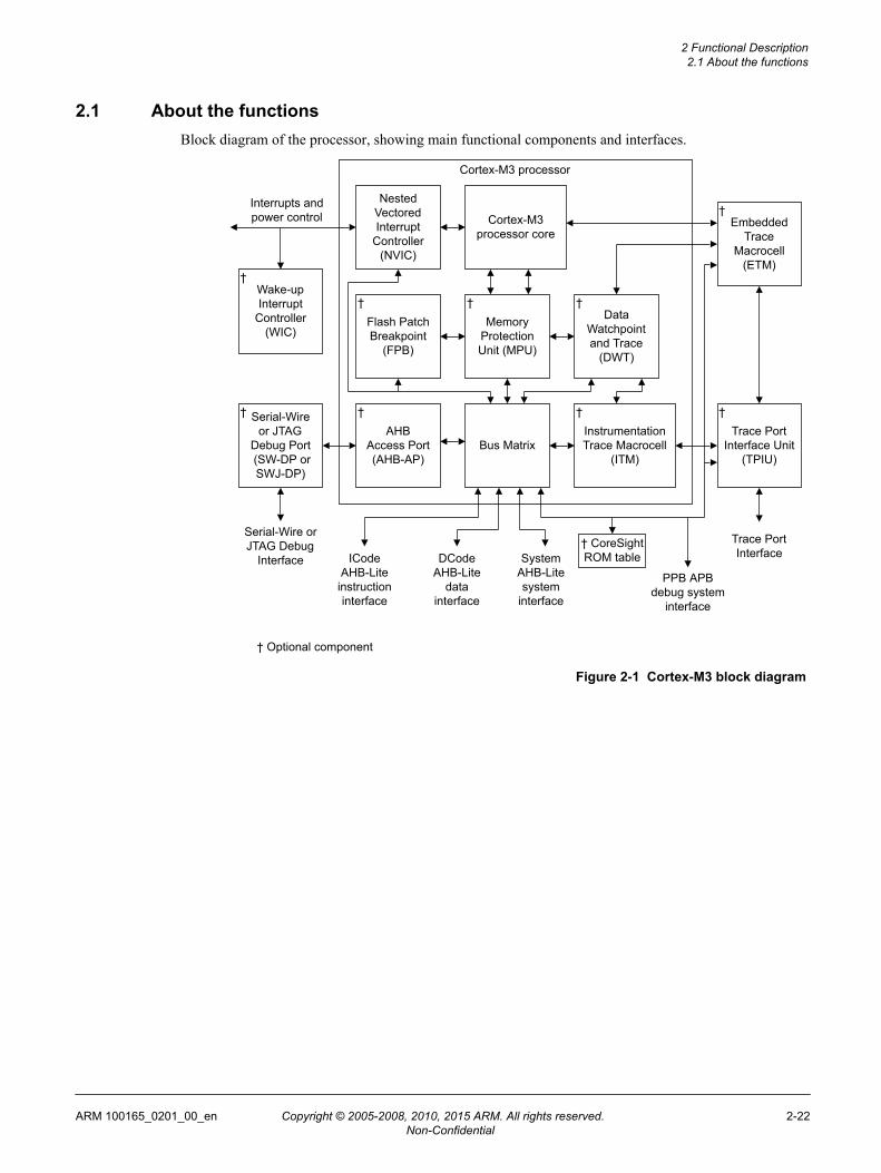
2.1 About the functionsBlock diagram of the processor, showing main functional components and interfaces.
†
†
Nested Vectored Interrupt
Controller (NVIC)
Bus Matrix
Cortex-M3 processor
Trace Port Interface
† CoreSight ROM table
Serial-Wire or JTAG Debug
Interface ICode AHB-Lite instruction interface
DCode AHB-Lite
data interface
System AHB-Lite system
interface
PPB APB debug system
interface
Interrupts and power control
Wake-up Interrupt
Controller (WIC)
Serial-Wireor JTAG
Debug Port (SW-DP or SWJ-DP)
† Embedded
Trace Macrocell
(ETM)
†
† Flash Patch Breakpoint
(FPB)
† Memory
ProtectionUnit (MPU)
† Data
Watchpoint and Trace
(DWT)
† AHB
Access Port (AHB-AP)
† Instrumentation Trace Macrocell
(ITM)
Trace Port Interface Unit
(TPIU)
Cortex-M3 processor core
† Optional component
Figure 2-1 Cortex-M3 block diagram
2 Functional Description2.1 About the functions
ARM 100165_0201_00_en Copyright © 2005-2008, 2010, 2015 ARM. All rights reserved. 2-22Non-Confidential
2.2 Processor features listThe processor features list includes a low gate count processor core, an optional memory protection unit,a low-cost debug solution, together with bus interfaces that includes three Advanced High-performanceBus-Lite (AHB-Lite) interfaces and a Private Peripheral Bus (PPB).
The processor features list comprises:• A low gate count processor core, with low latency interrupt processing that has:
— A subset of the Thumb instruction set, defined in the ARMv7-M Architecture Reference Manual.— Banked Stack Pointer (SP).— Hardware integer divide instructions, SDIV and UDIV.— Handler and Thread modes.— Thumb and Debug states.— Support for interruptible-continued instructions LDM, STM, PUSH, and POP for low interrupt latency.— Automatic processor state saving and restoration for low latency Interrupt Service Routine (ISR)
entry and exit.— Support for ARMv6 big-endian byte-invariant or little-endian accesses.— Support for ARMv6 unaligned accesses.
• Nested Vectored Interrupt Controller (NVIC) closely integrated with the processor core to achievelow latency interrupt processing. Features include:— External interrupts, configurable from 1 to 240.— Bits of priority, configurable from 3 to 8.— Dynamic reprioritization of interrupts.— Priority grouping. This enables selection of preempting interrupt levels and non preempting
interrupt levels.— Support for tail-chaining and late arrival of interrupts. This enables back-to-back interrupt
processing without the overhead of state saving and restoration between interrupts.— Processor state automatically saved on interrupt entry, and restored on interrupt exit, with no
instruction overhead.— Optional Wake-up Interrupt Controller (WIC), providing ultra-low power sleep mode support.
• Memory Protection Unit (MPU). An optional MPU for memory protection, including:— Eight memory regions.— Sub Region Disable (SRD), enabling efficient use of memory regions.— The ability to enable a background region that implements the default memory map attributes.
• Bus interfaces:— Three Advanced High-performance Bus-Lite (AHB-Lite) interfaces: ICode, DCode, and System
bus interfaces.— Private Peripheral Bus (PPB) based on Advanced Peripheral Bus (APB) interface.— Bit-band support that includes atomic bit-band write and read operations.— Memory access alignment.— Write buffer for buffering of write data.— Exclusive access transfers for multiprocessor systems.
• Low-cost debug solution that features:— Debug access to all memory and registers in the system, including access to memory mapped
devices, access to internal core registers when the core is halted, and access to debug controlregisters even while SYSRESETn is asserted.
— Serial Wire Debug Port (SW-DP) or Serial Wire JTAG Debug Port (SWJ-DP) debug access.— Optional Flash Patch and Breakpoint (FPB) unit for implementing breakpoints and code patches.— Optional Data Watchpoint and Trace (DWT) unit for implementing watchpoints, data tracing, and
system profiling.— Optional Instrumentation Trace Macrocell (ITM) for support of printf() style debugging.
2 Functional Description2.2 Processor features list
ARM 100165_0201_00_en Copyright © 2005-2008, 2010, 2015 ARM. All rights reserved. 2-23Non-Confidential
— Optional Trace Port Interface Unit (TPIU) for bridging to a Trace Port Analyzer (TPA),including Single Wire Output (SWO) mode.
— Optional Embedded Trace Macrocell (ETM) for instruction trace.
2 Functional Description2.2 Processor features list
ARM 100165_0201_00_en Copyright © 2005-2008, 2010, 2015 ARM. All rights reserved. 2-24Non-Confidential

2.3 InterfacesThe processor incorporates three external bus interfaces, an ETM interface that allows the connection ofan Embedded Trace Macrocell, an AHB Trace Macrocell interface that enables simple connection of anETM to the processor, and an Advanced High-performance Bus Access Port (AHB-AP) interface fordebug accesses.
This section contains the following subsections:• 2.3.1 Bus interfaces on page 2-25.• 2.3.2 ETM interface on page 2-26.• 2.3.3 AHB Trace Macrocell interface on page 2-27.• 2.3.4 Debug Port AHB-AP interface on page 2-27.
2.3.1 Bus interfaces
The Cortex-M3 processor contains three external Advanced High-performance Bus (AHB)-Lite businterfaces and one Advanced Peripheral Bus (APB) interface.
The processor matches the AMBA 3 specification except for maintaining control information duringwaited transfers. The AMBA 3 AHB-Lite Protocol states that when the slave is requesting wait states themaster must not change the transfer type, except for the following cases:• On an IDLE transfer, the master can change the transfer type from IDLE to NONSEQ.• On a BUSY transfer with a fixed length burst, the master can change the transfer type from BUSY to
SEQ.• On a BUSY transfer with an undefined length burst, the master can change the transfer type from
BUSY to any other transfer type.
The processor does not match this definition because it might change the access type from SEQ orNONSEQ to IDLE during a waited transfer. The processor might also change the address or othercontrol information and therefore request an access to a new location. The original address that wasretracted might not be requested again. This cancels the outstanding transfer that has not occurredbecause the previous access is wait-stated and awaiting completion. This is done so that the processorcan have a lower interrupt latency and higher performance in wait-stated systems by retracting accessesthat are no longer required.
To achieve complete compliance with the AMBA 3 specification you can implement the design with theAHB_CONST_CTRL parameter set to 1. This ensures that when transfers are issued during a wait-statedresponse they are never retracted or modified and the original transfer is honored. The consequence ofsetting this parameter is that the performance of the core might decrease for wait-stated systems as aresult of the interrupt and branch latency increasing.
ICode memory interface
Instruction fetches from Code memory space 0x00000000 to 0x1FFFFFFF are performed over the 32-bitAHB-Lite bus.
The Debugger cannot access this interface. All fetches are word-wide. The number of instructionsfetched per word depends on the code running and the alignment of the code in memory.
DCode memory interface
Data and debug accesses to Code memory space 0x00000000 to 0x1FFFFFFF are performed over the 32-bit AHB-Lite bus.
Core data accesses have a higher priority than debug accesses on this bus. This means that debugaccesses are waited until core accesses have completed when there are simultaneous core and debugaccess to this bus.
2 Functional Description2.3 Interfaces
ARM 100165_0201_00_en Copyright © 2005-2008, 2010, 2015 ARM. All rights reserved. 2-25Non-Confidential

Control logic in this interface converts unaligned data and debug accesses into two or three alignedaccesses, depending on the size and alignment of the unaligned access. This stalls any subsequent data ordebug access until the unaligned access has completed.
Note
ARM strongly recommends that any external arbitration between the ICode and DCode AHB businterfaces ensures that DCode has a higher priority than ICode.
System interface
Instruction fetches and data and debug accesses to address ranges 0x20000000 to 0xDFFFFFFF and0xE0100000 to 0xFFFFFFFF are performed over the 32-bit AHB-Lite bus.
For simultaneous accesses to the 32-bit AHB-Lite bus, the arbitration order in decreasing priority is:• Data accesses.• Instruction and vector fetches.• Debug.
The system bus interface contains control logic to handle unaligned accesses, FPB remapped accesses,bit-band accesses, and pipelined instruction fetches.
Private Peripheral Bus (PPB)
Data and debug accesses to external PPB space 0xE0040000 to 0xE00FFFFF are performed over the 32-bit Advanced Peripheral Bus (APB) bus.
The Trace Port Interface Unit (TPIU) and vendor specific peripherals are on the 32-bit AdvancedPeripheral Bus (APB) bus.
Core data accesses have higher priority than debug accesses, so debug accesses are waited until coreaccesses have completed when there are simultaneous core and debug accesses to this bus. Only theaddress bits necessary to decode the External PPB space are supported on this interface.
The External PPB (EPPB) space, 0xE0040000 up to 0xE0100000, is intended for CoreSight-compatibledebug and trace components, and has a number of irregular limitations which make it less useful forregular system peripherals. ARM recommends that system peripherals are placed in suitable Device typeareas of the System bus address space, with use of an AHB2APB protocol converter for APB-baseddevices.
Limitations of the EPPB space are:
• It is accessible in privileged mode only.• It is accessed in little-endian fashion irrespective of the data endianness setting of the processor.• Accesses behave as Strongly Ordered.• No bit-band function is available.• Unaligned accesses have Unpredictable results.• Only 32-bit data accesses are supported.• It is accessible from the Debug Port and the local processor, but not from any other processor in the
system.
2.3.2 ETM interface
The ETM interface enables simple connection of an ETM to the processor. It provides a channel forinstruction trace to the ETM.
See the ARM Embedded Trace Macrocell Architecture Specification.
2 Functional Description2.3 Interfaces
ARM 100165_0201_00_en Copyright © 2005-2008, 2010, 2015 ARM. All rights reserved. 2-26Non-Confidential
2.3.3 AHB Trace Macrocell interface
The AHB Trace Macrocell (HTM) interface enables a simple connection of the AHB trace macrocell tothe processor, and provides a channel for the data trace to the HTM.
Your implementation must include this interface to use the HTM interface. You must set TRCENA to 1in the Debug Exception and Monitor Control Register (DEMCR) before you enable the HTM port tosupply trace data. See the ARM®v7-M Architecture Reference Manual.
2.3.4 Debug Port AHB-AP interface
The processor contains an Advanced High-performance Bus Access Port (AHB-AP) interface for debugaccesses. An external Debug Port (DP) component accesses this interface.
The Cortex-M3 system supports three possible DP implementations:• The Serial Wire JTAG Debug Port (SWJ-DP). The SWJ-DP is a standard CoreSight debug port that
combines JTAG-DP and Serial Wire Debug Port (SW-DP).• The SW-DP. This provides a two-pin interface to the AHB-AP port.• No DP present. If no debug functionality is present within the processor, a DP is not required.
The two DP implementations provide different mechanisms for debug access to the processor. Yourimplementation must contain only one of these components.
Note
Your implementation might contain an alternative implementer-specific DP instead of SW-DP or SWJ-DP. See your implementer for details.
For more detailed information on the DP components, see the CoreSight™ Components TechnicalReference manual.
The DP and AP together are referred to as the Debug Access Port (DAP).
For more detailed information on the debug interface, see the ARM® Debug Interface v5 ArchitectureSpecification.
2 Functional Description2.3 Interfaces
ARM 100165_0201_00_en Copyright © 2005-2008, 2010, 2015 ARM. All rights reserved. 2-27Non-Confidential

Chapter 3Programmers Model
This chapter describes the processor programmers model.
It contains the following sections:• 3.1 About the programmers’ model on page 3-29.• 3.2 Modes of operation and execution on page 3-30.• 3.3 Instruction set summary on page 3-31.• 3.4 Processor memory model on page 3-37.• 3.5 Write buffer on page 3-40.• 3.6 Exclusive monitor on page 3-41.• 3.7 Bit-banding on page 3-42.• 3.8 Processor core register summary on page 3-44.• 3.9 Exceptions on page 3-46.
ARM 100165_0201_00_en Copyright © 2005-2008, 2010, 2015 ARM. All rights reserved. 3-28Non-Confidential
3.1 About the programmers’ modelThe Cortex-M3 programmers’ model describes the processor’s implementation-defined options.
For a complete description of the programmers’ model, refer to the ARM®v7-M Architecture ReferenceManual, which also contains the ARMv7-M Thumb instructions the model uses, and their cycle countsfor the processor. In addition, other options of the programmers’ model are described in the SystemControl, MPU, NVIC, FPU, Debug, DWT, ITM, and TPIU features topics.
3 Programmers Model3.1 About the programmers’ model
ARM 100165_0201_00_en Copyright © 2005-2008, 2010, 2015 ARM. All rights reserved. 3-29Non-Confidential

3.2 Modes of operation and executionThe Cortex-M3 processor supports Thread and Handler operating modes, and may be run in Thumb orDebug operating states. In addition, the processor can limit or exclude access to some resources byexecuting code in privileged or unprivileged mode.
See the ARM®v7-M Architecture Reference Manual for more information about these modes of operationand execution.
Operating modes
The conditions which cause the processor to enter Thread or Handler mode are as follows:• The processor enters Thread mode on Reset, or as a result of an exception return. Privileged and
Unprivileged code can run in Thread mode.• The processor enters Handler mode as a result of an exception. All code is privileged in Handler
mode.
Operating states
The processor can operate in thumb or debug state:• Thumb state. This is normal execution running 16-bit and 32-bit halfword aligned Thumb
instructions.• Debug State. This is the state when the processor is in halting debug.
Privileged access and user access
Handler mode is always privileged. Thread mode can be privileged or unprivileged.
3 Programmers Model3.2 Modes of operation and execution
ARM 100165_0201_00_en Copyright © 2005-2008, 2010, 2015 ARM. All rights reserved. 3-30Non-Confidential

3.3 Instruction set summaryThe processor implements the ARMv7-M Thumb instruction set, and is binary compatible with theinstruction sets and features implemented in other Cortex-M profile processors. Instructions can bepaired in a way that achieves optimum reductions in timing.
This section contains the following subsections:• 3.3.1 Processor instructions on page 3-31.• 3.3.2 Load/store timings on page 3-35.• 3.3.3 Binary compatibility with other Cortex processors on page 3-36.
3.3.1 Processor instructions
The table summarizes the Cortex-M3 processor instruction set. For brevity, not all load and storeaddressing modes are shown in the table. The cycle counts provided are based on a system with zero waitstates.
Within the assembler syntax, depending on the operation, the <op2> field can be replaced with one of thefollowing options:• A simple register specifier, for example Rm.• An immediate shifted register, for example Rm, LSL #4.• A register shifted register, for example Rm, LSL Rs.• An immediate value, for example #0xE000E000.
For brevity, not all load and store addressing modes are shown. See the ARMv7-M ArchitectureReference Manual for more information.
The following abbreviations are used in the Cycles column:
PThe number of cycles required for a pipeline refill. This ranges from 1 to 3 depending on thealignment and width of the target instruction, and whether the processor manages to speculatethe address early.
BThe number of cycles required to perform the barrier operation. For DSB and DMB, the minimumnumber of cycles is zero. For ISB, the minimum number of cycles is equivalent to the numberrequired for a pipeline refill.
NThe number of registers in the register list to be loaded or stored, including PC or LR.
WThe number of cycles spent waiting for an appropriate event.
Table 3-1 Cortex-M3 instruction set summary
Operation Description Assembler Cycles
Move Register MOV Rd, <op2> 1
16-bit immediate MOVW Rd, #<imm> 1
Immediate into top MOVT Rd, #<imm> 1
To PC MOV PC, Rm 1 + P
Add Add ADD Rd, Rn, <op2> 1
Add to PC ADD PC, PC, Rm 1 + P
Add with carry ADC Rd, Rn, <op2> 1
Form address ADR Rd, <label> 1
3 Programmers Model3.3 Instruction set summary
ARM 100165_0201_00_en Copyright © 2005-2008, 2010, 2015 ARM. All rights reserved. 3-31Non-Confidential
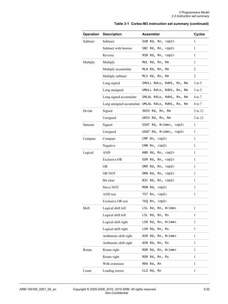
Table 3-1 Cortex-M3 instruction set summary (continued)
Operation Description Assembler Cycles
Subtract Subtract SUB Rd, Rn, <op2> 1
Subtract with borrow SBC Rd, Rn, <op2> 1
Reverse RSB Rd, Rn, <op2> 1
Multiply Multiply MUL Rd, Rn, Rm 1
Multiply accumulate MLA Rd, Rn, Rm 2
Multiply subtract MLS Rd, Rn, Rm 2
Long signed SMULL RdLo, RdHi, Rn, Rm 3 to 5
Long unsigned UMULL RdLo, RdHi, Rn, Rm 3 to 5
Long signed accumulate SMLAL RdLo, RdHi, Rn, Rm 4 to 7
Long unsigned accumulate UMLAL RdLo, RdHi, Rn, Rm 4 to 7
Divide Signed SDIV Rd, Rn, Rm 2 to 12
Unsigned UDIV Rd, Rn, Rm 2 to 12
Saturate Signed SSAT Rd, #<imm>, <op2> 1
Unsigned USAT Rd, #<imm>, <op2> 1
Compare Compare CMP Rn, <op2> 1
Negative CMN Rn, <op2> 1
Logical AND AND Rd, Rn, <op2> 1
Exclusive OR EOR Rd, Rn, <op2> 1
OR ORR Rd, Rn, <op2> 1
OR NOT ORN Rd, Rn, <op2> 1
Bit clear BIC Rd, Rn, <op2> 1
Move NOT MVN Rd, <op2> 1
AND test TST Rn, <op2> 1
Exclusive OR test TEQ Rn, <op1>
Shift Logical shift left LSL Rd, Rn, #<imm> 1
Logical shift left LSL Rd, Rn, Rs 1
Logical shift right LSR Rd, Rn, #<imm> 1
Logical shift right LSR Rd, Rn, Rs 1
Arithmetic shift right ASR Rd, Rn, #<imm> 1
Arithmetic shift right ASR Rd, Rn, Rs 1
Rotate Rotate right ROR Rd, Rn, #<imm> 1
Rotate right ROR Rd, Rn, Rs 1
With extension RRX Rd, Rn 1
Count Leading zeroes CLZ Rd, Rn 1
3 Programmers Model3.3 Instruction set summary
ARM 100165_0201_00_en Copyright © 2005-2008, 2010, 2015 ARM. All rights reserved. 3-32Non-Confidential
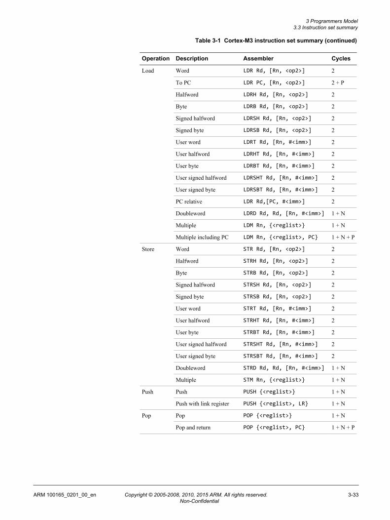
Table 3-1 Cortex-M3 instruction set summary (continued)
Operation Description Assembler Cycles
Load Word LDR Rd, [Rn, <op2>] 2
To PC LDR PC, [Rn, <op2>] 2 + P
Halfword LDRH Rd, [Rn, <op2>] 2
Byte LDRB Rd, [Rn, <op2>] 2
Signed halfword LDRSH Rd, [Rn, <op2>] 2
Signed byte LDRSB Rd, [Rn, <op2>] 2
User word LDRT Rd, [Rn, #<imm>] 2
User halfword LDRHT Rd, [Rn, #<imm>] 2
User byte LDRBT Rd, [Rn, #<imm>] 2
User signed halfword LDRSHT Rd, [Rn, #<imm>] 2
User signed byte LDRSBT Rd, [Rn, #<imm>] 2
PC relative LDR Rd,[PC, #<imm>] 2
Doubleword LDRD Rd, Rd, [Rn, #<imm>] 1 + N
Multiple LDM Rn, {<reglist>} 1 + N
Multiple including PC LDM Rn, {<reglist>, PC} 1 + N + P
Store Word STR Rd, [Rn, <op2>] 2
Halfword STRH Rd, [Rn, <op2>] 2
Byte STRB Rd, [Rn, <op2>] 2
Signed halfword STRSH Rd, [Rn, <op2>] 2
Signed byte STRSB Rd, [Rn, <op2>] 2
User word STRT Rd, [Rn, #<imm>] 2
User halfword STRHT Rd, [Rn, #<imm>] 2
User byte STRBT Rd, [Rn, #<imm>] 2
User signed halfword STRSHT Rd, [Rn, #<imm>] 2
User signed byte STRSBT Rd, [Rn, #<imm>] 2
Doubleword STRD Rd, Rd, [Rn, #<imm>] 1 + N
Multiple STM Rn, {<reglist>} 1 + N
Push Push PUSH {<reglist>} 1 + N
Push with link register PUSH {<reglist>, LR} 1 + N
Pop Pop POP {<reglist>} 1 + N
Pop and return POP {<reglist>, PC} 1 + N + P
3 Programmers Model3.3 Instruction set summary
ARM 100165_0201_00_en Copyright © 2005-2008, 2010, 2015 ARM. All rights reserved. 3-33Non-Confidential

Table 3-1 Cortex-M3 instruction set summary (continued)
Operation Description Assembler Cycles
Semaphore Load exclusive LDREX Rd, [Rn, #<imm>] 2
Load exclusive half LDREXH Rd, [Rn] 2
Load exclusive byte LDREXB Rd, [Rn] 2
Store exclusive STREX Rd, Rt, [Rn, #<imm>] 2
Store exclusive half STREXH Rd, Rt, [Rn] 2
Store exclusive byte STREXB Rd, Rt, [Rn] 2
Clear exclusive monitor CLREX 1
Branch Conditional B<cc> <label> 1 or 1 + P
Unconditional B <label> 1 + P
With link BL <label> 1 + P
With exchange BX Rm 1 + P
With link and exchange BLX Rm 1 + P
Branch if zero CBZ Rn, <label> 1 or 1 + P
Branch if non-zero CBNZ Rn, <label> 1 or 1 + P
Byte table branch TBB [Rn, Rm] 2 + P
Halfword table branch TBH [Rn, Rm, LSL#1] 2 + P
State change Supervisor call SVC #<imm> -
If-then-else IT... <cond> 1
Disable interrupts CPSID <flags> 1 or 2
Enable interrupts CPSIE <flags> 1 or 2
Read special register MRS Rd, <specreg> 1 or 2
Write special register MSR <specreg>, Rn 1 or 2
Breakpoint BKPT #<imm> -
Extend Signed halfword to word SXTH Rd, <op2> 1
Signed byte to word SXTB Rd, <op2> 1
Unsigned halfword UXTH Rd, <op2> 1
Unsigned byte UXTB Rd, <op2> 1
Bit field Extract unsigned UBFX Rd, Rn, #<imm>,#<imm>
1
Extract signed SBFX Rd, Rn, #<imm>,#<imm>
1
Clear BFC Rd, Rn, #<imm>, #<imm> 1
Insert BFI Rd, Rn, #<imm>, #<imm> 1
3 Programmers Model3.3 Instruction set summary
ARM 100165_0201_00_en Copyright © 2005-2008, 2010, 2015 ARM. All rights reserved. 3-34Non-Confidential

Table 3-1 Cortex-M3 instruction set summary (continued)
Operation Description Assembler Cycles
Reverse Bytes in word REV Rd, Rm 1
Bytes in both halfwords REV16 Rd, Rm 1
Signed bottom halfword REVSH Rd, Rm 1
Bits in word RBIT Rd, Rm 1
Hint Send event SEV 1
Wait for event WFE 1 + W
Wait for interrupt WFI 1 + W
No operation NOP 1
Barriers Instructionsynchronization
ISB 1 + B
Data memory DMB 1 + B
Data synchronization DSB <flags> 1 + B
The following notes apply to the information in the table:
• UMULL, SMULL, UMLAL, and SMLAL instructions use early termination depending on the size ofthe source values. These are interruptible, that is abandoned and restarted, with worst case latency ofone cycle.
• Neighboring load and store single instructions can pipeline their address and data phases. Thisenables these instructions to complete in a single execution cycle.
• For branch operations, conditional branch completes in a single cycle if the branch is not taken.• An IT instruction can be folded onto a preceding 16-bit Thumb instruction, enabling execution in
zero cycles.
3.3.2 Load/store timings
Instructions can be optimally paired to achieve more reductions in load and store timings.
The following information may help you to achieve further reductions in timing when pairinginstructions:• STR Rx,[Ry,#imm] is always one cycle. This is because the address generation is performed in the
initial cycle, and the data store is performed at the same time as the next instruction is executing. Ifthe store is to the write buffer, and the write buffer is full or not enabled, the next instruction isdelayed until the store can complete. If the store is not to the write buffer, for example to the Codesegment, and that transaction stalls, the impact on timing is only felt if another load or store operationis executed before completion.
• LDR PC,[any] is always a blocking operation. This means at least two cycles for the load, and threecycles for the pipeline reload. So this operation takes at least five cycles, or more if stalled on theload or the fetch.
• Any load or store that generates an address dependent on the result of a preceding data processingoperation stalls the pipeline for an additional cycle while the register bank is updated. There is noforwarding path for this scenario.
• LDR Rx,[PC,#imm] might add a cycle because of contention with the fetch unit.• TBB and TBH are also blocking operations. These are at least two cycles for the load, one cycle for the
add, and three cycles for the pipeline reload. This means at least six cycles, or more if stalled on theload or the fetch.
3 Programmers Model3.3 Instruction set summary
ARM 100165_0201_00_en Copyright © 2005-2008, 2010, 2015 ARM. All rights reserved. 3-35Non-Confidential

• LDR [any] are pipelined when possible. This means that if the next instruction is an LDR or STR, andthe destination of the first LDR is not used to compute the address for the next instruction, then onecycle is removed from the cost of the next instruction. So, an LDR might be followed by an STR, sothat the STR writes out what the LDR loaded. More multiple LDRs can be pipelined together. Someoptimized examples are:— LDR R0,[R1]; LDR R1,[R2] - normally three cycles total.— LDR R0,[R1,R2]; STR R0,[R3,#20] - normally three cycles total.— LDR R0,[R1,R2]; STR R1,[R3,R2] - normally three cycles total.— LDR R0,[R1,R5]; LDR R1,[R2]; LDR R2,[R3,#4] - normally four cycles total.
• Other instructions cannot be pipelined after STR with register offset. STR can only be pipelined whenit follows an LDR, but nothing can be pipelined after the store. Even a stalled STR normally only takestwo cycles, because of the write buffer.
• LDREX and STREX can be pipelined exactly as LDR. Because STREX is treated more like an LDR, it canbe pipelined as explained for LDR. Equally LDREX is treated exactly as an LDR and so can be pipelined.
• LDRD and STRD cannot be pipelined with preceding or following instructions. However, the two wordsare pipelined together. So, this operation requires three cycles when not stalled.
• LDM and STM cannot be pipelined with preceding or following instructions. However, all elementsafter the first are pipelined together. So, a three element LDM takes 2+1+1 or 5 cycles when notstalled. Similarly, an eight element store takes nine cycles when not stalled. When interrupted, LDMand STM instructions continue from where they left off when returned to. The continue operation addsone or two cycles to the first element when started.
• Unaligned word or halfword loads or stores add penalty cycles. A byte aligned halfword load or storeadds one extra cycle to perform the operation as two bytes. A halfword aligned word load or storeadds one extra cycle to perform the operation as two halfwords. A byte-aligned word load or storeadds two extra cycles to perform the operation as a byte, a halfword, and a byte. These numbersincrease if the memory stalls. A STR or STRH cannot delay the processor because of the write buffer.
Example graphic
ReservedReserved
31 3 2 1 0
DISFOLDDISDEFWBUFDISMCYCINT
10 9 8 7
DISFPCADISOOFP
3.3.3 Binary compatibility with other Cortex processors
The processor implements a subset of the instruction set and features provided by the ARMv7-Marchitecture profile, and is binary compatible with the instruction sets and features implemented in otherCortex-M profile processors. You can move software, including system level software, from theCortex-M3 processor to other Cortex-M profile processors.
To ensure a smooth transition, ARM recommends that code designed to operate on other Cortex-Mprofile processor architectures obey the following rules and configure the Configuration and ControlRegister (CCR) appropriately:• Use word transfers only to access registers in the NVIC and System Control Space (SCS).• Treat all unused SCS registers and register fields on the processor as Do-Not-Modify.• Configure the following fields in the CCR:
— STKALIGN bit to 1.— UNALIGN_TRP bit to 1.— Leave all other bits in the CCR register as their original value.
3 Programmers Model3.3 Instruction set summary
ARM 100165_0201_00_en Copyright © 2005-2008, 2010, 2015 ARM. All rights reserved. 3-36Non-Confidential
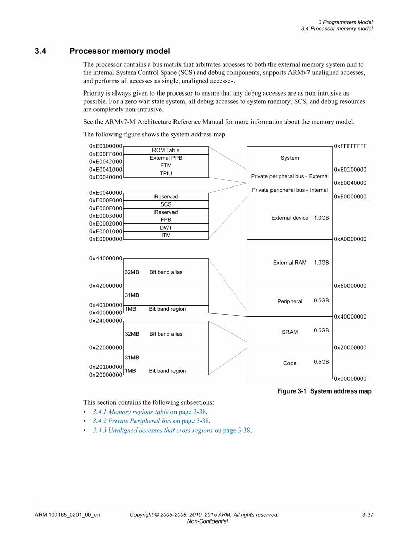
3.4 Processor memory modelThe processor contains a bus matrix that arbitrates accesses to both the external memory system and tothe internal System Control Space (SCS) and debug components, supports ARMv7 unaligned accesses,and performs all accesses as single, unaligned accesses.
Priority is always given to the processor to ensure that any debug accesses are as non-intrusive aspossible. For a zero wait state system, all debug accesses to system memory, SCS, and debug resourcesare completely non-intrusive.
See the ARMv7-M Architecture Reference Manual for more information about the memory model.
The following figure shows the system address map.
System
External device
External RAM
Peripheral
SRAM
Code
0xFFFFFFFF
Private peripheral bus - External0xE0100000
0xE0040000
0xA0000000
0x60000000
0x40000000
0x20000000
0x00000000
ROM Table
ETMTPIU
ReservedSCS
ReservedFPBDWTITM
External PPB0xE00420000xE00410000xE0040000
0xE000F0000xE000E0000xE00030000xE0002000
0xE00FF000
0x40000000 Bit band region
Bit band alias32MB
1MB
31MB
0x40100000
0x42000000
0x44000000
0xE00010000xE0000000
Private peripheral bus - Internal
Bit band region
Bit band alias32MB
1MB
31MB
0x200000000x20100000
0x22000000
1.0GB
1.0GB
0.5GB
0.5GB
0.5GB
0xE0000000
0xE0100000
0xE0040000
0x24000000
Figure 3-1 System address map
This section contains the following subsections:• 3.4.1 Memory regions table on page 3-38.• 3.4.2 Private Peripheral Bus on page 3-38.• 3.4.3 Unaligned accesses that cross regions on page 3-38.
3 Programmers Model3.4 Processor memory model
ARM 100165_0201_00_en Copyright © 2005-2008, 2010, 2015 ARM. All rights reserved. 3-37Non-Confidential

3.4.1 Memory regions table
The table shows the processor interfaces that are addressed by the different memory map regions.
Table 3-2 Memory regions
Memory Map Region
Code Instruction fetches are performed over the ICode bus. Data accesses are performed over the DCode bus.
SRAM Instruction fetches and data accesses are performed over the system bus.
SRAM bit-band Alias region. Data accesses are aliases. Instruction accesses are not aliases.
Peripheral Instruction fetches and data accesses are performed over the system bus.
Peripheral bit-band Alias region. Data accesses are aliases. Instruction accesses are not aliases.
External RAM Instruction fetches and data accesses are performed over the system bus.
External Device Instruction fetches and data accesses are performed over the system bus.
Private Peripheral Bus External and internal Private Peripheral Bus (PPB) interfaces.
This memory region is Execute Never (XN), and so instruction fetches are prohibited. An MPU, if present,cannot change this.
System System segment for vendor system peripherals. This memory region is XN, and so instruction fetches areprohibited. An MPU, if present, cannot change this.
3.4.2 Private Peripheral Bus
The Private Peripheral Bus (PPB) interface provides access to internal and external processor resources.
The internal Private Peripheral Bus (PPB) interface provides access to:• The Instrumentation Trace Macrocell (ITM).• The Data Watchpoint and Trace (DWT).• The Flashpatch and Breakpoint (FPB).• The System Control Space (SCS), including the Memory Protection Unit (MPU) and the Nested
Vectored Interrupt Controller (NVIC).
The external PPB interface provides access to:
• The Trace Point Interface Unit (TPIU).• The Embedded Trace Macrocell (ETM).• The ROM table.• Implementation-specific areas of the PPB memory map.
3.4.3 Unaligned accesses that cross regions
The Cortex-M3 processor supports ARMv7 unaligned accesses, and performs all accesses as single,unaligned accesses. They are converted into two or more aligned accesses by the DCode and System businterfaces.
Note
All Cortex-M3 external accesses are aligned.
Unaligned support is only available for load/store singles (LDR, LDRH, STR, STRH). Load/store doublealready supports word aligned accesses, but does not permit other unaligned accesses, and generates afault if this is attempted.
3 Programmers Model3.4 Processor memory model
ARM 100165_0201_00_en Copyright © 2005-2008, 2010, 2015 ARM. All rights reserved. 3-38Non-Confidential

Unaligned accesses that cross memory map boundaries are architecturally UNPREDICTABLE. The processorbehavior is boundary dependent, as follows:
• DCode accesses wrap within the region. For example, an unaligned halfword access to the last byteof Code space (0x1FFFFFFF) is converted by the DCode interface into a byte access to 0x1FFFFFFFfollowed by a byte access to 0x00000000.
• System accesses that cross into PPB space do not wrap within System space. For example, anunaligned halfword access to the last byte of System space (0xDFFFFFFF) is converted by the Systeminterface into a byte access to 0xDFFFFFFF followed by a byte access to 0xE0000000. 0xE0000000 isnot a valid address on the System bus.
• System accesses that cross into Code space do not wrap within System space. For example, anunaligned halfword access to the last byte of System space (0xFFFFFFFF) is converted by the Systeminterface into a byte access to 0xFFFFFFFF followed by a byte access to 0x00000000. 0x00000000 isnot a valid address on the System bus.
• Unaligned accesses are not supported to PPB space, and so there are no boundary crossing cases forPPB accesses.
Unaligned accesses that cross into the bit-band alias regions are also architecturally UNPREDICTABLE. Theprocessor performs the access to the bit-band alias address, but this does not result in a bit-bandoperation. For example, an unaligned halfword access to 0x21FFFFFF is performed as a byte access to0x21FFFFFF followed by a byte access to 0x22000000 (the first byte of the bit-band alias).
Unaligned loads that match against a literal comparator in the FPB are not remapped. FPB only remapsaligned addresses.
3 Programmers Model3.4 Processor memory model
ARM 100165_0201_00_en Copyright © 2005-2008, 2010, 2015 ARM. All rights reserved. 3-39Non-Confidential

3.5 Write bufferTo prevent bus wait cycles from stalling the processor during data stores, buffered stores to the DCodeand System buses go through a one-entry write buffer. If the write buffer is full, subsequent accesses tothe bus stall until the write buffer has drained.
The write buffer is only used if the bus waits the data phase of the buffered store, otherwise thetransaction completes on the bus.
DMB and DSB instructions wait for the write buffer to drain before completing. If an interrupt comes inwhile DMB or DSB is waiting for the write buffer to drain, the processor returns to the instruction followingthe DMB or DSB after the interrupt completes. This is because interrupt processing acts as a memory barrieroperation.
3 Programmers Model3.5 Write buffer
ARM 100165_0201_00_en Copyright © 2005-2008, 2010, 2015 ARM. All rights reserved. 3-40Non-Confidential

3.6 Exclusive monitorThe Cortex-M3 processor implements a local exclusive monitor. The local monitor within the processorhas been constructed so that it does not hold any physical address, but instead treats any access asmatching the address of the previous LDREX. This means that the implemented exclusives reservationgranule is the entire memory address range.
The Cortex-M3 processor does not support exclusive accesses to bit-band regions.
For more information about semaphores and the local exclusive monitor, see the ARM®v7-M ArchitectureReference Manual.
3 Programmers Model3.6 Exclusive monitor
ARM 100165_0201_00_en Copyright © 2005-2008, 2010, 2015 ARM. All rights reserved. 3-41Non-Confidential

3.7 Bit-bandingBit-banding is an optional feature of the Cortex-M3 processor. Bit-banding maps a complete word ofmemory onto a single bit in the bit-band region. For example, writing to one of the alias words sets orclears the corresponding bit in the bit-band region.
This section contains the following subsections:• 3.7.1 About bit-banding on page 3-42.• 3.7.2 Directly accessing an alias region on page 3-43.• 3.7.3 Directly accessing a bit-band region on page 3-43.
3.7.1 About bit-banding
Bit-banding enables every individual bit in the bit-banding region to be directly accessible from a word-aligned address using a single LDR instruction. It also enables individual bits to be toggled withoutperforming a read-modify-write sequence of instructions.
The processor memory map includes two bit-band regions. These occupy the lowest 1MB of the SRAMand Peripheral memory regions respectively. These bit-band regions map each word in an alias region ofmemory to a bit in a bit-band region of memory.
The System bus interface contains logic that controls bit-band accesses as follows:
• It remaps bit-band alias addresses to the bit-band region.• For reads, it extracts the requested bit from the read byte, and returns this in the Least Significant Bit
(LSB) of the read data returned to the core.• For writes, it converts the write to an atomic read-modify-write operation.• The processor does not stall during bit-band operations unless it attempts to access the System bus
while the bit-band operation is being carried out.
The memory map has two 32MB alias regions that map to two 1MB bit-band regions:
• Accesses to the 32MB SRAM alias region map to the 1MB SRAM bit-band region.• Accesses to the 32MB peripheral alias region map to the 1MB peripheral bit-band region.
A mapping formula shows how to reference each word in the alias region to a corresponding bit, ortarget bit, in the bit-band region. The mapping formula is:
bit_word_offset = (byte_offset × 32) + (bit_number × 4)
bit_word_addr = bit_band_base + bit_word_offset
where:
• bit_word_offset is the position of the target bit in the bit-band memory region.• bit_word_addr is the address of the word in the alias memory region that maps to the targeted bit.• bit_band_base is the starting address of the alias region.• byte_offset is the number of the byte in the bit-band region that contains the targeted bit.• bit_number is the bit position, 0 to 7, of the targeted bit.
The following figure shows examples of bit-band mapping between the SRAM bit-band alias region andthe SRAM bit-band region:
• The alias word at 0x23FFFFE0 maps to bit [0] of the bit-band byte at 0x200FFFFF: 0x23FFFFE0 =0x22000000 + (0xFFFFF*32) + 0*4.
• The alias word at 0x23FFFFFC maps to bit [7] of the bit-band byte at 0x200FFFFF: 0x23FFFFFC =0x22000000 + (0xFFFFF*32) + 7*4.
• The alias word at 0x22000000 maps to bit [0] of the bit-band byte at 0x20000000: 0x22000000 =0x22000000 + (0*32) + 0*4.
3 Programmers Model3.7 Bit-banding
ARM 100165_0201_00_en Copyright © 2005-2008, 2010, 2015 ARM. All rights reserved. 3-42Non-Confidential

• The alias word at 0x2200001C maps to bit [7] of the bit-band byte at 0x20000000: 0x2200001C =0x22000000 + (0*32) + 7*4.
0x23FFFFE4
0x22000004
0x23FFFFE00x23FFFFE80x23FFFFEC0x23FFFFF00x23FFFFF40x23FFFFF80x23FFFFFC
0x220000000x220000140x220000180x2200001C 0x220000080x22000010 0x2200000C
32MB alias region
0
7 0
07
0x200000000x200000010x200000020x20000003
6 5 4 3 2 1 07 6 5 4 3 2 1 7 6 5 4 3 2 1 07 6 5 4 3 2 1
07 6 5 4 3 2 1 6 5 4 3 2 107 6 5 4 3 2 1 07 6 5 4 3 2 1
0x200FFFFC0x200FFFFD0x200FFFFE0x200FFFFF
1MB SRAM bit-band region
Figure 3-2 Bit-band mapping
3.7.2 Directly accessing an alias region
Writing to a word in the alias region has the same effect as a read-modify-write operation on the targetedbit in the bit-band region.
Bit [0] of the value written to a word in the alias region determines the value written to the targeted bit inthe bit-band region. Writing a value with bit [0] set writes a 1 to the bit-band bit, and writing a value withbit [0] cleared writes a 0 to the bit-band bit.
Bits [31:1] of the alias word have no effect on the bit-band bit. Writing 0x01 has the same effect aswriting 0xFF. Writing 0x00 has the same effect as writing 0x0E.
Reading a word in the alias region returns either 0x01 or 0x00. A value of 0x01 indicates that thetargeted bit in the bit-band region is set. A value of 0x00 indicates that the targeted bit is clear. Bits[31:1] are zero.
3.7.3 Directly accessing a bit-band region
You can directly access the bit-band region with normal reads and writes to that region.
3 Programmers Model3.7 Bit-banding
ARM 100165_0201_00_en Copyright © 2005-2008, 2010, 2015 ARM. All rights reserved. 3-43Non-Confidential

3.8 Processor core register summaryThe processor has 32-registers that includes 13 general-purpose registers and several special-purposeregisters.
The processor has the following 32-bit registers:• 13 general-purpose registers, R0-R12.• Stack Pointer (SP), R13 alias of banked registers, SP_process and SP_main.• Link Register (LR), R14.• Program Counter (PC), R15.• Special-purpose Program Status Registers, (xPSR).
The following figure shows the processor register set.
Program Status Register
R13 (SP)R14 (LR)R15 (PC)
R5R6R7
R0R1
R3R4
R2
R10R11R12
R8R9
low registers
high registers
SP_mainSP_process
xPSR
Figure 3-3 Processor register set
The general-purpose registers R0-R12 have no special architecturally-defined uses. Most instructionsthat can specify a general-purpose register can specify R0-R12.
Low registersRegisters R0-R7 are accessible by all instructions that specify a general-purpose register.
High registersRegisters R8-R12 are accessible by all 32-bit instructions that specify a general-purposeregister.
Registers R8-R12 are not accessible by any 16-bit instructions.
Registers R13, R14, and R15 have the following special functions:
Stack pointerRegister R13 is used as the Stack Pointer (SP). Because the SP ignores writes to bits [1:0], it isautoaligned to a word, four-byte boundary.
Handler mode always uses SP_main, but you can configure Thread mode to use either SP_mainor SP_process.
3 Programmers Model3.8 Processor core register summary
ARM 100165_0201_00_en Copyright © 2005-2008, 2010, 2015 ARM. All rights reserved. 3-44Non-Confidential

Link registerRegister R14 is the subroutine Link Register (LR).
The LR receives the return address from PC when a Branch and Link (BL) or Branch and Linkwith Exchange (BLX) instruction is executed.
The LR is also used for exception return.
At all other times, you can treat R14 as a general-purpose register.
Program counterRegister R15 is the Program Counter (PC).
Bit [0] is always 0, so instructions are always aligned to word or halfword boundaries.
See the ARMv7-M Architecture Reference Manual for more information.
3 Programmers Model3.8 Processor core register summary
ARM 100165_0201_00_en Copyright © 2005-2008, 2010, 2015 ARM. All rights reserved. 3-45Non-Confidential

3.9 ExceptionsExceptions are handled and prioritized by the processor and the NVIC. In addition to architecturallydefined behavior, the processor implements advanced exception and interrupt handling that reducesinterrupt latency and includes implementation defined behavior.
This section contains the following subsections:• 3.9.1 Exception handling and prioritization on page 3-46.• 3.9.2 Interrupt latency on page 3-46.• 3.9.3 Base register update in LDM and STM operations on page 3-47.
3.9.1 Exception handling and prioritization
The processor and the Nested Vectored Interrupt Controller (NVIC) prioritize and handle all exceptions.
When handling exceptions:• All exceptions are handled in Handler mode.• Processor state is automatically stored to the stack on an exception, and automatically restored from
the stack at the end of the Interrupt Service Routine (ISR).• The vector is fetched in parallel to the state saving, enabling efficient interrupt entry.
The processor supports tail-chaining that enables back-to-back interrupts without the overhead of statesaving and restoration.
You configure the number of interrupts, and bits of interrupt priority, during implementation. Softwarecan choose only to enable a subset of the configured number of interrupts, and can choose how many bitsof the configured priorities to use.
Note
Vector table entries are compatible with interworking between ARM and Thumb instructions. Thiscauses bit [0] of the vector value to load into the Execution Program Status Register (EPSR) T-bit onexception entry. All populated vectors in the vector table entries must have bit [0] set. Creating a tableentry with bit [0] clear generates an INVSTATE fault on the first instruction of the handlercorresponding to this vector.
3.9.2 Interrupt latency
The processor implements advanced exception and interrupt handling that reduces interrupt latency, andincludes implementation defined behavior in addition to the architecturally defined behavior.
To reduce interrupt latency, the processor implements both interrupt late-arrival and interrupt tail-chaining mechanisms, as defined by the ARMv7-M architecture:• There is a maximum of a twelve cycle latency from asserting the interrupt to execution of the first
instruction of the ISR when the memory being accessed has no wait states being applied. The firstinstruction to be executed is fetched in parallel to the stack push.
• Returns from interrupts similarly take twelve cycles where the instruction being returned to is fetchedin parallel to the stack pop.
• Tail chaining requires six cycles when using zero wait state memory. No stack pushes or pops areperformed and only the instruction for the next ISR is fetched.
The processor exception model has the following implementation-defined behavior in addition to thearchitecturally defined behavior:
• Exceptions on stacking from HardFault to NMI lockup at NMI priority.• Exceptions on unstacking from NMI to HardFault lockup at HardFault priority.
To minimize interrupt latency, the processor abandons any divide instruction to take any pendinginterrupt. On return from the interrupt handler, the processor restarts the divide instruction from the
3 Programmers Model3.9 Exceptions
ARM 100165_0201_00_en Copyright © 2005-2008, 2010, 2015 ARM. All rights reserved. 3-46Non-Confidential

beginning. The processor implements the Interruptible-continuable Instruction field. Load multiple (LDM)operations and store multiple (STM) operations are interruptible. The EPSR holds the informationrequired to continue the load or store multiple from the point where the interrupt occurred.
This means that software must not use load-multiple or store-multiple instructions to access a device oraccess a memory region that is read-sensitive or sensitive to repeated writes. The software must not usethese instructions in any case where repeated reads or writes might cause inconsistent results orunwanted side-effects.
For more information, see the ARMv7-M Architecture Reference Manual.
3.9.3 Base register update in LDM and STM operations
When the instruction specifies base register write-back, the base register changes to the updated address(an abort restores the original base value). When the base register is in the register list of an LDM, and isnot the last register in the list, the base register changes to the loaded value.
An LDM or STM is restarted rather than continued if:• The instruction faults.• The instruction is inside an IT.
If an LDM has completed a base load, it is continued from before the base load.
3 Programmers Model3.9 Exceptions
ARM 100165_0201_00_en Copyright © 2005-2008, 2010, 2015 ARM. All rights reserved. 3-47Non-Confidential

Chapter 4System Control
This chapter provides a summary of the system control registers whose implementation is specific to theCortex-M3 processor.
Registers not described here are described in the ARM®v7-M Architecture Reference Manual.
It contains the following sections:• 4.1 System control registers on page 4-49.• 4.2 Auxiliary Control Register, ACTLR on page 4-51.• 4.3 CPUID Base Register, CPUID on page 4-52.• 4.4 Auxiliary Fault Status Register, AFSR on page 4-53.
ARM 100165_0201_00_en Copyright © 2005-2008, 2010, 2015 ARM. All rights reserved. 4-48Non-Confidential

4.1 System control registersList of system control registers whose implementation is specific to the Cortex-M3 processor.
Registers not described in the table are described in the ARMv7-M Architecture Reference Manual.
Table 4-1 System control registers
Address Name Type Reset Description
0xE000E008 ACTLR RW 0x00000000 Refer to the Auxiliary Control Register, ACTLR
0xE000E010 STCSR RW 0x00000000 SysTick Control and Status Register
0xE000E014 STRVR RW Unknown SysTick Reload Value Register
0xE000E018 STCVR RW clear Unknown SysTick Current Value Register
0xE000E01C STCR RO Implementation specific SysTick Calibration Value Register
0xE000ED00 CPUID RO 0x412FC231 Refer to the CPUID Base Register, CPUID
0xE000ED04 ICSR RW or RO 0x00000000 Interrupt Control and State Register
0xE000ED08 VTOR RW 0x00000000 Vector Table Offset Register
0xE000ED0C AIRCR RW 0x00000000 Application Interrupt and Reset Control Register. Bits [10:8] arereset to zero. The ENDIANNESS bit, bit [15], can reset to eitherstate, depending on the implementation.
0xE000ED10 SCR RW 0x00000000 System Control Register
0xE000ED14 CCR RW 0x00000200 Configuration and Control Register.
0xE000ED18 SHPR1 RW 0x00000000 System Handler Priority Register 1
0xE000ED1C SHPR2 RW 0x00000000 System Handler Priority Register 2
0xE000ED20 SHPR3 RW 0x00000000 System Handler Priority Register 3
0xE000ED24 SHCSR RW 0x00000000 System Handler Control and State Register
0xE000ED28 CFSR RW 0x00000000 Configurable Fault Status Registers
0xE000ED2C HFSR RW 0x00000000 HardFault Status Register
0xE000ED30 DFSR RW 0x00000000 Debug Fault Status Register
0xE000ED34 MMFAR RW Unknown MemManage Fault Address Register. BFAR and MMFAR are thesame physical register. Because of this, the BFARVALID andMMFARVALID bits are mutually exclusive.
0xE000ED38 BFAR RW Unknown BusFault Address Register. BFAR and MMFAR are the samephysical register. Because of this, the BFARVALID andMMFARVALID bits are mutually exclusive.
0xE000ED3C AFSR RW 0x00000000 Refer to the Auxiliary Fault Status Register
0xE000ED40 ID_PFR0 RO 0x00000030 Processor Feature Register 0
0xE000ED44 ID_PFR1 RO 0x00000200 Processor Feature Register 1
0xE000ED48 ID_DFR0 RO 0x00100000 Debug Features Register 0. BFAR and MMFAR are the samephysical register. Because of this, the BFARVALID andMMFARVALID bits are mutually exclusive.
0xE000ED4C ID_AFR0 RO 0x00000000 Auxiliary Features Register 0
4 System Control4.1 System control registers
ARM 100165_0201_00_en Copyright © 2005-2008, 2010, 2015 ARM. All rights reserved. 4-49Non-Confidential

Table 4-1 System control registers (continued)
Address Name Type Reset Description
0xE000ED50 ID_MMFR0 RO 0x00100030 Memory Model Feature Register 0
0xE000ED54 ID_ MMFR1 RO 0x00000000 Memory Model Feature Register 1
0xE000ED58 ID_MMFR2 RO 0x01000000 Memory Model Feature Register 2
0xE000ED5C ID_MMFR3 RO 0x00000000 Memory Model Feature Register 3
0xE000ED60 ID_ISAR0 RO 0x01100110 Instruction Set Attributes Register 0
0xE000ED64 ID_ISAR1 RO 0x02111000 Instruction Set Attributes Register 1
0xE000ED68 ID_ISAR2 RO 0x21112231 Instruction Set Attributes Register 2
0xE000ED6C ID_ISAR3 RO 0x01111110 Instruction Set Attributes Register 3
0xE000ED70 ID_ISAR4 RO 0x01310132 Instruction Set Attributes Register 4
0xE000ED88 CPACR RW 0x00000000 Coprocessor Access Control Register
0xE000EF00 STIR WO 0x00000000 Software Triggered Interrupt Register
4 System Control4.1 System control registers
ARM 100165_0201_00_en Copyright © 2005-2008, 2010, 2015 ARM. All rights reserved. 4-50Non-Confidential

4.2 Auxiliary Control Register, ACTLRCharacteristics and bit assignments of the ACTLR register.
PurposeDisables certain aspects of functionality within the processor.
Usage ConstraintsThere are no usage constraints.
ConfigurationsThis register is available in all processor configurations.
AttributesSee the System control registers table.
The following figure shows the ACTLR bit assignments.
ReservedReserved
31 3 2 1 0
DISFOLDDISDEFWBUFDISMCYCINT
10 9 8 7
DISFPCADISOOFP
Figure 4-1 ACTLR bit assignments
The following table shows the ACTLR bit assignments.
Table 4-2 ACTLR bit assignments
Bits Name Function
[31:10] - Reserved.
[9] DISOOFP Disables floating point instructions completing out of order with respect to integer instructions.
[8] DISFPCA SBZP.
[7:3] - Reserved
[2] DISFOLD Disables folding of IT instructions.
[1] DISDEFWBUF Disables write buffer use during default memory map accesses. This causes all bus faults to be precise, butdecreases the performance of the processor because stores to memory must complete before the nextinstruction can be executed.
[0] DISMCYCINT Disables interruption of multi-cycle instructions. This increases the interrupt latency of the processorbecause load/store and multiply/divide operations complete before interrupt stacking occurs.
4 System Control4.2 Auxiliary Control Register, ACTLR
ARM 100165_0201_00_en Copyright © 2005-2008, 2010, 2015 ARM. All rights reserved. 4-51Non-Confidential

4.3 CPUID Base Register, CPUIDCharacteristics and bit assignments of the CPUID register.
PurposeSpecifies:• The ID number of the processor core.• The version number of the processor core.• The implementation details of the processor core.
Usage ConstraintsThere are no usage constraints.
ConfigurationsThis register is available in all processor configurations.
AttributesDescribed in the System control registers table.
The following figure shows the CPUID bit assignments.
31 16 15 4 3 0
IMPLEMENTER REVISIONPARTNO
24 23 20 19
VARIANT (Constant)
Figure 4-2 CPUID bit assignments
The following table shows the CPUID bit assignments.
Table 4-3 CPUID bit assignments
Bits NAME Function
[31:24] IMPLEMENTER Indicates implementer: 0x41 = ARM
[23:20] VARIANT Indicates processor revision: 0x0 = Revision 0
[19:16] (Constant) Reads as 0xF
[15:4] PARTNO Indicates part number: 0xC24 = Cortex-M3
[3:0] REVISION Indicates patch release: 0x1= Patch 1.
4 System Control4.3 CPUID Base Register, CPUID
ARM 100165_0201_00_en Copyright © 2005-2008, 2010, 2015 ARM. All rights reserved. 4-52Non-Confidential

4.4 Auxiliary Fault Status Register, AFSRCharacteristics and bit assignments of the AFSR register.
PurposeSpecifies additional system fault information to software.
Usage ConstraintsThe AFSR flags map directly onto the AUXFAULT inputs of the processor, and a single-cyclehigh level on an external pin causes the corresponding AFSR bit to become latched as one. Thebit can only be cleared by writing a one to the corresponding AFSR bit.
When an AFSR bit is written or latched as one, an exception does not occur. To make use ofAUXFAULT input signals, software must poll the AFSR.
ConfigurationsThis register is available in all processor configurations.
AttributesSee the System control registers table.
The following figure shows the AFSR bit assignments.
AUXFAULT
31 0
Figure 4-3 AFSR bit assignments
The following table shows the AFSR bit assignments.
Table 4-4 AFSR bit assignments
Bits Name Function
[31:0] AUXFAULT Latched version of the AUXFAULT inputs.
4 System Control4.4 Auxiliary Fault Status Register, AFSR
ARM 100165_0201_00_en Copyright © 2005-2008, 2010, 2015 ARM. All rights reserved. 4-53Non-Confidential

Chapter 5Memory Protection Unit
This chapter describes the processor Memory Protection Unit (MPU).
It contains the following sections:• 5.1 About the MPU on page 5-55.• 5.2 MPU functional description on page 5-56.• 5.3 MPU programmers model table on page 5-57.
ARM 100165_0201_00_en Copyright © 2005-2008, 2010, 2015 ARM. All rights reserved. 5-54Non-Confidential

5.1 About the MPUThe MPU enforces privilege rules, separates processes, and enforces access rules to memory. The MPUis an optional component and supports the standard ARMv7 Protected Memory System Architecturemodel.
The MPU provides full support for:• Protection regions.• Overlapping protection regions, with ascending region priority:
— 7 = highest priority.— 0 = lowest priority.
• Access permissions.• Exporting memory attributes to the system.
MPU mismatches and permission violations invoke the programmable-priority MemManage faulthandler. See the ARM®v7-M Architecture Reference Manual for more information.
You can use the MPU to:
• Enforce privilege rules.• Separate processes.• Enforce access rules.
5 Memory Protection Unit5.1 About the MPU
ARM 100165_0201_00_en Copyright © 2005-2008, 2010, 2015 ARM. All rights reserved. 5-55Non-Confidential

5.2 MPU functional descriptionThe access permission bits, TEX, C, B, AP, and XN, of the Region Access Control Register controlaccess to the corresponding memory region. If an access is made to an area of memory without therequired permissions, a permission fault is raised.
For more information, see the ARM®v7-M Architecture Reference Manual.
5 Memory Protection Unit5.2 MPU functional description
ARM 100165_0201_00_en Copyright © 2005-2008, 2010, 2015 ARM. All rights reserved. 5-56Non-Confidential

5.3 MPU programmers model tableTable of MPU registers, with address, name, type, reset, and description information.
These registers are described in the ARMv7-M Architecture Reference Manual.
Table 5-1 MPU registers
Address Name Type Reset Description
0xE000ED90 MPU_TYPE RO 0x00000800 MPU Type Register
If the MPU is not present in the implementation this register reads as zero.
0xE000ED94 MPU_CTRL RW 0x00000000 MPU Control Register
0xE000ED98 MPU_RNR RW 0x00000000 MPU Region Number Register
0xE000ED9C MPU_RBAR RW 0x00000000 MPU Region Base Address Register
0xE000EDA0 MPU_RASR RW 0x00000000 MPU Region Attribute and Size Register
0xE000EDA4 MPU_RBAR_A1 0x00000000 MPU alias registers
0xE000EDA8 MPU_RASR_A1 0x00000000
0xE000EDAC MPU_RBAR_A2 0x00000000
0xE000EDB0 MPU_RASR_A2 0x00000000
0xE000EDB4 MPU_RBAR_A3 0x00000000
0xE000EDB8 MPU_RASR_A3 0x00000000
5 Memory Protection Unit5.3 MPU programmers model table
ARM 100165_0201_00_en Copyright © 2005-2008, 2010, 2015 ARM. All rights reserved. 5-57Non-Confidential
Chapter 6Nested Vectored Interrupt Controller
This chapter describes the Nested Vectored Interrupt Controller (NVIC). The NVIC providesconfigurable interrupt handling abilities to the processor, facilitates low- latency exception and interrupthandling, and controls power management.
It contains the following sections:• 6.1 NVIC functional description on page 6-59.• 6.2 NVIC programmers’ model on page 6-60.
ARM 100165_0201_00_en Copyright © 2005-2008, 2010, 2015 ARM. All rights reserved. 6-58Non-Confidential

6.1 NVIC functional descriptionThe NVIC supports up to 240 interrupts, each with up to 256 levels of priority that can be changeddynamically.The processor and NVIC can be put into a very low-power sleep mode, leaving the WakeUp Controller (WIC) to identify and prioritize interrupts. Also, the processor supports both level andpulse interrupts.
This section contains the following subsections:• 6.1.1 NVIC interrupts on page 6-59.• 6.1.2 Low power modes on page 6-59.• 6.1.3 Level versus pulse interrupts on page 6-59.
6.1.1 NVIC interrupts
The NVIC supports up to 240 interrupts, each with up to 256 levels of priority. You can change thepriority of an interrupt dynamically.
The NVIC and the processor core interface are closely coupled, to enable low latency interruptprocessing and efficient processing of late arriving interrupts. The NVIC maintains knowledge of thestacked, or nested, interrupts to enable tail-chaining of interrupts. You can only fully access the NVICfrom privileged mode, but you can cause interrupts to enter a pending state in user mode if you enablethe Configuration and Control Register. Any other user mode access causes a bus fault.
You can access all NVIC registers using byte, halfword, and word accesses unless otherwise stated.NVIC registers are located within the SCS.
All NVIC registers and system debug registers are little-endian regardless of the endianness state of theprocessor.
6.1.2 Low power modes
Your processor implementation can include a Wake-up Interrupt Controller (WIC). This enables theprocessor and NVIC to be put into a very low-power sleep mode leaving the WIC to identify andprioritize interrupts.
The processor fully implements the Wait For Interrupt (WFI), Wait For Event (WFE) and the Send Event(SEV) instructions. In addition, the processor also supports the use of SLEEPONEXIT, that causes theprocessor core to enter sleep mode when it returns from an exception handler to Thread mode. See theARM®v7-M Architecture Reference Manual for more information.
6.1.3 Level versus pulse interrupts
The processor supports both level and pulse interrupts. A level interrupt is held asserted until it is clearedby the ISR accessing the device. A pulse interrupt is a variant of an edge model.
You must ensure that the pulse is sampled on the rising edge of the Cortex-M3 clock, FCLK, instead ofbeing asynchronous.
For level interrupts, if the signal is not deasserted before the return from the interrupt routine, theinterrupt again enters the pending state and re-activates. This is particularly useful for FIFO and buffer-based devices because it ensures that they drain either by a single ISR or by repeated invocations, withno extra work. This means that the device holds the signal in assert until the device is empty.
A pulse interrupt can be reasserted during the ISR so that the interrupt can be in the pending state andactive at the same time. If another pulse arrives while the interrupt is still pending, the interrupt remainspending and the ISR runs only once.
Pulse interrupts are mostly used for external signals and for rate or repeat signals.
6 Nested Vectored Interrupt Controller6.1 NVIC functional description
ARM 100165_0201_00_en Copyright © 2005-2008, 2010, 2015 ARM. All rights reserved. 6-59Non-Confidential

6.2 NVIC programmers’ modelSummary of the NVIC registers whose implementation is specific to the Cortex-M3 processor.
Registers not described here are described in the ARM®v7M Architecture Reference Manual.
This section contains the following subsections:• 6.2.1 Table of NVIC registers on page 6-60.• 6.2.2 Interrupt Controller Type Register, ICTR on page 6-60.
6.2.1 Table of NVIC registers
Table showing the NVIC registers, with address, name, type, reset and description information for eachregister.
Table 6-1 NVIC registers
Address Name Type Reset Description
0xE000E004 ICTR RO - Interrupt Controller Type Register, ICTR
0xE000E100 - 0xE000E11C NVIC_ISER0 - NVIC_ISER7 RW 0x00000000 Interrupt Set-Enable Registers
0xE000E180 - 0xE000E19C NVIC_ICER0 - NVIC_ICER7 RW 0x00000000 Interrupt Clear-Enable Registers
0xE000E200 - 0xE000E21C NVIC_ISPR0 - NVIC_ISPR7 RW 0x00000000 Interrupt Set-Pending Registers
0xE000E280- 0xE000E29C NVIC_ICPR0 - NVIC_ICPR7 RW 0x00000000 Interrupt Clear-Pending Registers
0xE000E300 - 0xE000E31C NVIC_IABR0 - NVIC_IABR7 RO 0x00000000 Interrupt Active Bit Register
0xE000E400- 0xE000E4EC NVIC_IPR0 - NVIC_IPR59 RW 0x00000000 Interrupt Priority Register
6.2.2 Interrupt Controller Type Register, ICTR
Characteristics and bit assignments of the ICTR register.
PurposeShows the number of interrupt lines that the NVIC supports.
Usage ConstraintsThere are no usage constraints.
ConfigurationsThis register is available in all processor configurations.
AttributesSee the register summary information.
The following figure shows the ICTR bit assignments.
Reserved
31 4 3 0
INTLINESNUM
Figure 6-1 ICTR bit assignments
The following table shows the ICTR bit assignments.
6 Nested Vectored Interrupt Controller6.2 NVIC programmers’ model
ARM 100165_0201_00_en Copyright © 2005-2008, 2010, 2015 ARM. All rights reserved. 6-60Non-Confidential

Table 6-2 ICTR bit assignments
Bits Name Function Notes
[31:4] - Reserved.
[3:0] INTLINESNUM Total number of interrupt lines in groups of 32:
0b0000 = 0...32
0b0001 = 33...64
0b0010 = 65...96
0b0011 = 97...128
0b0100 = 129...160
0b0101 = 161...192
0b0110 = 193...224
0b0111 = 225...256
The processor supports a maximum of 240 externalinterrupts.
6 Nested Vectored Interrupt Controller6.2 NVIC programmers’ model
ARM 100165_0201_00_en Copyright © 2005-2008, 2010, 2015 ARM. All rights reserved. 6-61Non-Confidential
Chapter 7Debug
This chapter describes how to debug and test software running on the processor.
It contains the following sections:• 7.1 Debug configuration on page 7-63.• 7.2 AHB-AP debug access port on page 7-67.• 7.3 Flash Patch and Breakpoint Unit (FPB) on page 7-70.
ARM 100165_0201_00_en Copyright © 2005-2008, 2010, 2015 ARM. All rights reserved. 7-62Non-Confidential

7.1 Debug configurationThe processor implementation determines the debug configuration, including whether debug isimplemented. Basic debug functionality includes processor halt, single-step, processor core registeraccess, Vector Catch, unlimited software breakpoints, and full system memory access.
If the processor does not implement debug, no ROM table is present and the halt, breakpoint, andwatchpoint functionality is not present.
The debug option might include:
• A breakpoint unit supporting two literal comparators and six instruction comparators, or only twoinstruction comparators.
• A watchpoint unit supporting one or four watchpoints.
See the ARM®v7-M Architectural Reference Manual for more information.
This section contains the following subsections:• 7.1.1 CoreSight™ discovery on page 7-63.• 7.1.2 Debugger actions for identifying the processor on page 7-64.• 7.1.3 ROM table identification and entries on page 7-64.• 7.1.4 ROM table components on page 7-65.• 7.1.5 System Control Space on page 7-66.• 7.1.6 Debug register summary on page 7-66.
7.1.1 CoreSight™ discovery
For processors that implement debug, ARM recommends that a debugger identify and connect to thedebug components using the CoreSight debug infrastructure.
The following figure shows the recommended flow that a debugger can follow to discover thecomponents in the CoreSight debug infrastructure. In this case a debugger reads the peripheral andcomponent ID registers for each CoreSight component in the CoreSight system.
7 Debug7.1 Debug configuration
ARM 100165_0201_00_en Copyright © 2005-2008, 2010, 2015 ARM. All rights reserved. 7-63Non-Confidential

CoreSight debug port
Cortex-M4 ROM table
CoreSight ID
Pointers
CoreSight access port
Base pointer
System control space
CoreSight ID
Cortex-M4 CPUID
Debug control
‡ Data watchpoint unit
CoreSight ID
Watchpoint control
‡ Optional component
Redirection from the ‡ System ROM table, if implemented
‡ Breakpoint unit
CoreSight ID
Breakpoint control
Figure 7-1 CoreSight discovery
7.1.2 Debugger actions for identifying the processor
When a debugger identifies the SCS from its CoreSight identification, it can identify the processor andits revision number from the CPUID register in the SCS at address 0xE000ED00.
To identify the Cortex-M3 processor within the CoreSight system, ARM recommends that a debuggerperform the following actions:1. Locate and identify the Cortex-M3 ROM table using its CoreSight identification. See the Cortex-M3
ROM table identification values table.2. Follow the pointers in that Cortex-M3 ROM table:
a. System Control Space (SCS).b. Breakpoint unit (BPU).c. Data Watchpoint and Trace unit (DWT).
See the Cortex-M3 ROM table components table.
A debugger cannot rely on the Cortex-M3 ROM table being the first ROM table encountered. One ormore system ROM tables are required between the access port and the Cortex-M3 ROM table if otherCoreSight components are in the system. If a system ROM table is present, this can include a uniqueidentifier for the implementation.
7.1.3 ROM table identification and entries
The table shows the ROM table identification registers and values for debugger detection. The valuesallow debuggers to identify the processor and its debug capabilities. The values for the Peripheral IDregisters identify this as a generic ROM table for the Cortex-M3 processor. Your implementation mightuse these registers to identify the manufacturer and part number for the device.
The Component ID registers identify this as a CoreSight ROM table.
7 Debug7.1 Debug configuration
ARM 100165_0201_00_en Copyright © 2005-2008, 2010, 2015 ARM. All rights reserved. 7-64Non-Confidential
Note
The Cortex-M3 ROM table only supports word size transactions.
See the ARM®v7-M Architectural Reference Manual and the ARM® CoreSight™ Components TechnicalReference Manual for more information about the ROM table ID and component registers, and theiraddresses and access types.
Table 7-1 Cortex-M3 ROM table identification values
Address Register Value Description
0xE00FFFD0 Peripheral ID4 0x00000004 Component and Peripheral ID register formats in the ARM®v7-M ArchitecturalReference Manual
0xE00FFFD4 Peripheral ID5 0x00000000
0xE00FFFD8 Peripheral ID6 0x00000000
0xE00FFFDC Peripheral ID7 0x00000000
0xE00FFFE0 Peripheral ID0 0x000000C4
0xE00FFFE4 Peripheral ID1 0x000000B4
0xE00FFFE8 Peripheral ID2 0x0000000B
0xE00FFFEC Peripheral ID3 0x00000000
0xE00FFFF0 Component ID0 0x0000000D
0xE00FFFF4 Component ID1 0x00000010
0xE00FFFF8 Component ID2 0x00000005
0xE00FFFFC Component ID3 0x000000B1
7.1.4 ROM table components
The table shows the CoreSight components that the Cortex-M3 ROM table points to. The values dependon the implemented debug configuration. The ROM table entries point to the debug components of theprocessor. The offset for each entry is the offset of that component from the ROM table base address,E00FF000.
Table 7-2 Cortex-M3 ROM table components
Address Component Value Description
0xE00FF000 SCS 0xFFF0F003 Refer to information for the System Control Space.
0xE00FF004 DWT 0xFFF02003 Refer to information for the Data Watchpoint programmer’s model.
Value reads as 0xFFF02002 if no watchpoints are implemented.
0xE00FF008 FPB 0xFFF03003 Refer to information for the Flash Patch and Breakpoint Unit (FPB).
Value reads as 0xFFF03002 if no breakpoints are implemented.
0xE00FF00C ITM 0xFFF01003 Refer to information for the Instrumentation Trace Macrocell Unit.
Value reads as 0xFFF01002 if no ITM is implemented.
0xE00FF010 TPIU 0xFFF41003 Refer to information for the Trace Port Interface Unit.
Value reads as 0xFFF41002 if no TPIU is implemented.
7 Debug7.1 Debug configuration
ARM 100165_0201_00_en Copyright © 2005-2008, 2010, 2015 ARM. All rights reserved. 7-65Non-Confidential

Table 7-2 Cortex-M3 ROM table components (continued)
Address Component Value Description
0xE00FF014 ETM 0xFFF42003 See the ETM-M4 Technical Reference Manual.
Value reads as 0xFFF42002 if no ETM is implemented.
0xE00FF018 End marker 0x00000000 See DAP accessible ROM table in the ARM®v7-M Architectural ReferenceManual.
0xE00FFFCC SYSTEM ACCESS 0x00000001
7.1.5 System Control Space
If debug is implemented, the processor provides debug through registers in the SCS.
Final debugger identification of the Cortex-M3 processor is through the CPUID register in the SCS.
Table 7-3 SCS identification values
Address Register Value Description
0xE000EFD0 Peripheral ID4 0x00000004 Component and Peripheral ID register formats in the ARMv7-M ArchitecturalReference Manual.
0xE000EFE0 Peripheral ID0 0x00000000
0xE000EFE4 Peripheral ID1 0x000000B0
0xE000EFE8 Peripheral ID2 0x0000000B
0xE000EFEC Peripheral ID3 0x00000000
0xE000EFF0 Component ID0 0x0000000D
0xE000EFF4 Component ID1 0x000000E0
0xE000EFF8 Component ID2 0x00000005
0xE000EFFC Component ID3 0x000000B1
See the ARMv7-M Architectural Reference Manual and the ARM CoreSight™ Components TechnicalReference Manual for more information about the SCS CoreSight identification registers, and theiraddresses and access types.
7.1.6 Debug register summary
Summary of the debug registers. Each register is 32 bits wide. Core debug is an optional component. Ifcore debug is removed then halt mode debugging is not supported, and there is no halt, stepping, orregister transfer functionality. Debug monitor mode is still supported.
Debug registers are described in the ARM®v7-M Architectural Reference Manual.
Table 7-4 Debug registers
Address Name Type Reset Description
0xE000ED30 DFSR RW 0x00000000 Debug Fault Status Register
Power-on reset only.
0xE000EDF0 DHCSR RW 0x00000000 Debug Halting Control and Status Register
0xE000EDF4 DCRSR WO - Debug Core Register Selector Register
0xE000EDF8 DCRDR RW - Debug Core Register Data Register
0xE000EDFC DEMCR RW 0x00000000 Debug Exception and Monitor Control Register
7 Debug7.1 Debug configuration
ARM 100165_0201_00_en Copyright © 2005-2008, 2010, 2015 ARM. All rights reserved. 7-66Non-Confidential

7.2 AHB-AP debug access portThe AHB-AP is an optional debug access port into the processor system that provides access to allmemory and registers in the system, including processor registers through the SCS. System access isindependent of the processor status. Either SW-DP or SWJ-DP is used to access the AHB-AP.
The AHB-AP is a Memory Access Port (MEM-AP) as defined in the ARM® Debug Interface v5Architecture Specification.
The AHB-AP is a master into the Bus Matrix. Transactions are made using the AHB-AP programmers’model, which generates AHB-Lite transactions into the Bus Matrix.
This section contains the following subsections:• 7.2.1 AHB-AP transaction types on page 7-67.• 7.2.2 AHB-AP programmers model on page 7-67.
7.2.1 AHB-AP transaction types
The AHB-AP can perform unaligned and bit-band transactions.
The Bus Matrix handles AHB-AP transactions. The AHB-AP does not perform back-to-backtransactions on the bus, and so all transactions are non-sequential. The AHB-AP transactions are notsubject to MPU lookups. AHB-AP transactions bypass the FPB, and so the FPB cannot remap AHB-APtransactions.
AHB-AP transactions are little-endian.
7.2.2 AHB-AP programmers model
The programmers model lists all AHB-AP registers and describes those registers whose implementationis specific to the processor.
Other registers are described in the CoreSight™ Components Technical Reference Manual.
AHB-AP registers
Table showing the AHB-AP registers. Any register not specified in this table reads as zero. The offsetgiven in this table is relative to the location of the AHB-AP in the DAP memory space. This space isonly visible from the access port. It is not part of the processor memory map.
Table 7-5 AHB-AP register summary
Offset Name Type Reset Description
0x00 CSW RW See register AHB-AP Control and Status Word Register, CSW
0x04 TAR RW - AHB-AP Transfer Address Register
0x0C DRW RW - AHB-AP Data Read/Write Register
0x10 BD0 RW - AHB-AP Banked Data Register0
0x14 BD1 RW - AHB-AP Banked Data Register1
0x18 BD2 RW - AHB-AP Banked Data Register2
0x1C BD3 RW - AHB-AP Banked Data Register3
0xF8 DBGDRAR RO 0xE00FF003 AHB-AP ROM Address Register
0xFC IDR RO 0x24770011 AHB-AP Identification Register
7 Debug7.2 AHB-AP debug access port
ARM 100165_0201_00_en Copyright © 2005-2008, 2010, 2015 ARM. All rights reserved. 7-67Non-Confidential

AHB-AP Control and Status Word Register, CSW
Characteristics and bit assignments of the CSW register.
PurposeConfigures and controls transfers through the AHB interface.
Usage constraintsThere are no usage constraints.
ConfigurationsThis register is available in all processor configurations.
AttributesRefer to the AHB-AP register summary table.
The following figure shows the CSW bit assignments.
11 831 29 28 2630 12 7 6 5 4 3 2 0
ModeReserved Size
25 24
TransInProgDbgStatus
AddrInc
Hprot1
MasterTypeReserved
Reserved Reserved
Figure 7-2 CSW bit assignments
The following table shows the CSW bit assignments.
Table 7-6 CSW bit assignments
Bits Name Function
[31:30] - Reserved. Read as 0b00.
[29] MasterType 0 = core.
1 = debug.
This bit must not be changed if a transaction is outstanding. A debugger must first check bit [7], TransInProg.
Reset value = 0b1.
An implementation can configure this bit to be read only with a value of 1. In that case, transactions are alwaysindicated as debug.
Note: When clear, this bit prevents the debugger from setting the C_DEBUGEN bit in the Debug HaltingControl and Status Register, and so prevents the debugger from being able to halt the processor.
[28:26] - Reserved, 0b000.
[25] Hprot1 User and Privilege control - HPROT[1].
Reset value = 0b1.
[24] - Reserved, 0b1.
[23:12] - Reserved, 0x000.
[11:8] Mode Mode of operation bits:
0b0000 = normal download and upload mode
0b0001-0b1111 are reserved.
Reset value = 0b0000.
[7] TransInProg Transfer in progress. This field indicates if a transfer is in progress on the AHB master port.
7 Debug7.2 AHB-AP debug access port
ARM 100165_0201_00_en Copyright © 2005-2008, 2010, 2015 ARM. All rights reserved. 7-68Non-Confidential

Table 7-6 CSW bit assignments (continued)
Bits Name Function
[6] DbgStatus Indicates the status of the DAPEN port.
0 = AHB transfers not permitted.
1 = AHB transfers permitted.
[5:4] AddrInc Auto address increment and pack mode on Read or Write data access. Only increments if the currenttransaction completes with no error.
Auto address incrementing and packed transfers are not performed on access to Banked Data registers 0x10 -0x1C. The status of these bits is ignored in these cases.
Increments and wraps within a 4KB address boundary, for example from 0x1000 to 0x1FFC. If the start is at0x14A0, the counter increments to 0x1FFC, wraps to 0x1000, then continues incrementing to 0x149C.
0b00 = auto increment off.
0b01 = increment single. Single transfer from corresponding byte lane.
0b10 = increment packed. See the definition of packed transfers in the ARM® Debug Interface v5 ArchitectureSpecification
0b11 = reserved. No transfer.
Size of address increment is defined by the Size field [2:0].
Reset value: 0b00.
[3] - Reserved.
[2:0] Size Size of access field:
0b000 = 8 bits
0b001 = 16 bits
0b010 = 32 bits
0b011-111 are reserved.
Reset value: 0b000.
7 Debug7.2 AHB-AP debug access port
ARM 100165_0201_00_en Copyright © 2005-2008, 2010, 2015 ARM. All rights reserved. 7-69Non-Confidential

7.3 Flash Patch and Breakpoint Unit (FPB)The Cortex-M3 processor contains a Flash Patch and Breakpoint (FPB) unit that implements hardwarebreakpoints, and patches code and data from Code space to System space.
This section contains the following subsections:• 7.3.1 FPB full and reduced units on page 7-70.• 7.3.2 FPB functional description on page 7-70.• 7.3.3 FPB programmers’ model on page 7-71.
7.3.1 FPB full and reduced units
The FPB is available as a full unit or as a reduced unit.
A full FPB unit contains:• Two literal comparators for matching against literal loads from Code space, and remapping to a
corresponding area in System space.• Six instruction comparators for matching against instruction fetches from Code space, and remapping
to a corresponding area in System space. Alternatively, you can configure the comparatorsindividually to return a Breakpoint Instruction (BKPT) to the processor core on a match, to providehardware breakpoint capability.
A reduced FPB unit contains:
• Two instruction comparators. You can configure each comparator individually to return a BreakpointInstruction to the processor on a match, to provide hardware breakpoint capability.
7.3.2 FPB functional description
The FPB contains both a global enable and individual enables for the eight comparators.
If the comparison for an entry matches, the address is either:• Remapped to the address set in the remap register plus an offset corresponding to the comparator that
matched.• Remapped to a BKPT instruction if that feature is enabled.
The comparison happens dynamically, but the result of the comparison occurs too late to stop theoriginal instruction fetch or literal load taking place from the Code space. The processor ignores thistransaction however, and only the remapped transaction is used.
If an MPU is present, the MPU lookups are performed for the original address, not the remapped address.
You can remove the FPB if no debug is required, or you can reduce the number of breakpoints itsupports to two. If the FPB supports only two breakpoints then only comparators 0 and 1 are used, andthe FPB does not support flash patching.
Note
• Unaligned literal accesses are not remapped. The original access to the DCode bus takes place in thiscase.
• Load exclusive accesses can be remapped. However, it is UNPREDICTABLE whether they are performedas exclusive accesses or not.
• Setting the flash patch remap location to a bit-band alias is not supported and results in UNPREDICTABLE
behavior.
7 Debug7.3 Flash Patch and Breakpoint Unit (FPB)
ARM 100165_0201_00_en Copyright © 2005-2008, 2010, 2015 ARM. All rights reserved. 7-70Non-Confidential

7.3.3 FPB programmers’ model
Table showing the FPB registers. Depending on the implementation of your processor, some of theregisters might not be present. Any register that is configured as not present reads as zero.
Table 7-7 FPB register summary
Address Name Type Reset Description Notes
0xE0002000 FP_CTRL RW 0x260 FlashPatch Control Register
0xE0002004 FP_REMAP RW - FlashPatch Remap Register
0xE0002008 FP_COMP0 RW b0FlashPatch Comparator Register0 For FP_COMP0 to FP_COMP7, bit 0 is reset to 0.
Other bits in these registers are not reset.
0xE000200C FP_COMP1 RW b0 FlashPatch Comparator Register1
0xE0002010 FP_COMP2 RW b0 FlashPatch Comparator Register2
0xE0002014 FP_COMP3 RW b0 FlashPatch Comparator Register3
0xE0002018 FP_COMP4 RW b0 FlashPatch Comparator Register4
0xE000201C FP_COMP5 RW b0 FlashPatch Comparator Register5
0xE0002020 FP_COMP6 RW b0 FlashPatch Comparator Register6
0xE0002024 FP_COMP7 RW b0 FlashPatch Comparator Register7
0xE0002FD0 PID4 RO 0x04 Peripheral identification registers
0xE0002FD4 PID5 RO 0x00
0xE0002FD8 PID6 RO 0x00
0xE0002FDC PID7 RO 0x00
0xE0002FE0 PID0 RO 0x03
0xE0002FE4 PID1 RO 0xB0
0xE0002FE8 PID2 RO 0x2B
0xE0002FEC PID3 RO 0x00
0xE0002FF0 CID0 RO 0x0D Component identification registers
0xE0002FF4 CID1 RO 0xE0
0xE0002FF8 CID2 RO 0x05
0xE0002FFC CID3 RO 0xB1
All FPB registers are described in the ARMv7-M Architecture Reference Manual.
7 Debug7.3 Flash Patch and Breakpoint Unit (FPB)
ARM 100165_0201_00_en Copyright © 2005-2008, 2010, 2015 ARM. All rights reserved. 7-71Non-Confidential

Chapter 8Data Watchpoint and Trace Unit
This chapter describes the Data Watchpoint and Trace (DWT) unit.
It contains the following sections:• 8.1 DWT functional description on page 8-73.• 8.2 DWT Programmers’ model on page 8-74.
ARM 100165_0201_00_en Copyright © 2005-2008, 2010, 2015 ARM. All rights reserved. 8-72Non-Confidential

8.1 DWT functional descriptionA full DWT contains four comparators that you can configure as hardware watchpoint, an ETM trigger, aPC sampler event trigger, or a data address sampler event trigger.
The first comparator, DWT_COMP0, can also compare against the clock cycle counter, CYCCNT. Youcan also use the second comparator, DWT_COMP1, as a data comparator.
A reduced DWT contains one comparator that you can use as a watchpoint or as a trigger. It does notsupport data matching.
The DWT, if present, contains counters for:
• Clock cycles (CYCCNT).• Folded instructions.• Load Store Unit (LSU) operations.• Sleep cycles.• CPI, that is all instruction cycles except for the first cycle.• Interrupt overhead.
Note
An event is generated each time a counter overflows.
You can configure the DWT to generate PC samples at defined intervals, and to generate interrupt eventinformation.
The DWT provides periodic requests for protocol synchronization to the ITM and the TPIU, if yourimplementation includes the Cortex-M3 TPIU.
8 Data Watchpoint and Trace Unit8.1 DWT functional description
ARM 100165_0201_00_en Copyright © 2005-2008, 2010, 2015 ARM. All rights reserved. 8-73Non-Confidential
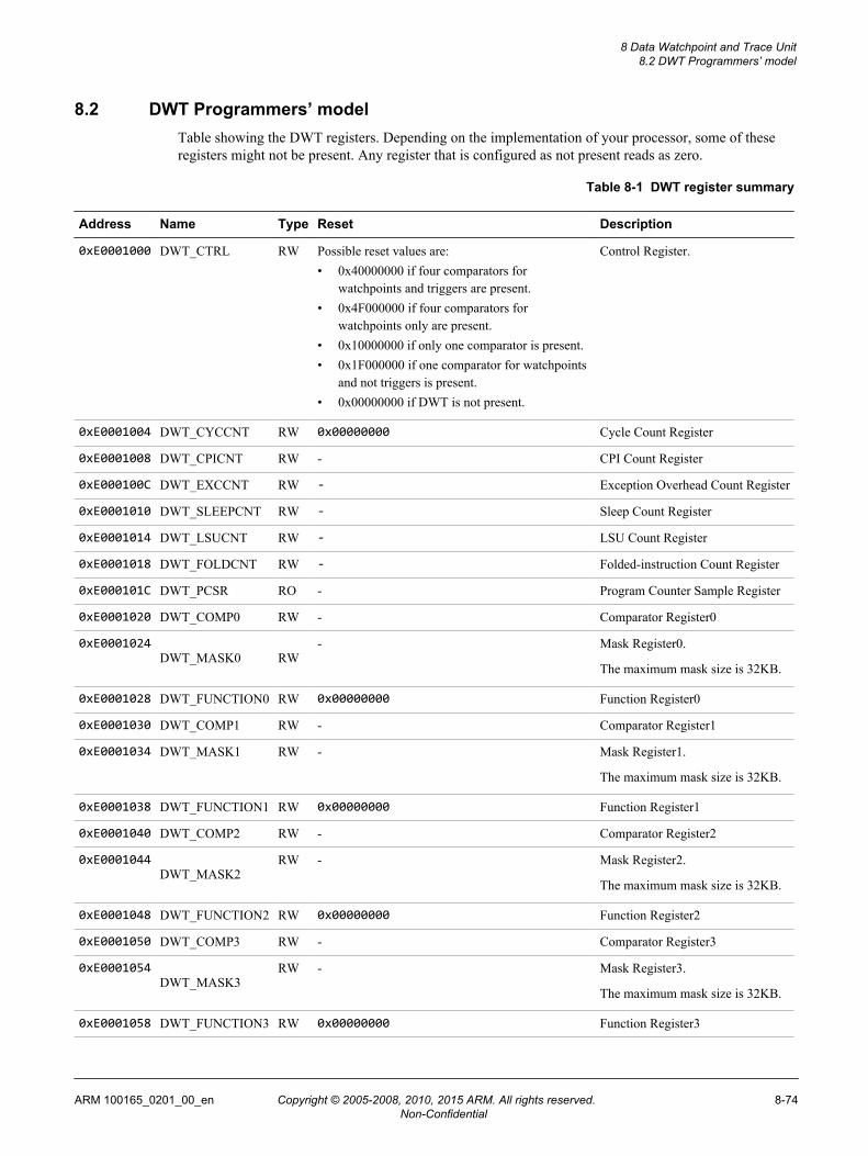
8.2 DWT Programmers’ modelTable showing the DWT registers. Depending on the implementation of your processor, some of theseregisters might not be present. Any register that is configured as not present reads as zero.
Table 8-1 DWT register summary
Address Name Type Reset Description
0xE0001000 DWT_CTRL RW Possible reset values are:• 0x40000000 if four comparators for
watchpoints and triggers are present.• 0x4F000000 if four comparators for
watchpoints only are present.• 0x10000000 if only one comparator is present.• 0x1F000000 if one comparator for watchpoints
and not triggers is present.• 0x00000000 if DWT is not present.
Control Register.
0xE0001004 DWT_CYCCNT RW 0x00000000 Cycle Count Register
0xE0001008 DWT_CPICNT RW - CPI Count Register
0xE000100C DWT_EXCCNT RW - Exception Overhead Count Register
0xE0001010 DWT_SLEEPCNT RW - Sleep Count Register
0xE0001014 DWT_LSUCNT RW - LSU Count Register
0xE0001018 DWT_FOLDCNT RW - Folded-instruction Count Register
0xE000101C DWT_PCSR RO - Program Counter Sample Register
0xE0001020 DWT_COMP0 RW - Comparator Register0
0xE0001024DWT_MASK0 RW
- Mask Register0.
The maximum mask size is 32KB.
0xE0001028 DWT_FUNCTION0 RW 0x00000000 Function Register0
0xE0001030 DWT_COMP1 RW - Comparator Register1
0xE0001034 DWT_MASK1 RW - Mask Register1.
The maximum mask size is 32KB.
0xE0001038 DWT_FUNCTION1 RW 0x00000000 Function Register1
0xE0001040 DWT_COMP2 RW - Comparator Register2
0xE0001044DWT_MASK2
RW - Mask Register2.
The maximum mask size is 32KB.
0xE0001048 DWT_FUNCTION2 RW 0x00000000 Function Register2
0xE0001050 DWT_COMP3 RW - Comparator Register3
0xE0001054DWT_MASK3
RW - Mask Register3.
The maximum mask size is 32KB.
0xE0001058 DWT_FUNCTION3 RW 0x00000000 Function Register3
8 Data Watchpoint and Trace Unit8.2 DWT Programmers’ model
ARM 100165_0201_00_en Copyright © 2005-2008, 2010, 2015 ARM. All rights reserved. 8-74Non-Confidential

Table 8-1 DWT register summary (continued)
Address Name Type Reset Description
0xE0001FD0 PID4 RO 0x04 Peripheral identification registers
0xE0001FD4 PID5 RO 0x00
0xE0001FD8 PID6 RO 0x00
0xE0001FDC PID7 RO 0x00
0xE0001FE0 PID0 RO 0x02
0xE0001FE4 PID1 RO 0xB0
0xE0001FE8 PID2 RO 0x3B
0xE0001FEC PID3 RO 0x00
0xE0001FF0 CID0 RO 0x0D Component identification registers
0xE0001FF4 CID1 RO 0xE0
0xE0001FF8 CID2 RO 0x05
0xE0001FFC CID3 RO 0xB1
DWT registers are described in the ARM®v7M Architecture Reference Manual. Peripheral Identificationand Component Identification registers are described in the ARM® CoreSight™ Components TechnicalReference Manual.
Note
• Cycle matching functionality is only available in comparator 0.• Data matching functionality is only available in comparator 1.• Data value is only sampled for accesses that do not produce an MPU or bus fault. The PC is sampled
irrespective of any faults. The PC is only sampled for the first address of a burst.• The FUNCTION field in the DWT_FUNCTION1 register is overridden for comparators given by
DATAVADDR0 and DATAVADDR1 if DATAVMATCH is also set in DWT_FUNCTION1. Thecomparators given by DATAVADDR0 and DATAVADDR1 can then only perform addresscomparator matches for comparator 1 data matches.
• If the data matching functionality is not included during implementation it is not possible to setDATAVADDR0, DATAVADDR1, or DATAVMATCH in DWT_FUNCTION1. This means that thedata matching functionality is not available in the implementation. Test the availability of datamatching by writing and reading the DATAVMATCH bit in DWT_FUNCTION1. If this bit cannotbe set then data matching is unavailable.
• ARM does not recommend PC match for watchpoints because it stops after the instruction. It mainlyguards and triggers the ETM.
8 Data Watchpoint and Trace Unit8.2 DWT Programmers’ model
ARM 100165_0201_00_en Copyright © 2005-2008, 2010, 2015 ARM. All rights reserved. 8-75Non-Confidential
Chapter 9Instrumentation Trace Macrocell Unit
This chapter describes the Instrumentation Trace Macrocell (ITM) unit.
It contains the following sections:• 9.1 ITM functional description on page 9-77.• 9.2 ITM programmers’ model on page 9-78.• 9.3 ITM Trace Privilege Register, ITM_TPR on page 9-79.
ARM 100165_0201_00_en Copyright © 2005-2008, 2010, 2015 ARM. All rights reserved. 9-76Non-Confidential

9.1 ITM functional descriptionThe ITM is a an optional application-driven trace source that supports printf() style debugging to traceoperating system and application events, and generates diagnostic system information. The ITMgenerates trace information as packets from software traces, hardware traces, time stamping, and globalsystem timestamping sources.
The ITM generates trace information as packets. There are four sources that can generate packets. Ifmultiple sources generate packets at the same time, the ITM arbitrates the order in which packets areoutput. The four sources in decreasing order of priority are:• Software trace. Software can write directly to ITM stimulus registers to generate packets.• Hardware trace. The DWT generates these packets, and the ITM outputs them.• Time stamping. Timestamps are generated relative to packets. The ITM contains a 21-bit counter to
generate the timestamp. The Cortex-M3 clock or the bitclock rate of the Serial Wire Viewer (SWV)output clocks the counter.
9 Instrumentation Trace Macrocell Unit9.1 ITM functional description
ARM 100165_0201_00_en Copyright © 2005-2008, 2010, 2015 ARM. All rights reserved. 9-77Non-Confidential
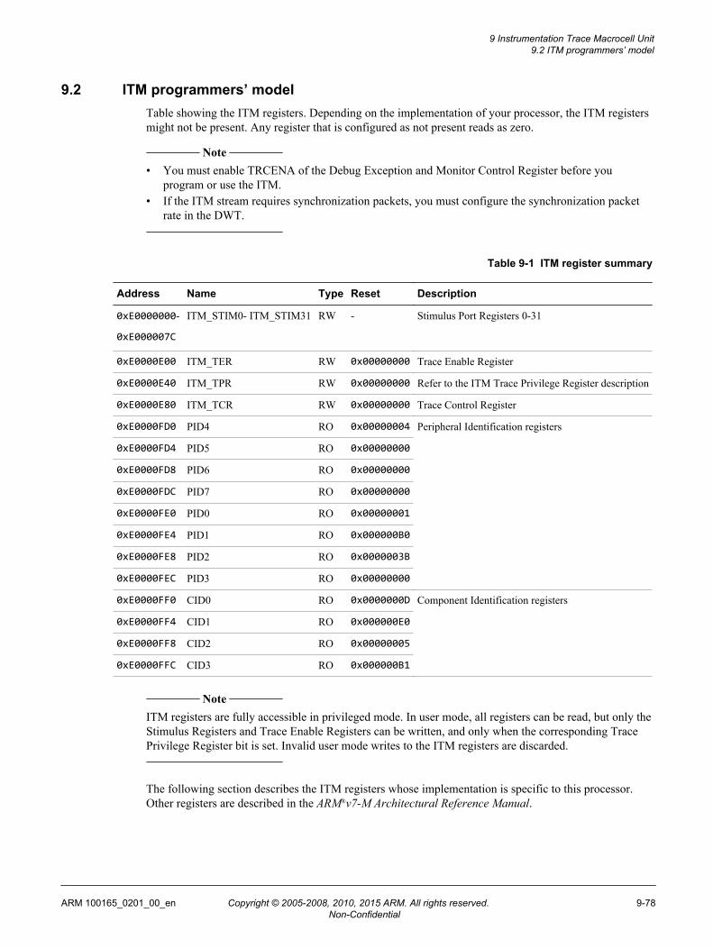
9.2 ITM programmers’ modelTable showing the ITM registers. Depending on the implementation of your processor, the ITM registersmight not be present. Any register that is configured as not present reads as zero.
Note
• You must enable TRCENA of the Debug Exception and Monitor Control Register before youprogram or use the ITM.
• If the ITM stream requires synchronization packets, you must configure the synchronization packetrate in the DWT.
Table 9-1 ITM register summary
Address Name Type Reset Description
0xE0000000-
0xE000007C
ITM_STIM0- ITM_STIM31 RW - Stimulus Port Registers 0-31
0xE0000E00 ITM_TER RW 0x00000000 Trace Enable Register
0xE0000E40 ITM_TPR RW 0x00000000 Refer to the ITM Trace Privilege Register description
0xE0000E80 ITM_TCR RW 0x00000000 Trace Control Register
0xE0000FD0 PID4 RO 0x00000004 Peripheral Identification registers
0xE0000FD4 PID5 RO 0x00000000
0xE0000FD8 PID6 RO 0x00000000
0xE0000FDC PID7 RO 0x00000000
0xE0000FE0 PID0 RO 0x00000001
0xE0000FE4 PID1 RO 0x000000B0
0xE0000FE8 PID2 RO 0x0000003B
0xE0000FEC PID3 RO 0x00000000
0xE0000FF0 CID0 RO 0x0000000D Component Identification registers
0xE0000FF4 CID1 RO 0x000000E0
0xE0000FF8 CID2 RO 0x00000005
0xE0000FFC CID3 RO 0x000000B1
Note
ITM registers are fully accessible in privileged mode. In user mode, all registers can be read, but only theStimulus Registers and Trace Enable Registers can be written, and only when the corresponding TracePrivilege Register bit is set. Invalid user mode writes to the ITM registers are discarded.
The following section describes the ITM registers whose implementation is specific to this processor.Other registers are described in the ARM®v7-M Architectural Reference Manual.
9 Instrumentation Trace Macrocell Unit9.2 ITM programmers’ model
ARM 100165_0201_00_en Copyright © 2005-2008, 2010, 2015 ARM. All rights reserved. 9-78Non-Confidential
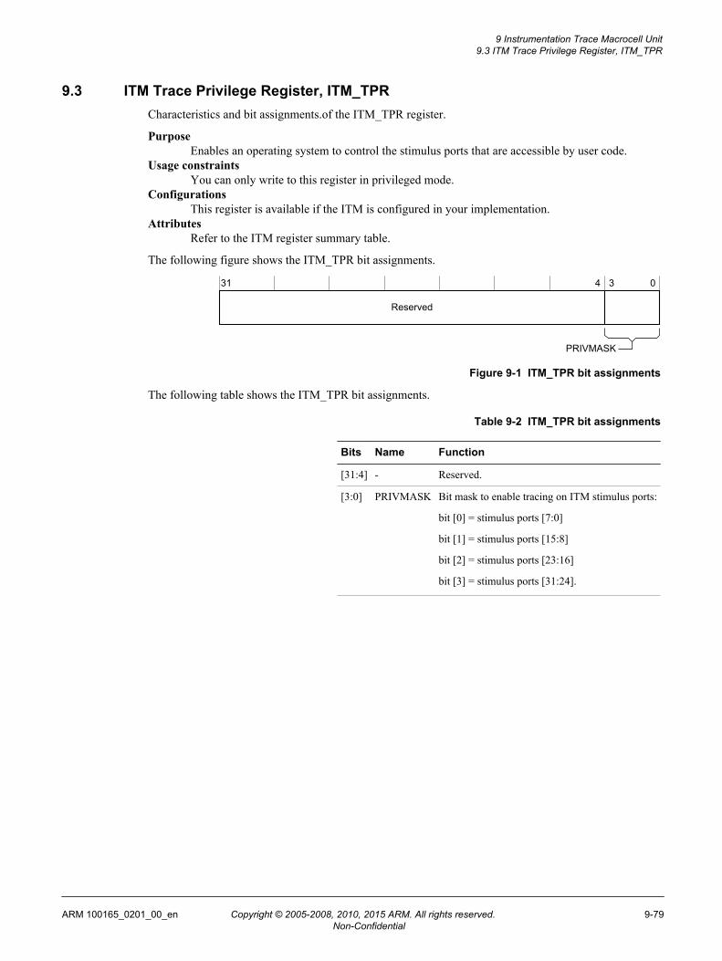
9.3 ITM Trace Privilege Register, ITM_TPRCharacteristics and bit assignments.of the ITM_TPR register.
PurposeEnables an operating system to control the stimulus ports that are accessible by user code.
Usage constraintsYou can only write to this register in privileged mode.
ConfigurationsThis register is available if the ITM is configured in your implementation.
AttributesRefer to the ITM register summary table.
The following figure shows the ITM_TPR bit assignments.
Reserved
31 4 3 0
PRIVMASK
Figure 9-1 ITM_TPR bit assignments
The following table shows the ITM_TPR bit assignments.
Table 9-2 ITM_TPR bit assignments
Bits Name Function
[31:4] - Reserved.
[3:0] PRIVMASK Bit mask to enable tracing on ITM stimulus ports:
bit [0] = stimulus ports [7:0]
bit [1] = stimulus ports [15:8]
bit [2] = stimulus ports [23:16]
bit [3] = stimulus ports [31:24].
9 Instrumentation Trace Macrocell Unit9.3 ITM Trace Privilege Register, ITM_TPR
ARM 100165_0201_00_en Copyright © 2005-2008, 2010, 2015 ARM. All rights reserved. 9-79Non-Confidential

Chapter 10Embedded Trace Macrocell
This chapter describes the Embedded Trace Macrocell (ETM).
It contains the following sections:• 10.1 About the ETM on page 10-81.• 10.2 ETM functional description on page 10-82.• 10.3 ETM Programmers model on page 10-88.
ARM 100165_0201_00_en Copyright © 2005-2008, 2010, 2015 ARM. All rights reserved. 10-80Non-Confidential

10.1 About the ETMThe ETM is an optional debug component that enables reconstruction of program execution. The ETM isdesigned to be a high-speed, low-power debug tool that only supports instruction trace. This ensures thatarea is minimized, and that gate count is reduced.
This section contains the following subsections:• 10.1.1 ETM architecture on page 10-81.• 10.1.2 ETM features list on page 10-81.• 10.1.3 Configurable options list on page 10-81.
10.1.1 ETM architecture
The ETM implements ARM ETM architecture v3.5.
The ETM traces all 32-bit Thumb instructions as a single instruction. The ETM traces instructionsfollowing an IT instruction as normal conditional instructions. The decompressor does not need to referto the IT instruction.
You can use the CoreSight ETM-M3 either with the Cortex-M3 Trace Port Interface Unit (M3-TPIU), oras part of a CoreSight system.
For more information, see the ARM® Embedded Trace Macrocell Architecture Specification.
10.1.2 ETM features list
List of features provided by the ETM component.
ETM-M3 provides:• Tracing of 16-bit and 32-bit Thumb instructions.• Four EmbeddedICE watchpoint inputs.• A Trace Start/Stop block with EmbeddedICE inputs.• Two external inputs.• A 24-byte FIFO queue.• Global timestamping.
See the Embedded Trace Macrocell Architecture Specification for information about:
• The trace protocol.• Controlling tracing using triggering and filtering resources.
See the Cortex®-M3 Integration and Implementation Manual for information about the macrocell signals.
10.1.3 Configurable options list
List of configuration inputs provided by the ETM component.
The ETM-M3 macrocell includes the following configuration inputs:• The maximum number of external inputs.• Whether the system supports the FIFOFULL mechanism for stalling the processor.
Related concepts10.2.7 External inputs on page 10-85.
10 Embedded Trace Macrocell10.1 About the ETM
ARM 100165_0201_00_en Copyright © 2005-2008, 2010, 2015 ARM. All rights reserved. 10-81Non-Confidential

10.2 ETM functional descriptionThe ETM receives input from the processor and outputs trace information to the TPIU or CoreSightsystem. ETM trace output is compatible with the AMBA Trace Bus (ATB) protocol.
This section contains the following subsections:• 10.2.1 ETM block diagram on page 10-82.• 10.2.2 Low-bandwidth data tracing on page 10-82.• 10.2.3 Resources on page 10-83.• 10.2.4 Timestamp format on page 10-85.• 10.2.5 Periodic synchronization on page 10-85.• 10.2.6 Data and instruction address compare resources on page 10-85.• 10.2.7 External inputs on page 10-85.• 10.2.8 Start/stop block on page 10-85.• 10.2.9 Triggering on page 10-86.• 10.2.10 Interfaces on page 10-86.• 10.2.11 Operation on page 10-87.
10.2.1 ETM block diagram
Block diagram of the ETM, showing how the ETM interfaces to the Trace Port Interface Unit (TPIU).
Cortex-M3 processor
DWT
ITMATB
ETM-M3
ATBCortex-M3
TPIU or Coresight systemCTI
Trace port and
SerialWire trace outputs
Trace Generation
Trace Control: Counter Start/Stop block Trigger generation Programming interface
Figure 10-1 ETM block diagram
10.2.2 Low-bandwidth data tracing
The Cortex-M3 system can perform low-bandwidth data tracing using the Data Watchpoint and Trace(DWT) and Instruction Trace Macrocell (ITM) components.
The ETM trace output is compatible with the AMBA Trace Bus (ATB) protocol, irrespective of theconfiguration of the trace port size and trace port mode within the ETM programmers model. The TPIUexports trace information from the processor. An implementation can replace the TPIU with otherCoreSight trace components.
The ETM provides a trace ID register for systems that use multiple trace sources. You must configurethis register even if only a single trace source is in use.
Related concepts10.2.5 Periodic synchronization on page 10-85.10.2.6 Data and instruction address compare resources on page 10-85.10.2.7 External inputs on page 10-85.10.2.8 Start/stop block on page 10-85.10.2.9 Triggering on page 10-86.10.2.10 Interfaces on page 10-86.10.2.11 Operation on page 10-87.
10 Embedded Trace Macrocell10.2 ETM functional description
ARM 100165_0201_00_en Copyright © 2005-2008, 2010, 2015 ARM. All rights reserved. 10-82Non-Confidential
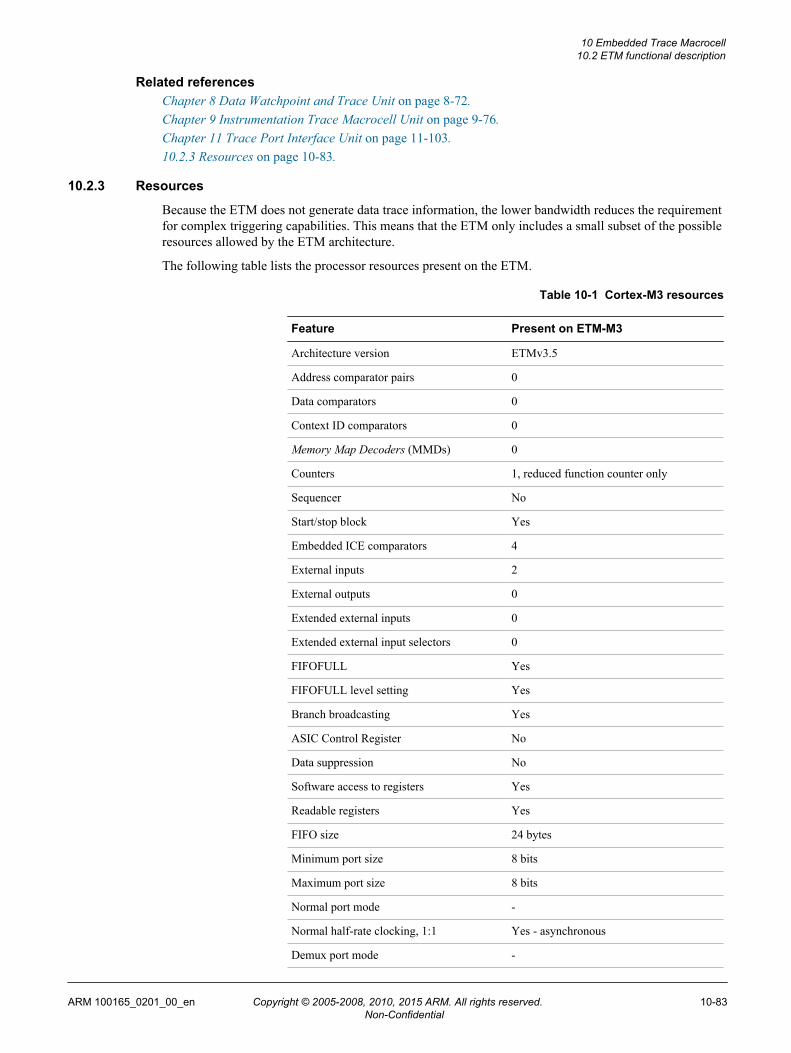
Related referencesChapter 8 Data Watchpoint and Trace Unit on page 8-72.Chapter 9 Instrumentation Trace Macrocell Unit on page 9-76.Chapter 11 Trace Port Interface Unit on page 11-103.10.2.3 Resources on page 10-83.
10.2.3 Resources
Because the ETM does not generate data trace information, the lower bandwidth reduces the requirementfor complex triggering capabilities. This means that the ETM only includes a small subset of the possibleresources allowed by the ETM architecture.
The following table lists the processor resources present on the ETM.
Table 10-1 Cortex-M3 resources
Feature Present on ETM-M3
Architecture version ETMv3.5
Address comparator pairs 0
Data comparators 0
Context ID comparators 0
Memory Map Decoders (MMDs) 0
Counters 1, reduced function counter only
Sequencer No
Start/stop block Yes
Embedded ICE comparators 4
External inputs 2
External outputs 0
Extended external inputs 0
Extended external input selectors 0
FIFOFULL Yes
FIFOFULL level setting Yes
Branch broadcasting Yes
ASIC Control Register No
Data suppression No
Software access to registers Yes
Readable registers Yes
FIFO size 24 bytes
Minimum port size 8 bits
Maximum port size 8 bits
Normal port mode -
Normal half-rate clocking, 1:1 Yes - asynchronous
Demux port mode -
10 Embedded Trace Macrocell10.2 ETM functional description
ARM 100165_0201_00_en Copyright © 2005-2008, 2010, 2015 ARM. All rights reserved. 10-83Non-Confidential
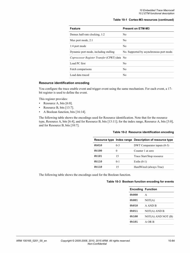
Table 10-1 Cortex-M3 resources (continued)
Feature Present on ETM-M3
Demux half-rate clocking, 1:2 No
Mux port mode, 2:1 No
1:4 port mode No
Dynamic port mode, including stalling No. Supported by asynchronous port mode.
Coprocessor Register Transfer (CPRT) data No
Load PC first No
Fetch comparisons No
Load data traced No
Resource identification encoding
You configure the trace enable event and trigger event using the same mechanism. For each event, a 17-bit register is used to define the event.
This register provides:• Resource A, bits [6:0].• Resource B, bits [13:7].• A Boolean function, bits [16:14].
The following table shows the encodings used for Resource identification. Note that for the resourcetype, Resource A, bits [6:4], and for Resource B, bits [13:11]; for the index range, Resource A, bits [3:0],and for Resource B, bits [10:7].
Table 10-2 Resource identification encoding
Resource type Index range Description of resource type
0b010 0-3 DWT Comparator inputs (0-3)
0b100 0 Counter 1 at zero
0b101 15 Trace Start/Stop resource
0b110 0-1 ExtIn (0-1)
0b110 15 HardWired (always True)
The following table shows the encodings used for the Boolean function.
Table 10-3 Boolean function encoding for events
Encoding Function
0b000 A
0b001 NOT(A)
0b010 A AND B
0b011 NOT(A) AND B
0b100 NOT(A) AND NOT (B)
0b101 A OR B
10 Embedded Trace Macrocell10.2 ETM functional description
ARM 100165_0201_00_en Copyright © 2005-2008, 2010, 2015 ARM. All rights reserved. 10-84Non-Confidential

Table 10-3 Boolean function encoding for events (continued)
Encoding Function
0b110 NOT (A) OR B
0b111 NOT (A) OR NOT (B)
10.2.4 Timestamp format
Timestamps are encoded as 48-bit natural binary numbers.
A system implementation may provide a timestamp count which can be used by several trace sources asan aid to correlating the trace streams.
10.2.5 Periodic synchronization
The ETM uses a fixed synchronization packet generation frequency of every 1024 bytes of trace.
10.2.6 Data and instruction address compare resources
The DWT provides four address comparators on the data bus that provide debug functionality.
Within the DWT unit, you can specify the functions triggered by a match, and one of these functions isto generate an ETM match input. These inputs are presented to the ETM as Embedded In CircuitEmulator (ICE) comparator inputs.
A single DWT resource can trigger an ETM event and also generate instrumentation trace directly fromthe same event.
You can configure the four DWT comparators individually to compare with the address of the currentexecuting instruction to permit the ETM access to an instruction address compare resource. These inputsare presented to the ETM as Embedded ICE comparator inputs. The DWT provides either one or fourcomparators, depending on the implementation of the processor.
Note
Using a DWT comparator as an instruction address comparator reduces the number of available dataaddress comparisons.
Related referencesChapter 8 Data Watchpoint and Trace Unit on page 8-72.
10.2.7 External inputs
Two external inputs, ETMEXTIN[1:0], enable additional components to generate trigger and enablesignals for the ETM.
10.2.8 Start/stop block
The start/stop block provides a single-bit resource that can be used as an input to other parts of theresource logic, including the trace enable logic.
The start/stop block can only be controlled by using the EmbeddedICE inputs to the ETM. The DWTcontrols these inputs.
The start/stop block is set to the start state if any of the EmbeddedICE watchpoint inputs selected as startresources in ETMTESSEICR go HIGH. The start/stop block is set to the stop state if any of theEmbeddedICE watchpoint inputs selected as stop resources in ETMTESSEICR go LOW.
If bit [25] of ETMTECR1 is 1, tracing will only be enabled when the start/stop block is in the start state.
10 Embedded Trace Macrocell10.2 ETM functional description
ARM 100165_0201_00_en Copyright © 2005-2008, 2010, 2015 ARM. All rights reserved. 10-85Non-Confidential

Tracing is also only enabled when the result of evaluating the Trace Enable Event is TRUE. This eventcan be set to always be TRUE by programming a value of 0x6F to ETMTEEVR. For more informationsee the Embedded Trace Macrocell Architecture Specification.
10.2.9 Triggering
The ETM provides a trigger resource that can be used to identify a point within a trace run.
The generation of a trigger does not affect the tracing in any way, but the trigger will be output in thetrace stream, and can also be passed to other trace components or used to halt the processor. An externaltrace port analyzer can use the trigger to determine when to start and stop capture of trace.
10.2.10 Interfaces
The ETM provides three external interfaces which provide a trace output from the macrocell, a controlinterface for the macrocell, and an interface to manage the interconnection of trigger and control signalsbetween the processor core, ETM, and TPIU.
The ETM-M3 has the following external interfaces:
ATBA 32-bit Advanced Trace Bus provides trace output from the macrocell. See the AMBA 3 ATBProtocol Specification for more information about this interface.
APBAn Advanced Peripheral Bus provides the control interface for the macrocell. See the AMBA 3APB Protocol Specification for more information about this interface.
CTIYour implementation can provide a Cross Trigger Interface to manage the interconnection oftrigger and control signals between the processor core, ETM, and TPIU. The implementation ofyour Cortex-M3 processor determines which ETM functions are visible to the CTI.
Table of recommended CTI connections
Tables showing the recommended CTI connections for Cortex-M3 systems.
Note
These tables show the ARM standard connections, but the actual connections are implementation-defined. Refer to documentation from the supplier of your device for any changes to these connections.
Table 10-4 Input connections
Trigger bit Source signal Source device Comments
[7] ETMTRIGOUT ETM Recommended if ETM is present.
[6] ETMTRIGGER[2] DWT Recommended.
[5] ETMTRIGGER[1] DWT Recommended.
[4] ETMTRIGGER[0] DWT Recommended.
[3] ACQCOMP ETB Recommended if an Embedded Trace Buffer (ETB) is present. If multiple coresshare a single ETB, you must only connect to the CTI of one of the cores.
[2] FULL ETB
[1] User Defined - -
[0] HALTED Core Compulsory.
10 Embedded Trace Macrocell10.2 ETM functional description
ARM 100165_0201_00_en Copyright © 2005-2008, 2010, 2015 ARM. All rights reserved. 10-86Non-Confidential

Table 10-5 Trigger output connections
Trigger bit Destination signal Destination device Comments
[7] User defined - -
[6] User defined - -
[5] ETMEXTIN[1] ETM Compulsory if ETM is present.
[4] ETMEXTIN[0] ETM Compulsory if ETM is present.
[3] INTISR[y] NVIC Recommended if an ETB is present. If multiple cores share a single ETB,you must only connect to the CTI of one of the cores.
[2] INTISR[x] NVIC Compulsory. Any interrupt can be used.
[1] User defined - -
[0] EDBGRQ Core Compulsory.
10.2.11 Operation
ETM-M3 implements version 3.5 of the ARM Embedded Trace Macrocell protocol.
10 Embedded Trace Macrocell10.2 ETM functional description
ARM 100165_0201_00_en Copyright © 2005-2008, 2010, 2015 ARM. All rights reserved. 10-87Non-Confidential

10.3 ETM Programmers modelThe ETM programmers model provides mechanisms for programming the registers used to set up thetrace and triggering facilities of the macrocell.
This section contains the following subsections:• 10.3.1 Modes of operation and execution on page 10-88.• 10.3.2 ETM register summary table on page 10-88.• 10.3.3 Main Control Register, ETMCR on page 10-90.• 10.3.4 Configuration Code Register, ETMCCR on page 10-93.• 10.3.5 System Configuration Register, ETMSCR on page 10-94.• 10.3.6 TraceEnable Control 1 Register, ETMTECR1 characteristics on page 10-95.• 10.3.7 ID Register, ETMIDR characteristics on page 10-95.• 10.3.8 Configuration Code Extension Register, ETMCCER characteristics on page 10-96.• 10.3.9 TraceEnable Start/Stop EmbeddedICE Control Register, ETMTESSEICR on page 10-98.• 10.3.10 Device Power-Down Status Register, ETMPDSR on page 10-99.• 10.3.11 Integration Test Miscellaneous Inputs, ITMISCIN on page 10-99.• 10.3.12 Integration Test Trigger Out, ITTRIGOUT on page 10-100.• 10.3.13 ETM Integration Test ATB Control 2, ETM_ITATBCTR2 on page 10-101.• 10.3.14 ETM Integration Test ATB Control 0, ETM_ITATBCTR0 on page 10-101.
10.3.1 Modes of operation and execution
On power-up or reset of the ETM you must program all registers which do not have an architected resetstate before enabling tracing, and enable all register changes at the same time using the Programming bitin ETMCR.
ETM-M3 implements ETMv3.5 for tracing 16-bit and 32-bit Thumb instructions. The Embedded TraceMacrocell Architecture Specification describes the features of ETMv3.5.
When the ETM is powered up or reset, you must program all of the registers that do not have anarchitected reset state before you enable tracing. If you do not do so, the trace results are Unpredictable.
When programming the ETM registers you must enable all the changes at the same time. To achieve this,use the Programming bit in ETMCR.
When the Programming bit is set to 0 you must not write to registers other than ETMCR, because thiscan lead to Unpredictable behavior.
When setting the Programming bit, you must not change any other bits of ETMCR. You must onlychange the value of bits other than the Programming bit of ETMCR when bit [1] of ETMSR is set to 1.ARM recommends that you use a read-modify-write procedure when changing ETMCR.
Related references10.1.2 ETM features list on page 10-81.10.3.3 Main Control Register, ETMCR on page 10-90.
10.3.2 ETM register summary table
Table of ETM registers with register address, name, reset, type, and description information.
Table 10-6 ETM registers
Address Name Reset Type Description
0xE0041000 ETMCR 0x00000411 RW Main Control Register, ETMCR
0xE0041004 ETMCCR 0x8C802000 RO Configuration Code Register, ETMCCR
10 Embedded Trace Macrocell10.3 ETM Programmers model
ARM 100165_0201_00_en Copyright © 2005-2008, 2010, 2015 ARM. All rights reserved. 10-88Non-Confidential

Table 10-6 ETM registers (continued)
Address Name Reset Type Description
0xE0041008 ETMTRIGGER - RW Trigger Event Register. See ARM® Embedded Trace MacrocellArchitecture Specification
0xE0041010 ETMSR - RW ETM Status Register. See ARM® Embedded Trace MacrocellArchitecture Specification
0xE0041014 ETMSCR 0x00020D09 RO System Configuration Register, ETMSCR
0xE0041020 ETMTEEVR - RW TraceEnable Event Register. See ARM® Embedded Trace MacrocellArchitecture Specification
0xE0041024 ETMTECR1 - RW TraceEnable Control 1 Register, ETMTECR1
0xE0041028 ETMFFLR - RW FIFOFULL Level Register. See ARM® Embedded Trace MacrocellArchitecture Specification
0xE0041140 ETMCNTRLDVR1 - RW Free-running counter reload value
0xE00411E0 ETMSYNCFR 0x00000400 RO Synchronisation Frequency Register. See ARM® Embedded TraceMacrocell Architecture Specification
0xE00411E4 ETMIDR 0x4114F253 RO ID Register, ETMIDR
0xE00411E8 ETMCCER 0x18541800 RO Configuration Code Extension Register, ETMCCER
0xE00411F0 ETMTESSEICR - RW TraceEnable Start/Stop EmbeddedICE Control Register,ETMTESSEICR
0xE00411F8 ETMTSEVR - RW Timestamp Event Register. See ARM® Embedded Trace MacrocellArchitecture Specification
0xE0041200 ETMTRACEIDR 0x00000000 RW CoreSight Trace ID Register. See ARM® Embedded Trace MacrocellArchitecture Specification
0xE0041208 ETMIDR2 0x00000000 RO ETM ID Register 2. See ARM® Embedded Trace Macrocell ArchitectureSpecification
0xE0041314 ETMPDSR 0x00000001 RO Device Power-Down Status Register, ETMPDSR
0xE0041EE0 ITMISCIN - RO Integration Test Miscellaneous Inputs, ITMISCIN
0xE0041EE8 ITTRIGOUT - WO Integration Test Trigger Out, ITTRIGOUT
0xE0041EF0 ETM_ITATBCTR2 - RO ETM Integration Test ATB Control 2, ETM_ITATBCTR2
0xE0041EF8 ETM_ITATBCTR0 - WO ETM Integration Test ATB Control 0, ETM_ITATBCTR0
0xE0041F00 ETMITCTRL 0x00000000 RW Integration Mode Control Register. See ARM® Embedded TraceMacrocell Architecture Specification
0xE0041FA0 ETMCLAIMSET - RW Claim Tag Set Register. See ARM® Embedded Trace MacrocellArchitecture Specification
0xE0041FA4 ETMCLAIMCLR - RW Claim Tag Clear Register. See ARM® Embedded Trace MacrocellArchitecture Specification
0xE0041FB0 ETMLAR - RW Lock Access Register. See ARM® Embedded Trace MacrocellArchitecture Specification
0xE0041FB4 ETMLSR - RO Lock Status Register. See ARM® Embedded Trace MacrocellArchitecture Specification
0xE0041FB8 ETMAUTHSTATUS - RO Authentication Status Register. See ARM® Embedded Trace MacrocellArchitecture Specification
10 Embedded Trace Macrocell10.3 ETM Programmers model
ARM 100165_0201_00_en Copyright © 2005-2008, 2010, 2015 ARM. All rights reserved. 10-89Non-Confidential
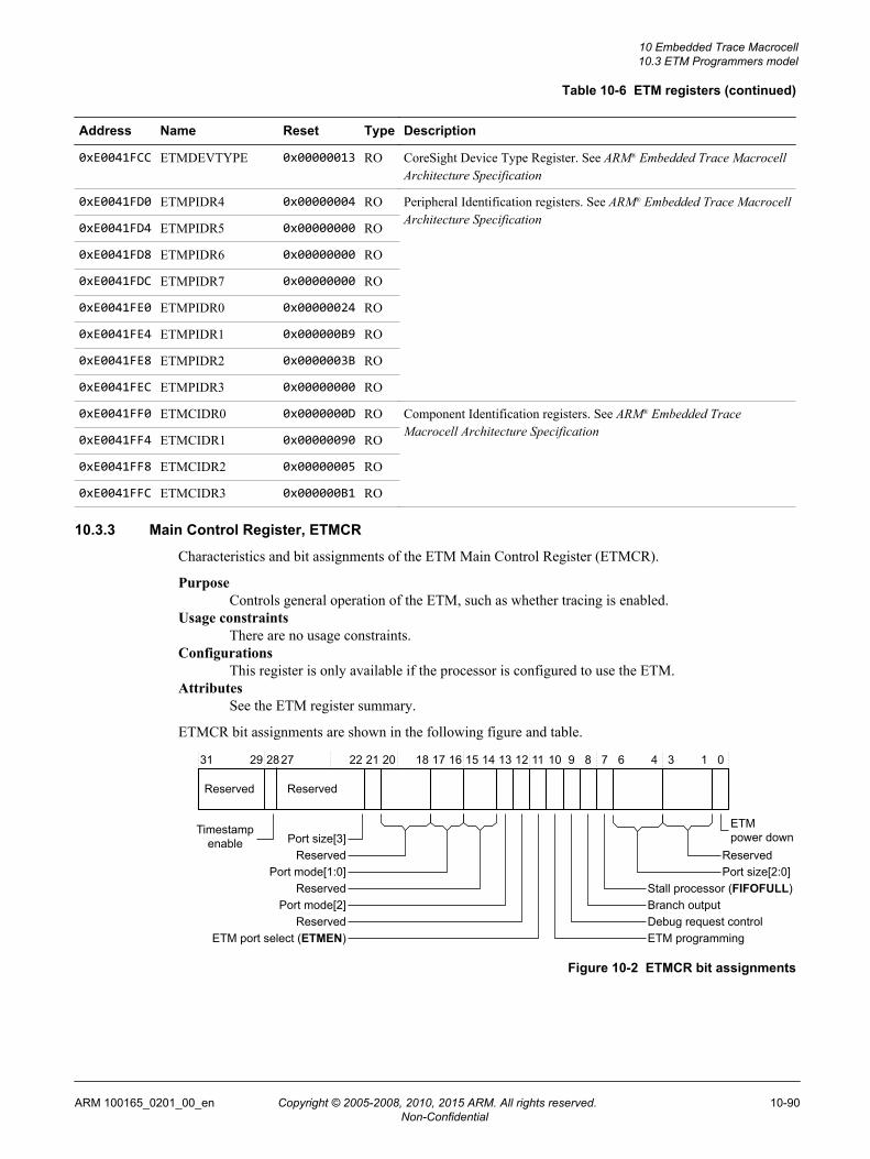
Table 10-6 ETM registers (continued)
Address Name Reset Type Description
0xE0041FCC ETMDEVTYPE 0x00000013 RO CoreSight Device Type Register. See ARM® Embedded Trace MacrocellArchitecture Specification
0xE0041FD0 ETMPIDR4 0x00000004 RO Peripheral Identification registers. See ARM® Embedded Trace MacrocellArchitecture Specification
0xE0041FD4 ETMPIDR5 0x00000000 RO
0xE0041FD8 ETMPIDR6 0x00000000 RO
0xE0041FDC ETMPIDR7 0x00000000 RO
0xE0041FE0 ETMPIDR0 0x00000024 RO
0xE0041FE4 ETMPIDR1 0x000000B9 RO
0xE0041FE8 ETMPIDR2 0x0000003B RO
0xE0041FEC ETMPIDR3 0x00000000 RO
0xE0041FF0 ETMCIDR0 0x0000000D RO Component Identification registers. See ARM® Embedded TraceMacrocell Architecture Specification
0xE0041FF4 ETMCIDR1 0x00000090 RO
0xE0041FF8 ETMCIDR2 0x00000005 RO
0xE0041FFC ETMCIDR3 0x000000B1 RO
10.3.3 Main Control Register, ETMCR
Characteristics and bit assignments of the ETM Main Control Register (ETMCR).
PurposeControls general operation of the ETM, such as whether tracing is enabled.
Usage constraintsThere are no usage constraints.
ConfigurationsThis register is only available if the processor is configured to use the ETM.
AttributesSee the ETM register summary.
ETMCR bit assignments are shown in the following figure and table.
31 22 20 17 16 15 13 12 8 7 4 3 0
Port size[3]
21
ReservedPort mode[1:0]
18
Port mode[2]
ETM port select (ETMEN) ETM programmingDebug request controlBranch outputStall processor (FIFOFULL)
ETMpower down
19 6
Port size[2:0]
14 11 10
Reserved
Reserved
Reserved
Timestamp enable
28
ReservedReserved
29 27
Figure 10-2 ETMCR bit assignments
10 Embedded Trace Macrocell10.3 ETM Programmers model
ARM 100165_0201_00_en Copyright © 2005-2008, 2010, 2015 ARM. All rights reserved. 10-90Non-Confidential

Table 10-7 ETMCR bit assignments
Bits Name Function
[31:29] - RAZ
[28] Timestamp enable When set, this bit enables timestamping.
An ETM reset sets this bit to 0.
[27:22] - Reserved
[21] Port size[3] This bit is implemented but has no function.
An ETM reset sets this bit to 0.
[20:18] - Reserved
[17:16] Port mode [1:0] These bits are implemented but have no function.
An ETM reset sets these bits to 0.
[15:14] - Reserved
[13] Port mode[2] This bit is implemented but has no function.
An ETM reset sets this bit to 0.
[12] - Reserved
[11] ETM port selection This bit can be used to control other trace components in an implementation. The possible values are:
0ETMEN is LOW.
1ETMEN is HIGH.
This bit must be set by the trace software tools to ensure that trace output is enabled from this ETM.
An ETM reset sets this bit to 0.
[10] ETM programming This bit must be set to 1 at the start of the ETM programming sequence. Tracing is prevented while thisbit is set to 1.
On an ETM reset this bit is set to 0b1.
[9] Debug requestcontrol
When set to 1 and the trigger event occurs, the DBGRQ output is asserted until DBGACK is observed.This enables the ARM processor to be forced into Debug state.
An ETM reset sets this bit to 0.
[8] Branch output When set to 1 all branch addresses are output, even if the branch was because of a direct branchinstruction. Setting this bit enables reconstruction of the program flow without having access to thememory image of the code being executed.
When this bit is set to 1, more trace data is generated, and this may affect the performance of the tracesystem. Information about the execution of a branch is traced regardless of the state of this bit.
An ETM reset sets this bit to 0.
10 Embedded Trace Macrocell10.3 ETM Programmers model
ARM 100165_0201_00_en Copyright © 2005-2008, 2010, 2015 ARM. All rights reserved. 10-91Non-Confidential

Table 10-7 ETMCR bit assignments (continued)
Bits Name Function
[7] Stall processor The FIFOFULL output can be used to stall the processor to prevent overflow. The FIFOFULL outputis only enabled when the stall processor bit is set to 1. When the bit is 0 the FIFOFULL output remainsLOW at all times and the FIFO overflows if there are too many trace packets. Trace resumes withoutcorruption after the FIFO has drained, if overflow does occur.
An ETM reset sets this bit to 0.
For information about the interaction of this bit with the ETMFFLR register see the Embedded TraceMacrocell Architecture Specification.
[6:4] Port size [2:0] The ETM-M3 has no influence over the external pins used for trace. These bits are implemented but notused.
On an ETM reset these bits reset to 0b001.
[3:1] - Reserved
[0] ETM power down This bit can be used by an implementation to control whether the ETM is in a low power state. This bitmust be cleared by the trace software tools at the beginning of a debug session.
When this bit is set to 1, writes to some registers and fields might be ignored. You can always write tothe following registers and fields:
• ETMCR bit [0].• ETMLAR.• ETMCLAIMSET register.• ETMCLAIMCLR register.
When the ETMCR is written with this bit set to 1, bits other than bit [0] might be ignored.
On an ETM reset this bit is set to 1.
10 Embedded Trace Macrocell10.3 ETM Programmers model
ARM 100165_0201_00_en Copyright © 2005-2008, 2010, 2015 ARM. All rights reserved. 10-92Non-Confidential

10.3.4 Configuration Code Register, ETMCCR
Characteristics and bit assignments of the Configuration Code Register (ETMCCR).
The ETMCCR characteristics are:
PurposeEnables software to read the implementation-specific configuration of the ETM.
Usage constraintsThere are no usage constraints.
ConfigurationsThis register is only available if the processor is configured to use the ETM.
AttributesRefer to the ETM register summary table.
ETMCCR bit assignments are shown in the following figure and table.
31 28 27 26 25 24 23 22 20 19 17 16 15 13 12 8 7 4 3 0
Coprocessor and memory mapped
access supported Number of counters
Reserved Number of data value comparators
Number of address comparator pairs
Number of memory map decoders
Sequencer presentNumber of external inputsNumber of external outputsFIFOFULL logic present
Trace start/stop block present
Number of Context IDcomparators
ETM ID register present
30
Figure 10-3 ETMCCR bit assignments
Table 10-8 ETMCCR bit assignments
Bits Name Function
[31] ETM ID register present The value of this bit is 1, indicating that the ETMIDR, register 0x79, is present and definesthe ETM architecture version in use.
[30:28] - Reserved.
[27] Coprocessor and memory access The value of this bit is 1, indicating that memory-mapped access to registers is supported.
[26] Trace start/stop block present The value of this bit is 1, indicating that the Trace start/stop block is present.
[25:24] Number of Context IDcomparators
The value of these bits is 0b00, indicating that Context ID comparators are notimplemented.
[23] FIFOFULL logic present The value of this bit is 1, indicating that FIFOFULL logic is present in the ETM. To useFIFOFULL the system must also support the function, as indicated by bit [8] of ETMSCR.
[22:20] Number of external outputs The value of these bits is 0b000, indicating that no external outputs are supported.
[19:17] Number of external inputs The value of these bits is between 0b000 and 0b010, indicating the number of externalinputs, from 0 to 2, implemented in the system.
[16] Sequencer present The value of this bit is 0, indicating that the sequencer is not implemented.
[15:13] Number of counters The value of these bits is 0b001, indicating that one counter is implemented.
[12:8] Number of memory mapdecoders
The value of these bits is 0b00000, indicating that memory map decoder inputs are notimplemented.
10 Embedded Trace Macrocell10.3 ETM Programmers model
ARM 100165_0201_00_en Copyright © 2005-2008, 2010, 2015 ARM. All rights reserved. 10-93Non-Confidential

Table 10-8 ETMCCR bit assignments (continued)
Bits Name Function
[7:4] Number of data valuecomparators
The value of these bits is 0b0000, indicating that data value comparators are notimplemented.
[3:0] Number of address comparatorpairs
The value of these bits is 0b0000, indicating that address comparator pairs are notimplemented.
10.3.5 System Configuration Register, ETMSCR
Characteristics and bit assignments of the System Configuration Register (ETMSCR).
The ETMSCR characteristics are:
PurposeShows the ETM features supported by the implementation of the ETM macrocell.
Usage constraintsThere are no usage constraints.
ConfigurationsThis register is only available if the processor is configured to use the ETM.
AttributesRefer to the ETM register summary table.
ETMSCR bit assignments are shown in the following figure and table.
No fetch comparisonsMaximum port size[2:0]
31 17 16 15 12 8 7 4 3 0
Reserved
18 14 11 10 9 2
Reserved, reads as 1Reserved, reads as 0x0
Reserved(N -1), where N = Number of supported processors
Port mode supportedPort size supported
Maximum port size[3]FIFOFULL supported
Figure 10-4 ETMSCR bit assignments
Table 10-9 ETMSCR bit assignments
Bits Name Function
[31:18] - Reserved.
[17] No Fetch comparisons The value of this bit is 1, indicating that fetch comparisons are not implemented.
[16:15] - Reserved.
[14:12] (N-1) These bits give the number of supported processors minus 1. The value of these bits is 0b000,indicating that there is only one processor connected.
[11] Port mode supported This bit reads as 1 if the currently selected port mode is supported. This has no effect on the TPIUtrace port.
[10] Port size supported This bit reads as 1 if the currently selected port size is supported. This has no effect on the TPIUtrace port.
[9] Maximum port size [3] Maximum ETM port size bit [3]. This bit is used in conjunction with bits [2:0]. Its value is 0. Thishas no effect on the TPIU trace port.
10 Embedded Trace Macrocell10.3 ETM Programmers model
ARM 100165_0201_00_en Copyright © 2005-2008, 2010, 2015 ARM. All rights reserved. 10-94Non-Confidential

Table 10-9 ETMSCR bit assignments (continued)
Bits Name Function
[8] FIFOFULL supported The value of this bit is 1, indicating that FIFOFULL is supported. This bit is used in conjunctionwith bit [23] of the ETMCCR.
[7:4] - Reserved, Read-As-Zero.
[3] - Reserved, Read-As-One.
[2:0] Maximum port size [2:0] Maximum ETM port size bits [2:0]. These bits are used in conjunction with bit [9]. The value ofthese bits is 0b001.
10.3.6 TraceEnable Control 1 Register, ETMTECR1 characteristics
Characteristics and bit assignments of the TraceEnable Control 1 Register (ETMTECR1).
The ETMTECR1 characteristics are:
PurposeEnables the start/stop logic used for trace enable.
Usage constraintsThere are no usage constraints.
ConfigurationsThis register is only available if the processor is configured to use the ETM.
AttributesRefer to the ETM register summary table.
ETMTECR1 bit assignments are shown in the following figure and table.
Reserved
31 0
Reserved
26 25 24
Trace control enable
Figure 10-5 ETMTECR1 bit assignments
Table 10-10 ETMTECR1 bit assignments
Bits Name Function
[31:26] - Reserved.
[25] Trace controlenable
Trace start/stop enable. The possible values of this bit are:
0Tracing is unaffected by the trace start/stop logic.
1Tracing is controlled by the trace on and off addresses configured for the trace start/stop logic.
The trace start/stop resource, resource 0x5F, is unaffected by the value of this bit.
[24:0] - Reserved.
10.3.7 ID Register, ETMIDR characteristics
Characteristics and bit assignments of the ID Register (ETMIDR).
The ETMIDR characteristics are:
PurposeHolds the ETM architecture variant, and defines the programmers model for the ETM.
10 Embedded Trace Macrocell10.3 ETM Programmers model
ARM 100165_0201_00_en Copyright © 2005-2008, 2010, 2015 ARM. All rights reserved. 10-95Non-Confidential

Usage constraintsThere are no usage constraints.
ConfigurationsThis register is only available if the processor is configured to use the ETM.
AttributesRefer to the ETM register summary table.
ETMIDR bit assignments are shown in the following figure and table.
Implementor code
Support for Security Extensions
31 17 16 15 12 8 7 4 3 018 11
ETM architecture version number
Load PC first
24 23 20 19
Major Minor
Implementation revision
Processor family
21
ReservedSupport for 32-bit Thumb instructions
Implements alternative branch packet encoding
Reserved
Figure 10-6 ETMIDR bit assignments
Table 10-11 ETMIDR bit assignments
Bits Name Function
[31:24] Implementer code These bits identify ARM as the implementer of the processor. The value of these bits is0b01000001.
[23:21] - Reserved.
[20] Branch packet encoding The value of this bit is 1, indicating that alternative branch packet encoding isimplemented.
[19] Security Extensions support The value of this bit is 0, indicating that the ETM behaves as if the processor is in Securestate at all times.
[18] 32-bit Thumb instruction tracing The value of this bit is 1, indicating that a 32-bit Thumb instruction is traced as a singleinstruction.
[17] - Reserved.
[16] Load PC first The value of this bit is 0, indicating that data tracing is not supported.
[15:12] Processor family The value of these bits is 0b1111, indicating that the processor family is not identified inthis register.
[11:8] Major ETM architecture version The value of these bits is 0b0010, indicating major architecture version number 3, ETMv3.
[7:4] Minor ETM architecture version The value of these bits is 0b0101, indicating minor architecture version number 5.
[3:0] Implementation revision The value of these bits is 0b0011, indicating implementation revision, 3.
10.3.8 Configuration Code Extension Register, ETMCCER characteristics
Characteristics and bit assignments of the Configuration Code Extension Register (ETMCCER).
The ETMCCER characteristics are:
PurposeHolds ETM configuration information additional to that in the ETMCCR.
Usage constraintsThere are no usage constraints.
ConfigurationsThis register is only available if the processor is configured to use the ETM.
10 Embedded Trace Macrocell10.3 ETM Programmers model
ARM 100165_0201_00_en Copyright © 2005-2008, 2010, 2015 ARM. All rights reserved. 10-96Non-Confidential

AttributesRefer to the ETM register summary table.
ETMCCER bit assignments are shown in the following figure and table.
Extended externalinput bus size
Number of extended external input selectors
Data address comparison supportedNumber of
Instrumentation resources
All registers readable
Number of EmbeddedICE watchpoint inputs
Trace Start/Stop block usesEmbeddedICE inputs
ETMEIBCR implemented
31 29 28 27 26 23 22 21 20 19 16 15 13 12 11 10 2 03
Timestamping implemented
Reserved
Reduced function counter
Timestamp encoding
30
Timestamp sizeReserved
Figure 10-7 ETMCCER bit assignments
Table 10-12 ETMCCER bit assignments
Bits Name Function
[31:30] - Reserved. Read-As-Zero.
[29] Timestamp size Set to 0 to indicate a size of 48 bits.
[28] Timestamp encoding Set to 1 to indicate that the timestamp is encoded as a natural binary number.
10 Embedded Trace Macrocell10.3 ETM Programmers model
ARM 100165_0201_00_en Copyright © 2005-2008, 2010, 2015 ARM. All rights reserved. 10-97Non-Confidential

Table 10-12 ETMCCER bit assignments (continued)
Bits Name Function
[27] Reduced function counter Set to 1 to indicate that Counter 1 is a reduced function counter.
[26:23] - Reserved, Read-As-Zero.
[22] Timestamping implemented This bit is set to 1, indicating that timestamping is implemented.
[21] EmbeddedICE behavior controlimplemented
The value of this bit is 0, indicating that the ETMEIBCR is not implemented. For moreinformation on EmbeddedICE behavior see the Embedded Trace Macrocell ArchitectureSpecification.
[20] Trace Start/Stop block usesEmbeddedICE watchpoint inputs
The value of this bit is 1, indicating that the Trace Start/Stop block uses the EmbeddedICEwatchpoint inputs.
[19:16] EmbeddedICE watchpoint inputs The value of these bits is 0b0100, indicating that the number of EmbeddedICEwatchpoint inputs implemented is four. These inputs come from the DWT.
[15:13] Instrumentation resources The value of these bits is 0b000, indicating that no Instrumentation resources aresupported.
[12] Data address comparisons The value of this bit is 1, indicating that data address comparisons are not supported.
[11] Readable registers The value of this bit is 1, indicating that all registers are readable.
[10:3] Extended external input bus The value of these bits is 0, indicating that the extended external input bus is notimplemented.
[2:0] Extended external input selectors The value of these bits is 0, indicating that extended external input selectors are notimplemented.
10.3.9 TraceEnable Start/Stop EmbeddedICE Control Register, ETMTESSEICR
Characteristics and bit assignments of the TraceEnable Start/Stop EmbeddedICE Control Register(ETMTESSEICR).
The ETMTESSEICR characteristics are:
PurposeSpecifies the EmbeddedICE watchpoint comparator inputs that are used to control the start/stopresource.
Usage constraintsThere are no usage constraints.
ConfigurationsThis register is only available if the processor is configured to use the ETM.
AttributesRefer to the ETM register summary table.
ETMTESSEICR bit assignments are shown in the following figure and table.
Reserved, RAZ
31 16 15 0
Reserved, RAZ
4 3 2 1 4 3 2 1
19 4 3
Start resource select bitsStop resource select bits
20 18 17 2 1
Figure 10-8 ETMTESSEICR bit assignments
10 Embedded Trace Macrocell10.3 ETM Programmers model
ARM 100165_0201_00_en Copyright © 2005-2008, 2010, 2015 ARM. All rights reserved. 10-98Non-Confidential

Table 10-13 ETMTESSEICR bit assignments
Bits Name Function
[31:20] - Reserved, Read-as-zero.
[19:16] Stop resourceselection
Setting any of these bits to 1 selects the corresponding EmbeddedICE watchpoint input as aTraceEnable stop resource. Bit [16] corresponds to input 1, bit [17] corresponds to input 2, bit [18]corresponds to input 3, and bit [19] corresponds to input 4.
[15:4] - Reserved, Read-As-Zero.
[3:0] Start resourceselection
Setting any of these bits to 1 selects the corresponding EmbeddedICE watchpoint input as aTraceEnable start resource. Bit [0] corresponds to input 1, bit [1] corresponds to input 2, bit [2]corresponds to input 3, and bit [3] corresponds to input 4.
10.3.10 Device Power-Down Status Register, ETMPDSR
Characteristics and bit assignments of the Device Power-Down Status Register (ETMPDSR).
The ETMPDSR characteristics are:
PurposeIndicates the power-down status of the ETM.
Usage constraintsThere are no usage constraints.
ConfigurationsThis register is only available if the processor is configured to use an ETM.
AttributesRefer to the ETM register summary table.
ETMPDSR bit assignments are shown in the following figure and table.
Reserved, RAZ
31 01
ETM powered up
Figure 10-9 ETMPDSR bit assignments
Table 10-14 ETMPDSR bit assignments
Bits Name Function
[31:1] - Reserved, Read-As-Zero.
[0] ETM powered up The value of this bit indicates whether you can access the ETM Trace Registers. The value of this bit isalways 1, indicating that the ETM Trace Registers can be accessed.
10.3.11 Integration Test Miscellaneous Inputs, ITMISCIN
Characteristics and bit assignments of the Integration Test Miscellaneous Inputs (ITMISCIN) register.
The ITMISCIN characteristics are:
PurposeIntegration test.
Usage constraintsThere are no usage constraints.
ConfigurationsThis register is only available if the processor is configured to use the ETM.
10 Embedded Trace Macrocell10.3 ETM Programmers model
ARM 100165_0201_00_en Copyright © 2005-2008, 2010, 2015 ARM. All rights reserved. 10-99Non-Confidential
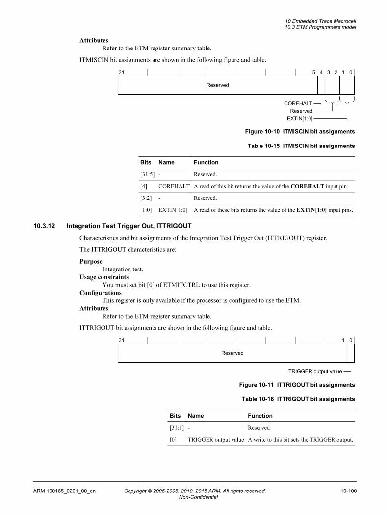
AttributesRefer to the ETM register summary table.
ITMISCIN bit assignments are shown in the following figure and table.
Reserved
31 5 4 3 2 1 0
COREHALTReserved
EXTIN[1:0]
Figure 10-10 ITMISCIN bit assignments
Table 10-15 ITMISCIN bit assignments
Bits Name Function
[31:5] - Reserved.
[4] COREHALT A read of this bit returns the value of the COREHALT input pin.
[3:2] - Reserved.
[1:0] EXTIN[1:0] A read of these bits returns the value of the EXTIN[1:0] input pins.
10.3.12 Integration Test Trigger Out, ITTRIGOUT
Characteristics and bit assignments of the Integration Test Trigger Out (ITTRIGOUT) register.
The ITTRIGOUT characteristics are:
PurposeIntegration test.
Usage constraintsYou must set bit [0] of ETMITCTRL to use this register.
ConfigurationsThis register is only available if the processor is configured to use the ETM.
AttributesRefer to the ETM register summary table.
ITTRIGOUT bit assignments are shown in the following figure and table.
Reserved
31 1 0
TRIGGER output value
Figure 10-11 ITTRIGOUT bit assignments
Table 10-16 ITTRIGOUT bit assignments
Bits Name Function
[31:1] - Reserved
[0] TRIGGER output value A write to this bit sets the TRIGGER output.
10 Embedded Trace Macrocell10.3 ETM Programmers model
ARM 100165_0201_00_en Copyright © 2005-2008, 2010, 2015 ARM. All rights reserved. 10-100Non-Confidential

10.3.13 ETM Integration Test ATB Control 2, ETM_ITATBCTR2
Characteristics and bit assignments of the ETM Integration Test ATB Control 2 (ETM_ITATBCTR2)register.
The ETM_ITATBCTR2 characteristics are:
PurposeIntegration test.
Usage constraintsYou must set bit [0] of ETMITCTRL to use this register.
ConfigurationsThis register is only available if the processor is configured to use the ETM.
AttributesRefer to the ETM register summary table.
ETM_ITATBCTR2 bit assignments are shown in the following figure and table.
Reserved
31 1 0
ATREADY input value
Figure 10-12 ETM_ITATBCTR2 bit assignments
Table 10-17 ETM_ITATBCTR2 bit assignments
Bits Name Function
[31:1] - Reserved
[0] ATREADY input value A read of this bit returns the value of the ETM ATREADY input.
10.3.14 ETM Integration Test ATB Control 0, ETM_ITATBCTR0
Characteristics and bit assignments of the Integration Test ATB Control (ETM_ITATBCTR0) register.
The ETM_ITATBCTR0 characteristics are:
PurposeIntegration test.
Usage constraintsYou must set bit [0] of ETMITCTRL to use this register.
ConfigurationsThis register is only available if the processor is configured to use the ETM.
AttributesRefer to the ETM register summary table.
ETM_ITATBCTR0 bit assignments are shown in the following figure and table.
Reserved
31 1 0
ATVALID output value
Figure 10-13 ETM_ITATBCTR0 bit assignments
10 Embedded Trace Macrocell10.3 ETM Programmers model
ARM 100165_0201_00_en Copyright © 2005-2008, 2010, 2015 ARM. All rights reserved. 10-101Non-Confidential

Table 10-18 ETM_ITATBCTR0 bit assignments
Bits Name Function
[31:1] - Reserved
[0] ATVALID output value A write to this bit sets the value of the ETM ATVALID output.
10 Embedded Trace Macrocell10.3 ETM Programmers model
ARM 100165_0201_00_en Copyright © 2005-2008, 2010, 2015 ARM. All rights reserved. 10-102Non-Confidential

Chapter 11Trace Port Interface Unit
This chapter describes the Trace Port Interface Unit (TPIU) specific to this processor.
It contains the following sections:• 11.1 About the TPIU on page 11-104.• 11.2 TPIU functional description on page 11-105.• 11.3 TPIU programmers model on page 11-107.
ARM 100165_0201_00_en Copyright © 2005-2008, 2010, 2015 ARM. All rights reserved. 11-103Non-Confidential
11.1 About the TPIUThe Cortex-M3 TPIU is an optional component that acts as a bridge between the on-chip trace data fromthe Embedded Trace Macrocell (ETM) and the Instrumentation Trace Macrocell (ITM), with separateIDs, to a data stream. The TPIU encapsulates IDs where required, and the data stream is then captured bya Trace Port Analyzer (TPA).
The Cortex-M3 TPIU is specially designed for low-cost debug. It is a special version of the CoreSightTPIU. Your implementation can replace the Cortex-M3 TPIU with other CoreSight components if yourimplementation requires the additional features of the CoreSight TPIU.
In this chapter, the term TPIU refers to the Cortex-M3 TPIU. For information about the CoreSight TPIU,see the ARM® CoreSight™ Components Technical Reference Manual.
11 Trace Port Interface Unit11.1 About the TPIU
ARM 100165_0201_00_en Copyright © 2005-2008, 2010, 2015 ARM. All rights reserved. 11-104Non-Confidential

11.2 TPIU functional descriptionFunctional description of the TPIU, including information on supported configurations and TPIU blockdiagrams.
This section contains the following subsections:• 11.2.1 TPIU block diagram on page 11-105.• 11.2.2 TPIU formatter on page 11-105.• 11.2.3 Serial Wire Output format on page 11-105.
11.2.1 TPIU block diagram
Block diagram showing the component layout of the TPIU.
ATB Interface
Formatter
APBInterface
Trace Out(serializer)
ITM ATB Slave Port
APB Slave Port
TRACECLKIN
TRACECLK
TRACEDATA [3:0]
TRACESWO
CLK Domain TRACECLKIN Domain
† ATB Interface
† ETM ATB Slave Port
† Optional component
Figure 11-1 TPIU block diagram
11.2.2 TPIU formatter
The TPIU formatter inserts source ID signals into the data packet stream so that trace data can be re-associated with its trace source. The formatter is always active when the Trace Port Mode is active.
The formatting protocol is described in the CoreSight™ Architecture Specification. You must enablesynchronization packets in the DWT to provide synchronization for the formatter.
When the formatter is enabled, half-sync packets can be inserted if there is no data to output after a framehas been started. Synchronization, caused by the distributed synchronization from the DWT, ensures thatany partial frame is completed, and at least one full synchronization packet is generated.
11.2.3 Serial Wire Output format
The TPIU can output trace data in TPIU_DEVID or TPIU_SPPR Serial Wire Output formats and can beconfigured to bypass the formatter for trace output if either SWO format is selected.
The TPIU can output trace data in a Serial Wire Output (SWO) format:• TPIU_DEVID specifies the formats that are supported.• TPIU_SPPR specifies the SWO format in use. See the ARM®v7-M Architecture Reference Manual.
11 Trace Port Interface Unit11.2 TPIU functional description
ARM 100165_0201_00_en Copyright © 2005-2008, 2010, 2015 ARM. All rights reserved. 11-105Non-Confidential

When one of the two SWO modes is selected, you can enable the TPIU to bypass the formatter for traceoutput. If the formatter is bypassed, only the ITM and DWT trace source passes through. The TPIUaccepts and discards data from the ETM. This function can be used to connect a device containing anETM to a trace capture device that is only able to capture SWO data.
11 Trace Port Interface Unit11.2 TPIU functional description
ARM 100165_0201_00_en Copyright © 2005-2008, 2010, 2015 ARM. All rights reserved. 11-106Non-Confidential

11.3 TPIU programmers modelThe TPIU registers table provides a summary of the TPIU registers. Depending on the implementation ofyour processor, the TPIU registers might not be present, or the CoreSight TPIU might be present instead.Any register that is configured as not present reads as zero.
Table 11-1 TPIU registers
Address Name Type Reset Description
0xE0040000 TPIU_SSPSR RO 0x Supported Parallel Port Size Register
0xE0040004 TPIU_CSPSR RW 0x01 Current Parallel Port Size Register
0xE0040010 TPIU_ACPR RW 0x0000 Asynchronous Clock Prescaler Register, TPIU_ACPR
0xE00400F0 TPIU_SPPR RW 0x01 Selected Pin Protocol Register
0xE0040300 TPIU_FFSR RO 0x08 Formatter and Flush Status Register, TPIU_FFSR
0xE0040304 TPIU_FFCR RW 0x102 Formatter and Flush Control Register, TPIU_FFCR
0xE0040308 TPIU_FSCR RO 0x00 Formatter Synchronization Counter Register
0xE0040EE8 TRIGGER RO 0x0 TRIGGER
0xE0040EEC FIFO data 0 RO 0x--000000 Integration ETM Data
0xE0040EF0 ITATBCTR2 RO 0x0 ITATBCTR2
0xE0040EFC FIFO data 1 RO 0x--000000 Integration ITM Data
0xE0040EF8 ITATBCTR0 RO 0x0 ITATBCTR0
0xE0040F00 ITCTRL RW 0x0 Integration Mode Control, TPIU_ITCTRL
0xE0040FA0 CLAIMSET RW 0xF Claim tag set
0xE0040FA4 CLAIMCLR RW 0x0 Claim tag clear
0xE0040FC8 DEVID RO 0xCA0/0xCA1 TPIU_DEVID
0xE0040FCC DEVTYPE RO 0x11 TPIU_DEVTYPE
0xE0040FD0 PID4 RO 0x04 Peripheral identification registers
0xE0040FD4 PID5 RO 0x00
0xE0040FD8 PID6 RO 0x00
0xE0040FDC PID7 RO 0x00
0xE0040FE0 PID0 RO 0x23
0xE0040FE4 PID1 RO 0xB9
0xE0040FE8 PID2 RO 0x3B
0xE0040FEC PID3 RO 0x00
0xE0040FF0 CID0 RO 0x0D Component identification registers
0xE0040FF4 CID1 RO 0x90
0xE0040FF8 CID2 RO 0x05
0xE0040FFC CID3 RO 0xB1
The following sections describe the TPIU registers whose implementation is specific to this processor.The Formatter, Integration Mode Control, and Claim Tag registers are described in the CoreSight™
11 Trace Port Interface Unit11.3 TPIU programmers model
ARM 100165_0201_00_en Copyright © 2005-2008, 2010, 2015 ARM. All rights reserved. 11-107Non-Confidential
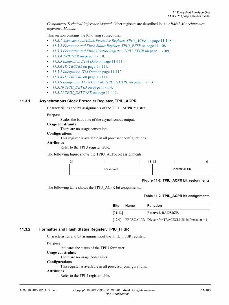
Components Technical Reference Manual. Other registers are described in the ARMv7-M ArchitectureReference Manual.
This section contains the following subsections:• 11.3.1 Asynchronous Clock Prescaler Register, TPIU_ACPR on page 11-108.• 11.3.2 Formatter and Flush Status Register, TPIU_FFSR on page 11-108.• 11.3.3 Formatter and Flush Control Register, TPIU_FFCR on page 11-109.• 11.3.4 TRIGGER on page 11-110.• 11.3.5 Integration ETM Data on page 11-111.• 11.3.6 ITATBCTR2 on page 11-111.• 11.3.7 Integration ITM Data on page 11-112.• 11.3.8 ITATBCTR0 on page 11-113.• 11.3.9 Integration Mode Control, TPIU_ITCTRL on page 11-113.• 11.3.10 TPIU_DEVID on page 11-114.• 11.3.11 TPIU_DEVTYPE on page 11-115.
11.3.1 Asynchronous Clock Prescaler Register, TPIU_ACPR
Characteristics and bit assignments of the TPIU_ACPR register.
PurposeScales the baud rate of the asynchronous output.
Usage constraintsThere are no usage constraints.
ConfigurationsThis register is available in all processor configurations.
AttributesRefer to the TPIU register table.
The following figure shows the TPIU_ACPR bit assignments.
31 13 0
Reserved
12
PRESCALER
Figure 11-2 TPIU_ACPR bit assignments
The following table shows the TPIU_ACPR bit assignments.
Table 11-2 TPIU_ACPR bit assignments
Bits Name Function
[31:13] - Reserved. RAZ/SBZP.
[12:0] PRESCALER Divisor for TRACECLKIN is Prescaler + 1.
11.3.2 Formatter and Flush Status Register, TPIU_FFSR
Characteristics and bit assignments.of the TPIU_FFSR register.
PurposeIndicates the status of the TPIU formatter.
Usage constraintsThere are no usage constraints.
ConfigurationsThis register is available in all processor configurations.
AttributesRefer to the TPIU register table.
11 Trace Port Interface Unit11.3 TPIU programmers model
ARM 100165_0201_00_en Copyright © 2005-2008, 2010, 2015 ARM. All rights reserved. 11-108Non-Confidential

The following figure shows the TPIU_FFSR bit assignments.
31 2 0
Reserved
1
FlInProg
3
FtStoppedTCPresentFtNonStop
4
Figure 11-3 TPIU_FFSR bit assignments
The following table shows the TPIU_FFSR bit assignments.
Table 11-3 TPIU_FFSR bit assignments
Bits Name Function
[31:4] - Reserved
[3] FtNonStop Formatter cannot be stopped
[2] TCPresent This bit always reads zero
[1] FtStopped This bit always reads zero
[0] FlInProg This bit always reads zero
11.3.3 Formatter and Flush Control Register, TPIU_FFCR
Characteristics and bit assignments of the TPIU_FFCR register.
PurposeControls the TPIU formatter.
Usage constraintsThere are no usage constraints.
ConfigurationsThis register is available in all processor configurations.
AttributesRefer to the TPIU register table.
The following figure shows the TPIU_FFCR bit assignments.
Reserved
31 9 8 7 2 1 0
Reserved
TrigIn EnFContReserved
Figure 11-4 TPIU_FFCR bit assignments
The following table shows the TPIU_FFCR bit assignments.
Table 11-4 TPIU_FFCR bit assignments
Bits Name Function
[31:9] - Reserved.
[8] TrigIn This bit Reads-As-One (RAO), specifying that triggers are inserted when a trigger pin is asserted.
[7:2] - Reserved.
11 Trace Port Interface Unit11.3 TPIU programmers model
ARM 100165_0201_00_en Copyright © 2005-2008, 2010, 2015 ARM. All rights reserved. 11-109Non-Confidential
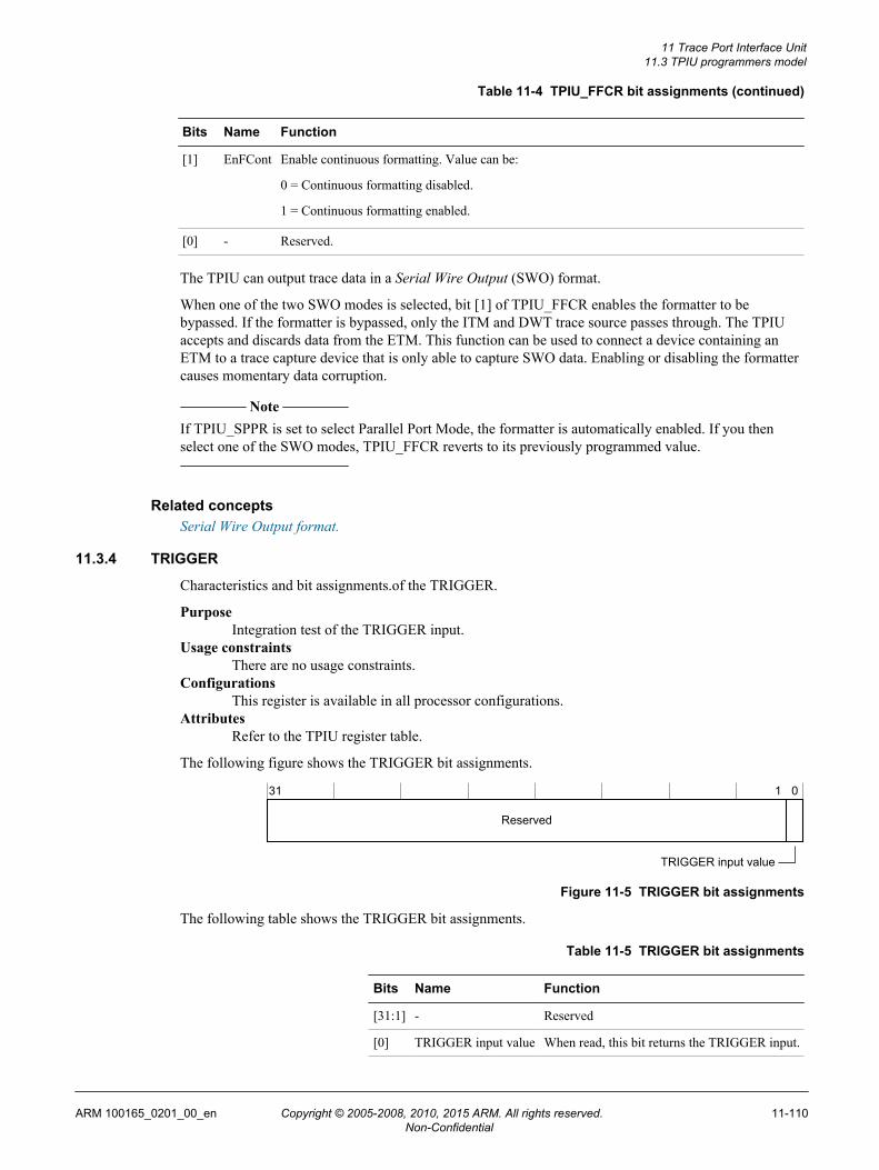
Table 11-4 TPIU_FFCR bit assignments (continued)
Bits Name Function
[1] EnFCont Enable continuous formatting. Value can be:
0 = Continuous formatting disabled.
1 = Continuous formatting enabled.
[0] - Reserved.
The TPIU can output trace data in a Serial Wire Output (SWO) format.
When one of the two SWO modes is selected, bit [1] of TPIU_FFCR enables the formatter to bebypassed. If the formatter is bypassed, only the ITM and DWT trace source passes through. The TPIUaccepts and discards data from the ETM. This function can be used to connect a device containing anETM to a trace capture device that is only able to capture SWO data. Enabling or disabling the formattercauses momentary data corruption.
Note
If TPIU_SPPR is set to select Parallel Port Mode, the formatter is automatically enabled. If you thenselect one of the SWO modes, TPIU_FFCR reverts to its previously programmed value.
Related conceptsSerial Wire Output format.
11.3.4 TRIGGER
Characteristics and bit assignments.of the TRIGGER.
PurposeIntegration test of the TRIGGER input.
Usage constraintsThere are no usage constraints.
ConfigurationsThis register is available in all processor configurations.
AttributesRefer to the TPIU register table.
The following figure shows the TRIGGER bit assignments.
Reserved
31 1 0
TRIGGER input value
Figure 11-5 TRIGGER bit assignments
The following table shows the TRIGGER bit assignments.
Table 11-5 TRIGGER bit assignments
Bits Name Function
[31:1] - Reserved
[0] TRIGGER input value When read, this bit returns the TRIGGER input.
11 Trace Port Interface Unit11.3 TPIU programmers model
ARM 100165_0201_00_en Copyright © 2005-2008, 2010, 2015 ARM. All rights reserved. 11-110Non-Confidential

11.3.5 Integration ETM Data
Characteristics and bit assignments of the Integration ETM Data register.
PurposeTrace data integration testing.
Usage constraintsYou must set bit [1] of TPIU_ITCTRL to use this register.
ConfigurationsThis register is available in all processor configurations.
AttributesRefer to the TPIU register table.
The following figure shows the Integration ETM Data bit assignments.
ETM data 2 ETM data 1 ETM data 0
31 029 2728 26 2425 23 16 15 8 7
ETM byte countETM ATVALIDITM byte countITM ATVALID
30
Reserved
Figure 11-6 Integration ETM Data bit assignments
The following table shows the Integration ETM Data bit assignments.
Table 11-6 Integration ETM Data bit assignments
Bits Name Function
[31:30] - Reserved
[29] ITM ATVALID input Returns the value of the ITM ATVALID signal.
[28:27] ITM byte count Number of bytes of ITM trace data since last read of Integration ITM Data Register.
[26] ETM ATVALID input Returns the value of the ETM ATVALID signal.
[25:24] ETM byte count Number of bytes of ETM trace data since last read of Integration ETM Data Register.
[23:16] ETM data 2 ETM trace data. The TPIU discards this data when the register is read.
[15:8] ETM data 1
[7:0] ETM data 0
11.3.6 ITATBCTR2
Characteristics and bit assignments of the ITATBCTR2 register.
PurposeIntegration test.
Usage constraintsYou must set bit [0] of TPIU_ITCTRL to use this register.
ConfigurationsThis register is available in all processor configurations.
AttributesRefer to the TPIU register table.
The following figure shows the ITATBCTR2 bit assignments.
11 Trace Port Interface Unit11.3 TPIU programmers model
ARM 100165_0201_00_en Copyright © 2005-2008, 2010, 2015 ARM. All rights reserved. 11-111Non-Confidential

31 0
Reserved
1
ATREADY1ATREADY2
Figure 11-7 ITATBCTR2 bit assignments
The following table shows the ITATBCTR2 bit assignments.
Table 11-7 ITATBCTR2 bit assignments
Bits Name Function
[31:1] - Reserved
[0] ATREADY1, ATREADY2 This bit sets the value of both the ETM and ITM ATREADY outputs, if the TPIU is in integrationtest mode.
11.3.7 Integration ITM Data
Characteristics and bit assignments of the Integration ITM Data register.
PurposeTrace data integration testing.
Usage constraintsYou must set bit [1] of TPIU_ITCTRL to use this register.
ConfigurationsThis register is available in all processor configurations.
AttributesRefer to the TPIU register table.
The following figure shows the Integration ITM Data bit assignments.
31 30 29 28 27 26 25 24 23 16 15 8 7 0
ITM data 2 ITM data 1 ITM data 0
ETM byte countETM ATVALID inputITM byte countITM ATVALID inputReserved
Figure 11-8 Integration ITM Data bit assignments
The following table shows the Integration ITM Data bit assignments.
Table 11-8 Integration ITM Data bit assignments
Bits Name Function
[31:30] - Reserved
[29] ITM ATVALID input Returns the value of the ITM ATVALID signal.
[28:27] ITM byte count Number of bytes of ITM trace data since last read of Integration ITM Data Register.
[26] ETM ATVALID input Returns the value of the ETM ATVALID signal.
[25:24] ETM byte count Number of bytes of ETM trace data since last read of Integration ETM Data Register.
11 Trace Port Interface Unit11.3 TPIU programmers model
ARM 100165_0201_00_en Copyright © 2005-2008, 2010, 2015 ARM. All rights reserved. 11-112Non-Confidential

Table 11-8 Integration ITM Data bit assignments (continued)
Bits Name Function
[23:16] ITM data 2 ITM trace data. The TPIU discards this data when the register is read.
[15:8] ITM data 1
[7:0] ITM data 0
11.3.8 ITATBCTR0
Characteristics and bit assignments of the ITATBCTR0 register.
PurposeIntegration test.
Usage constraintsThere are no usage constraints.
ConfigurationsThis register is available in all processor configurations.
AttributesRefer to the TPIU register table.
The following figure shows the ITATBCTR0 bit assignments.
31 0
Reserved
1
ATVALID1ATVALID2
Figure 11-9 ITATBCTR0 bit assignments
The following table shows the ITATBCTR0 bit assignments.
Table 11-9 ITATBCTR0 bit assignments
Bits Name Function
[31:1] - Reserved
[0] ATVALID1, ATVALID2 A read of this bit returns the value of ATVALIDS1 OR-ed with ATVALIDS2.
11.3.9 Integration Mode Control, TPIU_ITCTRL
Characteristics and bit assignments of the TPIU_ITCTRL register.
PurposeSpecifies normal or integration mode for the TPIU.
Usage constraintsThere are no usage constraints.
ConfigurationsThis register is available in all processor configurations.
AttributesRefer to the TPIU register table.
The following figure shows the TPIU_ITCTRL bit assignments.
11 Trace Port Interface Unit11.3 TPIU programmers model
ARM 100165_0201_00_en Copyright © 2005-2008, 2010, 2015 ARM. All rights reserved. 11-113Non-Confidential
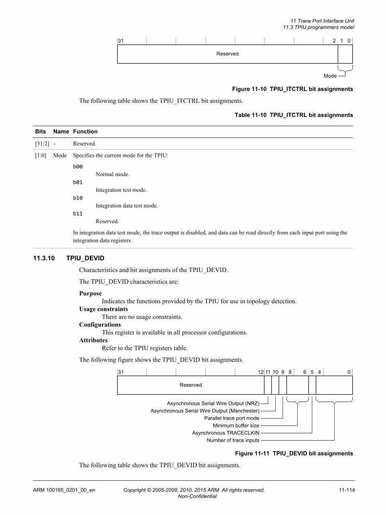
Reserved
31 2 1 0
Mode
Figure 11-10 TPIU_ITCTRL bit assignments
The following table shows the TPIU_ITCTRL bit assignments.
Table 11-10 TPIU_ITCTRL bit assignments
Bits Name Function
[31:2] - Reserved.
[1:0] Mode Specifies the current mode for the TPIU:
b00Normal mode.
b01Integration test mode.
b10Integration data test mode.
b11Reserved.
In integration data test mode, the trace output is disabled, and data can be read directly from each input port using theintegration data registers.
11.3.10 TPIU_DEVID
Characteristics and bit assignments of the TPIU_DEVID.
The TPIU_DEVID characteristics are:
PurposeIndicates the functions provided by the TPIU for use in topology detection.
Usage constraintsThere are no usage constraints.
ConfigurationsThis register is available in all processor configurations.
AttributesRefer to the TPIU registers table.
The following figure shows the TPIU_DEVID bit assignments.
Reserved
31 12 11 10 9 8 6 5 0
Asynchronous Serial Wire Output (NRZ)Asynchronous Serial Wire Output (Manchester)
Parallel trace port modeMinimum buffer size
Asynchronous TRACECLKIN
4
Number of trace inputs
Figure 11-11 TPIU_DEVID bit assignments
The following table shows the TPIU_DEVID bit assignments.
11 Trace Port Interface Unit11.3 TPIU programmers model
ARM 100165_0201_00_en Copyright © 2005-2008, 2010, 2015 ARM. All rights reserved. 11-114Non-Confidential

Table 11-11 TPIU_DEVID bit assignments
Bits Name Function
[31:12] - Reserved
[11] Asynchronous Serial Wire Output(NRZ)
This bit Reads-As-One (RAO), indicating that the output is supported.
[10] Asynchronous Serial Wire Output(Manchester)
This bit Reads-As-One (RAO), indicating that the output is supported.
[9] Parallel trace port mode This bit Reads-As-Zero (RAZ), indicating that parallel trace port mode is supported.
[8:6] Minimum buffer size Specifies the minimum TPIU buffer size:
0b010 = 4 bytes.
[5] Asynchronous TRACECLKIN Specifies whether TRACECLKIN can be asynchronous to CLK:
0b1 = TRACECLKIN can be asynchronous to CLK.
[4:0] Number of trace inputs Specifies the number of trace inputs:
0b00000 = 1 input
0b00001 = 2 inputs
If your implementation includes an ETM, the value of this field is 0b00001.
11.3.11 TPIU_DEVTYPE
The Device Type Identifier Register is read-only. It provides a debugger with information about thecomponent when the Part Number field is not recognized. The debugger can then report this information.
The TPIU_DEVTYPE characteristics are:
PurposeIndicates the type of functionality the component supports.
Usage ConstraintsThere are no usage constraints.
ConfigurationsThis register is available in all processor configurations.
AttributesThe Device Type reads as 0x11 and indicates this device is a trace sink and specifically a TPIU.
Reserved
31 78 0
Sub type
4
Major type
3
Figure 11-12 TPIU_DEVTYPE bit assignments
11 Trace Port Interface Unit11.3 TPIU programmers model
ARM 100165_0201_00_en Copyright © 2005-2008, 2010, 2015 ARM. All rights reserved. 11-115Non-Confidential

Appendix ARevisions
The technical changes between released issues of this book.
It contains the following sections:• A.1 Revisions on page Appx-A-117.
ARM 100165_0201_00_en Copyright © 2005-2008, 2010, 2015 ARM. All rights reserved. Appx-A-116Non-Confidential

A.1 RevisionsThis appendix describes the technical changes between released issues of this book.
Table A-1 Differences between issue E and issue F
Change Location
Introductory processor information updated Issue H distributes this information between 1.1 About theprocessor on page 1-12 and 1.2 Processor features liston page 1-13 and removes duplicate information from thesesections.
Processor block diagram updated 2.1 About the functions on page 2-22
Introductory information added, including:• TPIU subsection.• Addition of note to SW/SWJ-DP subsection.• ROM table subsection.
Issue H removes this information.
Introductory processor core information updated
APB bus now version 3.0 1.5.3 Architecture and protocol information on page 1-18
Configurable options information expanded to include:• Added DWT configurability information.• New subsections for ITM, AHB-AP, FPB and Observation.
1.4 Optional implementation components on page 1-15
New subsection added to list changes in functionality between r1p1and r2p0
1.6.3 List of differences in functionality between r1p1 andr2p0 on page 1-19
Information about the programmers model updated Issue H distributes this information between 1.1 About theprocessor on page 1-12 and 3.2 Modes of operation andexecution on page 3-30.
Definition of ICI field of Execution Program Status Register updated Issue H removes this information.
Table of nonsupported Thumb instructions removed.
Second footnote on Table 5-1 removed. Issue H removes this information.
Addition of note to vector table and reset description
Description of SLEEPING and SLEEPDEEP signals updated.
Description of extending sleep functionality added
Addition of Auxiliary Control Register Auxiliary Control Register, ACTLR
Irq 0 to 31 Priority Register amended to Irq 0 to 3 Priority Register Issue H removes this information.
Irq 236 to 239 Priority Register amended to Irq 224 to 239 PriorityRegister
HCLK changed to FCLK
Addition of ascending MPU region priority information 5.1 About the MPU on page 5-55
Extra paragraph added. Issue H removes this information.
Debug Core Register Selector Register REGSEL bit field functionupdated
Paragraph added about removing FPB
A RevisionsA.1 Revisions
ARM 100165_0201_00_en Copyright © 2005-2008, 2010, 2015 ARM. All rights reserved. Appx-A-117Non-Confidential
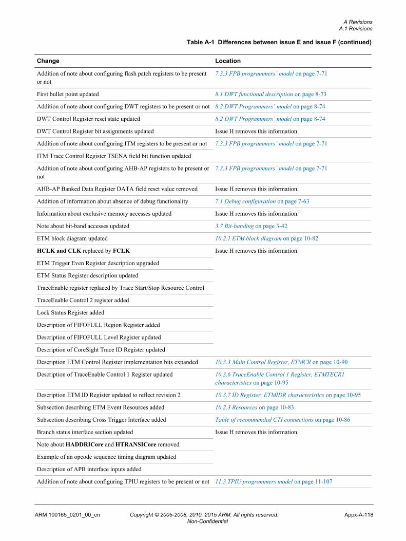
Table A-1 Differences between issue E and issue F (continued)
Change Location
Addition of note about configuring flash patch registers to be presentor not
7.3.3 FPB programmers’ model on page 7-71
First bullet point updated 8.1 DWT functional description on page 8-73
Addition of note about configuring DWT registers to be present or not 8.2 DWT Programmers’ model on page 8-74
DWT Control Register reset state updated 8.2 DWT Programmers’ model on page 8-74
DWT Control Register bit assignments updated Issue H removes this information.
Addition of note about configuring ITM registers to be present or not 7.3.3 FPB programmers’ model on page 7-71
ITM Trace Control Register TSENA field bit function updated
Addition of note about configuring AHB-AP registers to be present ornot
7.3.3 FPB programmers’ model on page 7-71
AHB-AP Banked Data Register DATA field reset value removed Issue H removes this information.
Addition of information about absence of debug functionality 7.1 Debug configuration on page 7-63
Information about exclusive memory accesses updated Issue H removes this information.
Note about bit-band accesses updated 3.7 Bit-banding on page 3-42
ETM block diagram updated 10.2.1 ETM block diagram on page 10-82
HCLK and CLK replaced by FCLK Issue H removes this information.
ETM Trigger Even Register description upgraded
ETM Status Register description updated
TraceEnable register replaced by Trace Start/Stop Resource Control
TraceEnable Control 2 register added
Lock Status Register added
Description of FIFOFULL Region Register added
Description of FIFOFULL Level Register updated
Description of CoreSight Trace ID Register updated
Description ETM Control Register implementation bits expanded 10.3.3 Main Control Register, ETMCR on page 10-90
Description of TraceEnable Control 1 Register updated 10.3.6 TraceEnable Control 1 Register, ETMTECR1characteristics on page 10-95
Description ETM ID Register updated to reflect revision 2 10.3.7 ID Register, ETMIDR characteristics on page 10-95
Subsection describing ETM Event Resources added 10.2.3 Resources on page 10-83
Subsection describing Cross Trigger Interface added Table of recommended CTI connections on page 10-86
Branch status interface section updated Issue H removes this information.
Note about HADDRICore and HTRANSICore removed
Example of an opcode sequence timing diagram updated
Description of APB interface inputs added
Addition of note about configuring TPIU registers to be present or not 11.3 TPIU programmers model on page 11-107
A RevisionsA.1 Revisions
ARM 100165_0201_00_en Copyright © 2005-2008, 2010, 2015 ARM. All rights reserved. Appx-A-118Non-Confidential
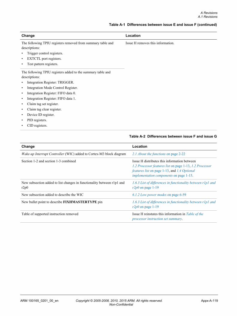
Table A-1 Differences between issue E and issue F (continued)
Change Location
The following TPIU registers removed from summary table anddescriptions:• Trigger control registers.• EXTCTL port registers.• Test pattern registers.
Issue H removes this information.
The following TPIU registers added to the summary table anddescriptions:• Integration Register: TRIGGER.• Integration Mode Control Register.• Integration Register: FIFO data 0.• Integration Register: FIFO data 1.• Claim tag set register.• Claim tag clear register.• Device ID register.• PID registers.• CID registers.
Table A-2 Differences between issue F and issue G
Change Location
Wake-up Interrupt Controller (WIC) added to Cortex-M3 block diagram 2.1 About the functions on page 2-22
Section 1-2 and section 1-3 combined Issue H distributes this information between1.2 Processor features list on page 1-13, 1.2 Processorfeatures list on page 1-13, and 1.4 Optionalimplementation components on page 1-15.
New subsection added to list changes in functionality between r1p1 andr2p0
1.6.3 List of differences in functionality between r1p1 andr2p0 on page 1-19
New subsection added to describe the WIC 6.1.2 Low power modes on page 6-59
New bullet point to describe FIXHMASTERTYPE pin 1.6.3 List of differences in functionality between r1p1 andr2p0 on page 1-19
Table of supported instruction removed Issue H reinstates this information in Table of theprocessor instruction set summary.
A RevisionsA.1 Revisions
ARM 100165_0201_00_en Copyright © 2005-2008, 2010, 2015 ARM. All rights reserved. Appx-A-119Non-Confidential

Table A-2 Differences between issue F and issue G (continued)
Change Location
More information added about the stacked xPSR Issue H removes this information.
Reset value of Configuration Control Register changed to 0x00000200
System and Vendor_SYS memory regions added to table of memoryregion permissions
Memory region for Private Peripheral Bus changed to +0000000
SLEEPHOLDREQ changed to SLEEPHOLDREQn
SLEEPHOLDACK changed to SLEEPHOLDACKn
DEEPSLEEP signal changed to SLEEPDEEP
DBGRESTARTACK changed to DBGRESTARTED
DBGRESTARTREQ changed to DBGRESTART
New subsection added to describe the WIC
Address of Irq 224 to 239 Priority Register changed to 0xE000E4EC
Enhanced description of function of C_MASKINTS field
Settings for DWT Function Registers updated
Minor change to timing information of ETMIA
Change to timing information for ETMIVALID Issue H removes this information.
SLEEPHOLDREQn removed from table of miscellaneous input portstiming parameters
Table of low power input ports timing parameters added
FIXHMASTERTYPE added to table of debug input ports timingparameters
Input changed to Output in table header
SLEEPING, SLEEPDEEP, and SLEEPHOLDACKn removed from tableof miscellaneous output ports timing parameters
SLEEPDEEP, SLEEPING, SLEEPHOLDREQ, andSLEEPHOLDACK removed
New section added to describe the low power interface signals
New section added to describe the WIC interface signals
SLEEPHOLDACKn removed from table of miscellaneous signals
Asserted changed to de-asserted in the description of SLEEPHOLDREQnin table of low power interface signals
FIXMASTERTPYE added to list of AHB-AP interface signals
Note
Issue H of this book is significantly reorganized and simplified to eliminate duplication of informationcontained in the ARM Architecture Reference Manual and other ARM documentation.
A RevisionsA.1 Revisions
ARM 100165_0201_00_en Copyright © 2005-2008, 2010, 2015 ARM. All rights reserved. Appx-A-120Non-Confidential
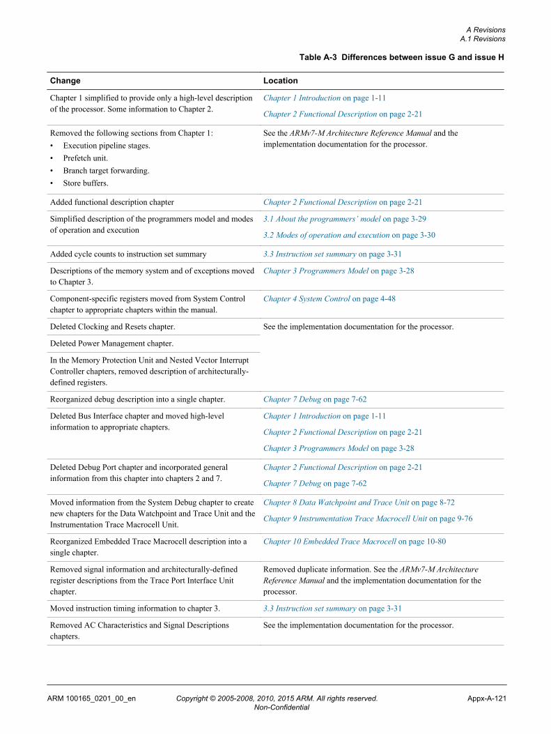
Table A-3 Differences between issue G and issue H
Change Location
Chapter 1 simplified to provide only a high-level descriptionof the processor. Some information to Chapter 2.
Chapter 1 Introduction on page 1-11
Chapter 2 Functional Description on page 2-21
Removed the following sections from Chapter 1:• Execution pipeline stages.• Prefetch unit.• Branch target forwarding.• Store buffers.
See the ARMv7-M Architecture Reference Manual and theimplementation documentation for the processor.
Added functional description chapter Chapter 2 Functional Description on page 2-21
Simplified description of the programmers model and modesof operation and execution
3.1 About the programmers’ model on page 3-29
3.2 Modes of operation and execution on page 3-30
Added cycle counts to instruction set summary 3.3 Instruction set summary on page 3-31
Descriptions of the memory system and of exceptions movedto Chapter 3.
Chapter 3 Programmers Model on page 3-28
Component-specific registers moved from System Controlchapter to appropriate chapters within the manual.
Chapter 4 System Control on page 4-48
Deleted Clocking and Resets chapter. See the implementation documentation for the processor.
Deleted Power Management chapter.
In the Memory Protection Unit and Nested Vector InterruptController chapters, removed description of architecturally-defined registers.
Reorganized debug description into a single chapter. Chapter 7 Debug on page 7-62
Deleted Bus Interface chapter and moved high-levelinformation to appropriate chapters.
Chapter 1 Introduction on page 1-11
Chapter 2 Functional Description on page 2-21
Chapter 3 Programmers Model on page 3-28
Deleted Debug Port chapter and incorporated generalinformation from this chapter into chapters 2 and 7.
Chapter 2 Functional Description on page 2-21
Chapter 7 Debug on page 7-62
Moved information from the System Debug chapter to createnew chapters for the Data Watchpoint and Trace Unit and theInstrumentation Trace Macrocell Unit.
Chapter 8 Data Watchpoint and Trace Unit on page 8-72
Chapter 9 Instrumentation Trace Macrocell Unit on page 9-76
Reorganized Embedded Trace Macrocell description into asingle chapter.
Chapter 10 Embedded Trace Macrocell on page 10-80
Removed signal information and architecturally-definedregister descriptions from the Trace Port Interface Unitchapter.
Removed duplicate information. See the ARMv7-M ArchitectureReference Manual and the implementation documentation for theprocessor.
Moved instruction timing information to chapter 3. 3.3 Instruction set summary on page 3-31
Removed AC Characteristics and Signal Descriptionschapters.
See the implementation documentation for the processor.
A RevisionsA.1 Revisions
ARM 100165_0201_00_en Copyright © 2005-2008, 2010, 2015 ARM. All rights reserved. Appx-A-121Non-Confidential

Table A-4 Differences between issue H and issue I
Change Location
Updated Bus interfaces information. 2.3.1 Bus interfaces on page 2-25
Added information on Private Peripheral Bus Private Peripheral Bus (PPB) on page 2-26
Updated Load/store timings information. 3.3.2 Load/store timings on page 3-35
Updated Exclusive monitor information. 3.6 Exclusive monitor on page 3-41
Updated Reset values for Register summary information. 4.1 System control registers on page 4-49
Reset values updated. 4.1 System control registers on page 4-49
Updated Reset values for MPU register information. 5.3 MPU programmers model table on page 5-57
Changed address range of NVIC_IPR registers. 6.2.1 Table of NVIC registers on page 6-60
Updated values for the Cortex-M3 ROM tableinformation and added Peripheral IDs 5-7.
ROM table identification and entries
Added Timestamp format information. 10.2.4 Timestamp format on page 10-85
Added ETM register descriptions. 10.3.2 ETM register summary table on page 10-88
Added ETMCNTRLDVR1 ETM register. 10.3.2 ETM register summary table on page 10-88
Changed reset values for ETMVCCR and ETMCCER. 10.3.2 ETM register summary table on page 10-88
Updated ETMCR register bit assignments. 10.3.3 Main Control Register, ETMCR on page 10-90
Updated ETMCCR bit assignments. 10.3.4 Configuration Code Register, ETMCCR on page 10-93
Updated ETMCCER bit assignments. 10.3.8 Configuration Code Extension Register, ETMCCER characteristicson page 10-96
Added TPIU_DEVTYPE TPIU Register. Changed resetvalues.
11.3 TPIU programmers model on page 11-107
Updated TPIU Formatter information 11.2.2 TPIU formatter on page 11-105
Replaced FIFO 0 with ETM. Integration ETM Data
Integration ITM Data
Replaced FIFO 1 with ITM Integration ETM Data
Integration ITM Data
Added TPIU_DEVTYPE Register description. 11.3 TPIU programmers model on page 11-107
A RevisionsA.1 Revisions
ARM 100165_0201_00_en Copyright © 2005-2008, 2010, 2015 ARM. All rights reserved. Appx-A-122Non-Confidential