technical reference - spectrum...
TRANSCRIPT

TMS320C5535 eZdspTM
2011 DSP Development Systems
ReferenceTechnical


TMS320C5535 eZdspTM
Technical Reference
514585-0001 Rev. A August 2011
SPECTRUM DIGITAL, INC.12502 Exchange Drive, Suite 440 Stafford, TX. 77477
Tel: 281.494.4505 Fax: [email protected] www.spectrumdigital.com

IMPORTANT NOTICE
Spectrum Digital, Inc. reserves the right to make changes to its products or to discontinue anyproduct or service without notice. Customers are advised to obtain the latest version of relevantinformation to verify that the data being relied on is current before placing orders.
Spectrum Digital, Inc. warrants performance of its products and related software to currentspecifications in accordance with Spectrum Digital’s standard warranty. Testing and other qualitycontrol techniques are utilized to the extent deemed necessary to support this warranty.
Please be aware that the products described herein are not intended for use in life-support appliances, devices, or systems. Spectrum Digital does not warrant nor is Spectrum Digital liable for the product described herein to be used in other than a development environment.
Spectrum Digital, Inc. assumes no liability for applications assistance, customer product design, software performance, or infringement of patents or services described herein. Nor does SpectrumDigital warrant or represent any license, either express or implied, is granted under any patent right,copyright, or other intellectual property right of Spectrum Digital, Inc. covering or relating to anycombination, machine, or process in which such Digital Signal Processing development products orservices might be or are used.
WARNING
This equipment is intended for use in a laboratory test environment only. It generates, uses, and canradiate radio frequency energy and has not been tested for compliance with the limits of computingdevices pursuant to subpart J of part 15 of FCC rules, which are designed to provide reasonableprotection against radio frequency interference. Operation of this equipment in other environmentsmay cause interference with radio communications, in which case the user at his own expense will berequired to take whatever measures necessary to correct this interference.
TRADEMARKS
Windows 2000, Windows XP, Windows Vista are registered trademarks of Microsoft Corp
Code Composer Studio IDE is a trademark of Texas Instruments
“eZdsp” is a trademark of Spectrum Digital, Inc.
Copyright © 2011 Spectrum Digital, Inc.

Contents
1 Introduction to the TMS320C5535 eZdsp . . . . . . . . . . . . . . . . . . . . . . . . . . . . . . . . . . 1-1 Provides a description of the TMS320C5535 eZdsp, and key features. 1.0 Overview of the TMS320C5535 eZdsp . . . . . . . . . . . . . . . . . . . . . . . . . . . . . . . . . . . . 1-2 1.2 Key Features of the TMS320C5535 eZdsp . . . . . . . . . . . . . . . . . . . . . . . . . . . . . . . . 1-3 1.3 C5535 eZdsp Block Diagram . . . . . . . . . . . . . . . . . . . . . . . . . . . . . . . . . . . . . . . . . . . . . 1-4 1.4 C5535 eZdsp Memory Map . . . . . . . . . . . . . . . . . . . . . . . . . . . . . . . . . . . . . . . . . . . . . 1-4 1.5 C5535 eZdsp I2C Addressing . . . . . . . . . . . . . . . . . . . . . . . . . . . . . . . . . . . . . . . . . . . . 1-52 Operation and Physical Specifications . . . . . . . . . . . . . . . . . . . . . . . . . . . . . . . . . . . . . . 2-1 Describes the operation and physical layout of the TMS320C5535 eZdsp and its connectors. 2.0 Board Layout . . . . . . . . . . . . . . . . . . . . . . . . . . . . . . . . . . . . . . . . . . . . . . . . . . . . . . . 2-2 2.1 Connector Index . . . . . . . . . . . . . . . . . . . . . . . . . . . . . . . . . . . . . . . . . . . . . . . . . . . . 2-3 2.1.1 J1, C5535 USB Connector . . . . . . . . . . . . . . . . . . . . . . . . . . . . . . . . . . . . . . . . . . 2-4 2.1.2 J2, XDS100 USB Connector . . . . . . . . . . . . . . . . . . . . . . . . . . . . . . . . . . . . . . . . 2-4 2.1.3 J3, Audio In Connector . . . . . . . . . . . . . . . . . . . . . . . . . . . . . . . . . . . . . . . . . . . . . 2-5 2.1.4 J4, Audio Out Connector . . . . . . . . . . . . . . . . . . . . . . . . . . . . . . . . . . . . . . . . . . . . 2-6 2.1.5 J5, LCD Interface . . . . . . . . . . . . . . . . . . . . . . . . . . . . . . . . . . . . . . . . . . . . . . . . . . 2-7 2.1.6 J6, Micro SD Card Connector . . . . . . . . . . . . . . . . . . . . . . . . . . . . . . . . . . . . . . . 2-7 2.1.7 P1, P3, Wireless Interface . . . . . . . . . . . . . . . . . . . . . . . . . . . . . . . . . . . . . . . . . . 2-8 2.1.6 P2, Expansion Connector . . . . . . . . . . . . . . . . . . . . . . . . . . . . . . . . . . . . . . . . . . . 2-9 2.2 System LEDs . . . . . . . . . . . . . . . . . . . . . . . . . . . . . . . . . . . . . . . . . . . . . . . . . . . . . 2-11 2.3 Switches . . . . . . . . . . . . . . . . . . . . . . . . . . . . . . . . . . . . . . . . . . . . . . . . . . . . . . . . . 2-11 2.3.1 SW1, SW2, Momentary Push Button Switches . . . . . . . . . . . . . . . . . . . . . . . . 2-11 2.3.2 SW3, 4 Position DIP Switch . . . . . . . . . . . . . . . . . . . . . . . . . . . . . . . . . . . . . . . 2-12 2.4 Jumpers . . . . . . . . . . . . . . . . . . . . . . . . . . . . . . . . . . . . . . . . . . . . . . . . . . . . . . . . . 2-13 2.5 Test Points . . . . . . . . . . . . . . . . . . . . . . . . . . . . . . . . . . . . . . . . . . . . . . . . . . . . . . . . 2-14A Schematics . . . . . . . . . . . . . . . . . . . . . . . . . . . . . . . . . . . . . . . . . . . . . . . . . . . . . . . . . . . . . . A-1 Contains the schematics for the TMS320C5535 eZdspB Mechanical Information . . . . . . . . . . . . . . . . . . . . . . . . . . . . . . . . . . . . . . . . . . . . . . . . . . B-1 Contains the mechanical information about the TMS320C5535 eZdsp

About This Manual
This document describes the board level operations of the TMS320C5535 eZdsp.The eZdsp is based on the Texas Instruments TMS320C5535 Digital Signal Processor.
The TMS320C5535 eZdsp is a USB based printed circuit board (PCB) that allowsengineers and software developers to evaluate certain characteristics of theTMS320C5535 DSP.
Notational Conventions
This document uses the following conventions.
The TMS320C5535 eZdsp will sometimes be referred to as the C5535 eZdsp, oreZdsp.
Program listings, program examples, and interactive displays are shown is a specialitalic typeface. Here is a sample program listing.
equations!rd = !strobe&rw;
Information About Cautions
This book may contain cautions.This is an example of a caution statement.A caution statement describes a situation that could potentially damage your software,or hardware, or other equipment. The information in a caution is provided for yourprotection. Please read each caution carefully.
Related Documents
Texas Instruments Code Composer Studio IDE Users GuideData sheet for the TMS320C5535

Chapter 1Introduction to the
TMS320C5535 eZdsp
This chapter provides you with a description of the C5535 eZdsp along with the keyfeatures.
Topic Page1.0 Overview of the TMS320C5535 eZdsp 1-21.1 Key Features of the TMS320C5535 eZdsp 1-31.2 C5535 eZdsp Block Diagram 1-41.3 C5535 eZdsp Memory Map 1-41.4 C5535 eZdsp I2C Addressing 1-5
1-1

Spectrum Digital, Inc
1.0 Overview of the C5535 eZdsp
The C5535 eZdsp is an evaluation tool for the Texas Instruments TMS320C5535Digital Signal Processor (DSP). This USB bus powered tool allows the user to evaluatethe following items:
• The TMS320C5535 processor along with its peripherals
• The TLV320AIC3204 codec
• The Code Composer Studio IDETM software development tools
C5535 DSP
ExpansionConnector
Figure 1-1, Key Features of the C5535 eZdsp (top)
USB connectorWireless
XF LED
LEDs
Display
Pushbuttons
Stereo In
Stereo Out
SPI Flash
AIC3204
USBEmulationConnector
Interface
ExpansionConnector
Figure 1-2, Key Features of the C5535 eZdsp (bottom)
DisplayConnector
MIcro SD Card Connector
1-2 TMS320C5535 eZdsp Technical Reference Manual

Spectrum Digital, Inc
1.1 Key Features of the C5535 eZdsp
The C5535 eZdsp has the following features:
• Texas Instrument’s TMS320C5535 Digital Signal Processor
• Texas Instruments TLV320AIC3204 Stereo Codec (stereo in, stereo out)
• Micro SD card connector
• USB 2.0 interface to C5535 processor
• 8 Mbytes SPI flash
• I2C OLED display
• 5 user controlled LEDs
• 2 user readable push button switches
• 3 INA219 I2C Current/Power Monitors
• Embedded USB XDS100 JTAG emulator
• Wireless interface
• Expansion edge connector
• Power measurement test points
• Power provided by USB interface
• Compatible with Texas Instruments Code Composer Studio v4
• USB cable
1-3

Spectrum Digital, Inc
1.2 C5535 eZdsp Block Diagram
The block diagram of the C5535 eZdsp is shown below.
1.3 C5535 eZdsp Memory Map
The C5535 eZdsp supports on chip DARAM, SARAM, and off chip SPI Flash. Theaddressing for each of these memory blocks is shown in the figure below.
Note: MPNMC bit in ST3 Status Register is cleared(0) at RESET so the C5535 will attempt to execute its boot load sequence.
Figure 1-3, C5535 eZdsp Block Diagram
I2C Bus
Stereo in
Stereo Out
96 x 16 pixelOLED Display
P1
P3LEDs
USB
USBJTAG
I2S2
P2
AnalogInput 1
SW1 SW2
EmbeddedXDS100 JTAG
SPIFlash
AIC3204
MicroSD(on back)
USB
SPIUART
GPIO
TMS320C5535
3.3VIO
LDO
INA219
(MMR Reserved)Internal DARAMInternal SARAM
RESERVED
RESERVED(if MPNMC=1)
ROM(in MPNMC=0)
MEMORY BLOCKSCPU ByteAddress000000h
0000C0h00FFFFh010000h
04FFFFh050000h7FFFFFh800000h
BFFFFFhC00000h
DFFFFFhE00000hE03FFFhF00000h
FDFFFFhFE0000h
FFFFFFhFigure 1-4, C5535 eZdsp Memory Map
1-4 TMS320C5535 eZdsp Technical Reference Manual

Spectrum Digital, Inc
1.4 C5535 eZdsp I2C Addressing
The C5535 eZdsp has multiple I2C devices for different purposes. The table belowshows the addresses of these devices on the I2C bus.
Table 1: C5535 eZdsp I2C Addresses
eZdsp I2C Device I2C Address Function
TLV320AIC3204 0x18 Audio CODEC
OSD9616GLBBG01 0x3C OLED Display
U16, INA219IDCN 0x40 USB 3.3V Power Monitor
U15, INA219IDCN 0x44 VDD_IO 3.3V Power Monitor
U3, INA219IDCN 0x48 VDD Core Power Monitor
1-5

Spectrum Digital, Inc
1-6 TMS320C5535 eZdsp Technical Reference Manual

Chapter 2
Physical Description
This chapter describes the physical layout of the TMS320C5535 eZdsp.
Topic Page2.0 Board Layout 2-22.1 Connector Index 2-32.1.1 J1, C5535 USB Connector 2-42.1.2 J2, XDS100 USB Connector 2-42.1.3 J3, Audio In Connector 2-52.1.4 J4, Audio Out Connector 2-62.1.5 J5, LCD Interface 2-72.1.6 J6, Micro SD Card Connector 2-72.1.7 P1, P3, Wireless Interface 2-82.1.8 P2, Expansion Connector 2-92.2 System LEDs 2-112.3 Switches 2-112.3.1 SW1, SW2, Momentary Push Button Switches 2-112.3.2 SW3, 4 Position DIP Switch 2-122.4 Jumpers 2-132.5 Test Points 2-14
2-1

Spectrum Digital, Inc
2.0 Board Layout
The C5535 eZdsp is a 3.35 x 2.65 inch six (6) layer printed circuit board which ispowered off the USB bus of personal computer or laptop computer. This means thisboard does not require an external power supply.
Figure 2-1, C5535 eZdsp (top)
J1
J2
J3
P1DS1
J4
P3
P2
SW1
SW2
DS3-DS6
Display
SW3DS2
Figure 2-2, C5535 eZdsp (bottom)
J5
J6
2-2 TMS320C5535 eZdsp Technical Reference Manual
Spectrum Digital, Inc
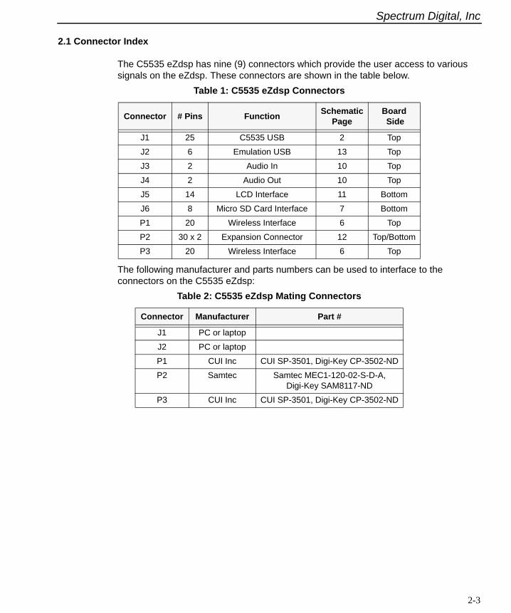
2.1 Connector Index
The C5535 eZdsp has nine (9) connectors which provide the user access to varioussignals on the eZdsp. These connectors are shown in the table below.
The following manufacturer and parts numbers can be used to interface to theconnectors on the C5535 eZdsp:
Table 1: C5535 eZdsp Connectors
Connector # Pins Function SchematicPage
Board Side
J1 25 C5535 USB 2 Top
J2 6 Emulation USB 13 Top
J3 2 Audio In 10 Top
J4 2 Audio Out 10 Top
J5 14 LCD Interface 11 Bottom
J6 8 Micro SD Card Interface 7 Bottom
P1 20 Wireless Interface 6 Top
P2 30 x 2 Expansion Connector 12 Top/Bottom
P3 20 Wireless Interface 6 Top
Table 2: C5535 eZdsp Mating Connectors
Connector Manufacturer Part #
J1 PC or laptop
J2 PC or laptop
P1 CUI Inc CUI SP-3501, Digi-Key CP-3502-ND
P2 Samtec Samtec MEC1-120-02-S-D-A,Digi-Key SAM8117-ND
P3 CUI Inc CUI SP-3501, Digi-Key CP-3502-ND
2-3

Spectrum Digital, Inc
2.1.1 J1, C5535 USB Connector
The USB connector, J1, is attached the C5535 processor for use by C5535 softwareapplications. The signals on the pins of this connector are shown below.
2.1.2 J2, XDS100 USB Connector
The USB connector, J2, is used to attach the C5535 eZdsp to a personal computer orlaptop. This allows the user to develop and debug software on the C5535 eZdsp. Thesignals on the pins of this connector are shown below.
Table 3: J1, USB Connector
Pin # Signal Name
1 USBVDD
2 D-
3 D+
4 ID / NC
5 USBVSS/GND
6,7,8,9 GND (shield)
Table 4: J2, XDS100 USB Connector
Pin # Signal Name
1 U7, Pin 1 (VCC), VCCUSB, 5V_USB
2 U7, Pin 5 (IO4), U6, Pin 7(DM), D-
3 U7, Pin 3(IO1), U6, Pin 8(DP), D+
4 GND
5 GND, shield
6 GND, shield
2-4 TMS320C5535 eZdsp Technical Reference Manual

Spectrum Digital, Inc
2.1.3 J3, Audio In Connector
The Stereo In connector, J3, is used to bring signals into the TLV320AIC3204 codec,U17. The signals on the pins of this connector are shown below.
The figure below shows a typical stereo jack.
Table 5: J3, Audio In Connector
Pin # Signal Name AIC3204 Pin #
1 GND-AIC
2 AIC_LINE2L U17, Pin 15
3 AIC_LINE2R U17, Pin 16
4 No connect
5 No connect
Figure 2-3, Audio In JackLeft Line In
Ground
Right Line In
2-5

Spectrum Digital, Inc
2.1.4 J4, Audio Out Connector
The Audio Out connector, J4, is used to bring signals from the TLV320AIC3204 codec,U17. The signals on the pins of this connector are shown below.
The figure below shows a typical headphone jack.
Table 6: J4, Audio Out Connector
Pin # Signal Name AIC3204 Pin #
1 GND-AIC
2 HEADPHONE_LOUT U17, Pin 25
3 HEADPHONE_ROUT U17, Pin 27
4 No connect
5 No connect
Left Line In
Ground
Figure 2-4, Audio Out Jack
Right Line In
2-6 TMS320C5535 eZdsp Technical Reference Manual

Spectrum Digital, Inc
2.1.5 J5, LCD Interface
Connector, J5, is used to interface to an LCD character display. The signals on the pinsof this connector are shown below.
2.1.6 J6, Micro SD Card Connector
The Micro SD connector, J6, is used to interface the C5535 processor to a micro SDcard. The signals on the pins of this connector are shown below.
Table 7: J5, LCD Interface
Pin # Signal Name
1 C2P2 C2N3 C1P4 C1N5 VBAT6 VBREF7 VSS, GND8 VDD, VCC_3V39 RESn, TARGET_PWR_GOOD10 SCL, I2C_SCL11 SDA, I2C_SDA12 IREF13 VCOMH14 VCC, V13
Table 8: J6, Micro SD Card Connector
Pin # Signal Name
1 DAT2, SD_DATA2
2 DAT3, SD_DATA3
3 CMD, SD_CMD
4 VDD, VCC_3V3
5 CLK, SD_CLK
6 GND
7 DAT0, SD_DATA0
8 DAT1, SD_DATA1
9 INSERT, VCC_3V3
10 INSERT_COM, GND
11,12,13,14 NC
2-7

Spectrum Digital, Inc
2.1.7 P1, P3, Wireless Interface
Connectors P1 and P3 are used to provide an interface to Texas Instruments WirelessInterface modules. The signals on the pins of these connectors are shown in the tablesbelow.
Table 9: P1, Wireless Interface Connector
Pin # Signal Name Pin # Signal Name
1 GND 2 SD_DATA0
3 UART_RTS 4 SD_DATA1
5 RTC_CLKOUT 6 SD_DATA2
7 UART_TX 8 SD_DATA3
9 UART_RX 10 GPIO10
11 I2C_SDA 12 GPIO11
13 I2C_SCL 14 SPI_CS2
15 SD_CLK 16 SPI_CLK
17 SD_CMD 18 SPI_TX
19 GND 20 SPI_RX
Table 10: P3, Wireless Interface Connector
Pin # Signal Name Pin # Signal Name
1 NC 2 GND
3 NC 4 NC
5 NC 6 NC
7 VCC_3V3 8 I2S1_RX
9 VCC_3V3 10 I2S1_DX
11 I2S1_FS 12 NC
13 GPIO12 14 NC
15 GPIO14 16 NC
17 I2S1_CLK 18 UART_CTS
19 GPIO14 20 GPIO13
2-8 TMS320C5535 eZdsp Technical Reference Manual

Spectrum Digital, Inc
2.1.8 P2, Expansion Connector
The expansion edge connector, P2, provides the C5535 serial interface signals tolimitless user expansion boards. This edge connector has all of the odd number(1,3,...,59) tabs on the top side of the board and all of the even number tabs (2,4,...,46)on the bottom side of the board. The diagram below shows the position of these tabs.
Top Side View
Pin 1
Pin 19Pin 23
Pin 59
Key
Pin 2
Pin 20Pin 24
Pin 60Bottom Side View
Figure 2-5, P2 Connector Tab Positions
2-9

Spectrum Digital, Inc
The table below lists the signals that appear on each of the tabs of connector P2. Thesignals on the pins of this connector are shown below.
Table 11: P2, Expansion Connector
Pin #Top Signal Name Pin #
Bottom Signal Name
1 GND 2 GND
3 SPI_CS1 4 GPIO13
5 SPI_CLK 6 GPIO12
7 SPI_TX 8 GPIO14
9 SPI_RX 10 GPIO15
11 GND 12 GND
13 GND 14 GND
15 GND 16 GND
17 I2C_SDA 18 GPIO16
19 I2C_SCL 20 GPIO17
Key Key
23 I2S2_CLK 24 GPIO11
25 I2S2_RX 26 GPIO10
27 I2S2_DX 28 GPIO5
29 I2S2_FS 30 GPIO4
31 GND 32 GND
33 I2S1_CLK 34 UART_RTS
35 I2S1_RX 36 UART_CTS
37 I2S1_DX 38 UART_RX
39 I2S1_FS 40 UART_TX
41 VCC_3V3 42 VCC_USB_DUAL
43 VCC_3V3 44 VCC_USB_DUAL
45 I2S0_CLK 46 SPI_CS3
47 I2S0_RX 48 VCC_USB_DUAL
49 I2S0_DX 50 GPAIN3
51 I2S0_FS 52 GPAIN2
53 SPI_CS2 54 GPAIN1
55 SPI_CS0 56 GPAIN0
57 VCC_3V3 58 VCC_USB_DUAL
59 VCC_3V3 60 VCC_USB_DUAL
2-10 TMS320C5535 eZdsp Technical Reference Manual

Spectrum Digital, Inc
2.2 System LEDs
The C5535 eZdsp has 6 Light Emitting Diodes (LED). LEDs DS2- DS6 are under theapplication software control running on the C5535 processor. The C5535 eZdsp LEDsare shown in the table below.
2.3 Switches
The C5535 eZdsp has three switches, two push button switches, and one DIPswitch. These switches are shown in the table below.
2.3.1 SW1, SW2, Momentary Push Button Switches
Switches SW1, and SW2 are momentary push button switches read by the applicationsoftware running on the C5535 processor using the GPAIN1 port.
Table 12: System LEDs
LED # Color SchematicPage Signal Name
DS1 Green 13 U6, Pin 60, PWREN#
DS2 Green 2 U4, Pin J3, XF
DS3 Green 11 U4, Pin P8, GPIO17
DS4 Red 11 U4, Pin P3, GPIO16
DS5 Yellow 11 U4, Pin N7, GPIO15
DS6 Blue 11 U4, Pin P2, GPIO14
Table 13: Switches
Switch # SchematicPage Signal Name/Reading
SW1 only closed 11 GPAIN1, approximately 1.2 volts
SW2 only closed 11 GPAIN1, approximately 0.9 volts
SW3 5 4 position DIP switch
2-11

Spectrum Digital, Inc
2.3.2 SW3, 4 Position DIP Switch
Switch SW3 is a 4 position DIP switch. The signals attached to each position are shownin the table below.
The figure below shows switch SW3 default settings.
The table below shows the functions of the setting in each position of SW3.
* Note: GPIO15 can overwrite
Table 14: Switch SW3
Position Signal Name Default Setting
1 CLK_SEL OFF
2 UART_BUFF_EN ON
3 AIC3204I2C_ENn OFF
4 SPI_CS0 ON
Table 15: Switch SW3 Functions
Position Setting Function
1ON Select external 12 MHz. clock
OFF Select internal 32 MHz. RTC clock
2ON * Enable UART via J2 for VCP
OFF * Disable UART via J2
3ON Disable AIC3204 interface
OFF Enable AIC3204 interface
4ON Enable SPI Flash CS
OFF Disable SPI Flash CS
Figure 2-6, Switch SW3, Default Settings
1st positionSW
3
RaisedActuator
2-12 TMS320C5535 eZdsp Technical Reference Manual

Spectrum Digital, Inc
2.4 Jumpers
The C5535 eZdsp has 7 jumpers. The location of the jumpers are shown in the figurebelow.
The function of these jumpers is shown in the table below.
Jumper JP2 is the power source select jumper. When this jumper is shorted theC5535 eZdsp can be powered from the C5535 USB interface (J1). This jumper isshipped in the “shorted” state from the factory.
Table 16: Jumpers
Jumper # of positions
SchematicPage Jumper Function
JP1 2 4 Allows measurement of VCore
JP2 2 13Power source select. Allows connection of
VCCUSB to VBUS_C5515
JP3 3 9 I2C Headers
JP4 2 4 Allows measurement of VDD_IO1 voltage
JP5 2 8 Allows measurement of USB 3.3V
JP6 2 10 Allows measurement of VCC_3V3 for AIC3204
JP7 2 10 Allows measurement of V3.3A for AIC3204
Figure 2-7, C5535 eZdsp Jumpers
JP1
JP2
JP3
JP4 JP5
JP6
JP7
2-13

Spectrum Digital, Inc
2.5 Test Points
The C5535 eZdsp has seven (7) test points for the monitoring of signals. The locationof the test points are shown in the figure below.
The signals on the test points are shown in the table below.Table 17: Test Points
TP # SchematicPage Signal Name
TP1 4 GND
TP2 8 VCC_1V8_TP
TP3 2 U4, Pin I14, VBUS/VBUS_C5535
TP4 2 U4, Pin A2, CLKOUT
TP5 8 VCC_3V3_TP
TP6 10 GND
TP7 9 U11, Pin 7,8, VCC_1V3, VCC_1V3_TP
Figure 2-8, C5535 eZdsp Test Points
TP1
TP2 TP3
TP4
TP5
TP6
TP7
2-14 TMS320C5535 eZdsp Technical Reference Manual

Appendix A
Schematics
This appendix contains the schematics for the TMS320C5535 eZdsp.
A-1

Spectrum Digital, Inc5 5
4 4
3 3
2 2
1 1
DD
CC
BB
AA
Siz
e:
Dat
e:
DW
G N
OR
evis
ion:
She
eto
f
Title
:
Pag
e C
onte
nts:
C
SP
EC
TRU
M D
IGIT
AL
INC
OR
PO
RA
TED
5145
82-0
001
Tues
day,
Jul
y 26
, 201
11
13
B
TMS
320C
5535
EZD
SP
MO
DU
LE
TITL
E S
HE
ET
4. ALL 0.1 uF AND 0.01uF CAPACITORS ARE DECOUPLING CAPS UNLESS
OTHERWISE NOTED. THEY ARE SHOWN
ON THE PAGE WITH THE INTEGRATED
CIRCUITS THEY SHOULD BE PLACED NEAR.
NOTES, UNLESS OTHERWISE SPECIFIED:
1. RESISTANCE VALUES IN OHMS.
2. CAPACTITANCE VALUES IN MICROFARADS.
3. REFERENCE DESIGNATORS USED:
SCHEMATIC
CONTENTS
01 - TITLE PAGE
02 - TMS320C5535 IO
03 - UART BUFFER
04 - TMS320C5535 POWER
05 - SPI FLASH
06 - CC BOARD INTERFACE
07 - MICRO SD INTERFACE
08 - POWER SUPPLIES
09 - AUDIO CODEC
10 - LCD/USER LEDS/SWITCHES
11 - EXPANSION CONNECTOR
12 - XDS100-v2 INTERFACE
SHEET
SHEET
SHEET
SHEET
REV
REV
REV
REV
ENGR
2
REVISION STATUS OF SHEETS
1
DATE
DATE
ENGR-MGR
MFG
7
DWN
DATE
8
DATE
DATE
CHK
RLSE
APPLICATION
35
NEXT ASSY
DATE
6
DATE
9
QA
USED ON
4
BA
AA
R.R.P.
T.W.K.
R.R.P.
R.R.P.
C.M.D.
R.R.P.
R.R.P.
10/15/2009
10/15/2009
10/15/2009
10/15/2009
10/15/2009
10/15/2009
10/15/2009
CA
AA
A
10
11
12
A
AA
Initial schematic for layout
DESCRIPTION
REV
APPROVED
DATE
1/10/2011
RRP
A
BETA
UPDATES
6/19/2011
RRP
B
PRODUCTION UNITS
7/19/2011
RRP
C
A-2 TMS320C5535 eZdsp Technical Reference Manual

Spectrum Digital, Inc
5 5
4 4
3 3
2 2
1 1
DD
CC
BB
AA
GP
AIN
2G
PA
IN1
GP
AIN
0
GP
AIN
3
TAR
GE
T_E
MU
1
TAR
GE
T_E
MU
0
CLK
IN
US
B_X
I
US
B_V
BU
S
US
B_D
MU
SB
_DP
I2C
_SC
LI2
C_S
DA
SP
I_C
S0
SP
I_C
S1
SP
I_C
LK
SP
I_C
S2
SP
I_C
S3
UA
RT_
RX
UAR
T_C
TSU
ART_
RTS
UAR
T_TX
GP
IO12
GP
IO13
GP
IO14
GP
IO15
GP
IO16
GP
IO17
I2S
2_C
LKI2
S2_
FSI2
S2_R
XI2
S2_D
X
SPI
_RX
SPI_
TX
I2S1
_DX
I2S
1_FS
I2S
1_C
LK
I2S1
_RX
GP
IO10
GP
IO11
SD
_DAT
A1
SD
_DAT
A0
SD
_CM
DS
D_C
LK
SD
_DAT
A3
SD
_DAT
A2
WA
KE
UP
RTC
_CLK
OU
T
CLK
OU
T
SD
_DA
TA1
SD
_DA
TA0
SD
_CM
DS
D_C
LK
SD
_DA
TA3
SD
_DA
TA2
CLK
_SE
L
VD
D_I
O1
VD
D_I
O1
VC
C_3
V3_
US
B
VC
C_1
V3
VB
US
_C55
35
VD
D_I
O1
VD
D_I
O1
GP
AIN
312
GP
AIN
212
GP
AIN
111
,12
TAR
GE
T_P
WR
_GO
OD
9,10
,11,
13
TAR
GET
_TM
S13
TAR
GET
_TR
STn
13
TAR
GE
T_TD
I13
TAR
GE
T_TD
O13
TAR
GE
T_TC
K13
CP
U_C
LK_1
2MH
Z10
US
B_C
LK_1
2MH
Z10
I2C
_SD
A6,
9,10
,11,
12I2
C_S
CL
6,9,
10,1
1,12
SP
I_C
S312
SP
I_C
S26,
12
UA
RT_
RX
3,6,
12U
AR
T_C
TS3,
6,12
UA
RT_
RTS
3,6,
12
UAR
T_TX
3,6,
12
I2S
2_D
X10
,12
I2S
2_FS
10,1
2I2
S2_
CLK
10,1
2
I2S
2_R
X10
,12
SP
I_C
S05,
12
SP
I_C
LK5,
6,12
SP
I_R
X5,
6,12
SPI_
TX5,
6,12
SP
I_C
S112
GP
IO17
11,1
2G
PIO
1611
,12
GP
IO15
3,11
,12
GP
IO14
6,11
,12
GP
IO12
6,11
,12
GP
IO13
6,12
I2S
1_D
X6,
12I2
S1_
FS6,
12I2
S1_
CLK
6,12
I2S
1_R
X6,
12G
PIO
106,
12G
PIO
116,
12
SD
_DA
TA2
6,7
SD
_DA
TA3
6,7
SD
_DA
TA0
6,7
SD
_CLK
6,7
SD
_CM
D6,
7
SD
_DA
TA1
6,7
RTC
_CLK
OU
T6
I2S
0_D
X12
I2S
0_FS
12I2
S0_
CLK
12
I2S
0_R
X12
GP
IO4
12G
PIO
512
GP
AIN
012 C
LK_S
EL5
Siz
e:
Dat
e:
DW
G N
OR
evis
ion:
She
eto
f
Title
:
Pag
e C
onte
nts:
B
SP
EC
TRU
M D
IGIT
AL
INC
OR
POR
ATE
D
5145
82-0
001
Frid
ay, J
uly
22, 2
011
213
B
TMS
320C
5535
EZD
SP
MO
DU
LE
GP
IO,M
MC
-SD
,SP
I,I2C
,I2S
R34
NO
-PO
P
R25 10K
TP3
VB
US
TP4
CLK
OU
T
R14 10
K
R22 10
K
R29
10K
1%
C84
0.1u
FR
59
10K
C82
0.1u
F
J1 US
BM
INI_
B
US
BVD
D1
D+
3D
-2
US
BVS
S5
ID4
SH
IELD
16
SH
IELD
27
SH
IELD
38
SH
IELD
49
FB
7
BLM
18AG
601S
N1D
1206
12
R17
220
C83
1uF
R56
NO
-PO
P
C6
10uF
R41
100K
C25
10uF
R54
0
C77
0.1u
F
Y1
32.7
68K
Hz
14
23
DS
2LE
D_G
RN
R11
710
K
R55
0
C66
1000
pF
C91
33pF
C55
35
U4-
1
RS
V10
H1
RS
V11
E2
RS
V7E
1R
SV8
F1R
SV9
G1
RS
V12
G2
CLK
_SE
LD
1
CLK
INC
1
CLK
OU
TA2
EMU
0L2
EMU
1M
1
GPA
IN0
A8G
PAIN
1B8
GPA
IN2
A9G
PAIN
3A
10
I2C
_SC
LC
4I2
C_S
DA
A4
INT0
C2
INT1
B1
LCD
_EN
_RD
B/S
PI_C
LKL3
LCD
_CS0
_E0/
SPI_
CS
0L1
LCD
_CS
_E1/
SPI
CS
1M
2LC
D_R
W_W
RB/
SPI_
CS
2N
2LC
D_R
S/SP
I_C
S3
M5
LCD
_D[0
]/SP
I_R
XN
4LC
D_D
[1]/S
PI_
TXK
1
LCD
_D[1
0]/I2
S2_
RX
/GP
[20]
/SP
I_R
XP
9LC
D_D
[11]
/I2S
2_D
X/G
P[2
7]/S
PI_
TXP
11LC
D_D
[12]
/UA
RT_
RTS
/GP
[28]
/I2S
3_C
LKN
12LC
D_D
[13]
/UA
RT_
CTS
/GP
[29]
/I2S
3_FS
P12
LCD
_D[1
4]/U
AR
T_R
XD
/GP[
30]/I
2S3_
RX
P13
LCD
_D[1
5]/U
AR
T_TX
D/G
P[31
]/I2S
3_D
XM
11
LCD
_D[2
]/GP
[12]
J2LC
D_D
[3]/G
P[1
3]N
5LC
D_D
[4]/G
P[1
4]P
2LC
D_D
[5]/G
P[1
5]N
7LC
D_D
[6]/G
P[1
6]P
3LC
D_D
[7]/G
P[1
7]P
8
LCD
_D[8
]/I2S
2_C
LK/G
P[18
]/SPI
_CLK
P5
LCD
_D[9
]/I2S
2_FS
/GP[
19]/S
PI_C
S0N
10
RE
SET
ND
2
RTC
_CLK
OU
TA3
RTC
XI
A7
RTC
XO
A6
MM
C0_
CLK
/I2S
0_C
LK/G
P[0]
M8
MM
C0_
CM
D/I2
S0_
FS/G
P[1
]M
10M
MC
0_D
0/I2
S0_D
X/G
P[2]
J1M
MC
0_D
1/I2
S0_R
X/G
P[3]
P6
MM
C0_
D2/
GP
[4]
N13
MM
C0_
D3/
GP
[5]
P7
MM
C1_
CLK
/I2S
1_C
LK/G
P[6]
M14
MM
C1_
CM
D/I2
S1_
FS/G
P[7
]L1
1M
MC
1_D
0/I2
S1_D
X/G
P[8]
M13
MM
C1_
D1/
I2S1
_RX/
GP[
9]P
10M
MC
1_D
2/G
P[1
0]L1
2M
MC
1_D
3/G
P[1
1]M
12
TCK
N3
TDI
K2
TDO
N1
TMS
N6
TRS
TNP4
US
B_D
MJ1
4U
SB_
DP
H14
US
B_R
1G
14
US
B_V
BU
SL1
4
US
B_M
12X
IE
14
US
B_M
12X
OD
14
WAK
EU
PA5
XFJ3
VSS
_RTC
C5
CV
DD
_RTC
B4C
VD
D_R
TCB5
US
B_V
DD
OS
CE
13
US
B_V
SSO
SC
D12
USB
_VS
SR
EF
F12
DV
DD
_RTC
C3
R37
100K
R13 10
KR18
100K
R13
10
R13
00
R12
90
R38
0
R12
80
R69
0R
680
C90
33pF
C24
0.1u
FD
26.
2V
A-3

Spectrum Digital, Inc5 5
4 4
3 3
2 2
1 1
DD
CC
BB
AA
VC
C_3
V3
VC
C_3
V3
TRG
T_U
ART_
TX13
TRG
T_U
AR
T_R
X13
TRG
T_U
AR
T_R
TS13
TRG
T_U
AR
T_C
TS13
UA
RT_
RTS
2,6,
12U
ART_
TX2,
6,12
UA
RT_
CTS
2,6,
12U
AR
T_R
X2,
6,12
GP
IO15
2,11
,12
UA
RT_
BU
FF_E
N5
Siz
e:
Dat
e:
DW
G N
OR
evis
ion:
She
eto
f
Title
:
Pag
e C
onte
nts:
A
SP
EC
TRU
M D
IGIT
AL
INC
OR
PO
RA
TED
5145
82-0
001
Frid
ay, J
uly
22, 2
011
313
B
TMS
320C
5535
EZD
SP
MO
DU
LE
UA
RT
BU
FFE
R
R13
30
U5B
74C
BTLV
3125
PW
R
65
4
U5C
74C
BTL
V31
25P
WR
89
10
U5D
74C
BTL
V31
25P
WR
1112
13
R24
10K
U5A
74C
BTL
V31
25P
WR
32
17
14
C39 0.1u
F
A-4 TMS320C5535 eZdsp Technical Reference Manual

Spectrum Digital, Inc
5 5
4 4
3 3
2 2
1 1
DD
CC
BB
AA
DS
P_L
DO
_OU
T
RS
V6
US
B_L
DO
_OU
T_R
EG
LDO
_EN
LDO
_EN
DS
P_L
DO
_OU
T_R
EG
I2C
_SC
L_P
WR
I2C
_SD
A_P
WR
I2C
_SD
A_P
WR
I2C
_SC
L_P
WR
AG
ND
AG
ND
VC
C_3
V3_
US
B
VC
C_3
V3_
US
B
US
B_LD
O_O
UT
US
B_L
DO
_OU
T
AN
A_L
DO
_OU
T
AN
A_L
DO
_OU
T
AN
A_L
DO
_OU
T
AG
ND
AG
ND
AG
ND
AG
ND
AG
ND
AG
ND
AG
ND
VC
C_1
V8D
SP
_LD
O_O
UT_
RE
G
V_P
WR
_MO
N
DS
P_L
DO
_OU
T
VD
D_I
O1_
CP
UV
CC
_3V
3_P
WR
V_P
WR
_MO
N
VD
D_I
O1_
CP
UVC
C_1
V3
VC
C_1
V8
VC
C_1
V3
I2C
_SD
A_P
WR
8,9
I2C
_SC
L_P
WR
8,9
Siz
e:
Dat
e:
DW
G N
OR
evis
ion:
She
eto
f
Title
:
Pag
e C
onte
nts:
A
SP
EC
TRU
M D
IGIT
AL
INC
OR
PO
RA
TED
5145
82-0
001
Tues
day,
Jul
y 26
, 201
14
13
B
TMS
320C
5535
EZD
SP
MO
DU
LE
TMS
320C
5535
PO
WER
NO-POP
NO-POP
I2C ADDRESS
100 0000
I2C ADDRESS
100 0100
C51
0.01
uF
R60 0
R12
20
C48
0.1u
F
C75
0.1u
F
C67
0.1u
F
FB
4
BLM
18AG
601S
N1D
1206
12
C4
10uF
FB
5
BLM
18AG
601S
N1D
1206
12
C52
1uF
C43
0.01
uF
C53
1uF
C3
10uF
C57
0.1u
F
C29
0.1u
F
C87
0.1u
F
C63
0.1u
F
C27
0.1u
F C55
0.01
uF
U15
INA
219I
DC
N
VIN+1
VIN-2
GND 3
VS 4
SCL 5SDA 6
A0 7A1 8
C85
0.1u
F
C69
0.1u
F
C10
20.
1uF
R12
3N
O-P
OP
C59
0.1u
F
C46
0.1u
F
FB6
BLM
18AG
601S
N1D
1206
12
C5
1uF
C45
0.1u
F
C71
0.1u
F
R12
40
R20
1 1%
C73
0.01
uF
C55
35
U4-
2
LDO
IB1
0
AN
A_L
DO
OB
9
DS
P_L
DO
_EN
C13
RS
V6
B13
LDO
IB1
4
DS
P_L
DO
OA
13
RS
V3
B12
RS
V0
A12
LDO
IC
14
US
B_L
DO
OD
13
VD
DA_
ANA
B7
US
B_V
DD
1P3
E12
US
B_V
DD
1P3
F14
US
B_V
DD
1P3
K13
US
B_V
DD
PLL
G13
US
B_V
DD
A1P
3H
12
US
B_V
DD
A3P
3G
12
CV
DD
C11
CV
DD
D3
CV
DD
D11
CV
DD
F2C
VD
DG
3C
VD
DH
2C
VD
DK
11C
VD
DM
6C
VD
DM
9C
VD
DN
9
DVD
DIO
C6
DVD
DIO
L4D
VDD
IOM
3D
VDD
IOM
4D
VDD
ION
8D
VDD
ION
11D
VDD
ION
14
VSS
E3
RS
V1
K12
RS
V2
L13
VSS
A14
VSS
B2
VSS
B3
VSS
C8
VSS
C12
VSS
D4
VSS
D5
VSS
D10
VSS
E4
VSS
E11
VSS
F3VS
SH
3VS
SJ1
3VS
SK
3VS
SK
4VS
SL5
VSS
L10
VSS
M7
VSS
P1
VSS
P14
VS
SA_A
NA
B6
US
B_V
SS
1P3
K14
US
B_V
SS
PLL
F13
VS
SA_A
NA
C9
US
B_V
SS
A1P3
J12
US
B_V
SS
A3P3
H13
BG
_CAP
C10
VD
DA_
PLL
C7
VSS
A_P
LLA
1
RS
V4
A11
RS
V5
B11
C42
1uF
JP1
12
C62
0.1u
F
C32
0.1u
F
C88
0.1u
F
R61 0
C89
0.01
uF
FB1
BLM
18A
G60
1SN
1D1
2
R64 0
C74
1000
pF
C28
0.1u
F
L3
BLM
18AG
601S
N1D
1206
12
C49
0.1u
F
C64
1uF
C40
0.1u
F
TP1
GN
D
C30
0.1u
F
R62
NO
-PO
P
C65
0.1u
F
C54
1uF
R63
NO
-PO
P
C60
0.1u
F
JP4
12
C41
0.01
uF
C56
1000
pF
C2
1uF
C1
10uF
R97
1 1%C
38
0.01
uF
R12
1N
O-P
OP
C86
1uF
C72
0.1u
F
U3
INA
219I
DC
N
VIN+1
VIN-2
GND 3
VS 4
SCL 5SDA 6
A0 7A1 8
C50
1000
pF
A-5

Spectrum Digital, Inc5 5
4 4
3 3
2 2
1 1
DD
CC
BB
AA
SP
I_H
OLD
SPI_
TX
SPI_
CLK
SP
I_R
XS
PI_
WP
SP
I_C
S_S
W_I
NS
PI_
CS
_SW
_OU
T
SP
I_C
S0_
DE
Vn
SP
I_C
S_S
W_I
NS
PI_
CS
_SW
_OU
T
VC
C_3
V3
VD
D_I
O1
VD
D_I
O1
VD
D_I
O1
VD
D_I
O1
SPI_
TX2,
6,12
SP
I_R
X2,
6,12
SP
I_C
LK2,
6,12
CLK
_SEL
2U
AR
T_B
UFF
_EN
3A
IC32
04I2
C_E
Nn
10
SP
I_C
S0
2,12
Siz
e:
Dat
e:
DW
G N
OR
evis
ion:
She
eto
f
Title
:
Pag
e C
onte
nts:
C
SP
EC
TRU
M D
IGIT
AL
INC
OR
PO
RA
TED
5145
82-0
001
Tues
day,
Jul
y 26
, 201
15
13
B
TMS
320C
5535
EZD
SP
MO
DU
LE
SP
I FLA
SH
OR M25P64-VMF6TP
DIP
Switch Defaults:
CLK_SEL = OFF (pulled down)
UART_BUFF_EN = ON (pulled down)
AIC3204I2C_ENn = OFF (pulled down)
U9 W
25X
64V
SFIG
CS
7
DIO
15
GN
D10
VC
C2
HO
LD1
WP
9D
O8
SCLK
16
NC
.33
NC
.44
NC
.55
NC
.66
NC
.11
11
NC
.12
12
NC
.13
13
NC
.14
14
1 2 3 4
ONS
W3
DIP
_SW
ITC
H1 2 3 45678
R52
10K
R74
10K
R13
21K
R72
NO
-PO
P
R16
0
R33
10K
R12
0N
O-P
OP
R50
NO
-PO
P
R31
NO
-PO
P
R73
NO
-PO
P
R71
0
R51
NO
-PO
P
C81
0.1u
F
A-6 TMS320C5535 eZdsp Technical Reference Manual

Spectrum Digital, Inc
5 5
4 4
3 3
2 2
1 1
DD
CC
BB
AA
GP
IO10
GP
IO11
VC
C_3
V3
I2C
_SD
A2,
9,10
,11,
12I2
C_S
CL
2,9,
10,1
1,12
UAR
T_R
TS2,
3,12
UA
RT_
CTS
2,3,
12G
PIO
142,
11,1
2
RTC
_CLK
OU
T2
GP
IO12
2,11
,12
GP
IO13
2,12
UAR
T_TX
2,3,
12U
AR
T_R
X2,
3,12
SP
I_C
S2
2,12
SP
I_C
LK2,
5,12
SP
I_R
X2,
5,12
SPI_
TX2,
5,12
GPI
O10
2,12
GPI
O11
2,12
SD
_DA
TA2
2,7
SD
_DA
TA3
2,7
SD
_DA
TA0
2,7
SD
_CLK
2,7
SD
_CM
D2,
7
SD
_DA
TA1
2,7
I2S
1_D
X2,
12I2
S1_
FS2,
12
I2S
1_C
LK2,
12
I2S
1_R
X2,
12
Siz
e:
Dat
e:
DW
G N
OR
evis
ion:
She
eto
f
Title
:
Pag
e C
onte
nts:
A
SP
EC
TRU
M D
IGIT
AL
INC
OR
PO
RA
TED
5145
82-0
001
Frid
ay, J
uly
22, 2
011
613
B
TMS
320C
5535
EZD
SP
MO
DU
LE
CC
BO
AR
D IN
TER
FAC
E
NOTE: DIMENSIONS AND LOCATIONS OF THESE CONNECTORS MUST MEET SPECIFICATION FOR INTERFACE MODULES
P1
HE
AD
ER
10X
2
1 3 5 7 9 11 13 15 17 19
2 4 6 8 10 12 14 16 18 20
R79
33
R66
33
R80
33
R82
33R
6733
P3
HE
AD
ER
10X
2
1 3 5 7 9 11 13 15 17 19
2 4 6 8 10 12 14 16 18 20R
8133
A-7

Spectrum Digital, Inc5 5
4 4
3 3
2 2
1 1
DD
CC
BB
AA
SD
_DA
TA1
SD
_DA
TA0
SD
_CM
DS
D_D
ATA
3S
D_D
ATA
2
SD
_CLK
VC
C_3
V3
VC
C_3
V3
VC
C_3
V3
SD
_DA
TA2
2,6
SD
_DA
TA3
2,6
SD
_DA
TA0
2,6
SD
_CLK
2,6
SD
_CM
D2,
6 SD
_DA
TA1
2,6
Siz
e:
Dat
e:
DW
G N
OR
evis
ion:
She
eto
f
Title
:
Pag
e C
onte
nts:
A
SP
EC
TRU
M D
IGIT
AL
INC
OR
POR
ATE
D
5145
82-0
001
Frid
ay, J
uly
22, 2
011
713
B
TMS
320C
5535
EZD
SP
MO
DU
LE
MIC
RO
SD
CO
NN
EC
TOR
+C
15
10uF
R99
10K
R10
010
K
R10
910
K
R10
310
KR
9810
KR
102
10K
J6
Mic
roS
D_C
AR
D
DA
T32
CM
D3
VD
D4
CLK
5V
SS6
DA
T07
DA
T18
DA
T21
INS
ER
T9
INSE
RT_
CO
M10
11 111212
1313
1414
1515
C10
6
0.1u
F
R10
1N
O-P
OP
A-8 TMS320C5535 eZdsp Technical Reference Manual

Spectrum Digital, Inc
5 5
4 4
3 3
2 2
1 1
DD
CC
BB
AA
I2C
_SD
A_P
WR
I2C
_SC
L_P
WR
VC
C_3
V3
FTD
I_3V
3
VC
C_1
V8
VD
D_I
O1
VC
C_3
V3_
US
B
V_P
WR
_MO
N
VC
C_U
SB
_DU
AL
VC
C_U
SB
_DU
AL
VC
C_3
V3_
PWR
I2C
_SD
A_P
WR
4,9
I2C
_SC
L_P
WR
4,9
Siz
e:
Dat
e:
DW
G N
OR
evis
ion:
She
eto
f
Title
:
Pag
e C
onte
nts:
C
SP
EC
TRU
M D
IGIT
AL
INC
OR
POR
ATE
D
5145
82-0
001
Tues
day,
Jul
y 26
, 201
18
13
B
TMS
320C
5535
EZD
SP
MO
DU
LE
PO
WE
R M
AN
AGEM
EN
T
NO-POP
I2C ADDRESS
100 1000
Vout = Vref x ( 1 + Rtop/RBottom ) ; VREF = 0.6
Vout = Vref x ( 1 + Rtop/RBottom ) ; VREF = 0.6
Vout = 0.6 x ( 1 +4.47 )
Vout = 0.6 x ( 1 + 2 )
L62.
2uH
C10
10.
1uF
C97
.1uF
C23
4.7u
F
C12
5
2200
pF
C99
4.7u
F
R96
1 1%
C21
10uF
C10
04.
7uF
JP5
12
C22
.1uF
C94
10uF
C12
3
.1uF
R65
8.06
K 1
%
R2
0
U16
INA
219I
DC
N
VIN+1
VIN-2
GND 3
VS 4
SCL 5SDA 6
A0 7A1 8
R15
1.80
K 1
%
R11
90
R70
1.80
K 1
%
R1
0
R11
3.60
K 1
%
TP5
VC
C_3
V3_
TP
C12
4
2200
pF
U1 TP
S62
260D
DC
T
VIN
11
GN
D2
EN
3FB
4
SW5
TP2
VC
C_1
V8_
TP
U12
TPS
6226
0DD
CT
VIN
11
GN
D2
EN
3FB
4
SW
5
C20
4.7u
F
R11
80
L72.
2uH
A-9

Spectrum Digital, Inc5 5
4 4
3 3
2 2
1 1
DD
CC
BB
AA
I2C
_SC
L_P
WR
I2C
_SD
A_P
WR
VC
C_3
V3_P
WR
V_P
WR
_MO
N
VC
C_1
V3
VC
C_3
V3_
PW
R
VC
C_3
V3_
PW
R
I2C
_SD
A_P
WR
4,8
I2C
_SC
L_P
WR
4,8
I2C
_SD
A2,
6,10
,11,
12I2
C_S
CL
2,6,
10,1
1,12
TAR
GE
T_P
WR
_GO
OD
2,10
,11,
13
Siz
e:
Dat
e:
DW
G N
OR
evis
ion:
She
eto
f
Title
:
Pag
e C
onte
nts:
A
SP
EC
TRU
M D
IGIT
AL
INC
OR
POR
ATE
D
5145
82-0
001
Frid
ay, J
uly
22, 2
011
913
B
TMS
320C
5535
EZD
SP
MO
DU
LE
PO
WE
R M
AN
AGEM
EN
T
Pow
er M
onito
r I2
C P
robe
Poi
nt H
eade
rs
RF1 = ( Vout/Vref - 1) * RF2
RF1 = ( 1.3/1.224 - 1) * 169K
R12
5
10.7
K
+C
954.
7uF
R12
6
169K
1%
+C
264.
7uF
R12
7
220K
JP3
HE
AD
ER
3
1 2 3
R87
0
R83
NO
-PO
P
R85
NO
-PO
P
TP7
VC
C_1
V3_
TP
U11
TPS7
6601
IN1
5
GN
D3
EN
4FB
1
OU
T28
IN2
6O
UT1
7
PG
2
R86
0
C98
4.7u
F
R84
0
A-10 TMS320C5535 eZdsp Technical Reference Manual

Spectrum Digital, Inc
5 5
4 4
3 3
2 2
1 1
DD
CC
BB
AA
AIC
_LIN
E2L
AIC
_IIS
CLK
AIC
_IIS
FSA
IC_I
ISD
0A
IC_I
ISD
1
AIC
_MO
DE
_SE
L
AIC
_LIN
E2R
CO
NN
_HP
_LO
UT
CO
NN
_HP
_RO
UT
HE
ADP
HO
NE
_LO
UT
HE
AD
PH
ON
E_R
OU
T
I2C
_SC
L_A
ICI2
C_S
DA
_AIC
AIC
_RST
I2C
_SC
LI2
C_S
DA
V3.
3AV
CC
_3V3
VC
C_3
V3
V3.
3AV
CC
_3V
3
VC
C_1
V8
GN
D-A
IC
GN
D-A
IC
GN
D-A
IC
GN
D-A
IC
GN
D-A
IC
GN
D-A
IC
GN
D-A
IC
VC
C_1
V8
GN
D-A
IC
VC
C_3
V3
VC
C_3
V3
VC
C_3
V3
VC
C_3
V3
AIC
3204
I2C
_EN
n5
TAR
GE
T_PW
R_G
OO
D2,
9,11
,13
CLK
_12M
HZ
13
US
B_C
LK_1
2MH
Z2
CP
U_C
LK_1
2MH
Z2
I2C
_SD
A2,
6,9,
11,1
2I2
C_S
CL
2,6,
9,11
,12
I2S
2_R
X2,
12I2
S2_
DX
2,12
I2S2
_FS
2,12
I2S
2_C
LK2,
12
Siz
e:
Dat
e:
DW
G N
OR
evis
ion:
She
eto
f
Title
:
Pag
e C
onte
nts:
A
SP
EC
TRU
M D
IGIT
AL
INC
OR
PO
RA
TED
5145
82-0
001
Frid
ay, J
uly
22, 2
011
1013
B
TMS
320C
5535
EZD
SP
MO
DU
LE
CO
DE
C
Tie
Ana
log
Pow
er to
Dig
ital P
ower
thro
ugh
sing
lepo
int c
onne
ctio
n or
Fer
rite
Bea
d.
STEREO IN 1
HEADPHONES OUT
Select Internal LDO
I2C ADDRESS
001 1000
C10
8
0.1u
F
R10
80
C16
0.47
uF
R13
510
K
C10
40.
1uF
JP6
12
J3 SJ1
-351
5-S
MT,
5P
JAC
K S
TER
EO
2 3 14 5
8
9
C17
0.47
uF
FB2
BLM
21A
G15
1SN
1D1
2
C11
7
0.1u
F
JP7
12
+
C13
100u
F
R10
7N
O-P
OP
R93
0
C10
5
0.1u
F
R13
8
10K
R11
01K
R9
NO
-PO
P
C12
10uF
R94
0
R10
6N
O-P
OP
+
C14
100u
F
C18
10uF
U17
TLV
320A
IC32
04IR
HB
T
BC
LK2
WC
LK3
DIN
4
IOVSS 7IN
1_L
13IN
1_R
14IN
2_L
15IN
2_R
16IN
3_L
20
MIC
BIAS
19
IN3_
R21
LDO_IN26
HP
L25
DVSS 28
LOR
23
AVDD24
RE
SE
T31
MC
LK1
DO
UT
5
IOVDD6
SC
L/S
SZ
9SD
A/M
OS
I10
AVSS 17
LOL
22H
PR
27
DVDD29 SC
LK/M
IC_D
ET
8M
ISO
11S
PI_
SE
L12
RE
F18
LDO
_SE
L30
GPI
O32
PPAD 33
R14
1
no-p
op
R11
11K
R92
0
C11
10uF
C8
10uF
R90
0
C12
2
.1uF
R7
100
C11
6
0.1u
F
R95
0
J4
SJ1
-351
5-S
MT,
5P
JAC
K S
TER
EO
2 3 14 5
8
9
C11
1
0.1u
F
R91
0
FB3
BLM
21A
G15
1SN
1D1
2
R10
4.7K
R10
44.
7K
C19
10uF
R13
610
K
U14
AS
DM
1-12
.000
MH
Z-LC
-T
OFF
n1
GN
D2
VC
C4
CLK
3
TP6
GN
D
U18
SN74
CBT
LV32
45A
PW
R
1B18
7A8
2B17
4A5
3B16
4B15
8A9
NC
1
1A2
OE
19
5A6
2A3
3A4
6A7
VC
C20
GN
D10
5B14
6B13
7B12
8B11
R8
0
R5
0
R13
7
220K
R13
410
K
R89
0
A-11

Spectrum Digital, Inc5 5
4 4
3 3
2 2
1 1
DD
CC
BB
AA
LED
1
LED
2
LED
3
LED
0
VC
C_3
V3
VC
C_3
V3
VC
C_3
V3
VC
C_3
V3
V13
AN
A_L
DO
_OU
T
VC
C_U
SB
_DU
AL
GP
IO12
2,6,
12
I2C
_SD
A2,
6,9,
10,1
2
I2C
_SC
L2,
6,9,
10,1
2
TAR
GET
_PW
R_G
OO
D2,
9,10
,13
GP
AIN
12,
12
GP
IO17
2,12
GP
IO16
2,12
GP
IO15
2,3,
12
GP
IO14
2,6,
12
Siz
e:
Dat
e:
DW
G N
OR
evis
ion:
She
eto
f
Title
:
Pag
e C
onte
nts:
A
SP
EC
TRU
M D
IGIT
AL
INC
OR
PO
RA
TED
5145
82-0
001
Frid
ay, J
uly
22, 2
011
1113
B
TMS
320C
5535
EZD
SP
MO
DU
LE
LCD
INTE
RFA
CE
LCD POWER 13V
0SD9616GLBBG01
J5 FCI_
1005
1922
-141
0ELF
C2P
1
C2N
2
C1P
3
C1N
4
VB
AT5
VB
RE
F6
VD
D8
VS
S7
RE
Sn
9
SC
L10
SD
A11
IREF
12
VC
OM
H13
VC
C14
U10
DS
N74
LV12
5
1112
13
C11
3.1
uF
C11
8.1
uF
L22.
2uH
SW
2
US
ER
2
14
32
C96
.1uF
C10
10uF
C10
3
10pF
U10
BS
N74
LV12
5
65
4
C11
92.
2uF
R11
620
K
C10
7
1uF
DS
6LE
D B
LUE
R11
310
K
R11
410
0
D1
MB
R05
20
R3
10K
SW
1
US
ER
1
14
32
R76
220
U13
TPS
6104
1
SW
1
GN
D2
FB3
EN
4
Vin
5
C12
02.
2uF
C11
0
1uF
R11
510
K
R75
220
C11
21u
F
DS
5LE
D Y
ELL
OW
C11
5
.022
uF
C10
9
1uF
R4
180K
1%
R77
220
R6
1.6M
1%
C12
1N
O-P
OP
DS
4LE
D R
ED
R11
239
2K 1
%
R10
5N
O-P
OP
C11
41u
F
U10
AS
N74
LV12
5
32
17
14
C9
10uF
,16V
U10
CS
N74
LV12
5
89
10
DS
3LE
D G
RN
R88
0
R78
220
A-12 TMS320C5535 eZdsp Technical Reference Manual

Spectrum Digital, Inc
5 5
4 4
3 3
2 2
1 1
DD
CC
BB
AA
GP
IO15
GP
IO14
GP
IO12
GP
IO13
SP
I_C
S1
SP
I_R
XSP
I_TX
SP
I_C
LK
I2C
_SD
AI2
C_S
CL
GP
IO16
GP
IO17
UA
RT_
RTS
UA
RT_
CTS
UA
RT_
RX
UAR
T_TX
I2S
2_C
LK
I2S
2_FS
I2S
2_R
XI2
S2_
DX
SP
I_C
S0
SP
I_C
S2
SP
I_C
S3
I2S
0_D
XI2
S0_F
S
I2S
0_C
LKI2
S0_
RX
GP
IO10
GP
IO11
I2S
1_D
XI2
S1_
FS
I2S
1_C
LKI2
S1_
RX
VC
C_3
V3
VC
C_U
SB
_DU
AL
GP
IO15
2,3,
11G
PIO
142,
6,11
GP
IO12
2,6,
11G
PIO
132,
6S
PI_C
S1
2
SP
I_R
X2,
5,6
SPI_
TX2,
5,6
SP
I_C
LK2,
5,6
I2C
_SD
A2,
6,9,
10,1
1I2
C_S
CL
2,6,
9,10
,11
GP
IO16
2,11
GP
IO17
2,11U
ART_
RTS
2,3,
6U
ART_
CTS
2,3,
6U
AR
T_R
X2,
3,6
UAR
T_TX
2,3,
6
I2S
2_D
X2,
10I2
S2_
FS2,
10
I2S
2_C
LK2,
10I2
S2_
RX
2,10
GP
AIN
02
GP
AIN
12,
11G
PA
IN2
2G
PA
IN3
2
SPI
_CS
02,
5S
PI_C
S2
2,6
SP
I_C
S3
2
I2S
0_D
X2
I2S
0_FS
2
I2S
0_C
LK2
I2S
0_R
X2
GP
IO4
2G
PIO
52
GP
IO10
2,6
GP
IO11
2,6
I2S
1_D
X2,
6I2
S1_
FS2,
6
I2S
1_C
LK2,
6I2
S1_
RX
2,6
Siz
e:
Dat
e:
DW
G N
OR
evis
ion:
She
eto
f
Title
:
Pag
e C
onte
nts:
A
SP
EC
TRU
M D
IGIT
AL
INC
OR
PO
RA
TED
5145
82-0
001
Frid
ay, J
uly
22, 2
011
1213
B
TMS
320C
5535
EZD
SP
MO
DU
LE
EX
PA
NS
ION
CO
NN
EC
TOR
S
P2
ED
GE
CO
NN
30X
2
2468101214161820242628303234363840
13579111315171923252729313335373942445254 4648505658
47 45 414351535557 49
6059
A-13

Spectrum Digital, Inc
FT1.
8V
PW
R_D
ET
SRST
_N_I
N
RTC
K
TAR
GET
_TM
S
TAR
GET
_TD
O
TAR
GE
T_TD
I
TARG
ET_T
CK
TMS
TRST
N
TDO
DIS
TDI
TCK
TARG
ET_T
RSTn
PW
R_R
ST
SR
ST_
N_O
UT
VC
CU
SB E
EC
SE
ESK
EED
ATA
XTIN
FTD
I_3V
3
FTD
I_3V
3
FTD
I_3V
3
FT1.
8V
FTD
I_3V
3
FTD
I_3V
3
FTD
I_3V
3
VB
US
_C55
35V
CC
US
B
VC
C_U
SB
_DU
AL
VC
C_U
SB
_DU
AL
TAR
GET
_TC
K2
TAR
GE
T_TM
S2
TAR
GET
_TR
STn
2
TAR
GE
T_TD
O2
TAR
GE
T_TD
I2
TAR
GE
T_P
WR
_GO
OD
2,9,
10,1
1
CLK
_12M
HZ
10TR
GT_
UAR
T_TX
3TR
GT_
UA
RT_
RX
3
TRG
T_U
AR
T_R
TS3
TRG
T_U
AR
T_C
TS3
Siz
e:
Dat
e:
DW
G N
OR
evis
ion:
She
eto
f
Title
:
Pag
e C
onte
nts:
A
SP
EC
TRU
M D
IGIT
AL
INC
OR
PO
RA
TED
5145
82-0
001
Frid
ay, J
uly
22, 2
011
1313
B
TMS
320C
5535
EZD
SP
MO
DU
LE
XD
S10
0-V
2 IN
TER
FAC
E
LOCA
TE L
ED A
LON
G A
BO
ARD
EDG
E SO
IT W
ILL
BE M
ORE
VISI
BLE.
EMU_
ENEM
U0
EMU1
OPT
IONA
L: IF
NO
T US
ED C
ONN
ECT
PWR_
GO
OD
TO P
WR_
DET.
Mounting holes 0.250 pad 0.125 drill
PLACE BY C5535 USB CONNECTOR
PLACE BY EMU USB CONNECTOR
C44
4.7u
F
R21
2K2
C7
10uF
JP2
CON2
12
C47
100n
F
C70
100n
F
C35
100n
F
C37
10nF
C78
.1uF
R39
47
R44
10K
C80
100n
F
R36
10K
R45
47-N
OP
OP
J2
USB
-A P
LUG
5V_U
SB
1
D+
3D
-2
GN
D4
S25 S1 6
R26
NO
-PO
P
R47
47
U2
93C
46_5
6_66
CS
1S
K2
DIN
3D
OU
T4
VC
C8
NC
17
NC
26
GN
D5
L5
BLM21P221SN
R23
0
C31
100n
F
C36
100n
F
C92
100n
F
C58
10nF
C61
100n
F
R49
47
L4
BLM21P221SN
L1
BLM
21P
221S
N
R43
10K
R30
0
C33
10nF
Z11
R27
0
Z21
R58
47
R28
12K
1%
C34
100n
F
U8
74LV
C1G
175-
DBV
6
CLK
1
GN
D2
D3
Q4
VC
C5
CLR
6
R32
0
U6
FT22
32H
L
XTO
UT
3
RE
SET
#14
EEC
S63
EES
K62
EED
ATA
61AGND 10
GND.1 1GND.2 5
TEST
13
VR
EG
OU
T49
VPHY4
VCORE.237 VCORE.112
DM
7D
P8
XTI
N2
GND.3 11GND.4 15
VCCIO.120VCCIO.231
AD
BU
S016
AD
BU
S117
AD
BU
S218
AD
BU
S319
AD
BU
S421
AD
BU
S522
AD
BU
S623
AD
BU
S724
AC
BU
S026
AC
BU
S127
AC
BU
S228
AC
BU
S329
AC
BU
S430
AC
BU
S532
AC
BU
S633
AC
BU
S734
BC
BU
S048
BC
BU
S152
BC
BU
S253
BC
BU
S354
BC
BU
S455
BC
BU
S557
BC
BU
S658
BC
BU
S759
PW
RE
N#
60S
US
PE
ND
#36
GND.5 25GND.6 35GND.7 47GND.8 51
VR
EG
IN50
RE
F6
VPLL9
VCORE.364
VCCIO.342VCCIO.456
BD
BU
S038
BD
BU
S139
BD
BU
S240
BD
BU
S341
BD
BU
S443
BD
BU
S544
BD
BU
S645
BD
BU
S746
C93
10nF
Z31
D3
MBR
0520
Z41
C79
100n
F
R57
10K
C68
100n
F
R35
0
D4
MB
R05
20
DS
1
GR
EE
N
R12
220
R19
10K
U7
TPD
2E00
1
VC
C1
NC
2
IO1
3
IO4
5
GN
D4
R48
47
R46
47-N
OP
OP
C76
4.7u
F
R40
NO
-PO
P
R53
47
R42
10K
A-14 TMS320C5535 eZdsp Technical Reference Manual

Appendix B
Mechanical Information
This appendix contains the mechanical information about theTMS320C5535 eZdsp produced by Spectrum Digital.
B-1

Spectrum Digital, Inc
THIS
DR
AWIN
G IS
NO
T TO
SC
ALE
ALL
ME
AS
UR
EM
EN
TS A
RE
IN IN
CH
ES
B-2 TMS320C5535 eZdsp Technical Reference Manual


Printed in U.S.A., August 2011
514585-0001 Rev. A