technical report mfis and tfft testing with the premier ii ... · technical report mfis and tfft...
TRANSCRIPT
Radiant Technologies, Inc.
2835D Pan American Freeway NE
Albuquerque, NM 87107
Tel: 505-842-8007
Fax: 505-842-0366
e-mail: [email protected]
Technical Report
MFIS and TFFT Testing with the Premier II Tester Rev C
Date: September 24, 2011
Author: Joe Evans
Introduction:
Since the successful implementation of thin-ferroelectric-film capacitors in IC memories,
work has turned to creating transistors with ferroelectric gates. The heart of the classic
field effect transistor is the capacitor formed by the linear dielectric oxide between the
gate electrode and the depletion region that forms in the substrate under the gate. If the
traditional oxide gate material could be replaced with a ferroelectric oxide, the transistor
would develop memory and open a new direction for technology and product
development. Functional thin-ferroelectric-film-transistors (TFFT) have been produced
by several organizations around the world. Work is also progressing for putting thin
ferroelectric films in the gate stack of silicon CMOS transistors (MFIS). The classic test
procedures for FETs are insufficient to evaluate transistors with memory. Fatigue,
imprint, retention, temperature shock, current hysteresis, and gate capacitor hysteresis all
require dedicated equipment under software control for efficient test execution.
Radiant created its first TFFTs in 1992 using 4/20/80 PNZT as the gate material and
indium oxide as the semiconductor. We developed a range of test procedures for these
devices using the RT66A Ferroelectric Tester. Six years later, when we began the design
of our present Precision family of testers, we ensured that the new tester architecture
would support test procedures that we planned to develop for piezoelectrics,
pyroelectrics, magnetoelectrics, and transistors.
Most Radiant testers now have an I2C communications port. Radiant’s recently
introduced its first accessory to connect to that port, the I2C DAC module. Multiple I
2C
DAC modules may be attached to a single port, providing Vision with the ability to set
and change multiple bias voltages during measurements. Please review the extensive
application note for the I2C DAC at http://www.ferrodevices.com/1/297/i2c_dac.asp.
The availability of extra voltage sources makes it possible for the Precision Premier II or
Precision Multiferroic to measure the performance of ferroelectric-gate transistors
Radiant Technologies, Inc. 2
(TFFTs and MFISs). This document explains the theory for such testing and gives
examples of such tests executed on Radiant’s SFRAM transistors.
Test Theory:
Transistors are three, four, or five terminal devices. During a single measurement, only
one of the five voltages is modulated while the others remain at a constant value.
Radiant’s ferroelectric capacitor testers have two primary terminals to match the two
terminals of a passive circuit component like a capacitor or a resistor. One terminal of
the tester, DRIVE, generates a voltage waveform while the other, RETURN, is an
electrometer. During transistor testing, the DRIVE output still provides the modulated
voltage stimulus while the RETURN input captures the current or charge generated by
the transistor. One or more I2C DACs provide the bias voltages required for the
transistor drain, substrate bias, and diffusion tub bias as required.
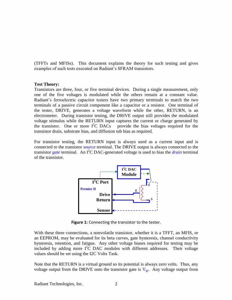
For transistor testing, the RETURN input is always used as a current input and is
connected to the transistor source terminal. The DRIVE output is always connected to the
transistor gate terminal. An I2C DAC-generated voltage is used to bias the drain terminal
of the transistor.
Figure 1: Connecting the transistor to the tester.
With these three connections, a nonvolatile transistor, whether it is a TFFT, an MFIS, or
an EEPROM, may be evaluated for its beta curves, gate hysteresis, channel conductivity
hysteresis, retention, and fatigue. Any other voltage biases required for testing may be
included by adding more I2C DAC modules with different addresses. Their voltage
values should be set using the I2C Volts Task.
Note that the RETURN is a virtual ground so its potential is always zero volts. Thus, any
voltage output from the DRIVE onto the transistor gate is Vgs. Any voltage output from
Premier II
Drive
Return
Sensor
I2C Port
I2C DAC
Module
s
d
g
Radiant Technologies, Inc. 3
the I2C DAC connected to the drain is Vds. Since the DRIVE and the I
2C DAC can
output both positive and negative voltages, any combination of tests may be constructed
using the Vision Library.
The dashed blue line in Figure 1 represents a connection from the drain of the transistor
to the SENSOR 1 input on the tester. With this connection, the tester can capture the
voltage on the drain of the transistor real time during a test. This connection can be
“T’d” from the output of the I2C DAC module but it will be on the transistor side of the
relay because the relay is inside the module. This will present no problem during
transistor testing. However, this connection should be removed to do gate measurements
because the cable can act as an antenna to inject noise into the RETURN input through
the channel when the channel is in the conductive state.
A traditional transistor curve tracer instrument biases the transistor gate, sweeps the drain
voltage, and measures the current through the transistor channel. This is called the Ids vs
Vds curve. Ferroelectric gate transistors require more characterization. The transistor
current conduction as a function of the gate voltage, Ids vs Vgs, will itself have a
hysteresis. Traditionally this trait is characterized on CMOS transistors using the C vs
Cox test where researchers attempt to predict the long term retention of MFIS transistors
using the memory window stability. Radiant offers a test procedure that will measure
that memory current characteristic directly. As well, a ferroelectric transistor will need to
be fatigued to test its reliability, changes in its programming voltages due to imprint will
need to be tracked over time, and, of course, data retention must be verified. All of these
tests may be executed using the Transistor Current Task in the Vision Library.
Transistors with non-linear gates exhibit complex behavior not typically experienced with
traditional transistors. It may be difficult to grasp the operation of the transistor tasks
described in this document without understanding the unique properties of a memory
transistor. Radiant’s SFRAM transistors will be used as example devices in this
application note to demonstrate real-world non-linear transistor characteristics.
SFRAM Transistors:
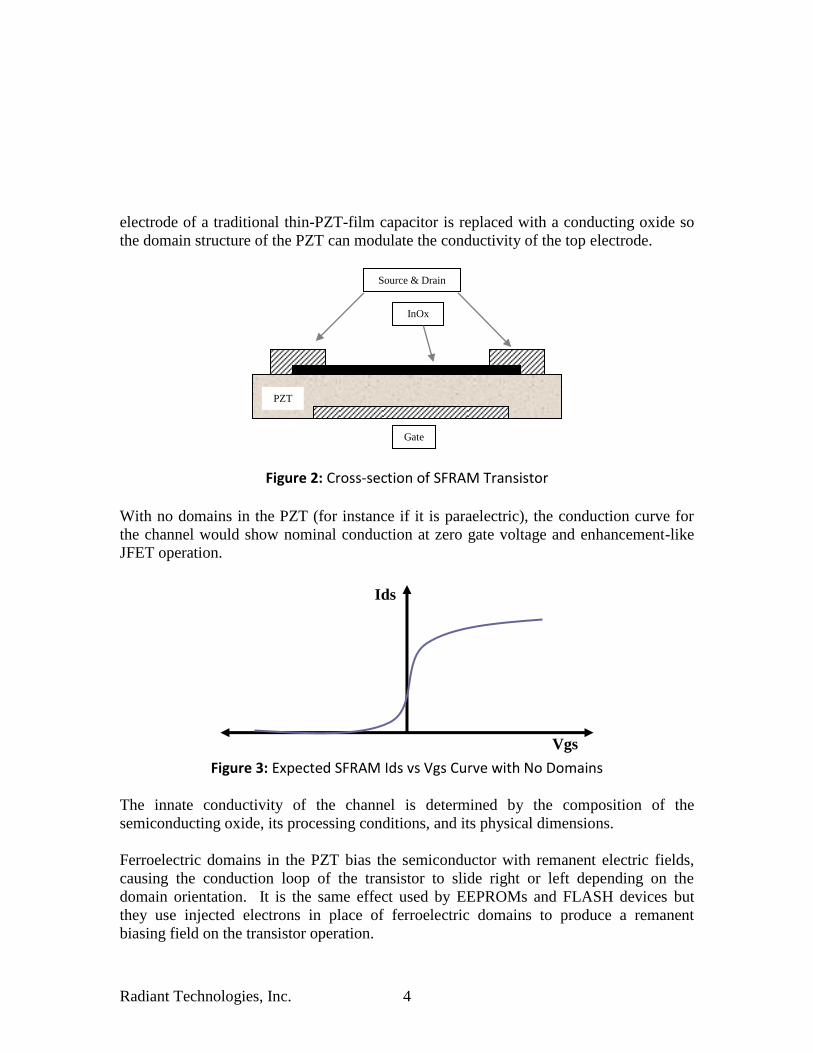
This is a short explanation of the SFRAM transistor. The SFRAM transistor is a thin film
transistor with a thin PZT gate oxide. There are a variety of configurations for TFFTs
made by universities and companies around the world. The acronym SFRAM stands for
Static Ferroelectric Random Access Memory. This name is a misnomer as an SFRAM is
not a RAM. It is a transistor constructed with an Indium Oxide (InOx) channel on a PZT
gate oxide. The gate electrode and the source/drains are platinum. Essentially, the top
Radiant Technologies, Inc. 4
electrode of a traditional thin-PZT-film capacitor is replaced with a conducting oxide so
the domain structure of the PZT can modulate the conductivity of the top electrode.
Figure 2: Cross-section of SFRAM Transistor With no domains in the PZT (for instance if it is paraelectric), the conduction curve for
the channel would show nominal conduction at zero gate voltage and enhancement-like
JFET operation.
Figure 3: Expected SFRAM Ids vs Vgs Curve with No Domains
The innate conductivity of the channel is determined by the composition of the
semiconducting oxide, its processing conditions, and its physical dimensions.
Ferroelectric domains in the PZT bias the semiconductor with remanent electric fields,
causing the conduction loop of the transistor to slide right or left depending on the
domain orientation. It is the same effect used by EEPROMs and FLASH devices but
they use injected electrons in place of ferroelectric domains to produce a remanent
biasing field on the transistor operation.
Ids
Vgs
PZT
InOx
Source & Drain
Gate
Radiant Technologies, Inc. 5
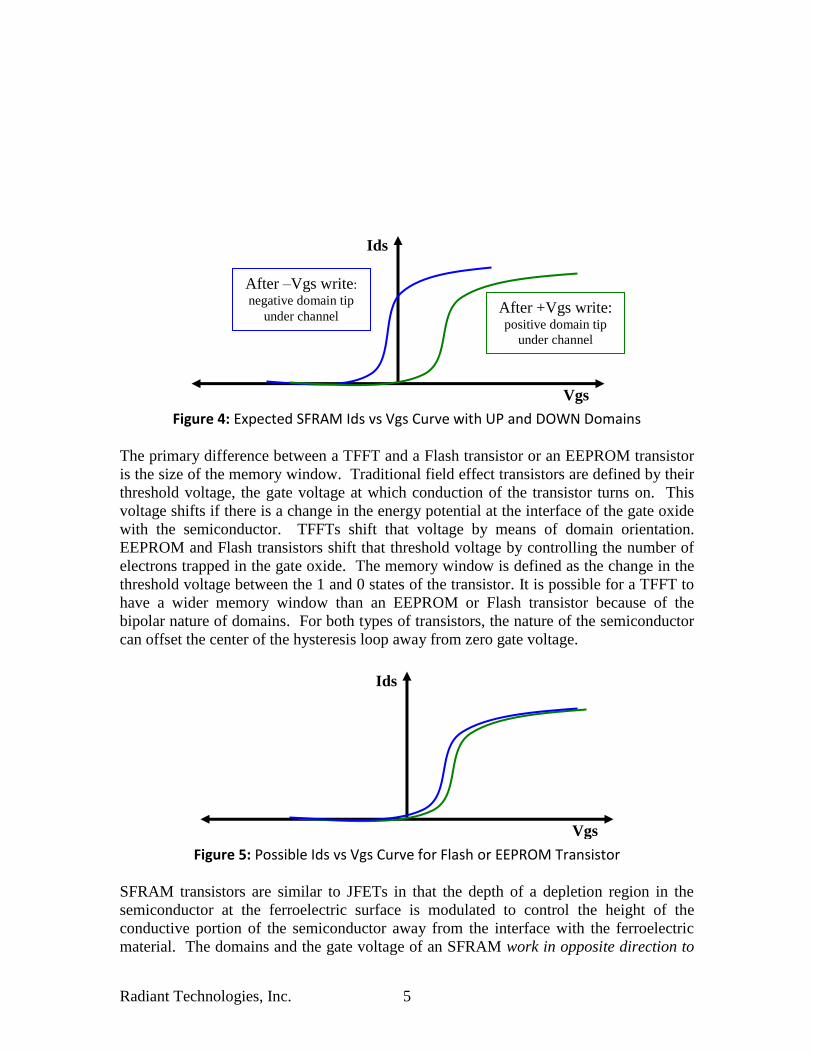
Figure 4: Expected SFRAM Ids vs Vgs Curve with UP and DOWN Domains
The primary difference between a TFFT and a Flash transistor or an EEPROM transistor
is the size of the memory window. Traditional field effect transistors are defined by their
threshold voltage, the gate voltage at which conduction of the transistor turns on. This
voltage shifts if there is a change in the energy potential at the interface of the gate oxide
with the semiconductor. TFFTs shift that voltage by means of domain orientation.
EEPROM and Flash transistors shift that threshold voltage by controlling the number of
electrons trapped in the gate oxide. The memory window is defined as the change in the
threshold voltage between the 1 and 0 states of the transistor. It is possible for a TFFT to
have a wider memory window than an EEPROM or Flash transistor because of the
bipolar nature of domains. For both types of transistors, the nature of the semiconductor
can offset the center of the hysteresis loop away from zero gate voltage.
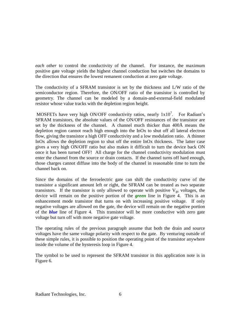
Figure 5: Possible Ids vs Vgs Curve for Flash or EEPROM Transistor
SFRAM transistors are similar to JFETs in that the depth of a depletion region in the
semiconductor at the ferroelectric surface is modulated to control the height of the
conductive portion of the semiconductor away from the interface with the ferroelectric
material. The domains and the gate voltage of an SFRAM work in opposite direction to
Ids
Vgs
Ids
Vgs
After –Vgs write:
negative domain tip
under channel After +Vgs write: positive domain tip
under channel
Radiant Technologies, Inc. 6
each other to control the conductivity of the channel. For instance, the maximum
positive gate voltage yields the highest channel conduction but switches the domains to
the direction that ensures the lowest remanent conduction at zero gate voltage.
The conductivity of a SFRAM transistor is set by the thickness and L/W ratio of the
semiconductor region. Therefore, the ON/OFF ratio of the transistor is controlled by
geometry. The channel can be modeled by a domain-and-external-field modulated
resistor whose value tracks with the depletion region height.
MOSFETs have very high ON/OFF conductivity ratios, nearly 1x10⁷. For Radiant’s
SFRAM transistors, the absolute values of the ON/OFF resistances of the transistor are
set by the thickness of the channel. A channel much thicker than 400Å means the
depletion region cannot reach high enough into the InOx to shut off all lateral electron
flow, giving the transistor a high OFF conductivity and a low modulation ratio. A thinner
InOx allows the depletion region to shut off the entire InOx thickness. The latter case
gives a very high ON/OFF ratio but also makes it difficult to turn the device back ON
once it has been turned OFF! All charge for the channel conductivity modulation must
enter the channel from the source or drain contacts. If the channel turns off hard enough,
those charges cannot diffuse into the body of the channel in reasonable time to turn the
channel back on.
Since the domains of the ferroelectric gate can shift the conductivity curve of the
transistor a significant amount left or right, the SFRAM can be treated as two separate
transistors. If the transistor is only allowed to operate with positive Vgs voltages, the
device will remain on the positive portion of the green line in Figure 4. This is an
enhancement mode transistor that turns on with increasing positive voltage. If only
negative voltages are allowed on the gate, the device will remain on the negative portion
of the blue line of Figure 4. This transistor will be more conductive with zero gate
voltage but turn off with more negative gate voltage.
The operating rules of the previous paragraph assume that both the drain and source
voltages have the same voltage polarity with respect to the gate. By venturing outside of
these simple rules, it is possible to position the operating point of the transistor anywhere
inside the volume of the hysteresis loop in Figure 4.
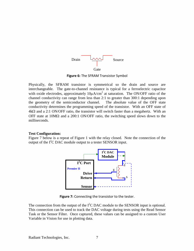
The symbol to be used to represent the SFRAM transistor in this application note is in
Figure 6.
Radiant Technologies, Inc. 7
Figure 6: The SFRAM Transistor Symbol
Physically, the SFRAM transistor is symmetrical so the drain and source are
interchangeable. The gate-to-channel resistance is typical for a ferroelectric capacitor
with oxide electrodes, approximately 10A/cm2 at saturation. The ON/OFF ratio of the
channel conductivity can range from less than 2:1 to greater than 300:1 depending upon
the geometry of the semiconductor channel. The absolute value of the OFF state
conductivity determines the programming speed of the transistor. With an OFF state of
4k and a 2:1 ON/OFF ratio, the transistor will switch faster than a megahertz. With an
OFF state at 10M and a 200:1 ON/OFF ratio, the switching speed slows down to the
milliseconds.
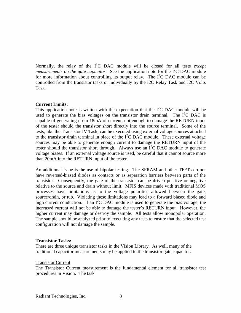
Test Configuration:
Figure 7 below is a repeat of Figure 1 with the relay closed. Note the connection of the
output of the I2C DAC module output to a tester SENSOR input.
Figure 7: Connecting the transistor to the tester.
The connection from the output of the I2C DAC module to the SENSOR input is optional.
This connection can be used to track the DAC voltage during tests using the Read Sensor
Task or the Sensor Filter. Once captured, these values can be assigned to a custom User
Variable in Vision for use in plotting data.
Premier II
Drive
Return
Sensor
I2C Port
I2C DAC
Module
s
d
g
Gate
Drain Source
Radiant Technologies, Inc. 8
Normally, the relay of the I2C DAC module will be closed for all tests except
measurements on the gate capacitor. See the application note for the I2C DAC module
for more information about controlling its output relay. The I2C DAC module can be
controlled from the transistor tasks or individually by the I2C Relay Task and I2C Volts
Task.
Current Limits:
This application note is written with the expectation that the I2C DAC module will be
used to generate the bias voltages on the transistor drain terminal. The I2C DAC is
capable of generating up to 18mA of current, not enough to damage the RETURN input
of the tester should the transistor short directly into the source terminal. Some of the
tests, like the Transistor IV Task, can be executed using external voltage sources attached
to the transistor drain terminal in place of the I2C DAC module. These external voltage
sources may be able to generate enough current to damage the RETURN input of the
tester should the transistor short through. Always use an I2C DAC module to generate
voltage biases. If an external voltage source is used, be careful that it cannot source more
than 20mA into the RETURN input of the tester.
An additional issue is the use of bipolar testing. The SFRAM and other TFFTs do not
have reversed-biased diodes as contacts or as separation barriers between parts of the
transistor. Consequently, the gate of the transistor can be driven positive or negative
relative to the source and drain without limit. MFIS devices made with traditional MOS
processes have limitations as to the voltage polarities allowed between the gate,
source/drain, or tub. Violating these limitations may lead to a forward biased diode and
high current conduction. If an I2C DAC module is used to generate the bias voltage, the
increased current will not be able to damage the tester’s RETURN input. However, the
higher current may damage or destroy the sample. All tests allow monopolar operation.
The sample should be analyzed prior to executing any tests to ensure that the selected test
configuration will not damage the sample.
Transistor Tasks:
There are three unique transistor tasks in the Vision Library. As well, many of the
traditional capacitor measurements may be applied to the transistor gate capacitor.
Transistor Current
The Transistor Current measurement is the fundamental element for all transistor test
procedures in Vision. The task

Radiant Technologies, Inc. 9
1) accepts fixed voltages for the drain and gate terminals of the transistor,
2) applies those voltages,
3) waits for the designated delay period,
4) measures the current through the channel, and
5) Plots the current vs time for the measurement period.
The last few points of the current measurement are averaged and used to calculate
equivalent resistance and resistivity values for the channel. Both the time evolution of
the current as well as the end point calculations of the measurement are saved in the
dataset database. The current vs time plot can be passed to the Collect-Plot Filter while
the end point values can be passed as single points to a Single-Point Filter.
Radiant Technologies, Inc. 10
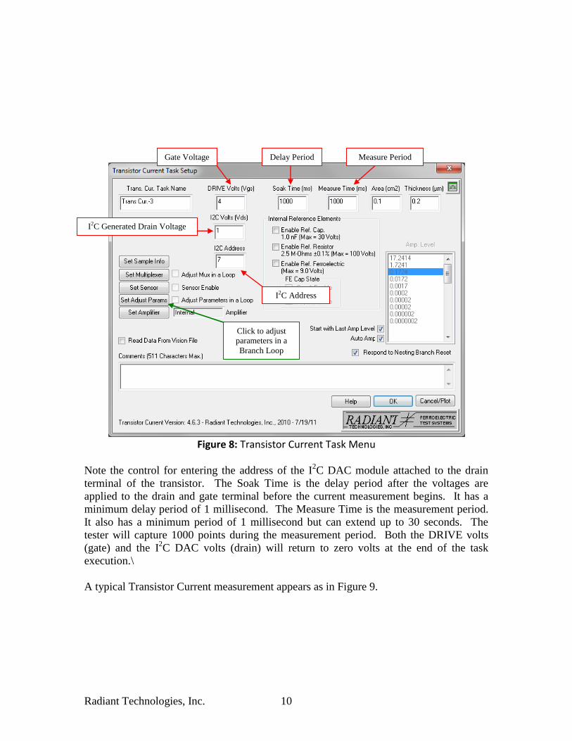
Figure 8: Transistor Current Task Menu
Note the control for entering the address of the I2C DAC module attached to the drain
terminal of the transistor. The Soak Time is the delay period after the voltages are
applied to the drain and gate terminal before the current measurement begins. It has a
minimum delay period of 1 millisecond. The Measure Time is the measurement period.
It also has a minimum period of 1 millisecond but can extend up to 30 seconds. The
tester will capture 1000 points during the measurement period. Both the DRIVE volts
(gate) and the I2C DAC volts (drain) will return to zero volts at the end of the task
execution.\
A typical Transistor Current measurement appears as in Figure 9.
Gate Voltage
I2C Generated Drain Voltage
I2C Address
Delay Period Measure Period
Click to adjust
parameters in a
Branch Loop
Radiant Technologies, Inc. 11
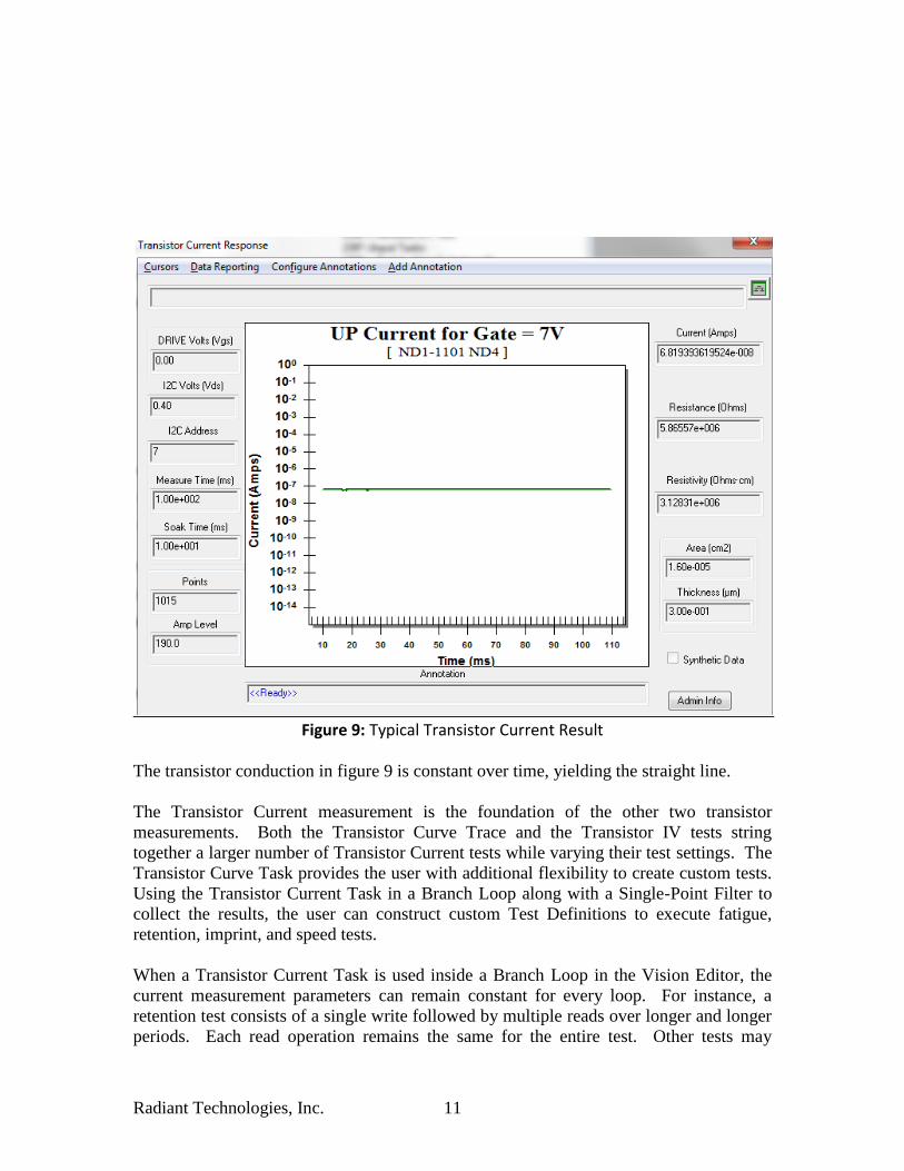
Figure 9: Typical Transistor Current Result
The transistor conduction in figure 9 is constant over time, yielding the straight line.
The Transistor Current measurement is the foundation of the other two transistor
measurements. Both the Transistor Curve Trace and the Transistor IV tests string
together a larger number of Transistor Current tests while varying their test settings. The
Transistor Curve Task provides the user with additional flexibility to create custom tests.
Using the Transistor Current Task in a Branch Loop along with a Single-Point Filter to
collect the results, the user can construct custom Test Definitions to execute fatigue,
retention, imprint, and speed tests.
When a Transistor Current Task is used inside a Branch Loop in the Vision Editor, the
current measurement parameters can remain constant for every loop. For instance, a
retention test consists of a single write followed by multiple reads over longer and longer
periods. Each read operation remains the same for the entire test. Other tests may
Radiant Technologies, Inc. 12
require the gate or drain parameters to change in each loop. For instance, the gate
voltage might increment on each loop. To accomplish this, click on the “Set Adjust
Parameters” button to open a new menu that lists the parameters that may be changed in a
loop and to establish how they change. This button is denoted in Figure 8 with the green
box and pointer.
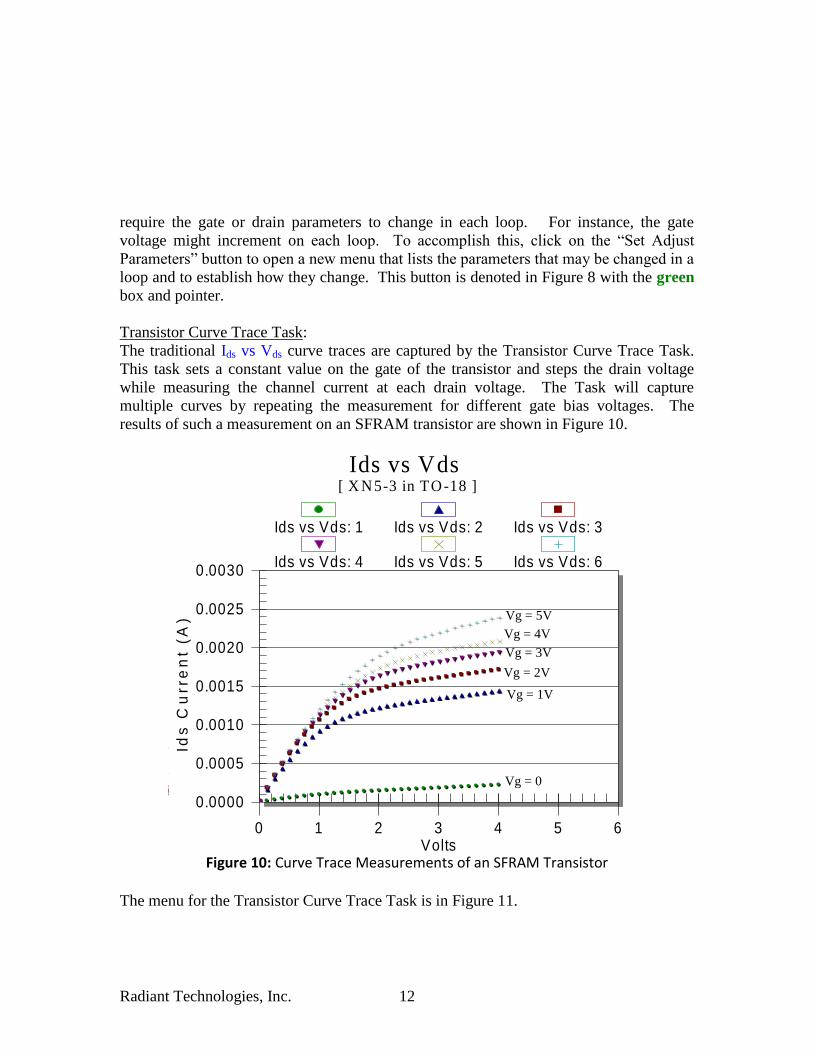
Transistor Curve Trace Task:
The traditional Ids vs Vds curve traces are captured by the Transistor Curve Trace Task.
This task sets a constant value on the gate of the transistor and steps the drain voltage
while measuring the channel current at each drain voltage. The Task will capture
multiple curves by repeating the measurement for different gate bias voltages. The
results of such a measurement on an SFRAM transistor are shown in Figure 10.
Figure 10: Curve Trace Measurements of an SFRAM Transistor
The menu for the Transistor Curve Trace Task is in Figure 11.
0.0000
0.0005
0.0010
0.0015
0.0020
0.0025
0.0030
0 1 2 3 4 5 6
Ids vs Vds [ X N 5-3 in TO -18 ]
Ids
Cu
rre
nt
(A)
Volts
Ids vs Vds: 1 Ids vs Vds: 2 Ids vs Vds: 3
Ids vs Vds: 4 Ids vs Vds: 5 Ids vs Vds: 6
Vg = 0
Vg = 1V
Vg = 2V
Vg = 3V
Vg = 4V
Vg = 5V
Radiant Technologies, Inc. 13
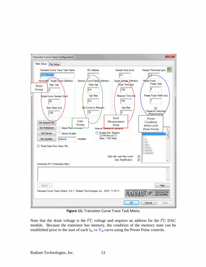
Figure 11: Transistor Curve Trace Task Menu
Note that the drain voltage is the I
2C voltage and requires an address for the I
2C DAC
module. Because the transistor has memory, the condition of the memory state can be
established prior to the start of each Ids vs Vds curve using the Preset Pulse controls.
Drain
Sweep
Gate
Sweep
Each
Measurement
Point
Preset
Condition
before each
Drain Sweep
Radiant Technologies, Inc. 14
Although the Transistor Curve Trace Task is designed for low current memory
transistors, it will measure traditional transistors. The MFP102 N-channel JFET
transistor, available at Radio Shack, conducts with no gate voltage but turns off as the
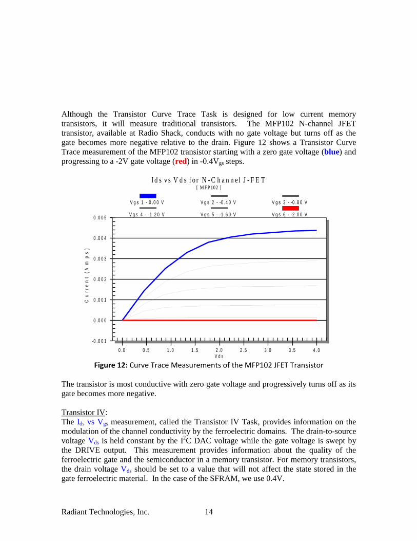
gate becomes more negative relative to the drain. Figure 12 shows a Transistor Curve
Trace measurement of the MFP102 transistor starting with a zero gate voltage (blue) and
progressing to a -2V gate voltage (red) in -0.4Vgs steps.
Figure 12: Curve Trace Measurements of the MFP102 JFET Transistor
The transistor is most conductive with zero gate voltage and progressively turns off as its
gate becomes more negative.
Transistor IV:
The Ids vs Vgs measurement, called the Transistor IV Task, provides information on the
modulation of the channel conductivity by the ferroelectric domains. The drain-to-source
voltage Vds is held constant by the I2C DAC voltage while the gate voltage is swept by
the DRIVE output. This measurement provides information about the quality of the
ferroelectric gate and the semiconductor in a memory transistor. For memory transistors,
the drain voltage Vds should be set to a value that will not affect the state stored in the
gate ferroelectric material. In the case of the SFRAM, we use 0.4V.
-0 .0 0 1
0 .0 0 0
0 .0 0 1
0 .0 0 2
0 .0 0 3
0 .0 0 4
0 .0 0 5
0 .0 0 .5 1 .0 1 .5 2 .0 2 .5 3 .0 3 .5 4 .0
I d s v s V d s f o r N - C h a n n el J - F E T[ M F P 102 ]
Cu
rr
en
t (
Am
ps
)
V d s
V g s 1 - 0 .0 0 V V g s 2 - -0 .4 0 V V g s 3 - -0 .8 0 V
V g s 4 - -1 .2 0 V V g s 5 - -1 .6 0 V V g s 6 - -2 .0 0 V
Radiant Technologies, Inc. 15
The default gate stimulus waveform is the same triangle wave used by Vision’s
Hysteresis Task. The comparison between the Hysteresis test and the Transistor IV test
is interesting. The Hysteresis Task drives a triangle wave directly into a capacitor and
measures the charge that comes out. The Transistor IV task drives the triangle wave into
the gate of a transistor and measures the current the transistor conducts! Both result in a
hysteresis loop.
Since the gate of the SFRAM transistor has memory, its initial state will affect the
response of the transistor to the measurement stimulus. The remanent polarization state
of the gate must be preset with a pulse prior to making a measurement. There are two
binary parameters of the test which simplify the response of the transistor.
1) The UP or DOWN saturated memory state of the gate ferroelectric before the test.
2) The initial polarity of the gate stimulus waveform.
This leads to four combinations of possible transistor responses:
1) Gate UP, Measure UP
2) Gate DOWN, Measure UP
3) Gate UP, Measure DOWN
4) Gate DOWN, Measure DOWN
The four possible test conditions may be combined into two test profiles:
Non-switching
Gate UP, Measure UP
Gate DOWN, Measure DOWN
or
Switching
Gate DOWN, Measure UP
Gate UP, Measure DOWN
The test profile below accomplishes the non-switching combination.
Radiant Technologies, Inc. 16
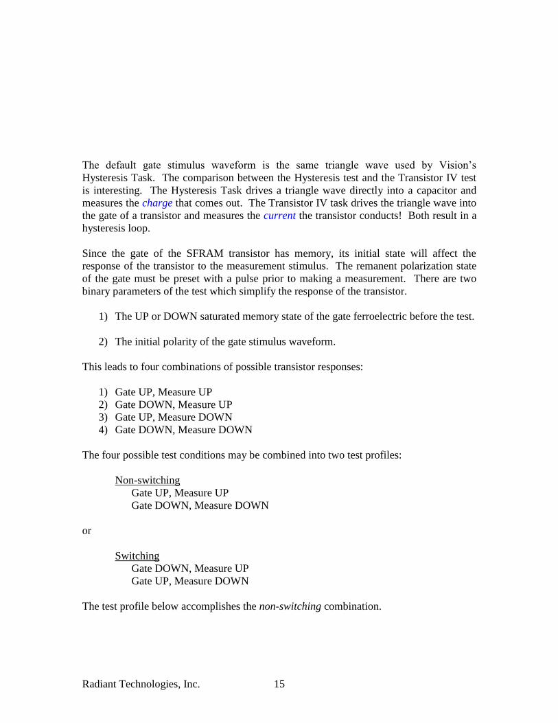
Figure 13: Non-switching Transistor Gate Stimulus Waveform
The preset pulse before each half of the triangle waveform isolates the second half of the
test from the first half of the test. This isolation can be eliminated by setting the present
pulse amplitude to zero volts. The non-switching Transistor IV test separates the
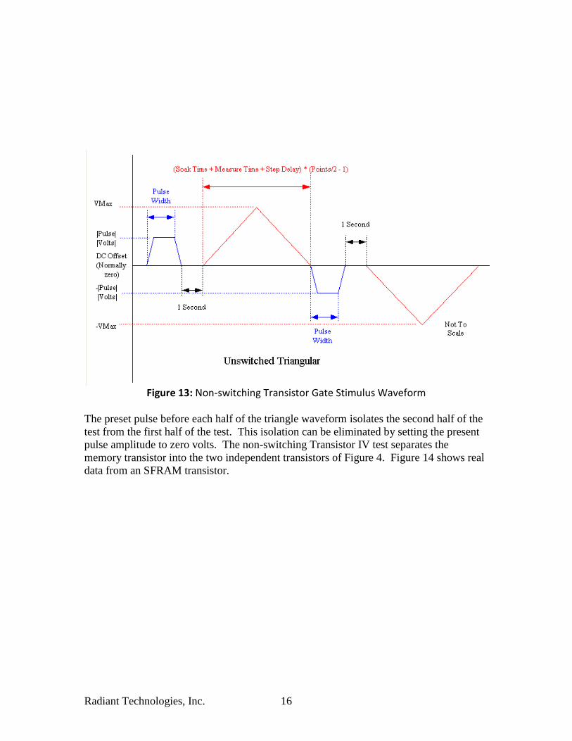
memory transistor into the two independent transistors of Figure 4. Figure 14 shows real
data from an SFRAM transistor.
Radiant Technologies, Inc. 17
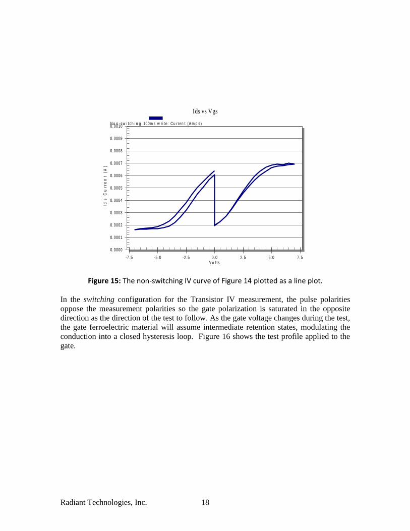
Figure 14: Non-switching Results for IV Measurement of an SFRAM
The preset pulses for the test in Figure 14 were set to saturate the transistor gate in either
direction. Consequently, no domains change orientation during each half of the
measurement so the conduction curves re-trace over themselves. The slight open nature
of the two loops arises from the same mechanism as the “gap” in the polarization loop.
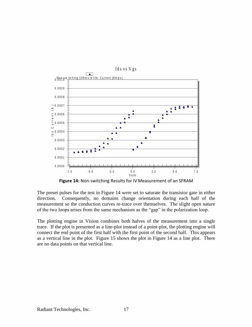
The plotting engine in Vision combines both halves of the measurement into a single
trace. If the plot is presented as a line-plot instead of a point-plot, the plotting engine will
connect the end point of the first half with the first point of the second half. This appears
as a vertical line in the plot. Figure 15 shows the plot in Figure 14 as a line plot. There
are no data points on that vertical line.
0 .0 0 0 0
0 .0 0 0 1
0 .0 0 0 2
0 .0 0 0 3
0 .0 0 0 4
0 .0 0 0 5
0 .0 0 0 6
0 .0 0 0 7
0 .0 0 0 8
0 .0 0 0 9
0 .0 0 1 0
-7 .5 -5 .0 -2 .5 0 .0 2 .5 5 .0 7 .5
I d s v s V g s
Ids
Cu
rr
en
t (
A)
V o l ts
N o n -s w i tc h i n g 1 0 0 m s w r i te : C u r r e n t (A m p s )
Radiant Technologies, Inc. 18
Figure 15: The non-switching IV curve of Figure 14 plotted as a line plot.
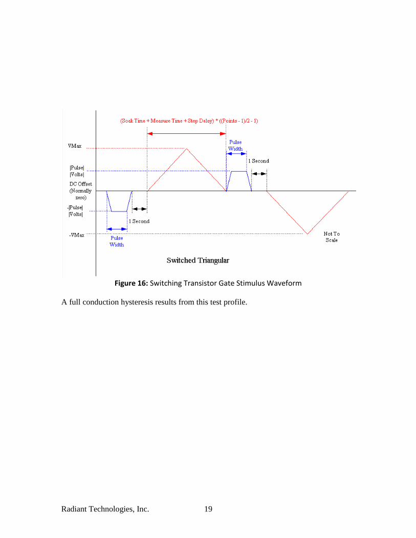
In the switching configuration for the Transistor IV measurement, the pulse polarities
oppose the measurement polarities so the gate polarization is saturated in the opposite
direction as the direction of the test to follow. As the gate voltage changes during the test,
the gate ferroelectric material will assume intermediate retention states, modulating the
conduction into a closed hysteresis loop. Figure 16 shows the test profile applied to the
gate.
0. 0000
0. 0001
0. 0002
0. 0003
0. 0004
0. 0005
0. 0006
0. 0007
0. 0008
0. 0009
0. 0010
-7. 5 -5. 0 -2. 5 0. 0 2. 5 5. 0 7. 5
Ids vs Vgs Id
s C
urr
en
t (A
)
V o l t s
N o n -s w i t c h i n g 100m s w r i t e: C u rren t (A m p s )
Radiant Technologies, Inc. 19
Figure 16: Switching Transistor Gate Stimulus Waveform
A full conduction hysteresis results from this test profile.
Radiant Technologies, Inc. 20
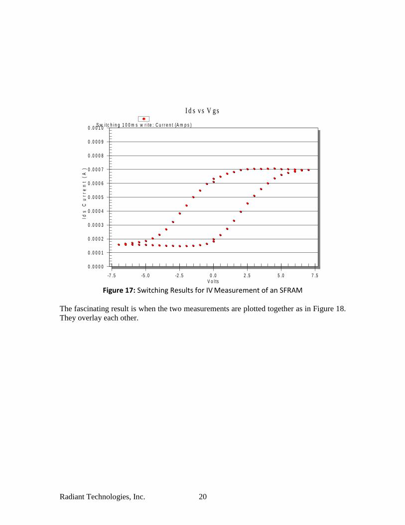
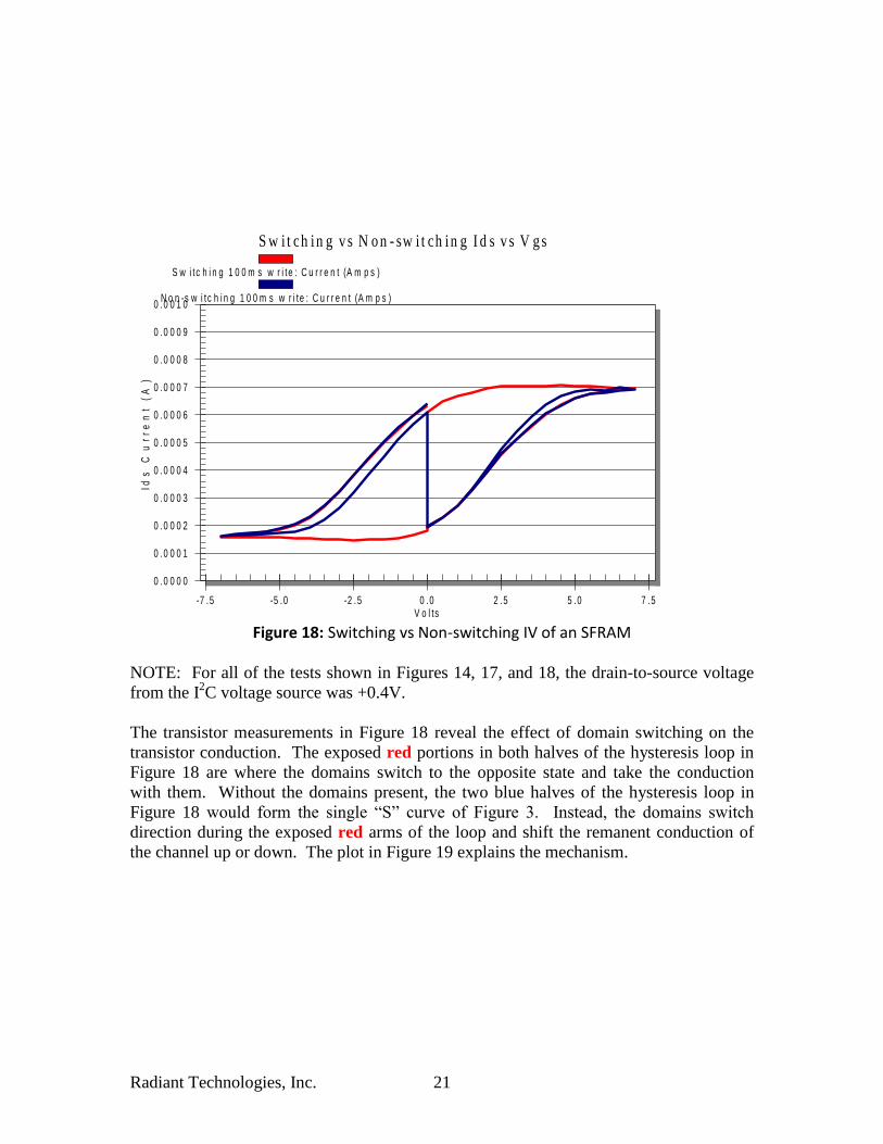
Figure 17: Switching Results for IV Measurement of an SFRAM
The fascinating result is when the two measurements are plotted together as in Figure 18.
They overlay each other.
0 .0 0 0 0
0 .0 0 0 1
0 .0 0 0 2
0 .0 0 0 3
0 .0 0 0 4
0 .0 0 0 5
0 .0 0 0 6
0 .0 0 0 7
0 .0 0 0 8
0 .0 0 0 9
0 .0 0 1 0
-7 .5 -5 .0 -2 .5 0 .0 2 .5 5 .0 7 .5
I d s v s V g s
Ids
Cu
rr
en
t (
A)
V o l ts
S w i tc h i n g 1 0 0 m s w r i te : C u r r e n t (A m p s )
Radiant Technologies, Inc. 21
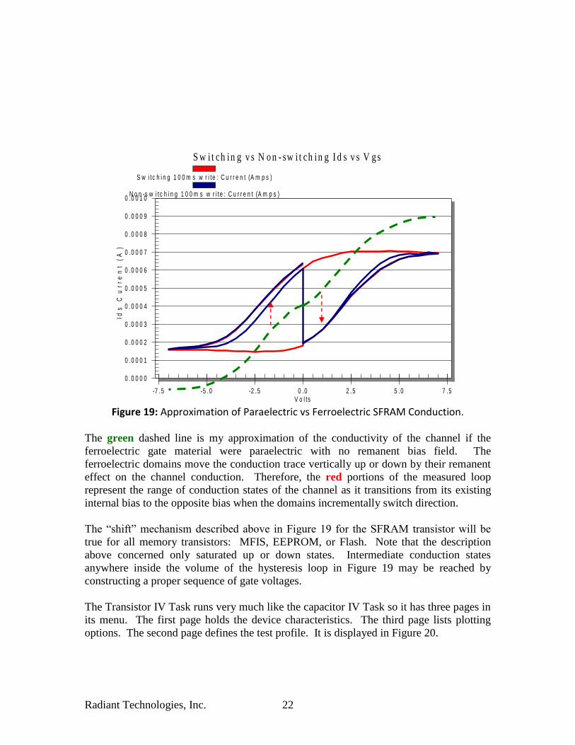
Figure 18: Switching vs Non-switching IV of an SFRAM
NOTE: For all of the tests shown in Figures 14, 17, and 18, the drain-to-source voltage
from the I2C voltage source was +0.4V.
The transistor measurements in Figure 18 reveal the effect of domain switching on the
transistor conduction. The exposed red portions in both halves of the hysteresis loop in
Figure 18 are where the domains switch to the opposite state and take the conduction
with them. Without the domains present, the two blue halves of the hysteresis loop in
Figure 18 would form the single “S” curve of Figure 3. Instead, the domains switch
direction during the exposed red arms of the loop and shift the remanent conduction of
the channel up or down. The plot in Figure 19 explains the mechanism.
0 .0 0 0 0
0 .0 0 0 1
0 .0 0 0 2
0 .0 0 0 3
0 .0 0 0 4
0 .0 0 0 5
0 .0 0 0 6
0 .0 0 0 7
0 .0 0 0 8
0 .0 0 0 9
0 .0 0 1 0
-7 .5 -5 .0 -2 .5 0 .0 2 .5 5 .0 7 .5
S w i t ch in g v s N o n - sw i t ch in g I d s v s V g s
Ids
Cu
rr
en
t (
A)
V o l ts
S w i tc h i n g 1 0 0 m s w r i te : C u r r e n t (A m p s )
N o n -s w i tc h i n g 1 0 0 m s w r i te : C u r r e n t (A m p s )
Radiant Technologies, Inc. 22
Figure 19: Approximation of Paraelectric vs Ferroelectric SFRAM Conduction.
The green dashed line is my approximation of the conductivity of the channel if the
ferroelectric gate material were paraelectric with no remanent bias field. The
ferroelectric domains move the conduction trace vertically up or down by their remanent
effect on the channel conduction. Therefore, the red portions of the measured loop
represent the range of conduction states of the channel as it transitions from its existing
internal bias to the opposite bias when the domains incrementally switch direction.
The “shift” mechanism described above in Figure 19 for the SFRAM transistor will be
true for all memory transistors: MFIS, EEPROM, or Flash. Note that the description
above concerned only saturated up or down states. Intermediate conduction states
anywhere inside the volume of the hysteresis loop in Figure 19 may be reached by
constructing a proper sequence of gate voltages.
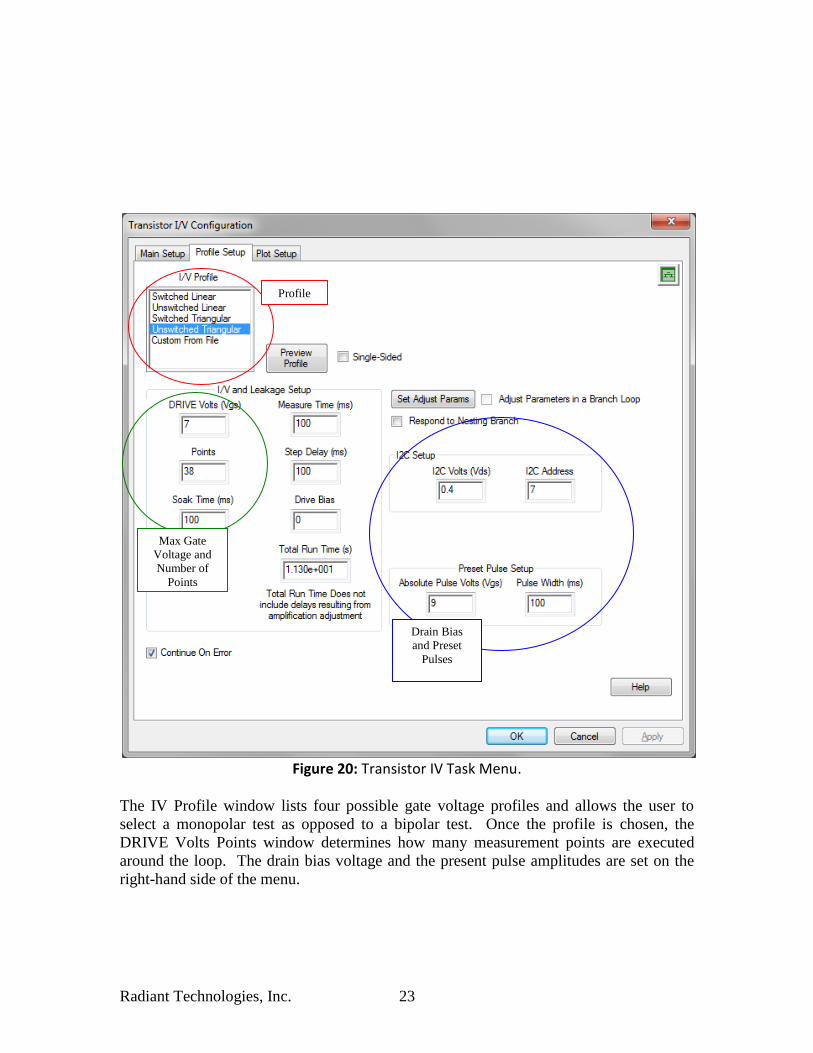
The Transistor IV Task runs very much like the capacitor IV Task so it has three pages in
its menu. The first page holds the device characteristics. The third page lists plotting
options. The second page defines the test profile. It is displayed in Figure 20.
0 .0 0 0 0
0 .0 0 0 1
0 .0 0 0 2
0 .0 0 0 3
0 .0 0 0 4
0 .0 0 0 5
0 .0 0 0 6
0 .0 0 0 7
0 .0 0 0 8
0 .0 0 0 9
0 .0 0 1 0
-7 .5 -5 .0 -2 .5 0 .0 2 .5 5 .0 7 .5
S w i t ch in g v s N o n - sw i t ch in g I d s v s V g s
Ids
Cu
rr
en
t (
A)
V o l ts
S w i tc h i n g 1 0 0 m s w r i te : C u r r e n t (A m p s )
N o n -s w i tc h i n g 1 0 0 m s w r i te : C u r r e n t (A m p s )
Radiant Technologies, Inc. 23
Figure 20: Transistor IV Task Menu.
The IV Profile window lists four possible gate voltage profiles and allows the user to
select a monopolar test as opposed to a bipolar test. Once the profile is chosen, the
DRIVE Volts Points window determines how many measurement points are executed
around the loop. The drain bias voltage and the present pulse amplitudes are set on the
right-hand side of the menu.
Profile
Max Gate
Voltage and
Number of
Points
Drain Bias
and Preset
Pulses
Radiant Technologies, Inc. 24
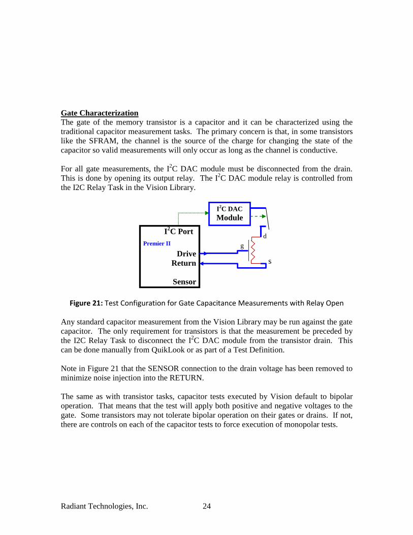
Gate Characterization
The gate of the memory transistor is a capacitor and it can be characterized using the
traditional capacitor measurement tasks. The primary concern is that, in some transistors
like the SFRAM, the channel is the source of the charge for changing the state of the
capacitor so valid measurements will only occur as long as the channel is conductive.
For all gate measurements, the I2C DAC module must be disconnected from the drain.
This is done by opening its output relay. The I2C DAC module relay is controlled from
the I2C Relay Task in the Vision Library.
Figure 21: Test Configuration for Gate Capacitance Measurements with Relay Open
Any standard capacitor measurement from the Vision Library may be run against the gate
capacitor. The only requirement for transistors is that the measurement be preceded by
the I2C Relay Task to disconnect the I2C DAC module from the transistor drain. This
can be done manually from QuikLook or as part of a Test Definition.
Note in Figure 21 that the SENSOR connection to the drain voltage has been removed to
minimize noise injection into the RETURN.
The same as with transistor tasks, capacitor tests executed by Vision default to bipolar
operation. That means that the test will apply both positive and negative voltages to the
gate. Some transistors may not tolerate bipolar operation on their gates or drains. If not,
there are controls on each of the capacitor tests to force execution of monopolar tests.
Premier II
Drive
Return
Sensor
I2C Port
I2C DAC
Module
s
d
g
Radiant Technologies, Inc. 25
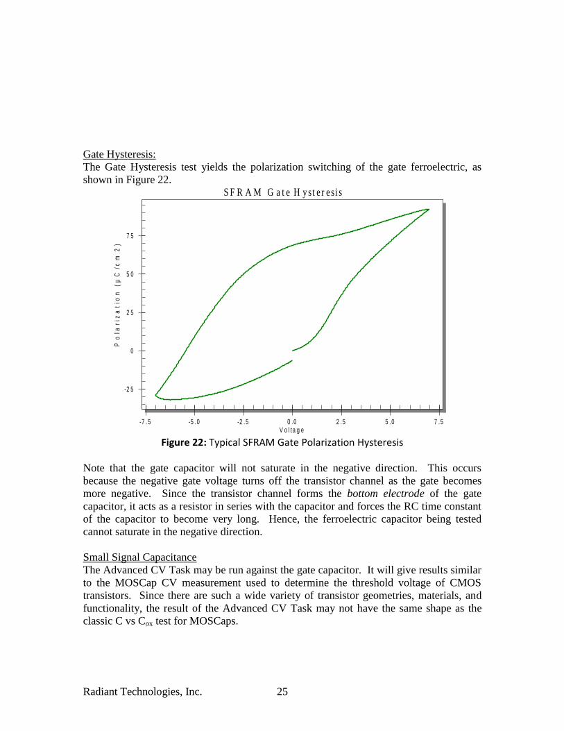
Gate Hysteresis:
The Gate Hysteresis test yields the polarization switching of the gate ferroelectric, as
shown in Figure 22.
Figure 22: Typical SFRAM Gate Polarization Hysteresis
Note that the gate capacitor will not saturate in the negative direction. This occurs
because the negative gate voltage turns off the transistor channel as the gate becomes
more negative. Since the transistor channel forms the bottom electrode of the gate
capacitor, it acts as a resistor in series with the capacitor and forces the RC time constant
of the capacitor to become very long. Hence, the ferroelectric capacitor being tested
cannot saturate in the negative direction.
Small Signal Capacitance
The Advanced CV Task may be run against the gate capacitor. It will give results similar
to the MOSCap CV measurement used to determine the threshold voltage of CMOS
transistors. Since there are such a wide variety of transistor geometries, materials, and
functionality, the result of the Advanced CV Task may not have the same shape as the
classic C vs Cox test for MOSCaps.
-2 5
0
2 5
5 0
7 5
-7 .5 -5 .0 -2 .5 0 .0 2 .5 5 .0 7 .5
S F R A M G a t e H y st e r esi s
Po
lar
iza
tio
n (
µC
/cm
2)
V o l ta g e
Radiant Technologies, Inc. 26
Leakage
Once the I2DAC module has been disconnected from the transistor drain connection, the
Vision Leakage Task may be run on the gate capacitor. This task measures current like
the Transistor Current task but it is executed in a different manner only possible with
capacitors. It has two orders of magnitude more resolution than does the Transistor
Current task. Remember to account for the effect of channel conduction modulation by
the gate voltage when analyzing the results.
Long Term Reliability Long term reliability is a most important factor when testing memory transistors.
Fatigue, retention, and imprint may be evaluated by building custom Test Definitions in
the Vision Editor using the Transistor Current Task.
Retention:
Retention is tested simply by writing the gate once in the desired direction and then non-
destructively measuring over time the current conduction of the device with Vgs = 0V and
a non-disturbing value for Vds. The results for such a retention test of a recently
fabricated SFRAM device are shown below.
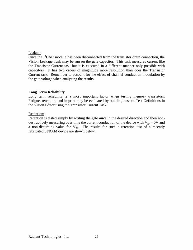
Radiant Technologies, Inc. 27
Figure 23: Retention at Room Temperature Over Night.
(Vwr = ±7V, 100ms)
Note that X-axis scale in Figure 23 is in units of Log(seconds). On this plot, 1x10⁹
seconds is equal to 30 years retention time. The plot shows ten years retention at room
temperature for this TFFT.
The retention test is constructed with the following test loop:
I2C Volts = 0, Relay closed
Simple Pulse Program the transistor up or down
Delay Increase the retention time by x3 each loop using the Set
Parameters button
Transistor Current Read the transistor retained current state
Single Point Filter Plot the transistor current measurement vs Delay time.
Branch Loop Loop until the retention period is complete.
Repeat the retention test again in the opposite state.
Collect/Plot Plot the up and down retention results against each other.
0.00000
0.00025
0.00050
0.00075
0.00100
0.00125
0.00150
100 101 102 103 104 105 106 107 108
P O S a n d N E G 7 V R e te n t io n R o o m T e m p D a rk[ N D 1-0903 W 4 N D 7 ]
Ids
Cu
rr
en
t (
A)
Retention (s )
Plot PO S Retention: Single-Point F ilter: 1
Plot N EG Retention: Single-Point F ilter: 1
Radiant Technologies, Inc. 28
Note that the Vision Library has a scheduling task which will set the specified time and
date to begin execution of the test definition. I use this task to delay execution of
retention tests until late in the evening when the laboratory is empty and there will be no
disturbances to interfere with the accuracy of the test.
Fatigue:
A transistor fatigue test has roughly the same format as the retention test with the
exception that the Delay Task is replaced with the Waveform Task to cycle the gate
between measurement points. I suggest measuring both the up and down states after each
cycling period.
I2C Volts = 0v, Relay closed
Waveform Increase the cycle time by x3 each loop using the Set
Parameters button
Simple Pulse UP Program the transistor UP
Transistor Current Read the transistor UP current state
Simple Pulse DOWN Program the transistor DOWN
Transistor Current Read the transistor UP current state
Single Point Filter Plot the UP/DOWN Conduction vs Cumulative Cycles
Branch Loop Loop until the fatigue limit is reached.
Imprint:
Imprint tests measure retention vs cumulative time as a function one of three conditions:
1) no stimulus, 2) temperature, or 3) single-sided pulses. The imprint of a memory
transistor may be tested in three ways. The first is to examine the slope, if any, of the up
or down signal from a retention test. Any “retention loss” may result from imprint but
also could result from thermodynamic de-poling of the domains. The second method is
to execute the Transistor IV Task multiple times as a function of imprint time to identify
shifts in the conduction curves left or right. The third is to run a traditional capacitor
imprint task on the gate capacitor alone. One possible IV imprint test loop is outline
below.
Transistor IV Initial IV state
Delay Increase x 3 in each loop using the Set Parameters button
Transistor IV Measure the transistor channel conduction hysteresis
Collect Plot Plot the IV loop. Set the task to append each test within the
Branch Loop.
Branch Loop Loop until the imprint period is complete.
Radiant Technologies, Inc. 29
The result will be a series of channel IV loops. With no imprint, the loops should
overlay. With imprint, the loops will drift in one direction, usually as a function of
Log(time).
Speed Tests An important aspect of memory transistors is how long it takes to write their new state.
This characteristic may be tested in a Branch Loop using the Transistor Current Task.
Simple Pulse program the transistor saturated in one direction
Transistor Current Measure the saturated state current conduction
Simple Pulse Program the transistor in the opposite direction with a fast
pulse, increasing the pulse width in each loop.
Transistor Current Read the transistor new current state
Single Point Filter Plot the transistor current measurements vs Delay time.
Branch Loop Loop until a saturating pulse is achieved.
Some transistors, like the SFRAM, may be asymmetrical in their programming speed.
Therefore, the speed test should be run twice, once in each direction.
Conclusion:
The Premier II and Multiferroic testers combined with Radiant’s new I2C DAC module
make it possible to use automated tests on nonvolatile transistors to fully characterize
their transistor, gate capacitor, and reliability properties.