test points and scan introduction to structured built-in ...test generation is performed by atpg; a...
TRANSCRIPT

Introduction to structured VLSI design
Design for Test (DfT) - Part 2Erik Larsson
EIT, Lund University
Outline
Test points and Scan Built-In Self-Test (BIST) Systems-on-chip test Boundary scan (IEEE 1149.1)
Integrated Circuits (IC)
Viper 2.0 RevB Analog/Digital TV Processor 10mm x 10 mm (100 mm2) ~10 M gates ~50 M transistors ~100 clock domains
Die
AND-gate
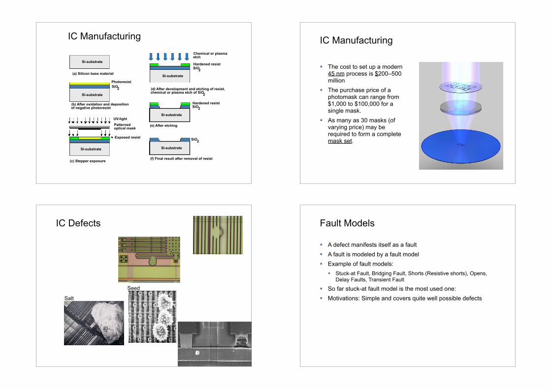
IC Manufacturing
Si-substrate
Si-substrate Si-substrate
(a) Silicon base material
(b) After oxidation and depositionof negative photoresist
(c) Stepper exposure
PhotoresistSiO2
UV-lightPatternedoptical mask
Exposed resist
SiO2
Si-substrate
Si-substrate
Si-substrate
SiO2
SiO2
(d) After development and etching of resist,chemical or plasma etch of SiO2
(e) After etching
(f) Final result after removal of resist
Hardened resist
Hardened resist
Chemical or plasmaetch
IC Manufacturing
The cost to set up a modern 45 nm process is $200–500 million
The purchase price of a photomask can range from $1,000 to $100,000 for a single mask.
As many as 30 masks (of varying price) may be required to form a complete mask set.
IC Defects
Salt
Seed
Fault Models
A defect manifests itself as a fault A fault is modeled by a fault model Example of fault models:
Stuck-at Fault, Bridging Fault, Shorts (Resistive shorts), Opens, Delay Faults, Transient Fault
So far stuck-at fault model is the most used one: Motivations: Simple and covers quite well possible defects
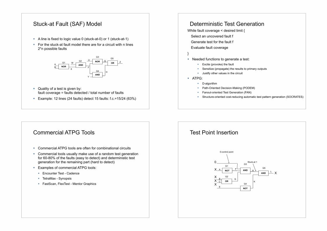
Stuck-at Fault (SAF) Model
A line is fixed to logic value 0 (stuck-at-0) or 1 (stuck-at-1) For the stuck-at fault model there are for a circuit with n lines
2*n possible faults
Quality of a test is given by: fault coverage = faults detected / total number of faults
Example: 12 lines (24 faults) detect 15 faults: f.c.=15/24 (63%)
ORNOR
AZ
BAND
NOR
AND
UW
X
Y
F
H
GG1
G2
G3
G4
G5
Deterministic Test GenerationWhile fault coverage < desired limit {
Select an uncovered fault fGenerate test for the fault fEvaluate fault coverage
} Needed functions to generate a test:
Excite (provoke) the fault Sensitize (propagate) the results to primary outputs Justify other values in the circuit
ATPG: D-algorithm Path-Oriented Decision-Making (PODEM) Fanout-oriented Test Generation (FAN) Structure-oriented cost-reducing automatic test pattern generation (SOCRATES)
Commercial ATPG Tools
Commercial ATPG tools are often for combinational circuits Commercial tools usually make use of a random test generation
for 60-80% of the faults (easy to detect) and deterministic test generation for the remaining part (hard to detect)
Examples of commercial ATPG tools: Encounter Test - Cadence TetraMax - Synopsis
FastScan, FlexTest - Mentor Graphics
Test Point Insertion
ANDA
L
B
NOT
OR
NOTE
F
C K
H
G1
G2
G4
G5
G
0-control point
AND
G3Stuck-at 10
X
XXX
X

Test Point Insertion
0-controllability 1-controllability
Original Observation
OP
CPCP
1/0-controllability
CP1
MUX
0
1
CP2
Combinational logic
Combinational logic
Sequential -> Combinational
Problem: ATPG works for combinational logic while most ICs are sequential
Solution: Provide a test mode in which flip flops can be accessed directly
Register provide virtual primary inputs/primary outputs
PI PO
Flip flops
1. Write flip flops2. Stimulus at inputs3. Normal cycle
launch/capture4. Observe output5. Read flip flops
PI PO
Flip flops
Combinational logic
Combinational logic
Scan Design Concept
Replace flip flop (FF) with scan flip flop (SFF): extra multiplexer on data input
Connect SFFs to form one or more scan chains Connect multiplexer control signal to scan enable
FFMUX
CLK
SE
Q
SO
DSI
FF
CLKQ
D
SFF
SE: Scan enableSI: Scan inputSO: Scan output
Sequential -> Combinational
Circuit can be in two modes: Functional mode and Test mode In Test mode test data can be shifted in and shifted out Test mode adds virtual PI and PO such that test data can be
directly applied to combinational logic ATPG for combinational logic works also for sequential
1. Write flip flops2. Stimulus at inputs3. Normal cycle
launch/capture4. Observe output5. Read flip flops
Combinational logic
Combinational logic
PI PO
Flip flops
PI PO
Flip flops
Combinational logic
Combinational logic

Scan Test Application - first attempt
Scan chain 1 (6 FFs)
SE
SI SO
A[0:4] Z[0:2]
Combinational logic
SE: 1 1 1 1 1 1 0 1 1 1 1 1 1 1 1 1 1 1 1 0 1 1 1 1 1 1 1 1 1 1 1 1 0 1 1 1 1 1 1 SI:
A[0:4]
stimulus response stimulus response stimulus response
Shift-in Shift-in Shift-in Shift-outShift-outShift-out
Capture Capture Capture
Test time=number of patterns *(shift-in + capture + shift-out)=3*(6+1+6)=39
Scan Test Application - second attempt
Scan chain 1 (6 FFs)
SE
SI SO
A[0:4] Z[0:2]
Combinational logic
SE: 1 1 1 1 1 1 0 1 1 1 1 1 1 0 1 1 1 1 1 1 0 1 1 1 1 1 1 SI:
A[0:4]
stimulus resp/stim res/stim response
Shift-in Shift-in/out Shift-outShift-in/outCapture Capture Capture
Test time=number of patterns *(shift-in + capture) + shift-out=3*(6+1)+6=27
Scan Benefits and Costs
Scan Benefits Automatic scan insertion
ATPG High fault coverage
Short test development time
EDA tools For scan insertion (converting
flip flops to scan flip flops)
Connection Partial scan selection
Scan stiching
Scan Costs Silicon area - Mux, scan
chain, scan enable Performance reduction -
Multiplexer in time-critical path IC pins - Scan-in (SI), scan-
out (SO), scan_enable (SE)
Test time - Serial shifting is slow
Delay Test
Stuck-at-fault test consist of one vector. Each vector applied at slow speed (DC-scan).
Timing related faults need two vectors and they are to be applied on consecutive clock cycles (at normal clock speed) (AC-scan)
At speed test: Vector V1 is applied to set the circuit in its state Vector V2 is applied
Response is captured
Three approaches: Launch-on-capture
Launch-on-shift Enhanced scan
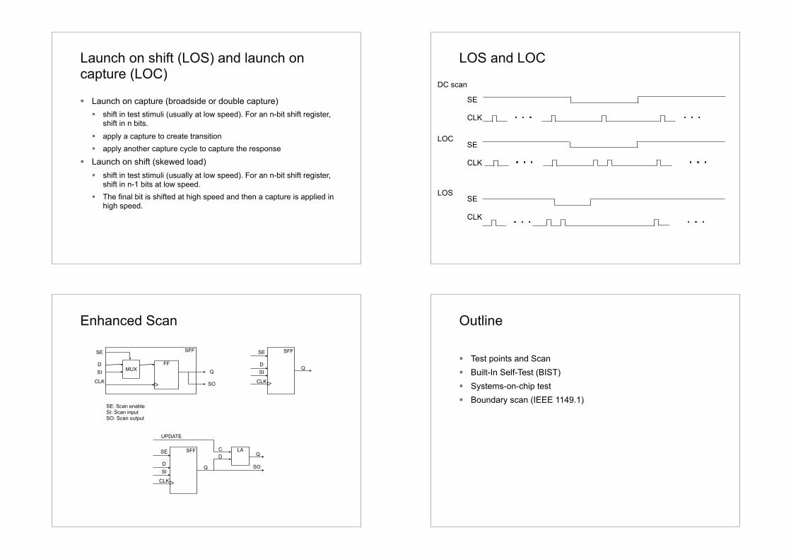
Launch on shift (LOS) and launch on capture (LOC)
Launch on capture (broadside or double capture) shift in test stimuli (usually at low speed). For an n-bit shift register,
shift in n bits.
apply a capture to create transition apply another capture cycle to capture the response
Launch on shift (skewed load) shift in test stimuli (usually at low speed). For an n-bit shift register,
shift in n-1 bits at low speed. The final bit is shifted at high speed and then a capture is applied in
high speed.
LOS and LOC
DC scan
LOC
LOS
SE
CLK
SE
CLK
SE
CLK
Enhanced Scan
FFMUX
CLK
SE
Q
SO
DSI
SFF
SE: Scan enableSI: Scan inputSO: Scan output
CLK
SE
QDSI
SFF
CLK
SE
QDSI
SFF LAQ
CD
SO
UPDATE
Outline
Test points and Scan Built-In Self-Test (BIST) Systems-on-chip test Boundary scan (IEEE 1149.1)

Built-In Self-Test
Key component to discuss: Test pattern storage/generation
Test stimuli storage/generation Test response analysis
Test control
In a non-BIST environment: test generation is performed by ATPG; a tool such as FastScan can
generate deterministic test patterns,
test stimuli and expected test responses are stored in the ATE, and the ATE controls the testing and performs test evaluation.
On-chip/off-chip
Device under test (DUT)Test source
Test sink
ATE
Off-chip
Device under test (DUT)Test source
Test sinkOn-chip
Test Pattern Generation
How store/generate test patterns on-chip?
Deterministic test patterns Exhaustive test patterns Pseudo-exhaustive/random test patterns Random test patterns
Commercial tools usually make use of a random test generation for 60-80% of the faults (easy to detect) and deterministic test generation for the remaining part (hard to detect)
Test Pattern Generation
Exhaustive test generation; simple hardware (a counter), 100% fault coverage but too time consuming
Deterministic test generation; high fault coverage but requires ATE for test pattern storage
Pseudo-exhaustive test generation using Linear-Feedback Shift-Registers (LFSR)
+
FF FF FF FF
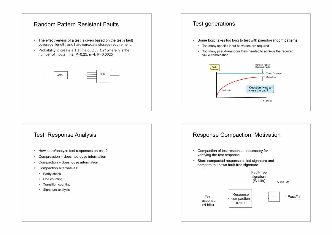
Random Pattern Resistant Faults
The effectiveness of a test is given based on the test’s fault coverage, length, and hardware/data storage requirement.
Probability to create a 1 at the output; 1/2n where n is the number of inputs. n=2; P=0.25, n=4; P=0.0625
AND AND
Test generations
Some logic takes too long to test with pseudo-random patterns Too many specific input bit values are required
Too many pseudo-random trials needed to achieve the required value combination
Test Response Analysis
How store/analyze test responses on-chip? Compression – does not loose information Compaction – does loose information Compaction alternatives:
Parity check One counting
Transition counting Signature analysis
Response Compaction: Motivation
Compaction of test responses necessary for verifying the test response
Store compacted response called signature and compare to known fault-free signature
Responsecompaction
circuit=Test
response(N bits)
Fault-freesignature(W bits)
Pass/fail
N >> W
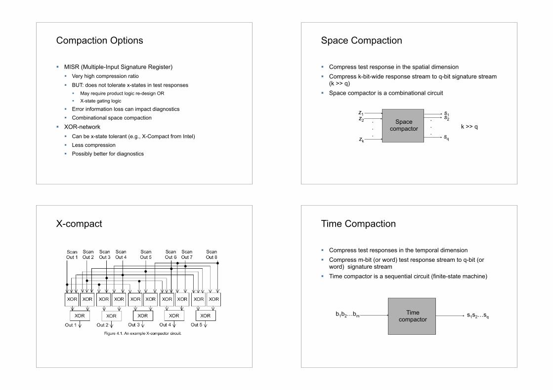
Compaction Options
MISR (Multiple-Input Signature Register) Very high compression ratio
BUT: does not tolerate x-states in test responses May require product logic re-design OR X-state gating logic
Error information loss can impact diagnostics Combinational space compaction
XOR-network Can be x-state tolerant (e.g., X-Compact from Intel) Less compression Possibly better for diagnostics
Space Compaction
Compress test response in the spatial dimension Compress k-bit-wide response stream to q-bit signature stream
(k >> q) Space compactor is a combinational circuit
.
.
.
z1z2
zk
s1...
s2
sq
Spacecompactor k >> q
X-compact Time Compaction
Compress test responses in the temporal dimension Compress m-bit (or word) test response stream to q-bit (or
word) signature stream Time compactor is a sequential circuit (finite-state machine)
Timecompactor
b1b2…bm s1s2…sq
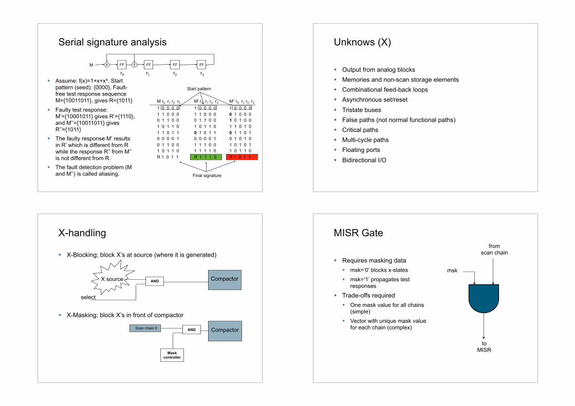
Serial signature analysis
Assume: f(x)=1+x+x4, Start pattern (seed): {0000}, Fault-free test response sequence M={10011011}, gives R={1011}
Faulty test response: M’={10001011} gives R’={1110}, and M’’={10011011} gives R’’={1011}
The faulty response M’ results in R’ which is different from R while the response R’’ from M’’ is not different from R.
The fault detection problem (M and M’’) is called aliasing.
M r0 r1 r2 r3
1 0 0 0 01 1 0 0 00 1 1 0 01 0 1 1 01 1 0 1 10 0 0 0 10 1 1 0 01 0 1 1 0R 1 0 1 1
M’ r0 r1 r2 r3
1 0 0 0 01 1 0 0 00 1 1 0 01 0 1 1 00 1 0 1 10 0 0 0 11 1 1 0 01 1 1 1 0R’ 1 1 1 0
M’’ r0 r1 r2 r3
1 0 0 0 00 1 0 0 01 0 1 0 01 1 0 1 00 1 1 0 10 1 0 1 01 0 1 0 11 0 1 1 0R 1 0 1 1
Start pattern
Final signature
FFFFFFFF
+ +
M
r0 r1 r2 r3
Unknows (X)
Output from analog blocks Memories and non-scan storage elements Combinational feed-back loops Asynchronous set/reset Tristate buses False paths (not normal functional paths) Critical paths Multi-cycle paths Floating ports Bidirectional I/O
X-handling
X-Blocking; block X’s at source (where it is generated)
X-Masking; block X’s in front of compactor
CompactorX source AND
select
AND Compactor Scan chain 0
Mask controller
MISR Gate
Requires masking data msk=‘0’ blocks x-states
msk=‘1’ propagates test responses
Trade-offs required One mask value for all chains
(simple)
Vector with unique mask value for each chain (complex)
from scan chain
toMISR
msk
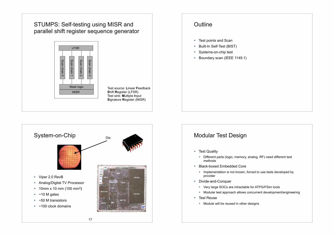
STUMPS: Self-testing using MISR and parallel shift register sequence generator
Test source: Linear Feedback Shift Register (LFSR)Test sink: Multiple Input Signature Register (MISR)
Scan chain 1
Scan chain 0
Scan chain 2
Scan chain 3
Mask logic
LFSR
MISR
Outline
Test points and Scan Built-In Self-Test (BIST) Systems-on-chip test Boundary scan (IEEE 1149.1)
17
System-on-Chip
Viper 2.0 RevB Analog/Digital TV Processor 10mm x 10 mm (100 mm2) ~10 M gates ~50 M transistors ~100 clock domains
Die Modular Test Design
Test Quality Different parts (logic, memory, analog, RF) need different test
methods
Black-boxed Embedded Core Implementation is not known, forced to use tests developed by
provider
Divide-and-Conquer Very large SOCs are intractable for ATPG/FSim tools Modular test approach allows concurrent development/engineering
Test Reuse Module will be reused in other designs

Challenges
Distributed Design and Test Development Standardized set of deliverables
Test Access to Embedded Modules Standardized on-chip test access hardware Tools for test translation
Chip-Level Test Optimization Tools to evaluate trade-offs; minimal impact on design (extra
silicon, delay) at minimizing test application time and ATE memory requirement
Generic Test Access Architecture
Test pattern Source and Sink Store/generate test stimuli and store/evaluate test responses
Test Access Mechanism (TAM) Transports test patterns to/from module under test (MUT)
Test Wrapper Provides test access to MUT Isolates MUT at test
CPU
wrapper
MUT
SRAMUDL
DSP DRAM
ROMPCI
source
sink
TAMTAM
Test Planning
Objectives: Optimizing test access to cores and scheduling test hardware
Core import
Core integration
Test wrapper& TAM design
Test hardware planningCore test import
Test assembly
Test scheduling
Top-level ATPG•Glue logic, soft cores•Test wrappers
Test software planning
IEEE 1500 Core Test Standard
Goals Define test interface between core and SOC
Core isolation Plug-and-play protocols
Scope Standardize core isolation protocols and test modes TAM design
Type of test to be applied Test scheduling

IEEE 1500 Wrapper
wrapper
Core
WBY
WIR
WBR
WBR
WBR
WBR
Test control+test stimuli
Test stimuli
Functional data
Test responses
Functional data
Test control+test responses
WIP
Test Wrapper
Test wrapper Interface between module and the rest of the chip
makes it possible access core and isolate core from rest of the system.
Test modes Normal: Functional mode, InTest: test of module itself, ExTest: test of
interconnection to other core
IEEE 1500 Standard for Embedded Core Test
Non-modular Alternative
Non-modular alternative: Test time= (20+10+1)*20+(20+10)=650
Scan chain 1 (20 FFs)
Scan chain 0 (20 FFs)
Scan chain 1 (10 FFs)
Scan chain 0 (10 FFs)
Test vectors: 10 Test vectors: 20
Capture Max(10,20)
Modular Alternative
Core 1: Test time= (20+1)*10+(20)=230
Scan chain 1 (20 FFs) Scan chain 1 (10 FFs)
Scan chain 0 (10 FFs)
Test vectors: 10 Test vectors: 20
Capture
Scan chain 0 (20 FFs)
Core 1 Core 2
Core 2: Test time= (10+1)*20+(20)=230
Total test time: 460
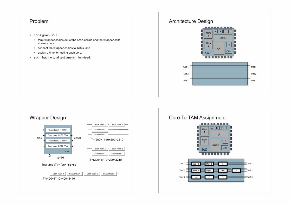
Problem
For a given SoC: form wrapper chains out of the scan-chains and the wrapper cells
at every core
connect the wrapper chains to TAMs, and assign a time for testing each core,
such that the total test time is minimized.
Architecture Design
Mem 1
A
Mem 2
B C D
Logic 1
Logic 2
E
CPUSoC
TAM 1
TAM 2
TAM 3
TAM 1
TAM 2
TAM 3
Wrapper Design
Scan chain 0 (100 FFs)
Scan chain 1 (100 FFs)
SE
SI[0:3] SO[0:3]
Core1
Scan chain 2 (100 FFs)
Scan chain 3 (100 FFs)
Scan chain 0 Scan chain 1 Scan chain 2 Scan chain 3
Scan chain 0 Scan chain 2
Scan chain 0 Scan chain 1
Scan chain 2
Scan chain 3
Scan chain 1 Scan chain 3
T=(400+1)*10+400=4410
Test time (T) = (sc+1)*p+sc
T=(200+1)*10+200=2210
T=(200+1)*10+200=2210
p=10
Core To TAM Assignment
Mem 1
A
Mem 2
B C D
Logic 1
Logic 2
E
CPUSoC
Logic 2
TAM 1
TAM 2
TAM 3
TAM 1
TAM 2
TAM 3
Logic 1
Mem 2
Mem 1
CPU
A
B C D
E
Outline
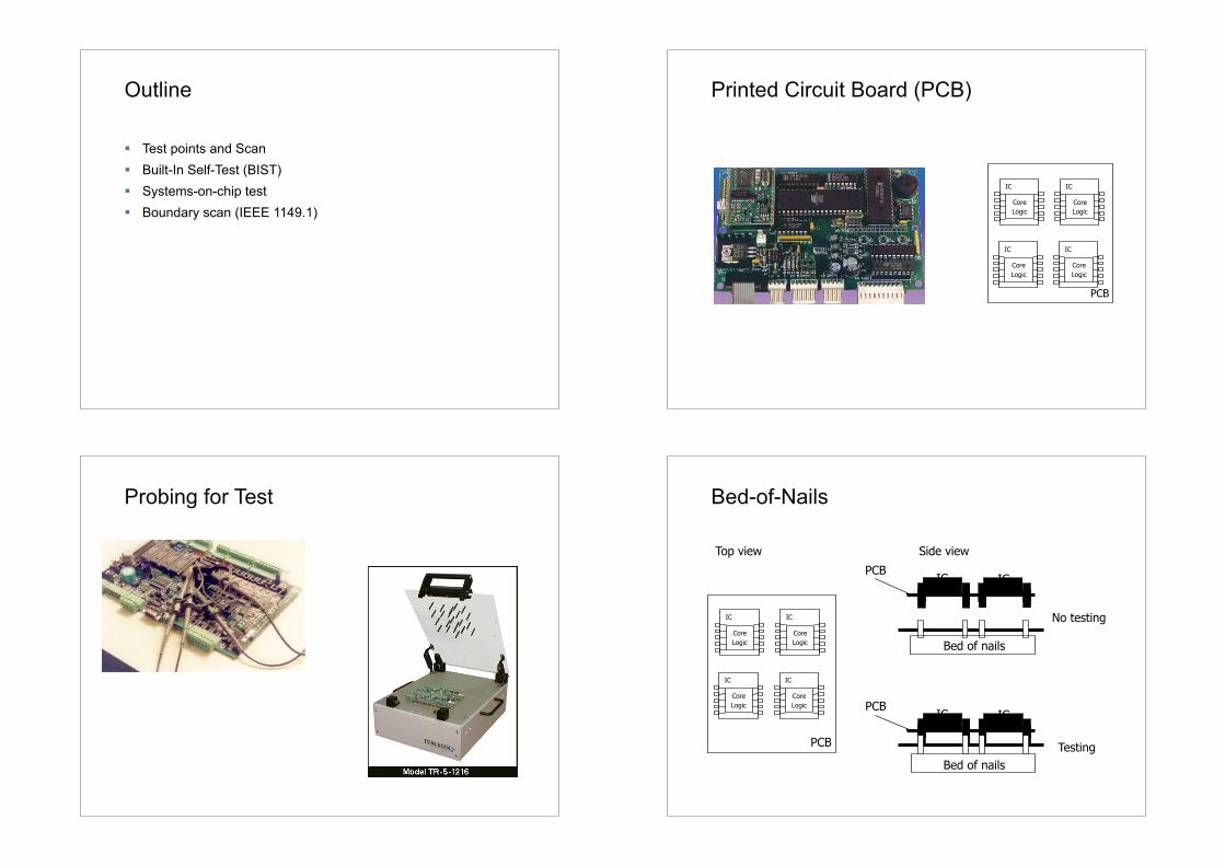
Test points and Scan Built-In Self-Test (BIST) Systems-on-chip test Boundary scan (IEEE 1149.1)
Printed Circuit Board (PCB)
PCB
IC
CoreLogic
IC
CoreLogic
IC
CoreLogic
IC
CoreLogic
Probing for Test Bed-of-Nails
PCB
IC
CoreLogic
IC
CoreLogic
IC
CoreLogic
IC
CoreLogic
IC
Top view Side view
ICPCB
IC ICPCB
Bed of nails
Bed of nailsTesting
No testing

Test Objectives
Given a Printed Circuit Board (PCB) composed of a set of components (ICs) where each component is tested good.
The main objectives are to ensure that all components are: correct (the desired ICs are selected) mounted correctly at the right place on the board and ensuring that interconnections are functioning according to
specification
Problems that may occur: A component does not contain logic A component is not placed where it should be,
A component is at its place but turned wrongly, A component is correct but the interconnection is not correct, for
example due to bad soldering.
Boundary Scan (IEEE std. 1149.1)
The Joint European Test Action Group (JETAG), formed in mid-80, became Joint Test Action Group (JTAG) in 1988 and formed the IEEE std 1149.1. The standard consists of: Test Access Port (TAP)
TAP Controller (TAPC), Instruction Register (IR), and
Data Registers (DR)
20
Boundary Scan
Core logic Core logic
BSC
TRST
TAP Controller
TDI
TMSTCK
BSC
TDO
BSC
BSC
BSC
BSC
BSC
BSC
Instruction Register
Bypass
IEEE Std. 1149.1 and IEEE Std. 1500
Core logic
BSC
TRST
TAP Controller
TDI
TMSTCK
BSC
TDO
BSC
BSC
BSC
BSC
BSC
BSC
Instruction Register
Bypass
wrapper
Core
(User-defined WPP = WPI+WPO+WPC)
Test enable
FI
FI
FO
FO
FI
FO
FI
FO
WFI
WFO
WBY
WFO
WFI
WSOWSI WIR
WBR
WBR
WBR
WBR
WSC: WRCK, WRST, SelectWR, ShiftWR, CaptureWR, UpdateWR
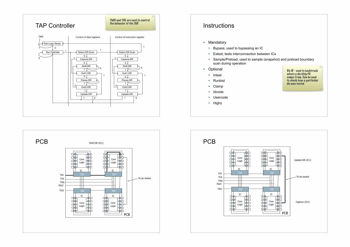
TAP Controller
Select-DR-Scan
Test-Logic-Reset
Run-Test/Idle
Capture-DR
Shift-DR
Exit1-DR
Pause-DR
Exit2-DR
Update-DR
Select-DR-Scan
Capture-DR
Shift-DR
Exit1-DR
Pause-DR
Exit2-DR
Update-DR
1
Control of data registers Control of instruction register
1
1 1
1
11
1 1
1 1
1
0 0
0 0
0
1
0
00
00
1 1
0
1 0
TMS
0 0
TMS and TCK are used to control the behavior of the TAP. Instructions
Mandatory Bypass; used to bypassing an IC
Extest; tests interconnection between ICs Sample/Preload; used to sample (snapshot) and preload boundary
scan during operation
Optional Intest Runbist
Clamp Idcode Usercode
Highz
Die ID - used to backtrack where a die/chip/IC comes from. Can be used to check how a particular die was tested
PCB
PCB
TDI
TCK
TRST
IC
CoreLogic
TDO
IC
CoreLogic
IC
CoreLogic
IC
CoreLogic
TMS
TAP
TAP
TAP
TAP
To be tested
Shift-DR (IC1) PCB
PCB
TDI
TCK
TRST
IC
CoreLogic
TDO
IC
CoreLogic
IC
CoreLogic
IC
CoreLogic
TMS
TAP
TAP
TAP
TAP
To be tested
Update-DR (IC1)
Capture (IC2)

PCB
PCB
TDI
TCK
TRST
IC
CoreLogic
TDO
IC
CoreLogic
IC
IC
TMS
TAP
TAP
TAP
TAP
To be tested
Shift-DR (IC2)CoreLogic
CoreLogic
Scan and MBIST support with Boundary Scan
TDI
TMSTCK TDO
TAP Controller
Scan path
Logic
BISTdecoder
Scan decoder
Instruction register
Decoder
MUX
CompressorMemory
Sca
n_en
Sca
n_in
Sca
n_ou
t
Int_scan
Mbist
Bis
t_so
BISTcontroller
Bist_sel
Introduction
Backplane
Ring Architecture with Shared TMS
TDI
TCK
TMS
TRST
TDO
PCB
ICCoreLogic
ICCoreLogic
ICCoreLogic
ICCoreLogic
PCB
ICCoreLogic
ICCoreLogic
ICCoreLogic
ICCoreLogic
PCB
ICCoreLogic
ICCoreLogic
ICCoreLogic
ICCoreLogic
PCB
ICCoreLogic
ICCoreLogic
ICCoreLogic
ICCoreLogic

TDITCK
TMS2
TRSTTDO
TMS3
TMS1
TMS4
PCB
ICCoreLogic
ICCoreLogic
ICCoreLogic
ICCoreLogic
PCB
ICCoreLogic
ICCoreLogic
ICCoreLogic
ICCoreLogic
PCB
ICCoreLogic
ICCoreLogic
ICCoreLogic
ICCoreLogic
PCB
ICCoreLogic
ICCoreLogic
ICCoreLogic
ICCoreLogic
Ring Architecture with Separate TMS Star Architecture
PCB
ICCoreLogic
ICCoreLogic
ICCoreLogic
ICCoreLogic
PCB
ICCoreLogic
ICCoreLogic
ICCoreLogic
ICCoreLogic
PCB
ICCoreLogic
ICCoreLogic
ICCoreLogic
ICCoreLogic
PCB
ICCoreLogic
ICCoreLogic
ICCoreLogic
ICCoreLogic
TDITCKTMSTDO
TDITCKTMSTDO
TDITCKTMSTDO
TDITCKTMSTDO
Multi-drop Architecture
PCB
ICCoreLogic
ICCoreLogic
ICCoreLogic
ICCoreLogic
PCB
ICCoreLogic
ICCoreLogic
ICCoreLogic
ICCoreLogic
PCB
ICCoreLogic
ICCoreLogic
ICCoreLogic
ICCoreLogic
PCB
ICCoreLogic
ICCoreLogic
ICCoreLogic
ICCoreLogic
TDITCKTMSTDO
Bus master
Multi-Drop Device
Multi-Drop Device
Multi-Drop Device
Multi-Drop Device
IEEE 1149 Standard Family
Number Main objectives Status
1149.1 Testing of digital chips and interconnects between chips
Std. 1149.1-1990
Std. 1149.1a-1993
Std. 1149.1b-1994 (BSDL)
Std. 1149.1-2001
1149.2 Extended digital serial interface Discontinued
1149.3 Direct access testability interface Discontinued
1149.4 Mixed-signal test bus Std. 1149.4-1999
1149.5 Standard module test and maintenance (MTM) bus
Std. 1149.5-1995 (not endorsed by IEEE since 2003)
1149.6 High-speed network interface protocol Std. 1149.6-2003
1149.7 Reduced-Pin and Enhanced-Functionality Test Access Port Std.1149.7-2009

Introduction to structured VLSI design
Design for Test (DfT) - Part 2Erik Larsson
EIT, Lund University