the ct-pps project: detector hardware and operational
TRANSCRIPT

PoS(Vertex 2017)015
The CT-PPS project: detector hardware andoperational experience
F. Ravera∗, on behalf of the CMS and TOTEM CollaborationsUniversity of Genova, INFN GenovaE-mail: [email protected]
The CMS-TOTEM Precision Proton Spectrometer allows extending the LHC physics program bymeasuring protons in the very forward regions of CMS. Tracking and timing detectors have beeninstalled along the beam pipe at∼ 210 m from the CMS interaction point on both sides of the LHCtunnel. The tracking system consists of a station of silicon strip detectors and one of silicon pixeldetectors on each side. The latter is composed of six planes of 3D silicon pixel sensors bump-bonded to the PSI46dig ROC developed for the CMS Phase I Pixel Tracker upgrade. A trackresolution of ∼ 10 µm is obtained. The future goal is to replace the present strip stations withpixel ones in order to ensure better multi-track reconstruction. Each timing station is made of threeplanes of diamond detectors and one plane equipped with an Ultra-Fast Silicon Detector (UFSD).A timing resolution of a few tens of picoseconds can be achieved with the present detector; alarge R&D effort is ongoing to reach the 10 ps target resolution. This contribution describes thehardware characteristics and the present status of the CT-PPS project. The operational experienceduring the 2017 data taking is also presented.
The 26th International Workshop on Vertex Detectors10-15 September, 2017Las Caldas, Asturias, Spain
∗Speaker.
c© Copyright owned by the author(s) under the terms of the Creative CommonsAttribution-NonCommercial-NoDerivatives 4.0 International License (CC BY-NC-ND 4.0). https://pos.sissa.it/
PoS(Vertex 2017)015
The CT-PPS project: detector hardware and operational experience F. Ravera
1. Introduction
The aim of the CMS-TOTEM Precision Proton Spectrometer (CT-PPS) project [1] is the mea-surement of Central Exclusive Production (CEP) in the standard, high-luminosity fills at the LargeHadron Collider (LHC). CEP in proton-proton collisions, namely the process pp→ pX p, can bedriven by a photon-photon interaction or double Pomeron exchange. The advantage of measuringthis reaction is that, by reconstructing the two leading protons and specifically their fractional mo-mentum loss (ξ ) and four-momentum transfer squared (t), the full event is measured and strongconstraints can be imposed on the object X reconstructed by the central CMS detector.
CT-PPS already acquired data in 2016 with an “accelerated program” and with ∼ 10 of the∼ 15 fb−1 collected, the first measurement of semi-exclusive dimuon production at the LHC ener-gies has been published [2]. From the reconstructed proton it is possible to constrain the dimuonkinematics, allowing a strong suppression of the backgrounds, mainly due to Drell-Yan dimuonsand pile-up protons. Thanks to that, with the only 12 events observed a significance of 4.3σ hasbeen reached. This analysis, together with proving the effectiveness of the CT-PPS detector, showsalso the discover potential of adding a near-beam proton spectrometer to the experiments at LHC.
2. The CT-PPS detector
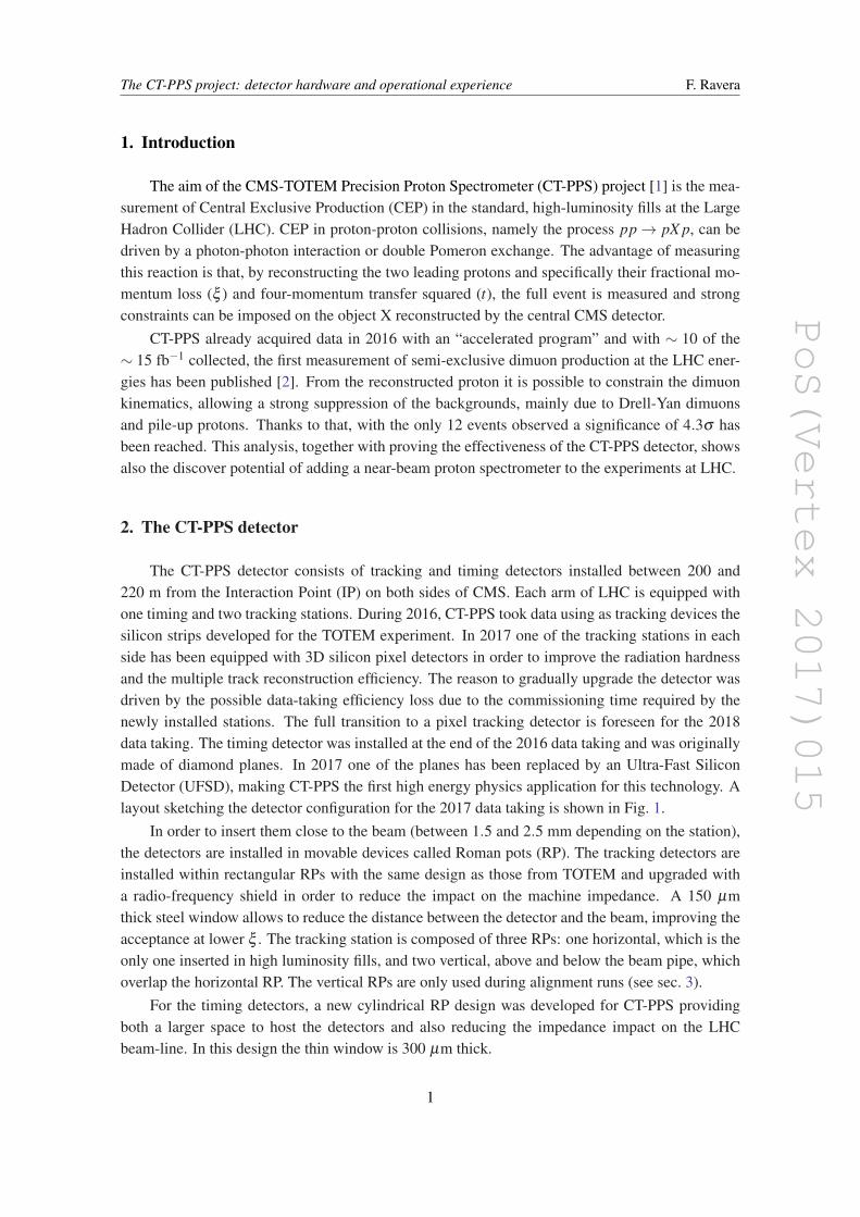
The CT-PPS detector consists of tracking and timing detectors installed between 200 and220 m from the Interaction Point (IP) on both sides of CMS. Each arm of LHC is equipped withone timing and two tracking stations. During 2016, CT-PPS took data using as tracking devices thesilicon strips developed for the TOTEM experiment. In 2017 one of the tracking stations in eachside has been equipped with 3D silicon pixel detectors in order to improve the radiation hardnessand the multiple track reconstruction efficiency. The reason to gradually upgrade the detector wasdriven by the possible data-taking efficiency loss due to the commissioning time required by thenewly installed stations. The full transition to a pixel tracking detector is foreseen for the 2018data taking. The timing detector was installed at the end of the 2016 data taking and was originallymade of diamond planes. In 2017 one of the planes has been replaced by an Ultra-Fast SiliconDetector (UFSD), making CT-PPS the first high energy physics application for this technology. Alayout sketching the detector configuration for the 2017 data taking is shown in Fig. 1.
In order to insert them close to the beam (between 1.5 and 2.5 mm depending on the station),the detectors are installed in movable devices called Roman pots (RP). The tracking detectors areinstalled within rectangular RPs with the same design as those from TOTEM and upgraded witha radio-frequency shield in order to reduce the impact on the machine impedance. A 150 µmthick steel window allows to reduce the distance between the detector and the beam, improving theacceptance at lower ξ . The tracking station is composed of three RPs: one horizontal, which is theonly one inserted in high luminosity fills, and two vertical, above and below the beam pipe, whichoverlap the horizontal RP. The vertical RPs are only used during alignment runs (see sec. 3).
For the timing detectors, a new cylindrical RP design was developed for CT-PPS providingboth a larger space to host the detectors and also reducing the impedance impact on the LHCbeam-line. In this design the thin window is 300 µm thick.
1
PoS(Vertex 2017)015
The CT-PPS project: detector hardware and operational experience F. Ravera
Figure 1: Sketch of the CT-PPS detector configuration for the 2017 data taking.
Both types of Roman pots are inserted in high luminosity fills at 12 beam sigmas plus a safetymargin of 0.3 mm. The detectors within the pot are placed in a secondary vacuum in order toreduce the stress on the thin window, which on the other side faces the high vacuum of the LHCbeam-pipe.
2.1 The tracking detector
By measuring the proton tracks at the RP positions it is possible to determine the protonkinematics at the IP by means of the so-called beam optics, which provides a parametrization ofthe LHC magnetic lattice between the IP and the RPs.
Because of the small distance from the LHC beam at which the detectors are operating, goodradiation hardness is required. The simulations indicate that for 100 fb−1 a maximum flux ofthe order of ∼ 5× 10¹⁵ proton/cm2 is expected, which corresponds to fluences between 1 and3× 1015 neq/cm2. Besides the radiation hardness, another requirement is the reduction of theinsensitive area at the sensor edge facing the beam, in order to increase the acceptance to lowermasses of the centrally produced state.
Tracking sensors are operated at ∼ −20◦C in order to mitigate the increase of the leakagecurrent due to the irradiation. Therefore, to avoid condensation, the pressure in the tracking RPs iskept below 20 mbar.
The baseline design of the CT-PPS tracking detector foresees to use 3D pixel sensors thatprovide an intrinsic radiation hardness and the possibility of effectively implementing slim edges.In the following sections the design and the production of the 3D modules for CT-PPS is describedalong with the strip detectors used for the first years of data taking.
2
PoS(Vertex 2017)015
The CT-PPS project: detector hardware and operational experience F. Ravera
2.1.1 TOTEM strip detector
The TOTEM strip detectors were developed with a n-in-p micro-strip edgeless technology ona 300 µm silicon substrate [3]. Current terminating rings around the active area of the sensor areimplemented in order to collect the large current generated in the highly damaged sensor edge, andreduce the insensitive area down to 50 µm. The strips, oriented at ±45◦ with respect to the edgecloser to the beam, have a pitch of 66 µm and are binary read-out with the VFAT2 ReadOut Chip(ROC) [5].
The tracking station is equipped with 5 units each made of two strip sensors with oppositestrip orientation. A track resolution of 10 µm is reached in both x and y directions. Apart fromthe limitations in reconstructing events with multiple tracks, the silicon strip sensors were qualifiedfor a radiation hardness equivalent to few fb−1 [4]. The data collected in 2016 confirmed that,by operating at a higher bias voltage, values of the sensor efficiency as high as ∼ 80% could berestored in the mm2 area with the highest occupancy. The detectors were anyway replaced after∼ 10 fb−1 to restore optimal performance
The back-end electronics and the data acquisition (DAQ) software are the same as those of theTOTEM experiment and were integrated into the CMS DAQ system at the beginning of 2016.
2.1.2 3D pixel detector
The basic concept of the 3D sensors [6] is that, instead of implementing the electrodes onthe two wafer surfaces like it is done for the standard planar technology, they are etched in acolumn perpendicularly to the surface towards the silicon bulk. This design allows to decouple thedetector thickness, which is proportional to the charge deposited by a crossing particle, and theinter-electrode distance. This provides several advantages: lower depletion voltage, faster chargecollection and high charge collection efficiency after irradiation.
Several beam tests and irradiation campaigns have been carried out on the 3D sensors fromdifferent vendors - CNM (Barcelona, Spain), FBK (Trento, Italy) and SINTEF (Oslo, Norway) -and the suitability of this technology for CT-PPS has been confirmed. The order was eventuallyplaced with CNM.
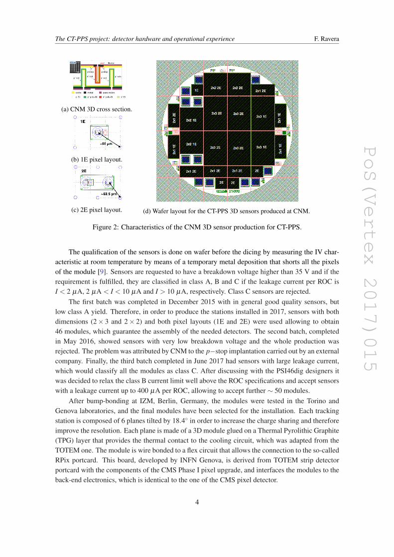
The CNM sensors for CT-PPS have been implemented in a double-sided non-passing-throughtechnology, meaning that n+ and p+ electrodes are etched from opposite surfaces of the wafer andthey stop before reaching the other surface (see Fig. 2a). The sensors have been built on a 230 µmthick wafer and the columns are 200 µm deep. A 200 µm slim edge is implemented with p−typecolumn fences surrounding the sensitive area. By increasing the bias voltage, the inefficient edgecan be reduced down to 50 µm [7].
The production of the 3D sensors has been divided into three batches of 12 wafers whoselayout is shown in Fig. 2d. The sensors are designed to be read out by the PSI46dig ReadOut Chip(ROC), the same used for the CMS Phase I pixel detector [8], which is made of a 52×80 matrix ofpixels with size 150×100 µm2. The baseline design for CT-PPS is a 2E pixel configuration (tworeadout columns for every pixel as shown in Fig. 2c) and 2×3 sensors, which means readout by 6ROCs. However, also 1E (one readout column for every pixel as shown in Fig. 2b) and 2×2 sensorsare included in the wafer design as a backup solution. In the layout also single-ROC sensors arepresent and used for validating the production on beam [7].
3
PoS(Vertex 2017)015
The CT-PPS project: detector hardware and operational experience F. Ravera
(a) CNM 3D cross section.
(b) 1E pixel layout.
(c) 2E pixel layout. (d) Wafer layout for the CT-PPS 3D sensors produced at CNM.
Figure 2: Characteristics of the CNM 3D sensor production for CT-PPS.
The qualification of the sensors is done on wafer before the dicing by measuring the IV char-acteristic at room temperature by means of a temporary metal deposition that shorts all the pixelsof the module [9]. Sensors are requested to have a breakdown voltage higher than 35 V and if therequirement is fulfilled, they are classified in class A, B and C if the leakage current per ROC isI < 2 µA, 2 µA < I < 10 µA and I > 10 µA, respectively. Class C sensors are rejected.
The first batch was completed in December 2015 with in general good quality sensors, butlow class A yield. Therefore, in order to produce the stations installed in 2017, sensors with bothdimensions (2× 3 and 2× 2) and both pixel layouts (1E and 2E) were used allowing to obtain46 modules, which guarantee the assembly of the needed detectors. The second batch, completedin May 2016, showed sensors with very low breakdown voltage and the whole production wasrejected. The problem was attributed by CNM to the p−stop implantation carried out by an externalcompany. Finally, the third batch completed in June 2017 had sensors with large leakage current,which would classify all the modules as class C. After discussing with the PSI46dig designers itwas decided to relax the class B current limit well above the ROC specifications and accept sensorswith a leakage current up to 400 µA per ROC, allowing to accept further ∼ 50 modules.
After bump-bonding at IZM, Berlin, Germany, the modules were tested in the Torino andGenova laboratories, and the final modules have been selected for the installation. Each trackingstation is composed of 6 planes tilted by 18.4◦ in order to increase the charge sharing and thereforeimprove the resolution. Each plane is made of a 3D module glued on a Thermal Pyrolithic Graphite(TPG) layer that provides the thermal contact to the cooling circuit, which was adapted from theTOTEM one. The module is wire bonded to a flex circuit that allows the connection to the so-calledRPix portcard. This board, developed by INFN Genova, is derived from TOTEM strip detectorportcard with the components of the CMS Phase I pixel upgrade, and interfaces the modules to theback-end electronics, which is identical to the one of the CMS pixel detector.
4
PoS(Vertex 2017)015
The CT-PPS project: detector hardware and operational experience F. Ravera
Two pixel detector packages were mounted at CERN and tested in the same conditions ofcooling and secondary vacuum as those present along the LHC beam line. The two RP unitswere installed along the LHC beam-pipe in March 2017 during the extended year-end technicalstop (EYETS). At the same time the DAQ software was developed and integrated in the CMScentral DAQ. By means of the ROC internal calibration circuit, the detector was fully calibratedand optimized for data taking. The read-out threshold was set to∼ 2000 e− and the spread betweenpixels was measured to be ∼ 135 e−. The percentage of bad channels, defined as those withefficiency lower than 90% in measuring a charge of ∼ 5000 e−, is less that 0.05%.
2.2 The timing detector
CT-PPS has to operate in high luminosity at LHC with up to 50 pile-up interactions per bunchcrossing. It is therefore crucial to associate the protons measured with CT-PPS with the vertexreconstructed in CMS, especially in the cases in which the central detector does not reconstructall the final-state products (neutrinos or beyond standard model objects) and the kinematic cutsconstraining the central system and the proton are less effective. In order to achieve this, a “z-by-timing” method is used, based on the measurement of the difference of arrival times of thetwo protons in opposite directions. In particular, with a 10 ps timing resolution, a vertex positionresolution of σz ∼ 2 mm can be obtained, which would allow to strongly suppress the pile-up-induced backgrounds.
Due to the higher voltage at which the diamond detectors are operated (∼ 500 V), the pressurein the timing RPs is set between 100 and 110 mbar in order to avoid discharging. For this reasonthe temperature of the cooling circuit is set to 15◦C.
Both technologies are connected to a discrete-component amplifier that shapes the signal tobe fed into the NINO amplifier [10], whose output is then digitized by the High-Precision Time-to-Digital Converter (HPTDC) [11], which provides the measurement of the leading and trailing edgeallowing for the time-walk correction. The coded signal is then handled by an FPGA close to thedetector that encodes the data and sends them to the back-end electronics, which is adapted fromthe TOTEM one.
In order to reach the target resolution, the detector must be synchronized with a clock withjitter of the order of few ps. The present detector has two different systems that can provide theprecise clock: the Universal Picosecond Timing System based on an optical network and an RF-feedback with low-loss coaxial cable. Both systems showed comparable figures of merit.
Each timing station is equipped with four planes of timing detectors. While in 2016 all theplanes were equipped with diamond detectors, in 2017 each station consists of three diamond andone Ultra-Fast Silicon Detector (UFSD) planes.
2.2.1 Diamond detector
Each of the three diamond planes is made of four 4×4 mm2 single crystals produced by chem-ical vapor deposition. The diamond sensors were grown to a thickness of 500 µm by Element SixLtd., Ascot, UK, and the metallization of the pads was done at Applied Diamond, Inc., Wilming-ton, USA, and PRISM, the Princeton University laboratory. Each of the four crystals of the planehas a different segmentation along the x direction in order to equalize the channel occupancy andhence smaller pads are present closer to the beam. Crystals with the same segmentation are glued
5
PoS(Vertex 2017)015
The CT-PPS project: detector hardware and operational experience F. Ravera
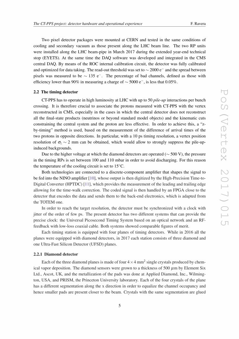
with different orientation and position between planes to improve the x-resolution to ∼ 150 µmand allow a rough track reconstruction. The orientation of the diamond pads is visible in the plotsof Fig.4
The timing resolution measured on beam is ∼ 80 ps per plane [12] and since the technology isintrinsically radiation hard, the sensors are expected to withstand the whole proton flux CT-PPS isexpected to be exposed to.
2.2.2 UFSD
The UFSD sensors installed in CT-PPS were produced at CNM; they have an active thicknessof 50 µm. The sensor pads have been adapted to couple with the diamond plane readout and henceeight 0.5×6 mm2 and four 1×3 mm2 pads are presently connected (see Fig.4).
This kind of technology showed on beam a timing resolution of ∼ 35 ps [13]. The radiationhardness for the UFSD is still an issue and they are expected to withstand up to∼ 1014 proton/cm2.Significant R&D on this aspect is ongoing.
3. Operational experience and status of the data taking
An integral part of the CT-PPS data taking are the so-called alignment runs. This special runhas multiple goals: RP alignment with respect to the collimators, relative alignment between theRPs, alignment with respect to the beam and optics determination.
The procedure starts by closing the collimators upstream of the detector to few beam sigmas(between 5 and 8.5) and afterwards slowly approaching one by one the RPs to the beam. Whena spike is observed in the Beam Loss Monitors (BLM) downstream of the detector the pot hasreached the same position as the collimators in terms of beam sigmas. At this point the collimatorsare opened and the data taking starts.
The relative alignment between the RPs is determined by the tracks passing in the overlap re-gions of the vertical and horizontal pots, while the alignment with respect to the beam is performedby analysing the hit distributions from protons in elastic scattering events in the vertical detectorsand in diffractive events in the horizontal detectors. Finally, the tuning of the optics, which isfundamental for the proton kinematic reconstruction, is obtained by analysing the hit distributionshape in the horizontal tracking detectors. While the global alignment for the 2017 has alreadybeen determined, the optics parameter tuning requires a more refined analysis that is currently inprogress.
In Fig. 3 the track x and y coordinates are shown for the two tracking stations on each side ofCMS. Although the coordinates are expressed in arbitrary systems of reference for each Roman pot,the halo visible on the vertical pots (top and bottom) corresponds to the edge of the hit distributionin the horizontal RP, confirming the overlap of the detectors, a fundamental requirement for thealignment studies. It is also worth noticing that this is the first time the CT-PPS pixel detector tookdata as a subdetector of CMS.
Even if the timing detector is still in a commissioning phase, it has been possible to verifythe consistency of the data collected so far. In order to do that, Fig. 4 shows for each of theplanes installed on one of the two arms the hit maps measured in the strip detector by requiringa coincidence in the timing plane considered (similar plots are obtained for the opposite side).
6

PoS(Vertex 2017)015
The CT-PPS project: detector hardware and operational experience F. Ravera
Figure 3: Track position distribution on the tracking CT-PPS detectors during the alignment run.
Despite the low statistics, one can recognize the expected hit distribution as shown in the trackingdetectors (Fig. 3) convoluted with the timing plane acceptances, which indicates that the sensorsare centered on the vertical beam position. The different entry colors correspond to different firedchannels of the plane allowing also to verify that the detectors are correctly mapped.
As already mentioned, CT-PPS took data also in 2016 and collected data corresponding to anintegrated luminosity of ∼ 15 fb−1. In 2017, after the alignment run, the Roman Pots have beeninserted during the LHC intensity ramp-up and certified for insertion up to the maximum 2017luminosity with 2556 bunches. After this step, they have been inserted in all the high luminosityfills of the year and recorded ∼ 40 fb−1 (non official number). The detector ran stably during thewhole data taking with minimum impact on the CMS data acquisition.
4. Conclusions
The current CT-PPS detector has been installed in April 2017 and is composed of four differ-ent detector technologies: silicon strips, silicon 3D pixels, scCVD diamonds and UFSDs. All thedetectors have been successfully integrated in the CMS DAQ since the first fill of 2017. The 3Dpixel tracker, which constitutes the first application of this technology in CMS, has been commis-sioned. The timing detector system, which includes the first application of UFSD in a high energyphysics experiment, has shown to meet expectations. A full analysis of its performance is currentlyongoing. So far CT-PPS recorded ∼ 55 fb−1 and 10 fb−1 of them have been analyzed to produceits first physics result. CT-PPS is foreseen to collect data in 2018 with a full 3D pixel tracker thatwill further improve the performance in order to reach the 100 fb−1 design target.
7
PoS(Vertex 2017)015
The CT-PPS project: detector hardware and operational experience F. Ravera
Figure 4: Hit maps as measured in the strips are plotted requiring a coincidence with timingdetectors. Different colors correspond to different channels fired on the plane. As a comparison,the corresponding pad layout is shown.
Acknowledgment
Special thanks go to the CT-PPS group for the great commitment that allowed the success ofthe installation and data taking. We would also like to express our gratitude to the 26th InternationalWorkshop on Vertex Detectors for inviting us to present the CT-PPS project.
References
[1] The CMS and TOTEM Collaborations, CMS-TOTEM Precision Proton Spectrometer,CERN-LHCC-2014-021 (2014)
[2] The CMS and TOTEM Collaborations, Evidence for proton-tagged, central semi-exclusive productionof high-mass muon pairs at 13 TeV with the CMS-TOTEM Precision Proton Spectrometer,CMS-PAS-PPS-17-001, TOTEM-NOTE-2017-003 (2017)
[3] The TOTEM Collaboration, Final size planar edgeless silicon detectors for the TOTEM experiment,Nucl. Instrum. Meth. A563 (2006), 41
[4] G. Ruggiero et al. Characteristics of edgeless silicon detectors for the Roman Pots of the TOTEMexperiment at the LHC, Nucl. Instrum. Meth. A604 (2009), 242
[5] P.Aspell et al., VFAT2: A front-end system on chip providing fast trigger information, digitized datastorage and formatting for charge readout of multi-channel silicon and gas particle detectors,Electronics for particle physics. Proceedings, Topical Workshop, TWEPP-07, Prague, CzechRepublic, September 3-7 (2007), 67
8
PoS(Vertex 2017)015
The CT-PPS project: detector hardware and operational experience F. Ravera
[6] S. Parker et al., 3-D: A New architecture for solid state radiation detectors, Nucl. Instrum. Meth. A395 (1997), 328
[7] F. Ravera, The CT-PPS tracking system with 3D pixel detectors, JINST 11 (2016) C11027
[8] The CMS Collaboration, CMS Technical Design Report for the Pixel Detector Upgrade,CERN-LHCC-2012-016 (2012)
[9] C. Da Via et al., 3D Silicon Sensors: Design, Large Area Production and Quality Assurance for theATLAS IBL Pixel Detector Upgrade, Nucl. Instrum. Meth. A694 (2012) 321
[10] F. Anghinolfi et al., NINO: an ultra-fast and low-power front-end amplifier/discriminator ASICdesigned for the multigap resistive plate chamber, Nucl. Instrum. Meth. A533 (2004) 183
[11] M. Mota and J. Christiansen, A high-resolution time interpolator based on a delay locked loop and anRC delay line, IEEE JSSC 34 (1999) 1360
[12] G Antchev et al., Diamond detectors for the TOTEM timing upgrade, JINST 12 (2017) P03007
[13] N. Cartiglia et al., Beam test results of a 16 ps timing system based on ultra-fast silicon detectors,Nucl. Instrum. Meth. A850 (2017) 83
9