the future of technology - 50 years ahead … future of technology - 50 years ahead ken gilleo, ......
TRANSCRIPT
1
THE FUTURE OF TECHNOLOGY - 50 YEARS AHEAD Ken Gilleo, PhD
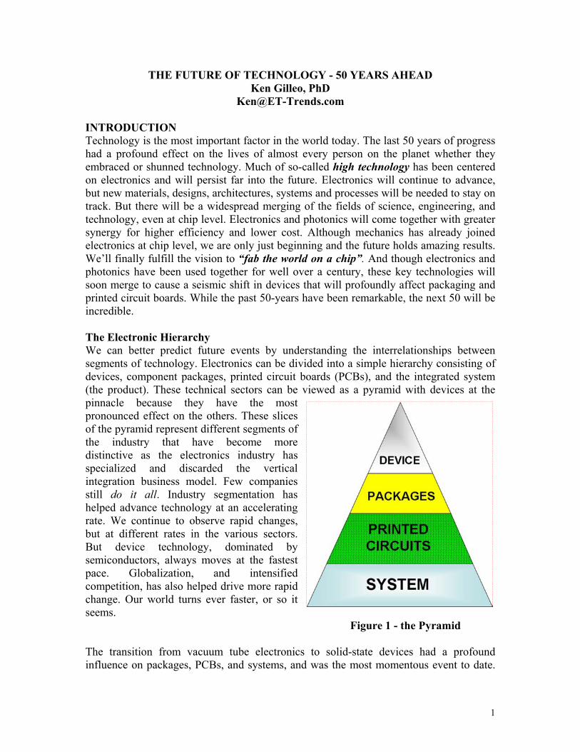
[email protected] INTRODUCTION Technology is the most important factor in the world today. The last 50 years of progress had a profound effect on the lives of almost every person on the planet whether they embraced or shunned technology. Much of so-called high technology has been centered on electronics and will persist far into the future. Electronics will continue to advance, but new materials, designs, architectures, systems and processes will be needed to stay on track. But there will be a widespread merging of the fields of science, engineering, and technology, even at chip level. Electronics and photonics will come together with greater synergy for higher efficiency and lower cost. Although mechanics has already joined electronics at chip level, we are only just beginning and the future holds amazing results. We’ll finally fulfill the vision to “fab the world on a chip”. And though electronics and photonics have been used together for well over a century, these key technologies will soon merge to cause a seismic shift in devices that will profoundly affect packaging and printed circuit boards. While the past 50-years have been remarkable, the next 50 will be incredible. The Electronic Hierarchy We can better predict future events by understanding the interrelationships between segments of technology. Electronics can be divided into a simple hierarchy consisting of devices, component packages, printed circuit boards (PCBs), and the integrated system (the product). These technical sectors can be viewed as a pyramid with devices at the pinnacle because they have the most pronounced effect on the others. These slices of the pyramid represent different segments of the industry that have become more distinctive as the electronics industry has specialized and discarded the vertical integration business model. Few companies still do it all. Industry segmentation has helped advance technology at an accelerating rate. We continue to observe rapid changes, but at different rates in the various sectors. But device technology, dominated by semiconductors, always moves at the fastest pace. Globalization, and intensified competition, has also helped drive more rapid change. Our world turns ever faster, or so it seems. Figure 1 - the Pyramid The transition from vacuum tube electronics to solid-state devices had a profound influence on packages, PCBs, and systems, and was the most momentous event to date.

2
We only need to compare the early massive, power-hungry, console radios to the latest wearable products, to appreciate the importance of change at the device level. But it took about 50 years to move from tubes to transistors. We should expect a major device change every 50-years; the IC was invented in 1958. We are due for a major event! Although present semiconductor technology is predicted to meet our seemingly insatiable demands for a decade or more, new devices made of different materials will be housed in novel packages, connected to PCBs that are much different from today’s, to produce extremely small and powerful products. Let’s look at the goals, challenges, and solutions for the future. Century of Progress Surprising perhaps, the challenges for the next 50 years are more or less the same as those of the past 50. In fact, the goals and challenges have not really changed since the beginning. Throughout the First Century of Electronics, scientists and technologists were tasked with grand challenges that remain as guideposts as we travel into the future. These key criteria are: Grand Challenges
Density (smaller) Performance (faster) Cost - value (cheaper) (Addition of other technologies to electronics at the device level)
These fundamental challenges can be applied to our basic segments shown in the pyramid; the device, package, printed circuit, and total system. Density has been at the top of the task list from the beginning - even when the original “high tech” products, like the telegraph and telephone, were based on electricity. High tech began, at least for our purposes, as the Telecom Revolution launched in the late 1800’s. This incredible revolution continues today, and telecom has moved to the top as the most important driver for technical advancement. The first printed circuit patent [1] set the stage by defining the first goal, “…it is desirable to have a large number of conductors…within very small compass….” The same statement is equally true today! We’ve come a long way since 1903, but the next few decades will seem amazing even to the most forward thinking optimists. So get ready to bust myths, slaughter sacred cows, and make tried and true technology obsolete. Expect future advances to replace copper - the king of conductors, eliminate silicon - the incumbent semiconductor, and to even replace the venerable electron as the workhorse messenger. Solder, the 7,000-year old [2-4] “glue of electronics” will also be retired. Indeed, we are in for serious disruptive changes. So put down your roadmap and welcome to detour into the future. Devices Let’s begin with the device, with its top-of-the-pyramid, high-leverage position, that significantly affects everything else. Today, semiconductor devices are fabricated using a sequence of processes carried out in sealed massive chambers under precisely controlled conditions, in ultra-clean atmospheres, using mostly automatic equipment in fabs costing
3
billions of dollars. Device feature sizes now fall within the nano-scale range (1 to 100-nanometers (nm); 1-billionth nm = 1-meter), although these chips should not be defined as Nanoelectronics. Today’s marvelous semiconductor technology enables hundreds of millions of transistors to be crafted on a single postage stamp-size chip usually made from silicon and its compounds. The semiconductor industry continues to increase density in many ways, such as reducing feature dimensions, adding layers, and morphing to more “vertical” architectures. However, silicon-based devices will eventually fall short as demands continually increase. But many scientists, engineers, technologists, business leaders, entrepreneurs, and futurists have high hopes for fundamentally new device technology that will meet needs far into the future. A host of future device strategies are underway that include Nanoelectronics, quantum devices, molecular electronics, single-electron switches, photonic logic engines, and even bio-centric computational machines. Even more concepts are being applied to memory chips. While it can take about 50-years for some of these areas to come to fruition, other high-impact technical breakthroughs are closer. But consider that we have been using silicon-based electronics for nearly a half-century and the forces for change are building. Beyond Silicon Although Nanoelectronics may be the next big thing, there are other contending technologies that are fundamentally different. Nanoelectronics, even if it employs non-silicon materials, is following the “silicon blueprint”. Nano-transistors are here now, and these “organic” devices will soon be connected to form ICs. But they will probably operate using the same principles as today’s silicon-based ICs. The end result will be more dense and powerful chips, but there may not be much change for the other electronic segments. Present packages and PCBs will probably be adequate. In fact, requirements could be lower, but more on that later. We need to include all-photonic and bio-centric computers in our future tech list, and success in either field would be much more disruptive than Nanoelectronics is somewhat analogous to a better engine in the same car model. Over the next 20 to 30 years, we can expect success for all-photonic computing technology, where photons replace electrons in a fundamentally different system. We’ve become so accustomed to charge-based logic and memory technology, that other viable approaches are ignored. Consider that the human brain employs principles that are much different from today’s IC mechanisms. But there is an intermediate step to consider, where electrons handle logic and memory functions and photons will deal with data transmission. We must keep in mind that what happens outside of the chip is just as critical as what happens within. The chip must be efficiently connected to the outside world. Now Enter Silicon Photonics The chargeless photon is the most important information messenger for the Internet, telephones, wireless, and most life forms. Photons carry a wealth of information and can even tell us the chemical composition and speed of distant stars. But the photon has not yet succeeded in solid-state logic and memory devices. So it makes sense to develop a hybrid IC where electronics is used for computations and photonics takes on the messenger task. Internet and telephone hardware was designed to partition the
4
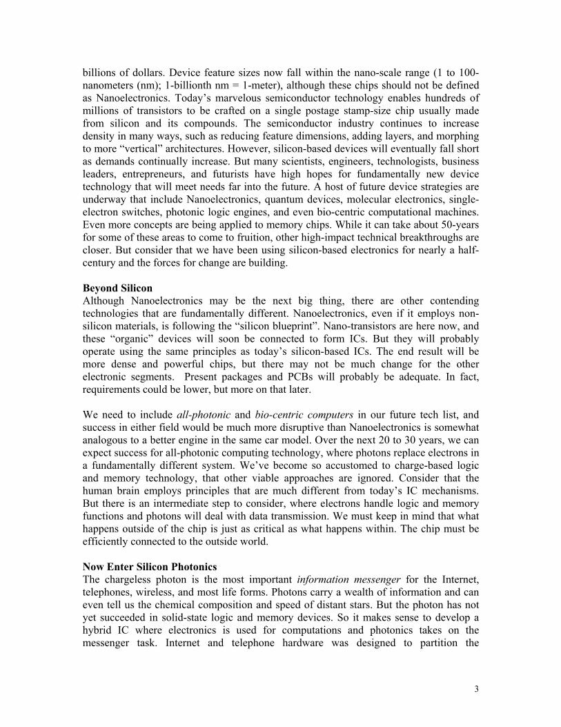
computation/data transmission tasks allowing the photon to handle medium and long-distance transmissions while electronics was retained for switching and control. The world is connected by “optical wires”. The data-laden photons race along glass optical fiber links that circle the globe as underground and submarine cabling. But why photons instead of electrons? Photons, travel through a single thin glass fiber at the speed of light and can carry about 1-million times more information than electrons using a copper wire. Nothing beats the photon for bandwidth and the reasons are due to the fundamental differences of charged electrons vs. neutral wave-differentiated photons. Remarkably, hundreds, or even thousands, of different wavelengths can independently travel through the same thin (9-micron) fiber. Photonics can send hundreds, or even thousands of different wavelengths through a single fiber using powerful wave division multiplexing (WDM) since photons are relatively non-interactive. Could this mega-bandwidth method eliminate the “copper bottleneck” that limits chip-to-chip data transfer by electrons? Many groups have been working on solutions for light-linking electronic chips but the challenges for a cost-effective solution are substantial. Recently, Intel and the University of California - Santa Barbara (UCSB), came up with the last tool for a potent “Photonic Toolkit” that could enable light linking of silicon chips, and finally eliminate the copper bandwidth limitation. This technology was dubbed “Silicon Photonics” and it purports to provide a means for economically fabricating a data-transferring modulating laser onto a silicon chip. The laser will eventually be able to send vast amounts of data into and out of a CPU without electrical connections. There’s more to this than just adding an on-chip laser, but all the blocks of technology are now ready to be combined into a photonic chip system. The final breakthrough, in a succession of many, occurred when the team built the world’s first electrically powered Hybrid Silicon Laser using standard silicon manufacturing processes. The Internet uses rather expensive modules built from discrete components. These researchers were able to marry light-emitting Indium Phosphide (InP) to silicon (Si). The InP and Si layers were combined by wafer-level bonding. Since silicon is transparent to the wavelengths used, it can be fabricated with light-manipulating capabilities such as channels, waveguides, prisms, splitters and frequency-separating diffraction gratings. MEMS fabrication methods could also be used to produce optical structures in silicon. Application of voltage to the InP laser structure produces infrared “light” that travels through the silicon waveguide to create a laser beam that can drive other silicon photonic devices. So we can expect hybrid chips, especially the CPU, to move into the mainstream during the next 4 to 10 years (see Figure 2).
Figure 2 - Photonics Hybrid Chips (Intel)
5
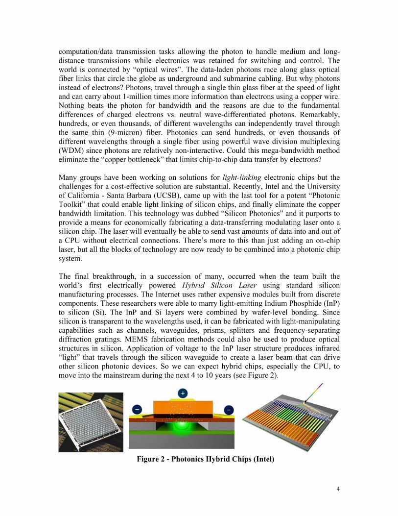
But how will the hybrid chip affect packaging and printed circuits? Surprisingly, the interim chip that combines electrons and photons will have a much more dramatic influence on the other segments of our pyramid than Nanoelectronics that will probably adopt existing technology. But how will chip-to-chip photonic data be transmitted? There are two choices, through the air, called free-space, or through optical channels. Perhaps both methods will be used. Regardless, the chip package will need to provide optical pathways. The photonic-capable PCB will also need optical paths, or at least be able to handle optical fiber connections. Assembly could require precision alignment. Silicon Photonics will require much closer interaction and cooperation between semiconductor, package and board designers, something that has already begun and is referred to as “concurrent design”. Fortunately, many researchers, developers and designers have been working on photonic linkage for many years and a number of concepts have emerged. One idea is to send the data beam downward from the chip to a PCB embedded prism, or 45o reflector, and then through a light channel as shown in Figure 3. The beam must then be routed upward to link with other chips. There are many ways of creating photon paths but it’s too early to know the outcome. But as the sun rises on the bright world of photonic data transfer, new materials and designs will be needed that open up new opportunities. Concurrently, the photonic Internet in our Net-centric world, will gradually replace copper wire links with wireless and fiber-to-the-home (FTTH). Several large providers now offer fiber connections. The photonic hybrid computer chip will eventually connect directly to the Internet by fiber for incredible speeds making trips even faster and cheaper - and hopefully, friendlier. We can expect Internet bandwidth to surpass the 100 Gigabit/second mark in another decade. Future communications will depend more and more on photons. Copper wire communications will go the way of the telegraph, but never completely disappear. Wireless will continue to play an increasing role for short-range links, but please note that both light waves and radio waves are part of the same electromagnetic spectrum. The basic difference between light waves and radio waves is frequency (inversely proportional to wavelength).
Figure 3 - Photonics Enable PCB (ET-Trends)
Nanoelectronics Although photonically-linked silicon chips will become available relatively soon, silicon will inevitably run out of gas within the next two decades, even with help from photons. Nanoelectronics is listed on virtually every roadmap and substantial investments in Nanotechnology make it highly probable that efforts will succeed. But first, a

6
clarification of terms for over-hyped and chaotically-described “nano”. Many materials and structures are in the nano-scale range (1 to 100 nm), but this does not necessarily mean that they fit into Nanotechnology. In fact, nano-scale materials and structures abound in nature. Most combustion produces nano-size carbon particles and even charcoal cave drawings used nano-materials. Several years ago, we achieved nano-scale dimensions for transistors, but simply shrinking the feature size below 100-nm did not magically create Nanoelectronics. Our amazing semiconductor lithography, that can craft structures falling right in the middle of the nano-scale range (~50-nm), is still traditional electronics. While our present semiconductor fabrication technology is extraordinary, it is still a clumsy “stone chiseling” process compared to the more optimum device structures of the future. We still use orders of magnitude more atoms than are necessary for functionality. Some believe that the ultimate electronic devices should be built atom-by-atom - or “bottom up”. One group of nano-technologists, the “bottom up” theorists (aka, Drexlerian, for proponent, K. Eric Drexler), hopes to build computer chips, and various tiny machines, by connecting atoms-to-atoms to build the smallest possible functional units. But the more prominent and successful “Top Down” approach, where structures are synthesized or constructed by removing existing material from larger entities, is much closer to success. We should also note that present silicon chip production is a Top Down method. However, a combination of both approaches is likely in the future, especially for electronics. Carbon-based chemistry, the same chemistry used to construct the human brain, has taken the lead in Nanoelectronics. The carbon nanotube (CNT) transistor, a semiconductor device made with this pure carbon molecule, is the most likely replacement for silicon. IBM, and others, succeeded in making CNT transistors several years ago, and major efforts are now focused in this area. Figure 4 shows a CNT Transistor. And researchers are moving closer to building a CNT-based integrated circuit (CNT-IC) that could be ready for production by 2020, but perhaps sooner. But there are hosts of other candidates for non-silicon electronics including single-electron devices and others that can be classified as molecular electronics. Whatever the winning technology, we will most certainly move us “beyond silicon” in less than two decades.
Figure 4 - CNT Transistor (IBM)
7
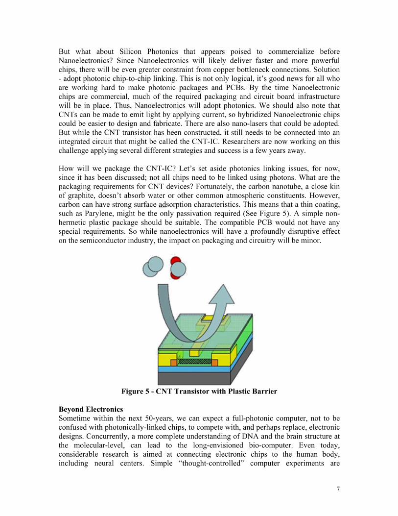
But what about Silicon Photonics that appears poised to commercialize before Nanoelectronics? Since Nanoelectronics will likely deliver faster and more powerful chips, there will be even greater constraint from copper bottleneck connections. Solution - adopt photonic chip-to-chip linking. This is not only logical, it’s good news for all who are working hard to make photonic packages and PCBs. By the time Nanoelectronic chips are commercial, much of the required packaging and circuit board infrastructure will be in place. Thus, Nanoelectronics will adopt photonics. We should also note that CNTs can be made to emit light by applying current, so hybridized Nanoelectronic chips could be easier to design and fabricate. There are also nano-lasers that could be adopted. But while the CNT transistor has been constructed, it still needs to be connected into an integrated circuit that might be called the CNT-IC. Researchers are now working on this challenge applying several different strategies and success is a few years away. How will we package the CNT-IC? Let’s set aside photonics linking issues, for now, since it has been discussed; not all chips need to be linked using photons. What are the packaging requirements for CNT devices? Fortunately, the carbon nanotube, a close kin of graphite, doesn’t absorb water or other common atmospheric constituents. However, carbon can have strong surface adsorption characteristics. This means that a thin coating, such as Parylene, might be the only passivation required (See Figure 5). A simple non-hermetic plastic package should be suitable. The compatible PCB would not have any special requirements. So while nanoelectronics will have a profoundly disruptive effect on the semiconductor industry, the impact on packaging and circuitry will be minor.
Figure 5 - CNT Transistor with Plastic Barrier
Beyond Electronics Sometime within the next 50-years, we can expect a full-photonic computer, not to be confused with photonically-linked chips, to compete with, and perhaps replace, electronic designs. Concurrently, a more complete understanding of DNA and the brain structure at the molecular-level, can lead to the long-envisioned bio-computer. Even today, considerable research is aimed at connecting electronic chips to the human body, including neural centers. Simple “thought-controlled” computer experiments are
8
succeeding and advancing. But perhaps we’ll merge logic technology with humans to enter the age of bionic enhancement that began many years ago. While bionic beings have been the theme of fiction writers, and the dream of some scientists, brain enhancements may be on the horizon. But do we even need hardware? The ultimate personal technology may be DNA modification that enables the mind to perform most of the functions now provided by our wearable electronics. The choices come down to external hardware, implants, or genetic engineering. In the next 50-years, the bioengineering of humans could provide extreme memory enhancement, a boost in left-brain computational capability (like savants), and the ability to receive and send data by RF. Many life forms can sense external energy forces, including regions of the electromagnetic spectrum, well beyond the range of humans. For better or for worse, we will have the knowledge to re-engineer humanity. More than Just Electrons We tend to think of high tech as electronics only, but most products incorporate other technologies, especially mechanics and optics. Our favorite gadgets typically use all three. Even the cell phone combines these technologies in the form of video displays, cameras, flash lamps, sound systems, pedometers and digital input means. But what if we could combine them on a single chip? We don’t have to wait for the future - the concept is here today. Right! MEMS (Micro-electro-mechanical systems) combines clusters of technologies into a microchip. The optical version, MOEMS (add opto-), or call it optical MEMS, is a subset that adds light control and other optical features to electronics and mechanics. But while MEMS has been around for years, in simple forms like inkjet printer chips and air bag sensors, we’re just at the beginning of advanced MEMS. MEMS is ready to become as pervasive as the computer chip. MEMS retains electronic functionality but adds mechanics and just about every other science and technology to make it an extremely potent and versatile technology suite. Today, MEMS provides inertial sensors used for virtually all air bags, new anti-roll-over detectors, “lost signal” back-up for GPS, pedometers, earthquake detectors, missile guidance, game controllers, and hundreds of other products. Optical MEMS chips are used in large HDTVs and digital cinema projectors, as well as in small digital projectors. Someday, MOEMS will be used to direct Internet signals using mirror arrays. But in the future, MEMS chips will deal with much more than electrons and photons. Gases, liquids and even nano-particles will be moved, sensed, detected, analyzed, manipulated, modified, and utilized by advanced fluidic-MEMS chips. Medicine and biology will be big benefactors of the tiny technology. Chips will detect pathogens in real time, and also amplify and analyze DNA - in minutes. And further into the future, the fluidic MEMS technology will be used to evaluate body chemistry and dispense drugs that might be synthesized using MEMS Pharmacy-on-a-Chip technology. MEMS, and other not-just-electrons devices, will play a key role in future health care. But conventional advanced electronics will work in concert to enable home visits by doctors using telemedicine. While today’s fledgling telemedicine uses strap-on blood pressure sensors, and cumbersome monitors, the future version will use wearable, and in some cases, implanted MEMS devices linked to heath care providers via wireless telemetry. We will have automatic emergency responses where the center can diagnose the condition, and perhaps handle the problem remotely.

9
Fluidic-MEMS, and other advanced devices, will need highly specialized packages and circuit boards. While packaging and circuitry still challenge the brightest minds, today’s products are designed around the electron. We will need to go beyond “electron plumbing” to handle fluids, gases and solids. Packages will require fluidic connectors as well as optical pathways. Circuit boards will need to accommodate all of these. Of all the types of devices for the future, MEMS, not Nanoelectronics, will prove to offer the greatest challenges. So what will the package and PCB for advanced MEMS look like? We’ll need a host of different types of interconnects to deal with photons, electrons, radio waves, liquids, gasses, nano-materials, and more. Forget solder, since its light-opaque, and we’ll want reconnectable systems anyway. Figure 6 shows fluidic-MEMS devices with reconnectable fittings that allow interconnection to other devices and a special circuit board. But there are two important features to note. The device is the package and the PCB has layers to handle fluids. It will be possible to build the entire device and package within a fab using wafer-level techniques. The MEMS-enabling PCB, with fluidic channels, could be made with today’s plastic-shaping technology, or with ceramic multilayer circuit methods.
Figure 6 - Fluidic MEMS System (ET-Trends)
10
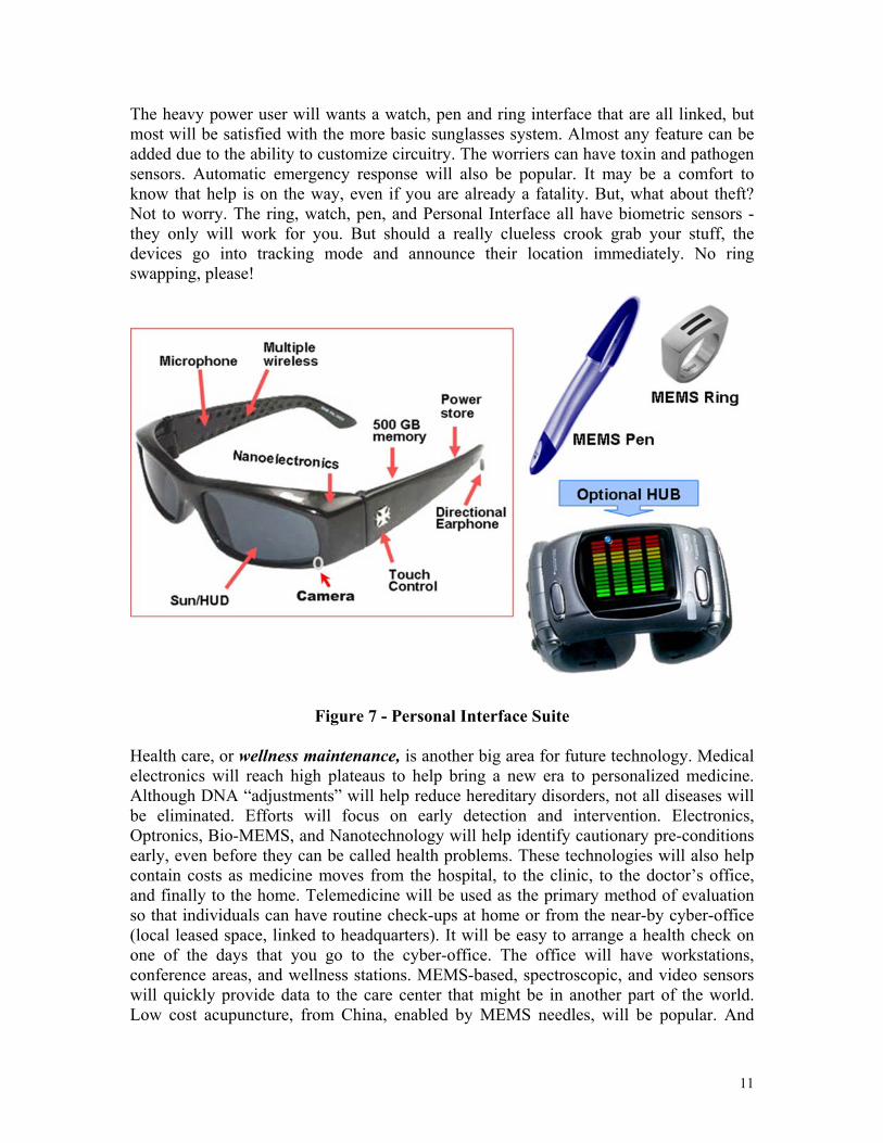
Future Products Now that we’ve explored many of the future building blocks of technology, what products can be constructed? Since we’ll continue to take on the grand challenges listed earlier, expect telecom personal products to be much more compact, loaded with features, highly efficient, and truly friendly. During the next 50 years, the smart phone that replaced the cell phone will evolve into a completely wearable Personal Interface (PI) product set. The Personal Interface will adopt form factors from today, such as sunglasses, watch/bracelets, pens, and rings. The user can settle for only the eyeglasses-style product. But a “power user” or gadget freak, who needs extra memory and unlimited functions, may decide to add a watch-like companion device. But the PI, looking like real cool sunglasses, can be a stand-alone product that provides the audio and video interface linked to a worldwide communications system. The PI will also link to other devices, such as the auxiliary watch and various input devices. The system will always be in contact with the Internet, accessed from anywhere, by any of several wireless linking systems. The video output will be a color stereo heads-up display (HUD) with picture quality as good as the View Master from the 1940’s. A 3D picture is easily achieved since each of the two micro-displays can be fed a slightly different picture that the eyes perceive as depth. Sound can be provided by MEMS-based ear speakers that generate high-quality stereo. Some may elect to have audio implants. The tiny chips within the eyeglass frames include a powerful CPU, considerable memory, audio, video, a multi-band transceiver, dual cameras that capture and send 3D images, and a power supply. Options include health monitors, such as pulse, blood pressure, and non-invasive analysis of glucose level, and almost anything, that is critical to the specific individual. Some will opt for night vision, but “see-through-fabric” terahertz viewers will be banned. The PI will let you visit with anyone around the world, tune in programs, attend conferences, retrieve data, run computations, pull up instruction manuals/diagrams, view maps while still seeing surroundings, and get help in an emergency. The extremely thin chips, now made of organic materials, will be curved to fit the contours of the frames. Most future circuitry will be flexible, but thinner and denser than today’s products. But the circuitry can also be incorporated into the housing, in this case, the sunglass frame. Nano inkjet technology will allow a complex circuit to be created on curved surfaces in milliseconds. Customized circuitry will be possible, with built-to-order products, like today’s Harley. So far, so good, but how about input? Where’s the mouse, or do we still need one? Fortunately, there are several choices. Many will opt for a MEMS gyroscopic pen that is RF-linked to the PI. Just write the text, or click on a display icon, and the gyroscope will instantly sense the movement that is then transmitted to the PI. Some will feel uncomfortable writing in the air with a pen. They can use a MEMS-enabled ring that also serves as the credit transaction interface. Move your finger, or hand, and a pointer moves on the display while a quick downward “mouse click” motion completes the action. Musicians can enjoy composing music, but dual rings are recommended. Voice commands will be 99.95% reliable and will be a popular input method. While considerable progress will be made in direct mind control, not everyone is comfortable with the technology.
11
The heavy power user will wants a watch, pen and ring interface that are all linked, but most will be satisfied with the more basic sunglasses system. Almost any feature can be added due to the ability to customize circuitry. The worriers can have toxin and pathogen sensors. Automatic emergency response will also be popular. It may be a comfort to know that help is on the way, even if you are already a fatality. But, what about theft? Not to worry. The ring, watch, pen, and Personal Interface all have biometric sensors - they only will work for you. But should a really clueless crook grab your stuff, the devices go into tracking mode and announce their location immediately. No ring swapping, please!
Figure 7 - Personal Interface Suite
Health care, or wellness maintenance, is another big area for future technology. Medical electronics will reach high plateaus to help bring a new era to personalized medicine. Although DNA “adjustments” will help reduce hereditary disorders, not all diseases will be eliminated. Efforts will focus on early detection and intervention. Electronics, Optronics, Bio-MEMS, and Nanotechnology will help identify cautionary pre-conditions early, even before they can be called health problems. These technologies will also help contain costs as medicine moves from the hospital, to the clinic, to the doctor’s office, and finally to the home. Telemedicine will be used as the primary method of evaluation so that individuals can have routine check-ups at home or from the near-by cyber-office (local leased space, linked to headquarters). It will be easy to arrange a health check on one of the days that you go to the cyber-office. The office will have workstations, conference areas, and wellness stations. MEMS-based, spectroscopic, and video sensors will quickly provide data to the care center that might be in another part of the world. Low cost acupuncture, from China, enabled by MEMS needles, will be popular. And
12
those who need next-stage-treatment can visit a clinic for additional assistance where tiny sensors, and agents might be implanted. But, within the next 50-years, implants will be able to analyze and treat, with drugs and other means. There will also be wellness agents that can be injected by syringe. A mobile MEMS device team may “swim” through your circulatory system and routinely remove plaque, growths, or anything that could develop into a problem. The mobile MEMS devices will use lasers, mechanical surgical tools, and drugs. In the future, doctors will make house calls without leaving the medical center. And health care micro- and nano-agents will work tirelessly - internally and invisibly, generating self-sustaining energy from body chemistry. Conclusions We have reached a point of no return for technology. The future world cannot exist without technology and would catastrophically collapse. But, technology must continue to advance to keep pace with problems - some of which are created by technology itself. Hopefully, technology will surpass the mass of problem, both old and new, when mankind decides to stop being more of the problem than the solution. Electronics will continue to play an important role, but will share the high tech stage with many other disciplines, especially micromechanics, photonics, nanotechnology, and others. The convergence of the sciences will continue to happen at the device level to bring about unimagined new products. The future will be exciting but some will mourn the loss of favorite technologies. Copper will be replaced by organic molecules, solder will make way for reconnectable technologies, including Lego-like structures and micro-Velcro, and circuit boards will no longer be etched. For those who embraced emerging technology for the past 50-years, get ready - the next 50 will really be something. And thanks to medical advancements, we might all be here to watch it unfold. Finally, to those who are new to the tech game, you are in for a thrilling half-century of progress, but don’t just be a spectator. References [1] Hanson, A., British Patent 4,681, 1903. [2] Gilleo, K., "First 7000 Years of Soldering - Part 1 - Metallurgy", Circuits Assembly,
pp. 30-34, October 1994. [3] Gilleo, K., "First 7000 Years of Soldering - Part II- Polymers", Circuits Assembly, pp.
44 - 45, November 1994. [4] Gilleo, K., “The 7,000 Year Cycle”, Circuits Assembly, Vol. 16, June 2005.
[This chapter will appear in the IPC’s 50th Anniversary Book due out in 2007]