the hb-75 transceiver
TRANSCRIPT

The HB-75 Transceiver
Mike Bohn, KG7TR
December, 2020
Introduction
Construction of the HB-75 Transceiver shown in Figure 1 was prompted by acquisition of a
mechanical filter and a LMB Heeger cabinet and chassis. This radio is a great performer. The
filter is a 455 KHz lower sideband (LSB) unit, manufactured in the 1960s by a Japanese
company called Kokusai. As far as I am able to determine, Kokusai filters were available from
Lafayette Radio with their markings, and were used in some of their receivers. They were also
used in some KW series radios built in the UK, and possibly some Japanese equipment.
Figure 1: The HB-75 Transceiver
The LMB Heeger cabinet is roughly styled and sized to match a Collins KWM-2 transceiver
or a 30L-1 linear amplifier. These cabinets and matching chassis are still available, but are not
cheap. I toyed with the idea of using all octal tubes and possibly a multi-band configuraton. But
with the number of circuits required, physical size constraints, and limited selection of dual
section octal tubes, I decided to go with a single band radio using 7 and 9 pin miniature tubes.
This pretty much filled up all the available “real estate” on the chassis.
The LSB filter was designed for a carrier frequency of exactly 455.0 KHz. Kokusai also
made a matching USB filter for the same carrier frequency. Using the LSB filter allowed
construction of a single conversion radio for 75 meters, using a variable frequency oscillator
(VFO) frequency 455 KHz below the desired LSB signal output. Due to some practical VFO
limitations explained later, the radio covers 3.8 to 4.0 MHz. This is the current phone allocation
for General class licenses (although I have an Extra), and the vintage radio nets I participate in
are all in this range.
Power for the radio comes from an external Heathkit HP-23B supply. Because this supply’s
filament voltage is 12.6 VAC, various heaters in the radio are connected in series and parallel
arrangements. Some of this also resulted from my supply of tubes. I have a ton of 6BA6s, and
only a few 12BA6s. The Heathkit supply was also modified to provide 12 VDC to power the
various relays, the digital display, and a 6 VDC regulator in the radio for the VFO’s filament. I
was able to squeeze a transformer and other necessary parts under the HP-23B chassis.
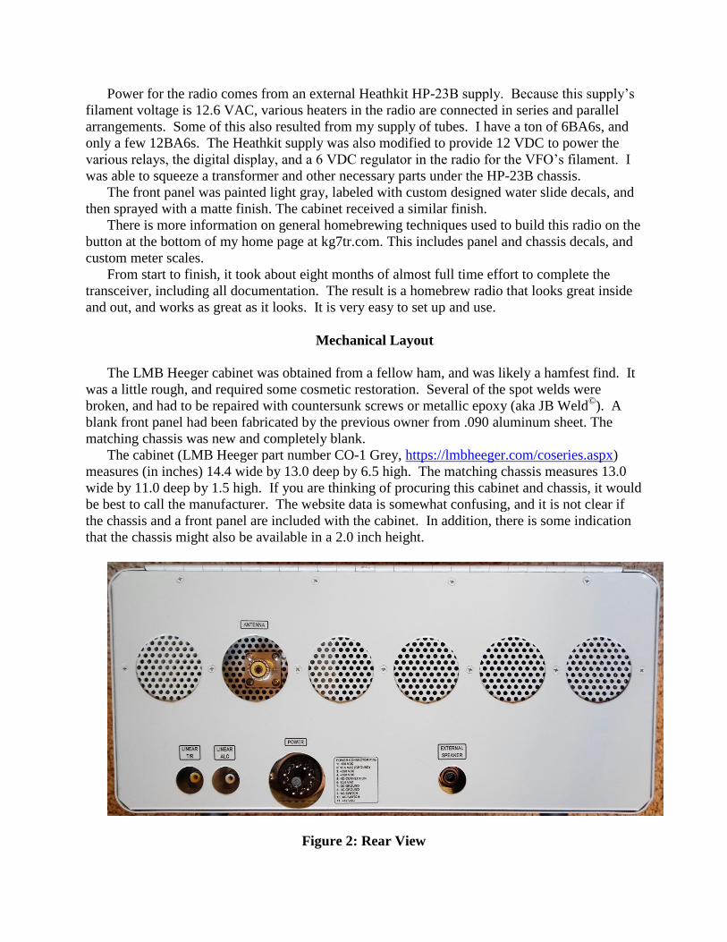
The front panel was painted light gray, labeled with custom designed water slide decals, and
then sprayed with a matte finish. The cabinet received a similar finish.
There is more information on general homebrewing techniques used to build this radio on the
button at the bottom of my home page at kg7tr.com. This includes panel and chassis decals, and
custom meter scales.
From start to finish, it took about eight months of almost full time effort to complete the
transceiver, including all documentation. The result is a homebrew radio that looks great inside
and out, and works as great as it looks. It is very easy to set up and use.
Mechanical Layout
The LMB Heeger cabinet was obtained from a fellow ham, and was likely a hamfest find. It
was a little rough, and required some cosmetic restoration. Several of the spot welds were
broken, and had to be repaired with countersunk screws or metallic epoxy (aka JB Weld©
). A
blank front panel had been fabricated by the previous owner from .090 aluminum sheet. The
matching chassis was new and completely blank.
The cabinet (LMB Heeger part number CO-1 Grey, https://lmbheeger.com/coseries.aspx)
measures (in inches) 14.4 wide by 13.0 deep by 6.5 high. The matching chassis measures 13.0
wide by 11.0 deep by 1.5 high. If you are thinking of procuring this cabinet and chassis, it would
be best to call the manufacturer. The website data is somewhat confusing, and it is not clear if
the chassis and a front panel are included with the cabinet. In addition, there is some indication
that the chassis might also be available in a 2.0 inch height.
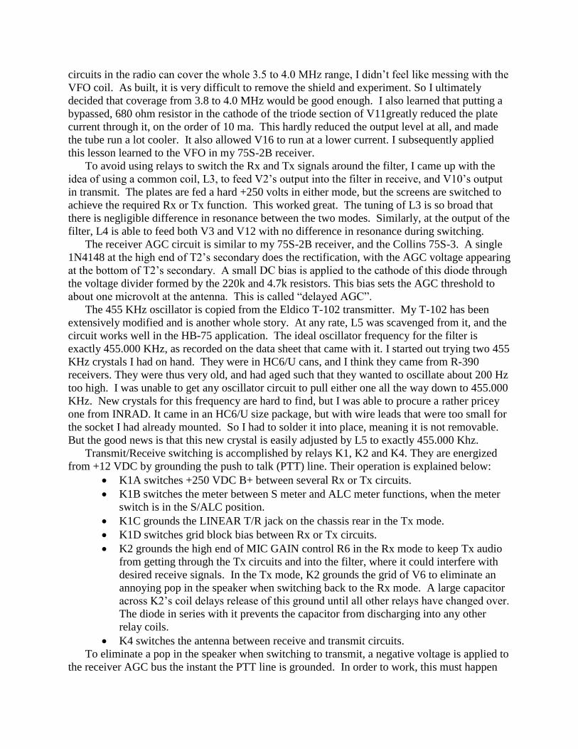
Figure 2: Rear View

I think the chassis really should have been about one inch deeper, i.e., 12 inches deep instead
of 11. Ideally, you want the chassis to butt up against the back of the cabinet so that rear panel
connectors can protrude enough for mate and demate action. However, with the 11 inch depth,
positioning the chassis against the back of the cabinet left way too much overhang over the front
panel. Note that there are no suitable chassis sizes available from Hammond or Bud that will
work in this cabinet.
As it was, I ended up with a compromise position with a one inch gap between the chassis
rear and the cabinet back. Large holes were punched in the cabinet back to allow my fingers to
grip mating connectors. I also punched several 1.75 inch holes in the cabinet rear to provide
more ventilation, and covered these with perforated aluminum sheet. The recessed connectors
are visible in Figure 2, which shows the cabinet rear with the chassis installed.
Figure 3: Transceiver Top View

Figure 4: Transceiver Bottom View
Figures 3 and 4 show the chassis top and bottom respectively. The cabinet as supplied new
comes with side rails for sliding in the chassis. One of these was missing on my cabinet, so I
fabricated new rails out of .062 inch angle stock. The chassis is mounted in the cabinet by four 6-
32 screws that thread into PEM type nuts pressed into in the chassis corners.
The chassis is made from .050 inch soft aluminum, which is not sturdy enough for a SSB
radio that requires a mechanically stable analog VFO. So a sheet of .062 tempered aluminum
was added under the VFO components as can be seen in Figure 3. The VFO coil is mounted to
this plate inside a shield made from .062 perforated sheet and angle stock. The power amplifier
(PA) components at the rear are housed in a 5 inch cube made the same way. It is shown in
Figure 5. To further beef up things topside, angle brackets run from the front panel to the chassis
to prevent flexing.

Figure 5: Interior of PA Cage
To finish off the mechanical assembly, an array of shields is mounted underneath the chassis,
as can be seen in Figure 4. These are made from .062 tempered sheet and .5 inch angle stock.
Some are fastened to a strip of .5 inch angle stock that runs across the chassis width at about the
centerline. The end result of all these mechanical features is a radio that is quite stout. There is
almost no change in VFO frequency when the cabinet is moved around.
Block Diagram Circuit Description
The block diagram of the transceiver is shown in Figure 6. Similar to my Octal Tribander
transceiver, the HB-75 uses independent tuned circuits for the receiver front end and the
transmitter driver, instead of sharing them as was typical in a lot of the old commercial

transceivers. It takes a few additional parts and requires an extra tuning control, but I find it less
trouble to do it this way. Starting at the lower left of the diagram, the antenna jack is connected
to a T/R relay. In the receive (Rx) mode the antenna is routed to an input LC circuit that feeds
the grid of RF amplifier V1. The output of V1 is run through another LC circuit and then on to
mixer V2. The LC circuits are tuned by a dual section variable capacitor brought out to the front
panel as the Rx PRESELECTOR control.
Figure 6: Transceiver Block Diagram
V2 is a pentagrid mixer that, in the receive mode, combines the amplified RF from V1 with a
VFO injection voltage from V11B. The injection frequency is 3.345 to 3.545 MHz. When
subtracted from the incoming signal of 3.8 to 4.0 MHz, a .455 MHz LSB intermediate frequency
(IF) signal results. The 455 KHz signal at the plate of V2 is applied to the mechanical filter
through a matching transformer. The primary of this transformer is also connected to the plate of
transmit (Tx) isolation amplifier V10, which applies a double sideband (DSB) signal to the filter
in the transmit mode.
The output of the mechanical filter is applied, through another matching transformer, to the
grid of V3 and the deflection plates of V12. V3 functions as an IF amplifier for the receive mode,
while V12 functions as a mixer for the transmit mode. The output of V3 is fed to V4, an IF
amplifier whose output goes to V5, the product detector and audio amplifier. The output of V4
is also rectified to generate the Rx AGC voltage. This voltage is fed to V1, V3 and V4, and

holds the audio output level virtually constant once a threshold of approximately a microvolt of
RF at the antenna is exceeded. Negative bias from the IF GAIN control is added to the AGC
voltage to control overall gain.
V5A (triode section) serves as a product detector, with 455 KHz LSB IF signal applied to its
grid and 455 KHz BFO fed to its cathode. Audio is recovered and filtered at the plate, and then
coupled to the AF gain control. From here it goes to the grid of V5B (pentode section), where it
is amplified and fed to V6, the audio output amplifier. Output of this stage is transformer
coupled to the internal speaker. The output can also be connected to external headphones or an
external speaker.
For the transmit mode, audio from the microphone is amplified by V7A (pentode section),
and then applied to the mic gain control through normally closed (NC) relay contacts when the
front panel function switch is in the in the PTT or MOX position. When this switch is in the
TUNE position, the relay is energized. This turns on V8 tone oscillator and applies its output to
the MIC GAIN control. The signal at the wiper of the MIC GAIN control is applied to the grid of
V7B (triode section), which is a cathode follower. Its low impedance output is coupled to the
diode balanced modulator.
V9 is a dual triode that generates a 455 KHz crystal controlled signal used for Rx BFO and
Tx carrier functions. V9A is the crystal oscillator, with its output applied to V9B, a
buffer/amplifier that provides a low impedance output signal for the balanced modulator and
product detector circuits.
V11A (pentode section) serves as a stable Colpitts oscillator whose output varies from 3.345
to 3.545 MHz. Output from the cathode of the pentode section is coupled to the grid of V11B
(triode section), which is a cathode follower. Output of this follower is coupled to V2 and V12.
V16 provides regulated B+ voltage to both sections of V11. In addition, regulated 6 VDC is
applied to the filaments of this tube from an onboard regulator. This VFO has exceptional
overall stability.
The balanced modulator is a ring diode type using four silicon diodes. Its double sideband
output, absent the carrier, is transformer coupled to the grid of isolation amplifier V10. The
output of V10 is coupled to the input of the mechanical filter through the same transformer used
by V2 (the plates of these two tubes are connected together). In Tx mode the filter removes the
unwanted upper sideband from the balanced modulator DSB signal, leaving only a LSB signal at
its output.
V12 is a balanced mixer for the transmit function. The 455 KHz LSB signal is applied to its
deflection plates, while the VFO signal is applied to its signal grid. The balancing action of this
tube combined with the output LC circuit eliminate all unwanted signals (in particular the VFO
signal), such that only the desired 3.8 to 4.0 MHz LSB signal remains. This is coupled to the
grid of V13, where it is amplified to a level suitable for driving the PA grids. The output of V13
is also filtered by a LC circuit and coupled into the grids of V14 and V15. The LC circuits at the
input and output of V13 are tuned by a dual section variable capacitor brought out to the front
panel as the Tx DRIVER control.
PA tubes V14 and V15 are connected in parallel and amplify the SSB signal from the driver
to 100 watts PEP. Their output is coupled through a pi network to the antenna through contacts
on the T/R relay. The pi network is tuned by variable capacitors brought out to the front panel as
the PA TUNE and PA LOAD controls.
If the PA tubes are over driven such that grid current flows, this signal is rectified to produce
a negative ALC voltage that is applied to the grid of V10. The negative voltage reduces the gain

of V10 to help prevent over drive conditions. A rear panel connector also allows ALC from a
linear amplifier to be applied to V10.
A small pickup wire is mounted next to the VFO coil. This signal is sent to the digital
frequency counter/readout, where a programmed 455 KHz IF offset produces the correct output
frequency display.
Transmit/Receive changeover is provided by three internal relays that primarily switch B+,
grid block bias and the antenna between Rx and Tx circuits. Other relay switching is used to
mute Rx or Tx audio, switch the meter between modes, and key an external linear amplifier. As
mentioned previously, the plates of V2 and V10 are connected together and fed through a
common transformer primary. The secondary of this transformer feeds the input of the
mechanical filter. Constant B+ is applied to the plates of these tubes, but their screen voltages
are switched between the Rx/Tx modes. Without screen voltage, the affected tube is effectively
turned off.
Additional Circuit and Construction Notes
A full schematic diagram of the HB-75 is available on the respective page at kg7tr.com, and
should be referred to in this discussion. This information supplements the basic circuit
descriptions provided in the previous section.
The only RF inductors I elected to label as transformers are T1 and T2. These are KTran
type IF transformers with tuned primary and secondary coils. The rest of the RF coils are labeled
with “L” reference designators, even if they have two coupled windings (e.g., L1, L3, L4, L7 and
L10). For these, only one winding is resonated, so I called them coils.
The dual section variables for the Rx RF amplifier and the Tx driver have 100 pf “padder”
capacitors in series. This was done to increase the bandspread range of the variables, such that it
is not possible to accidently tune them to the VFO frequency.
When bread boarding some of the 455 KHz circuits, I was unable to make usable, high-Q
inductors using toroid coils. So I had to go to my junk box of slug tuned coils and old IF
transformers, and cobble together suitable parts. And it seems that such vintage inductors and IF
transformers are not readily available on the internet, or are ridiculously priced when they are.
Maybe there are ferrite or powdered iron toroid or pot cores that would yield Qs similar to the
vintage slug tuned coils with their universal windings and Litz wire. But I didn’t really see
anything in Amidon’s data sheets. As it turned out, the only toroids used are L3 and L4 at the
input and output of the filter. These are wound on FT-43A forms. They are essentially
impedance matching transformers. Their Q is not great, but selectivity is not important here, and
there is ample gain in the receiver and transmitter paths such that they work just fine. Most of
the coil cans came from junked TVs that my dad used to have in the basement. .75 inch square
holes were punched in the chassis to mount them. Some required fastening spring clips to their
sides so they could be snapped to the chassis. For the KTran units, I made a drill template for
their complex footprint. My digital inductance meter was indispensable for finding the right coils
in the junk box to make this radio. And at the end of the day, using slug tuned coils helped make
the experimentation and alignment go smoothly.
Like most of my homebrew radios, the VFO components were from an old ARC-5
transmitter. As it turned out, the ARC-5 coil I used has about 4 µH of inductance, and only
produced a useful bandspread of about 250 KHz within the required range using the matching
ARC-5 variable capacitor. In order to increase the bandspread, I would have had to reduce its
inductance by removing turns or tapping down on its winding. Although the rest of the tuned
circuits in the radio can cover the whole 3.5 to 4.0 MHz range, I didn’t feel like messing with the
VFO coil. As built, it is very difficult to remove the shield and experiment. So I ultimately
decided that coverage from 3.8 to 4.0 MHz would be good enough. I also learned that putting a
bypassed, 680 ohm resistor in the cathode of the triode section of V11greatly reduced the plate
current through it, on the order of 10 ma. This hardly reduced the output level at all, and made
the tube run a lot cooler. It also allowed V16 to run at a lower current. I subsequently applied
this lesson learned to the VFO in my 75S-2B receiver.
To avoid using relays to switch the Rx and Tx signals around the filter, I came up with the
idea of using a common coil, L3, to feed V2’s output into the filter in receive, and V10’s output
in transmit. The plates are fed a hard +250 volts in either mode, but the screens are switched to
achieve the required Rx or Tx function. This worked great. The tuning of L3 is so broad that
there is negligible difference in resonance between the two modes. Similarly, at the output of the
filter, L4 is able to feed both V3 and V12 with no difference in resonance during switching.
The receiver AGC circuit is similar to my 75S-2B receiver, and the Collins 75S-3. A single
1N4148 at the high end of T2’s secondary does the rectification, with the AGC voltage appearing
at the bottom of T2’s secondary. A small DC bias is applied to the cathode of this diode through
the voltage divider formed by the 220k and 4.7k resistors. This bias sets the AGC threshold to
about one microvolt at the antenna. This is called “delayed AGC”.
The 455 KHz oscillator is copied from the Eldico T-102 transmitter. My T-102 has been
extensively modified and is another whole story. At any rate, L5 was scavenged from it, and the
circuit works well in the HB-75 application. The ideal oscillator frequency for the filter is
exactly 455.000 KHz, as recorded on the data sheet that came with it. I started out trying two 455
KHz crystals I had on hand. They were in HC6/U cans, and I think they came from R-390
receivers. They were thus very old, and had aged such that they wanted to oscillate about 200 Hz
too high. I was unable to get any oscillator circuit to pull either one all the way down to 455.000
KHz. New crystals for this frequency are hard to find, but I was able to procure a rather pricey
one from INRAD. It came in an HC6/U size package, but with wire leads that were too small for
the socket I had already mounted. So I had to solder it into place, meaning it is not removable.
But the good news is that this new crystal is easily adjusted by L5 to exactly 455.000 Khz.
Transmit/Receive switching is accomplished by relays K1, K2 and K4. They are energized
from +12 VDC by grounding the push to talk (PTT) line. Their operation is explained below:
K1A switches +250 VDC B+ between several Rx or Tx circuits.
K1B switches the meter between S meter and ALC meter functions, when the meter
switch is in the S/ALC position.
K1C grounds the LINEAR T/R jack on the chassis rear in the Tx mode.
K1D switches grid block bias between Rx or Tx circuits.
K2 grounds the high end of MIC GAIN control R6 in the Rx mode to keep Tx audio
from getting through the Tx circuits and into the filter, where it could interfere with
desired receive signals. In the Tx mode, K2 grounds the grid of V6 to eliminate an
annoying pop in the speaker when switching back to the Rx mode. A large capacitor
across K2’s coil delays release of this ground until all other relays have changed over.
The diode in series with it prevents the capacitor from discharging into any other
relay coils.
K4 switches the antenna between receive and transmit circuits.
To eliminate a pop in the speaker when switching to transmit, a negative voltage is applied to
the receiver AGC bus the instant the PTT line is grounded. In order to work, this must happen
before any relays change state. It is accomplished by the .47 µf capacitor and two diodes
connected to the PTT line. In Rx, the capacitor charges up to about 11 volts because one end is
connected to +12 VDC and the other end is grounded through the diode whose cathode is
connected to ground. As soon as the PTT line is grounded, the left end of this capacitor becomes
negative with respect to ground. This voltage is applied to the AGC line through the other diode,
and effectively mutes the receiver instantly.
Relay K3 is energized when the TUNE function is selected. One set of contacts grounds the
cathode circuit of tone oscillator V8, turning it on. The other set switches the input to MIC
GAIN R6 from the output of V7A to the output of V8. A voltage divider (24k and 36k resistors)
in the plate circuit of V8 reduces the audio voltage to an equivalent microphone level for tune up.
The balanced modulator is a standard circuit used in several of my homebrew radios, as well
as many commercial rigs. Trimmer C7 is mounted on the side of the chassis next to L10. It was
added later (after the new crystal was installed), and is not shown in Figure 4. Adjusting C7 and
R7 provides carrier suppression greater than 50 dB. L10 was a junk box find, and tunes very
broadly. I think it might have been an oscillator coil from an old broadcast band radio. The slug
or the value of the resonating 620 pf capacitor do not have a whole lot of effect. I mainly needed
a coil like this to simultaneously couple both the output of the balanced modulator and ALC
voltage into the grid of V10.
The V12 Tx balanced mixer circuit was cloned from various circuits found in the ARRL
handbooks. It provides good conversion gain, and effectively nulls out the VFO signal from its
output. I have come to the conclusion that the secret to balanced modulators and balanced
mixers lies in the output LC tank circuit. Diode circuits are low impedance, and seem to work
best with low L/C ratios, whereas tube circuits are high impedance, and need high L/C ratios
with bifilar windings. L7 was another junk box find, and had a bifilar winding. It may have
been from a television set’s 4.5 MHz sound IF ratio detector. I added a secondary winding to
couple to V13, with a 22 pf parallel capacitor across it that allowed resonance with C3A.
Because of layout constraints, L7 had to be located a few inches from the plates of V12. So a
twisted pair of wires was used to make the connections, and this works just fine. One thing I did
notice is that, just as RCA advises, V12 is indeed very sensitive to magnetic fields around it.
Using a metal screwdriver to adjust R5 causes the balance to shift when the screwdriver is
removed. This is very apparent if the screwdriver happens to have a magnetic tip!
The ALC circuit is the same as my other homebrew transmitters, and is copied from the
Heathkit SB series of radios. As the PA grids begin to draw current due to being overdriven,
these current pulses are rectified and generate a negative ALC voltage that reduces the gain of
V10.
Turning to the metering circuit, in the PLATE position of the METER switch the meter
measures the voltage at the cathodes of the PA tubes, which are connected to ground through a
one ohm shunt resistor. Thus, a cathode current of 250 ma will produce 250 mv of voltage
across the resistor. This voltage is scaled to the meter sensitivity by the 4.7k resistor in series
with it.
In the S/ALC position of the METER switch, there are two voltages to measure. In the Rx
mode, the voltage at the cathode of V3 decreases as signal strength and AGC voltage increase.
In the Tx mode, the voltage at the cathode of V10 decreases as ALC voltage increases. Relay
contacts at K1B switch the appropriate voltage into the meter circuit. The voltages are compared
by the meter to a fixed reference voltage set by R4. In the Rx mode, this pot sets the reference
voltage equal to the zero signal voltage at the cathode of V3, so that the meter reads zero. This

setting is unchanged for the Tx mode. In Tx, R3 is used to set the zero signal voltage at the
cathode of V10 to equal that already set by R4. With this configuration, only a single set of relay
contacts is required to switch between Rx and Tx metering. The 9.1k resistor in the circuit sets
the sensitivity of the S meter so that S9 occurs at half scale deflection. The diode and 270 ohm
resistor provide compression at the higher readings so that the meter can read up to +40 dB over
S9 without pegging past full scale. The ALC meter has no specific calibration. Its main purpose
is to show when V10 is being hit with ALC voltage.
The driver and PA circuits are conventional, and very similar to my other radios. PA NEUT
capacitor C6 provides out of phase feedback to neutralize the PA grid to plate capacitance. It is
adjusted so that plate current dip and maximum power output occur at the same setting of C4,
when tuned into a dummy load.
The filaments are wired in series and parallel arrangements as required to work from a 12.6
VAC source. V12 and V13 have non-standard filament currents (350 ma and 650 ma
respectively), so it was necessary to connect V10 and V12 filaments in parallel to make it all
work out.
K2 and K3 are small signal relays with special alloy contacts for switching low level signals.
They are contained in 16 pin DIP packages. These packages are plugged into sockets on a
prototype circuit board so they can be changed if required. The proto board also allowed
mounting a lot of other miscellaneous parts and connections that would have been difficult to
wire up on terminal strips. I called the whole thing a relay module, which is seen towards the
chassis rear in Figure 4. The schematic of all these circuits is shown on sheet 3 of the schematic
diagram.