the role of point defects in pbs, pbse and pbte: a first
TRANSCRIPT

1 © 2015 IOP Publishing Ltd Printed in the UK
1. Introduction
Lead chalcogenides (PbX, X = S, Se and Te), a family of narrow band gap IV–VI semiconductors, have been the sub-ject of intensive research due to their applications in many fields such as thermoelectric energy converters [1, 2], thermal photovoltaic devices [3], infrared lasers [4] and light- emitting diodes [5]. Together with the CdX chalcogenides family (CdS, CdSe, CdTe), the PbX systems are abundantly used in heterogeneous nanocrystals (HNCs) to create new materials with novel and tunable physical properties [6–8].
By physical nature, defects inevitably exist in crystals, and play a pivoting role in their growth and synthesis, and in many physical properties of HNCs and multicomponent quantum
dots (QDs). First, point defects, depending on the position of their defect states with respect to the band gap, can deter-mine whether the process of the electron–hole recombination in nanocrystals is radiative or non-radiative [9, 10]. Thus, point defects directly affect the quantum yield of nanocrystal (NC) QDs. Second, there is much unclarity in the literature about how the off-stoichiometry of the NCs [11, 12], a typ-ical product of wet chemical synthesis, affects the physical properties. In particular, it is at present unclear whether the excess or depletion of anions or cations is accommodated only at the surface, or also at the interior of the NCs. Third, the very important cation exchange (CE) process that is used to create core-shell type structures and the synthesis of NCs in deviating crystal structures [7, 13–20], requires the migration
Journal of Physics: Condensed Matter
The role of point defects in PbS, PbSe and PbTe: a first principles study
Wun-Fan Li, Chang-Ming Fang, Marjolein Dijkstra and Marijn A van Huis
Soft Condensed Matter, Debye Institute for Nanomaterials Science, Utrecht University, Princetonplein 5, 3584CC Utrecht, The Netherlands
E-mail: [email protected]
Received 30 April 2015, revised 3 July 2015Accepted for publication 6 July 2015Published 17 August 2015
AbstractIntrinsic defects are of central importance to many physical and chemical processes taking place in compound nanomaterials, such as photoluminescence, accommodation of off-stoichiometry and cation exchange. Here, the role of intrinsic defects in the above mentioned processes inside rock salt (RS) lead chalcogenide systems PbS, PbSe and PbTe (PbX) was studied systematically using first principles density functional theory. Vacancy, interstitial, Schottky and Frenkel defects were considered. Rock salt PbO was included for comparison. The studied physical properties include defect formation energy, local geometry relaxation, Bader charge analysis, and electronic structure. The defect formation energies show that monovacancy defects and Schottky defects are favoured over interstitial and Frenkel defects. Schottky dimers, where the cation vacancy and anion vacancy are adjacent to each other, have the lowest defect formation energies at 1.27 eV, 1.29 eV and 1.21 eV for PbS, PbSe and PbTe, respectively. Our results predict that a Pb monovacancy gives rise to a shallow acceptor state, while an X vacancy generates a deep donor state, and Schottky defects create donor-acceptor pairs inside the band gap. The surprisingly low formation energy of Schottky dimers suggests that they may play an important role in cation exchange processes, in contrast to the current notion that only single point defects migrate during cation exchange.
Keywords: density functional theory, lead chalcogenides, point defect, defect state, photoluminescence, off-stoichiometry, cation exchange
S Online supplementary data available from stacks.iop.org/JPhysCM/27/355801/mmedia
(Some figures may appear in colour only in the online journal)
W-F Li et al
The role of point defects in PbS, PbSe and PbTe: a first principles study
Printed in the UK
355801
JCOMEL
© 2015 IOP Publishing Ltd
2015
27
J. Phys.: Condens. Matter
CM
0953-8984
10.1088/0953-8984/27/35/355801
Papers
35
Journal of Physics: Condensed Matter
JW
0953-8984/15/355801+14$33.00
doi:10.1088/0953-8984/27/35/355801J. Phys.: Condens. Matter 27 (2015) 355801 (14pp)

W-F Li et al
2
of cations, as shown in many experimental studies. In RS chal-cogenides, this is assumed to be mediated by cation vacancies [7, 20]. Groeneveld et al proposed that ZnSe–CdSe colloidal quantum dots (QD) can be tailored via a CE mechanism medi-ated by Frenkel pairs of Zn interstitials Zn i and Zn vacancies VZn [18]. Marianna et al proposed a plausible mechanism that the growth of PbSe/CdSe core/shell nanocrystal is formed by CE, where the cation vacancies assist the migration of cations [7]. Yingzhuo et al proposed that CdSe/ZnSe core/shell QD can be synthesised in an aqueous environment through CE [19]. Finally, Yalcin et al recently found that the CE in the solid-solid-vapour (SSV) growth of PbSe/CdSe core/shell HNCs is mediated by Cd vacancies at the PbSe-CdSe interface [20]. However, it is difficult, or even impossible to determine experimentally which types of defects are present in the mate-rial and what their role is in, e.g. CE progresses. It was only until recently that more insight into CE was unveiled by first principles calculations of Ag ions in wurtzite CdSe [21]. To the best of our knowledge, our current work is the first DFT study discussing point defects in RS PbX in the context of the CE process. Although in all the experimental literature given above monovacancies are presumed to enable CE, we give an important finding that vacancy comlexes, i.e. Schottky defects, cannot be excluded in CE because they possess significantly lower formation energies than monovacancies do. In all these phenomena, the presence of vacancies and other point defects is a crucial parameter. In this work, we identify and charac-terise the most important point defects in PbX chalcogenides, and discuss their role in the above mentioned processes.
In the current study, four kinds of point defects are con-sidered. These are vacancy, interstitial, Schottky dimer/pair and Frenkel pairs. These defects are schematically shown in figure 1. Vacancies and interstitials contain only one defect site, while Schottky and Frenkel defects include two defect sites. A Schottky defect consists of a cation-anion vacancy pair. A Schottky dimer is defined as the cation vacancy and the anion vacancy sites being adjacent to each other, and in the Schottky pair configuration, the two defect sites are sepa-rated as far as possible within a supercell. A Frenkel defect is created when an atom moves from its original place to an interstitial site, whereby a vacancy site and an interstitial site are generated. In binary compounds such as PbX, both the cation Frenkel defect and the anion Frenkel defect need to be considered.
Defects in PbX have received much attention from scien-tists for decades. The related research has been carried out both experimentally [22–27] and theoretically [23, 28–38]. Miller et al found that the formation energy of a Frenkel defect is higher than a Schottky defect in PbTe, hence the diffusion is essentially controlled by a vacancy-type mecha-nism [22]. By using a positron annihilation technique, Polity et al established the relationship between VPb concentration and positron lifetime [23]. Yoneda et al reported that Schottky defects will form in PbTe when the crystal is heated over 200 °C [25]. Via the measurements of step-scan Fourier-transform infrared photoreflectance (step-scan FTIR PR) on a PbTe thin film, the defect state of VTe was found at 29.1 meV above the conduction band maximum (CBM), and another defect state
at 18.1 meV below the valence band maximum (VBM) may be attributed to VPb or threading dislocations, whereas no states were found in the band gap [26]. Koumoulis performed NMR measurements on PbSe, and reported a p-type shallow acceptor state and a n-type deep state at the midgap [27].
Theoretical calculations were also performed on PbX systems. Berashevic carried out a detailed study on vacancy defects in α-PbO (litharge structure) [36], and found the charged defect states for −VPb
2 at 0.1 eV below the VBM, and +VO at 1.03 eV above the VBM, which were stabilised by
charge transfer. For PbS, Ding et al studied the (1 0 0) sur-face, and found the p-type VPb and n-type VS defect states. They also found that the structural relaxation at the surface is opposite to the case of bulk PbS: around the defect site, the nearest–neighbouring (NN) atoms of the defect site will be repelled outwards, while the next-nearest–neighbouring (NNN) atoms will move toward the defect site [32]. Walsh studied vacancy defects and Schottky defects in their neutral and charged states [34]. The Schottky defect was found to be preferred over vacancy defects as it has a lower formation energy. Donghun et al found for PbS quantum dots (QD) that off-stoichiometry will introduce new states which are highly localised on certain surface atoms [38]. For PbSe, Peng et al performed a series of calculations for bulk PbSe doped with 26 substitutional impurities [35]. Wrasse et al studied the elec-tronic structure of both bulk and nanowire PbSe with group III substitutional impurities [37]. For PbTe, there are a series of theoretical studies concerning the defect states: Parada and Pratt made the first attempt to describe the electronic structure of defective PbTe using the Slater–Koster model, [28, 29] and Lent et al used a tight-binding method to give a qualitative description of the deep defect state in PbTe [30]. However, the calculations in [28–30] are non-self-consistent calcula-tions. Recently, Ahmad and Hoang employed self-consistent DFT calculations for vacancies and substitutional impurities in both bulk [31, 33] and thin-film [33] PbTe. Furthermore, there have been several other theoretical investigations done on perfect PbX systems for structural and electronic proper-ties [39–42], and thermodynamic properties [43–45]. All of these studies are limited to perfect PbX crystals, though, thus no defect was induced.
The formation energy of defects is key to verifying which kind of defect(s) are more likely to be formed inside a crystal, and thus may determine the CE process. Using the first principles DFT approach, we first aim to compare the relative stability of the defect species inside PbX in terms of defect formation energy, so that we can identify which defects may be involved in the CE process. Second, we would like to provide a fundamental and panoramic view of the physical properties of the point defects inside PbX, which is indispensible for further study and applications of these materials. Besides defect formation energies, the phys-ical properties including local geometry relaxation, charge transfer and electronic structure, were analysed. The typical point defects for these compounds are: vacancy, intersti-tial, Schottky and Frenkel. Even though PbO occurs in the litharge structure rather than the rock salt (RS) phase [46], we include the calculations of RS PbO for comparison.
J. Phys.: Condens. Matter 27 (2015) 355801

W-F Li et al
3
The content of this paper is organised as follows: the com-putational details are given in section 2. The results and dis-cussions are presented in sections 3 and 4, respectively; first we will compare the relative stability of all the defect types, after which we select the more stable ones for a more detailed study of physical properties. Finally, the conclusions are given in section 5.
2. Computational details
2.1. Computational settings
All the calculations were carried out using the first principles DFT code VASP [47–49] within the Projector-Augmented Wave (PAW) framework [50]. The Generalized Gradient Approximation (GGA) formulated by Perdew, Burke and Ernzerhof (PBE) [51] was employed for the exchange and
correlation energy terms. The cut-off energy of the wave functions was 500 eV. The cut-off energy of the augmenta-tion functions was 700 eV. Due to computational limitations, we used only the embedded scalar relativistic effect in the VASP code, and the spin–orbit coupling (SOC) is not explic-itly included in our calculations. For supercells, the sampling in the reciprocal space was done by using a × ×2 2 2 k mesh with 4 or 6 irreducible k points depending on the symmetry of the systems. For the unit cell of PbX and elemental Pb, a
× ×24 24 24 k mesh containing 455 irreducible k points was used. And for elemental S, due to the large unit cell size, a
× ×4 4 2 k mesh was used with 18 irreducible k points. For elemental Se and Te, a × ×24 24 20 mesh with 1103 irreduc-ible k points was used. All the k meshes were Γ-centered in the reciprocal space.
In our study, we used × ×a a a3 3 30 0 0 RS supercells con-taining 216 atoms for all the four PbX systems. Here, a0 is the
Figure 1. 2D Schematic of the supercell models used in this study. The models are × ×3 3 3 PbX supercells with the RS structure. The Pb atoms are depicted in red and the X atoms in blue. Vacancy and interstitial defects can be either at the Pb or X site. The interstitial atom is at the tetrahedral site formed by its counter atoms. (the interstitial Pb atom is surrounded by four Pb atoms and four X atoms, and vice versa.) The Schottky dimer and Schottky pair are shown in the same supercell only to show their configurations, in calculations they are introduced in two separate supercells. The Frenkel defect can be both for Pb atoms or for X atoms. Note that the inter-defect distance in the Schottky and Frenkel configuration is longer than that used in the 3D models.
(a) Vacancy (b) Interstitial
(c) Schottky dimer
Schottky pair
(d) Frenkel
J. Phys.: Condens. Matter 27 (2015) 355801

W-F Li et al
4
lattice constant, and the optimised a0 is 5.233 Å for PbO, 5.994 Å for PbS, 6.207 Å for PbSe and 6.561 Å for PbTe. Also, the band gaps of the relaxed PbX systems are calculated. These calculated values are compared with selected literature values in table 1 for lattice constants and in table 2 for band gaps. The calculated lattice parameters of PbX are slightly larger than the corresponding experimental values (1.0% ∼ 1.5%). This is not unusual for the DFT-GGA approach [51].
For the comparison of band gaps, we included in table 2 DFT results from the literature calculated both with and without SOC. The inclusion of SOC significantly reduces the band gaps of PbX by pushing up the X p state valence band maximum (VBM) while pushing down the Pb s state conduction band minimum (CBM). The negative band gap, as addressed in [42] is caused by the interchange of the cation p character and the anion p character in the VBM and CBM at the L point when SOC is included. This unphysical behaviour is cured by the hybrid functional (HSE) calculation with SOC, as shown in table 2.
The supercells were built using the optimised lattice con-stant from the corresponding unit cells. The structural models are shown in figure 1. The defect sites were put as far as pos-sible from each other to avoid artificial interactions between them. In order to determine the defect formation energy, we needed to calculate the energy of the constituent elements in each compound to serve as reference energies. Elemental Pb was calculated using a 4-atom face-centered cubic (FCC)
unit cell. For elemental anion phases, we employed molecular triplet O2 for oxygen, a 128-atom unit cell for α-sulfur and a 3-atom trigonal unit cell for the selenium and tellurium, respectively. The calculated energies are −3.572 eV/atom (Pb), −4.959 eV/atom (O), −4.126 eV/atom (S), −3.483 eV/atom (Se) and −3.142 eV/atom (Te).
Both the supercell shape and atomic positions were allowed to relax during geometry optimisation. The optimisa-tion was considered to be converged if the difference in energy between the two subsequent electronic optimisation steps was smaller than × −1.9 10 4 eV, while the forces on the atoms were smaller than −0.02 eV Å−1.
2.2. Definition of defect formation energies
In order to allow a comparison of the relative stability of these defects inside a crystal, we need to first define the formulas to cal-culate the defect formation energies. This choice of definitions allows a direct comparison with the phase diagrams [58–61]. In the pseudo-binary phase diagrams, the stoichiometric con-figuration of these three compounds (with 50% atomic percent of the anions) are all very stable at high temperatures as the melting point of the three compounds at stoichiometric con-figuration is 1118 °C for PbS, 1079 °C for PbSe and 924 °C for PbTe, respectively. Therefore, the choice of the stoichio-metric perfect PbX and the elemental phases of the Pb cation and the X anions as reference states for calculating the defect
Table 1. Calculated lattice constants a (Å) of the relaxed unit cell for PbX systems compared with previous theoretical and experimental [52] results.
PbX LAPW-PZ81a PAW-PBEb PAW-HSE03b PAW-PBEc PAW-PBEsold PAW-PBEeThis work (PAW-PBE)
Exp.f at 300 K
PbO — — — — — 5.27 5.233 —PbS 5.906 6.004 5.963 5.992 5.905 — 5.994 5.936PbSe 6.098 6.214 6.170 6.200 6.104 — 6.207 6.124PbTe 6.439 6.568 6.519 6.556 6.448 — 6.561 6.462
a Reference [39]. LAPW: linearised augmented plane wave. PZ81: the Perdew–Zunger functional [53].b Reference [42]. HSE03: the hybrid functional developed by Heyd et al [54].c Reference [43]d Reference [45]. PBEsol: a new PBE intended for solid state and surface systems [55].e Reference [46]f Reference [52]Note: The methods of calculation are given by basis set-xc functional.
Table 2. Calculated band gaps Eg (eV) of the relaxed unit cell for PbX systems compared with previous theoretical and experimental [52] results.
PbXLAPW-PZ81a PAW-PBEb PAW-HSE03b PAW-PBEc PAW-GWd PAW-PBEsole
This work (PAW-PBE)
Exp.f at 300 K
PbO — — — — — — 0.99 —PbS 0.29 0.37 (−0.01) 0.67 (0.31) 0.44 (0.07) 0.20 0.31 (0.14) 0.47 0.37–0.40PbSe 0.17 0.30 (−0.12) 0.58 (0.18) 0.31 (0.02) 0.18 0.21 (0.21) 0.43 0.26–0.29PbTe 0.19 0.73 (−0.01) 0.98 (0.25) 0.81 (0.09) 0.29 0.65 (0.03) 0.83 0.29–0.32
a Reference [39]. SOC included. LAPW: linearised augmented plane wave. PZ81: The Perdew–Zunger functional [53].b Reference [42]. HSE03: the hybrid functional developed by Heyd et al [54].c Reference [43]d Reference [56] SOC included.e Reference [45]. PBEsol: a new PBE intended for solid state and surface systems [55].f Reference [57]Note: The values with SOC included are in given in parentheses. The methods of calculation are given by basis set-xc functional.
J. Phys.: Condens. Matter 27 (2015) 355801

W-F Li et al
5
formation energy is reasonable. Here, the number of atoms is always conserved, and all the defects are neutral.
The general formula for defect formation energy is [62, 63],
∑ μ ϵ= − − Δ ( ) +E E E n q ,i
i if
defect perfect F (1)
whereby E f is the formation energy, Edefect the total energy of the defect cell and Eperfect the total energy of the perfect cell. The Δni’s are the number of atoms added (Δ >n 0i ) to or subtracted (Δ <n 0i ) from the perfect cell and the μi’s are the atomic chemical potentials for these atoms. q is the charge of the defect and ϵF is the Fermi energy, i.e. the electronic chemical potential.
This expression is simplified for the calculations described in this paper; the possibility of charged defects has not been considered and therefore q = 0 in equation (1), so that the last term vanishes. The atomic chemical potentials μ can be regarded as the atomic reservoir with which the atoms are exchanged. For off-stoichiometric defects (vacancies and interstitials in our case), we set μ = ( )E PbPb and μ = ( )E XX , where ( )E Pb and ( )E X are the energies of the Pb metal and the elemental phases of chalcogen atoms X, respectively. If we define N = 108 as the number of one atomic specie inside the PbX supercell, then Eperfect becomes ( )E Pb XN N , and the following equations can be obtained for vacancies and interstitials:
Vacancies:
= ( ) − ( ) + ( )−E E E EPb X Pb X Pb ,N N N Nv,Pbf
1 (2a)
= ( ) − ( ) + ( )−E E E EPb X Pb X X .N N N Nv,Xf
1 (2b)
Interstitials:
= ( ) − ( ) − ( )+E E E EPb X Pb X Pb ,N N N Ni,Pbf
1 (2c)
= ( ) − ( ) − ( )+E E E EPb X Pb X X .N N N Ni,Xf
1 (2d)
For stoichiometric defects, i.e. Schottky and Frenkel, the bulk PbX is regarded as the reference atomic reservoir, there-fore μ μ+ = ( )E PbXPb X , where ( )E PbX is the energy of bulk PbX per PbX Pair. The defect formation energies are then evaluated by the following equations:
Schottky defects:
= ( ) − ( )− −E E EPb X107
108Pb X .N N N NSchottky
f1 1 (3a)
Frenkel defects:
= ( ) − ( )E E EPb X Pb X .N N N NFrenkelf
Frenkel (3b)
2.3. Analysis of charge density differences
The charge density difference can be used to describe the charge density changes caused by a defect inside a system. It is defined for the chosen defects as follows [64]:
ρ ρ ρρ
Δ = ( ) − [ ( )+ ( )]
defect Pb sublatticeX sublattice ,
(4)
which is the difference in charge density between the defec-tive system and the sum of its cation and anion sublattices. We compare ρΔ of the nearest–neighbouring (NN) atoms around the defect site with ρΔ of other atoms more distant from the defect site, then the influence on charge distribution from the defect sites can be clearly seen. We also examined the influ-ence of geometry relaxation on charge density difference by comparing the ρΔ patterns calculated using the initial geom-etries and the relaxed final geometries. We found that the two
ρΔ patterns are almost identical, indicating that geometry relaxation has very little effect on charge density difference. In this work, the charge density difference was calculated using the relaxed structures.
3. Results
We separate the discussion of point defects (single defect site: vacancy and interstitial) and stoichiometric defects (double defect sites: Schottky and Frenkel) as these two groups have different defect configurations. We first compare the formation energy of these defects to determine their rela-tive stability, and choose the more stable ones for further dis-cussion of local relaxation, charge distribution and electronic structure.
3.1. Defect formation energy
The results of defect formation energies are shown in figure 2 and table 3. For RS PbO, only the cation and anion vacan-cies are structurally stable. Interstitials, Schottky and Frenkel defects in RS PbO all led to litharge-like structures during the geometry relaxation. Therefore, we only include vacancy for-mation energies for RS PbO here.
The defect formation energy exhibits certain trends along O → S → Se → Te. Along the direction of the increasing atomic size of the chalcogen atom, the formation energy of VPb, VX and the anion Frenkel are increasing, but the formation energy of the cation Frenkel defects, Schottky dimer and Schottky pair are decreasing. Only the formation energy of the intersti-tials shows a dip for PbSe.
Comparing the magnitude of the formation energy of these defects, it is clear that the vacancies and Schottky defects are lower than those of the interstitial and Frenkel defects (except that IPb is lower than VX for PbSe), as shown
in figure 2 and table 3 Although Ev,Pbf and Ev,X
f cannot be
compared directly since they were calculated with different stoichiometries and different formulas, the current results indicate that vacancy-type defects are dominant, and there-fore CE may be driven by the more easily formed cation vacancies [20, 65]. Schottky defects are also energetically favoured defects, but they were not seriously considered for the CE processes. Frenkel defects in PbX systems have a much higher formation energy than Schottky defects because the interstitial sites within the Frenkel configuration induce a considerable distortion due to the local expansion of the lattice. For Schottky defects, the Schottky dimer is always more favoured than the Schottky pair.
J. Phys.: Condens. Matter 27 (2015) 355801

W-F Li et al
6
There are only a handful of defect formation calculations done by ab initio DFT methods for PbX [33, 34, 66]. The results from the literature and our calculations are collected in table 3. Our calculated values of the formation energies of neutral defects in PbS are higher than those from Walsh [34] by 0.67 eV and 0.72 eV for VPb, VS, respectively. The formation energy of the Schottky defect can not be com-pared since we do not know whether a Schottky dimer or a Schottky pair was studied in [34]. The systematic discrep-ancy in defect formation energies may originate from the fact that the supercells were not fully relaxed, and due to the larger supercell size (512 atoms) and less k-point (Γ only) used in [34]. Hoang et al [33] calculated E f of VPb and VTe for PbTe using DFT-GGA, × ×a a a2 2 20 0 0 supercells, and a cut-off energy of 300 eV. Their reported values are 2.187 eV and 2.135 eV for VPb and VTe, separately. These values are very close to our results of 1.896 eV (Δ =E 0.291 eV) for VPb and 2.129 eV (Δ =E 0.006 eV) for VX. Chai et al reported the Schottky dimer formation energy of PbSe to be 1.47 eV. They used a smaller supercell of × ×a a a2 2 20 0 0, and 450 eV of cut-off energy. The difference between 1.47 eV and our value of 1.29 eV is thus expected and is due to the different computational settings.
The defect formation energy is caused by a sum of effects, being mainly, (1) ionic size, (2) Coulomb interactions, (3)
swelling or shrinkage of the lattice and (4) the local relaxa-tions around the defect site, which may all play a role in determining the magnitude of the formation energy of defects. These effects will be addressed in the following sections.
3.2. Local geometry relaxation
The comparison of the local relaxation around the defect site is listed in tables 4–6. In order to describe the pictures more clearly, we call the NN Pb atoms of an X vacancy as Pb ( )VNN X , and the NN X atoms of a Pb vacancy site as X ( )VNN Pb . For VPb, the X ( )VNN Pb expand outward, but the extent of the expansion becomes smaller with the increasing atomic size of the X atoms. For VX, there is not a simple trend found; the Pb ( )VNN X may shrink inward or expand outward. In the study of VPb and VTe in PbTe [33], it was found that the NN Te atoms around VPb expand by ∼0.024 Å, and the NN Pb atoms of VTe relax inward by 0.07 Å.
The interstitial defects result in a large structural distortion to the crystal, which may be the reason for the higher defect formation energy for interstitials.
For Schottky defects, both for the Schottky dimer and Schottky pair, the NN atoms of the cation and anion vacancy sites expand outward during relaxation. Pb ( )VNN X relax more outwards than X ( )VNN Pb . Along the direction of S → Se → Te, the degree of expansion is decreasing for the NNs of VPb, but increasing for the NNs of VX. The reason for these trends is that the atomic size is growing along S → Se → Te (table 8). With the larger atomic size, it is more difficult to displace the anion atoms, which results in the decreasing magnitude of expansion for X ( )VNN Pb . On the other hand, the expansion of the Pb ( )VNN X is a net result of the electrostatic interac-tions, which will be addressed in section 3.4. The X ( )VNN Pb (except for PbS) and Pb ( )VNN X expand slightly more in the Schottky pair than in the Schottky dimer, which implies that the binding interaction within the Schottky dimer attracts the NN atoms more. Here, we discussed qualitatively how the relaxations affect atomic mobility. For a quantitative assess-ment, energy barriers would need to be calculated, which is beyond the scope of this work.
In Frenkel defects, all of the nearest neighbours of the defect sites underwent expansion. In particular, at the intersti-tial sites, the huge expansion of their NN atoms could be the reason why the Frenkel defects are less stable.
3.3. Bader charge
The Bader charge for the NNs of each defect site is presented in table 7 and in figure 3. We also listed the ionic radius and electronegativity of the anions in table 8. As the atomic number increases, the ionic radius of the chalcogen ions increases, and their electronegativity decreases. Thus, one can expect that the extent of the ionic characteristics in the Pb–X bonding will also decrease with O → S → Se → Te, resulting in less charge transfer. This is clearly seen in figure 3. For both defect-free and defective PbX systems, the Bader charge of both Pb and X atoms decreases with O → S → Se → Te. It is worth noting that
Figure 2. Formation energy of defects in PbX. Different defect types are labeled with different colours. The dotted lines have been drawn to guide the eye.
PbO PbS PbSe PbTe
5.15.1
22
5.25.2
33
11
22
33
44
PbS PbSe PbTe
VPb
VX
Schottky dimerSchottky pair
IX
IPb
FrenkelPb
FrenkelX
Def
ect f
orm
atio
n en
ergy
(eV
/def
ect s
ite)
J. Phys.: Condens. Matter 27 (2015) 355801

W-F Li et al
7
the charge on either the cation or the anion is not greater than 1 e, which matches the previously calculated value of 0.85 e for Pb and −0.85 e for S in bulk PbS [67]. This suggests that the classical ionic model of Pb2+ X2− can be applied to PbX only for qualitative approximation, and the bonding within these systems is covalent in nature [68].
3.4. Charge density difference at defects
The results for the charge density difference are shown in figure 4 as 2D intensity plots and in figure 5 as line profiles. We show only the VPb, VX, and Schottky dimer defects in figure 4. The results for the Schottky pair are
Table 5. Relative displacement of the nearest neighbours of the Schottky defect sites.
di Schottky dimer Schottky pair
dPb-X VPb VX VPb VX
df Δr Δr (%) df Δr Δr (%) df Δr Δr (%) df ΔrΔr (%)
PbS 2.997 3.091 0.094 3.14 3.142 0.145 4.84 3.072 0.075 2.52 3.158 0.161 5.37PbSe 3.103 3.153 0.050 1.61 3.273 0.170 5.48 3.156 0.053 1.71 3.313 0.210 6.77PbTe 3.280 3.283 0.003 0.09 3.483 0.203 6.19 3.300 0.020 0.61 3.508 0.228 6.95
Table 6. Relative displacement of the nearest neighbours of the Frenkel defect sites.
di FrenkelPb FrenkelX
dPb-X dPb-X,int VPb IPb VX IX
df ΔrΔr (%) df Δr Δr (%) df Δr
Δr (%) df Δr
Δr (%)
PbS 2.997 2.595 3.089 0.092 3.07 2.848 0.253 9.72 3.185 0.188 6.27 2.703 0.107 4.16PbSe 3.103 2.668 3.163 0.060 1.93 2.941 0.273 10.23 3.308 0.205 6.61 2.852 0.184 6.90PbTe 3.280 2.841 3.306 0.026 0.79 3.107 0.266 9.36 3.491 0.211 6.43 3.071 0.230 8.10
Table 4. Relative displacement of the nearest neighbours of vacancy and interstitial sites.
di VPb VX IPb IX
dPb-X dPb-X,int df Δr Δr (%) df Δr Δr (%) df Δr Δr (%) df Δr Δr (%)
PbO 2.618 — 2.787 0.169 6.46 2.680 0.062 2.37 — — — — — —PbS 2.997 2.595 3.078 0.081 2.70 2.963 − 0.034 − 1.13 2.855 0.260 10.02 2.759 0.164 6.32PbSe 3.103 2.668 3.156 0.053 1.71 3.155 0.052 1.68 2.948 0.280 10.49 2.946 0.278 10.42PbTe 3.280 2.841 3.285 0.005 0.15 3.150 − 0.130 − 3.96 3.130 0.289 10.17 3.134 0.293 10.31
Note: di denotes the initial distance, where dPb-X is the distance between Pb and the nearest X atom, and dPb-X,int is the distance between an interstitial atom and its nearest neighbour. df is the final Pb-X distance in the relaxed supercells. Δr is the distance displacement defined as Δ = −r d df i, and Δr (%) is Δr scaled with respect to di. The unit of length is Å.
Table 3. Defect formation energy (eV/defect) of the intrinsic defects selected in this study.
PbX
VPb VX IPb IX
This work Lit. This work Lit. This work Lit. This work Lit.
PbO 1.54 — 2.04 — — — — —PbS 1.78 1.36a 2.08 1.77a 2.41 — 2.91 —PbSe 1.83 — 2.15 — 2.03 — 2.65 —PbTe 1.90 2.19b 2.13 2.14b 2.20 — 2.76 —
PbX
Schottky dimer Schottky pair Frenkel Pb Frenkel X
This work Lit. This work Lit. This work Lit. This work Lit.
PbS 1.27 — 1.77 2.08b 2.87 — 4.19 —PbSe 1.29 1.47c 1.75 — 2.63 — 4.32 —PbTe 1.21 — 1.68 — 2.27 — 4.58 —
a Reference [34]. GGA-PBE, cut-off energy = 500 eV, × ×a a a4 4 40 0 0 supercell, Γ-point-only k-mesh, geometry relaxation not specified.b Reference [33]. GGA-PBE, cut-off energy = 300 eV, × ×a a a2 2 20 0 0 supercell, k-mesh not specified, geometry relaxation with fixed volume.c Reference [66]. GGA-PBE, cut-off energy = 450 eV, × ×a a a2 2 20 0 0 supercell, × ×8 8 8 k-mesh, geometry fully relaxed.
J. Phys.: Condens. Matter 27 (2015) 355801

W-F Li et al
8
included in the supporting information (SI) (stacks.iop.org/JPhysCM/27/355801/mmedia). In figures 4(a)–(d), we also show ρΔ for perfect PbX crystals obtained by equation (4). This is included for comparison with defective crystals.
3.4.1. VPb defects. Figures 4(e)–(h) show ρΔ for VPb in PbX. After comparing with the perfect lattices, only the NN anions of the vacancy site have a clear change in ρΔ . This means that the perturbation of charge density introduced by the Pb vacancy inside the crystal is very localised. PbO behaves quite differently to the other PbX systems. The charge density is evenly distributed around the nucleus in an almost unperturbed way. This accumulation of charge density may be caused by the fact that the oxygen p orbitals are more tightly bound to the nuclei, so that the electron density is trapped at these orbit-als. PbS, PbSe and PbTe all exhibit similar ρΔ patterns. In these three systems, the polarisation of the electron density indicates that the NN anions possess two kinds of interactions: first, the NN anions mutually repel each other due to Coulomb interaction caused by the absence of the Pb atom at the vacant site. And second is the interaction with their neighbouring Pb cations: between the NN anions and their Pb neighbours there is an accumulated charge density, and this charge density is polarised towards the Pb cations. The net results of these two interactions are the polarised charge density of the NN anions and the expanded relaxation of the Pb-X distance around VPb, as shown in table 4. The extent of this polarisation decreases with O → S → Se → Te, reflecting the fact that the ionicity of the chalcogen anions decreases along O → S → Se → Te.
3.4.2. VX defects. The electron density is polarised in the case of VX as well (figures 4(i)–(l)). In the case of VX, the NN
Pb atoms relax towards the vacancy site (although the NN Pb atoms of VX in PbO and PbSe shifted outwards from the vacancy site), accompanied by an asymmetric polarisation of the NN Pb charge density towards the vacancy site. Even the NNN anion atoms donate some charge density to the vacancy cen-tre. This polarisation results in a slight accumulation of charge density at the anion vacancy site, and resembles the notion of electrides. Electrides are crystals where electrons occupy anion vacant sites and act as anions [70–73]. In order to capture the accumulated electron density at the anion vacancy site, we also plotted the line profile for each VX defect of PbX, as shown in figure 5. One can clearly see that, except for PbO, all the PbX have excess charge density at the anion vacancy site.
We also evaluated the amount of charge inside a sphere at the vacancy site. The chosen radii and integrated charges are shown in table 9. The radii of the spheres are defined by checking the charge density of the Pb and X ions in perfect PbX systems: the charge density minimum between the Pb and X ions is set as the boundary of the two ionic radii. The integrated charges are 0.53 e for PbS, 0.37 e for PbSe and 0.57 e for PbTe. These values prove qualitatively that charges are attracted toward the anion vacancy site in the presence of the anion vacancy, generating an electride inside the lattice.
3.4.3. Schottky dimer. The charge density difference of the Schottky dimer is shown in figures 4(m)–(o). The pattern of
ρΔ for VPb and VX in the Schottky dimer is very similar to the case where they exist individually (see (e)–(l) of figure 4); however, in this case the Pb atom is absent at the VPb site, therefore the charge density of its NN X atoms is more polar-ised towards the VX site.
The charge density difference plots can also explain why the NN Pb atoms of the VX site expand more along S → Se → Te in Schottky configurations, which is described in sec-tion 3.2. As shown in figure 4, the charge density of Pb ( )VNN X
is polarised towards the VX site as they do in the VX case, but the extent of polarisation decreases drastically along S → Se → Te. On the other hand, these Pb ( )VNN X also undergo
Table 7. Bader charge of the nearest neighbouring (NN) atoms of the vacancy, Schottky dimer and Schottky pair defects.
perfect VPb VX Schottky dimer Schottky pair
Pb X XNN PbNN PbNN XNN PbNN XNN
PbO 1.04 − 1.04 − 1.13 0.99 — — — —PbS 0.87 − 0.87 − 0.90 0.75 0.88 − 0.91 0.88 − 0.90PbSe 0.83 − 0.83 − 0.73 0.71 0.78 − 0.79 0.79 − 0.74PbTe 0.61 − 0.61 − 0.56 0.52 0.60 − 0.59 0.58 − 0.58
Figure 3. Bader charge of the defect sites. The black dots denote the results for the Pb atoms, and the red dots for the X atoms.
PbO PbS PbSe PbTe
-1
-0.5
0
0.5
1
-1
-0.5
0
0.5
1
-1
-0.5
0
0.5
1
PbS PbSe PbTe
-1
-0.5
0
0.5
1
Perfect
VPb
VX
Schottky.dimer
Schottky.pairBad
er c
harg
e (q
)
Pb
X
PbNN
XNN
PbNN
XNN X
NN
PbNN
Table 8. Ionic radius rion, electronegativity χ and Bader charge (in perfect PbX supercell) of O, S, Se and Te.
X rion of X−2 (Å)a χ (Pauling scale) Bader charge (q)
O 1.26 3.44 − 1.04S 1.70 2.58 − 0.87Se 1.84 2.55 − 0.83Te 2.07 2.10 − 0.61
a Reference [69]
J. Phys.: Condens. Matter 27 (2015) 355801

W-F Li et al
9
an attraction from the neighbouring X atoms through the polarised charge density between the two sides, and this attraction remains significant along S → Se → Te. Therefore, the net result is that the Pb ( )VNN X will be attracted more towards their neighbouring X atoms along S → Se → Te.
3.5. Electronic structure
Band structure and density of states (DOS) calculations have been done for VPb, VX, the Schottky dimer and Schottky pair defect configurations, and the details are included in the SI. Since the smallest band gap occurs at the L point in the first Brillouin zone, we summarised all the positions
of the defect states at the L point into figure 6. As one can see, along the direction of O → S → Se → Te, the VX posi-tion shifts toward CBM, forming a deep defect state lying in the band gap. On the other hand, the VPb state generates a shallow state near the VBM margin, and the position of this state does not vary along O → S → Se → Te. For the Schottky dimer (SD) and Schottky pair (SP) defects, we see that both the VPb and VX states appear at the position similar to their single vacancy counterpart. But the VX states shift upward toward the CBM with decreasing inter-defect dis-tance, i.e. the distance of the VX defect state to the CBM is VX > SP > SD. Therefore, the closer the two vacancy sites are, the closer the VX state is to the CBM.
Figure 4. Charge density difference for perfect PbX systems, and PbX systems containing a VPb, VX or a Schottky dimer. The red colour denotes charge accumulation, and the blue colour denotes charge depletion. The cross-section is the (1 0 0) plane for perfect and VPb-containing systems, and is (0 0 1) for VX containing systems. The dashed lines indicate the direction of the line profiles shown in figure 5.
PbOPe
rfec
t∆ρ
(e/A
3 )
0.009
-0.009
(a)
PbS
∆ρ
(e/A
3 )
0.009
-0.009
(b)
PbSe
∆ρ
(e/A
3 )
0.009
-0.009
(c)
PbTe
∆ρ
(e/A
3 )
0.009
-0.009
(d)
VPb
∆ρ
(e/A
3 )
0.009
-0.009
(e)
∆ρ
(e/A
3 )0.009
-0.009
(f)
∆ρ
(e/A
3 )
0.009
-0.009
(g)
∆ρ
(e/A
3 )
0.009
-0.009
(h)
VX
∆ρ
(e/A
3 )
0.009
-0.009
(i)
∆ρ
(e/A
3 )
0.009
-0.009
(j)
∆ρ
(e/A
3 )0.009
-0.009
(k)∆ρ
(e/A
3 )
0.009
-0.009
(l)
PbS
Scho
ttky
dim
er
∆ρ
(e/A
3 )
0.009
-0.009
(m)
PbSe
∆ρ
(e/A
3 )
0.009
-0.009
(n)
PbTe
∆ρ
(e/ A
3 )
0.009
-0.009
(o)
J. Phys.: Condens. Matter 27 (2015) 355801

W-F Li et al
10
4. Discussions
4.1. Equilibrium defect concentration as a function of temperature
For the four kinds of stable defects chosen in this paper, we would give an estimate of their equilibrium concentration in bulk. The expression of free energy per atom f in terms of the equilibrium defect concentration xd can be used for this purpose (readers are referred to the SI and [74] for a derivation.)
= = + [ + ( − ) ( − )]fF
nx E k T x x x xln 1 ln 1 ,f
d B d d d d (5)
where F is the total free energy of the system, n is the total number of atoms, kB is the Boltzmann constant and T is the temperature in K. From the minimum of ( )f xd , we can deter-mine the equilibrium defect concentration xd at different tem-peratures. Temperatures of 298 K, 500 K, 750 K and 1000 K were selected, and the results are shown both in figure 7 and table 10. At first glance, the temperature dependence of xd can be clearly seen, and the defect concentration increases with increasing temperature in an asymptotic manner. But generally speaking, the defect concentrations are very low: for PbS, for instance, the defect concentration at 500 K is
× −1.11 10 18 for VPb, × −1.14 10 21 for VS, × −1.46 10 13 for the Schottky dimer, and × −1.43 10 18 for the Schottky pair (here the defect concentration is expressed per Schottky pair, not per defect site). These low concentrations imply that in
nanocrystals which contain only tens of thousands of atoms, there will be not a single defect present in the PbX nanocrys-tals. The defect formation energy might be different on the surfaces and in the bulk. As indicated by Hoang et al, E f for VPb at the surface is 0.181 eV lower than that in the bulk, and the formation energy for VTe is lowered by 0.207 eV. In future works, it would be useful to calculate the defect formation energies also for surfaces and interfaces, to obtain a more complete understanding of defect energetics in PbX crystals. In addition, compound nanocrystals are in general not stoi-chiometric [11, 12], so that excess or depletion of one atomic species has to be accommodated either at the surface or in the interior of the nanocrystal.
The phase diagrams of PbX indicate that the stoichiometric configuration is very stable even at temperatures over 1000 K, implying that it is difficult for defects to be formed inside PbX lattices. This corresponds well to the low concentrations calculated here.
4.2. Coulomb model for Schottky defects
Since the inter-defect distance is a parameter that influences the physical propeties in stoichiometric defects, we attempt to explain its effect by a simple Coulomb model. The Schottky configurations are chosen for this purpose because they are more stable than the Frenkel defect. We also took two more Schottky configurations named S2 and S3, with an inter-vacancy distance between the Schottky dimer and Schottky pair, and the VX site located on or near the body diagonal of the supercell, to obtain enough data points. The relationship between the defect formation energy and the inter-vacancy distance for the four Schottky defects is shown in figure 8. It is clear that E f converges apace with increasing inter-vacancy distance, which indicates that the interaction between VPb and VX is short-ranged. The formula used to calculate the Coulomb potential is
Table 9. Charges integrated inside a sphere located at the anion vacancy defect site in PbX systems.
PbX rPb Å rX Å Charge (e)
PbS 1.39 1.60 0.53PbSe 1.46 1.66 0.37PbTe 1.48 1.79 0.57
Figure 5. Line profiles of ρΔ for PbX systems containing a VPb, VX or Schottky dimer. The lines are drawn along the dashed lines shown in figure 4 for different defect types.
-0.01
0
0.01
-0.01
0
0.01
-0.01
0
0.01
-0.01
0
0.01
PbO
PbS
PbSe
PbTe
∆ρ (
e/Å
3 )
VPb XX
-0.01
0
0.01
-0.01
0
0.01
-0.01
0
0.01
-0.01
0
0.01
PbO
PbS
PbSe
PbTe
∆ρ (
e/Å
3 )
Pb PbVX
-0.01
0
0.01
-0.01
0
0.01
-0.01
0
0.01
PbS
PbSe
PbTe
∆ρ (
e/Å
3 )
VXPb VPb XX
—– Perfect
—– Defect
(c)(a) (b)
J. Phys.: Condens. Matter 27 (2015) 355801

W-F Li et al
11
∑πϵ ϵ
=Uq q
r
1
4.
j
j
0
vNN
(6)
This expression gives a Coulomb potential experienced by
a vacancy site from its NNs, where πϵ1
4 0 is the Coulomb con-
stant, ϵ is the dielectric constant of the PbX systems (169,
204 and 414 at 300 K for PbS, PbSe and PbTe, respectively
[24]), qv is the effective charge located on the VX site, qjNN is
the effective charge of the jth NN of the selected VX and r is the inter-defect distance in angstroms. The important param-eter to be determined in equation (6) is the effective charges. The effective charge is defined as the charge difference on a certain atomic site before and after that atom is removed. For the effective charge located at the vacancy site, it is calculated by the following equation:
Figure 6. Schematic of the single-particle Kohn-Sham defect states of (a) VPb, (b) VX, and (c) Schottky dimer (SD) and Schottky pair (SP) in PbX systems at the L point of the first Brillouin zone. The energy of the VBM is set at zero energy.
0
0.5
1 PbS PbSe PbTeConduction band
Valence band
E−
EV
BM
(eV
)
VPb
(a) VPb
0
0.5
1 PbS PbSe PbTeConduction band
Valence band
E−
EV
BM
(eV
)
VX
(b) VX
0
0.5
1 PbS PbSe PbTeConduction band
Valence bandE−
EV
BM
(eV
)
VX, SP
VX, SD
VPb, SD
VPb, SP
(c) SD and SP
Figure 7. The equilibrium defect concentration xd of the defective PbX systems at T = 298 K, 500 K, 700 K and 1000 K. xd is plotted on a logarithmic scale, and the dashed lines are drawn to guide the eye.
-30
-20
-10
PbSPbSePbTe
-30
-20
-10
400 600 800 1000
-30
-20
-10
400 600 800 1000
-30
-20
-10
VPb VX
Schottky pairSchottky dimer
Log
(x d
)
T (K)
Table 10. Equilibrium concentration of VPb, VX, Schottky dimer and Schottky pair defects in PbX systems predicted by equation (5).
PbXVPb VX
298 K 500 K 1000 K 298 K 500 K 1000 K
PbS × −7.47 10 31 × −1.11 10 18 × −1.05 10 9 × −7.24 10 36 × −1.14 10 21 × −3.37 10 11
PbSe × −9.74 10 32 × −3.29 10 19 × −5.74 10 10 × −4.47 10 37 × −2.17 10 22 × −1.47 10 11
PbTe × −8.74 10 33 × −7.82 10 20 × −2.80 10 10 × −9.79 10 37 × −3.45 10 22 × −1.86 10 11
PbXSchottky dimer Schottky pair
298 K 500 K 1000 K 298 K 500 K 1000 K
PbS × −2.90 10 22 × −1.46 10 13 × −3.82 10 7 × −1.14 10 30 × −1.43 10 18 × −1.20 10 9
PbSe × −1.30 10 22 × −9.03 10 14 × −3.00 10 7 × −2.70 10 30 × −2.38 10 18 × −7.66 10 9
PbTe × −3.96 10 21 × −6.92 10 13 × −8.32 10 7 × −4.49 10 29 × −1.27 10 17 × −3.57 10 9
Figure 8. Defect formation energy versus inter-vacancy distance for the four different Schottky configurations. The dashed lines have been drawn to guide the eye.
4 8 12 16Inter-vacancy distance (Å)
1.2 1.2
1.4 1.4
1.6 1.6
1.8 1.8
Def
ect f
orm
atio
n en
ergy
(eV
)
PbSPbSePbTe
S2S3 SP
SD
J. Phys.: Condens. Matter 27 (2015) 355801
W-F Li et al
12
∑= Δ − Δq q q ,j
jv vNN
(7)
with Δ = −q q qv atom vac the charge difference at the vacancy
site, and ΔqjNN the charge difference of the NNs of the
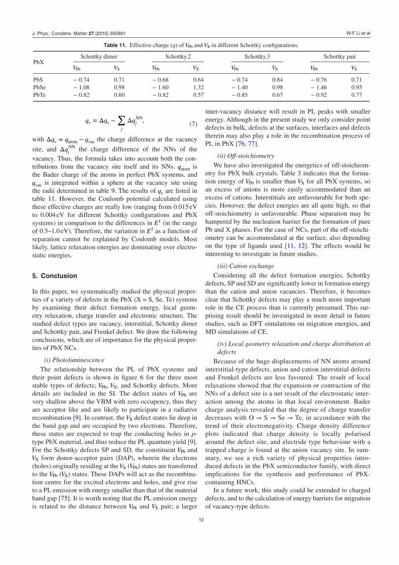
vacancy. Thus, the formula takes into account both the con-tributions from the vacancy site itself and its NNs. qatom is the Bader charge of the atoms in perfect PbX systems, and qvac is integrated within a sphere at the vacancy site using the radii determined in table 9. The results of qv are listed in table 11. However, the Coulomb potential calculated using these effective charges are really low (ranging from 0.015 eV to 0.004 eV for different Schottky configurations and PbX systems) in comparison to the differences in E f (in the range of 0.5–1.0 eV). Therefore, the variation in E f as a function of separation cannot be explained by Coulomb models. Most likely, lattice relaxation energies are dominating over electro-static energies.
5. Conclusion
In this paper, we systematically studied the physical proper-ties of a variety of defects in the PbX (X = S, Se, Te) systems by examining their defect formation energy, local geom-etry relaxation, charge transfer and electronic structure. The studied defect types are vacancy, interstitial, Schottky dimer and Schottky pair, and Frenkel defect. We draw the following conclusions, which are of importance for the physical proper-ties of PbX NCs.
(i) Photoluminescence
The relationship between the PL of PbX systems and their point defects is shown in figure 6 for the three most stable types of defects; VPb, VX, and Schottky defects. More details are included in the SI. The defect states of VPb are very shallow above the VBM with zero occupency, thus they are acceptor like and are likely to participate in a radiative recombination [9]. In contrast, the VX defect states lie deep in the band gap and are occupied by two electrons. Therefore, these states are expected to trap the conducting holes in p-type PbX material, and thus reduce the PL quantum yield [9]. For the Schottky defects SP and SD, the constituent VPb and VX form donor-acceptor pairs (DAP), wherein the electrons (holes) originally residing at the VX (VPb) states are transferred to the VPb (VX) states. These DAPs will act as the recombina-tion centre for the excited electrons and holes, and give rise to a PL emission with energy smaller than that of the material band gap [75]. It is worth noting that the PL emission energy is related to the distance between VPb and VX pair; a larger
inter-vacancy distance will result in PL peaks with smaller energy. Although in the present study we only consider point defects in bulk, defects at the surfaces, interfaces and defects therein may also play a role in the recombination process of PL in PbX [76, 77].
(ii) Off-stoichiometry
We have also investigated the energetics of off-stoichiom-etry for PbX bulk crystals. Table 3 indicates that the forma-tion energy of VPb is smaller than VX for all PbX systems, so an excess of anions is more easily accommodated than an excess of cations. Interstitials are unfavourable for both spe-cies. However, the defect energies are all quite high, so that off-stoichiometry is unfavourable. Phase separation may be hampered by the nucleation barrier for the formation of pure Pb and X phases. For the case of NCs, part of the off-stoichi-ometry can be accommodated at the surface, also depending on the type of ligands used [11, 12]. The effects would be interesting to investigate in future studies.
(iii) Cation exchange
Considering all the defect formation energies, Schottky defects, SP and SD are significantly lower in formation energy than the cation and anion vacancies. Therefore, it becomes clear that Schottky defects may play a much more important role in the CE process than is currently presumed. This sur-prising result should be investigated in more detail in future studies, such as DFT simulations on migration energies, and MD simulations of CE.
(iv) Local geometry relaxation and charge distribution at defects
Because of the huge displacements of NN atoms around interstitial-type defects, anion and cation interstitial defects and Frenkel defects are less favoured. The result of local relaxations showed that the expansion or contraction of the NNs of a defect site is a net result of the electrostatic inter-action among the atoms in that local environment. Bader charge analysis revealed that the degree of charge transfer decreases with O → S → Se → Te, in accordance with the trend of their electronegativity. Charge density difference plots indicated that charge density is locally polarised around the defect site, and electride type behaviour with a trapped charge is found at the anion vacancy site. In sum-mary, we see a rich variety of physical properties intro-duced defects in the PbX semiconductor family, with direct implications for the synthesis and performance of PbX-containing HNCs.
In a future work, this study could be extended to charged defects, and to the calculation of energy barriers for migration of vacancy-type defects.
Table 11. Effective charge (q) of VPb and VX in different Schottky configurations.
PbXSchottky dimer Schottky.2 Schottky.3 Schottky pair
VPb VX VPb VX VPb VX VPb VX
PbS − 0.74 0.71 − 0.68 0.64 − 0.74 0.84 − 0.76 0.71PbSe − 1.08 0.98 − 1.60 1.32 − 1.40 0.98 − 1.46 0.95PbTe − 0.82 0.60 − 0.82 0.57 − 0.85 0.67 − 0.92 0.77
J. Phys.: Condens. Matter 27 (2015) 355801

W-F Li et al
13
References
[1] Dalven R 1973 Solid State Physics vol 18 (New York: Academic)
[2] Dughaish Z H 2002 Lead telluride as a thermoelectric material for thermoelectric power generation Physica B 322 205
[3] Chaudhuri T K 1992 A solar thermophotovoltaic converter using PbS photovoltaic cells Int. J. Eng. Res. 16 481
[4] Preier H 1979 Recent advances in lead-chalcogenide diode lasers Appl. Phys. 20 189
[5] Chatterjee S and Pal U 1993 Low-cost solar selective absorbers from indian galena Opt. Eng. 32 2923
[6] Lee H et al 2009 PbS and CdS quantum dot-sensitized solid-state solar cells: old concepts, new results Adv. Funct. Mater. 19 2735
[7] Casavola M, van Huis M A, Bals S, Lambert K, Hens Z and Vanmaekelbergh D 2012 Anisotropic cation exchange in PbSe/CdSe core/shell nanocrystals of different geometry Chem. Mater. 24 294–302
[8] Groiss H et al 2007 Size control and midinfrared emission of epitaxial PbTe/CdTe quantum dot precipitates grown by molecular beam epitaxy Appl. Phys. Lett. 91 222106
[9] Gfroerer T H 2000 Photoluminescence in Analysis of Surfaces and Interfaces (Encyclopedia of Analytical Chemistry) (New York: Wiley)
[10] de Mello Donegá C 2011 Synthesis and properties of colloidal heteronanocrystals Chem. Soc. Rev. 40 1512
[11] Moreels I, Lambert K, De Muynck D, Vanhaecke F, Poelman D, Martins J C, Allan G and Hens Z 2007 Composition and size-dependent extinction coefficient of colloidal PbSe quantum dots Chem. Mater. 19 6101
[12] Moreels I, Martins B F J C and Hens Z 2008 Surface chemistry of colloidal PbSe nanocrystals J. Am. Chem. Soc. 130 15081
[13] Son D H, Hughes S M, Yin Y and Alivisatos A P 2004 Cation exchange reactions in ionic nanocrystals Science 306 1009
[14] Jain P K, Amirav L, Aloni S and Alivisatos A P 2010 Nanoheterostructure cation exchange: anionic framework conservation J. Am. Chem. Soc. 132 9997
[15] Li H, Zanella M, Genovese A, Povia M, Falqui A, Giannini C and Manna L 2011 Sequential cation exchange in nanocrystals: preservation of crystal phase and formation of metastable phases Nano Lett. 11 4964
[16] Miszta K, Dorfs D, Genovese A, Kim M R and Manna L 2011 Cation exchange reactions in colloidal branched nanocrystals ACS Nano 5 7176
[17] Bals S, Casavola M, van Huis M A, Van Aert S, Batenburg K J, Van Tendeloo G and Vanmaekelbergh D 2011 Three-dimensional atomic imaging of colloidal core-shell nanocrystals Nano Lett. 11 3420
[18] Groeneveld E, Witteman L, Lefferts M, Ke X, Bals S, Van Tendeloo G and de Mello Donega C 2013 Tailoring ZnSe–CdSe colloidal quantum dots via cation exchange: from core/shell to alloy nanocrystals ACS Nano 7 7913
[19] Sheng Y, Wei J, Liu B and Peng L 2014 A facile route to synthesize CdZnSe core-shell-like alloyed quantum dots via cation exchange reaction in aqueous system Mater. Res. Bull. 57 67
[20] Yalcin A O et al 2014 Atomic resolution monitoring of cation exchange in CdSe-PbSe heteronanocrystals during epitaxial solid–solid–vapor growth Nano Lett. 14 3661
[21] Ott F D, Spiegel L L, Norris D J and Erwin S C 2014 Microscopic theory of cation exchange in CdSe nanocrystals Phys. Rev. Lett. 113 156803
[22] Miller E, Komarek K and Cadoff I 1961 Interrelation of electronic properties and defect equilibria in PbTe J. Appl. Phys. 32 2457
[23] Polity A, Krause-Rehberg R, Zlomanov V, Stanov V and Chatchaturov A 1993 Study of vacancy defects in pbse and Pb1−xSnxSe by positron annihilation J. Cryst. Growth 131 271
[24] Khokhlov D 2002 Lead Chalcogenides: Physics and Applications (Boca Raton, FL: CRC Press)
[25] Yoneda S, Kato M and Ohsugi I J 2013 Anomaly in the specific heat of lead tellurides J. Theor. Appl. Phys. 7 11
[26] Zhang B, Cai C, Jin S, Ye Z, Wu H and Qi Z 2014 Resonant nature of intrinsic defect energy levels in PbTe revealed by infrared photoreflectance spectroscopy Appl. Phys. Lett. 105 022109
[27] Koumoulis D, Taylor R E, King D Jr and Bouchard L-S 2014 NMR study of native defects in PbSe Phys. Rev. B 90 125201
[28] Parada N J and Pratt G W Jr 1969 New model for vacancy states in PbTe Phys. Rev. Lett. 22 180
[29] Parada N J 1971 Localized defects in PbTe Phys. Rev. B 3 2042
[30] Lent C S, Bowen M A, Allgaier R S, Dow J D, Sankey O F and Ho E S 1987 Impurity levels in PbTe and Pb1−xSnxTe Solid State Commun. 61 83
[31] Ahmad S, Mahanti S D, Hoang K and Kanatzidis M G 2006 Ab initio studies of the electronic structure of defects in PbTe Phys. Rev. B 74 155205
[32] Ding Z-L, Xing H-Z, Xu S-L, Huang Y and Chen X-S 2007 First-principles study of electronic properties in PbS(1 0 0) with vacancy defect Chin. Phys. Lett. 24 3218
[33] Hoang K, Mahanti S D and Jena P 2007 Theoretical study of deep-defect states in bulk PbTe and in thin films Phys. Rev. B 76 115432
[34] Walsh A 2010 Defect processes in a PbS metal organic framework: a quantum-confined hybrid semiconductor J. Phys. Chem. Lett. 1 1284
[35] Peng H, Song J-H, Kanatzidis M G and Freeman A J 2011 Electronic structure and transport properties of doped PbSe Phys. Rev. B 84 125207
[36] Berashevich J, Semeniuk O, Rubel O, Rowlands J A and Reznik A 2013 Lead monoxide α-PbO: electronic properties and point defect formation J. Phys.: Condens. Matter 25 075803
[37] Wrasse E O, Bairerle R J, Fazzio A and Schmidt T M 2013 First-principles study of group iii impurity doped PbSe: bulk and nanowire Phys. Rev. B 87 085428
[38] Kim D, Kim D-H, Lee J-H and Grossman J C 2013 Impact of stoichiometry on the electronic structure of PbS quantum dots Phys. Rev. Lett. 110 196802
[39] Wei S-H and Zunger A 1997 Electronic and structural anomalies in lead chalcogenides Phys. Rev. B 55 13605
[40] Albanesi E A, Okoye C M I, Rodriguez C O and Peltzer E L 2000 Electronic structure, structural properties, and dielectric functions of IV–VI semiconductors: PbSe and PbTe Phys. Rev. B 61 16589
[41] Lach-hab M, Papaconstantopoulos D A and Mehl M J 2002 Electronic structure calculations of lead chalcogenides PbS, PbSe, PbTe J. Phys. Chem. Solids 63 833
[42] Hummer K, Grüneis A and Kresse G 2007 Structural and electronic properties of lead chalcogenides from first principles Phys. Rev. B 75 195211
[43] Zhang Y, Ke X, Chen C and Kent J P R C 2009 Thermodynamic properties of PbTe, PbSe, and PbS: first-principles study Phys. Rev. B 80 024304
[44] He J, Zhao L-D, Zheng J-C, Doak J W, Wu H, Wang H-Q, Lee Y, Wolverton C, Kanatzidis M G and Dravid V P 2013 Role of sodium doping in lead chalcogenide thermoelectrics J. Am. Chem. Soc. 135 4624
[45] Skelton J M, Parker S C, Togo A, Tanaka I and Walsh A 2014 Thermal physics of the lead chalcogenides PbS, PbSe, and PbTe from first principles Phys. Rev. B 89 205203
J. Phys.: Condens. Matter 27 (2015) 355801

W-F Li et al
14
[46] Walsh A and Watson G W 2005 Preparation of PbS-type PbO nanocrystals in a room-temperature ionic liquid J. Solid State Chem. 178 1422
[47] Kresse G and Hafner J 1994 Ab initio molecular-dynamics simulation of the liquid-metal-amorphous-semiconductor transition in germanium Phys. Rev. B 49 14251
[48] Kresse G and Furthmüller J 1996 Efficiency of ab initio total energy calculations for metals and semiconductors using a plane-wave basis set Comput. Mater. Sci. 6 15
[49] Kresse G and Furthmüller J 1996 Efficient iterative schemes for ab initio total-energy calculations using a plane-wave basis set Phys. Rev. B 54 11169
[50] Blochl P E 1994 Projector augmented-wave method Phys. Rev. B 50 17953
[51] Perdew J P, Burke K and Ernzerhof M 1996 Generalized gradient approximation made simple Phys. Rev. Lett. 77 3865
[52] Madelung O, Rössler U and Schulz M 2005 Semiconductors: Group IV Elements, IV–IV and III–IV Compounds (Landolt-Börnstein, New Series, Group III) vol 41 (Berlin: Springer)
[53] Perdew J P and Zunger A 1981 Self-interaction correction to density-functional approximations for many-electron systems Phys. Rev. B 23 5048
[54] Heyd J, Scuseria G E and Ernzerhof M 2003 Hybrid functionals based on a screened coulomb potential J. Chem. Phys 118 8207
[55] Constantin L A, Pitarke J M, Dobson J F, Garcia-Lekue A and Perdew J P 2008 High-level correlated approach to the jellium surface energy, without uniform-gas input Phys. Rev. Lett. 100 036401
[56] Svane A, Christensen N E, Cardona M, Chantis A N, van Schilfgaarde M and Kotani T 2010 Quasiparticle self-consistent GW calculations for PbS, PbSe, and PbTe: band structure and pressure coefficients Phys. Rev. B 81 245120
[57] Strehlow W H and Cook E L 1973 Compilation of energy band gaps in elemental and binary compound semiconductors and insulators J. Phys. Chem. Ref. Data 2 163
[58] Kullerrud G 1969 The lead–sulfur system Am. J. Sci. 267 233 [59] Lin J-C, Sharma R C and Chang Y A 1986 The Pb-S
(lead-sulfur) system Bull. Alloy Phase Diagr. 7 374 [60] Lin J-C, Sharma R C and Chang Y A 1996 The Pb-Se
(lead-selenium) system J. Phase Equilib. 17 253 [61] Lin J-C, Hsieh K-C, Sharma R C and Chang Y A 1989 The
Pb-Te (lead-tellurium) system Bull. Alloy Phase Diagr. 10 340
[62] Van de Walle C G and Neugebauer J 2004 First-principles calculations for defects and impurities: applications to III-nitrides J. Appl. Phys. 95 3581
[63] Oba F, Choi M, Togo A and Tanaka I 2011 Point defects in ZnO: an approach from first principles Sci. Technol. Adv. Mater. 12 034302
[64] Fang C M, van Huis M A, Jansen J and Zandbergen H W 2011 Role of carbon and nitrogen in Fe2C and Fe2N from first-principles calculations Phys. Rev. B 84 094102
[65] Fan Z, Yalcin A O, Tichelaar F D, Zandbergen H W, Talgorn E, Houtepen A J, Vlugt T J H and van Huis M A 2013 From sphere to multipod: thermally induced transitions of CdSe nanocrystals studied by molecular dynamics simulations J. Am. Chem. Soc. 135 5869
[66] Chai L et al 2013 Surfaces of colloidal PbSe nanocrystals probed by thin-film positron annihilation spectroscopy APL Mater. 11 02211
[67] Kutana A and Erwin S C 2011 PbSe nanocrystals remain intrinsic after surface adsorption of hydrazine Phys. Rev. B 83 235419
[68] Ullah N, Murtaza G, Khenata R, Hassan N, Naeem S, Khalid M N and Omran S B 2014 Structural and optoelectronic properties of PbSxSe1−x, PbSxTe1−x and PbSexTe1−x via first-principles calculations Comput. Mater. Sci. 83 496
[69] Shannon R D 1976 Revised effective ionic radii and systematic studies of interatomic distances in halides and chalcogenides Acta Cryst. A 32 751
[70] Li Z, Yang J, Hou J G and Zhu Q 2003 Inorganic electride: theoretical study on structural and electronic properties J. Am. Chem. Soc. 125 6050
[71] Dye J L 2003 Electrons as anions Science 301 607 [72] Kimoon L 2013 Dicalcium nitride as a two-dimensional
electride with an anionic electron layer Nature 494 336
[73] Dale S G, de-la Roza A O and Johnson E R 2014 Density-functional description of electrides Phys. Chem. Chem. Phys. 16 14584
[74] Smallenburg F, Filion L, Marechal M and Dijkstra M 2012 Vacancy-stabilized crystalline order in hard cubes Proc. Natl Acad. Sci. USA 109 17886
[75] Reshchikov M A and Morkoç H 2005 Luminescence properties of defects in gan J. Appl. Phys. 97 061301
[76] Krause M M, Mooney J and Kambhampati P 2013 Chemical and thermodynamic control of the surface of semiconductor nanocrystals for designer white light emitters ACS Nano 7 5922
[77] Voznyy O, Thon S M, Ip A H and Sargent E H 2013 Dynamic trap formation and elimination in colloidal quantum dots J. Phys. Chem. Lett. 4 987
J. Phys.: Condens. Matter 27 (2015) 355801