thermoelectric properties of highly-mismatched alloys · pdf file ·...
TRANSCRIPT
RSC Advances
PAPER
Thermoelectric p
aNew Technologies – Research Centre, Unive
14 Pilsen, Czech republic. E-mail: maalidphbCenter of Excellence Geopolymer and
Engineering, University Malaysia Perlis, 010
† Electronic supplementary informa10.1039/c6ra14685f
Cite this: RSC Adv., 2016, 6, 72286
Received 6th June 2016Accepted 22nd July 2016
DOI: 10.1039/c6ra14685f
www.rsc.org/advances
72286 | RSC Adv., 2016, 6, 72286–7229
roperties of highly-mismatchedalloys of GaNxAs1�x from first- to second-principlesmethods: energy conversion†
A. H. Reshak*ab
The transport properties of GaNxAs1�x (x ¼ 0.0, 0.25, 0.5, 0.75 and 1.0) alloys are investigated using the
semi-classical Boltzmann theory as implemented in the BoltzTraP code. The electronic structures are
calculated using the full potential linearized augmented plane wave method within the recently modified
Becke-Johnson potential to solve the exchange correlation potential. These alloys possess a direct band
gap varying between 0.5 and 3.2 eV. The ‘special quasi-random structures’ approach of Zunger was used
to reproduce the randomness of the GaNxAs1�x alloys for the first few shells around a given site. The
carrier concentration (n), electrical conductivity (s/s), Seebeck coefficient (S), electronic thermal
conductivity (ke/s) and the electronic power factor (S2s/s), as a function of temperature were obtained
for GaNxAs1�x alloys. In addition, the transport properties as a function of chemical potential at three
constant temperatures were investigated. It has been found that GaNxAs1�x alloys show good transport
properties, therefore, we expect that these alloys could be possible potential candidates for clean energy
applications.
1. Introduction
Thermoelectric power generators can convert heat into elec-tricity, which is a good alternative solution for energy andenvironment problems.1 Ever since this discovery, extensivestudies were done on several materials to enhance their ther-moelectric properties for technological applications.2–11 Thedevelopment of novel thermoelectric materials has attracteda great deal of interest due to their signicant potential appli-cations ranging from clean energy to photon sensing devices.The efficient thermoelectric materials can be classied intothree types: complex crystals, alloys and nano-crystals.12 Theycan provide a signicant contribution to solve global sustain-able energy problems. Thermoelectric materials play animportant role in global sustainable energy solutions. Thesematerials are not only used in generating electricity from wasteheat but also used as solid-state Peltier coolers.12 In the complexcrystals category there are ternary alloys such as GaNxAs1�x.These can be considered to be possible potential candidates forapplications in optoelectronic, semiconductor lasers, andoptical detectors.13–19 It was found that the electronic structureand optical properties of GaAs are modied signicantly when
rsity of West Bohemia, Univerzitni 8, 306
@yahoo.co.uk; Tel: +420 777 729 583
Green Technology, School of Material
07 Kangar, Perlis, Malaysia
tion (ESI) available. See DOI:
4
a small concentration of N doped into GaAs. There is a signi-cant increase in the band gap when As is replaced by N.20 It wasreported that nitrogen in GaNAs perturbs the conduction bandsand reduces electron mobility21–23 because nitrogen is highlyelectronegative (3.04) in addition to its small size, and it isattractive to electrons, in comparison to the size and the elec-tronegativity of As (2.18).
Several workers have reported the inuence of vary thecontent of N on the electronic properties of the doped alloys.Since the energy gap is in the range 0.5–1.5 eV, these alloyscould have a potential application in thermoelectric devices. Asa natural extension to our previous work on the electronicstructure24 and the nonlinear optical properties of GaNxAs1�x
alloys,25 we thought it would be interesting to study the trans-port properties of GaNxAs1�x alloys.
2. Computational method
The all electron full potential linearized augmented plan waveplus local orbital (FP � L(APW + lo)) method26 within densityfunctional theory (DFT) and the semi-classical Boltzmanntheory as implemented in the BoltzTraP code27 were used tocalculate the transport properties of GaNxAs1�x alloys with x ¼0.0, 0.25, 0.5, 0.75 and 1.0. The recently modied Becke-Johnson potential (mBJ)28 was used to solve the exchangecorrelation functional. In calculating the self-consistent bandstructure within DFT, both local-density approximation (LDA)29
and the generalized-gradient (GGA)30 usually underestimate theenergy gap.31 This is mainly due to the fact that they have simple
This journal is © The Royal Society of Chemistry 2016

Paper RSC Advances
forms that are not sufficiently exible to accurately reproduceboth the exchange-correlation energy and its charge derivative.To overcome this drawback we proposed mBJ. The mBJ,a modied Becke-Johnson potential, allows the calculation ofband gaps with accuracy similar to the very expensive GWcalculations.28 It is a local approximation to an atomic “exact-exchange” potential and a screening term.
The number of basis functions were used up to RMTKmax ¼7.0 (where RMT is the minimum radius of the muffin-tin spheresand Kmax gives the magnitude of the largest k vector in the planewave expansion). The values of the sphere radii and Kmax arekept constant over all the range of lattice spacing. The Fourierexpanded charge density was truncated at Gmax ¼ 14 (Ryd)1/2. Inorder to reproduce the randomness of the alloys for the rst fewshells around a given site, the ‘special quasi-random structures’(SQS) approach of Zunger et al.32 was used. We would like tomention here for the composition x ¼ 0.25 and 0.75 thesimplest structure is an eight-atom simple cubic lattice(luzonite): the cations with the lower concentration forma regular simple cubic lattice (see Fig. 1(b) and (d)). For x ¼ 0.5composition, the smallest ordered structure is (001) super-cell(see Fig. 1(c)). The muffin-tin radii for the composition x ¼0.25 and 0.75 are 1.95, 1.9 and 1.6 atomic units (a.u.) for Ga, Asand N respectively. For x ¼ 0.5 the muffin-tin radii was set to be2.14 a.u. for Ga, N and As. A mesh of 35 special k-points wasused for ternary alloys except for the case of x ¼ 0.5, where weused a mesh of 64 special k-points in the irreducible Brillouinzone (IBZ). For calculating the transport properties of GaNx-As1�x alloys a denser meshes of 50 000 k-points in IBZ for theternary alloys were used. The self-consistent calculations are
Fig. 1 The structure of the unit cell of GaNxAs1�x (x ¼ 0.0, 0.25, 0.5, 0.75cubic lattice (luzonite): the cations with the lower concentration form aordered structure is (001) super-cell.
This journal is © The Royal Society of Chemistry 2016
converged since the total energy of the system is stable within10�5 Ry.
We have used the semi-classical Boltzmann theory asincorporated in BoltzTraP code27 to calculate the thermoelectricproperties. The transport coefficients that based on rigid bandapproach to conductivity is given by;
sabð3Þ ¼ 1
N
Xi;k
sabði; kÞ dð3� 3i;kÞd3
(1)
sab(i,~k) ¼ e2si,~kwa(i,~k)wb(i,~k) (2)
sabð3Þ ¼ e2
N
Xi;k
si;~k wa
�i; ~k
�wb
�i; ~k
�dð3� 3i;kÞ (3)
where e represent charge of electron, s is the relaxation time,a and b are the tensor indices, N is the number of k-points,wa(i,~k) and wb(i,~k) are the group velocities. It is important tomention that in BoltzTraP code the relaxation time s taken asa constant.27 The transport coefficients can be written asa function of temperature and chemical potential27,33 as follow;
sabðT ;mÞ ¼ 1
U
ðsabð3Þ
�� vf0ðT ; 3;mÞ
v3
�d3 (4)
SabðT ;mÞ ¼ 1
eTUsabðT ;mÞðsabð3Þð3� mÞ �
�� vf0ðT ; 3;mÞ
v3
�d3
(5)
k0abðT ;mÞ ¼ 1
e2TU
ðsabð3Þð3� mÞ2
�� vf0ðT ; 3;mÞ
v3
�d3 (6)
and 1.0) alloys; (b and d) the simplest structure is an eight-atom simpleregular simple cubic lattice; (c) for x ¼ 0.5 composition, the smallest
RSC Adv., 2016, 6, 72286–72294 | 72287
RSC Advances Paper
whereU stands for volume of the unit cell, and f0 is Fermi–Diracdistribution function. To gain high thermoelectric efficiency, itis important that the material possess high electrical conduc-tivity, large Seebeck coefficient and low thermal conductivity.34
Simulations of the transport properties is transition fromrst- to second-principles methods. The rst-principles methodused here is all-electron full potential linear augmented planewave method whereas the second-principles is BoltzTraP code,27
which solves the semi-classical Bloch–Boltzmann transportequations.27 Transport properties were obtained from theground state within the limits of Boltzmann theory35–37 and theconstant relaxation time approximation as implemented in theBoltzTraP code.27 In short, BoltzTraP performs a Fourierexpansion of the quantum chemical band energies. This allowsto obtain the electronic group velocity and inverse mass tensor,
Fig. 2 The calculated electronic band stature of GaNxAs1�x (x ¼ 0.0, 0.2
72288 | RSC Adv., 2016, 6, 72286–72294
as the rst and second derivatives of the bands with respect to k.Applying the electronic group velocity and inverse mass tensorto the semiclassical Boltzmann equations, the transport tensorscan be evaluated.
3. Results and discussion3.1. Salient features of the electronic band structures
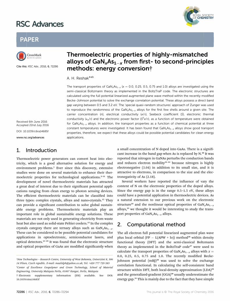
Since the electronic band structures are very important forcalculating the effective mass and the transport properties,therefore we will recall the main features of the electronic bandstructure of GaNxAs1�x (x¼ 0.0, 0.25, 0.50, 0.75 and 1.0) alloys.24
Fig. 2(a–e) shows the electronic band structure along the highsymmetry points of the rst Brillouin zone. We set the zero-point of energy (Fermi level) at the valence band maximum
5, 0.5, 0.75 and 1.0) alloys, using mBJ.
This journal is © The Royal Society of Chemistry 2016
Paper RSC Advances
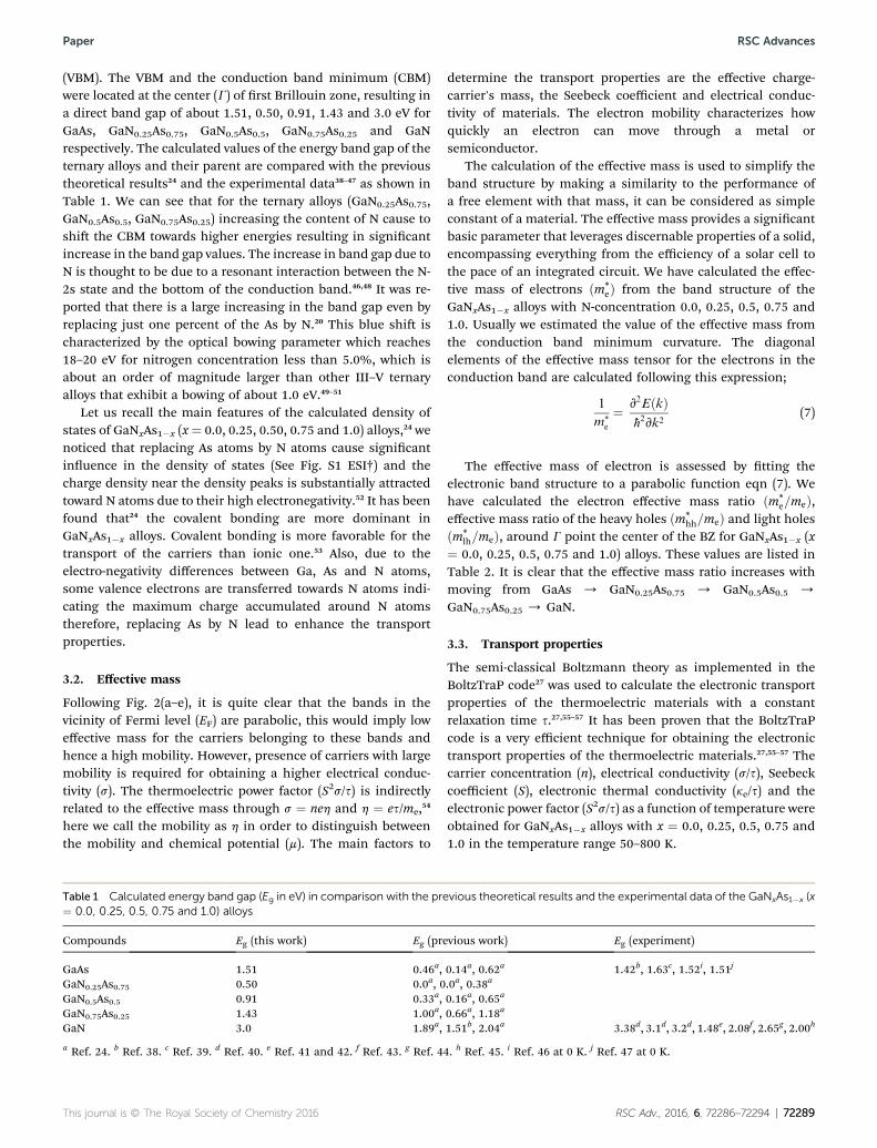
(VBM). The VBM and the conduction band minimum (CBM)were located at the center (G) of rst Brillouin zone, resulting ina direct band gap of about 1.51, 0.50, 0.91, 1.43 and 3.0 eV forGaAs, GaN0.25As0.75, GaN0.5As0.5, GaN0.75As0.25 and GaNrespectively. The calculated values of the energy band gap of theternary alloys and their parent are compared with the previoustheoretical results24 and the experimental data38–47 as shown inTable 1. We can see that for the ternary alloys (GaN0.25As0.75,GaN0.5As0.5, GaN0.75As0.25) increasing the content of N cause toshi the CBM towards higher energies resulting in signicantincrease in the band gap values. The increase in band gap due toN is thought to be due to a resonant interaction between the N-2s state and the bottom of the conduction band.46,48 It was re-ported that there is a large increasing in the band gap even byreplacing just one percent of the As by N.20 This blue shi ischaracterized by the optical bowing parameter which reaches18–20 eV for nitrogen concentration less than 5.0%, which isabout an order of magnitude larger than other III–V ternaryalloys that exhibit a bowing of about 1.0 eV.49–51
Let us recall the main features of the calculated density ofstates of GaNxAs1�x (x¼ 0.0, 0.25, 0.50, 0.75 and 1.0) alloys,24 wenoticed that replacing As atoms by N atoms cause signicantinuence in the density of states (See Fig. S1 ESI†) and thecharge density near the density peaks is substantially attractedtoward N atoms due to their high electronegativity.52 It has beenfound that24 the covalent bonding are more dominant inGaNxAs1�x alloys. Covalent bonding is more favorable for thetransport of the carriers than ionic one.53 Also, due to theelectro-negativity differences between Ga, As and N atoms,some valence electrons are transferred towards N atoms indi-cating the maximum charge accumulated around N atomstherefore, replacing As by N lead to enhance the transportproperties.
3.2. Effective mass
Following Fig. 2(a–e), it is quite clear that the bands in thevicinity of Fermi level (EF) are parabolic, this would imply loweffective mass for the carriers belonging to these bands andhence a high mobility. However, presence of carriers with largemobility is required for obtaining a higher electrical conduc-tivity (s). The thermoelectric power factor (S2s/s) is indirectlyrelated to the effective mass through s ¼ neh and h ¼ es/me,54
here we call the mobility as h in order to distinguish betweenthe mobility and chemical potential (m). The main factors to
Table 1 Calculated energy band gap (Eg in eV) in comparison with the pr¼ 0.0, 0.25, 0.5, 0.75 and 1.0) alloys
Compounds Eg (this work) Eg (pr
GaAs 1.51 0.46a,GaN0.25As0.75 0.50 0.0a, 0GaN0.5As0.5 0.91 0.33a,GaN0.75As0.25 1.43 1.00a,GaN 3.0 1.89a,
a Ref. 24. b Ref. 38. c Ref. 39. d Ref. 40. e Ref. 41 and 42. f Ref. 43. g Ref. 4
This journal is © The Royal Society of Chemistry 2016
determine the transport properties are the effective charge-carrier's mass, the Seebeck coefficient and electrical conduc-tivity of materials. The electron mobility characterizes howquickly an electron can move through a metal orsemiconductor.
The calculation of the effective mass is used to simplify theband structure by making a similarity to the performance ofa free element with that mass, it can be considered as simpleconstant of a material. The effective mass provides a signicantbasic parameter that leverages discernable properties of a solid,encompassing everything from the efficiency of a solar cell tothe pace of an integrated circuit. We have calculated the effec-tive mass of electrons ðm*
eÞ from the band structure of theGaNxAs1�x alloys with N-concentration 0.0, 0.25, 0.5, 0.75 and1.0. Usually we estimated the value of the effective mass fromthe conduction band minimum curvature. The diagonalelements of the effective mass tensor for the electrons in theconduction band are calculated following this expression;
1
m*e
¼ v2EðkÞħ2vk2
(7)
The effective mass of electron is assessed by tting theelectronic band structure to a parabolic function eqn (7). Wehave calculated the electron effective mass ratio ðm*
e=meÞ,effective mass ratio of the heavy holes ðm*
hh=meÞ and light holesðm*
lh=meÞ, around G point the center of the BZ for GaNxAs1�x (x¼ 0.0, 0.25, 0.5, 0.75 and 1.0) alloys. These values are listed inTable 2. It is clear that the effective mass ratio increases withmoving from GaAs / GaN0.25As0.75 / GaN0.5As0.5 /
GaN0.75As0.25 / GaN.
3.3. Transport properties
The semi-classical Boltzmann theory as implemented in theBoltzTraP code27 was used to calculate the electronic transportproperties of the thermoelectric materials with a constantrelaxation time s.27,55–57 It has been proven that the BoltzTraPcode is a very efficient technique for obtaining the electronictransport properties of the thermoelectric materials.27,55–57 Thecarrier concentration (n), electrical conductivity (s/s), Seebeckcoefficient (S), electronic thermal conductivity (ke/s) and theelectronic power factor (S2s/s) as a function of temperature wereobtained for GaNxAs1�x alloys with x ¼ 0.0, 0.25, 0.5, 0.75 and1.0 in the temperature range 50–800 K.
evious theoretical results and the experimental data of the GaNxAs1�x (x
evious work) Eg (experiment)
0.14a, 0.62a 1.42b, 1.63c, 1.52i, 1.51j
.0a, 0.38a
0.16a, 0.65a
0.66a, 1.18a
1.51b, 2.04a 3.38d, 3.1d, 3.2d, 1.48e, 2.08f, 2.65g, 2.00h
4. h Ref. 45. i Ref. 46 at 0 K. j Ref. 47 at 0 K.
RSC Adv., 2016, 6, 72286–72294 | 72289
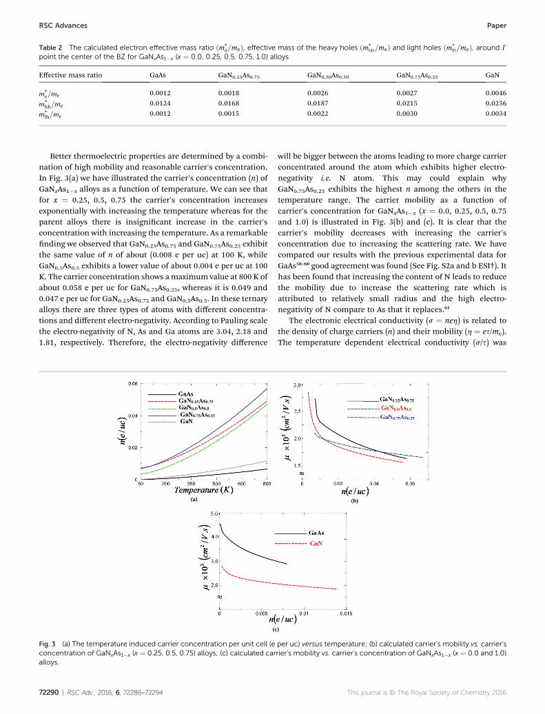
Table 2 The calculated electron effective mass ratio ðm*e=meÞ, effective mass of the heavy holes ðm*
hh=meÞ and light holes ðm*lh=meÞ, around G
point the center of the BZ for GaNxAs1�x (x ¼ 0.0, 0.25, 0.5, 0.75, 1.0) alloys
Effective mass ratio GaAs GaN0.25As0.75 GaN0.50As0.50 GaN0.75As0.25 GaN
m*e=me 0.0012 0.0018 0.0026 0.0027 0.0046
m*hh=me 0.0124 0.0168 0.0187 0.0215 0.0256
m*lh=me 0.0012 0.0015 0.0022 0.0030 0.0034
RSC Advances Paper
Better thermoelectric properties are determined by a combi-nation of high mobility and reasonable carrier's concentration.In Fig. 3(a) we have illustrated the carrier's concentration (n) ofGaNxAs1�x alloys as a function of temperature. We can see thatfor x ¼ 0.25, 0.5, 0.75 the carrier's concentration increasesexponentially with increasing the temperature whereas for theparent alloys there is insignicant increase in the carrier'sconcentration with increasing the temperature. As a remarkablending we observed that GaN0.25As0.75 and GaN0.75As0.25 exhibitthe same value of n of about (0.008 e per uc) at 100 K, whileGaN0.5As0.5 exhibits a lower value of about 0.004 e per uc at 100K. The carrier concentration shows amaximum value at 800 K ofabout 0.058 e per uc for GaN0.75As0.25, whereas it is 0.049 and0.047 e per uc for GaN0.25As0.75 and GaN0.5As0.5. In these ternaryalloys there are three types of atoms with different concentra-tions and different electro-negativity. According to Pauling scalethe electro-negativity of N, As and Ga atoms are 3.04, 2.18 and1.81, respectively. Therefore, the electro-negativity difference
Fig. 3 (a) The temperature induced carrier concentration per unit cell (econcentration of GaNxAs1�x (x ¼ 0.25, 0.5, 0.75) alloys; (c) calculated caralloys.
72290 | RSC Adv., 2016, 6, 72286–72294
will be bigger between the atoms leading to more charge carrierconcentrated around the atom which exhibits higher electro-negativity i.e. N atom. This may could explain whyGaN0.75As0.25 exhibits the highest n among the others in thetemperature range. The carrier mobility as a function ofcarrier's concentration for GaNxAs1�x (x ¼ 0.0, 0.25, 0.5, 0.75and 1.0) is illustrated in Fig. 3(b) and (c). It is clear that thecarrier's mobility decreases with increasing the carrier'sconcentration due to increasing the scattering rate. We havecompared our results with the previous experimental data forGaAs58–60 good agreement was found (See Fig. S2a and b ESI†). Ithas been found that increasing the content of N leads to reducethe mobility due to increase the scattering rate which isattributed to relatively small radius and the high electro-negativity of N compare to As that it replaces.61
The electronic electrical conductivity (s ¼ neh) is related tothe density of charge carriers (n) and their mobility (h ¼ es/me).The temperature dependent electrical conductivity (s/s) was
per uc) versus temperature; (b) calculated carrier's mobility vs. carrier'srier's mobility vs. carrier's concentration of GaNxAs1�x (x ¼ 0.0 and 1.0)
This journal is © The Royal Society of Chemistry 2016
Paper RSC Advances
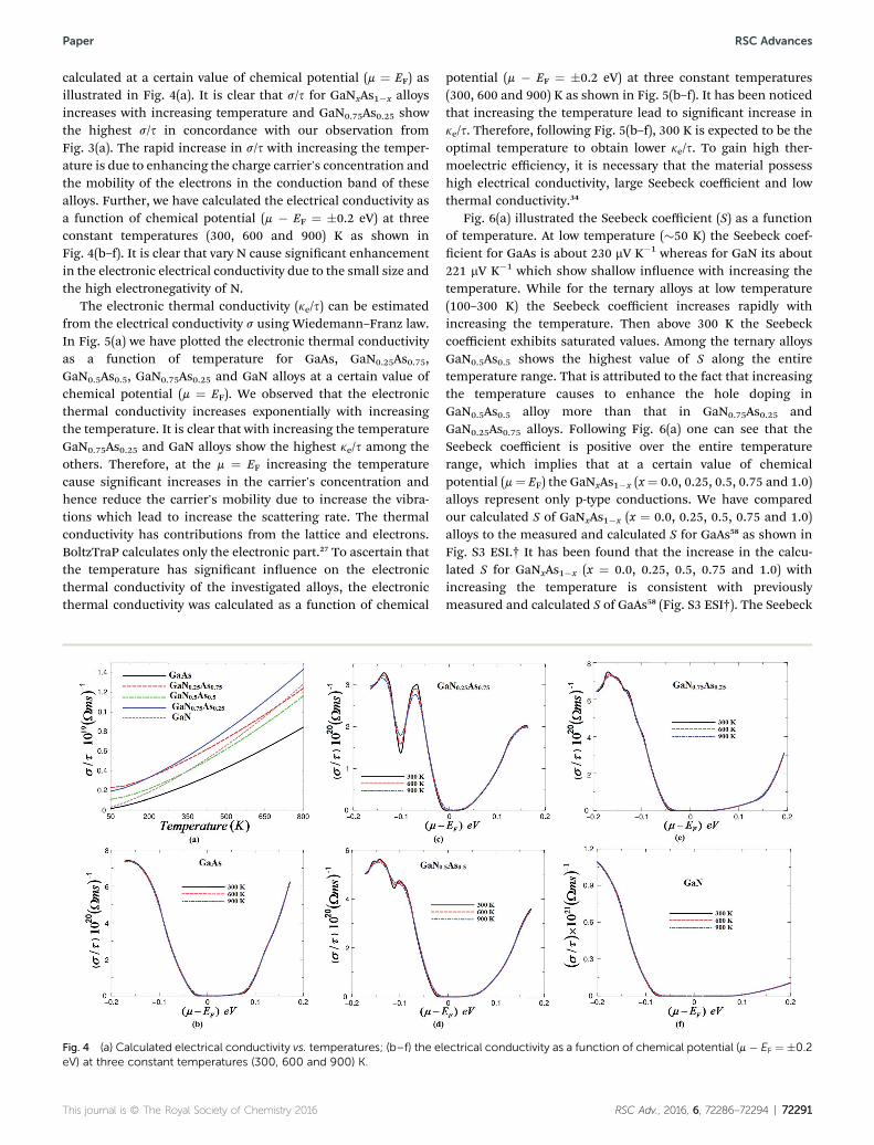
calculated at a certain value of chemical potential (m ¼ EF) asillustrated in Fig. 4(a). It is clear that s/s for GaNxAs1�x alloysincreases with increasing temperature and GaN0.75As0.25 showthe highest s/s in concordance with our observation fromFig. 3(a). The rapid increase in s/s with increasing the temper-ature is due to enhancing the charge carrier's concentration andthe mobility of the electrons in the conduction band of thesealloys. Further, we have calculated the electrical conductivity asa function of chemical potential (m � EF ¼ �0.2 eV) at threeconstant temperatures (300, 600 and 900) K as shown inFig. 4(b–f). It is clear that vary N cause signicant enhancementin the electronic electrical conductivity due to the small size andthe high electronegativity of N.
The electronic thermal conductivity (ke/s) can be estimatedfrom the electrical conductivity s using Wiedemann–Franz law.In Fig. 5(a) we have plotted the electronic thermal conductivityas a function of temperature for GaAs, GaN0.25As0.75,GaN0.5As0.5, GaN0.75As0.25 and GaN alloys at a certain value ofchemical potential (m ¼ EF). We observed that the electronicthermal conductivity increases exponentially with increasingthe temperature. It is clear that with increasing the temperatureGaN0.75As0.25 and GaN alloys show the highest ke/s among theothers. Therefore, at the m ¼ EF increasing the temperaturecause signicant increases in the carrier's concentration andhence reduce the carrier's mobility due to increase the vibra-tions which lead to increase the scattering rate. The thermalconductivity has contributions from the lattice and electrons.BoltzTraP calculates only the electronic part.27 To ascertain thatthe temperature has signicant inuence on the electronicthermal conductivity of the investigated alloys, the electronicthermal conductivity was calculated as a function of chemical
Fig. 4 (a) Calculated electrical conductivity vs. temperatures; (b–f) the eleV) at three constant temperatures (300, 600 and 900) K.
This journal is © The Royal Society of Chemistry 2016
potential (m � EF ¼ �0.2 eV) at three constant temperatures(300, 600 and 900) K as shown in Fig. 5(b–f). It has been noticedthat increasing the temperature lead to signicant increase inke/s. Therefore, following Fig. 5(b–f), 300 K is expected to be theoptimal temperature to obtain lower ke/s. To gain high ther-moelectric efficiency, it is necessary that the material possesshigh electrical conductivity, large Seebeck coefficient and lowthermal conductivity.34
Fig. 6(a) illustrated the Seebeck coefficient (S) as a functionof temperature. At low temperature (�50 K) the Seebeck coef-cient for GaAs is about 230 mV K�1 whereas for GaN its about221 mV K�1 which show shallow inuence with increasing thetemperature. While for the ternary alloys at low temperature(100–300 K) the Seebeck coefficient increases rapidly withincreasing the temperature. Then above 300 K the Seebeckcoefficient exhibits saturated values. Among the ternary alloysGaN0.5As0.5 shows the highest value of S along the entiretemperature range. That is attributed to the fact that increasingthe temperature causes to enhance the hole doping inGaN0.5As0.5 alloy more than that in GaN0.75As0.25 andGaN0.25As0.75 alloys. Following Fig. 6(a) one can see that theSeebeck coefficient is positive over the entire temperaturerange, which implies that at a certain value of chemicalpotential (m¼ EF) the GaNxAs1�x (x¼ 0.0, 0.25, 0.5, 0.75 and 1.0)alloys represent only p-type conductions. We have comparedour calculated S of GaNxAs1�x (x ¼ 0.0, 0.25, 0.5, 0.75 and 1.0)alloys to the measured and calculated S for GaAs58 as shown inFig. S3 ESI.† It has been found that the increase in the calcu-lated S for GaNxAs1�x (x ¼ 0.0, 0.25, 0.5, 0.75 and 1.0) withincreasing the temperature is consistent with previouslymeasured and calculated S of GaAs58 (Fig. S3 ESI†). The Seebeck
ectrical conductivity as a function of chemical potential (m � EF ¼ �0.2
RSC Adv., 2016, 6, 72286–72294 | 72291
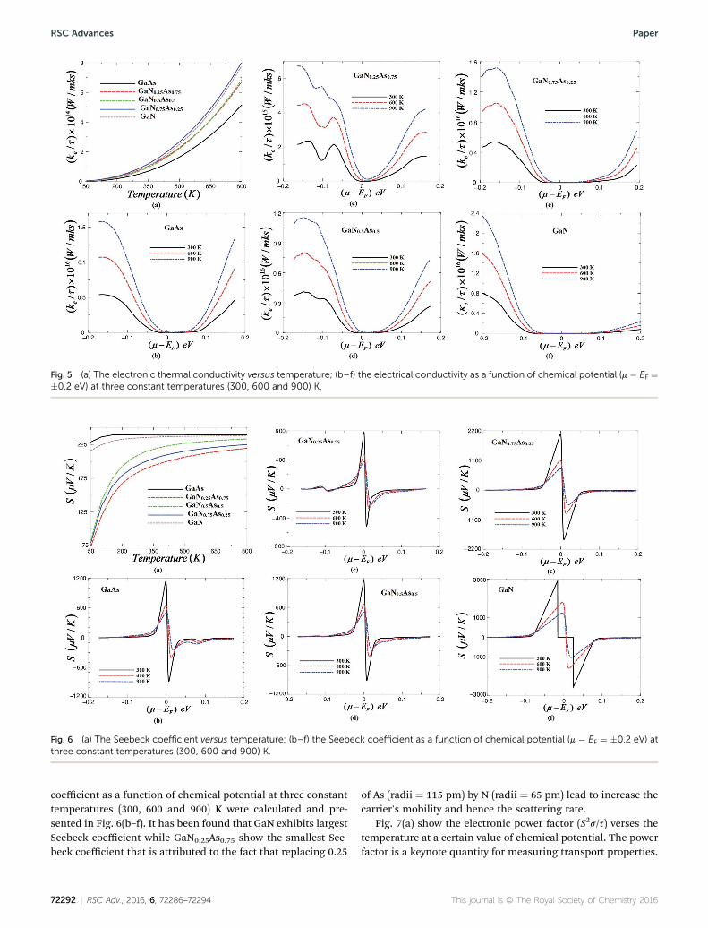
Fig. 5 (a) The electronic thermal conductivity versus temperature; (b–f) the electrical conductivity as a function of chemical potential (m � EF ¼�0.2 eV) at three constant temperatures (300, 600 and 900) K.
Fig. 6 (a) The Seebeck coefficient versus temperature; (b–f) the Seebeck coefficient as a function of chemical potential (m � EF ¼ �0.2 eV) atthree constant temperatures (300, 600 and 900) K.
RSC Advances Paper
coefficient as a function of chemical potential at three constanttemperatures (300, 600 and 900) K were calculated and pre-sented in Fig. 6(b–f). It has been found that GaN exhibits largestSeebeck coefficient while GaN0.25As0.75 show the smallest See-beck coefficient that is attributed to the fact that replacing 0.25
72292 | RSC Adv., 2016, 6, 72286–72294
of As (radii ¼ 115 pm) by N (radii ¼ 65 pm) lead to increase thecarrier's mobility and hence the scattering rate.
Fig. 7(a) show the electronic power factor (S2s/s) verses thetemperature at a certain value of chemical potential. The powerfactor is a keynote quantity for measuring transport properties.
This journal is © The Royal Society of Chemistry 2016
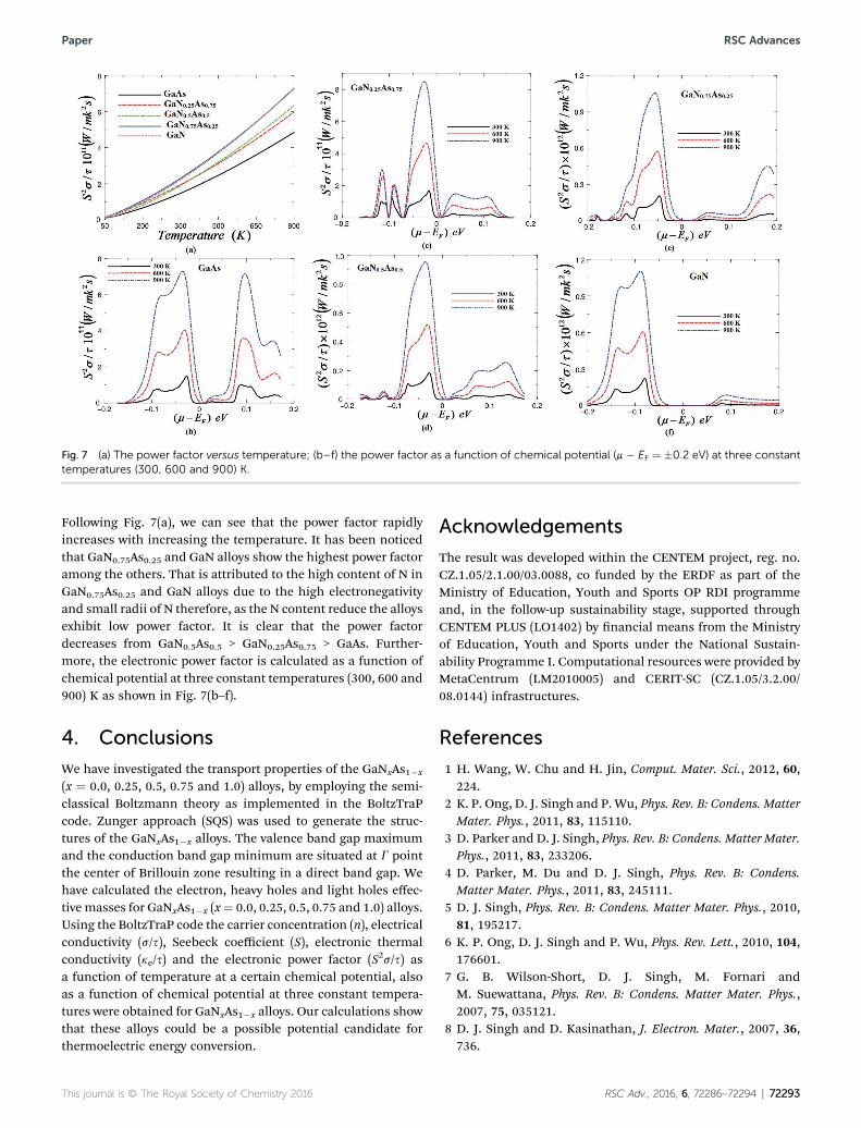
Fig. 7 (a) The power factor versus temperature; (b–f) the power factor as a function of chemical potential (m � EF ¼ �0.2 eV) at three constanttemperatures (300, 600 and 900) K.
Paper RSC Advances
Following Fig. 7(a), we can see that the power factor rapidlyincreases with increasing the temperature. It has been noticedthat GaN0.75As0.25 and GaN alloys show the highest power factoramong the others. That is attributed to the high content of N inGaN0.75As0.25 and GaN alloys due to the high electronegativityand small radii of N therefore, as the N content reduce the alloysexhibit low power factor. It is clear that the power factordecreases from GaN0.5As0.5 > GaN0.25As0.75 > GaAs. Further-more, the electronic power factor is calculated as a function ofchemical potential at three constant temperatures (300, 600 and900) K as shown in Fig. 7(b–f).
4. Conclusions
We have investigated the transport properties of the GaNxAs1�x
(x ¼ 0.0, 0.25, 0.5, 0.75 and 1.0) alloys, by employing the semi-classical Boltzmann theory as implemented in the BoltzTraPcode. Zunger approach (SQS) was used to generate the struc-tures of the GaNxAs1�x alloys. The valence band gap maximumand the conduction band gap minimum are situated at G pointthe center of Brillouin zone resulting in a direct band gap. Wehave calculated the electron, heavy holes and light holes effec-tive masses for GaNxAs1�x (x¼ 0.0, 0.25, 0.5, 0.75 and 1.0) alloys.Using the BoltzTraP code the carrier concentration (n), electricalconductivity (s/s), Seebeck coefficient (S), electronic thermalconductivity (ke/s) and the electronic power factor (S2s/s) asa function of temperature at a certain chemical potential, alsoas a function of chemical potential at three constant tempera-tures were obtained for GaNxAs1�x alloys. Our calculations showthat these alloys could be a possible potential candidate forthermoelectric energy conversion.
This journal is © The Royal Society of Chemistry 2016
Acknowledgements
The result was developed within the CENTEM project, reg. no.CZ.1.05/2.1.00/03.0088, co funded by the ERDF as part of theMinistry of Education, Youth and Sports OP RDI programmeand, in the follow-up sustainability stage, supported throughCENTEM PLUS (LO1402) by nancial means from the Ministryof Education, Youth and Sports under the National Sustain-ability Programme I. Computational resources were provided byMetaCentrum (LM2010005) and CERIT-SC (CZ.1.05/3.2.00/08.0144) infrastructures.
References
1 H. Wang, W. Chu and H. Jin, Comput. Mater. Sci., 2012, 60,224.
2 K. P. Ong, D. J. Singh and P. Wu, Phys. Rev. B: Condens. MatterMater. Phys., 2011, 83, 115110.
3 D. Parker and D. J. Singh, Phys. Rev. B: Condens. Matter Mater.Phys., 2011, 83, 233206.
4 D. Parker, M. Du and D. J. Singh, Phys. Rev. B: Condens.Matter Mater. Phys., 2011, 83, 245111.
5 D. J. Singh, Phys. Rev. B: Condens. Matter Mater. Phys., 2010,81, 195217.
6 K. P. Ong, D. J. Singh and P. Wu, Phys. Rev. Lett., 2010, 104,176601.
7 G. B. Wilson-Short, D. J. Singh, M. Fornari andM. Suewattana, Phys. Rev. B: Condens. Matter Mater. Phys.,2007, 75, 035121.
8 D. J. Singh and D. Kasinathan, J. Electron. Mater., 2007, 36,736.
RSC Adv., 2016, 6, 72286–72294 | 72293

RSC Advances Paper
9 D. J. Singh, Phys. Rev. B: Condens. Matter Mater. Phys., 2007,76, 085110.
10 D. J. Singh, Oxide Thermoelectrics, MRS Symp. Proc, 2008,vol. 1044, pp. U02–U05.
11 D. J. Singh, Alkaline earth lled nickel skutteruditeantimonide thermoelectrics, US Pat., 8,487,178, 2013.
12 H. A. R. Aliabad, M. Ghazanfari, I. Ahmad and M. A. Saeed,Comput. Mater. Sci., 2012, 65, 509.
13 J. W. Orton and C. T. Foxon, Rep. Prog. Phys., 1998, 61, 1.14 S. C. Jain, M. Willander, J. Narayan and R. V. Overstraeten, J.
Appl. Phys., 2000, 87, 965.15 I. Vurgaman and J. R. Meyer, J. Appl. Phys., 2003, 94, 3675.16 H. P. Xin and C. W. Tu, Appl. Phys. Lett., 1998, 72, 2442.17 W. Shan, W. Walukiewicz, J. W. Ager III, E. E. Haller,
J. F. Geisz, D. J. Friedman, J. M. Olson and S. R. Kurtz,Phys. Rev. Lett., 1999, 82, 1221.
18 M. Kondow, K. Uomi, A. Niwa, T. Kitatani, S. Watahiki andY. Yazawa, Jpn. J. Appl. Phys., 1996, 35, 1273.
19 M. Bissiri, V. Gaspari, A. Polimeni, G. B. H. von Hogersthal,M. Capizzi and A. Frova, Appl. Phys. Lett., 2001, 79, 2585.
20 M. Weyers, M. Sato and H. Ando, Jpn. J. Appl. Phys., 1992, 31,L853.
21 W. Shan, W. Walukiwiecz, J. W. Ager, E. E. Haller, J. F. Geisz,D. J. Fiedman, J. M. Olson and S. R. Kurtz, Phys. Rev. Lett.,1999, 82, 1221.
22 S. Fahy and E. P. O'Reilly, Appl. Phys. Lett., 2003, 83, 3731.23 A. Lindsay, E. P. O'Reilly, A. D. Andreev and T. Ashley, Phys.
Rev. B: Condens. Matter Mater. Phys., 2008, 77, 165205.24 H. Baaziz, Z. Chari, A. H. Reshak, B. Hamad and Y. Al-
Douri, Appl. Phys. A: Mater. Sci. Process., 2012, 106, 687.25 A. H. Reshak, J. Alloys Compd., 2014, 589, 213.26 P. Blaha, K. Schwarz, G. K. H. Madsen, D. Kvasnicka and
J. Luitz, Wien2k, An Augmented Plane Wave Plus LocalOrbitals Program for Crystal Properties, Vienna University ofTechnology, Vienna, Austria, 2001.
27 G. K. H. Madsen and D. J. Singh, Comput. Phys. Commun.,2006, 175, 67.
28 F. Tran and P. Blaha, Phys. Rev. Lett., 2009, 102, 226401.29 W. Kohn and L. J. Sham, Phys. Rev. A, 1965, 140, 1133.30 J. P. Perdew, S. Burke and M. Ernzerhof, Phys. Rev. Lett.,
1996, 77, 3865.31 P. Dufek, P. Blaha and K. Schwarz, Phys. Rev. B: Condens.
Matter Mater. Phys., 1994, 50, 7279.32 A. Zunger, S.-H. Wei, L. G. Feireira and J. E. Bernard, Phys.
Rev. Lett., 1990, 65, 353.33 T. J. Scheidemantel, C. Ambrosch-Draxl, T. Thonhauser,
J. V. Badding and J. O. Sofo, Phys. Rev. B: Condens. MatterMater. Phys., 2003, 68, 125210.
34 G. J. Snyder and E. S. Toberer, Nat. Mater., 2008, 7, 105–114.35 P. B. Allen, in Quantum Theory of Real Materials, ed. J. R.
Chelikowsky and S. G. Louie, Kluwer, Boston, 1996, pp.219–250.
36 J. M. Ziman, Electrons and Phonons, Clarendon, Oxford, 2001.
72294 | RSC Adv., 2016, 6, 72286–72294
37 C. M. Hurd, The Hall Effect in Metals and Alloys, Plenum, NewYork, 1972.
38 D. E. Aspnes, C. G. Olson and D. W. Lynch, Phys. Rev. Lett.,1976, 37, 766.
39 T. C. Chiang, J. A. Knapp, M. Aaono and D. E. Eastman, Phys.Rev. B: Condens. Matter Mater. Phys., 1980, 21, 3513.
40 W. J. Fan, M. F. Li, T. C. Chong and X. B. Xia, J. Appl. Phys.,1996, 79, 188.
41 P. E. Van Camp, V. F. Van Doren and J. T. Devreese, Phys. Rev.B: Condens. Matter Mater. Phys., 1991, 44, 9056.
42 P. E. Van Camp, V. F. Van Doren and J. T. Devreese, SolidState Commun., 1992, 81, 23.
43 B. J. Min, C. T. Chan and K. M. Ho, Phys. Rev. B: Condens.Matter Mater. Phys., 1992, 45, 1159.
44 M. Palumno, C. M. Bertoni, L. Reining and F. Finochi, Phys.B, 1993, 185, 404.
45 V. Fiorentini, M. Methfessel and M. Scheffler, Phys. Rev. B:Condens. Matter Mater. Phys., 1993, 47, 13353.
46 For a review on the subject, see for instance, I. Vurgaman,J. R. Meyer and L. R. Ram-Mohan, J. Appl. Phys., 2001, 89,5815.
47 R. Roucka, J. Tolle, B. Forrest, J. Kouvetakis, V. R. D'Costaand J. Menendez, J. Appl. Phys., 2007, 101, 013518.
48 A. H. Reshak, H. Kamarudin, S. Auluck and I. V. Kityk, J.Solid State Chem., 2012, 186, 47–53.
49 M. Kondow, K. Uomi, K. Hosomi and T. Mozume, Jpn. J.Appl. Phys., 1994, 33, L1056.
50 S. Sakai, Y. Ueta and Y. Terauchi, Jpn. J. Appl. Phys., Part 1,1993, 32, 4413.
51 Y. Chen, J. Xi, D. O. Dumcenco, Z. Liu, K. Suenaga, D. Wang,Z. Shuai, Y.-S. Huang and L. Xie, ACS Nano., 2013, 7, 4610.
52 J. H. Lee, G. Wu and J. C. Grossman, Phys. Rev. Lett., 2010,104, 016602.
53 F. Wu, H. Z. Song, J. F. Jia and X. Hu, Prog. Nat. Sci., 2013, 23,408–412.
54 W. Shi, J. Chen, J. Xi, D. Wang and Z. Shuai, Chem. Mater.,2014, 26, 2669.
55 A. H. Reshak, S. A. Khan and S. Auluck, J. Mater. Chem. C,2014, 2, 2346.
56 A. H. Reshak and S. A. Khan, J. Magn. Magn. Mater., 2014,354, 216–221.
57 A. H. Reshak, J. Chysky and S. Azam, Int. J. Electrochem. Sci.,2014, 9, 460–477.
58 https://escholarship.org/uc/item/2h7846vd.pdf.59 G. Homm, P. J. Klar, J. Teubert and W. Heimbrodt, Appl.
Phys. Lett., 2008, 93, 042107.60 D. L. Rode and S. Knight, Phys. Rev. B: Solid State, 1971, 3,
2534.61 M. P. Vaughan and B. K. Ridley, The hall mobility in dilute
nitrides, in Dilute III–V Nitride Semiconductors and MaterialSystems of Springer Series in Materials Science, ed. A. Erol,Springer Berlin Heidelberg, 2008, vol. 105, pp. 255–281.
This journal is © The Royal Society of Chemistry 2016