thesis_flavius_a practical quantum-limited parametric amplifier.pdf
TRANSCRIPT

Abstract
A Practical Quantum-Limited Parametric Amplifier Based onthe Josephson Ring Modulator
Flavius Dietrich Octavian Schackert
2013
This dissertation has addressed the problem of developing the Josephson Parametric Converter
(JPC) as a practical phase-preserving microwave parametric amplifier operating at the quantum
limit of added noise. The device consists of two superconducting resonators coupled through the
Josephson Ring Modulator (JRM), which in essence consists of a loop of four identical Josephson
tunnel junctions, threaded by an applied magnetic flux. The nonlinearity of the JRM is of the
tri-linear form XY Z without spurious nonlinear terms and involving only the minimal number of
modes, thus placing the JPC close to the ideal non-degenerate parametric amplifier. This pure
form of the nonlinearity is confirmed here by the observation of coherent attenuation (CA), the
time-reversed process of three-wave parametric amplification, with signal, idler, and pump modes
in the fully nonlinear regime. The design developed in this dissertation allows fabrication of the
amplifier in a single lithography step, greatly simplifying parameter adjustments from one device to
the next. Measured device characteristics and amplifier performances are presented, and limitations
linked to the junction energy EJ and the circuit parameters discussed. The use of these JPCs in
the readout of superconducting qubits is shown to lead to almost ideal quantum measurements, as
the measurement efficiency can approach the ideal value of 1.

A Practical Quantum-Limited Parametric Amplifier
Based on the Josephson Ring Modulator
A DissertationPresented to the Faculty of the Graduate School
ofYale University
in Candidacy for the Degree ofDoctor of Philosophy
byFlavius Dietrich Octavian Schackert
Dissertation Director: Professor Michel H. Devoret
December 2013

Copyright c© 2013 by Flavius Dietrich Octavian Schackert
All rights reserved.
ii

To my parents Marina and Dietrich, to my sister Lili, and to Paloma.
iii

Contents
1 Introduction 1
1.1 Parametric Amplifiers - A Brief Overview . . . . . . . . . . . . . . . . . . . . . . . . 3
1.1.1 Previous Work on Parametric Amplification . . . . . . . . . . . . . . . . . . . 3
1.1.2 Parametric Amplification and Nonlinear Media . . . . . . . . . . . . . . . . . 5
1.1.3 Phase-Sensitive and Phase-Preserving Amplification . . . . . . . . . . . . . . 10
1.1.4 XY Z Nonlinearity and JPC Scattering Matrix . . . . . . . . . . . . . . . . . 12
1.2 A Practical Parametric Amplifier Based on the Josephson Ring Modulator . . . . . . 16
1.2.1 Paramp Requirements . . . . . . . . . . . . . . . . . . . . . . . . . . . . . . . 17
1.2.2 The Josephson Ring Modulator . . . . . . . . . . . . . . . . . . . . . . . . . . 18
1.2.3 Microstrip JPC Design . . . . . . . . . . . . . . . . . . . . . . . . . . . . . . . 20
1.3 Main Measurement Results . . . . . . . . . . . . . . . . . . . . . . . . . . . . . . . . 24
1.3.1 Tuning Bandwidth . . . . . . . . . . . . . . . . . . . . . . . . . . . . . . . . . 24
1.3.2 Gain and Dynamical Bandwidth . . . . . . . . . . . . . . . . . . . . . . . . . 26
1.3.3 Gain and Power Limitations . . . . . . . . . . . . . . . . . . . . . . . . . . . 27
1.3.4 SNR Improvement . . . . . . . . . . . . . . . . . . . . . . . . . . . . . . . . . 31
1.3.5 Qubit Measurements . . . . . . . . . . . . . . . . . . . . . . . . . . . . . . . . 33
1.3.6 Coherent Attenuation . . . . . . . . . . . . . . . . . . . . . . . . . . . . . . . 35
2 Josephson Ring Modulator 38
2.1 Ring Modulator with Four Junctions . . . . . . . . . . . . . . . . . . . . . . . . . . . 38
2.1.1 Definitions and Sign Conventions . . . . . . . . . . . . . . . . . . . . . . . . . 38
2.1.2 JRM Energy . . . . . . . . . . . . . . . . . . . . . . . . . . . . . . . . . . . . 41
2.1.3 Current Induced by Magnetic Flux . . . . . . . . . . . . . . . . . . . . . . . 42
iv

2.1.4 Adding External Microwaves . . . . . . . . . . . . . . . . . . . . . . . . . . . 43
2.1.5 Lowest Ring Energy . . . . . . . . . . . . . . . . . . . . . . . . . . . . . . . . 44
2.1.6 Current-Flux Relation . . . . . . . . . . . . . . . . . . . . . . . . . . . . . . . 44
2.1.7 Experiment . . . . . . . . . . . . . . . . . . . . . . . . . . . . . . . . . . . . . 46
2.1.7.1 Flux Modulation . . . . . . . . . . . . . . . . . . . . . . . . . . . . . 46
2.1.7.2 Degeneracy and Phase Shift . . . . . . . . . . . . . . . . . . . . . . 49
2.2 Shunted Ring Modulator . . . . . . . . . . . . . . . . . . . . . . . . . . . . . . . . . . 49
2.2.1 Circuit Equations . . . . . . . . . . . . . . . . . . . . . . . . . . . . . . . . . . 52
2.2.2 Shunted JRM Energy . . . . . . . . . . . . . . . . . . . . . . . . . . . . . . . 53
2.2.3 Solutions (m,m,m,m) . . . . . . . . . . . . . . . . . . . . . . . . . . . . . . . 55
2.2.3.1 Circulating Currents . . . . . . . . . . . . . . . . . . . . . . . . . . . 55
2.2.3.2 Energy . . . . . . . . . . . . . . . . . . . . . . . . . . . . . . . . . . 57
2.2.3.3 Equivalent Inductance . . . . . . . . . . . . . . . . . . . . . . . . . . 57
2.2.4 Solutions (m,−m,m,−m) . . . . . . . . . . . . . . . . . . . . . . . . . . . . . 58
2.2.4.1 Circulating Currents . . . . . . . . . . . . . . . . . . . . . . . . . . . 58
2.2.4.2 Energy . . . . . . . . . . . . . . . . . . . . . . . . . . . . . . . . . . 59
2.2.4.3 Inductance . . . . . . . . . . . . . . . . . . . . . . . . . . . . . . . . 60
2.2.5 Crossover . . . . . . . . . . . . . . . . . . . . . . . . . . . . . . . . . . . . . . 61
2.2.6 Experiment . . . . . . . . . . . . . . . . . . . . . . . . . . . . . . . . . . . . . 62
2.2.6.1 Shunting the JRM with Large Junctions . . . . . . . . . . . . . . . 64
3 Scattering Matrix Description of Gain and Noise of Parametric Amplifiers 68
3.1 JPC Scattering Matrix . . . . . . . . . . . . . . . . . . . . . . . . . . . . . . . . . . . 68
3.2 Phase-Sensitive and Phase-Preserving Amplification . . . . . . . . . . . . . . . . . . 72
3.2.1 Commutation Relations . . . . . . . . . . . . . . . . . . . . . . . . . . . . . . 74
3.2.1.1 Field Operators . . . . . . . . . . . . . . . . . . . . . . . . . . . . . 74
3.2.1.2 Flying Oscillators . . . . . . . . . . . . . . . . . . . . . . . . . . . . 75
3.2.2 Two-Mode Squeezing Operator and JPC Scattering Matrix . . . . . . . . . . 77
3.2.3 One-Mode Squeezing Operator and JBA-paramp Scattering Matrix . . . . . . 79
3.2.3.1 Implementations of phase-sensitive amplifiers . . . . . . . . . . . . . 80
3.2.3.2 Phase-preserving operation of a degenerate amplifier . . . . . . . . . 81
v

3.2.4 Common and Differential Mode Representation: Link Between JPC and JBA-
Paramp . . . . . . . . . . . . . . . . . . . . . . . . . . . . . . . . . . . . . . . 83
3.2.5 Signal and Noise Properties: Averages and Standard Deviations . . . . . . . . 86
3.2.5.1 JPC . . . . . . . . . . . . . . . . . . . . . . . . . . . . . . . . . . . . 88
3.2.5.2 JBA-Paramp . . . . . . . . . . . . . . . . . . . . . . . . . . . . . . . 89
3.2.6 Evolution of Coherent States . . . . . . . . . . . . . . . . . . . . . . . . . . . 90
3.2.6.1 Coherent Attenuation . . . . . . . . . . . . . . . . . . . . . . . . . . 94
4 Operation of Amplifier, Experimental Results 96
4.1 Measured Devices . . . . . . . . . . . . . . . . . . . . . . . . . . . . . . . . . . . . . . 96
4.2 Circuit Characterization . . . . . . . . . . . . . . . . . . . . . . . . . . . . . . . . . . 97
4.2.1 Quality Factor . . . . . . . . . . . . . . . . . . . . . . . . . . . . . . . . . . . 97
4.2.1.1 Coupling Capacitor . . . . . . . . . . . . . . . . . . . . . . . . . . . 98
4.2.2 Participation Ratio . . . . . . . . . . . . . . . . . . . . . . . . . . . . . . . . . 100
4.2.2.1 Four Junction JRM . . . . . . . . . . . . . . . . . . . . . . . . . . . 100
4.2.2.2 Eight Junction JRM . . . . . . . . . . . . . . . . . . . . . . . . . . . 102
4.3 Gain Scaling with Pump Power . . . . . . . . . . . . . . . . . . . . . . . . . . . . . . 104
4.4 Tunability with Pump Frequency . . . . . . . . . . . . . . . . . . . . . . . . . . . . . 105
4.5 Saturation Powers for Tunable JPC . . . . . . . . . . . . . . . . . . . . . . . . . . . . 106
5 Coherent Attenuation and Reverse Operation of the JPC 108
5.1 Theory . . . . . . . . . . . . . . . . . . . . . . . . . . . . . . . . . . . . . . . . . . . . 109
5.1.1 Coherent Attenuation . . . . . . . . . . . . . . . . . . . . . . . . . . . . . . . 109
5.1.2 Gain Modulation . . . . . . . . . . . . . . . . . . . . . . . . . . . . . . . . . . 110
5.2 Some Experimental Details and JPC Characteristics . . . . . . . . . . . . . . . . . . 111
5.3 Coherent Attenuation . . . . . . . . . . . . . . . . . . . . . . . . . . . . . . . . . . . 114
5.4 Gain Enhancement . . . . . . . . . . . . . . . . . . . . . . . . . . . . . . . . . . . . . 118
6 Experimental Methods 123
6.1 Sample Fabrication . . . . . . . . . . . . . . . . . . . . . . . . . . . . . . . . . . . . . 123
6.1.1 E-beam Lithography with Converted SEM . . . . . . . . . . . . . . . . . . . 124
6.1.1.1 Transmission Line Resonator with Holes . . . . . . . . . . . . . . . . 125
6.1.1.2 Resist Mask . . . . . . . . . . . . . . . . . . . . . . . . . . . . . . . 125
vi

6.1.1.3 Transmission Line Resonators without Holes . . . . . . . . . . . . . 126
6.1.2 E-beam Lithography with EBPG . . . . . . . . . . . . . . . . . . . . . . . . . 126
6.1.2.1 JRM with Four Dolan Junctions . . . . . . . . . . . . . . . . . . . . 128
6.1.2.2 Shunted JRM with Eight Dolan Junctions . . . . . . . . . . . . . . 128
6.1.2.3 Shunted JRM with Eight BFT Junctions . . . . . . . . . . . . . . . 128
6.1.3 Junction Aging . . . . . . . . . . . . . . . . . . . . . . . . . . . . . . . . . . . 130
6.2 Sample Holder . . . . . . . . . . . . . . . . . . . . . . . . . . . . . . . . . . . . . . . 130
6.3 Setup . . . . . . . . . . . . . . . . . . . . . . . . . . . . . . . . . . . . . . . . . . . . 132
6.3.1 Heliox Refrigerator . . . . . . . . . . . . . . . . . . . . . . . . . . . . . . . . . 132
6.3.2 Triton Refrigerator . . . . . . . . . . . . . . . . . . . . . . . . . . . . . . . . . 132
7 Conclusion & Outlook 135
Bibliography 136
A Transmission Line Resonators 146
A.1 Parallel RLC Resonator . . . . . . . . . . . . . . . . . . . . . . . . . . . . . . . . . . 146
A.2 Transmission Line Resonator . . . . . . . . . . . . . . . . . . . . . . . . . . . . . . . 148
A.3 Mapping of an (unloaded) TL Resonator to a RLC Resonator . . . . . . . . . . . . . 150
A.4 Loaded TL Resonator . . . . . . . . . . . . . . . . . . . . . . . . . . . . . . . . . . . 151
A.4.1 Admittance of Load . . . . . . . . . . . . . . . . . . . . . . . . . . . . . . . . 151
A.4.2 External Q: Input Coupling Only . . . . . . . . . . . . . . . . . . . . . . . . . 153
A.4.3 External Q: Input and Output Coupling . . . . . . . . . . . . . . . . . . . . . 154
B Recipes Used for JPC Fabrication 156
B.1 Spinning Resist . . . . . . . . . . . . . . . . . . . . . . . . . . . . . . . . . . . . . . . 156
B.1.1 Wafer Cleaning . . . . . . . . . . . . . . . . . . . . . . . . . . . . . . . . . . . 156
B.1.2 Spinning . . . . . . . . . . . . . . . . . . . . . . . . . . . . . . . . . . . . . . . 156
B.2 Development . . . . . . . . . . . . . . . . . . . . . . . . . . . . . . . . . . . . . . . . 158
B.2.1 Dolan Bridge Technique . . . . . . . . . . . . . . . . . . . . . . . . . . . . . . 158
B.2.2 Bridge Free Technique . . . . . . . . . . . . . . . . . . . . . . . . . . . . . . . 158
B.3 Aluminum Deposition . . . . . . . . . . . . . . . . . . . . . . . . . . . . . . . . . . . 158
B.3.1 Dolan Bridge Technique . . . . . . . . . . . . . . . . . . . . . . . . . . . . . . 158
vii

B.3.2 Bridge-Free Technique . . . . . . . . . . . . . . . . . . . . . . . . . . . . . . . 159
viii

List of Figures
1.1 Degenerate and non-degenerate paramps in frequency space. . . . . . . . . . . . . . . 8
1.2 Fresnel vector representation of the operation of quantum-limited amplifiers. . . . . 11
1.3 Schematic of the Josephson Ring Modulator (JRM). . . . . . . . . . . . . . . . . . . 18
1.4 SEM images of different implementations of the Josephson Ring Modulator (JRM). . 21
1.5 Schematic of a frequency tunable Josephson Parametric Converter (JPC). . . . . . . 23
1.6 Measured JPC signal frequency as a function of the externally applied magnetic flux
threading a shunted JRM. . . . . . . . . . . . . . . . . . . . . . . . . . . . . . . . . . 25
1.7 Measured Lorentzian gain response functions of a JPC with inductively shunted JRM. 26
1.8 Measured gain and dynamical bandwidth of a JPC. . . . . . . . . . . . . . . . . . . . 27
1.9 Measured JPC gain and output power dependence as a function of signal input powers. 30
1.10 Signal-to-noise ratio improvement with JPC in measurement chain. . . . . . . . . . . 32
1.11 Transmon qubit state measured with and without a JPC. . . . . . . . . . . . . . . . 34
1.12 Quantum jumps of a transmon qubit measured with a JPC. . . . . . . . . . . . . . . 34
1.13 JPC gain enhancement at the Coherent Attenuation (CA) point φ = 2π. . . . . . . . 37
2.1 Schematic of the Josephson Ring Modulator (JRM). . . . . . . . . . . . . . . . . . . 39
2.2 Schematic of branch element with arrows indicating sign convention used. . . . . . 39
2.3 JRM energy dependence on external magnetic flux. . . . . . . . . . . . . . . . . . . . 45
2.4 Schematic of transmission line resonators with JRM. . . . . . . . . . . . . . . . . . . 47
2.5 SEM picture of four junction JRM. . . . . . . . . . . . . . . . . . . . . . . . . . . . . 47
2.6 Phase response of JPC with four junction JRM for modulated magnetic flux. . . . . 48
2.7 Circulating current in JRM induced by magnetic flux. . . . . . . . . . . . . . . . . . 50
2.8 JRM state jump as observed with coherent attenuation experiment at degenerate
flux point Φext = Φ0/2. . . . . . . . . . . . . . . . . . . . . . . . . . . . . . . . . . . 50
ix

2.9 Schematic of shunted Josephson ring modulator. . . . . . . . . . . . . . . . . . . . . 51
2.10 Schematic of JRM with magnetic flux quanta and external magnetic flux. . . . . . . 52
2.11 Current pattern for the state (m,m,m,m) around ϕext = 0 for shunted JRM. . . . . 56
2.12 Current pattern for the state (m,−m,m,−m) around ϕext = 4π for shunted JRM. . 59
2.13 Shunted JRM energy as a function of x, for different values of −4βL cos(ϕext/4). . . 61
2.14 Calculated frequency of JPC with shunted JRM as a function of the applied magnetic
flux. . . . . . . . . . . . . . . . . . . . . . . . . . . . . . . . . . . . . . . . . . . . . . 63
2.15 Schematic of JRM with eight Josephson junctions. . . . . . . . . . . . . . . . . . . . 64
2.16 SEM image of two implementations of the JRM with eight junctions. . . . . . . . . . 65
2.17 Phase response of JPC with shunted JRM for modulated magnetic flux. Sample
fabricated with Dolan bridge technique. . . . . . . . . . . . . . . . . . . . . . . . . . 66
2.18 Phase response of JPC with shunted JRM for modulated magnetic flux. Sample
fabricated with bridge-free technique. . . . . . . . . . . . . . . . . . . . . . . . . . . . 67
3.1 Schematic of JPC operation in frequency space. . . . . . . . . . . . . . . . . . . . . . 73
3.2 Different implementations of degenerate paramps in frequency space. . . . . . . . . . 81
3.3 Operation of degenerate paramps in frequency space. . . . . . . . . . . . . . . . . . . 82
3.4 Equivalent circuit of a phase-preserving amplifier, consisting of two phase-sensitive
amplifiers. . . . . . . . . . . . . . . . . . . . . . . . . . . . . . . . . . . . . . . . . . . 84
3.5 Equivalent circuit of a phase-sensitive amplifier, consisting of one phase-preserving
amplifier. . . . . . . . . . . . . . . . . . . . . . . . . . . . . . . . . . . . . . . . . . . 85
3.6 Fresnel vector representation of quasi-coherent signals and their transformation through
quantum-limited paramps. . . . . . . . . . . . . . . . . . . . . . . . . . . . . . . . . . 91
4.1 Measurement of JPC signal mode center frequency and quality factor. . . . . . . . . 98
4.2 Coupling capacitance as function of microstrip gap size. . . . . . . . . . . . . . . . . 99
4.3 Participation ratio inferred from frequency tunability of a JPC with a four junction
JRM. . . . . . . . . . . . . . . . . . . . . . . . . . . . . . . . . . . . . . . . . . . . . 101
4.4 Participation ratio inferred from frequency tunability of a JPC with shunted JRM. . 103
4.5 JPC gain vs. applied pump power. . . . . . . . . . . . . . . . . . . . . . . . . . . . . 104
4.6 Measured JPC gain curves for varying pump frequencies. . . . . . . . . . . . . . . . 105
4.7 Measured P-1 dB input signal saturation powers. . . . . . . . . . . . . . . . . . . . . . 107
x

5.1 Schematic of coherent attenuation measurement setup. . . . . . . . . . . . . . . . . . 112
5.2 Schematic of frequencies involved in the coherent attenuation experiment. . . . . . . 113
5.3 JPC amplification bandwidths in the coherent attenuation experiment. . . . . . . . . 114
5.4 Applied power in small amplitude coherent attenuation experiment.. . . . . . . . . . 115
5.5 Schematic of frequency window measured by the spectrum analyzer in the small
amplitude coherent attenuation experiment. . . . . . . . . . . . . . . . . . . . . . . . 116
5.6 Measured phase dependent coherent attenuation at gain point G0 ≈ 11 dB. . . . . . 117
5.7 Measured phase dependent coherent attenuation for varying gain. . . . . . . . . . . . 117
5.8 Measured maximum coherent attenuation for varying gain. . . . . . . . . . . . . . . 118
5.9 Signal input powers in the gain enhancement experiment. . . . . . . . . . . . . . . . 119
5.10 Schematic of frequency window measured by the spectrum analyzer in the gain en-
hancement measurement. . . . . . . . . . . . . . . . . . . . . . . . . . . . . . . . . . 119
5.11 Single gain modulation trace and phase stability measurement. . . . . . . . . . . . . 120
5.12 Measured gain modulation for G0 = 11 dB and G0 = 15 dB. . . . . . . . . . . . . . . 121
5.13 Maximum gain enhancement at G0 = 11 dB and G0 = 15 dB. . . . . . . . . . . . . . 122
6.1 Image of typical JPC sample. . . . . . . . . . . . . . . . . . . . . . . . . . . . . . . . 125
6.2 SEM images of typical JRM resist masks. . . . . . . . . . . . . . . . . . . . . . . . . 126
6.3 Optical images of a JPC with solid microstrip lines. . . . . . . . . . . . . . . . . . . 127
6.4 Images of gap capacitor resist mask and gap capacitor. . . . . . . . . . . . . . . . . . 127
6.5 SEM images of junction resist mask and actual junction. . . . . . . . . . . . . . . . . 128
6.6 SEM image of a shunted JRM with eight Dolan type Josephson junctions. . . . . . . 129
6.7 Mask design and junction fabricated with bridge-free technique. . . . . . . . . . . . . 129
6.8 Shunted JRM mask design and device fabricated using the bridge-free technique. . . 130
6.9 Change in measured Josephson junction resistance over time, measured after lift-off. 131
6.10 Photos of sample holder. . . . . . . . . . . . . . . . . . . . . . . . . . . . . . . . . . . 131
6.11 Insertion loss of sample box. . . . . . . . . . . . . . . . . . . . . . . . . . . . . . . . . 132
6.12 Wiring diagram of microwave lines in the Heliox refrigerator. . . . . . . . . . . . . . 133
6.13 Wiring diagram of microwave lines in the Triton refrigerator. . . . . . . . . . . . . . 134
6.14 JPC sample mounted on dilution refrigerator base stage. . . . . . . . . . . . . . . . . 134
A.1 RLC resonant circuit. . . . . . . . . . . . . . . . . . . . . . . . . . . . . . . . . . . . 147
xi
A.2 Open-ended TL. . . . . . . . . . . . . . . . . . . . . . . . . . . . . . . . . . . . . . . 148
A.3 Parallel RLC resonant circuit. . . . . . . . . . . . . . . . . . . . . . . . . . . . . . . . 150
A.4 Open-ended TL resonator with input capacitor. . . . . . . . . . . . . . . . . . . . . . 151
A.5 Parallel RLC resonator loaded with an input capacitor and a load resistor. . . . . . . 152
A.6 Parallel RLC resonator with parallel load. . . . . . . . . . . . . . . . . . . . . . . . . 152
A.7 TL resonator with input and output capacitor. . . . . . . . . . . . . . . . . . . . . . 154
B.1 Co-polymer spinning curves, provided by manufacturer. . . . . . . . . . . . . . . . . 157
B.2 PMMA spinning curve, provided by manufacturer. . . . . . . . . . . . . . . . . . . . 157
xii
List of Tables
1.1 Classification of Josephson amplifiers developed in various research groups. . . . . . 13
1.2 Desirable preamplifier characteristics and values typically achieved with the JPC in
this work. . . . . . . . . . . . . . . . . . . . . . . . . . . . . . . . . . . . . . . . . . . 18
1.3 List of notable JPC samples with relevant measured parameters. . . . . . . . . . . . 24
2.1 Symbols used in circuit element of Fig. 2.2. . . . . . . . . . . . . . . . . . . . . . . . 40
4.1 List of notable JPC samples with relevant measured parameters. Meaning of symbols
is given in Sec. 4.2. . . . . . . . . . . . . . . . . . . . . . . . . . . . . . . . . . . . . 97
4.2 List of notable resonator samples with relevant fabrication parameters. . . . . . . . 100
6.1 List of notable JPC samples with relevant fabrication parameters. . . . . . . . . . . 124
xiii

List of Symbols
a, a† cavity photon annihilation/creation operator
ain signal flying oscillator annihilation operator
ain/out(t) signal input/output field operator at time t
ain/out[ω] Fourier transform of signal input/output field operator at frequency ω
~A electromagnetic vector potential
b, b† photon annihilation/creation operator
bin idler flying oscillator annihilation operator
bin/out(t) idler input/output field operator at time t
bin/out[ω] Fourier transform of idler input/output field operator at frequency ω
B angular 3dB amplification bandwidth
B0 effective linear angular bandwidth
c, c† photon annihilation/creation operator
Ca,b,c capacitance corresponding to harmonic oscillator X,Y, Z
Cin coupling capacitance
CS/Iin signal/idler coupling capacitance
Cov covariance
Da (α) harmonic oscillator displacement operator
D2 variance
e elementary charge
~E electric field
E expectation value
EJ Josephson energy
EeffJ Josephson energy effectively available
xiv
EshuntJ Josephson energy of shunt junction
EshuntedJRM energy of shunted JRM
E4JJJRM energy of JRM (without shunt inductors/junctions)
E8JJJRM energy of JRM, shunted with Josephson junctions
EX,Y,Z electric field of mode X,Y, Z
fS/I0 signal/idler resonator center frequency
fI idler frequency
fp pump frequency
fS signal frequency
g3 three-wave mixing coupling energy divided by ~
G power gain
G0 power gain in stiff pump regime
GJPC effective JPC power gain
Gmax maximum power gain
GmaxZPF maximum power gain limited by zero-point fluctuations
h Planck constant
~ reduced Planck constant, ~ = h/2π
H0 three-wave mixing Hamiltonian
HRWA0 three-wave mixing Hamiltonian under rotating wave approx.
ik current through branch k
Ia in-phase quadrature operator corresponding to operator a
I0 Josephson junction critical current
Im measured in-phase component of microwave field
kB Boltzmann constant
~kI idler wave vector
~kp pump wave vector
~kS signal wave vector
K three-wave mixing coupling coefficient
xv
La,b,c inductance of corresponding to harmonic oscillator X,Y, Z
Lg equivalent inductance of linear resonator
LJo Josephson inductance, LJo = ϕ0/I0
LJ flux dependent Josephson inductance, LJ = LJ0/ cosϕ
LJRM JRM inductance of signal or idler mode
LX,Y,Z JRM inductance of mode X,Y, Z
na,b,c signal, idler, pump photon flux
nS,I,p signal, idler, pump photon flux
npoc threshold pump photon flux
N ina,b(ω) photon spectral density of incoming signal/idler field
pa,b,c signal, idler, pump inductive participation ratio
pS/Ig signal/idler shunted JRM outer junction participation ratio, pS/Ig = LJ0/Lg
Pin/out applied input/output power
pS/IL signal/idler JRM inductive participation ratio
~P electric polarization
Pmaxcav maximum cavity circulating power
PmaxSig maximum signal port input power
Q resonator quality factor
Qa quadrature operator corresponding to operator a
Qa,b signal/idler resonant mode quality factor
QS/I signal/idler resonator quality factor
Qext resonator coupling quality factor
QX,Y,Z conjugate charge variable of flux ΦX,Y,Z
RL load impedance
Sa one-mode squeezing operator
Sab two-mode squeezing operator
t time
T temperature
T1 qubit lifetime
Tm measurement time
xvi

T sysN total system noise temperature
THEMT sysN system noise temperature with HEMT only
T JPC sysN systerm noise temperature with JPC and HEMT
TQ quantum limit of noise temperature, TQ = ~ω/2kB
uk voltage across branch k
UJPC flying oscillator state evolution operator
vi electric potential at node i
W inte electric interaction energy density
x ratio between signal and pump photon flux
X,Y, Z resonant modes
Za,b,c0 characteristic impedance of harmonic oscillator X,Y, Z
Z0 transmission line characteristic impedance
α coherent state parameter, α ∈ C
β coherent state parameter, β ∈ C
|α, β〉in incoming signal and idler flying oscillator states
βL ratio between shunt inductance and Josephson inductance
γa,b,c angular bandwidth at resonant frequency ωa,b,c
γS/I signal/idler angular bandwidth
δω angular frequency offset
∆~k phase-matching mismatch, ∆~k = ~kp − ~kS − ~kI
∆ω angular frequency offset
ε number small compared to 1
ε0 vacuum permittivity
η measurement efficiency
κ bandwidth defining Shannon wavelet
λ wavelength
λC common mode wavelength
λI idler mode wavelength
λS signal mode wavelength
Λ two-mode squeezing parameter, Λ = λeiϕ ∈ C
xvii

ϕ0 reduced magnetic flux quantum, ϕ0 = Φ0/2π
ϕext reduced external applied flux, ϕext = Φext/ϕ0
ϕI idler phase
ϕk reduced generalized flux across branch k, ϕk = Φk/ϕ0
ϕn three-wave nonlinear phase, ϕn = ϕS + ϕI − ϕp
ϕp pump phase
ϕS signal phase
ϕX,Y,Z,M reduced generalized flux variable, ϕX,Y,Z,M = ΦX,Y,Z,M/ϕ0
φ relative phase between signal and conjugate idler
φi generalized flux at node i
Φ0 magnetic flux quantum, Φ0 = h/2e
Φk generalized branch flux
Φext external magnetic flux
ΦDCk magnetic field induced flux across branch k
ΦRFk flux across branch k induced by microwave current
ΦLi generalized flux across shunt inductor i
ΦX,Y,Z,M generalized flux variable of mode X,Y, Z,M
Φ0X,Y,Z zero-point fluctuation of flux variable ΦX,Y,Z
ξ one-mode squeezing parameter, ξ ∈ C
Ξ number of order unity
ρ dimensionless pump amplitude
ρ0 dimensionless pump amplitude in stiff pump approx.
σ standard deviation
σI,Q standard deviation of field in-phase/quadrature component
χ(n) n-th order susceptibility of nonlinear medium
ω angular frequency
ωI idler angular frequency
ωp pump angular frequency
ωS signal angular frequency
xviii

ω0 resonant mode angular frequency
ω1,2 applied tone angular frequency
ωa,b,c resonant modes angular frequencies
ωX,Y,Z angular frequency of mode X,Y, Z
xix

List of Acronyms
JPC Josephson Parametric Converter
JBA Josephson Bifurcation Amplifier
CW continuous wave
CPW coplanar waveguide
SQUID superconducting quantum interference device
paramp parametric amplifier
SNR signal-to-noise ratio
CA Coherent Attenuation
JRM Josephson Ring Modulator
SA spectrum analyzer
HEMT high electron mobility transistor
AM amplitude modulation
RBW resolution bandwidth
qubit quantum bit
FOPA fiber optic parametric amplifier
SHG second harmonic generation
DC direct current
xx

RF radio frequency
RWA rotating wave approximation
e-beam electron beam
PMMA poly methyl methacrylate
MMA methyl methacrylate
SEM scanning electron microscope
EBPG electron beam pattern generator
cQED circuit quantum electrodynamics
QND quantum non-demolition
VNA vector network analyzer
xxi

Acknowledgments
This work would not have been possible without the help of many who have contributed to the
success of this project during my time at Yale. First, I would like to thank my advisor Michel
Devoret for giving me the opportunity to work in his group and for always taking the time to
discuss physics concepts - no matter how simple or complex. I would further like to thank my
committee members Dan Prober, Doug Stone, and Rob Schoelkopf for their invaluable comments
and suggestions over the years, and in particular for taking the time to read through my thesis.
I am grateful to have had the opportunity to work with and learn from so many experienced
researchers and post-docs: Luigi Frunzio, who has taught me sample fabrication and who always
had a word of encouragement when the junction bridge collapsed for the n-th time, Nicolas Bergeal,
who introduced me to low-temperature physics, the JPC, and to taking an efficient approach to
research, and Michael Hatridge, who has always been more than willing to share his knowledge and
ideas. There are many more who have been directly involved in the JPC project and who have
been a great pleasure to work with: Benjamin Huard (both at Yale and in Paris), Baleegh Abdo,
Chad Rigetti, Archana Kamal, Katrina Sliwa, Ananda Roy, and Anirudh Narla.
I had the pleasure to share the office and most of my graduate school experience with Nick
Masluk. I would also like to thank the many current and former members and visitors of the labs on
the fourth floor of Becton: Kurtis Geerlings, Ioan Pop, Shyam Shankar, Zaki Leghtas, Markus Brink,
Hanhee Paik, Luyan Sun, Gerhard Kirchmair, Hannes Majer, Leo DiCarlo, Mazyar Mirrahimi,
Bertrand Reulet, Steve Girvin, Emily Chan, R. Vijay, Vlad Manucharyan, Mike Metcalfe, Dan
Santavicca, Joel Chudow, Anthony Annunziata, Yehan Liu, Zlatko Minev, and Uri Vool.
Finally a special thanks to the administrative staff on the fourth floor, who had a big part in
making it such an agreeable work environment: Maria Rao, Giselle DeVito, Devon Cimini, and
Terri Evangeliste.
xxii

Chapter 1
Introduction
In this thesis I will present the results of my effort to build and operate a practical, noise quantum-
limited, phase-preserving Josephson parametric amplifier, called the Josephson Parametric Con-
verter (JPC). The main goals of this thesis work were first, to develop a new JPC microwave circuit,
making the amplifier design and fabrication simple, predictable, and reproducible. And second, to
fabricate JPCs with properties making them immediately useful for the readout of superconducting
quantum bits (qubits), while confirming that the JPC comes close to the ideal quantum-limited
phase-preserving amplifier.
A practical amplifier needs to first and foremost bring some real improvement to an experimental
setup when inserted into the measurement chain, and not merely be a proof-of-concept device.
Superconducting microwave parametric amplifiers (paramps) are attractive due to their ability to
reach the quantum limit of noise and it is desirable to exploit this to effectively reduce the overall
measurement system noise. Several more requirements have to be met to make paramps like the
JPC useful. In the case of qubit measurements relevant to this work, these requirements are: they
must operate in the frequency range of 5 to 10 GHz, the typical qubit readout resonator frequency
range. They need to have sufficiently large gain to overcome the noise of the following stage high
electron mobility transistor (HEMT) amplifiers, i.e. about 20 dB, bandwidths larger than those of
the readout cavities, i.e. 1-10 MHz, and be able to handle powers corresponding to a few photons
in the readout cavities. And given the fact that paramps have rather narrow bandwidths, one of
the most important practical requirements is for the amplifiers to be frequency tunable, to assure
that the amplifier frequency can be easily tuned to the readout resonator frequency.
1

Apart from the operational aspects, the amplifier characteristics should ideally be calculable,
making it possible to reliably design and predict its properties. The sample design needs to be
flexible enough to allow for changes in relevant amplifier parameters, such as center frequency and
amplification bandwidth, from one device to the next. It is desirable for the sample fabrication
to be simple but at the same time robust enough to make the device parameters predictable and
reproducible.
As will be shown in this chapter, the JPC amplifiers developed in this dissertation work fulfill all
these requirements, and are currently used in several qubit experiments. In the following sections
a brief overview of the field of paramps is given and examples of a few different implementations
of paramps developed in the past 60 or so years are presented. The difference between degenerate
and non-degenerate type paramps is explained, as well as the difference between phase-sensitive
and phase-preserving amplification. The Hamiltonian of an ideal phase-preserving amplifier and
its resulting scattering is described. The nonlinear element allowing to realize this Hamiltonian,
the Josephson Ring Modulator (JRM), is presented next, and the implementation of the JPC with
microstrip transmission lines explained. Lastly, the main experimental results of this thesis work are
presented, describing typical properties of devices measured throughout this work. In particular, it
is shown how the presence of the JPC significantly improves the measurement efficiency in a qubit
measurement, and further, by operating the JPC in the fully nonlinear regime, the tri-linear form
of the JPC Hamiltonian is confirmed.
Subsequent chapters present in more detail the theoretical basis of the JPC and experimental
results obtained: Chapter 2 explains in detail how the JRM leads to a pure form of the three-wave
mixing nonlinearity required for non-degenerate phase-preserving amplification. In particular it
is shown how, by adding additional shunt inductors, the device frequency becomes tunable over
more than 100MHz. Chapter 3 explains how the JPC, under the stiff pump approximation, can be
described by a two-port scattering matrix. The link between the scattering matrices of (quantum-
limited) phase-sensitive and phase-preserving amplifiers is established and their relationship to the
squeezing operator explained. Chapter 4 gives an overview of devices measured and describes
important JPC characteristics. Chapter 5 presents the operation with three coherent tones beyond
the stiff pump approximation and scattering matrix formalism, confirming the predicted interaction
form of the full three-wave mixing Hamiltonian. Chapter 6 describes the sample fabrication and the
setup used. Finally, Chapter 7 gives concluding remarks and discusses possible future directions.
2
1.1 Parametric Amplifiers - A Brief Overview
1.1.1 Previous Work on Parametric Amplification
Nowadays the context in which physics students are most likely to encounter the concepts of para-
metric amplification is in courses on quantum and nonlinear optics, in particular when studying the
generation of squeezed coherent states of light [1]. These minimum-uncertainty states of electromag-
netic radiation obey the Heisenberg uncertainty relation σIσQ = 1/4 for the standard deviations
of the field’s in-phase component I and quadrature component Q, as formally defined later in Sec.
3.2.5, while at the same time one of the quadratures’ standard deviation will be below 1/2 (the
other one necessarily above). Parametric processes can generate these states with intriguing purely
quantum aspects, and one can easily overlook the fact that parametric amplification has been ex-
tensively studied for decades before the birth of quantum or even nonlinear optics (one of the first
nonlinear optics experiments, second harmonic generation, has been performed by Franken et al. in
1961 [2]). In particular there has been extensive research on parametric amplifiers in the microwave
domain in the 1950’s and 60’s. Parametric amplifiers had at that time already been successfully
operated decades earlier, but were then replaced with vacuum tubes. The realization that they
have much better noise properties than vacuum tubes then revived interest in the field1. The noise
properties of parametric amplifiers, intricately related to their ability to generate squeezed electro-
magnetic radiation, later lead to increasing research interest in optics as well as in superconducting
microwave circuits. In fact, a quantum limit exists for the amount of noise added by a linear
phase-preserving amplifier [4, 5, 6], while a linear phase-sensitive amplifier can no noise at all. The
interest in paramps in both optics and superconducting microwave circuits is very much owed to
the fact that they can be operated close to (in case of a phase-preserving paramp) or below (in case
of a phase-sensitive paramp) this quantum limit.
In optics, many different types of parametric amplifiers have been developed over time. Some
examples include pulsed operation using the nonlinear properties of crystals (e.g. KTP crystals
[7, 8]), or continuous wave (CW) operation in fiber optic parametric amplifiers (FOPAs) [9] or
(optical) ridge waveguides [10, 11]. The first experimental realization of vacuum noise squeezing
in optics, using the nonlinearity of a Na atomic beam, was reported by Slusher et al. in 1985
[12]. It was only three years later that squeezing of vacuum noise of microwave radiation using the1See [3] for a brief history on parametric amplifiers before 1960.
3

nonlinearity of Josephson junctions was reported by Yurke2 and co-workers [13, 14, 15]. Parametric
amplifiers based on Josephson junctions had already been developed for quite some time before
that [16, 17, 18, 14], but were difficult to operate and far from being practical. Further, even
though the paramps eventually approached the quantum limit of noise [14], the total system noise
temperature remained well above the quantum limit. After these first pioneering experiments on
superconducting Josephson parametric amplifiers, the field had gone into hibernation for about
a decade, until the push for low-noise amplifiers for the readout of superconducting qubits3 has
created renewed interest.
Degenerate superconducting Josephson paramps have now been realized with arrays of junctions
[20, 21], junctions in a superconducting quantum interference device (SQUID) configuration for
flux-pumping at two times the signal frequency [22] or pumped through the signal port at the
signal frequency [23]. The JPC, which is the subject of this thesis work, has been developed first
at Yale [24, 25, 26, 27] and later at ENS Paris [28], and is a non-degenerate Josephson paramp.
Superconducting paramps with nonlinearities provided by the kinetic inductance of a transmission
line have also been developed [29, 30]. The device presented in [30] is a traveling wave paramp, which
has a distributed nonlinearity and does not require resonators as the other superconducting devices
mentioned before. This has the advantage of leading to much larger amplification bandwidths (GHz
rather than MHz) and to an increased dynamic range. It has yet to be seen though if these type
of amplifiers are practical enough to be used as first amplifier stage in actual measurements. They
for instance require pump powers several orders of magnitude larger than used for standing wave
paramps, which could be a real concern for qubit measurements, as avoiding pump leakage would
become increasingly difficult.
Another type of superconducting amplifier are microwave SQUID amplifiers, which typically
are operated below 1 GHz [31], but ones operating in the 5-10 GHz range have also been recently
developed [32, 33, 34]. Although the energy for the amplification process in those amplifiers is
provided by a DC current, it has been suggested that they can be described by parametric processes,
where the pump is provided by Josephson harmonics [35].
The research has matured to the point where superconducting microwave paramps can be used
as first amplification stage in the measurement chain of actual experiments, as was first done in
the detection of the state of mechanical oscillators [36]. Also by now, several experiments with2Notably, B. Yurke was also one of the authors of [12].3For a recent overview and outlook on the field of superconducting qubits, see [19].
4
superconducting qubits read out dispersively and using Josephson paramps as first amplification
stage have been performed, observing quantum jumps, back-action of variable strength (quantum)
measurements, and performing feedback [37, 38, 39, 40, 41, 42].
1.1.2 Parametric Amplification and Nonlinear Media
Parametric amplification is a multiple-wave mixing effect, which depends on the presence of a
nonlinear medium. Typically, a strong tone, called the pump, is converted in frequency to amplify
an incident small amplitude signal tone. For instance in three-wave mixing, this happens through
the coherent conversion of one pump photon at frequency ωp into one signal photon at ωS and one
idler photon at ωI, with ωp = ωS + ωI. In the case of four-wave mixing, two pump photons are
converted into one signal and one idler photon, with 2ωp = ωS + ωI.
For the mixing process to be efficient and useful for near quantum-limited parametric amplifica-
tion, the nonlinearity has to be lossless and provide a sufficiently strong wave coupling. In optics,
nonlinear media have to be physically long compared to the wavelengths λ involved, as the frequency
mixing is otherwise too weak. This however adds the additional complication of phase-matching
of the signal, idler, and pump waves, which in the case of three-wave mixing requires fulfilling the
momentum relationship
~kp = ~kS + ~kI + ∆~k (1.1)
with∣∣∣∆~k∣∣∣ ∣∣∣~kp∣∣∣ , (1.2)
where ~kp,S,I are the wave vectors of pump, signal, and idler waves. This further leads to limitations
of the amplification bandwidth, as explained below. In superconducting microwave circuits on the
other hand, the Josephson junction provides a dispersive nonlinearity which allows to achieve strong
wave-mixing over distances short compared to the wavelengths involved. Strong nonlinearities can
be engineered with desired coupling properties while at the same time being point-like compared
to the wavelengths, eliminating the need for phase-matching.
Nonlinearities in Optics
In optics, parametric processes are typically described by nonlinear terms in the electric suscepti-
bility, which links the electric field ~E and the electric polarization ~P :
5

Pi = ε0
∑j
χ(1)ij Ek +
∑jk
χ(2)ijkEjEk +
∑jkl
χ(3)ijklEjEkEl + ...
, (1.3)
where i, j, k etc. correspond to the different relevant polarizations of the field.
Consider the case of a χ(2)-type nonlinearity where the nonlinear electrical polarization term
is of the form P = ε0χ(2)E2, and ~E and ~P are collinear. Then three electric field modes E =
EX + EY + EZ , each mode defined by a frequency (and bandwidth in case it describes a standing
wave), wave vector, polarization etc. lead to an interaction energy density
W inte =
tˆ
−∞
E∂P
∂t′dt′ (1.4)
∝ ε0χ(2) (EX + EY + EZ)
3 (1.5)
= ε0χ(2)(E3X + E3
Y + E3Z + 6EXEY EZ
+3EXE2Y + 3EXE
2Z + 3E2
XEY
+3E2XEZ + 3EY E
2Z + 3E2
Y EZ).
The terms of the form XY Z and X2Z represent three-wave-mixing interactions: photons at ωZ
are converted into two photons, one at ωX and one at ωY , or into two photons at ωX . Which of
these parametric processes actually takes place in an optical χ(2) medium depends very much on the
experimental details, e.g. whether the medium is embedded into a resonator, which phase-matching
conditions are met, what polarizations the incoming fields have etc., and the above considerations
are only meant to sketch the basic principle.
To give two concrete examples of χ(2) media used for parametric amplification: In a KTP
crystal [8], three (non-resonant) waves X, Y , Z couple to each other, and the polarization of the
incident waves becomes important in achieving the phase-matching condition of Eq. 1.1. The s
polarized (perpendicular polarization w.r.t. the plane of incidence) wave X represents the small
amplitude signal at frequency ωS = ω0, the p polarized (parallel polarization w.r.t. the plane of
incidence) small amplitude wave Y represents the idler, also at frequency ωI = ω0, and finally
the large s polarized Z wave is the pump at frequency ωp = ωS + ωI = 2ω0. So signal and idler
beams are frequency degenerate and distinguishable only through their polarizations (polarization
non-degenerate). The absence of a resonant cavity and magnitude of the nonlinearity require pulsed
operation (e.g a Q-switched laser) to obtain sufficiently large powers for the amplification process.
6

Further, signal, idler, and pump pulses are all obtained from the same laser through a first nonlinear
process that provides frequency doubling. This stands in contrast to experiments in the microwave
domain, where phase-locked generators can provide tones that are octaves apart with phase stability
over several minutes. Parametric amplification in this system occurs over a finite bandwidth. Not
all signal and idler frequencies ωS = ω0 + δω and ωI = ω0 − δω will mix with the pump frequency,
even though ωp = ωS +ωI = 2ω0 is satisfied, as the process is limited by phase-matching (here type
II phase matching, which determines the polarization scheme).
A second example of an optical paramp using a χ(2) nonlinear element is a PPLN (periodically
poled LiNbO3) ridge waveguide [11]. Again, a first nonlinear process creates the pump wave through
second harmonic generation (SHG), so that the pump is at twice the signal frequency ωP = 2ωS,
this time both waves are CW. Signal and idler fall within the same bandwidth centered around ωP/2
and have the same polarization as the pump. Phase-matching determines the possible bandwidth
of the process (about 60nm at center wavelength of about 1.5µm) also in this case.
While both examples make use of three-wave mixing processes, χ(3) media exhibit four-wave
mixing, with nonlinear electric polarization of the form P = ε0χ(3)E3. Similarly to Eq. 1.4 this
leads to interaction terms of the form X4, X2Z2, and XY Z2. An example of such a paramp based
on this type of interaction is the FOPA as used in [9]. In those experiments, signal and pump stem
from different sources, but the idler is created through a first nonlinear process (a first FOPA).
All waves are CW and have the same polarization. In contrast to the previous examples, all three
waves coexist in the same bandwidth, given again by phase-matching (tens of nm centered around
1.5µm) and their frequencies are related by ωS + ωI = 2ωP.
All three examples above have in common that no resonating mode exists and the amplification
bandwidths are determined by phase-matching condition. Since signal and idler coexist in this
bandwidth they can be considered degenerate paramps, independent from the fact that one of them
is described by four-wave mixing and the other two by three-wave mixing. Further, signal, idler,
and pump waves are usually derived from the same source.
Nonlinearities in Superconducting Circuits
The relevant modes in (standing wave) paramps based on superconducting circuits correspond
to (distributed or lumped) resonators defining a mode frequency and bandwidth.4 In Josephson4Traveling wave type microwave paramps using the kinetic inductance of superconducting transmission lines have
also been developed recently [30].
7

Pump
Idler Signal
ωa
b)
ω12ωa−ω1
ω0
Idler Signalωc-ω1
a)
γb
ωa + ωb = ωc
Non-Degenerateparamp
γa
ωa
ω1
γa
Pump
ωb ωc0 ω
Degenerateparamp
(spatially and temporally)
Figure 1.1: Parametric amplifiers in frequency space. a) Spatially and temporally non-degenerateparametric amplifier (three wave mixing). This paramp has two resonant modes (signal and idler)represented by their Lorentzian gain response functions. A strong pump tone at the sum frequencyof signal and idler (purple arrow) provides the energy for the amplification process and determinesthe device gain. An injected signal tone (blue arrow) at ω1 will be amplified at that frequencyand also amplified and converted into the idler band at ωc − ω1 (dashed red arrow). The threedifferent axes represent different spatial ports. b) A spatially and temporally degenerate parametricamplifier (four wave mixing). Signal, idler and pump tones co-exist in the same resonant mode andare injected in the same spatial port.
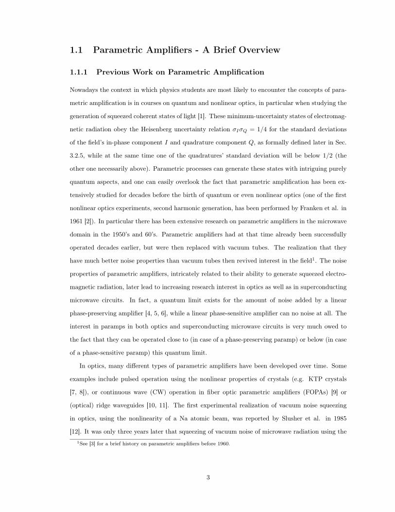
8

circuits the nonlinearities are point-like (small compared to the wavelengths involved), so that phase
matching is not an issue. Whether the device is considered frequency degenerate or non-degenerate
depends on whether signal and idler modes coincide (or at least have overlapping bandwidths). A
further distinguishing attribute is spatial degeneracy vs. non-degeneracy, i.e. whether or not signal
and idler modes are excited through the same spatial port and travel on the same transmission
line. These properties are schematically shown in Fig. 1.1, where the clear distinction between the
signal mode at frequency ωa and bandwidth γa and the applied tone at frequency ω1 is made. It
should be noted that in optics the term “non-degenerate” is often used to describe an experimental
situation where applied signal and idler waves are not at the same frequency, even though signal
and idler modes do have overlapping bandwidths, and thus the term does not refer to a property
of the paramp itself as in microwave circuits.
Josephson devices allow for the nonlinearities to be engineered to have the desired energy mixing
terms, without complications arising from spurious nonlinearities as in the case of χ(2) and χ(3)
media. Higher order nonlinear terms exist, but are usually negligible. Josephson paramps can be
grouped into three-wave mixing and four-wave mixing devices.
a) Four-Wave Mixing
Degenerate paramps based on Duffing type oscillators have been successfully built and operated
using Josephson junction arrays as nonlinear metamaterial in a coplanar waveguide (CPW) res-
onator [43, 20], or using two Josephson junctions in a direct current (DC)-SQUID configuration
(for magnetic flux tunability) as nonlinear inductance in a quasi-lumped LC-circuit [44, 45, 46, 23].
These devices have nonlinear energy mixing terms of the form X4, where X denotes the gener-
alized flux across the nonlinear inductance term of the resonant mode at ωa and bandwidth γa.
Assuming a signal tone is applied at ωa + δω, δω γa, then in this four-wave mixing interaction,
two pump photons at ωa are coherently converted into one signal photon at ωa + δω and one idler
photon at ωa − δω, as schematically shown in Fig. 1.1 b). These devices can be considered to
be doubly-degenerate in frequency, since signal, idler, and pump modes coincide. More recently,
doubly pumped operation has been achieved at Yale, with pump tones symmetrically detuned in
frequency above and below ωa [47], making the four-wave mixing nature of these devices more
obvious.
9

b) Three-Wave Mixing
An example of a singly frequency degenerate Josephson paramp is given in [22], where two Joseph-
son junctions in a DC-SQUID configuration are embedded at the voltage node of a λ/4 CPW
transmission line resonator, with resonance frequency ωa. The pump is provided by the modula-
tion at 2ωa of the flux through the SQUID loop. This degenerate three-wave mixing interaction is
described by the nonlinear mixing term X2Z, where X again is proportional to the generalized flux
across the nonlinear inductance, and Z describes the pump mode. In frequency space this amplifier
is similar to Fig. 1.1 b), with the difference that the pump is now at 2ωa.
The three above examples cover both three-wave mixing and four-wave mixing interactions, but
are all degenerate in both frequency and space, as signal and idler tones are injected through the
same ports and travel on the same transmission lines.
The JPC, on the other hand, is non-degenerate in frequency and space. It is described by a
pure three-wave mixing energy interaction term of the form XY Z, where X, Y , and Z stand for
the signal, idler, and pump modes respectively. Signal, idler, and pump modes are described by
frequencies ωa, ωb, ωc and bandwidths γa, γb, γc, with the three-wave mixing frequency relation
ωc = ωa+ωb. As schematically depicted in Fig. 1.1 a), signal tones injected withing the signal mode
bandwidth at frequency ω1 are amplified at that frequency and also converted and amplified into
idler photons at ωc − ω1, so that the three-wave mixing frequency relation still holds. In practice,
the pump is applied non-resonantly and ωc represents the pump tone frequency. This assures that
the pump is stiff, i.e. that its amplitude is much larger than signal and idler amplitudes and its
dynamics thus not affected by the signal and idler dynamics. The gain of the JPC then remains
constant over a large range of signal input powers.
1.1.3 Phase-Sensitive and Phase-Preserving Amplification
For experiments in dilution refrigerators at frequencies of several GHz, kBT ~ω and consequently,
all Johnson noise of matched loads is replaced by zero-point fluctuations. Superconducting circuits
as well as Josephson junctions are dissipation-free and full control of all modes can be achieved
while avoiding unwanted dissipation. This makes it possible for superconducting paramps to achieve
quantum-limited operation [5] and is the reason for the increasing interest the field has seen in the
past few years.
Parametric amplifiers are usually not only classified into degenerate and non-degenerate types,
10
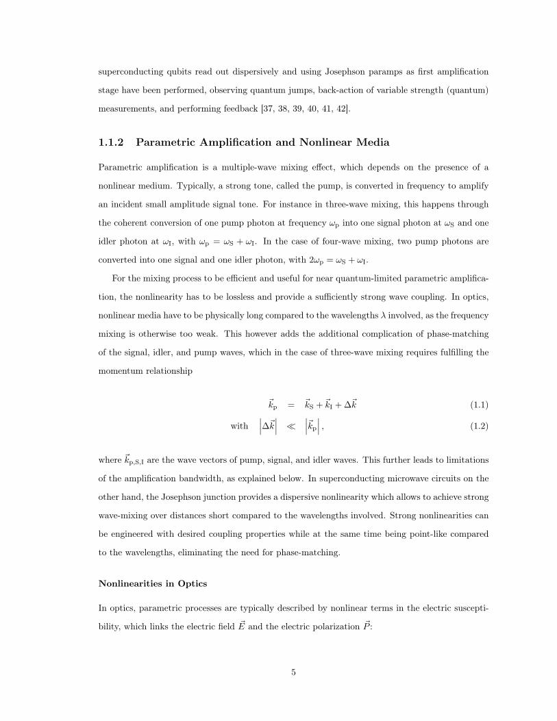
a)
I
Q
|α|
I
Qphase-preserving amp.
√G
√G•|α|
(G→∞)
√ 14+σ2
σI
σQ
I
√G √ 14+σ2
Q
I
Q
|‹Iin›|
|‹Qin›|
I
Q
σI
|‹Iin›|
|‹Qin›| σQ
σI
phase-sensitive amp. (G→∞)
2√G
1/(2√G) 2√G 1/(2√G)
b)
σQ
Figure 1.2: Fresnel vector representation of quantum-limited amplifiers. a) Phase-preserving oper-ation of a paramp such as the JPC. A coherent tone of |α|2 photons is amplified by an amplitudegain
√G and its phase is unaltered in the process. Half a photon of noise is added to the original
noise (referring the noise back to the input). b) Phase-sensitive operation, e.g. of a JBA-paramp.One quadrature (here I) is amplified by an amplitude gain 2
√G, while the other (Q) is deamplified
by the inverse (2√G)−1. The noise in the two quadratures is amplified by the same factor, so that
the signal-to-noise ratio (SNR) in each quadratures stays constant. For coherent states, σ2I,Q = 1/4.
which depends on their physical implementation, but also by whether they are operated in phase-
preserving or phase-sensitive mode. All paramps, whether optical or made of superconducting
microwave circuits, can be operated in both modes, phase-preserving and phase-sensitive. This
essentially depends on whether or not the signal to be processed is distributed over both signal and
idler. Consider for instance the case of a doubly-degenerate paramp as schematically shown in Fig.
1.1 b): applying a signal tone exactly at the center of the resonant mode at frequency ωa (or more
generally a pulse with carrier frequency ωa and frequency components symmetric about the carrier
frequency) will lead to phase sensitive amplification. In that case one can not distinguish between
signal and idler, as the signal information is distributed over and mixed into both. In case the
signal to be processed is contained on one side of ωa, the amplification process is phase-preserving
and a copy of the amplified signal will appear on the opposite side of ωa as idler.
The non-degenerate JPC is usually operated in the phase-preserving mode, as the signal to be
amplified is injected on the signal port. However it can also be operated in the phase-sensitive
mode, which is discussed detail in Chapter 5.
Figure 1.2 a) shows the operation of a phase-preserving amplifier, such as the JPC at large
11

power gains G. A signal with amplitude α is amplified with amplitude gain√G, and its phase is
the same before and after the amplification. The noise (standard deviation), represented as a disc,
grows by slightly more than√G: an energy corresponding to half a photon is added so that the
power signal-to-noise ratio (SNR) deteriorates by a factor 1 + 1/(2σ2), where for quantum-limited
signals (coherent states) σ2 = σ2I + σ2
Q = 1/2, so that the SNR is lowered by a factor of 2 in the
amplification process. Figure 1.2 b) shows the operation of a phase-sensitive amplifier, such as
the Josephson Bifurcation Amplifier (JBA)-paramp at large gains. One quadrature is amplified
by an amplitude gain 2√G, where G is the power gain in the phase-preserving operation of the
same device at the same working point, while the other quadrature is deamplified by the inverse
factor 1/(2√G). Since the noise in each quadrature is amplified/deamplified by the same respective
factors, schematically represented by the conversion of the noise disc into a noise ellipse, the overall
SNRs in each quadrature stays constant for any gain. This feature is very attractive in experiments
where the signal phase is known a priori, or where two digital outcomes, differing in phase, are of
interest, and where an offset phase is known/adjustable a priori (see e.g. [37]).
Table 1.1 classifies Josephson amplifiers developed in various research groups. Paramps are
powered by external microwave tones, while microwave SQUID amplifiers are powered with a DC
bias. The circuit properties of paramps determine whether they are of the degenerate or non-
degenerate type. Even though either can be operated in phase-sensitive or phase-preserving mode,
degenerate paramps are more easily operated in the phase-sensitive mode, while non-degenerate
paramps such as the JPC are more easily operated in the phase-preserving mode. Microwave
SQUID amplifiers on the other hand are always phase-preserving.
1.1.4 XY Z Nonlinearity and JPC Scattering Matrix
What makes the JPC stand apart from other paramps is that its Hamiltonian contains the pure
tri-linear mixing term XY Z. No other nonlinear mixing term of this order exists. When neglecting
drive and dissipation, its Hamiltonian consists of three harmonic oscillators coupled by this pure
three-wave mixing term:
12

RF Powered
DC Powered
Degenerate Non-Degenerate
Phase-
Sensitive
Boulder (“JPA”), Yale (“JBA”),
Berkeley (“JBA”), NEC, etc.
Phase-
PreservingYale (“JPC”), ENS-Paris
(“JPC”)
Berkeley, LLNL, NIST, etc.
Amplifier Type
Op
era
tio
n o
f A
mp
lifi
er
Table 1.1: Classification of Josephson amplifiers developed in various research groups. MicrowaveSQUID amplifiers are DC powered and always phase-preserving. Paramps are either of the de-generate or non-degenerate type, depending on the specific circuit, and can be operated in boththe phase-sensitive and phase-preserving mode. Non-degenerate paramps such as the JPC are usu-ally operated in the phase-preserving mode, while degenerate paramps are usually operated in thephase-sensitive mode.
13

H0 =Φ2X
2La+
Φ2Y
2Lb+
Φ2Z
2Lc(1.6)
+Q2X
2Ca+Q2Y
2Cb+Q2Z
2Cc
+KΦXΦY ΦZ ,
where ΦX,Y,Z are the generalized flux variables and QX,Y,Z their conjugate charge variables. The
three harmonic oscillators have frequencies ωa,b,c = 1/√La,b,cCa,b,c and characteristic impedances
Za,b,c0 =√La,b,c/Ca,b,c and are coupled to each other through the three-wave mixing coefficient K.
As explained in Chapter 3, under the rotating wave approximation (RWA) and for ωc = ωa + ωb
the Hamiltonian becomes
HRWA0 = ~ωaa†a+ ~ωbb†b+ ~ωcc†c+ ~g3
(a†b†c+ abc†
), (1.7)
where the three-wave mixing interaction is now described by the coupling energy ~g3 = KΦ0XΦ0
Y Φ0Z ,
where Φ0X,Y,Z :=
√⟨0∣∣∣Φ2X,Y,Z
∣∣∣ 0⟩ are the zero-point fluctuation of the flux variables. The first three
terms are simply those of three harmonic oscillators with annihilation operators a, b, c, whereas the
coupling term of the form a†b†c+ abc† can be interpreted in the following way: a†b†c describes the
annihilation of one pump photon at ωc and the creation of a pair of signal and idler photons at
ωa and ωb, respectively. This is predicted by the Manley-Rowe relations [48], which state that the
change in photon flux of signal and idler modes are equal to each other and opposite to the change
in pump photon flux: nouta − nina = noutb − ninb = ninc − noutc . It is the term a†b†c in the Hamilitonian
which gives rise to parametric amplification. The hermitian conjugate term abc† describes the
reverse process: a pair of signal and idler photons are annihilated to create one pump photon.
For balanced signal and idler inputs and with the correct phase relation between signal, idler, and
pump, this other process leads to Coherent Attenuation (CA), which is discussed in Chapter 5.
As explained in Ch. 3, under the stiff pump approximation and for incoming and outgoing
signal and idler tones at zero detuning, i.e. at ω1 = ωa and ω2 = ωb, Eq. 1.7 leads to the two-port
14
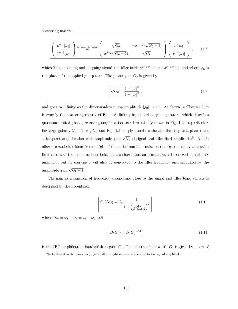
scattering matrix
aout[ω1]
bout†[ω2]
ω1=ωa; ω2=ωb=
√G0 −ie−iϕp
√G0 − 1)
ieiϕp√G0 − 1)
√G0
ain[ω1]
bin†[ω2]
, (1.8)
which links incoming and outgoing signal and idler fields ain/out[ω] and bin/out[ω], and where ϕp is
the phase of the applied pump tone. The power gain G0 is given by
√G0 =
1 + |ρ0|2
1− |ρ0|2, (1.9)
and goes to infinity as the dimensionless pump amplitude |ρ0| → 1−. As shown in Chapter 3, it
is exactly the scattering matrix of Eq. 1.8, linking input and output operators, which describes
quantum-limited phase-preserving amplification, as schematically shown in Fig. 1.2. In particular,
for large gains√G0 − 1 ≈
√G0 and Eq. 1.8 simply describes the addition (up to a phase) and
subsequent amplification with amplitude gain√G0 of signal and idler field amplitudes5. And it
allows to explicitly identify the origin of the added amplifier noise on the signal output: zero-point
fluctuations of the incoming idler field. It also shows that an injected signal tone will be not only
amplified, but its conjugate will also be converted to the idler frequency and amplified by the
amplitude gain√G0 − 1.
The gain as a function of frequency around and close to the signal and idler band centers is
described by the Lorentzian:
G0(∆ω) = G01
1 +(
∆ωB(G0)/2
)2 , (1.10)
where ∆ω = ω1 − ωa = ωb − ω2 and
B(G0) = B0G−1/20 (1.11)
is the JPC amplification bandwidth at gain G0. The constant bandwidth B0 is given by a sort of5Note that it is the phase conjugated idler amplitude which is added to the signal amplitude.
15
average of the signal and idler mode bandwidths γa, γb through
B0 =2γaγbγa + γb
. (1.12)
Figure 1.1 a) schematically shows the two Lorentzian gain response functions centered around the
signal and idler mode frequencies ωa, ωb. An applied and amplified signal tone at ω1 is shown as
solid arrow, and the resulting idler tone at ω2 = ωc − ω1 as dashed arrow.
1.2 A Practical Parametric Amplifier Based on the Josephson
Ring Modulator
The goal of this thesis work was to build and operate a practical quantum-limited, non-degenerate
and phase-preserving parametric amplifier at microwave frequencies based on the XY Z nonlin-
earity described above. This means that the amplifier needs to be useful when inserted into the
measurement chain of an experiment, and not simply be a proof-of-concept device. In particular,
the amplifier needs to noticeably reduce the system noise temperature by not only having a lower
noise temperature than the following stage amplifier, but also by having sufficient gain. At the
same time the device needs to have sufficient bandwidth and the capability to operate at large
enough input powers. A practical amplifier should further either have a very large bandwidth, or
be frequency tunable over a sufficiently large range. Paramps are rather high Q devices, making
frequency tunability crucial to match the amplifier center frequency to the measurement frequency.
As explained in this section, the JPC amplifier developed in this work fulfills those requirements and
can be used in the readout of the state of superconducting qubits. The qubit architecture of choice
in our group at Yale is circuit quantum electrodynamics (cQED), where a microwave resonator is
used to manipulate and measure the state of a qubit [49, 50, 51]. Similar to the case of an atom
in a cavity [52, 53], superconducting qubit and resonator exchange energy so that the qubit state
encoded in the resonator microwave field can be dispersively measured by monitoring this field,
leading to a quantum non-demolition (QND) measurement. For a preamplifier such as the JPC to
be useful in such a measurement scheme, several requirements have to be met.
16

1.2.1 Paramp Requirements
Commercially available cryogenic HEMT amplifiers [54] have noise temperatures typically corre-
sponding to 10-20 added photons at frequencies of 1-12 GHz. The most obvious requirement for
a paramp preamplifier sitting between qubit readout resonator and HEMT amplifier is for it to
have a significantly lower noise temperature and enough gain at the readout frequency, in order to
reduce the combined system noise temperature. This noise temperature should ideally approach
the standard quantum limit of half a photon of added noise, and allows for instance monitor the
qubit state in real-time through partial (non-projective) measurements [37, 42] and to implement
feedback loops [40, 38, 41].
With a JPC in the measurement chain, the system noise temperature is given by
T sysN =
1
GJPCTHEMTN + T JPC
N , (1.13)
where the gain GJPC is the JPC gain including possible losses between qubit and JPC, THEMTN is
the HEMT noise temperature including possible losses before the HEMT, and T JPCN is the JPC
noise temperature, including possible losses between qubit and JPC. This expression shows that
it is not sufficient for the JPC to operate at the quantum limit of TQ = ~ω/2kB corresponding to
half a photon of added noise, but that it also needs to exhibit sufficient gain to lead to a significant
improvement of the SNR of the system.
A further requirement is that the JPC has a sufficiently large dynamical 3dB amplification
bandwidth B, in the range B/2π = 1 − 10MHz, and which corresponds to a signal processing
time (or more exactly: cavity rise time) of 160 − 16 ns. The transmon [55, 56, 57] and fluxonium
[58] qubits pioneered at Yale nowadays routinely achieve lifetimes of the order of one hundred
microseconds [59] and have readout cavities with bandwidths in the 1 − 10MHz range [60]. But
even for qubit lifetimes T1 of a few microseconds, a JPC dynamical bandwidth of order 1− 10MHz
allows to extract many bits of information per T1 even when measuring with few photons. The JPC
also needs to be able to handle the powers with which qubits are measured. In QND schemes this
power typically corresponds to a few photons per readout cavity lifetime at the readout frequency.
In terms of ease of operation, the JPC center frequency needs to be tunable over at least 100
MHz, to make it easy to match JPC and qubit readout frequencies. Lastly, a flexible and simple
sample fabrication process is desirable.
17

Characteristic Desired Achievedωa,b/2π 5− 12 GHz 5− 8.5 GHz
dynamical BW B/2π 1− 10 MHz 3− 10 MHzGmax ≥ 20 dB ≥ 20 dB
frequency tunability 100 MHz ≥ 400 MHzkBTN/~ωa 1
2 . 2− 3PmaxSig /~ωaB ≥ 1 @ 20 dB 1− 10 @ 20 dB
out-of-band backaction negligible none observed
Table 1.2: Desirable preamplifier characteristics and values typically achieved with the JPC in thiswork.
Φext
a) b)1
2
34
1
2
34
Figure 1.3: Schematic of the Josephson Ring Modulator (JRM). a) Unshunted JRM with fourJosephson junctions (red). b) Shunted JRM with four additional shunt junctions (yellow).
Table 1.2 summarizes requirements to a preamplifier for qubit readout and shows typical values
achieved with the JPC in this work. Devices were designed to typically have signal and idler
frequencies around 8 GHz and 5−6 GHz, with linear bandwidths γa,b/2π of up to 100 MHz. Gains
of above 20 dB were routinely achieved (see Table 4.1 in Ch. 4).
1.2.2 The Josephson Ring Modulator
The circuit element used to achieve a pure three-wave mixing nonlinearity of the tri-linear form
XY Z is the JRM, which consists, in its simplest form, of a ring of four nominally identical Josephson
junctions, as shown in Fig. 1.3 a). The JRM is inspired by the diode ring modulator as used in
double balanced microwave mixers [61] and which perform a similar (but lossy) frequency conversion
scheme to that of the JPC.
As explained in Chapter 2, this (unshunted) JRM is well described by the approximate energy
expression
18

E4JJJRM
ϕX,Y,Z1= −EJ sin
(ϕext4
+ nπ
2
)ϕXϕY ϕZ + EJ cos
(ϕext4
+ nπ
2
)(ϕ2X
2+ϕ2Y
2+ 2ϕ2
Z − 4
),
(1.14)
where EJ is the Josephson energy, ϕext is the reduced applied magnetic flux through the ring,
n = 0, 1, 2, 3, and ϕX,Y,Z are reduced generalized fluxes of modes X,Y, Z. In terms of generalized
node fluxes φi ≡´ t−∞ vi(t
′)dt′ at nodes i = 1, 2, 3, 4, where vi is the electric potential at node i,
these modes can be expressed as
ϕXJRM= ϕ−1
0 (φ3 − φ4) (1.15)
ϕYJRM= ϕ−1
0 (φ1 − φ2) (1.16)
ϕZJRM= ϕ−1
0
(φ1 + φ2 − φ3 − φ4
2
), (1.17)
where ϕ0 ≡ ~/2e is the reduced magnetic flux quantum. Thus X represents a differential
excitation across nodes 3 and 4, Y represents a differential excitation across nodes 1 and 2, and Z
corresponds to a differential excitation with a gradient in flux between nodes 1, 2 and 3, 4.
The first term in Eq. 1.14 is the desired XY Z coupling term, maximized at ϕext = 2π. The
system has four solutions n = 0, 1, 2, 3 for a given applied magnetic flux, leading to different values
of the coupling strength −EJ sin(ϕext
4 + nπ2). The state n of the system depends on the history
of the magnetic flux ϕext and jumps between these states can occur, so that in practice the device
is operated at ϕext = π (i.e. Φext = Φ0/2), as explained in more detail in Ch. 2. The second
term in Eq. 1.14 is quadratic in ϕX,Y,Z , only renormalizing the mode frequencies. The prefactor
EJ cos(ϕext
4 + nπ2)suggests that the mode frequencies can be tuned with the external magnetic flux
ϕext, but in practice this tunability is severely limited by the fact that jumps can occur between
the different states n.
By quartering the ring with four additional larger junctions (Fig. 1.3 b)), which behave like
linear inductors, tunability over a large frequency range can be achieved. In this case, the device
becomes frequency tunable over the range ϕext ∈ [0, ϕcrossoverext ], where ϕcrossoverext is given by the
solution of −4βL cos(ϕcrossoverext /4) = 1, or by 2π if no solution exists. Here, βL is the ratio between
the Josephson energy EJ of the smaller outer Josephson junction and the Josephson energy EshuntJ
19
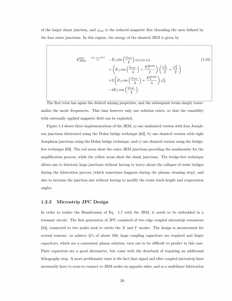
of the larger shunt junction, and ϕext is the reduced magnetic flux threading the area defined by
the four outer junctions. In this regime, the energy of the shunted JRM is given by
E8JJJRM
ϕX,Y,Z1= −EJ sin
(ϕext4
)ϕXϕY ϕZ (1.18)
+
(EJ cos
(ϕext4
)+EshuntJ
2
)(ϕ2X
2+ϕ2Y
2
)+2
(EJ cos
(ϕext4
)+EshuntJ
4
)ϕ2Z
−4EJ cos(ϕext
4
).
The first term has again the desired mixing properties, and the subsequent terms simply renor-
malize the mode frequencies. This time however only one solution exists, so that the tunability
with externally applied magnetic field can be exploited.
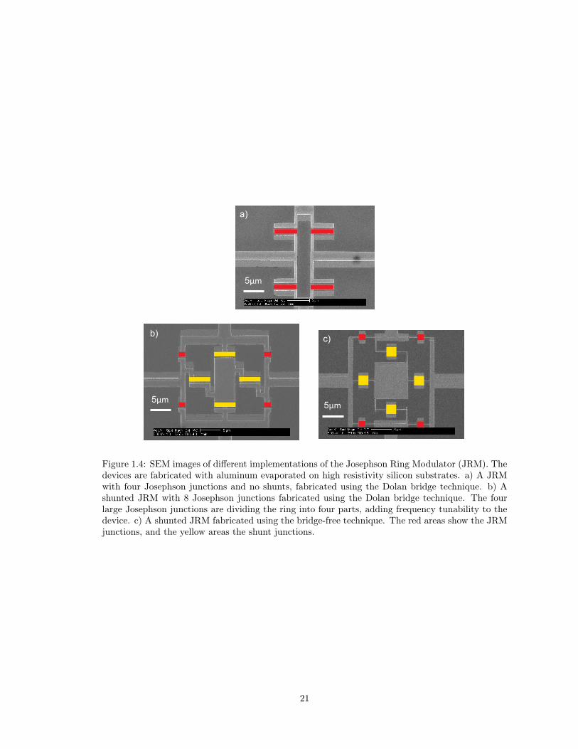
Figure 1.4 shows three implementations of the JRM, a) one unshunted version with four Joseph-
son junctions fabricated using the Dolan bridge technique [62], b) one shunted version with eight
Josephson junctions using the Dolan bridge technique, and c) one shunted version using the bridge-
free technique [63]. The red areas show the outer JRM junctions providing the nonlinearity for the
amplification process, while the yellow areas show the shunt junctions. The bridge-free technique
allows one to fabricate large junctions without having to worry about the collapse of resist bridges
during the fabrication process (which sometimes happens during the plasma cleaning step), and
also to increase the junction size without having to modify the resist stack height and evaporation
angles.
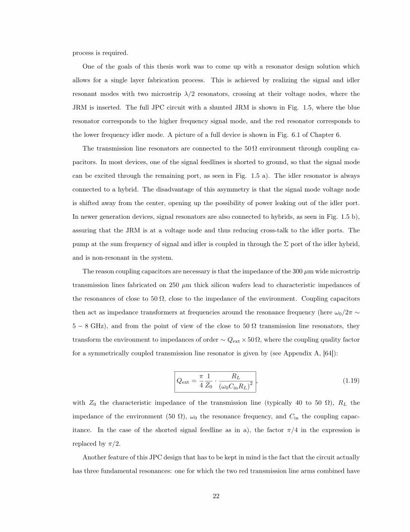
1.2.3 Microstrip JPC Design
In order to realize the Hamiltonian of Eq. 1.7 with the JRM, it needs to be embedded in a
resonant circuit. The first generation of JPC consisted of two edge coupled microstrip resonators
[24], connected to two nodes each to excite the X and Y modes. The design is inconvenient for
several reasons: to achieve Q’s of about 100, large coupling capacitors are required and finger
capacitors, which are a convenient planar solution, turn out to be difficult to predict in this case.
Plate capacitors are a good alternative, but come with the drawback of requiring an additional
lithography step. A more problematic issue is the fact that signal and idler coupled microstrip lines
necessarily have to cross to connect to JRM nodes on opposite sides, and so a multilayer fabrication
20
5μm
a)
5μm
b)
5μm
c)
Figure 1.4: SEM images of different implementations of the Josephson Ring Modulator (JRM). Thedevices are fabricated with aluminum evaporated on high resistivity silicon substrates. a) A JRMwith four Josephson junctions and no shunts, fabricated using the Dolan bridge technique. b) Ashunted JRM with 8 Josephson junctions fabricated using the Dolan bridge technique. The fourlarge Josephson junctions are dividing the ring into four parts, adding frequency tunability to thedevice. c) A shunted JRM fabricated using the bridge-free technique. The red areas show the JRMjunctions, and the yellow areas the shunt junctions.
21
process is required.
One of the goals of this thesis work was to come up with a resonator design solution which
allows for a single layer fabrication process. This is achieved by realizing the signal and idler
resonant modes with two microstrip λ/2 resonators, crossing at their voltage nodes, where the
JRM is inserted. The full JPC circuit with a shunted JRM is shown in Fig. 1.5, where the blue
resonator corresponds to the higher frequency signal mode, and the red resonator corresponds to
the lower frequency idler mode. A picture of a full device is shown in Fig. 6.1 of Chapter 6.
The transmission line resonators are connected to the 50 Ω environment through coupling ca-
pacitors. In most devices, one of the signal feedlines is shorted to ground, so that the signal mode
can be excited through the remaining port, as seen in Fig. 1.5 a). The idler resonator is always
connected to a hybrid. The disadvantage of this asymmetry is that the signal mode voltage node
is shifted away from the center, opening up the possibility of power leaking out of the idler port.
In newer generation devices, signal resonators are also connected to hybrids, as seen in Fig. 1.5 b),
assuring that the JRM is at a voltage node and thus reducing cross-talk to the idler ports. The
pump at the sum frequency of signal and idler is coupled in through the Σ port of the idler hybrid,
and is non-resonant in the system.
The reason coupling capacitors are necessary is that the impedance of the 300 µmwide microstrip
transmission lines fabricated on 250 µm thick silicon wafers lead to characteristic impedances of
the resonances of close to 50 Ω, close to the impedance of the environment. Coupling capacitors
then act as impedance transformers at frequencies around the resonance frequency (here ω0/2π ∼
5 − 8 GHz), and from the point of view of the close to 50 Ω transmission line resonators, they
transform the environment to impedances of order ∼ Qext×50 Ω, where the coupling quality factor
for a symmetrically coupled transmission line resonator is given by (see Appendix A, [64]):
Qext =π
4
1
Z0· RL
(ω0CinRL)2 , (1.19)
with Z0 the characteristic impedance of the transmission line (typically 40 to 50 Ω), RL the
impedance of the environment (50 Ω), ω0 the resonance frequency, and Cin the coupling capac-
itance. In the case of the shorted signal feedline as in a), the factor π/4 in the expression is
replaced by π/2.
Another feature of this JPC design that has to be kept in mind is the fact that the circuit actually
has three fundamental resonances: one for which the two red transmission line arms combined have
22
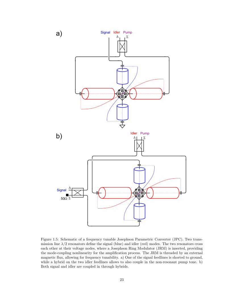
Signal Idler Pump∆ Σ
a)
50Ω
Signal
Idler Pump∆
Σ
Σ
∆
b)
Figure 1.5: Schematic of a frequency tunable Josephson Parametric Converter (JPC). Two trans-mission line λ/2 resonators define the signal (blue) and idler (red) modes. The two resonators crosseach other at their voltage nodes, where a Josephson Ring Modulator (JRM) is inserted, providingthe mode-coupling nonlinearity for the amplification process. The JRM is threaded by an externalmagnetic flux, allowing for frequency tunability. a) One of the signal feedlines is shorted to ground,while a hybrid on the two idler feedlines allows to also couple in the non-resonant pump tone. b)Both signal and idler are coupled in through hybrids.
23
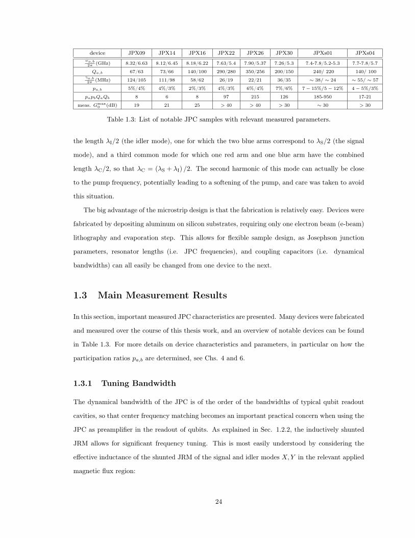
device JPX09 JPX14 JPX16 JPX22 JPX26 JPX30 JPXs01 JPXs04ωa,b2π (GHz) 8.32/6.63 8.12/6.45 8.18/6.22 7.63/5.4 7.90/5.37 7.26/5.3 7.4-7.8/5.2-5.3 7.7-7.8/5.7
Qa,b 67/63 73/66 140/100 290/280 350/256 200/150 240/ 220 140/ 100γa,b2π (MHz) 124/105 111/98 58/62 26/19 22/21 36/35 ∼ 38/ ∼ 24 ∼ 55/ ∼ 57
pa,b 5%/4% 4%/3% 2%/3% 4%/3% 6%/4% 7%/6% 7− 15%/5− 12% 4− 5%/3%
papbQaQb 8 6 8 97 215 126 185-950 17-21
meas. Gmax0 (dB) 19 21 25 > 40 > 40 > 30 ∼ 30 > 30
Table 1.3: List of notable JPC samples with relevant measured parameters.
the length λI/2 (the idler mode), one for which the two blue arms correspond to λS/2 (the signal
mode), and a third common mode for which one red arm and one blue arm have the combined
length λC/2, so that λC = (λS + λI) /2. The second harmonic of this mode can actually be close
to the pump frequency, potentially leading to a softening of the pump, and care was taken to avoid
this situation.
The big advantage of the microstrip design is that the fabrication is relatively easy. Devices were
fabricated by depositing aluminum on silicon substrates, requiring only one electron beam (e-beam)
lithography and evaporation step. This allows for flexible sample design, as Josephson junction
parameters, resonator lengths (i.e. JPC frequencies), and coupling capacitors (i.e. dynamical
bandwidths) can all easily be changed from one device to the next.
1.3 Main Measurement Results
In this section, important measured JPC characteristics are presented. Many devices were fabricated
and measured over the course of this thesis work, and an overview of notable devices can be found
in Table 1.3. For more details on device characteristics and parameters, in particular on how the
participation ratios pa,b are determined, see Chs. 4 and 6.
1.3.1 Tuning Bandwidth
The dynamical bandwidth of the JPC is of the order of the bandwidths of typical qubit readout
cavities, so that center frequency matching becomes an important practical concern when using the
JPC as preamplifier in the readout of qubits. As explained in Sec. 1.2.2, the inductively shunted
JRM allows for significant frequency tuning. This is most easily understood by considering the
effective inductance of the shunted JRM of the signal and idler modes X,Y in the relevant applied
magnetic flux region:
24

7.8
7.6
7.4
7.2
7.0JPC
Fre
quen
cy (G
Hz)
-1 0 1Φext/Φ0
Figure 1.6: Measured JPC signal frequency as a function of the externally applied magnetic fluxthreading a shunted JRM (sample JPXs01). The flux is expressed in number of flux quanta Φ0 =h/2e and refers to the area enclosed by the outer loop. The colored lines correspond to the datashown in Fig. 1.7. Similar results have been obtained in [28].
L−1X,Y
ϕX,Y,Z1=
(LshuntJ
)−1
2
(2βL cos
(ϕext4
)+ 1), (1.20)
where βL = EJ/EshuntJ , and Lshunt
J is the Josephson inductance of the shunt junctions. For βL large
enough, there exist external magnetic fluxes such that the term 2βL cos(ϕext
4
)+ 1 becomes small
and thus the effective JRM inductance large, pulling the frequency down. This behavior is shown
in Fig. 1.6, where the measured JPC signal center frequency as a function of applied magnetic flux
around zero is shown. The linear signal frequency can be tuned by close to 1 GHz, compared to
only tens of MHz typically achieved by detuning the pump frequency with a four junction JRM.
The colored lines in the figure indicate the flux bias points at which gain was measured, when
applying a pump tone at the sum of signal and idler frequencies (13.1 to 12.5 GHz) with the
appropriate powers. The measured Lorentzian-like power gain response functions are shown in Fig.
1.7. The gains of 20 dB were chosen only as reference; maximum gains achieved for this device
were ∼ 30 dB. The photon flux at which the JPC saturates at this gain depends on the biasing
point. The numbers next to the gain curves correspond to the measured saturation photon flux
per dynamical bandwidth at those points (B ≈ 2π · 3MHz). The data of the saturation photon
numbers presented here are to be understood as a proof of principle only. Those numbers can be
maximized by carefully choosing the flux bias and pump frequency, and differences of up to 10 dB
in the saturation powers for the same gain and center frequency have been observed. Newer devices
25

20
15
10
5
0G
ain
(dB
)7.807.707.607.507.40
Frequency (GHz)
120.520.30.1
Figure 1.7: Measured Lorentzian gain response functions of a JPC with inductively shunted JRM(sample JPXs01) for different magnetic flux bias points. Bias points are shown in Fig.1.6. Similarresults have been obtained in [28]. Numbers represent saturation photon numbers at those gainpoints. Note that the operating points shown here were not optimized to give the largest possiblesaturation photon numbers, but rather chosen as a proof of principle, as explained in the text. Morerecent devices fabricated in our group are able to routinely process 10 photons or more [65].
measured while this thesis was written appear to have better saturation powers for similar gains
and bandwidths, and saturation powers generally about 10 dB larger than those shown here have
been reported in [28].
1.3.2 Gain and Dynamical Bandwidth
The gain of the JPC depends on the pump power applied. As the normalized pump amplitude
|ρ0| → 1−, the gain G0 at the JPC center increases, as explained in Sec. 1.1.4. At the same time,
the dynamical bandwidth reduces as G−1/20 , so that the amplitude-gain-bandwidth product B×G1/2
0
is constant and equal to B0 = 2γaγb/(γa + γb), where γa,b is the linear signal/idler bandwidth.
Figure 1.8 a) shows the measured gain response function of a JPC with a four junction JRM.
The gain curves all lie on top of each other, but the 3 dB bandwidth reduces with increasing gain,
from about 28 MHz at a gain of 9 dB to about 9 MHz a gain of 19 dB. The white trace on top of
the red trace is a Lorentzian fit to the 0 dB pump power trace. Figure 1.8 shows the bandwidth
of the same data as a function of the inverse amplitude gain together with a line fit. The fit gives
an amplitude-gain-bandwidth product of 80 MHz, which is close to the expected value of 100 MHz
from the measured signal and idler linear bandwidths.
26

3025201510B
andw
idth
(MH
z)
0.350.300.250.200.150.10
G-1/2 (linear)
101214161820G (dB)
data line fit
20
16
12
8
4
0
Gai
n (d
B)
8.168.148.128.108.088.068.048.02Frequency (GHz)
Pump power 0 dB
-0.10 dB -0.23 dB -0.29 dB -0.59 dB -0.89 dB -1.33 dB -1.74 dB
a)
b)
Lorentzian fit
Figure 1.8: Gain and dynamical bandwidth of a JPC (sample JPX14). a) Measured power gainresponse function as a function of frequency. The maximum gain increases from 5 dB to 19 dB withincreasing applied pump power (purple to red). Note that the applied pump power is changed byless than 60% (2 dB). A Lorentzian fit to the 0 dB pump data is shown as white trace. b) 3 dBbandwidth as a function of maximum gain. The bandwidth increases linearly with the inverse ofthe amplitude gain.
1.3.3 Gain and Power Limitations
The previous discussion about dynamical JPC bandwidth seems to suggest that the linear resonator
bandwidths need to simply be increased in order to achieve more amplifier bandwidth, and so the
question arises why the coupling capacitors are necessary at all in the presented microstrip design.
In fact, there are several more limitations on the power and gain of the JPC, which require the
linear resonator quality factors Qa,b = ωa,b/γa,b to be sufficiently large. The limitations on the
gain, power, and bandwidth are ultimately determined by the Josephson energy EJ made available
by the junctions, the frequency ωa,b at which the device is operated, and the participation ratios
pa,b of the JRM inductance compared to resonant circuit inductance, as defined later in Sec. 3.1.
The following mechanisms restrict the maximum gains and powers the JPC can handle [25, 27]:
1. The signal power is too large and excites higher order nonlinearities.
In the derivation of the JRM energy (Eqs. 1.14, 1.18), it is assumed that the generalized fluxes
ΦX,Y remain small compared to Φ0, so that the expansion to only third order remains valid.
Or, using the particle analogy commonly used in the description of Josephson junctions, it
means that the position ΦX,Y needs be small enough so that the particle remains close to
27
the bottom of the potential well. This requires the maximum power in the signal (and idler)
resonator to remain finite, and the limit is given by
Pmaxcav =
γa,bpa,b
EeffJ , (1.21)
where EeffJ is an effective Josephson energy available for the amplification process. This
maximum power is to be understood as the maximum power the JPC can provide at the
output of signal and idler ports. This suggests that large junctions, small participation ratios,
and large bandwidths are desirable.
2. The pump power is too large and excites higher order nonlinearities.
In this case, the pump power can never reach the limit |ρ0| → 1−, required to achieve appre-
ciable gains (Eq. 1.9), without excitation of higher order nonlinear terms. To assure that high
gains are possible, the circuit needs to designed such that the Q · p−product is large enough,
QaQbpapb > Ξ, (1.22)
where Ξ is a number of order unity [27]. In practice (see Table 4.1) it was observed that
a Q · p−product smaller than 10 leads to maximum gains of 20 dB and below, whereas a
Q · p−product larger than 10, gains of above 30 dB were routinely achieved. A second effect
observed with samples of small Q · p−product is that the gain abruptly drops once the signal
input power becomes too large [26]. Thus, for large bandwidth (small Q’s), large participation
ratios are required.
3. The signal photon flux becomes comparable to the pump photon flux.
The two requirements above are still met, i.e. ΦX,Y,Z Φ0 is still true, large gains can be
achieved, and the power circulating in the signal resonator is easily handled by the junctions,
and the three-wave mixing term in the Hamiltonian fully describes the system. However, the
stiff pump approximation, which says the dynamics of the pump can be neglected, is not true
anymore. In this case, the fully nonlinear regime is reached and signal, idler, and pump modes
are to be treated on the same footing, as described by the three coupled nonlinear equations
of motion presented in Chapter 3 (Eq. 3.5). The consequence is that when the signal input
photon flux is increased, the gain G will eventually drop to 1− ε of its original value G0. For
28
this drop not to exceed 1− ε, the following condition has to be met:
x < 2εG−3/20 , (1.23)
where x ≡ na/nc is the ratio between signal and pump photon fluxes (the signal and pump
power is given by Pa,c = ~ωa,cna,c). This expression predicts for instance that at the operating
point G0 = 20dB, the gain will drop by 1dB (ε ≈ 0.2) when the signal photon flux na is about
34 dB lower than the pump photon flux, but says nothing about the absolute photon fluxes.
These absolute photon fluxes are determined by noting that, at high gains, the pump photon
flux is close to the threshold photon flux equivalent to |ρ0| ≈ 1−, nc ≈ npoc = γaγbγc/4g23 ,
and g23/~ = papbpcωaωbωc/E
eff?J , where Eeff?
J ∝ EJ with a numerical prefactor. So one finally
arrives at the condition for the incoming signal photon flux not to lead to the softening of the
pump with associated drop in gain (by 1− ε):
na < 2εG−3/20 × npoc = 2εG
−3/20 × 1
QaQbpapb· γc
4pcωc· Eeff?
J /~ (1.24)
4. Amplified zero-point fluctuations become too large for junctions.
The JPC signal and idler resonator always have to amplify zero-point fluctuations, and this
circulating power in the resonators, can overwhelm the junctions for too large gains. This
sets the limit of the maximum gain achievable to
GmaxZPF = Eeff
J
2
~ωa,bpa,b, (1.25)
where again EeffJ is the effectively available junction energy. Large junctions and small par-
ticipation ratios are favorable in this case.
Equations 1.11,1.12,1.21,1.22,1.24, and 1.25 thus show that it is not possible to simultaneously
optimize for gain, bandwidth, and input power handled by the JPC, and compromises need to be
made. The bandwidths typically achieved here of 3− 10 MHz at gains of 20 dB with participation
ratios of a few percent allow to achieve saturation input powers of a few photons. It should be
possible to even further increase the JPC dynamical bandwidth and saturation powers in future
generation devices, by increasing the linear bandwidths and Josephson junction size while at the
same time increasing the participation ratio.
29

-165
-155
-145
-135
-125
-115
-105
-95
P out
(dB
m)
-165 -155 -145 -135 -125 -115 -105
Pin (dBm)
Gain G0 28 dB 24 dB 19 dB 16 dB 10 dB
1 photon @ 5 MHz
30
25
20
15
10
5
0
Gai
n (d
B)
-165 -155 -145 -135 -125 -115 -105
Pin (dBm)
GZPF
max
GZPF
max
1 photon @ B0G-1/20
Pcavmax
Pcavmax
a) b)
Figure 1.9: Measured JPC gain and output power dependence as a function of signal input powers(sample JPXs01). a) The gain is constant for small input powers and drops at larger powers. Thedashed lines represent the expected maximum gain, maximum power (see text), and the powerrepresenting one photon at the bandwidth B = B0G
−1/2. b) Same data as a), plotted as outputpower G0Pin. The dashed line referring to the one photon input power is with respect to a constantbandwidth of 5 MHz. Device parameters: pa = 0.1, I0 = 1µA (EJ/h = 496GHz.), γa ≈ B0 =2π × 31 MHz, ωa = 2π × 7.6 GHz, papbQaQb ∼ 102 (Eeff
J = EJ/√
2 chosen [27]).
30

Figure 1.9 a) shows how the measured gain of a JPC depends on the signal input power, and
the discussed expected limitations are drawn as dashed lines for the parameters of this device
(see caption text and Table 4.1). This device has a Q · p−product of several hundred, so that
large gains (∼ 30 dB) can be easily achieved. This device can handle about 1 photon at gains
of 20 dB, as indicated by a dashed line, and shows constant gains G0 for input powers below the
saturation powers. Note that the calculated GmaxZPF is also around 30 dB, where it was assumed
that EeffJ = EJ/
√2 [26]. It is likely that the estimations of Eeff
J and pa for this particular device
were not accurate, as one should not expect to be able to operate too close to GmaxZPF. Figure 1.9
b) shows the same data as in a), but plotted as output power vs. input power. Even though the
calculated maximum output power Pmaxcav = −94 dB is clearly above the maximum power achieved
by this device, the device appears to be limited by an effective maximum output power about 10dB
lower when saturating. This suggests that the relevant saturation mechanism here is either that
a maximum circulating power in the signal resonator has been reached, or that the signal photon
flux starts to become large compared to the idler photon flux.
1.3.4 SNR Improvement
Adding a JPC in a measurement chain as preamplifier to a HEMT amplifier leads to a decrease
of the measurement system noise temperature. In principle, the JPC adds only half a photon of
noise if operated in the low temperature regime kBT ~ω. To date, reported measurements of
the JPC noise temperature set an upper bound at about 1.5 to 2 added photons [66, 28]. What
is more important to the experimenter than the measured or inferred noise temperature however,
is to verify that the JPC in the measurement chain actually improves the overall system noise
performance compared to the case where the JPC is absent. This change in the system properties
then also reflects possible losses from cryogenic circulators, transmission lines connecting the various
components, connectors, etc..
The ratio between the system noise temperature with and without JPC in the measurement
chain is the noise rise, given by
noise rise =GJPC · T JPC sys
N + THEMT sysN
THEMT sysN
(1.26)
and the improvement of the SNR due to the JPC can then be expressed as the ratio of the JPC
31

14
12
10
8
6
4
2
0S
NR
impr
ovem
ent (
dB)
2520151050Gain (dB)
data fit
Figure 1.10: Signal-to-noise ratio improvement with JPC in measurement chain (JPXs01). At lowJPC gain, the system noise is dominated by the HEMT amplifier noise, while at large JPC gain itis dominated by the JPC noise.
gain to the noise rise:
SNR impr. =GJPC
noise rise(1.27)
=GJPC(
GJPC · T JPC sysN + THEMT sys
N
)/THEMT sys
N
(1.28)
=1
T JPC sysN /THEMT sys
N + 1/GJPC, (1.29)
where T JPC sysN and THEMT sys
N refer to the effective noise temperatures of the JPC and HEMT,
taking into account the imperfections of the setup. As expected, this expression predicts that for
small JPC gain the SNR improvement increases linearly as GJPC, since the noise at the JPC output
GJPC ·T JPC sysN is small compared to THEMT sys
N . Note that commercially available HEMT amplifiers
nowadays have noise temperatures of 4 K at 8 GHz, but taking into account the setup, system
noise temperatures of 10 K are more realistically achieved. At the same time, the noise temperature
of half a photon, TQ, at 8 GHz is about 190 mK. On the other hand, at large JPC gains, Eq. 1.29
shows that the SNR improvement saturates at the ratio of the HEMT noise temperature to the
JPC noise temperature.
Figure 1.10 shows the measured SNR improvement on the signal port as a function of JPC gain
for a sample with shunted JRM. The gain was measured with a small amplitude probe tone at
32

the amplification center frequency of 7.64 GHz and in a 10 Hz bandwidth. The probe power was
reduced with increasing gain, to ensure not to saturate the device. The noise rise was measured at
the center frequency in a 1 kHz bandwidth, which is much smaller than the dynamical bandwidth of
this device of 3 MHz at 20 dB of gain. The SNR improvement shown must thus be understood as an
ideal value, which is reduced when the signal to be processed is making use of the entire dynamical
bandwidth available. The dashed lines show the behavior in the limiting cases of low and high
gains. The fit function (black line) has only one free fit parameter, the ratio T JPC sysN /THEMT sys
N ,
which is found to be −11.4 dB (equal to the negative of the dashed constant line). Assuming a
system noise temperature of 10 K with only the HEMT, this implies an added noise of 2 photons
(720 mK) of the system consisting of the JPC sample at the given bias point and embedded in the
measurement chain, consistent with previous results.
1.3.5 Qubit Measurements
The frequency tunable JPCs developed in the course of this thesis work are now routinely used
in the readout of superconducting transmon [57, 59] and fluxonium [58] qubits. The dispersive
readout scheme consists of monitoring coherent states injected at the readout cavity frequency for
the measurement time Tm. The qubits interact with the field in the cavity, so that its state is
ultimately mapped onto the state of the itinerant microwave field [50].
Figure 1.11 shows measured microwave field quadrature histograms obtained in the dispersive
readout of a transmon qubit6[42]. The quantum state of the qubit is mapped onto the phase of
the coherent states injected at the cavity frequency of 7.541GHz. By rotating the I − Q plane
appropriately, all qubit state information is contained in the Im quadrature, where Im is the in-
phase quadrature of the measured field (here in uncalibrated units). As is clearly visible, using
a JPC amplifier considerably improves the ability to discriminate between the qubit population
being in the ground vs. the excited state, leading to a separation of the two Gaussian histograms
of almost 5σ. In particular, it reveals that even without an excitation pulse, the qubit has 8%
of its population in the excited state (small blue hump), corresponding to a qubit temperature of
∼ 100mK.
This increased discrimination capability for instance makes it possible for the qubit state to be
monitored in real time, revealing quantum jumps between the ground and the excited state [37, 42].6Qubit measurements presented here were performed by S. Shankar and M. Hatridge.
33

150
100
50
0
Cou
nts
(x10
3 )
-4 0 4Im
400
300
200
100
0
Counts (x10
3) no pulseπ-pulse JPC on
JPC off
Figure 1.11: Transmon qubit measured with (solid lines) and without (dashed lines) a JPC(JPXs01), tuned to the qubit readout frequency of 7.541GHz. The dynamical bandwidth at thegain of 13 dB is 6MHz, greater than the readout cavity bandwidth of 5.5MHz. The readout powercorresponds to 5 photons in the readout cavity. A measurement of Im = ±2 corresponds to thequbit most likely being in the excited/ground state. Gaussian histograms are separated by almost5σ when measured with JPC. (Data courtesy of S. Shankar and M. Hatridge.)
Im
Time (µs)2 4 6 8
2
-2
0
Figure 1.12: Quantum jumps of a transmon qubit measured with a JPC (JPXs01). (Data courtesyof S. Shankar and M. Hatridge.)
34
Figure 1.12 shows quantum jumps measured in the same device of Fig. 1.11, where the measurement
time Tm = 240 ns is short compared to the qubit lifetime T1 = 2.8 µs, but long compared to the
cavity lifetime (30 ns).
The figure of merit in such measurements is the measurement efficiency, defined as
η :=σ2ideal
σ2meas.
, (1.30)
where σ2ideal = (1/4 + 1/4) is the resulting quadrature variance of a coherent state after the mea-
surement with an ideal phase-preserving amplifier and referred to the amplifier input, as explained
in Fig. 1.2 a), and σ2meas. is the quadrature variance of a coherent state after the measurement with
the JPC and referred to the amplifier input (see supplemental material of [42]). The added noise
of the measurement setup can be expressed in terms of the noise rise defined in Sec. 1.3.4 as
T sysN = T JPC sys
N ×(
noise risenoise rise-1
), (1.31)
so that the bound on the JPC noise temperature can usefully be expressed as
kBTJPC sysN~ωa
=
(noise rise-1noise rise
)×(
1
η− 1
2
). (1.32)
In this experiment the efficiency was found to be η = 0.2, which, taking into account the noise
rise of about 3.5 dB at a JPC gain of 13 dB, puts the bound on the added amplifier noise at
kBTJPC sysN /~ωa = 2.5 photons. Note that the noise rise prefactor in Eq. 1.32 disappears at large
enough gain, as the noise rise increases proportionally to the gain (see Fig. 1.10), so that η becomes
a direct measure of the noise temperature. In more recent experiments, η ≈ 0.4 is achieved with
tunable JPC devices similar to the one presented here.
1.3.6 Coherent Attenuation
What makes the JPC an attractive system is of course its use as paramp, working close to the
quantum limit of added noise. Then only one of its ports is used (up to now typically the higher
frequency “signal” port) while the second port is terminated with a matched load. Further, the JPC
is operated in the stiff pump regime, which, as explained later in Chapter 3, requires the device to be
designed and fabricated such that the pump is either resonant with a very broad bandwidth (γc
35

γa,b) or non-resonant and significantly detuned from any close by resonant mode (|ωp − ωc| γc).
The second requirement for the stiff pump regime, which depends on the operation, is that injected
signal (and/or idler) tones are sufficiently small. More precisely, the incoming signal photon flux
has to be small compared to the pump photon flux: x := nS/np 1 (see Eq. 1.23).
When all of these conditions are met, the operation of the JPC can be described by the two-port
scattering matrix of Eq. 1.8, which is non-unitary as it completely neglects any dependence on the
pump. Interestingly, the full tri-linear term ΦXΦY ΦX of Eq. 1.6, which under the rotating wave
approximation leads to the terms a†b†c+abc† in the Hamiltonian (Eq. 1.7), is not needed to derive
the scattering matrix in the stiff pump approximation (see Ch. 3). The term a†b†c, which in photon
language predicts the (coherent) creation of a pair of signal and idler photons at the expense of the
annihilation of one pump photon is completely sufficient. In fact, while a†b†c describes the coherent
amplification when balanced beams are injected at signal and idler ports (nI = nS), the term abc†
describes the time-reversed process, CA. This process corresponds to the annihilation of a pair of
signal and idler photons and the creation of a pump photon.
The scattering matrix can predict the effects of coherent amplification and CA on signal and
idler ports for small signal and idler flux, nS/I np (see Ch. 5, Eq. 5.9), which are closely related
to the phase-sensitive operation of the JPC (Ch. 3). It does however not reveal anything about
the pump dynamics for fluxes close to np. To confirm that the JPC Hamiltonian indeed is of the
form of Eq. 1.7, containing the term abc†, balanced signal and idler tones were injected and the
relative phase φ between them slowly varied in time at a rate of 0.1 Hz7, while the pump phase was
kept constant [67]. When the CA condition φ = 2π is met, signal and idler tones are absorbed and
converted into additional pump photons. Since it is extremely difficult to observe the tiny change
of the reflected pump power on top of the large pump tone background, an additional small signal
probe tone was monitored, allowing one to detect changes in the JPC gain as a function of φ.
Figure 1.13 shows how at the CA condition the gain measurably increases when the device is
operated with pump powers corresponding to stiff pump gains G0 of 11 dB (blue dots) and 15 dB
(red dots) and for increasing signal and idler photon fluxes (nI = nSin the experiment). This gain
increase is expected: signal and idler photons are converted to extra circulating pump photons,
leading to an increase of the pump parameter |ρ| closer to 1 and thus an increase in the gain (Eq.
1.9). At phases away from φ = 2π signal and idler tones do not exactly cancel each other out and7More precisely, φ is the relative phase between signal and conjugated idler.
36

0.3
0.2
0.1
0.0
Gai
n E
nhan
cem
ent (
dB)
0.150.100.050.00
Expt G0=11 dB Expt G0=15 dB
x = nS/nP
-0.3-0.2-0.10.00.10.20.3
Gai
n M
od. (
dB)
7/8 15/16 1 17/16 9/8 (rad/2φ/2π π)
G0=11 dB
Thy G0=11 dB Thy G0=15 dB
Figure 1.13: JPC gain enhancement at the Coherent Attenuation (CA) point φ = 2π. Balancedphoton fluxes nS = nI are injected in signal and idler ports, and the pump photon flux nP is setsuch that the JPC gain is G0 for low signal input powers (nS np, nI = 0). Inset: The JPCgain G (as system parameter and corresponding to the reflection coefficient of any additional smalltone) is modulated with the nonlinear phase φ. The colored traces (blue to red; in 2 dB steps)correspond to increasing relative signal photon fluxes x = nS/np and G0 = 11 dB.
thus demand a significant pump power to be converted to signal and idler photons. This leads to a
diminishing circulating pump amplitude and thus a decrease of gain. This phase dependent effect
is shown in the inset of Fig. 1.13, where the colored traces correspond to an increase of signal and
idler photon flux in 2 dB steps (from blue to red). This CA effect on the gain is calculable (the
theory is presented in Ch. 5) and as can be seen in the figure, the measured gain increase is about
1/3 of the expected value, believed to be largely due to experimental limitations. There is of course
the possibility that there is some spurious dissipation in the conversion process, so that the above
result can be regarded as a benchmark result of how close the JPC Hamiltonian comes to the form
of Eq. 1.7.
37

Chapter 2
Josephson Ring Modulator
The four-port circuit element that provides the nonlinearity for the parametric amplification pro-
cess in the Josephson Parametric Converter (JPC) is the Josephson Ring Modulator (JRM). Two
variations are presented below, principally consisting of a ring of four identical Josephson junctions,
threaded by an externally applied magnetic flux. As will be shown in the following, the JRM pro-
vides an energy mixing term of the form KΦXΦY ΦZ , which, when embedded into a circuit with
three resonant modes, leads to non-degenerate parametric amplification. In this chapter, first the
four junction version of the JRM will be discussed. In particular, it will be shown that the energy
has the required generalized flux dependence. As this device is degenerate with respect to the
external magnetic flux, its frequency tunability is limited. In the second section, it will be shown
how this degeneracy is lifted by quartering the original loop with four shunt inductors leading to
frequency tunability over more than 100 MHz.
2.1 Ring Modulator with Four Junctions
In the following, the properties of the JRM with four identical Josephson junctions, as shown in
Fig.2.1, will be discussed.
2.1.1 Definitions and Sign Conventions
Before analyzing the JRM, it is useful to define some variables (and the sign convention used) for an
arbitrary circuit element. Figure 2.2 shows circuit branch k connected to nodes 1 and 2, together
38

3
a d
cb
1
2
4 Φext
Φa
ia
Φd
Φb
Φc
id
ib ic
Figure 2.1: The Josephson Ring Modulator, consisting of a ring of four identical Josephson junc-tions, threaded by an external magnetic flux Φext. Arrows indicate sign convention of currents andfluxes.
1
2
kΦk, uk ik
Figure 2.2: Schematic of branch element with arrows indicating sign convention used.
with the sign convention used. Two quantities are of interest in the following analysis: first the
generalized flux across the element, Φk :=´ t−∞´ 2
1~E(~s, t′)d~sdt′, where ~E is the electric field and the
integration path is inside the element, and second the current ik flowing through the branch. When
the integral of the vector potential ~A is zero (e.g. no external applied magnetic field), then the
generalized flux reduces to Φk = φ1−φ2, where the φi are the time integrated electric potentials at
nodes i. Ultimately the goal is to express the JRM in terms of generalized fluxes which reduce to
the time integrals of microwave voltages. Since various notations for the generalized flux, reduced
flux, electric potential, etc. are used in the literature, a summary of the notation used here is given
in Table 2.1 (the sign convention is illustrated in Fig. 2.2).
39
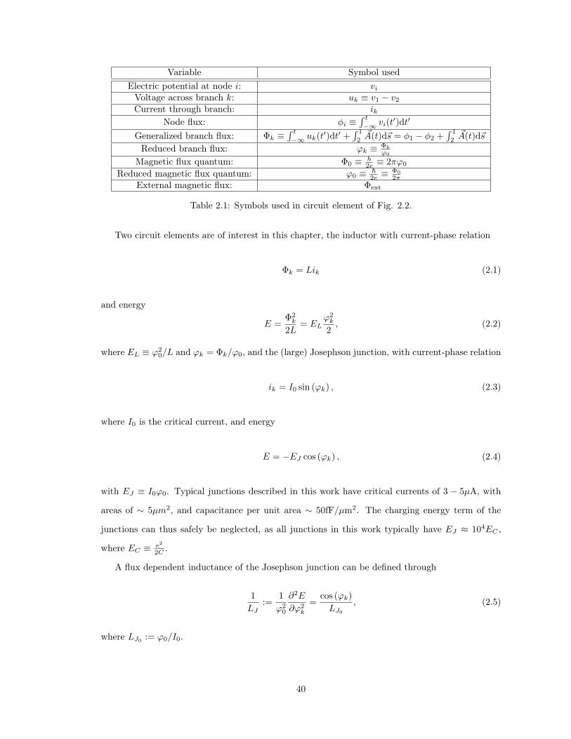
Variable Symbol usedElectric potential at node i: viVoltage across branch k: uk ≡ v1 − v2
Current through branch: ikNode flux: φi ≡
´ t−∞ vi(t
′)dt′
Generalized branch flux: Φk ≡´ t−∞ uk(t′)dt′ +
´ 1
2~A(t)d~s = φ1 − φ2 +
´ 1
2~A(t)d~s
Reduced branch flux: ϕk ≡ Φkϕ0
Magnetic flux quantum: Φ0 ≡ h2e ≡ 2πϕ0
Reduced magnetic flux quantum: ϕ0 ≡ ~2e ≡
Φ0
2π
External magnetic flux: Φext
Table 2.1: Symbols used in circuit element of Fig. 2.2.
Two circuit elements are of interest in this chapter, the inductor with current-phase relation
Φk = Lik (2.1)
and energy
E =Φ2k
2L= EL
ϕ2k
2, (2.2)
where EL ≡ ϕ20/L and ϕk = Φk/ϕ0, and the (large) Josephson junction, with current-phase relation
ik = I0 sin (ϕk) , (2.3)
where I0 is the critical current, and energy
E = −EJ cos (ϕk) , (2.4)
with EJ ≡ I0ϕ0. Typical junctions described in this work have critical currents of 3 − 5µA, with
areas of ∼ 5µm2, and capacitance per unit area ∼ 50fF/µm2. The charging energy term of the
junctions can thus safely be neglected, as all junctions in this work typically have EJ ≈ 104EC ,
where EC ≡ e2
2C .
A flux dependent inductance of the Josephson junction can be defined through
1
LJ:=
1
ϕ20
∂2E
∂ϕ2k
=cos (ϕk)
LJ0
, (2.5)
where LJ0 := ϕ0/I0.
40
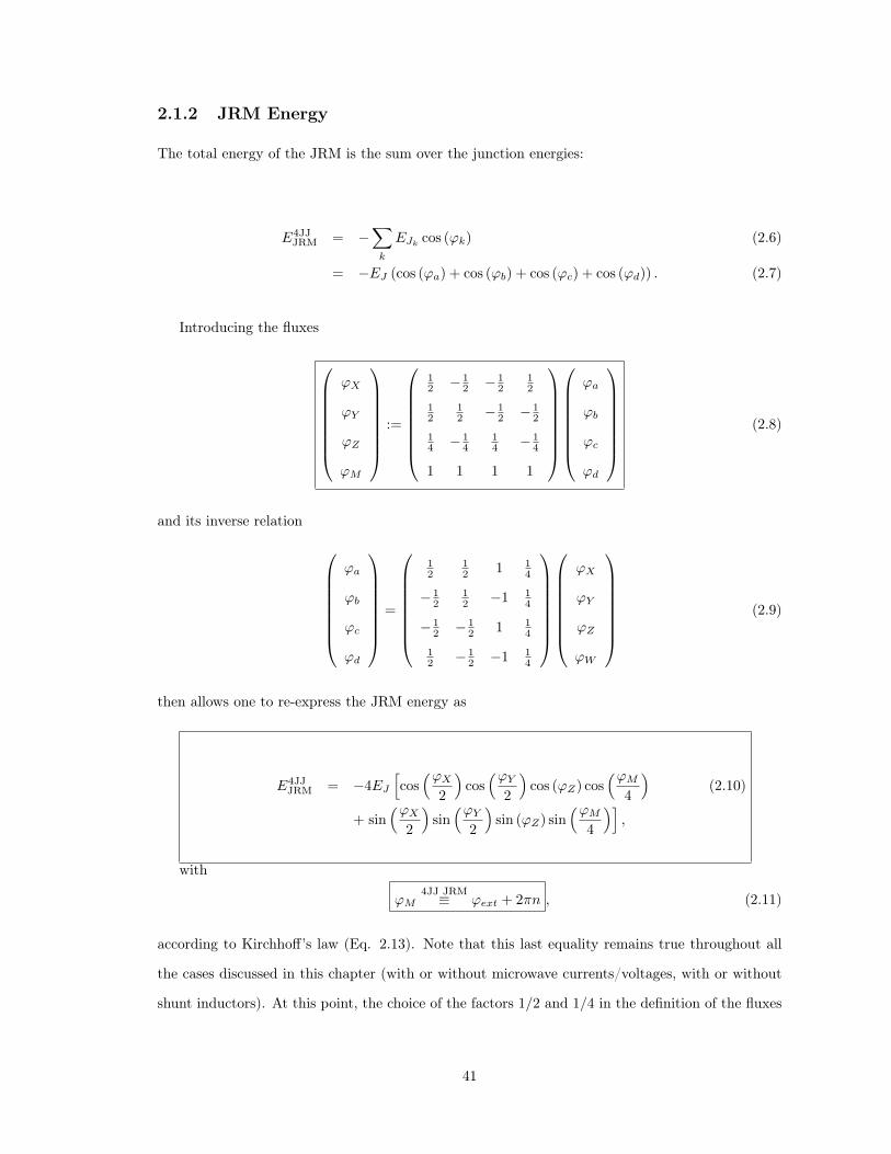
2.1.2 JRM Energy
The total energy of the JRM is the sum over the junction energies:
E4JJJRM = −
∑k
EJk cos (ϕk) (2.6)
= −EJ (cos (ϕa) + cos (ϕb) + cos (ϕc) + cos (ϕd)) . (2.7)
Introducing the fluxes
ϕX
ϕY
ϕZ
ϕM
:=
12 − 1
2 − 12
12
12
12 − 1
2 − 12
14 − 1
414 − 1
4
1 1 1 1
ϕa
ϕb
ϕc
ϕd
(2.8)
and its inverse relation
ϕa
ϕb
ϕc
ϕd
=
12
12 1 1
4
− 12
12 −1 1
4
− 12 − 1
2 1 14
12 − 1
2 −1 14
ϕX
ϕY
ϕZ
ϕW
(2.9)
then allows one to re-express the JRM energy as
E4JJJRM = −4EJ
[cos(ϕX
2
)cos(ϕY
2
)cos (ϕZ) cos
(ϕM4
)(2.10)
+ sin(ϕX
2
)sin(ϕY
2
)sin (ϕZ) sin
(ϕM4
)],
with
ϕM4JJ JRM≡ ϕext + 2πn , (2.11)
according to Kirchhoff’s law (Eq. 2.13). Note that this last equality remains true throughout all
the cases discussed in this chapter (with or without microwave currents/voltages, with or without
shunt inductors). At this point, the choice of the factors 1/2 and 1/4 in the definition of the fluxes
41

ϕX,Y,Z is not obvious. It will become clear shortly (Eq. 2.24 ff.) that these factors make it possible
to identify ϕX,Y,Z to be exactly the relevant generalized branch fluxes of the system.
There are four distinct energy states, parametrized by n = 0, 1, 2, 3. For small fluxes, ϕX,Y,Z
1, the energy term becomes
E4JJJRM
ϕX,Y,Z1= −EJ sin
(ϕext4
+ nπ
2
)ϕXϕY ϕZ + EJ cos
(ϕext4
+ nπ
2
)(ϕ2X
2+ϕ2Y
2+ 2ϕ2
Z − 4
)(2.12)
and thus has the desired mixing form ∼ ϕXϕY ϕZ . The terms in ϕ2X,Y,Z merely renormalized the
mode frequencies and don’t lead to any unwanted additional nonlinear mixing. The ϕXϕY ϕZ form
in itself is not sufficient, as the fluxes ϕX,Y,Z defined above have to have the “correct” dependence
of externally applied microwave voltages at the nodes in order to be meaningful variables. As will
be shown below, this is the case and the ϕX,Y,Z can be expressed as differences of the node fluxes
φi, which justifies the choice of the modes X,Y, Z through Eq. 2.8. Note also that Eq. 2.12 has a
coupling energy term −EJ sin(ϕext
4 + nπ2)whose sign depends on the external magnetic flux. This
leads to a phase difference of π in the mixing term g3 and thus ultimately to a π phase shift in the
two-mode squeezing parameter phase ϕ (see Eq. 3.42).
2.1.3 Current Induced by Magnetic Flux
Before treating the general case of externally applied direct current (DC) magnetic field and radio
frequency (RF) microwave currents and voltages, consider the case where just a (DC) external
magnetic flux Φext is applied, but without any applied microwave fields. Let Φk, k ∈ a, b, c, d be
the generalized flux across junction k (at branch k) as seen in the schematic of Fig. 2.1.
Applying Kirchhoff’s laws for currents and fluxes together with flux quantization yields
Φa + Φb + Φc + Φd = Φext + nΦ0 (2.13)
−ia + id = 0 (2.14)
−ic + ib = 0 (2.15)
−id + ic = 0 (2.16)
−ib + ia = 0, (2.17)
42

where n ∈ Z. Together with the Josephson relation ik = I0 sin (Φk/ϕ0) this leads to the solution
ΦDCa = ΦDC
b = ΦDCc = ΦDC
d4JJ-JRM
=Φext
4+ n
Φ0
4(2.18)
and
iDCa = iDC
b = iDCc = iDC
d4JJ-JRM
= I0 sin(ϕext
4+ n
π
2
), (2.19)
where the notation ΦDCk and iDC
k is used to indicate that these solutions correspond to currents and
fluxes which are due only to the external applied magnetic field. Equation 2.19 shows that a DC
magnetic flux threading the loop will lead to four different possible circulating current configurations
in the ring: ±I0 sin (ϕext/4) and ±I0 cos (ϕext/4) .
2.1.4 Adding External Microwaves
When connecting nodes 1, 2, 3, 4 to an outside circuit, the influence of possible additional microwave
currents/voltages on the fluxes Φa,b,c,d and thus ΦX,Y,Z,M has to be considered. As mentioned
above, ΦM ≡ Φext + nΦ0, so it is decoupled from outside currents/voltages. These RF voltages
will influence the node fluxes, while the vector potential ~A (i.e. the applied magnetic field) remains
unaffected. In general one can write
φi = φDCi + φRFi , (2.20)
where φDCi is the node flux due to the magnetic field, and φRFi the node flux due to the microwave
field. It then follows that Φk = ΦDCk + ΦRF
k and since Eqs. 2.8 are linear, also that
ΦX = φRF3 − φRF4 + ΦDCX (2.21)
ΦY = φRF1 − φRF2 + ΦDCY (2.22)
ΦZ =φRF1 + φRF2 − φRF3 − φRF4
2+ ΦDC
Z . (2.23)
Since ΦDCX,Y,Z
4JJ-JRM= 0 in the four junction JRM (Eqs. 2.8 and 2.18), one finally arrives at
43

ΦX4JJ-JRM
= φRF3 − φRF4 (2.24)
ΦY4JJ-JRM
= φRF1 − φRF2 (2.25)
ΦZ4JJ-JRM
=φRF1 + φRF2 − φRF3 − φRF4
2. (2.26)
These expressions justify the choice of ΦX,Y,Z as relevant generalized branch fluxes. For instance,
when the JRM is inserted into a circuit as a two-node (black-box) element with nodes 3 and 4, then
ΦX is simply the generalized branch flux across this element.
2.1.5 Lowest Ring Energy
When no microwave currents/voltages are applied, ϕX,Y,Z = 0 and the energy expression reduces
to
E4JJJRM
ϕX,Y,Z=0= −4EJ cos
(ϕext4
+ nπ
2
), (2.27)
with n = 0, 1, 2, 3. Figure 2.3 shows the four magnetic flux degenerate energy states together with
the lowest energy envelopes. Since there is a potential barrier to switching from energy state n to
n′ 6= n, there will be hysteresis, i.e. the energy state depends on the sweep direction, as indicated
in Fig. 2.3 b).
2.1.6 Current-Flux Relation
The current-flux relation for modes X,Y, Z can be found by noting that the JRM is a non-linear
inductance, with
L−1X,Y,Z :=
1
ϕ20
∂2E
∂ϕ2X,Y,Z
. (2.28)
So in the case where Φk 6= 0, while Φk′ = 0 for k, k′ ∈ X,Y, Z, and using Eq. 2.10, one finds
L−1X
ϕY,Z=0= L−1
J cos(ϕX
2
)cos(ϕext
4+ n
π
2
)(2.29)
L−1Y
ϕX,Z=0= L−1
J cos(ϕY
2
)cos(ϕext
4+ n
π
2
)(2.30)
L−1Z
ϕX,Y =0= 4L−1
J cos(ϕZ
2
)cos(ϕext
4+ n
π
2
), (2.31)
44

-1.0
-0.5
0.0
0.5
1.0E
/(4E
J)E
/(4E
J)
-1.0
-0.5
0.0
0.5
1.0
0 1 2 3 4Φext/Φ0
a)
b)
n=0
n=1
n=2
n=3
Figure 2.3: JRM energy for ϕX,Y,Z = 0. a) Schematic of magnetic flux degenerate energy states(colored) and lowest energy envelope (black). b) Same as a), but with hysteresis. Dependingon the magnetic field sweep direction, different energy states are attained (black and gray). Anenergy barrier (not shown here) separates the different flux states and is associated with the costof entrance of additional flux quanta into the loop [68]. The exact locations of jumps between fluxstates are determined by the barrier height and the amount of noise present in the system. JPCworking points are typically at Φ0/2 (mod Φ0), indicated by the white disk.
45
where LJ ≡ I0/ϕ0. Again, four different solutions are found, parametrized by n = 0, 1, 2, 3. The
JRM thus has a current-flux relation very similar to a single junction, with a critical current reduced
by the external field. To first order in ϕX,Y,Z 1, one finds
4JJ JRM: L−1X,Y
ϕX,Y,Z0= L−1
J cos(ϕext
4+ n
π
2
)(2.32)
L−1Z
ϕX,Y,Z0= 4L−1
J cos(ϕext
4+ n
π
2
). (2.33)
2.1.7 Experiment
The JRM energy state as a function of Φext can be monitored in the JPC by measuring the
resonance frequency of e.g. the signal mode as a function of the applied magnetic flux. When
no idler and pump tones are applied, no coupling between modes ϕX,Y,Z exists, as ϕY,Z = 0 and
the ring modulator energy (Eq. 2.10) reduces to E4JJJRM
ϕY,Z=0= −4EJ cos
(ϕX2
)cos(ϕext
4 + nπ2). For
small signal probe powers (ϕX 1), the inductance of the JRM is given by Eq. 2.32, and the
equivalent circuits are shown in Fig. 2.4. a) Shows the equivalent JPC circuit for balanced coupling
through a 180-degree hybrid coupler, while b) shows the JPC circuit when one of the transmission
line resonator ports is shorted to ground. Some of the devices fabricated were of the type shown in
a) on the idler port, while being of type shown in b) on the signal port. In either case, around their
respective resonance frequencies they can be represented by LC-circuits with a linear inductor in
series with the nonlinear inductance given by the JRM (Eq. 2.32).
Figure 2.5 shows a picture of a typical JRM fabricated using the Dolan bridge technique [62].
The junctions are in the range of I0 = 3− 5µA and have an area of 5× 1µm2.
2.1.7.1 Flux Modulation
When varying the magnetic flux through the JRM and measuring the phase response of the JPC
signal or idler ports (without pump tone), the degeneracy of the energy state can be observed, as
the system is hysteretic.
As seen in Fig. 2.6 a) and b), the resonance frequencies are changing with the magnetic field
and jumps occur, which correspond to a change in energy states (n = 0 → n = 3 → n = 2 →
n = 1 → n = 0 when increasing the flux). When reversing the sweep direction of the flux, the
jump locations change and hysteresis can be observed. The yellow traces are the resonator center
46

a)
b)
Φext
50Ω∆ Σ
Φext
Figure 2.4: Schematic of transmission line resonators with 4JJ JRM. a) Symmetric coupling through180-degree hybrid. b) Single ended resonator. This type of transmission line resonator has theadvantage that no hybrid coupler is needed to excite its differential mode, but the disadvantagethat the current anti-node is shifted from its geometric mid-point, where the JRM is usually located.
5μm
Figure 2.5: A four junction JRM fabricated with e-beam lithography and using the Dolan bridgetechnique.
47

5.5
5.4
5.3
5.2
5.1
Freq
uenc
y (G
Hz)
-1/2 0 1/2 1 3/2 2 5/2 3 7/2Flux Quanta
7.4
7.2
7.0
6.8
Freq
uenc
y (G
Hz)
-1/2 0 1/2 1 3/2 2 5/2 3 7/2Flux Quanta
-180-120-60060120180
Phase (deg.)
a)
b)
Figure 2.6: Phase response of JPC for modulated magnetic flux. No pump power is applied. a)Reflected phase of microwaves injected on signal port. 2D color plot: phase for increasing magneticflux. Yellow trace: resonance frequency for increasing magnetic flux. White trace: resonancefrequency for decreasing magnetic flux. b) Same as a), but for idler resonator. The signal resonatorof this sample (JPX30; JRM similar to one shown in Fig. 2.5) is of the type shown in Fig. 2.4 b),while the idler resonator is of the type shown in Fig. 2.4 a).
48
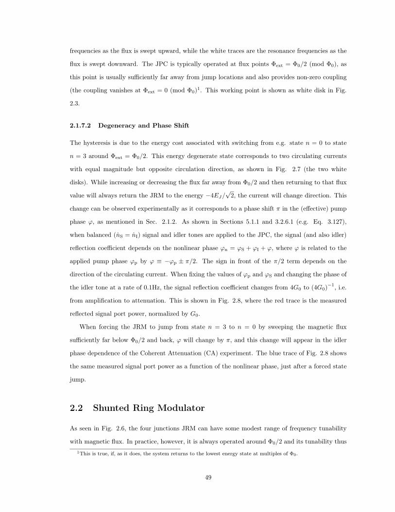
frequencies as the flux is swept upward, while the white traces are the resonance frequencies as the
flux is swept downward. The JPC is typically operated at flux points Φext = Φ0/2 (mod Φ0), as
this point is usually sufficiently far away from jump locations and also provides non-zero coupling
(the coupling vanishes at Φext = 0 (mod Φ0)1. This working point is shown as white disk in Fig.
2.3.
2.1.7.2 Degeneracy and Phase Shift
The hysteresis is due to the energy cost associated with switching from e.g. state n = 0 to state
n = 3 around Φext = Φ0/2. This energy degenerate state corresponds to two circulating currents
with equal magnitude but opposite circulation direction, as shown in Fig. 2.7 (the two white
disks). While increasing or decreasing the flux far away from Φ0/2 and then returning to that flux
value will always return the JRM to the energy −4EJ/√
2, the current will change direction. This
change can be observed experimentally as it corresponds to a phase shift π in the (effective) pump
phase ϕ, as mentioned in Sec. 2.1.2. As shown in Sections 5.1.1 and 3.2.6.1 (e.g. Eq. 3.127),
when balanced (nS = nI) signal and idler tones are applied to the JPC, the signal (and also idler)
reflection coefficient depends on the nonlinear phase ϕn = ϕS + ϕI + ϕ, where ϕ is related to the
applied pump phase ϕp by ϕ ≡ −ϕp ± π/2. The sign in front of the π/2 term depends on the
direction of the circulating current. When fixing the values of ϕp and ϕS and changing the phase of
the idler tone at a rate of 0.1Hz, the signal reflection coefficient changes from 4G0 to (4G0)−1, i.e.
from amplification to attenuation. This is shown in Fig. 2.8, where the red trace is the measured
reflected signal port power, normalized by G0.
When forcing the JRM to jump from state n = 3 to n = 0 by sweeping the magnetic flux
sufficiently far below Φ0/2 and back, ϕ will change by π, and this change will appear in the idler
phase dependence of the Coherent Attenuation (CA) experiment. The blue trace of Fig. 2.8 shows
the same measured signal port power as a function of the nonlinear phase, just after a forced state
jump.
2.2 Shunted Ring Modulator
As seen in Fig. 2.6, the four junctions JRM can have some modest range of frequency tunability
with magnetic flux. In practice, however, it is always operated around Φ0/2 and its tunability thus1This is true, if, as it does, the system returns to the lowest energy state at multiples of Φ0.
49

-1.0
-0.5
0.0
0.5
1.0
I/I0 n=1 n=0 n=3 n=2
0 1 2 3 4Φext/Φ0
Figure 2.7: Circulating current in JRM induced by magnetic flux. Working points are typicallyat Φ0/2 (mod Φ0) and indicated by the two white disks, representing clockwise and anti-clockwisecirculating currents. These two states are degenerate in energy (see Fig. 2.3). Note that the currentdirection is defined in Fig. 2.2, so that a positive current is flowing in the opposite direction of theintegration path defining Φext.
-50
-40
-30
-20
-10
06
Pow
er (d
B)
13/41/21/40 (rad/2φ/2π = δf∙t π)
Figure 2.8: Coherent attenuation experiment at degenerate flux point Φext = Φ0/2 (sample JPX26).The reflected signal port power is measured as a function of the idler phase, which is changed at arate of 0.1Hz. Red trace: flux is set to Φ0/2 (in decreasing field sweep direction). Blue trace: fluxalso set to Φ0/2, but only after sweeping it below Φext = 0 and back up, to induce jump in JRMstate.
50

a d
cb
1
2
34
a d
cb
1
2
34
Φaia
id
ic
ib
iL2
iL4 iL1
iL3
Φd
Φb
Φc
ΦL1ΦL4
ΦL3
ΦL2
Figure 2.9: Schematic of shunted Josephson ring modulator. The sign of currents is defined withrespect to the red arrows, while the sign of fluxes is defined with respect to the green arrows.
very limited. At fluxes Φext between 0 and Φ0/2, there is not much change in the JPC frequency, as
LX (defined in Eq. 2.32) changes only by ∼ 30%, and makes up only ∼ 5% of the total equivalent
resonator inductance. Further, and more importantly, the coupling term between modes X,Y, Z
goes as sin (ϕext/4) (Eq. 2.12), so that it vanishes around Φext = 0. Beyond Φext = Φ0/2 however,
the device becomes more sensitive to magnetic field noise and more likely to undergo flux state
jumps.
The degeneracy can be lifted by quartering the ring with shunt inductors, which will create
four loops with only one junction per loop, as seen in Fig. 2.9. As will be shown below, when
using Kirchhoff’s loop rule and evaluating the integralı~Ad~s = Φloop+nloopΦ0, the term nloopΦ0 is
entirely absorbed by the junction flux, which is unique up to multiples of Φ0 anyways, so that the
degeneracy is lifted. Note that simply shunting each junction outside of the loop will not lift the
degeneracy, but will simply create an uncoupled current through the inductors, while the junction
current is still set by the flux through the large loop2.2One could think of it as two independent rings: an unshunted JRM and a ring with four linear inductors.
51

a d
cb
1
2
34na nd
nb nc
a d
cb
1
2
34 Φext
Figure 2.10: Schematic of JRM with magnetic flux quanta in each loop (left) and external magneticflux (right). The flux Φext is defined with respect to the area enclosed by the four outer junctions.
2.2.1 Circuit Equations
It is useful to write out the circuit equations for the JRM in the absence of external (microwave)
currents and voltages, in order to understand how the energy states are parametrized. The loop
rule gives (with or without external currents/voltages)
Φa − ΦL1+ ΦL4
=Φext
4+ naΦ0 (2.34)
Φb − ΦL4 + ΦL2 =Φext
4+ nbΦ0 (2.35)
Φc − ΦL2+ ΦL3
=Φext
4+ ncΦ0 (2.36)
Φd − ΦL3 + ΦL1 =Φext
4+ ndΦ0, (2.37)
where Φext is the external magnetic flux threading the area enclosed by the four junctions, and the
na,b,c,d ∈ Z are the flux quanta per partial loop, as shown in Fig. 2.10. The Φk, k ∈ a, b, c, d and
ΦLi , i ∈ 1, 2, 3, 4 are the generalized fluxes shown in Fig. 2.9.
52

The node rule (without external currents) gives
id − ia − iL1= 0 (2.38)
ib − ic − iL2= 0 (2.39)
ic − id − iL3= 0 (2.40)
ia − ib − iL4 = 0, (2.41)
where the i are the currents again shown in Fig. 2.9. With identical junctions and inductors, the
current-flux relations are
ik = I0 sin (ϕk) k ∈ a, b, c, d (2.42)
iLi =1
LΦLi i ∈ 1, 2, 3, 4 , (2.43)
where ϕk ≡ Φk/ϕ0.
2.2.2 Shunted JRM Energy
The goal is again to show that the energy term of the shunted JRM provides a mixing of the modes
of the form ϕXϕY ϕZ , for certain values of the external magnetic flux Φext. The energy of the
shunted ring modulator is given by
EshuntedJRM = −EJ [cos (ϕa) + cos (ϕb) + cos (ϕc) + cos (ϕd)] (2.44)
+EL2
[ϕ2L1
+ ϕ2L2
+ ϕ2L3
+ ϕ2L4
],
where EL ≡ ϕ20/L, EJ ≡ ϕ2
0/LJ0, and LJ0
≡ ϕ0/I0. The modes X,Y, Z are again defined in Eq.
2.8, and again, the M mode is decoupled from the JRM, since
ϕMshunted JRM≡ ϕext + 2π
∑k
nk . (2.45)
The difference to the four junction case (Eq. 2.11) is that (∑k nk/4) ∈ Z, so that the Josephson
term can be expressed as
53

E = −EJ [cos (ϕa) + cos (ϕb) + cos (ϕc) + cos (ϕd)] (2.46)
= −4EJ
[cos(ϕX
2
)cos(ϕY
2
)cos (ϕZ) cos
(ϕext4
)(2.47)
+ sin(ϕX
2
)sin(ϕY
2
)sin (ϕZ) sin
(ϕext4
)].
The degeneracy of this term is now lifted (compare to Eq. 2.10), as the magnetic field enters with
unique values as cos (ϕext /4) and sin (ϕext /4).
For any value of (na, nb, nc, nd), the inductive part can be expressed as
ϕ2L1
+ ϕ2L2
+ ϕ2L3
+ ϕ2L4
=ϕ2X
2+ϕ2Y
2+ ϕ2
Z (2.48)
+2π2(n2X + n2
Y + 2n2Z
)−2π (nXϕX + nY ϕY + 2nZϕZ)
=(ϕX − 2πnX)
2
2+
(ϕY − 2πnY )2
2(2.49)
+ (ϕZ − 2πnZ)2,
where the nX,Y,Z are defined analogous to the ϕX,Y,Z :
nX :=na − nb − nc + nd
2(2.50)
nY :=na + nb − nc − nd
2(2.51)
nZ :=na − nb + nc − nd
4. (2.52)
Note that in general the nX,Y,Z need not be integers, but rather multiples of ±1/2 or ±1/4.
So finally the shunted JRM energy can be expressed as:
54

EshuntedJRM = −4EJ
[cos(ϕX
2
)cos(ϕY
2
)cos (ϕZ) cos
(ϕext4
)(2.53)
+ sin(ϕX
2
)sin(ϕY
2
)sin (ϕZ) sin
(ϕext4
)]+EL2
[(ϕX − 2πnX)
2
2+
(ϕY − 2πnY )2
2+ (ϕZ − 2πnZ)
2
].
Just as in the case of the unshunted JRM, this energy has the useful ϕXϕY ϕZ nonlinear mixing
term for small ϕX,Y,Z , but it still needs to be assured that the modes X,Y, Z are the relevant ones.
Again, in general the branch fluxes can be expressed as superpositions between DC fluxes ΦDC
induced by the applied external magnetic field Φext and the RF fluxes ΦRF due to the externally
applied microwave fields, Φk = ΦDCk +ΦRF
k . By noting that the vector potential terms´~Ad~s remain
the same with or without the ΦRF terms, it is not difficult to show that for any state (na, nb, nc, nd)
the ΦX,Y,Z can be expressed as functions of the (applied) node fluxes φRFi , i ∈ 1, 2, 3, 4:
ΦX = φRF3 − φRF4 + ΦDCX (2.54)
ΦY = φRF1 − φRF2 + ΦDCY (2.55)
ΦZ =φRF1 + φRF2 − φRF3 − φRF4
2+ ΦDC
Z . (2.56)
To determine the energy mixing term, all that remains to do is to find the magnetic field induced
fluxes ΦDCX,Y,Z , or equivalently, the circulating DC currents in the ring.
The JRM energy state can be parametrized by the integers (na, nb, nc, nd) and two cases
with high symmetry are of interest and considered below: (na, nb, nc, nd) = (m,m,m,m) and
(na, nb, nc, nd) = (m,−m,m,−m), where m ∈ Z.
2.2.3 Solutions (m,m,m,m)
In this case,∑k nk = 4m and nX,Y,Z = 0, ∀m ∈ Z.
2.2.3.1 Circulating Currents
Solving Kirchhoff’s Eqs. 2.34ff. and 2.38ff. one finds
55

ϕext < 0 ϕext = 0 ϕext > 0
Figure 2.11: Current pattern for the state (m,m,m,m) around ϕext = 0. The arrows indicate thedirection of the current flow, while the dots indicate that the circulating currents are zero.
ΦDCa,b,c,d
(m,m,m,m)=
Φext
4+mΦ0 (2.57)
⇒ iDCa,b,c,d
(m,m,m,m)= I0 sin
(ϕext4
)(2.58)
ΦDCL1,2,3,4
(m,m,m,m)= 0 (2.59)
⇒ iDCL1,2,3,4
(m,m,m,m)= 0. (2.60)
Figure 2.11 shows the current pattern for this state, centered around ϕext = 0. No current
flows through the central inductors, while a current is circulating in the loop defined by the four
junctions, and whose direction and magnitude is uniquely determined by the magnetic flux ϕext.
In particular, this means that
ΦDCX,Y,Z
(m,m,m,m)= 0 (2.61)
and thus that
ΦX(m,m,m,m)
= φRF3 − φRF4 =: ΦRFX (2.62)
ΦY(m,m,m,m)
= φRF1 − φRF2 =: ΦRFY (2.63)
ΦZ(m,m,m,m)
=φRF1 + φRF2 − φRF3 − φRF4
2=: ΦRF
Z , (2.64)
which is the desired dependence on the φRF.
56

2.2.3.2 Energy
Thus Eq. 2.53 becomes
EshuntedJRM
(m,m,m,m)= −4EJ
[cos
(ϕRFX
2
)cos
(ϕRFY
2
)cos(ϕRFZ
)cos(ϕext
4
)(2.65)
+ sin
(ϕRFX
2
)sin
(ϕRFY
2
)sin(ϕRFZ
)sin(ϕext
4
)]+EL2
[(ϕRFX
)22
+
(ϕRFY
)22
+(ϕRFZ
)2].
The energy expression shows in particular that no dependence on the parameter m ∈ Z exists,
which means that all solutions (m,m,m,m) are in fact physically identical.
For small ϕRFX,Y,Z , one obtains the desired mixing term ϕRFX ϕRFY ϕRFZ , but this time without
degeneracy:
EshuntedJRM (m,m,m,m)
ϕRFX,Y,Z1
= −EJ sin(ϕext
4
)ϕRFX ϕRFY ϕRFZ (2.66)
+
(EJ cos
(ϕext4
)+EL2
)((ϕRFX
)22
+
(ϕRFY
)22
)
+2
(EJ cos
(ϕext4
)+EL4
)(ϕRFZ
)2−4EJ cos
(ϕext4
).
It is this energy state that is of interest for the parametric amplification process, and care has
to be taken to ensure the JRM is operated in this state. Below it will be shown for which magnetic
fluxes this state is attained. For ϕRFX,Y,Z = 0, the energy reduces to the non-degenerate value
EshuntedJRM (m,m,m,m)
ϕRFX,Y,Z=0
= −4EJ cos(ϕext
4
). (2.67)
2.2.3.3 Equivalent Inductance
Using Eq. 2.283 for ϕRFX,Y,Z 1 the magnetic field dependent equivalent inductances of the shunted
JRM become3The derivative is of course with respect to ϕRFX,Y,Z .
57

shunted JRM:
(m,m,m,m) L−1X,Y
ϕRFX,Y,Z1
=L−1
2
(2βL cos
(ϕext4
)+ 1)
(2.68)
L−1Z
ϕRFX,Y,Z1
= L−1(
4βL cos(ϕext
4
)+ 1), (2.69)
where βL ≡ L/LJ0= EJ/EL. Note that Eq. 2.68 is the solution also found through simple cir-
cuit analysis, by assuming that the junctions are linear inductors with inductance LJ/ cos(ϕext/4).
2.2.4 Solutions (m,−m,m,−m)
The second set of solutions of interest are those for which (na, nb, nc, nd) = (m,−m,m,−m), m ∈ Z,
or equivalently (nX , nY , nZ , nW ) = (0, 0,m, 0), where nW :=∑k∈a,b,c,d nk.
2.2.4.1 Circulating Currents
Solving the loop and node equations, one finds
ΦDCa,c
(m,−m,m,−m)= + (xϕ0 +mΦ0) +
Φext
4(2.70)
ΦDCb,d
(m,−m,m,−m)= − (xϕ0 +mΦ0) +
Φext
4(2.71)
⇒ iDCa,c
(m,−m,m,−m)= I0 sin
(x+
ϕext4
)(2.72)
⇒ iDCb,d
(m,−m,m,−m)= I0 sin
(−x+
ϕext4
)(2.73)
ΦDCL1,2
(m,−m,m,−m)= −ΦDC
L3,4=x
2ϕ0 (2.74)
⇒ iDCL1,2
(m,−m,m,−m)= −iDC
L3,4=xϕ0
2L, (2.75)
where x is solution to the RF-superconducting quantum interference device (SQUID)-like equation
x = −4βL cos(ϕext
4
)sin (x) , (2.76)
with βL := LLJ0≡ EJ
EL.
Figure 2.12 shows the current pattern found above, centered around ϕext = 4π. This time, a
current flows through the central inductors, given by xϕ0/(2L). At magnetic fluxes away from 4π,
the current through the shunt inductors remains the same, but the junction currents are pairwise
58
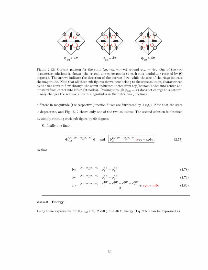
ϕext < 4π ϕext = 4π ϕext > 4π
Figure 2.12: Current pattern for the state (m,−m,m,−m) around ϕext = 4π. One of the twodegenerate solutions is shown (the second one corresponds to each ring modulator rotated by 90degrees). The arrows indicate the direction of the current flow, while the size of the rings indicatethe magnitude. Note that all three sub-figures shown here belong to the same solution, characterizedby the net current flow through the shunt inductors (here: from top/bottom nodes into center andoutward from center into left/right nodes). Passing through ϕext = 4π does not change this pattern,it only changes the relative current magnitudes in the outer ring junctions.
different in magnitude (the respective junction fluxes are frustrated by ±xϕ0). Note that the state
is degenerate, and Fig. 2.12 shows only one of the two solutions. The second solution is obtained
by simply rotating each sub-figure by 90 degrees.
So finally one finds
ΦDCX,Y
(m,−m,m,−m)= 0 and ΦDC
Z
(m,−m,m,−m)= xϕ0 +mΦ0 , (2.77)
so that
ΦX(m,−m,m,−m)
= φRF3 − φRF4 (2.78)
ΦY(m,−m,m,−m)
= φRF1 − φRF2 (2.79)
ΦZ(m,−m,m,−m)
=φRF1 + φRF2 − φRF3 − φRF4
2+ xϕ0 +mΦ0. (2.80)
2.2.4.2 Energy
Using these expressions for ΦX,Y,Z (Eq. 2.78ff.), the JRM energy (Eq. 2.53) can be expressed as
59
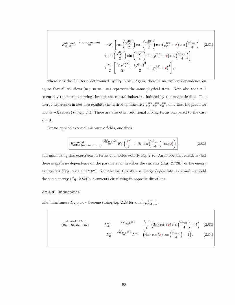
EshuntedJRM
(m,−m,m,−m)= −4EJ
[cos
(ϕRFX
2
)cos
(ϕRFY
2
)cos(ϕRFZ + x
)cos(ϕext
4
)(2.81)
+ sin
(ϕRFX
2
)sin
(ϕRFY
2
)sin(ϕRFZ + x
)sin(ϕext
4
)]+EL2
[(ϕRFX
)22
+
(ϕRFY
)22
+(ϕRFZ + x
)2],
where x is the DC term determined by Eq. 2.76. Again, there is no explicit dependence on
m, so that all solutions (m,−m,m,−m) represent the same physical state. Note also that x is
essentially the current flowing through the central inductors, induced by the magnetic flux. This
energy expression in fact also exhibits the desired nonlinearity ϕRFX ϕRFY ϕRFZ , only that the prefactor
now is −EJ cos(x) sin(ϕext/4). There are also other additional mixing terms compared to the case
x = 0.
For no applied external microwave fields, one finds
EshuntedJRM (m,−m,m,−m)
ϕRFX,Y,Z=0
= EL
(x2
2− 4βL cos
(ϕext4
)cos (x)
), (2.82)
and minimizing this expression in terms of x yields exactly Eq. 2.76. An important remark is that
there is again no dependence on the parameter m in either the currents (Eqs. 2.72ff.) or the energy
expressions (Eqs. 2.81 and 2.82). Nonetheless, this state is energy degenerate, as x and −x yield
the same energy (Eq. 2.82) but currents circulating in opposite directions.
2.2.4.3 Inductance
The inductances LX,Y now become (using Eq. 2.28 for small ϕRFX,Y,Z):
shunted JRM:
(m,−m,m,−m) L−1X,Y
ϕRFX,Y,Z1
=L−1
2
(2βL cos (x) cos
(ϕext4
)+ 1)
(2.83)
L−1Z
ϕRFX,Y,Z1
= L−1(
4βL cos (x) cos(ϕext
4
)+ 1). (2.84)
60

30
20
10
0
-10
EJR
M
/EL
-2π -3/2π -π -1/2π 0 1/2π π 3/2π 2πx
−4βLcos(ϕext/4) = 1 −4βLcos(ϕext/4) > 1 −4βLcos(ϕext/4) = 1/cos(x0) ≈ −4.55 −4βLcos(ϕext/4) < 1/cos(x0)
(m,-m
,m,-m
)
Figure 2.13: JRM energy as a function of x, for different values of −4βL cos(ϕext/4). The dotscorrespond to local and global energy minima. The blue trace corresponds to the case where∃x 6= 0 which are the energetically most favorable solutions and the ring modulator is in state(m,−m,m,−m). All other cases lead to x = 0 and the ring modulator is in state (m,m,m,m).
2.2.5 Crossover
As stated above, it is desirable to operate the JRM in the regime corresponding to state (m,m,m,m),
so it is important to understand which energy expression (Eq. 2.65 or Eq. 2.81) describes the JRM
for a given magnetic flux. This comes down to comparing the energy expressions in the two cases
for ϕRFX,Y,Z = 0, i.e. Eq. 2.67 and 2.82. It is clear that for x = 0, the two states are identical, so
that one needs to find the condition for when x 6= 0, and one needs to distinguish between different
cases.
ϕext ∈ [0, 2π] ∪ [6π, 8π]: amplification always possible
This is the flux region where cos(ϕext4 ) > 0 and which is of interest for parametric amplification,
as the state (m,m,m,m) is always minimizing the energy. There are solutions x 6= 0 as long as
the magnetic flux and βL satisfy −4βL cos(x0) cos(ϕext/4) > 1, where x0 ≈ 4.495 and − cos(x0) ≈
+0.22 are given by the tangent equation x0!= tan(x0). However, these solutions represent local
minima, while x = 0 remains the global energy minimum solution. The other case, where 0 <
−4βL cos(x0) cos(ϕext/4) < 1, has x = 0 as only solution. Thus in this magnetic flux region, the
JRM is always described by the state labeled (m,m,m,m) above, and Eq. 2.65 holds. The red and
pink trace in Fig. 2.13 show the JRM energy as a function of x for −4βL cos(x0) cos(ϕext/4) = 1
and −4βL cos(x0) cos(ϕext/4) > 1, respectively.
61

ϕext ∈ [2π, 6π]: amplification sometimes possible
In this region, cos(ϕext4 ) < 0 and the state (m,m,m,m) minimizes the energy only for particular
flux values. Solutions x = ±x1 6=0 exist for −4βL cos(ϕext/4) > 1 and these solutions correspond to
global minima, leading to the state (m,−m,m,−m). The black and blue traces in Fig. 2.13 show
the energy for −4βL cos(ϕext/4) = 1 and −4βL cos(ϕext/4) > 1, respectively. For a given shunted
JRM described by βL ≡ L/LJ0, the magnetic flux ϕcrossoverext ∈ ]2π, 4π[ at which the crossover
between the state (m,m,m,m) and the state (m,−m,m−m) occurs, is given by
−4βL cos(ϕcrossoverext /4) = 1 . (2.85)
This equation does not necessarily have solutions. In the case that the shunt inductors are suf-
ficiently small so that 4L < LJ (4βL < 1), the mode (m,m,m,m) is stable, and parametric
amplification still possible. This happens at the expense of frequency tunability, as LX,Y remains
small for any magnetic field Φext (see Eq. 2.68). Additionally, by lowering L, EL becomes large
and starts to significantly alter the JPC resonance frequency.
Equation 2.68 suggests that the inductance LX,Y can become negative and thus ill-defined
for fluxes such that −2βL cos(ϕext/4) > 1, that is, only if 2βL > 1. This would however occur
somewhere in the interval ϕext ∈ ]ϕcrossoverext , 4π[, in which Eq. 2.68 is not valid anymore, as LX,Y is
described by Eq. 2.83.
Figure 2.14 shows the calculated resulting JPC (signal) frequency for the JRM in the relevant
state (m,m,m,m), and for different values of βL. The ratio LJ0/Lg is kept constant at 0.1,
where Lg is linear inductance of the signal resonator. The dashed lines represent the locations of
crossover between states (m,m,m,m) and (m,−m,m,−m), given by Eq. 2.85. The location of the
magnetic flux ϕzeroext for which the frequency (of the state (m,m,m,m)) goes to zero, is given by
−2βL cos(ϕzeroext /4) = 1. Figure 2.14 b) is a magnification of the region ϕext ∈ [π, 4π]. Note that for
βL →∞ (blue trace), one recovers the result of the unshunted JRM, but without degeneracy.
2.2.6 Experiment
The JPC devices fabricated and measured in this thesis work were designed to have 2βL values
in the range [0.5, 1], which means that they qualitatively lie somewhere between the orange and
the black traces in Fig. 2.14. The advantage of such low values of the shunt inductances is that
62

1.00
0.95
0.90
0.85
0.80π 2π 3π 4π
1.0
0.8
0.6
0.4
0.2
0.0
Freq
uenc
y (f/
f max
)
0 π 2π 3π 4π 5π 6π 7π 8πϕext
Freq
uenc
y (f/
f max
)
ϕext
0 1/2 1 3/2 2 5/2 3 7/2 4Φext/Φ0
1/2 1 3/2 2Φext/Φ0
∞ 3 1.5 1 0.9 0.75 0.5 0.25
2βL:
a)
b)
Figure 2.14: Calculated JPC frequency (e.g. of the signal mode) as a function of the appliedmagnetic flux, for different values of βL and LJ0/Lg = 0.1, where Lg is the inductance of the bareresonator without JRM. Dashed lines indicate flux locations where the lowest JRM energy statechanges (from (m,m,m,m) to (m,−m,m,−m)).
63
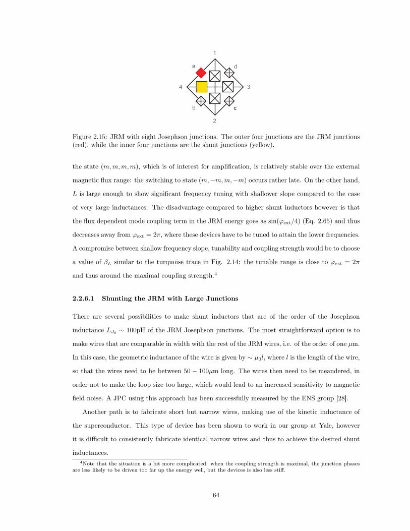
a d
cb
1
2
34
Figure 2.15: JRM with eight Josephson junctions. The outer four junctions are the JRM junctions(red), while the inner four junctions are the shunt junctions (yellow).
the state (m,m,m,m), which is of interest for amplification, is relatively stable over the external
magnetic flux range: the switching to state (m,−m,m,−m) occurs rather late. On the other hand,
L is large enough to show significant frequency tuning with shallower slope compared to the case
of very large inductances. The disadvantage compared to higher shunt inductors however is that
the flux dependent mode coupling term in the JRM energy goes as sin(ϕext/4) (Eq. 2.65) and thus
decreases away from ϕext = 2π, where these devices have to be tuned to attain the lower frequencies.
A compromise between shallow frequency slope, tunability and coupling strength would be to choose
a value of βL similar to the turquoise trace in Fig. 2.14: the tunable range is close to ϕext = 2π
and thus around the maximal coupling strength.4
2.2.6.1 Shunting the JRM with Large Junctions
There are several possibilities to make shunt inductors that are of the order of the Josephson
inductance LJ0∼ 100pH of the JRM Josephson junctions. The most straightforward option is to
make wires that are comparable in width with the rest of the JRM wires, i.e. of the order of one µm.
In this case, the geometric inductance of the wire is given by ∼ µ0l, where l is the length of the wire,
so that the wires need to be between 50 − 100µm long. The wires then need to be meandered, in
order not to make the loop size too large, which would lead to an increased sensitivity to magnetic
field noise. A JPC using this approach has been successfully measured by the ENS group [28].
Another path is to fabricate short but narrow wires, making use of the kinetic inductance of
the superconductor. This type of device has been shown to work in our group at Yale, however
it is difficult to consistently fabricate identical narrow wires and thus to achieve the desired shunt
inductances.4Note that the situation is a bit more complicated: when the coupling strength is maximal, the junction phases
are less likely to be driven too far up the energy well, but the devices is also less stiff.
64

5μm
a)
5μm
b)JRM junction
JRM junctionshunt junction
shunt junction
Figure 2.16: SEM image of two implementations of the JRM with eight junctions: a) Devicefabricated using the Dolan bridge technique. b) Device fabricated using the bridge-free technique.
The strategy taken in this work is to fabricate additional larger Josephson junctions which
shunt the JRM junctions, as shown schematically in Fig. 2.15. This method has the advantage
of reliability and predictability in the fabrication of Josephson junctions with LJ0∼ 100 pH. Two
type of devices were developed and fabricated, one which made use of the Dolan bridge technique
[62] and a second without suspended resist bridge, called the bridge-free technique [63]. These two
type of JRMs are shown in Figs. 2.16 a) and b), respectively. The ratio of the junction areas in a)
is 1:0.3 (5µm2 to 1.5µm2), so that 2βL = 0.6, assuming the ideal case where the junction critical
current scales exactly with the area5 and where the inductances of the connecting wires of the
ring do not significantly contribute to the overall inductance. In this case the crossover as defined
in Eq. 2.85 is expected at ϕcrossoverext = 3.25π. For the junctions in Fig. 2.16 b) the ratio of the
junction areas is 1:0.43 (5.3µm2to 2.3µm2), so that 2βL = 0.87 and the expected crossover is at
ϕcrossoverext = 2.8π.
Figure 2.17 shows the magnetic flux dependence of the resonance frequencies of a JPC (sample
JPXs01) with shunted JRM (nominally identical to device shown in Fig. 2.16 a) ). The three large
lobes centered around Φext = 0,±4 correspond to the state (m,m,m,m), while the two small lobes
correspond to the state (m,−m,m,−m). It is apparent in this figure that 1. the degeneracy was
successfully lifted by shunting the JRM junctions, as there is no hysteresis (data in sub-figure a)
swept upward, in b) swept downward) and 2. that this devices is tunable in frequency over almost
1GHz on the signal port (sub figure a) ). Further, the crossover appears to occur close to ϕext = 3π,
so that the expected value of 2βL = 0.6 cannot be far from the actual value.
Figure 2.18 shows the flux dependence of another JPC with shunted junctions, fabricated this5This is approximately true for junctions of the sizes considered here.
65

7.8
7.6
7.4
7.2
7.0
Freq
uenc
y (G
Hz)
-5 -4 -3 -2 -1 0 1 2 3 4 5Φ/Φ0
5.4
5.2
5.0
4.8Freq
uenc
y (G
Hz)
-5 -4 -3 -2 -1 0 1 2 3 4 5Φ/Φ0
-180-120-60060120180
Phase (deg.)
a)
b)
sweep direction
sweep direction
signal port
idler port
Figure 2.17: Phase response of JPC with shunted JRM for modulated magnetic flux (sampleJPXs01; fabricated with Dolan bridges). No pump power is applied. a) Signal port. The yel-low color indicates the location of the resonator center frequency. The flux is swept upward. b)Idler port. The flux is swept downward.
66

5.8
5.7
5.6
5.5
Freq
uenc
y (G
Hz)
-4 -3 -2 -1 0 1 2 3 4
8.0
7.8
7.6
7.4
Freq
uenc
y (G
Hz)
-4 -3 -2 -1 0 1 2 3 4Φ/Φ0
-180-120-60060120180
Phase (deg.)
a)
b) Φ/Φ0
sweep direction
sweep direction
signal port
idler port
Figure 2.18: Phase response of JPC with shunted JRM for modulated magnetic flux (sampleJPXs01; fabricated with bridge-free technique). No pump power is applied. a) Signal port. Theyellow color indicates the location of the resonator center frequency. The flux is swept upward. b)Idler port. The flux is swept downward. An additional hysteretic state appears.
time with the bridge-free technique (sample JPXs04; nominally identical to device in Fig. 2.16 b) ).
This device again shows three large lobes, and the device is operated in that regime when used as
an amplifier. On the signal port, the frequency tunability is around 300MHz. There are two reasons
for this reduced (yet sufficient) tunability: first, the junctions have a higher critical current density
than the junctions in the device of Fig. 2.176, and thus the junctions overall participate more in
the resonance frequency. And second, an additional state seems to appear, which is hysteretic.
It is possible that this state is due to the fact that the wires connecting the junctions have non-
negligible inductance, as they are only 200nm wide and 20-30nm thick. In future devices fabricated
with the bridge-free technique, care should be taken to increase the wire with and especially the
wire thickness.
6Sample JPXs04 underwent Ar-Ox cleaning before the evaporation step, JPXs01 did not.
67

Chapter 3
Scattering Matrix Description of
Gain and Noise of Parametric
Amplifiers
In this chapter, the scattering matrix description of parametric amplifiers (paramps) is presented,
which allows one to explicitly calculate the gain and noise properties of these devices. The scattering
matrix for the Josephson Parametric Converter (JPC), linking input and output field operators, is
first derived from the Hamiltonian of three harmonic oscillators coupled through only a tri-linear
term XY Z, and under the stiff pump approximation. By introducing flying oscillators and the
two-mode squeezing operator, the same scattering matrix is re-derived and the noise properties
of the JPC are explicitly calculated. The close link between phase-preserving and phase-sensitive
paramps is established, and it is shown how phase-preserving amplifiers can be constructed from
phase-sensitive amplifiers and vice versa. Lastly, the evolution of coherent states is calculated,
showing that those states are a natural basis in which to describe the JPC operation.
3.1 JPC Scattering Matrix
An ideal non-degenerate parametric amplifier is composed of three LC oscillators coupled by a
three-wave mixing term and described by a Hamiltonian of the form (neglecting damping and drive
terms)
68

H0 =Φ2X
2La+
Φ2Y
2Lb+
Φ2Z
2Lc(3.1)
+Q2X
2Ca+Q2Y
2Cb+Q2Z
2Cc
+KΦXΦY ΦZ ,
where ΦX,Y,Z are the generalized flux variables andQX,Y,Z the charge variables [69, 27]. This Hamil-
tonian represents three independent harmonic oscillators with frequencies ωa,b,c = 1/√La,b,cCa,b,c
and characteristic impedances Za,b,c0 =√La,b,c/Ca,b,c, coupled to each other through the three-
wave mixing coefficient K. In general, the modes are described by their (non-degenerate) resonant
frequencies ωa,b,c and (non-overlapping) bandwidths γa,b,c, which for the case ωa < ωb < ωc means
that ωa + γa ωb − γb and ωb + γb ωc − γc. In terms of annihilation operators a, b, and c
associated with each oscillator, the Hamiltonian can be written as
H0 = ~ωaa†a+ ~ωbb†b+ ~ωcc†c (3.2)
+~g3(a+ a†)(b+ b†)(c+ c†),
where the three-wave mixing interaction is now described by the coupling energy ~g3 = KΦ0XΦ0
Y Φ0Z
and Φ0X,Y,Z :=
√⟨0∣∣∣Φ2X,Y,Z
∣∣∣ 0⟩ is the zero-point fluctuation of the flux.
As explained in Ch. 2, in the case of the JPC this tri-linear mixing term is realized by the
Josephson Ring Modulator (JRM). As the generalized fluxes across the JRM represent only a
fraction of the total generalized fluxes ΦX,Y,Z described in Eq. 3.1, the participation ratios pa,b,c ≈
LJo/La,b,c come into play. These participation ratios represent the fraction of the respective mode
energy contained in the JRM. Consequently, the coupling term in the case of the JRM can be
expressed as [27]
g23 =
papbpcωaωbωcEeffJ /~
, (3.3)
where EeffJ is the effectively available Josephson energy, proportional to EJ of the junctions.
With ωc = ωa + ωb and under the rotating wave approximation (RWA) one finally arrives at
HRWA0 = ~ωaa†a+ ~ωbb†b+ ~ωcc†c+ ~g3
(a†b†c+ abc†
). (3.4)
69

This Hamiltonian allows for a photon picture interpretation of the amplification process: the term
a†b†c describes the annihilation of one pump photon at ωc that leads to the creation of a pair
of signal and idler photons at ωa and ωb, respectively. The coherent amplification process (with
non-zero signal or idler inputs) occurs for pump photon fluxes close to but below the threshold
photon flux npoc = γaγbγc/4g23 , which is the regime of interest in this work. Under the stiff pump
approximation (see below) [27], only the term a†b†c enters in the derivation of the JPC scattering
matrix. The hermitian conjugate term abc†, which describes the reverse process of a pair of signal
and idler photons being annihilated to create a pump photon and leads to Coherent Attenuation
(CA), is the subject of Chapter 5.
By adding drive and dissipation to the Hamiltonian of Eq. 3.4, the coupled equations of motion
(quantum Langevin equations) of operators a, b, c can be derived:
d
dta(t) = −iωaa(t)− γa
2a(t)− ig3b
†(t)c(t) +√γaa
in(t) (3.5)
d
dtb(t) = −iωbb(t)−
γb2b(t)− ig3a
†(t)c(t) +√γbb
in(t)
d
dtc(t) = −iωcc(t)−
γc2c(t)− ig3a(t)b(t) +
√γcc
in(t),
where γa,b,c are the mode bandwidths and the ain, bin, cin are related to the input fields ain, bin, cin
through ain(t) := (2π)−1/2´∞
0ain[ω]e−iωtdω and similarly for bin, cin (see Sec. 3.2.1.1 for field
operator properties). When operating the JPC as an amplifier, the regime of interest is where
the pump dynamics do not play a role. The incoming pump photon flux should be orders of
magnitude above the incoming signal and idler photon flux while γc γa,b, i.e. here of the order
of ωc, so that still only few pump photons occupy the pump resonator at any one time. This
is the stiff pump approximation, in which the operator c(t) can be replaced by the average value
〈c(t)〉 =√nce−iωct−ϕp , where nc is the average photon number of the coherent state produced in the
pump resonator. This number is assumed to be constant over time, so that the coupled equations
of motion 3.5 reduce to two equations for signal and idler only. Finally, using Eq. 3.5 together with
resonator input output relations √γaa(t) = ain(t) + aout(t) and similarly for b(t), which link the
mode amplitudes a(t), b(t) to the outside field operators ain/out[ω], bin/out[ω], one arrives at probably
the most important equation describing the JPC, the (reduced) two-port scattering matrix [25, 27]:
70
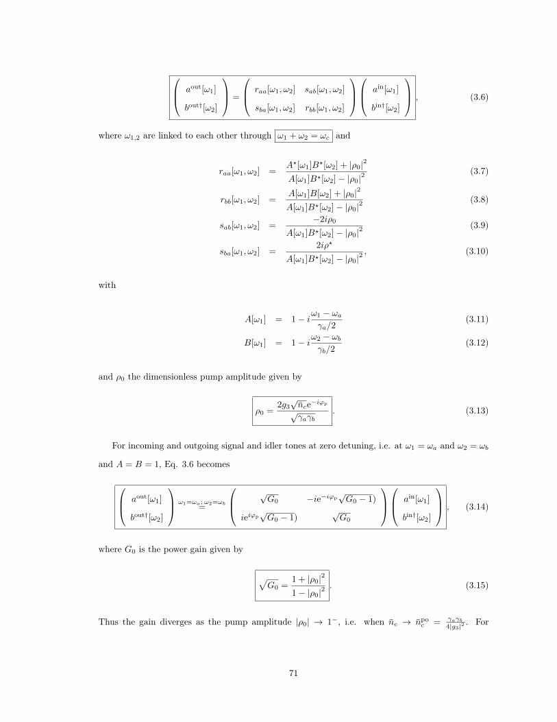
aout[ω1]
bout†[ω2]
=
raa[ω1, ω2] sab[ω1, ω2]
sba[ω1, ω2] rbb[ω1, ω2]
ain[ω1]
bin†[ω2]
, (3.6)
where ω1,2 are linked to each other through ω1 + ω2 = ωc and
raa[ω1, ω2] =A?[ω1]B?[ω2] + |ρ0|2
A[ω1]B?[ω2]− |ρ0|2(3.7)
rbb[ω1, ω2] =A[ω1]B[ω2] + |ρ0|2
A[ω1]B?[ω2]− |ρ0|2(3.8)
sab[ω1, ω2] =−2iρ0
A[ω1]B?[ω2]− |ρ0|2(3.9)
sba[ω1, ω2] =2iρ?
A[ω1]B?[ω2]− |ρ0|2, (3.10)
with
A[ω1] = 1− iω1 − ωaγa/2
(3.11)
B[ω1] = 1− iω2 − ωbγb/2
(3.12)
and ρ0 the dimensionless pump amplitude given by
ρ0 =2g3√nce−iϕp
√γaγb
. (3.13)
For incoming and outgoing signal and idler tones at zero detuning, i.e. at ω1 = ωa and ω2 = ωb
and A = B = 1, Eq. 3.6 becomes
aout[ω1]
bout†[ω2]
ω1=ωa; ω2=ωb=
√G0 −ie−iϕp
√G0 − 1)
ieiϕp√G0 − 1)
√G0
ain[ω1]
bin†[ω2]
, (3.14)
where G0 is the power gain given by
√G0 =
1 + |ρ0|2
1− |ρ0|2. (3.15)
Thus the gain diverges as the pump amplitude |ρ0| → 1−, i.e. when nc → npoc = γaγb4|g3|2
. For
71

large gains√G0 − 1 ≈
√G0 and Eq. 3.14 predicts that the JPC essentially adds signal and idler
amplitudes with power gain G0. When operated as a one-port amplifier, the JPC amplifies the
input with power gain G0 while adding half a photon of noise entering through the idler port and
stemming from the zero point fluctuations of the incoming field bin[ω].
While the frequency dependent scattering matrix of Eq. 3.6 looks rather complicated compared
to the one obtained for zero detuning in Eq. 3.14, for large gains it simply predicts a Lorentzian
shaped (power) gain function at frequencies close to the mode centers ωa,b for both the signal and
the idler port:
G0(∆ω) = G0B2(G0)/4
B2(G0)/4 + ∆ω2, (3.16)
where ∆ω = ω1 − ωa = ωb − ω2 and
B(G0) = B0G−1/20 (3.17)
is the full width at half maximum (i.e. the bandwidth) of the Lorentzian at gain G0, and which is
determined by the pump strength through Eq. 3.15. The constant bandwidth B0 is given by a sort
of average of the signal and idler resonators γa, γb through
B0 =2γaγbγa + γb
, (3.18)
and it is clear from these expressions that the JPC bandwidth B is dominated by the smaller of
the signal and idler resonator bandwidths, and it is thus desirable to make them equal.
Figure 3.1 summarizes how the reduced scattering matrix of Eq. 3.6 couples frequency compo-
nents ω1 and ω2 of the signal and idler fields, respectively, which are linked by ω1 +ω2 = ωc. Figure
3.1 (a) shows the Lorentzian power gain response functions of signal and idler ports together with
all relevant frequency relations and bandwidths. Figure 3.1 (b) shows graphically the frequency
mixing process described by the JPC scattering matrix of Equation 3.6.
3.2 Phase-Sensitive and Phase-Preserving Amplification
Many of properties of the JPC (operated in its amplification mode) can be calculated using its
reduced scattering matrix. It describes how the JPC processes classical signals and allows one to
72

Idler Signal
Pump
ωaωb ωc
ω1ωc−ω1
ωa
ω1
ωb−ωb−ωa
−ω1
ωaωb−ωb−ωa
ω1ωc−ω1−(ωc−ω1)−ω1
ωc
ωc
a)
b)
0
0
0
ω
ω
ω
γb
IN
OUT
γa
ωa + ωb = ωc
Figure 3.1: a) Schematic of JPC operation in frequency space, as could be observed with a com-mercial spectrum or network analyzer. The red and blue Lorentzian shapes represent the powergain response functions of the JPC, centered around the signal and idler center frequencies ωa andωb respectively. The respective dynamical amplifier bandwidths are given by γa and γb. Coloredarrows represent CW tone powers. The pump tone is applied at ωc = ωa + ωb. An applied signaltone at ω1 within the signal bandwidth will be amplified and a further amplified copy will alsoappear at the idler port at ωc − ω1. b) Frequency mixing properties of the JPC, as calculatedby scattering matrix 3.49. Vertical colored arrows represent CW tone amplitudes a† and a etc.,corresponding to positive and negative frequency components. An applied CW tone with frequencyω1 (top half of figure) is represented by its positive and negative frequency components at ±ω1,and leads to amplified CW tones at frequencies ω1 and ωc − ω1 (bottom half of figure), again rep-resented by positive and negative frequency components. The dashed arrows show how the JPCmixes the different frequency components. The purple arrows show the frequency relation betweensignal, idler, and tones. Vertical dashed arrows correspond to amplitude gains
√G0 and diagonal
to amplitude gains√G0 − 1. Noise in the idler port (no applied tone) is mixed in to appear at the
output of both the signal and idler port.
73

calculate statistical properties of e.g. coherent states. In particular, it makes it clear that the
zero-point fluctuation on the idler port is at the origin of the JPC amplifier noise. It also makes
it possible to predict the statistical properties of two-mode squeezed noise produced by the JPC
[70, 71]. The scattering matrix approach further allows one to identify the relationship between
a non-degenerate, phase-preserving paramp such as the JPC and a conceptually closely related
device, the degenerate, phase-sensitive parametric amplifier, of which several different experimental
implementations with superconducting Josephson circuits exist [20, 29, 22, 23]. Before (re-)deriving
the scattering matrix using the two-mode squeezing operator Sab(Λ), it is useful to review some
commutator properties of the signal and idler input annihilation operators ain, bin, derived from
the input field operators ain[ω] and bin[ω], and their corresponding quadrature operators.
3.2.1 Commutation Relations
3.2.1.1 Field Operators
The equations of motion (quantum Langevin equations) of Eq. 3.5 describe the time evolution of
operators a(t), b(t), and c(t), associated with the three LC oscillators of the JPC. At t = 0, a(0) = a,
b(0) = b, and c(0) = c and these operators obey the usual harmonic oscillator commutation relations:
[a, a†] = 1 (3.19)
etc. These standing wave amplitudes link incoming and outgoing field operators ain[ω] (bin[ω] ) and
aout[ω] (bin[ω]) to each other through the oscillator input-output relations
√γaa(t) = ain(t) + aout(t) (3.20)
√γbb(t) = bin(t) + bout(t), (3.21)
where
ain(t) :=1√2π
∞
0
ain[ω]e−iωtdω (3.22)
bin(t) :=1√2π
∞
0
bin[ω]e−iωtdω (3.23)
74

(e.g. see appendix of [27]). Further, these field operators satisfy
[ain(out)[ω], ain(out)[ω′]
]=
[bin(out)[ω], bin(out)[ω′]
]= sgn (ω − ω′) δ (ω + ω′) , (3.24)
and
⟨ain[ω], ain[ω′]
⟩= 2N in
a
(ω − ω′
2
)δ (ω + ω′) (3.25)
⟨bin[ω], bin[ω′]
⟩= 2N in
b
(ω − ω′
2
)δ (ω + ω′) , (3.26)
where
N ina,b(ω) =
sgn(ω)
2coth
(~ω
2kBT
)+ 2πna,b [δ (ω − ω1,2) + δ (ω + ω1,2)] (3.27)
is the photon spectral density of the incoming fields, T is the temperature, and na,b is the photon flux
of an applied tone at frequency ω1,2. Note that ain(out)[ω]† = ain(out)[−ω], bin(out)[ω]† = bin(out)[−ω].
3.2.1.2 Flying Oscillators
From the field operators, flying oscillator amplitudes can be defined using Shannon wavelets [72, 73]:
ain(out),n :=1√κ
ωa+κ/2ˆ
ωa−κ/2
ain(out)[ω]e+iω nκ dω (3.28)
bin(out),n :=1√κ
ωb+κ/2ˆ
ωb−κ/2
bin(out)[ω]e+iω nκ dω, (3.29)
(3.30)with κ γa, γb . Using 3.24 it is easy to show that
[ain(out),n, a
†in(out),n
]=
[bin(out),n, b
†in(out),n
]=
1
κ
∞
−∞
∞
−∞
sgn (ω + ω′) δ (ω − ω′) e+i(ω−ω′)nκ dωdω′
= 1. (3.31)
In the following, the index n will be dropped to simplify the discussion. Note also that this discussion
75

is limited to flying oscillators defined at resonance, i.e. around ωa and ωb. This could be further
generalized to off-resonance frequencies ωa − δω and ωb + δω, as schematically done in Fig. 3.1.
The commutation relations of ain and bin are
[ain, a†in] = [bin, b
†in] = 1 (3.32)
[a(†)in , b
(†)in ] = 0. (3.33)
The quadrature operators I and Q are defined as
Iain :=ain + a†in
2(3.34)
Qain :=ain − a†in
2i(3.35)
Ibin :=bin + b†in
2(3.36)
Qbin :=bin − b†in
2i, (3.37)
and from this follows that they obey the following commutation relations:
[Iain , Qain ] = [Ibin , Qbin ] =i
2(3.38)
and
[Iain , Ibin ] = [Qain , Qbin ] = [Ia(b)in , Qb(a)in ] = 0. (3.39)
Note that operators I and Q are hermitian, i.e. I† = I and Q† = Q and the corresponding
eigenvalues are thus real. The annihilation operators ain and bin can be expressed in terms of I and
Q as
ain = Iain + iQain (3.40)
bin = Ibin + iQbin . (3.41)
76

3.2.2 Two-Mode Squeezing Operator and JPC Scattering Matrix
The mode coupling term g3(a†b†c+ abc†) in the JPC Hamiltonian (Eq. 1.7) leads to an evolution
operator of the form UJPC = exp[za†b† − h.c.], where z ∈ C. The evolution of incoming signal and
idler fields |Ψ〉in is described by S†ainbin(Λ) |Ψ〉in, where Sab(Λ) is the two-mode squeezing operator ,
defined as
Sab(Λ) := exp[Λa†b† − Λ?ab] , (3.42)
with Λ ≡ λeiϕ, and λ, ϕ ∈ R. Note that the phase ϕ is directly related to the pump phase ϕp
through ϕ = −ϕp + π/2, whereas λ = ln(√G0 +
√G0 − 1) is a measure of the JPC power gain G0.
The two-mode squeezing operator is unitary:
S−1ab (Λ) = S†ab(Λ) = Sab(−Λ). (3.43)
The Baker-Hausdorff formula
eABe−A = B + [A,B] +1
2![A, [A,B]] + ... (3.44)
together with the commutation relations of Equation 3.32 can then be used to calculate the output
fields as a function of the input fields:
aout = Sainbin(Λ)ainS†ainbin
(Λ) (3.45)
= ain +(−Λ)
1!b†in +
(−Λ)(−Λ?)
2!ain +
(−Λ)(−Λ?)(−Λ)
3!b†in + ... (3.46)
=
( ∞∑n=0
|Λ|2n
(2n)!
)ain +
(−Λ)
|Λ|
( ∞∑n=0
|Λ|2n+1
(2n+ 1)!
)b†in (3.47)
= cosh(|Λ|)ain +(−Λ)
|Λ|sinh(|Λ|)b†in, (3.48)
and similarly for b†out, so that one finally arrives at the reduced JPC scattering matrix
aout
b†out
=
cosh(λ) −eiϕ sinh(λ)
−e−iϕ sinh(λ) cosh(λ)
ain
b†in
, (3.49)
where cosh(λ) ≡√G0, sinh(λ) ≡
√G0 − 1 and λ ≡ |Λ|. Note that since Sainbin(Λ) is unitary, aout
77
and bout obey the same commutation relations as ain and bin:
[aout, a†out] = [bout, b
†out] = 1. (3.50)
Equation 3.49 also implies that Sainbin(Λ) ≡ Saoutbout(Λ).
Alternatively, the operation of the JPC can be described through the transformation of the
quadrature operators I and Q, which can be easily calculated using the scattering matrix in Equa-
tion 3.49 together with definitions of Equations 3.34, 3.35, 3.36, 3.37:
Iaout ≡ aout+a†out
2 = cosh(λ)Iain + sinh(λ)Ib′in (3.51)
Qaout ≡ aout−a†out2i = cosh(λ)Qain − sinh(λ)Qb′in (3.52)
Ib′out≡ b′out+b
′†out
2 = cosh(λ)Ib′in + sinh(λ)Iain (3.53)
Qb′out≡ b′out−b
′†out
2i = cosh(λ)Qb′in − sinh(λ)Qain , (3.54)
where b′in = e−i(ϕ+π)bin, and b′out = e−i(ϕ+π)bout are simply the phase shifted incoming and outgoing
idler wave annihilation operators. This phase shift corresponds in I −Q space to a rotation by an
angle ϕ+ π:
Ib′in(out)
Qb′in(out)
:=
cos(ϕ+ π) sin(ϕ+ π)
− sin(ϕ+ π) cos(ϕ+ π)
Ibin(out)
Qbin(out)
. (3.55)
This means that the effect of the pump phase on the idler field is equivalent to phase-delaying
sections of loss-less transmission lines on the idler input and output ports (i.e. redefining the idler
reference planes) with delay ϕ+π and −(ϕ+π) respectively. This justifies setting −eiϕ != 1, as done
later in this chapter to simplify the discussion. Of course this makes sense only in situations when
the pump phase is kept constant. Note again that the JPC preserves the commutation relations of
I and Q (Equation 3.38), i.e. [Iaout , Qaout ] = i2 etc.
Both the scattering matrix of Equation 3.49 and the transformation rules for the field quadra-
tures of Equations 3.51 and 3.52 reveal how the JPC amplifies signal field amplitudes and quadra-
tures with amplitude gain cosh(λ) ≡√G0 in the absence of incoming idler fields. Further it becomes
clear that the origin of amplifier noise is the incoming noise on the idler port which is amplified by
78

a factor sinh(λ) ≡√G0 − 1 ≈
√G0 ≡ cosh(λ) for large gains.
3.2.3 One-Mode Squeezing Operator and JBA-paramp Scattering Ma-
trix
There is a strong connection between a non-degenerate, phase-preserving paramp performing three-
wave mixing operations, such as the JPC and a degenerate, phase-sensitive paramp performing
four-wave mixing operations, such as the Josephson Bifurcation Amplifier (JBA) (in its paramp
mode of operation). In fact, as will be shown below, a JPC can be constructed with two JBAs, and
a JBA can be constructed with one JPC. It is useful to review the JBA scattering matrix, which
can be calculated similarly to the JPC scattering matrix using the one-mode squeezing operator
Sa(ξ) := exp[ξ
2a†a† − ξ?
2aa] , (3.56)
with ξ ≡ |ξ|eiϕξ ,1 where ϕξ again is related to the pump phase ϕp, since ϕξ = −2ϕp + π/2. The
one-mode squeezing operator is also unitary:
S−1a (ξ) = S†a(ξ) = Sa(−ξ). (3.57)
Using the commutation relations [a†ina†in, ain] = [a†in, ainain]† = −2a†in together with Equation 3.44
yields
aout = Sain(ξ)ainS†ain
(ξ) (3.58)
= cosh(|ξ|)ain −ξ
|ξ|sinh(|ξ|)a†in, (3.59)
so that the phase-sensitive degenerate paramp (e.g.JBA) is described by
aout = cosh(|ξ|)ain − eiϕξ sinh(|ξ|)a†in , (3.60)
and cosh(|ξ|) ≡√G0 is the amplitude gain, and sinh(|ξ|) ≡
√G0 − 1. At first glance, Equations
3.49 and 3.60 look very similar, a closer look however reveals that the signal output field in the1Note that ξ is used as a parameter in the general one-mode squeezing operator, while λ is the parameter used
in the two-mode squeezing operator. As will be shown below, the two-mode squeezing operation can be rewritten astwo one-mode squeezing operations, with |ξ| = |λ|.
79
phase-sensitive amplifier depends only on the signal input field and its conjugate, and no mixing
with an idler field occurs. The consequences of this relationship becomes much clearer when looking
at the transformation rules for the field quadratures I and Q:
Iout ≡ aout + a†out2
= (cosh(|ξ|)− cos(ϕξ) sinh(|ξ|)) Iin − (sin(ϕξ) sinh(|ξ|))Qin (3.61)
Qout ≡ aout − a†out2i
= − (sin(ϕξ) sinh(|ξ|)) Iin + (cosh(|ξ|) + cos(ϕξ) sinh(|ξ|))Qin, (3.62)
where Iin ≡ain+a†in
2 and Qin ≡ain−a†in
2i . Again, a change in reference plane greatly simplifies the
above expression, this time rotating both the input and output fields by the same phase +ϕξ2 :
I ′in(out)
Q′in(out)
:=
cos(ϕξ2 ) sin(
ϕξ2 )
− sin(ϕξ2 ) cos(
ϕξ2 )
Iin(out)
Qin(out)
, (3.63)
or equivalently
a′in(out) := e−iϕξ2 ain(out). (3.64)
This finally leads to the following transformation rules for the quadrature operators:
I ′out = e−|ξ|I ′in and Q′out=e+|ξ|Q′in . (3.65)
This means that a phase-sensitive degenerate paramp amplifies one quadrature (here Q) by a
factor e+|ξ| ≡√G0 +
√G0 − 1, while deamplifying the conjugate quadrature (here I) by e−|ξ| ≡
√G0 −
√G0 − 1. Thus signals with phase +ϕξ/2 + π/2 + nπ (n ∈ Z) are amplified, while signals
with phase +ϕξ/2 + nπ are deamplified. Of course one can formally interchange the amplified and
deamplified quadratures (I ↔ Q) in Equations 3.65 by an appropriate redefinition of the reference
plane (i.e. rotation of the incoming and outgoing fields) or by setting the pump phase to ϕξ = π in
Equations 3.61,3.62.
3.2.3.1 Implementations of phase-sensitive amplifiers
Phase-sensitive parametric amplification is typically achieved with frequency degenerate amplifiers,
but can also be done with non-degenerate amplifiers such as the JPC, as shown in Ch. 5. Several
different implementations with Josephson devices exist, mainly differing in the frequency of the
applied continuous wave (CW) pump tone. They all have in common that only one relevant resonant
80

Pump
Idler Signal
ωa
a)
2ωa
ω12ωa-ω1
Pump
Idler Signal
ωa
b)
ω12ωa-ω1
0 ω0ω
Pump 2
Idler Signal
ωa
c)
ω12ωa-ω1
ω0
Pump 1
ωa+∆ωa-∆
Figure 3.2: Different implementations of degenerate parametric amplifiers. a) Pump frequency attwice the amplification center frequency ωa. This type of device corresponds to a non-linearity ofthe form X2Z (χ(2)-medium in optics) and has been implemented with Josephson junctions [22].b) Pump frequency at the amplification center frequency ωa. Several implementations of this X4
type non-linearity (χ(3)-medium in optics) have been achieved with superconducting circuits, e.g.JBA-paramp [23], Josephson junction array paramp [20], and non-linear CPW resonators [29]. c)Two pumps at equal distance and on opposite sides of center frequency ωa. This operation can beachieved by e.g. applying two pumps in a JBA device [74].
mode exists. Figure 3.2 summarizes the operation of some degenerate paramps in frequency space.
3.2.3.2 Phase-preserving operation of a degenerate amplifier
One point of confusion that regularly arises in the discussion of frequency degenerate amplifiers is
their operation as phase-preserving amplifiers, similar to the operation of the JPC. The natural
mode of operation of degenerate amplifiers is as phase-sensitive amplifiers, as described by the
scattering matrix of equation 3.60. In this case, the signal is centered around the band center of
the amplifier, typically defined by the frequency of the CW pump tone (or half the frequency, see
Figure 3.2). Should however the signal be injected asymmetrically on only one side of the amplifier
band, then the device operates as a phase-preserving amplifier obeying Equation 3.49, and an idler
field appears on the opposite side of the signal band. This case is schematically described in Figure
3.3.
81

ωa
ω1
-ωa
2ωa
2ωa
0 ω
IN
OUT
ωa-ωa 0 ω
-ω1
-ω1 -(2ωa-ω1) 2ωa-ω1 ω1
Figure 3.3: Operation of a degenerate paramp such as the JBA operated in the phase-preservingmode, represented in frequency space. Colored arrows represent wavelet amplitudes a† and a, whengeneralizing the flying oscillator definition to include frequencies off-resonance, and correspondingto positive and negative frequency components. For orientation, Lorentzian shapes representingamplifier power gain response functions are also shown. Blue represents the signal, red the idler.Top: CW tone with frequency ω1 (represented by its positive and negative frequency components)injected on the signal side of the amplifier center frequency ωa. Bottom: Output amplitudes presentat both signal and idler sides. Dashes arrows show direction of frequency mixing. Purple arrowshows frequency relation between pump, signal, and idler tones.
82

3.2.4 Common and Differential Mode Representation: Link Between
JPC and JBA-Paramp
As will be shown now, there is a close relationship between the two-mode JPC and the one-mode
JBA. To simplify the discussion it will be assumed that -eiϕ=1 in the JPC scattering matrix,
which, as mentioned above can be achieved by choosing the correct pump phase or by redefining
the idler field reference planes through rotations, so that Equation 3.49 becomes
aout
b†out
=
cosh(λ) sinh(λ)
sinh(λ) cosh(λ)
ain
b†in
. (3.66)
Describing a phase-preserving parametric amplifier in terms of its signal and idler modes is natu-
rally useful when operating it as a signal amplifier while disregarding the idler port output. This
representation does not however make it easy to identify the correlations between signal and idler
outputs. To reveal those correlations, common and differential modes will now be introduced:
aΣin(out) : =ain(out) + bin(out)√
2(3.67)
a∆in(out) : =ain(out) − bin(out)√
2, (3.68)
and in terms of the quadrature operators
IΣin(out) :=Iain(out) + Ibin(out)√
2(3.69)
QΣin(out) :=Qain(out) +Qbin(out)√
2(3.70)
I∆in(out) :=Iain(out) − Ibin(out)√
2(3.71)
Q∆in(out) :=Qain(out) −Qbin(out)√
2. (3.72)
These definitions assure that the usual commutation relations still hold, namely [aΣ(∆)in , a†Σ(∆)in
] =
1, [a(†)Σin, a
(†)∆in
] = 0, [IΣ(∆)in , QΣ(∆)in ] = i/2, [IΣin , I∆in ] = 0 etc. and similarly for Σout and ∆out.
This leads to the following
alternative formulation of the JPC scattering matrix :
83
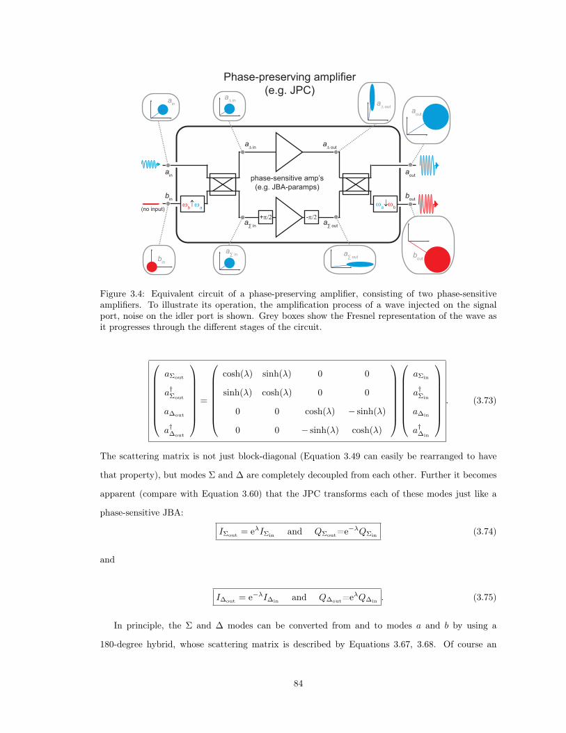
+π/2
Phase-preserving amplifier(e.g. JPC)
ωb↑ωa ωa↓ωb
phase-sensitive amp’s(e.g. JBA-paramps)
-π/2
ain
bin bout
aout
a∆ in
a∑ in
a∆ out
a∑ out
bout
aout
a∆ out
a∑ out
a∆ inain
bin
a∑ in
(no input)
Figure 3.4: Equivalent circuit of a phase-preserving amplifier, consisting of two phase-sensitiveamplifiers. To illustrate its operation, the amplification process of a wave injected on the signalport, noise on the idler port is shown. Grey boxes show the Fresnel representation of the wave asit progresses through the different stages of the circuit.
aΣout
a†Σout
a∆out
a†∆out
=
cosh(λ) sinh(λ) 0 0
sinh(λ) cosh(λ) 0 0
0 0 cosh(λ) − sinh(λ)
0 0 − sinh(λ) cosh(λ)
aΣin
a†Σin
a∆in
a†∆in
. (3.73)
The scattering matrix is not just block-diagonal (Equation 3.49 can easily be rearranged to have
that property), but modes Σ and ∆ are completely decoupled from each other. Further it becomes
apparent (compare with Equation 3.60) that the JPC transforms each of these modes just like a
phase-sensitive JBA:
IΣout = eλIΣin and QΣout=e−λQΣin (3.74)
and
I∆out = e−λI∆in and Q∆out=eλQ∆in . (3.75)
In principle, the Σ and ∆ modes can be converted from and to modes a and b by using a
180-degree hybrid, whose scattering matrix is described by Equations 3.67, 3.68. Of course an
84

Phase-sensitive amplifier(e.g. JBA-paramp)
ωb↑ωaωa↓ωb
phase-preserving amp (e.g. JPC)
ain
bin bout
aout
a∆ in a∆ out
50Ω 50Ω
signalidler
ain
bin
a∆ in
bout
aout
a∆ out
Figure 3.5: Equivalent circuit of a phase-sensitive amplifier, consisting of one phase-preservingamplifier. The phase-preserving amplifier is shown with two ports, one for the idler and one for thesignal wave, generally at different frequencies ωa > ωb. Grey boxes show the Fresnel representationof a wave as it progresses through the different stages of the circuit.
additional step would be necessary to convert modes a and b to the same frequency. This can be
achieved by employing additional JPCs in the noise-less frequency-conversion mode [75]. Figure
3.4 shows how to experimentally implement a phase-preserving JPC described by the scattering
matrix of Equations 3.49 and 3.73 with two phase-sensitive JBA paramps operating at the same
frequency, and both described by Equation 3.60, i.e. both fed with the same pump phase. The
two phase-shifting elements before and after the bottom JBA rotate the axis of amplification from
the I quadrature to the Q quadrature. Note that all elements of the circuit can be implemented
with dispersive elements, so that no additional noise enters the system. In particular the frequency
conversion ωa ↔ ωb can be achieved noise-free with the JPC in its gain-less conversion mode of
operation. The Fresnel representations of the wave as it progresses through the different stages of
the circuit will be explained in more detail below. It is noteworthy that the noise ellipses in the top
and bottom branches are tightly correlated.
The scattering matrix of Equation 3.73 reveals further how the JPC can be operated in phase-
sensitive mode. To achieve this, a signal wave has to be split into signal and idler waves through
a 180-degree hybrid, which are then injected into the JPC and then recombined using another
180-degree hybrid. Again two noise-less frequency conversion steps are necessary, and can be
85

implemented with JPCs in conversion mode. This operation is shown in Figure 3.5. Note that the
matched termination at the input of the first hybrid will emit only quantum noise, provided the
device is operated at low temperature (kBT ~ωa,b). This noise has no effect on the noise-less
amplification along the amplification axis (here the Q quadrature), since it appears at both the
signal and idler outputs and is ultimately canceled out through interference at the last hybrid. The
axis of amplification is determined by the pump phase of the JPC.
It is also possible to cascade two JPCs, connecting the two signal ports and the two idler ports
together and injecting and monitoring the fields on the signal port for instance. The first JPC then
creates a copy of the signal on the idler port and the state of the fields is similar to the state right
before the JPC in Fig. 3.5. There is however one important distinction to the case depicted in Fig.
3.5, as seen later in Eq. 5.9: the created idler tone is going to be phase-conjugated to the signal
tone, so that all signal phase information will be lost in the two JPC process. The amplification
process is still going to be phase-sensitive, but with respect to the difference of the two pump phases
of the two amplification stages. It is thus important that the frequency conversion stage described
in Fig. 3.5 does not phase-conjugate the signal.
In degenerate parametric amplifiers, the phase-sensitivity is sometimes measured by amplitude
modulating a signal, creating two sidebands around the center frequency of the amplifier (e.g.[22]).
The two created sideband tones are then phase-conjugated and the amplifier is sensitive to the
relative phase between the carrier and the pump, but insensitive to the original signal phase.
3.2.5 Signal and Noise Properties: Averages and Standard Deviations
Now that quadrature transformation rules for both the JPC and the JBA have been established
in Equations 3.51, 3.52, 3.65 it is time to investigate how input signals are transformed in general,
by looking at their expectation values E and variances D2 while assuming that no idler inputs are
present (in the JPC case). To simplify the discussion, the ′ symbols will be dropped in the following
and it will be assumed that the pump phases have been chosen appropriately 2.
Before looking at the signal output, it is useful to review some expectation values given the
quadrature operator properties. The length of the Fresnel vector of a signal (input or output, since
they obey the same commutation relations) can be expressed through the quadratures by2Since only noise is presented to the idler port, the above result will hold true for any pump phase.
86

√〈I〉2 + 〈Q〉2 =
√⟨a+ a†
2
⟩2
+
⟨a− a†
2i
⟩2
(3.76)
=√〈a〉 〈a†〉 (3.77)
= |〈a〉| , (3.78)
where 〈X〉 ≡ E(X) is the expectation value. As expected, the length of the Fresnel vector is given by
the modulus of the average amplitude. The standard deviation of each quadrature can be expressed
as3
D2(I) =⟨I2⟩− 〈I〉2 (3.79)
=
⟨(a+ a†
2
)2⟩−⟨a+ a†
2
⟩2
(3.80)
=1
4
[⟨a2 + a†2 + aa† + a†a
⟩− 〈a〉2 −
⟨a†⟩2 − 2 〈a〉
⟨a†⟩]
(3.81)
=1
4
[1 + D2(a) + D2(a†) + 2Cov(a†, a)
], (3.82)
and similarly
D2(Q) =⟨Q2⟩− 〈Q〉2 (3.83)
=1
4
[1− D2(a)− D2(a†) + 2Cov(a†, a)
], (3.84)
where Cov(X,Y ) := E ((E(X)−X) (E(Y )− Y )) is the covariance.
The mean-square fluctuation of a can be defined by
|D|2 (a) :=1
2
⟨aa† + a†a
⟩− 〈a〉
⟨a†⟩
(3.85)
≡ D2(I) + D2(Q). (3.86)
An important case is that of coherent states, where D2|α〉(a) = D2
|α〉(a†) = Cov|α〉(a†, a) = 0:
3D2(O) is used to designate the variance of observable O, while σ2 is used to represent a particular value of thevariance.
87
D2|α〉(I) = D2
|α〉(Q) =1
4, and |D|2|α〉 (a) =
1
2(3.87)
which means that the mean-square fluctuation of a corresponds to half a photon in energy.
3.2.5.1 JPC
When operating the JPC as an amplifier, typically only signal waves are injected into the device
while noise is present on the idler port. An input signal represented by a Fresnel vector with
quadratures 〈Iain〉 and 〈Qain〉 and variances D2(Iain) = D2(Qain) and no input on the idler port
(〈Qbin〉 = 〈Qbin〉 = 0 and D2(Ibin)=D2(Qbin)) is transformed according to the JPC scattering matrix
given in Equations 3.66, 3.51, 3.52. The output quadratures then become
〈Iaout〉 =√G0 〈Iain〉+
√G0 − 1 〈Ibin〉 (3.88)
〈Ibin〉=0=
√G0 〈Iain〉 (3.89)
〈Qaout〉 =√G0 〈Qain〉 −
√G0 − 1 〈Qbin〉 (3.90)
〈Qbin〉=0=
√G0 〈Qain〉 (3.91)
so that for the output amplitude one finds
√〈Iaout〉
2+ 〈Qaout〉
2=
√G0 〈Iain〉
2+ (G0 − 1) 〈Ibin〉
2+G0 〈Qain〉
2+ (G0 − 1) 〈Qbin〉
2
=
√G0 |〈ain〉|2 + (G0 − 1) |〈bin〉|2 (3.92)
〈Ibin〉=〈Qbin〉=0=
√G0
√〈Iain〉
2+ 〈Qain〉
2 (3.93)
⇔ |〈aout〉| =√G0 |〈ain〉| . (3.94)
Equations 3.89, 3.91, 3.94 justify the appellation “phase-preserving” amplifier: both quadratures
are amplified by the same factor so that the phase is preserved in the amplification process, and
signals are amplified by an amplitude gain√G0. The noise properties of the JPC can be calculated
using the scattering matrix:
88

D2(Iaout) = G0D2(Iain) + (G0 − 1)D(Ibin) + 2√G0
√G0 − 1 〈IainIbin〉 (3.95)
〈IainIbin〉=0= G0D2(Iain) + (G0 − 1)D2(Ibin), (3.96)
and
D2(Qaout) = G0D2(Qain) + (G0 − 1)D2(Qbin)− 2√G0
√G0 − 1 〈QainQbin〉(3.97)
〈QainQbin〉=0= G0D2(Qain) + (G0 − 1)D2(Qbin), (3.98)
where the fact that Iain , Ibin (Qain , Qbin) commute and are independent has been used. For large
gains (G0 1) and only quantum noise on the idler port (see Equation 3.87) one arrives at the
important result:
D2(Iaout) = D2(Qaout) = G0
(σ2I,Q +
1
4
)and |D|2 (aout) = G0
(σ2a +
1
2
), (3.99)
where the signal input noise is assumed to be isotropic D2(Iain) = D2(Qain) =: σ2I,Q and σ2
a :=
|D|2 (ain) = 2σ2I,Q
4. The added noise of the JPC thus corresponds to only half a photon, which
is the minimum of added amplifier noise for a linear phase-preserving amplifier [5]. The JPC
minimally degrades the intensity signal-to-noise ratio (SNR) of input signals from |〈ain〉|2 /σ2a to
|〈ain〉|2 /(σ2a + 1
2
). Figure 3.6 (top) shows this behavior graphically.
3.2.5.2 JBA-Paramp
The calculation of signal and noise properties of the output of a phase-sensitive paramp is partic-
ularly simple, using Equations 3.65. Again, it will be assumed (for legibility and without loss of
generality) that the input and output fields are defined such that the ′-symbols in Equations 3.65
can be dropped (equivalently, ϕξ can be set to zero in Equations 3.61, 3.62). Then an input field
defined by 〈Iin〉 and 〈Qin〉 and variances D2(Iin) = D2(Qin) =: σ2I,Q leads to output field quadratures
4More precisely, the error ellipse is circular, i.e. D2(ain) = 0 [5].
89

〈Iout〉 = e−|ξ| 〈Iin〉 (3.100)
〈Qout〉 = e+|ξ| 〈Qin〉 . (3.101)
Thus the field is simply amplified by a factor e+|ξ| in the Q quadrature while deamplified by a
factor e−|ξ| in the I quadrature. It is clear that this amplifier is strongly phase-dependent, and for
large gains (e+|ξ| 1) all phase information is nearly erased. The noise properties of these devices
are also easily calculated:
D2(Iout) = e−2|ξ|D2(Iin) (3.102)
= e−2|ξ|σ2I,Q (3.103)
D2(Qout) = e+2|ξ|D2(Qin) (3.104)
= e+2|ξ|σ2I,Q. (3.105)
Noise (variance) in the I quadrature is squeezed by the same factor e+2|ξ| as it is amplified in
the Q quadrature. The SNR of the quadratures remains unchanged, since the output intensity
SNR of the quadratures stays the same as the input SNR: 〈Iout〉2 /D2(Iout) = 〈Iin〉2 /σ2I,Q and
〈Qout〉2 /D2(Qout) = 〈Qin〉2 /σ2I,Q. Figure 3.6 (bottom) graphically shows this phase-sensitive am-
plification process.
3.2.6 Evolution of Coherent States
In the following, the evolution of coherent states UJPC |α, β〉in will be studied explicitly, where
|α, β〉in describes coherent states α and β in the incoming signal and idler flying oscillator modes
described above. The resulting state is described here in the same Hilbert space as the initial state,
namely in that of the incoming flying oscillators.
Using the displacement operator
Dain (α) ≡ eαa†in−α
?ain Eq. 3.44= eαa
†ine−α
?aine−|α|2
2 , (3.106)
90

I
Q
|‹ain›|
I
Q
√G0•|‹ain›|
√G0•σI2+(G0-1)•1/4
I
Q
|‹Iin›|
|‹Qin›|
I
Q
e+λσI
e+λ|‹Iin›|
e-λ|‹Qin›| e-λσQ
phase-preserving amp.
phase-sensitive amp.
σI
σQ
σI
σQ
√G0•σQ2+(G0-1)•1/4
Figure 3.6: Fresnel vector representation of quasi-coherent signals and their transformation throughquantum-limited paramps. Top: The phase-preserving operation of a quantum-limited paramp suchas the JPC will amplify both field quadratures I and Q equally, so that the output phase is the sameas the input phase. The added noise corresponds to half a photon at high gains when referred backto the input. Bottom: The phase-sensitive operation of a quantum-limited paramp amplifies onequadrature (here I) while deamplified the other quadrature (here Q). The SNR of either quadratureremains unaffected by the amplification process.
91

and similarly for bout, the state of the outgoing signal and idler modes can be written as 5
UJPC |α, β〉in = S†ab (Λ) |α, β〉in (3.107)
= S†ab (Λ)Dain (α)Dbin (β) |0, 0〉in (3.108)
= S†ab (Λ)Dain (α)Sab (Λ)︸ ︷︷ ︸ S†ab (Λ)Dbin (β)Sab (Λ)︸ ︷︷ ︸ S†ab (Λ) |0, 0〉in︸ ︷︷ ︸,(3.109)and the first two terms are just transformations of the displacement operators, using the inverse
scattering matrix of Eq. 3.49:
S†ab (Λ)Dain (α)Sab (Λ) = eαS†ab(Λ)a†inSab(Λ)−α?S†ab(Λ)ainSab(Λ) (3.110)
Eq. 3.49= eα cosh(λ)a†in−α
?cosh(λ)ain (3.111)
e−α?eiϕ sinh(λ)b†in+αe−iϕ sinh(λ)bin
= Dain (α cosh(λ))Dbin
(−α?eiϕ sinh(λ)
)(3.112)
where Λ ≡ λeiϕ. This is exactly the result one would find using the scattering matrix for a classical
field α in the signal port. Making use of the fact that two consecutive displacements can be written
as
Dain (α)Dain (α′) = eiIm[αα′?]Dain (α+ α′) , (3.113)
the first two terms in Eq. 3.109 become
S†ab (Λ)Dain (α)Dbin (β)Sab (Λ) = S†ab (Λ)DaΣin
(α+ β√
2
)Da∆in
(α− β√
2
)Sab (Λ) (3.114)
= Dain
(α cosh(λ)− β?eiϕ sinh(λ)
)⊗Dbin
(β cosh(λ)− α?eiϕ sinh(λ)
).
Again, the JPC scattering matrix reappears. Note that the phase factors of Eq. 3.113 exactly
cancel. So finally, the evolution of coherent states can be written as5The † in the two-mode squeezing operator follows from the choice of definition 3.45.
92
UJPC |α, β〉in = Dain
(α cosh(λ)− β?eiϕ sinh(λ)
)(3.115)
⊗Dbin
(β cosh(λ)− α?eiϕ sinh(λ)
)⊗S†ab (Λ) |0, 0〉in .
This result is quite remarkable and shows that coherent states are the natural basis in which to
describe the JPC operation. Coherent states almost transform as predicted by the (semi-)classical
scattering matrix of Eq. 3.49: the displacement operators transform according to the scattering
matrix, while additionally the vacuum state undergoes two-mode squeezing. Note that the case
where the signal and idler input states are the vacuum state is sometimes also called spontaneous
parametric down-conversion [76] or parametric fluorescence. Two-mode squeezing of the vacuum
state with the JPC was experimentally observed in [70, 71].
Before looking at a more specific case, consider the change of basis from a, b to Σ, ∆ as in Eqs.
3.67, 3.68:
Dain (α)Dbin (β) = DaΣin
(α+ β√
2
)Da∆in
(α− β√
2
). (3.116)
Further, the two-mode squeezing operator can be decomposed into two one-mode squeezing opera-
tors:
Sab (Λ) = eΛa†inb†in−Λ?ainbin (3.117)
= eΛ2 a†Σin
a†Σin−Λ?
2 aΣinaΣin (3.118)
⊗e−Λ2 a†∆in
a†∆in−−Λ?
2 a∆ina∆in (3.119)
= SΣ (Λ)S∆ (−Λ) , (3.120)
where SΣ(∆) (ξ) := eξ2a†Σ(∆)in
a†Σ(∆)in
− ξ?
2 aΣ(∆)inaΣ(∆)in is the one-mode squeezing operator. Then
S†ab (Λ)Dain (α)Sab (Λ) = DaΣin
(α cosh(λ)− α?eiϕ sinh(λ)√
2
)(3.121)
⊗Da∆in
(α cosh(λ) + α?eiϕ sinh(λ)√
2
), (3.122)
93

and
S†ab (Λ)Dain (α)Dbin (β)Sab (Λ) = DΣin
(α+ β√
2cosh(λ)− α? + β?√
2eiϕ sinh(λ)
)(3.123)
⊗D∆in
(α− β√
2cosh(λ)− α? − β?√
2eiϕ sinh(λ)
).(3.124)
Finally the result of Eq. 3.115 can be expressed as
UJPC |α, β〉in = DΣin
(α+ β√
2cosh(λ)− α? + β?√
2eiϕ sinh(λ)
)(3.125)
⊗D∆in
(α− β√
2cosh(λ)− α? − β?√
2eiϕ sinh(λ)
)⊗S†Σ (Λ)S†∆ (−Λ) |0, 0〉in .
Again, this is the result expected from the (semi-)classical scattering matrix in Eq. 3.73, with
the addition of the one-mode squeezing of both signal and idler vacuum states.
3.2.6.1 Coherent Attenuation
The case of balanced input coherent states (α = |α|e−iϕS , β = |α|e−iϕI) can easily be analyzed
using Eq. 3.115:
UJPC∣∣|α|e−iϕS , |α|e−iϕI
⟩in = Dain
(|α|e−iϕS
(cosh(λ)− ei(ϕS+ϕI+ϕ) sinh(λ)
))(3.126)
⊗Dbin
(|α|e−iϕI
(cosh(λ)− ei(ϕS+ϕI+ϕ) sinh(λ)
))⊗S†ab (Λ) |0, 0〉in ,
which, in terms of the displacement operators, is the same result found in Eq. 5.9:
94
UJPC∣∣|α|e−iϕS , |α|e−iϕI
⟩in = (3.127)
Dain
(|α|e−i(ϕS+γ)
√e2λ sin2
(ϕS + ϕI + ϕ
2
)+ e−2λ cos2
(ϕS + ϕI + ϕ
2
))
⊗Dbin
(|α|e−i(ϕI+γ)
√e2λ sin2
(ϕS + ϕI + ϕ
2
)+ e−2λ cos2
(ϕS + ϕI + ϕ
2
))⊗S†ab (Λ) |0, 0〉in ,
with ϕ ≡ −ϕp + π/2, and γ being the phase of the complex number cosh(λ)− ei(ϕS+ϕI+ϕ) sinh(λ)
(λ ∈ R+). Thus for nonlinear phases ϕS + ϕI + ϕ = 2πn, n ∈ Z, the output state for CA is
UJPC∣∣|α|e−iϕS , |α|e−iϕI
⟩in
coh. atten.= Dain
(αe−λ
)Dbin
(βe−λ
)S†ab (Λ) |0, 0〉in , (3.128)
while for nonlinear phases ϕS + ϕI + ϕ = (2n+ 1)π the output state for coherent amplification
is
UJPC∣∣|α|e−iϕS , |α|e−iϕI
⟩in
coh. ampl.= Dain
(αe+λ
)Dbin
(βe+λ
)S†ab (Λ) |0, 0〉in . (3.129)
Equation 3.128 shows in particular that at the CA point and for large gains (G0, λ→∞) (and
still in the stiff pump approximation) the JPC puts out only two-mode squeezed vacuum noise, just
as in the case when no tones are presented at the input ports [70, 71]. In terms of e.g. the signal
port only, this state looks just like amplified vacuum noise, where an additional half photon in noise
energy is added by the idler port (see Eq. 3.99).
95

Chapter 4
Operation of Amplifier, Experimental
Results
In this chapter, further experimental results of Josephson Parametric Converter (JPC) samples not
covered in Ch. 1 are presented. An overview of notable measured JPC samples with their most
relevant parameters is given first, and the measurement of important circuit properties is explained,
which were used throughout this work to characterize both the JPC microwave circuit properties
and amplifier performance. The following sections describe how the amplifier performance depends
on the pump parameters - frequency and power - which are used to set the gain and the exact
center frequency. Lastly, the measured saturation power dependence of the working point in a
shunted Josephson Ring Modulator (JRM) device is presented, showing that the exact working
point significantly changes the amount of photons the JPC can handle.
4.1 Measured Devices
Many samples were fabricated and measured over the course of this thesis work. Table 4.1 sum-
marizes some important amplifier properties of notable samples. For fabrication and design details
see Table 6.1. As explained in Ch. 6, several changes to the microstrip design were made through-
out this work. All devices have in common that the microstrip lines are of 300 µm width, and
made of aluminum on silicon. Devices JPX01 through JPX21 were fabricated on a silicon wafer of
300µm thickness, and with holes in the microstrip lines (see Sec. 6.1.1.1). Samples were glued to
96

device JPX09 JPX14 JPX16 JPX22 JPX26 JPX30 JPXs01 JPXs04
fS/I0 (GHz) 8.32/6.63 8.12/6.45 8.18/6.22 7.63/5.4 7.90/5.37 7.26/5.3 7.4-7.8/5.2-5.3 7.7-7.8/5.7
QS/I 67/63 73/66 140/100 290/280 350/256 200/150 240/ 220 140/ 100γS/I2π
(MHz) 124/105 111/98 58/62 26/19 22/21 36/35 ∼ 38/ ∼ 24 ∼ 55/ ∼ 57
pS/IL (Φ0/2) 5%/4% 4%/3% 2%/3% 4%/3% 6%/4% 7%/6%
βS/IL
= 0.54/0.64 βS/IL
= 0.71/0.46
LJ0
LS/Ig
= 0.12/0.07LJ0
LS/Ig
= 0.05/0.04
pS/IL
= 7 − 15%/5 − 12% pS/IL
= 4 − 5%/3%
pSLpILQ
SQI 8 6 8 97 215 126 185-950 17-21
gapS/I(µm) 13/13 12/14 12/13 12/13 12/13 6/6 12/13 12/3
meas. CS/Iin (fF) - - - 34/34 30/36 43/48 37/40 34/55
sim. CS/Iin (fF) - - - 39/37 39/37 46/46 39/37 39/55
meas. Gmax0 (dB) 19 21 25 > 40 > 40 > 30 ∼ 30 > 30
Table 4.1: List of notable JPC samples with relevant measured parameters. Meaning of symbols isgiven in Sec. 4.2.
the sample box using poly methyl methacrylate (PMMA) or GE varnish (Lake Shore VGE-7031
varnish). The characteristic impedance of the resulting transmission lines is then expected to be
close to 45 Ω [61]. Devices JPX22 through JPX30 and JPXs01 through JPXs04 were fabricated on
250 µm thick silicon, and without holes in the resonators. silver was deposited on the wafer back
side and samples were attached to the sample box using silver paste. The expected transmission
line characteristic impedance is then around 41 Ω [61].
Samples had typical signal frequencies of 7− 8 GHz and idler frequencies of 5− 6 GHz. Linear
bandwidths were typically between 20 and 100 MHz, while participation ratios were in the few %
range. The newest device generation (JPX22 and up) routinely achieved gains of 30 dB and above.
4.2 Circuit Characterization
4.2.1 Quality Factor
The signal and idler mode resonance frequencies and quality factors are determined through simple
reflection measurements using a vector network analyzer (VNA), as shown in Fig. 4.1. Since there
is no amplitude response (the resonators are in the overcoupled regime), all information is contained
in the phase response, and the phase undergoes a 360 phase shift when crossing the resonance.
The resonance frequency is given by the zero crossing, while the bandwidth is approximately given
by the ±90. These values can also be obtained by fitting the data to the phase of the reflection
coefficient of an LC resonator measured with a 50 Ω transmission line, as shown in the figure.
One of the reasons to evaporate silver on the substrate back was to ensure a constant distance
97

-100
0
100
Pha
se (d
egre
es)
7.67.47.27.06.8
Frequency (GHz)
data fit
Figure 4.1: Measurement of JPC signal mode center frequency and quality factor (sample JPX30).
to the ground plane, which in earlier device generations (JPX01 through JPX21) was defined by
the sample box. Microstrip resonator properties depend on the effective substrate dielectric and
the distance to the ground plane, so this point proved crucial in the reproducibility of resonator
frequencies and quality factors. Measurement of devices without junctions showed a variability in
the measured resonance frequency between nominally identical devices of less than 5 MHz and a
measured variability between cooldowns of less than 1 MHz. Typically the quality factor can be
determined with a precision of about 10 %, due to the fact that the resonances are broad and the
line impedance not being exactly constant over a broad frequency range (see wiggles in figure). The
quality factor of nominally identical resonator devices was measured to be the same within about
30 %.
4.2.1.1 Coupling Capacitor
As explained in Appendix A, the quality factor of the overcoupled transmission line resonators used
in this work is entirely determined by the coupling capacitors and depends inversely on the coupling
capacitance squared. For a transmission line with characteristic impedance of Z0 and symmetrically
coupled to loads of impedance RL with identical coupling capacitors Cin on both ports, the coupling
Q for typical parameters of this work is given by
Qext =π
4
1
Z0· RLω2
0C2inR
2L
, (4.1)
98

60
40
20
020151050
Gap Size (µm)
60
40
20
0
Cap
acita
nce
(fF)
100806040200
Gap Size (µm)
Simulation Garg-Bahl Theory Resonator Data JPC - Idler Data JPC - Signal Data
a) b)
Figure 4.2: Coupling capacitance as function of microstrip gap size. a) Colored dots are measure-ments, black solid line is simulated in Maxwell, and the blue dashed line is a theoretical expression.b) Magnification of a) around small gap sizes.
where ω0 is the resonance frequency. In the case of one feedline being shorted to ground, the Q is
given by twice this expression.
It is therefore important to know how the capacitance scales with the designed geometric pa-
rameters, namely the microstrip gap between transmission line and feedline.
Figure 4.2 compares coupling capacitances inferred from quality factor measurements to those
calculated with analytical expressions found in the literature [77, 78] and with values obtained
through electrostatic calculations using Maxwell. The green dots correspond to data obtained
from resonators fabricated without JRM, while red and blue dots correspond to idler and signal
data. Since idler resonators have lower frequencies and higher geometric inductances, the modes
are less perturbed by the junctions (the participation ratio is lower) than in the signal case and the
inferred capacitance values are more accurate. As seen in the graphs, inferred coupling capacitances
agree with the simulation within about 20 %. There are several reasons for this uncertainty: first,
as explained above, there is an uncertainty in the measurement of quality factors due to their
low values. Further, there is an uncertainty of up to 0.5 µm in the actual gap size compared to
the mask gap size (which could of course be significantly improved by systematically measuring
and confirming gap sizes with the scanning electron microscope (SEM)). Lastly, there is still the
possibility that the simulation does not exactly represent the devices measured. The dashed blue
line represents an analytical expression found in the literature, and which is claimed to be valid up
to a gap size of 10 % of substrate thickness (here 25 µm). Table 4.2 lists fabrication parameters of
99

device JPX23 JPX25 µSR01 µSR02 µSR03 µSR04
fab name 110302_shortJPC_b 110302_shortJPC_c 110426_µSR_a 110426_µSR_b 110412_µSR 110415_µSR
substrate t (µm) 250µm 250µm 250µm 250µm 250µm 250µmTL type solid solid solid solid solid solidAg backed X X X X X X
litho. system NPGS NPGS NPGS NPGS NPGS NPGSlengthS/I(mm) 6.12/9 6.12/9 6.3/(n/a) 6.3/(n/a) 6.3/(n/a) 6.3/(n/a)gapS/I(µm) 12/13 12/13 6/(n/a) 9/(n/a) 12/(n/a) 20/(n/a)
msmt. CS/Iin (fF) 37/40 33/38 52 40 39 34
sim. CS/Iin (fF) 39/37 39/37 47 42 39 33
Table 4.2: List of notable resonator samples with relevant fabrication parameters.
notable resonator samples used to calibrate the gap capacitors.
One is mainly interested in the JPC bandwidth, which is proportional to the linear signal and
idler resonator bandwidths γ (see Eq. 1.11 ff.) for identical signal and idler bandwidths. According
to Eq. 4.1 this bandwidth goes as
γ ∝ ω30C
2in, (4.2)
so that it is very sensitive on the mode frequency. Figure 4.2 shows simulation results for larger gap
sizes in anticipation of future devices designed for higher quantum bit (qubit) readout frequencies.
4.2.2 Participation Ratio
An important concept in the description of the JPC is the inductance participation ratio of the
JRM inductance to the total mode inductance. In all that follows, the participation ratio will be
defined as
pL(ϕext) :=LJRM(ϕext)
LJRM(ϕext) + Lg, (4.3)
where LJRM(ϕext) is the linear part of the inductance of the JRM of the signal (X) or idler (Y )
mode (see Ch. 2) and Lg is the inductance of the resonant mode without junctions.
4.2.2.1 Four Junction JRM
In the case of a JPC with a four junction JRM, only the participation ratio evaluated at Φ0/2 is
of relevance, as this is where the device is typically operated. The participation ratio depends on
only the ratio of the Josephson inductance LJ0 to the geometric inductance Lg, just as does the
variation of the mode frequency with flux:
100
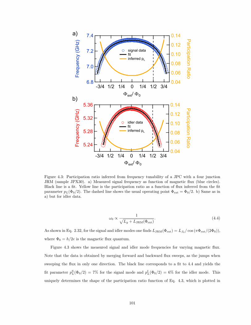
0.14
0.12
0.10
0.08
0.06
0.04
Participation R
atio
-3/4 1/2 1/4 0 1/4 1/2 3/4
7.4
7.2
7.0
6.8Fr
eque
ncy
(GH
z)
signal data fit inferred pL
0.14
0.12
0.10
0.08
0.06
0.04
Participation R
atio
-3/4 1/2 1/4 0 1/4 1/2 3/4
5.36
5.32
5.28
5.24Freq
uenc
y (G
Hz)
idler data fit inferred pL
Φext/ Φ0
Φext/ Φ0
a)
b)
Figure 4.3: Participation ratio inferred from frequency tunability of a JPC with a four junctionJRM (sample JPX30). a) Measured signal frequency as function of magnetic flux (blue circles).Black line is a fit. Yellow line is the participation ratio as a function of flux inferred from the fitparameter pL(Φ0/2). The dashed line shows the usual operating point Φext = Φ0/2. b) Same as ina) but for idler data.
ω0 ∝1√
Lg + LJRM(Φext). (4.4)
As shown in Eq. 2.32, for the signal and idler modes one finds LJRM(Φext) = LJ0/ cos (πΦext/(2Φ0)),
where Φ0 = h/2e is the magnetic flux quantum.
Figure 4.3 shows the measured signal and idler mode frequencies for varying magnetic flux.
Note that the data is obtained by merging forward and backward flux sweeps, as the jumps when
sweeping the flux in only one direction. The black line corresponds to a fit to 4.4 and yields the
fit parameter pSL(Φ0/2) = 7% for the signal mode and pIL(Φ0/2) = 6% for the idler mode. This
uniquely determines the shape of the participation ratio function of Eq. 4.3, which is plotted in
101
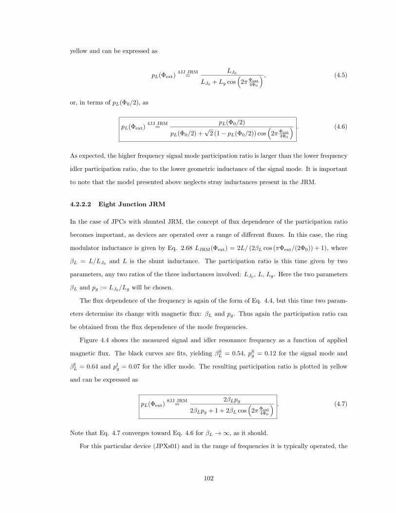
yellow and can be expressed as
pL(Φext)4JJ JRM
=LJ0
LJ0+ Lg cos
(2πΦext
4Φ0
) , (4.5)
or, in terms of pL(Φ0/2), as
pL(Φext)4JJ JRM
=pL(Φ0/2)
pL(Φ0/2) +√
2 (1− pL(Φ0/2)) cos(
2πΦext4Φ0
) . (4.6)
As expected, the higher frequency signal mode participation ratio is larger than the lower frequency
idler participation ratio, due to the lower geometric inductance of the signal mode. It is important
to note that the model presented above neglects stray inductances present in the JRM.
4.2.2.2 Eight Junction JRM
In the case of JPCs with shunted JRM, the concept of flux dependence of the participation ratio
becomes important, as devices are operated over a range of different fluxes. In this case, the ring
modulator inductance is given by Eq. 2.68 LJRM(Φext) = 2L/ (2βL cos (πΦext/(2Φ0)) + 1), where
βL = L/LJ0and L is the shunt inductance. The participation ratio is this time given by two
parameters, any two ratios of the three inductances involved: LJ0, L, Lg. Here the two parameters
βL and pg := LJ0/Lg will be chosen.
The flux dependence of the frequency is again of the form of Eq. 4.4, but this time two param-
eters determine its change with magnetic flux: βL and pg. Thus again the participation ratio can
be obtained from the flux dependence of the mode frequencies.
Figure 4.4 shows the measured signal and idler resonance frequency as a function of applied
magnetic flux. The black curves are fits, yielding βSL = 0.54, pSg = 0.12 for the signal mode and
βIL = 0.64 and pIg = 0.07 for the idler mode. The resulting participation ratio is plotted in yellow
and can be expressed as
pL(Φext)8JJ JRM
=2βLpg
2βLpg + 1 + 2βL cos(
2πΦext4Φ0
) . (4.7)
Note that Eq. 4.7 converges toward Eq. 4.6 for βL →∞, as it should.
For this particular device (JPXs01) and in the range of frequencies it is typically operated, the
102

5.4
5.2
5.0
4.8
4.6
Freq
uenc
y (G
Hz)
-1.5 -1 -0.5 0 0.5 1 1.5
0.20
0.16
0.12
0.08
0.04
Participation R
atio
idler data fit inferred pL
7.8
7.6
7.4
7.2
7.0Freq
uenc
y (G
Hz)
-1.5 -1 -0.5 0 0.5 1 1.5Φext/ Φ0
0.20
0.16
0.12
0.08
0.04
Participation R
atio
signal data fit inferred pL
Φext/ Φ0
a)
b)
Figure 4.4: Participation ratio inferred from frequency tunability of a JPC with shunted JRM(sample JPXs01). a) Measured signal frequency as function of magnetic flux (blue circles). Blackline is a fit. Yellow line is the participation ratio as a function of flux inferred from the fit parametersβL and LJ0/Lg. b) Same as in a) but for idler data.
103

30
20
10
0G
ain
(dB
)
-24 -22 -20 -18 -16 -14
Pump Power (dBm, at generator)
data theory
Figure 4.5: Measured gain vs. applied pump power (blue circles, sample JPXs01) and theoreticalprediction (black).
participation ratio of the signal mode thus varies by a factor of two, between around 7% and 15%
while the idler mode varies between around 5% and 12%.
4.3 Gain Scaling with Pump Power
As explained in Ch. 3 (Eq. 3.15), the JPC scales with the injected pump power Pp as
√G0 =
1 + αPp1− αPp
, (4.8)
where α is a proportionality constant representing the losses between generator and the sample. At
the critical pump power Pp = Ppo, determined by |ρ0|2 = 1, where |ρ0|2 = αPp is the normalized
pump power, the gain is expected to diverge. In reality however, the gain remains finite and levels
off more smoothly than expected by Eq. 4.8, as seen in Fig. 4.5. The data was taken in a resolution
bandwidth (RBW) of 5Hz at a center frequency of 7.64GHz, an care was taken to reduce the probe
tone power used to measure the gain as the gain increased, to assure the device was not saturating
at any point. Two possible explanations for the flattening of the gain compared to the theoretical
black curve (calculated from the experimental gain point at 11 dB), are that the pump impedance
starts changing at higher gains, leading to a deviation from the simple proportionality |ρ0|2 = αPp,
and/or that the device reaches gains which are sufficiently large to excite higher order nonlinearities
in the signal mode with zero-point fluctuations alone. In the case where higher order non-linearities
are excited, the equations of motion Eqs. 3.5 are not valid anymore and no analytical expression
104
20
15
10
5
0
Gai
n (d
B)
8.148.128.108.088.068.048.02Frequency (GHz)
Pump frequency (GHz)14.443 14.49314.453 14.50314.463 14.51314.473 14.52314.483 14.533
Figure 4.6: Measured gain curves for varying pump frequencies (sample JPX14).
of the gain dependence as a function of the pump power can be derived. One would need to use
numerical methods to fit the curve of Fig. 4.5, which was beyond the scope of this work.
4.4 Tunability with Pump Frequency
The pump frequency ωp is the second available parameter of the pump. As shown in Ch. 3 (Eq.
3.6), the center frequency of amplification depends on the exact value of the pump frequency:
G[ω] =
∣∣∣∣∣A?[ω]B?[ωp − ω] + |ρ0|2
A[ω]B?[ωp − ω]− |ρ0|2
∣∣∣∣∣2
, (4.9)
where
A[ω] = 1− iω − ωaγa/2
(4.10)
B[ω] = 1− iω − ωbγb/2
, (4.11)
and ωa,b and γa,b are the signal/idler mode resonant frequencies and linear bandwidths.
Figure 4.6 shows this tunability with pump frequency, which in practice is of the order of γa,b
for the signal/idler mode. The arrows on top indicate the locations of the theoretically expected
105
center frequencies of the gain curves as described by Eq. 4.9. The linear bandwidth for this device
is about 100 MHz and it is frequency tunable with the pump frequency over about 50 MHz. Note
however that the curves represent approximately the maximum gains achieved at the shown tuning
points, and that those maximum gains significantly decrease at the extrema of the tuning. The
narrow range of tunability together with the decrease in gain away from the ideal tuning point
ωp = ωc = ωa + ωb make tunable JPC based on shunted JRMs necessary for practical operation.
4.5 Saturation Powers for Tunable JPC
For JPCs with JRMs without shunt only one working point is in practice considered (Φ = Φ0/2),
so that only one set of parameters determine its saturation behavior. In the tunable JPCs however,
it was found that saturation powers can significantly change depending on the flux point and
pump parameters chosen. Figure 4.7 shows the measured P-1 dB saturation powers as a function
of the gain, for amplifier frequencies tuned from 7.38 GHz to 7.8 GHz. The P-1 dB are defined as
the signal input powers at which the amplifier gain drops by 1 dB, and are extracted from data
similar to the one presented in Fig. 1.9. As becomes apparent, the saturation powers decrease with
increasing gain, with a slope of about −1.2 dB/dB. More importantly, the saturation powers differ
starkly between tuning points, by up to 20 dB. Thus, when tuned to a gain of 20 dB at the center
frequency of 7.8 GHz the device could handle about 10 photons from a qubit readout cavity with
5 MHz (black dotted line represents one photon at 5 MHz). But when tuned to the same gain at a
center frequency of 7.4 GHz it could handle only a fraction of a photon. While this feature is partly
due to the changing participation ratio and coupling strength g3 at different bias points (see Ch. 2
and Sec. 4.2.2), differences of up to 10 dB were observed at close-by tuning points and frequencies,
making it necessary to carefully set frequency bias points using both the flux and pump frequency
tuning. This is likely due to the fact that there is a range of pump frequencies for each flux bias
point at which amplification is possible, but which are not necessarily optimal, in the sense that
the pump frequency is detuned away from the sum of the linear signal and idler frequencies (at
the given flux bias). This question of saturation powers and mechanisms as a function of flux and
pump settings needs to be studied in more detail in the future.
106

-140
-120
-100
P -1
dB (d
Bm
)
2422201816141210Gain (dB)
7.79 GHz 7.70 GHz 7.60 GHz 7.54 GHz 7.50 GHz 7.38 GHz
1 Photon @ 5 MHz
Figure 4.7: Measured P-1 dB input signal saturation powers, at which the gain drops by 1 dB, asfunction of the gain and at different frequency points of a tunable JPC (sample JPXs01).
107

Chapter 5
Coherent Attenuation and Reverse
Operation of the JPC
Three-wave mixing has been known since the early days of nonlinear optics to be a phase sensitive
three wave process, depending on the phase ϕn = ϕS + ϕI − ϕp relevant to this nonlinear system,
where ϕS,I,p are the signal, idler, and pump phases respectively [79], and provides a basic building
block for measurements at the single photon level [80, 81]. Usually the Josephson Parametric
Converter (JPC) is operated as a phase preserving amplifier, and only tones on the signal port
are applied. As explained in Ch. 3, the JPC can also be operated in phase sensitive mode, when
applying tones with equal photon fluxes on both the signal and idler ports. Depending on the
phase ϕn, this can either lead to coherent amplification or its time-reversed equivalent, Coherent
Attenuation (CA), analogous to time-reversal in lasers [82, 83] and optical parametric oscillators
(OPO) [84]. Moreover, power conservation predicts that CA leads to an increase of the circulating
pump amplitude, effectively leading to an increase of the gain of the JPC.
Both effects, the attenuation of signal and idler tones at the CA condition and the increase of
pump photons as manifested through an increase of the gain, will be explored below [67], confirming
that the JPC Hamiltonian must not only have a mixing term of the form a†b†c but also the hermitian
conjugate term abc†.
108

5.1 Theory
5.1.1 Coherent Attenuation
The absorption of balanced signal and idler input tones for small tone amplitudes (stiff pump
approximation still applies) can be fully described by the JPC scattering matrix of Eq. 3.49. For
classical signal and idler wave amplitudes αin = |αin| e−iϕS and βin = |βin| e−iϕI the scattering
matrix becomes:
αout
β?out
=
cosh(λ) −ie−iϕP sinh(λ)
ieiϕP sinh(λ) cosh(λ)
αin
β?in
, (5.1)
where ϕP is the pump phase and√G0 ≡ cosh(λ). Balancing the input photon fluxes |αin|2 ≡ nS
!=
nI ≡ |βin|2 one obtains
αout = cosh(λ) |αin| e−iϕS − ie−iϕP sinh(λ) |βin| e+iϕI (5.2)
= |αin|(cosh(λ)e−iϕS − ie−iϕp sinh(λ)e+iϕI
). (5.3)
The CA |αout|2 / |αin|2 (or ’return loss’ in microwave terminology) on the signal port then is
|αout|2
|αin|2=
∣∣cosh(λ)e−iϕS − ie−iϕp sinh(λ)e+iϕI∣∣2 (5.4)
= cosh2(λ) + sinh2(λ) + i cosh(λ) sinh(λ)(e−i(ϕS+ϕI−ϕp) − e+i(ϕS+ϕI−ϕp)
)(5.5)
= cosh(2λ) + sinh(2λ) cos(ϕS + ϕI − ϕp − π/2) (5.6)
= cosh(2λ)
(cos2(
ϕS + ϕI − ϕp − π/22
) + sin2(ϕS + ϕI − ϕp − π/2
2)
)(5.7)
+ sinh(2λ)
(cos2(
ϕS + ϕI − ϕp − π/22
)− sin2(ϕS + ϕI − ϕp − π/2
2)
)(5.8)
so that finally one arrives at the CA equation :
|αout|2
|αin|2=|βout|2
|βin|2= e2λ cos2
(ϕn − π/2
2
)+ e−2λ sin2
(ϕn − π/2
2
), (5.9)
109

where ϕn := ϕS + ϕI − ϕp is the relevant phase of the three waves1. Thus at large G0, one will
observe a power gain of e2λ ≈ 4G0 at ϕn = +π/2 or CA of e−2λ ≈ 1/(4G0) at ϕn = −π/2, with a
periodicity of 2π.
The same result is of course obtained when considering the (amplitude) eigenvalues e±λ ≈(2√G0
)±1, and corresponding eigenvectors ~e± =(α, αei(ϕP±π/2)
)Tof the scattering matrix of Eq.
5.9. These eigenvalues correspond to ϕn = ±π/2, as expected form Eq. 5.9 and represent injecting
tones α in the signal port and α?e−i(ϕP±π/2) in the idler port.
5.1.2 Gain Modulation
When increasing the signal and idler tone amplitudes (keeping them balanced) eventually the stiff
pump approximation will break down and one has to consider the full nonlinear dynamics of all
three modes (signal, idler, and pump) as predicted by Eq. 3.5. In this case the gain G0 loses its
meaning as power reflection coefficient, but can be interpreted as system state parameter in case
the pump parameters stay untouched throughout the experiment, as is the case here. The return
loss on the signal (and idler) port will then depend on the system state parameter G0 (which still
is the power gain at small injected tones) as well as on the signal and idler photon fluxes relative to
the pump photon flux, captured by the parameter x := nS/nP = (ωc/ωa) · (PS/Pp), where PS(Pp)
is the injected signal (pump) tone power. The resulting signal port power reflection coefficient
G in the fully nonlinear regime is calculated2 by the coupled equations (see supplemental material
of [67])
ρ = ρ0
∣∣∣∣1 + x · ρ0
4
1√G
[(1 +√G)2
e−i(ϕn+π/2) − 2(
1 +√G)√
G− 1 + (G− 1) ei(ϕn+π/2)
]∣∣∣∣ ,(5.10)
and√G =
1 + ρ2
1− ρ2, (5.11)
where
ρ20 ≡√G0 − 1√G0 + 1
. (5.12)
Equations 5.10, 5.11 can be solved numerically but to gain some qualitative insight, one can1This nonlinear phase can of course be redefined by adding a constant offset.2The theory was worked out by A. Roy.
110

expand Eq. 5.10 in terms of 1/√G:
ρ = ρ0
∣∣∣∣1− x · ρ0
2
[2(√
G+ 1)
cos2
(ϕn − π/2
2
)− 1
2√G
(5.13)
+i
(1 +
1√G
)(cos2
(ϕn2
)− sin2
(ϕn2
))]+O
(1
G
)∣∣∣∣ (5.14)
= ρ0
∣∣∣1−x · ρ0
(√G+ 1
)+O
(1√G
)∣∣∣ , for ϕn = +π/2∣∣∣1+x · ρ0
4√G
+O(
1G
)∣∣∣ , for ϕn = −π/2. (5.15)
Equations 5.11, 5.12 show that G is a monotonous function of ρ, so that the minus sign in Eq. 5.15
means that the gain is reduced for ϕn = +π/2, while it is enhanced for ϕn = −π/2 (plus sign),
since for large JPC gains, G0, G 1, ρ0, ρ ≈ 1, and further it can be assumed that x 1. When
ϕn is +π/2, Eq. 5.9 predicts that the JPC (i.e. the pump) has to provide a maximum amount of
power for the amplification process, which for large signal and idler tones becomes unsustainable
and leads to a reduction of the gain G as predicted by Eq. 5.15. At the phase ϕn = −π/2 on
the other hand, signal and idler tones are coherently absorbed (they are suppressed by the factor
e−2λ, Eq. 5.9) and for large signal and idler amplitudes the power reappears as extra pump power,
leading to an enhancement of the JPC gain, as shown by Eq. 5.15.
5.2 Some Experimental Details and JPC Characteristics
The JPC used in this experiment3 is tuned to have a signal center frequency fS = 7.6393 GHz, an
idler center frequency fI = 5.2277GHz with an applied pump tone fp = fS + fI = 12.867 GHz. To
observe the CA at low applied signal and idler powers of Eq. 5.9 as well as the modulation of the gain
at large signal and idler powers as described by Eqs. 5.10, 5.11 the phase ϕn = ϕS +ϕI −ϕp needs
to be varied. To achieve this, the signal and pump phases (ϕS, ϕP) are being kept constant while
the idler phase ϕI is varied in time at a rate of one cycle per 10 seconds, thus very slow compared
to any other time scale in the experiment. This is equivalent to offsetting the idler tone by δf = 0.1
Hz (ϕI(t) = ϕI(0) + φ(t), φ(t) := 2πδf · t) which is what has been done experimentally. Further,
since ϕn is defined only up to a constant, one can choose to set ϕn0:= ϕS +ϕI(0)−ϕp
!= −π/2, so
that ϕn = ϕn0+ φ(t) = −π/2 + φ(t) and Eq. 5.9 yields
3Sample JPXs01, with an inductively shunted Josephson Ring Modulator (JRM).
111
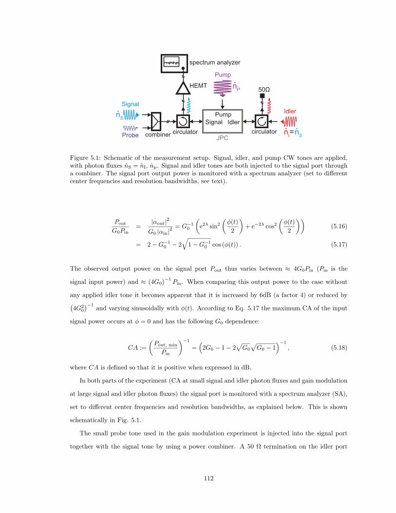
circulator
HEMT
spectrum analyzer
50Ω
circulatorcombiner JPC
IdlerSignal
Probe
Pump
nS
nP
nI= nS Signal Idler
Pump
Figure 5.1: Schematic of the measurement setup. Signal, idler, and pump CW tones are applied,with photon fluxes nS = nI, np. Signal and idler tones are both injected to the signal port througha combiner. The signal port output power is monitored with a spectrum analyzer (set to differentcenter frequencies and resolution bandwidths, see text).
PoutG0Pin
=|αout|2
G0 |αin|2= G−1
0
(e2λ sin2
(φ(t)
2
)+ e−2λ cos2
(φ(t)
2
))(5.16)
= 2−G−10 − 2
√1−G−1
0 cos (φ(t)) . (5.17)
The observed output power on the signal port Pout thus varies between ≈ 4G0Pin (Pin is the
signal input power) and ≈ (4G0)−1Pin. When comparing this output power to the case without
any applied idler tone it becomes apparent that it is increased by 6dB (a factor 4) or reduced by(4G2
0
)−1 and varying sinusoidally with φ(t). According to Eq. 5.17 the maximum CA of the input
signal power occurs at φ = 0 and has the following G0 dependence:
CA :=
(Pout, min
Pin
)−1
=(
2G0 − 1− 2√G0
√G0 − 1
)−1
, (5.18)
where CA is defined so that it is positive when expressed in dB.
In both parts of the experiment (CA at small signal and idler photon fluxes and gain modulation
at large signal and idler photon fluxes) the signal port is monitored with a spectrum analyzer (SA),
set to different center frequencies and resolution bandwidths, as explained below. This is shown
schematically in Fig. 5.1.
The small probe tone used in the gain modulation experiment is injected into the signal port
together with the signal tone by using a power combiner. A 50 Ω termination on the idler port
112

0 f (GHz)
Idler SignalProbe
Pump
∆f = f - ωa/2π(ωa/2π=7.6393GHz)
Signal
Probeδf = 0.1 Hz100 kHz
>1.5 MHz
0
7.64 12.87 5.23
Idler(Up-Converted)
Figure 5.2: Schematic of frequencies involved in the experiment. Top: Signal (blue) and idler(red) amplification bandwidths are shown as Lorentzian shapes. Applied signal and idler tones (redand blue arrows) as well as the probe tone (dark blue arrow) are applied well within amplificationbandwidth. The pump (purple arrow) is at the sum frequency of signal and idler resonators.Bottom: While the signal tone (blue arrow) is applied exactly at the center of amplification, theidler tone (dashed red arrow) is offset by δf = 0.1 Hz, and appearing in the signal resonator throughup-conversion. The offset δf achieves a rolling of the phase ϕn. When applied, the small probetone is offset by 100 kHz from the amplification center.
assures that no amplified outgoing idler port power gets reflected back into the JPC. As mentioned
above, signal and idler input photon fluxes are balanced nS = nI for all experiments described in
this chapter. This is achieved by setting the JPC to very high gains of about 25 dB where the
ratio between G and G − 1 is about 0.01 dB. A small idler tone is then injected in the idler port
and detected at the signal port (after frequency conversion through the JPC and with gain G− 1)
and compared to a small signal tone injected and detected at the signal port. When both tones
are balanced, the resulting amplified tones on the signal port are within 0.01 dB of each other.
After balancing signal and idler inputs this way at the beginning of each experiment, the balance
is frequently checked in the course of the experiment, and typically found to be better than ~0.05
dB (i.e. ~1%).
Figure 5.2 shows the location of signal, probe, idler, and pump tones in frequency space. The
signal tone (blue arrow) is applied at the center of the amplification band (represented by the blue
Lorentzian gain response function), while the idler tone (red arrow) is offset by the idler port center
of amplification (red Lorentzian) by δf = 0.1 Hz to achieve the slow variation of the phase ϕn.
The probe tone is offset from the signal tone by 100 kHz, to assure that the signal tone output
power or the probe tone output power can independently be measured. Figure 5.2 b) further shows
that the idler tone is up-converted in frequency and appears as output power on the signal port
113

25
20
15
10
5
07.667.657.647.637.62
Frequency (GHz)
Fit coefficients:f0 = 7.6393 GHzG0 = 24.8 dBBW = 1.5 MHz
Data Lorentzian fit
Gai
n (d
B)
a) b)25
20
15
10
5
0
Ban
dwid
th (M
Hz)
302520151050
Gain (dB)
Calculated Data point from a)
Figure 5.3: JPC amplification bandwidths in the experiment. a) Measured gain curve (red circles)at G0 ≈ 25 dB. The bandwidth at this gain point is 1.5MHz, as shown by the Lorentzian fit (blackline). b) Predicted bandwidths of the JPC at different gains G0 using the data point in a).
(dashed red arrow), as could be observed with a SA when setting the resolution bandwidth (RBW)
appropriately.
To assure that all tones are well within the JPC amplification bandwidth, gain versus frequency
curves were taken. Figure 5.3 a) shows such a gain curve for G0 ≈ 25 dB and 3 dB-bandwidth of
1.5 MHz, together with a Lorentzian fit. None of the gain settings G0 in these experiments exceed
25 dB, so that the 1.5 MHz represents a lower bound on the JPC bandwidth, since the bandwidth
as a function of gain varies as described by Eq. 3.17.
The calculated 3 dB-bandwidth vs. gain behavior based on this equation and the gain curve
in a) can be seen in Fig. 5.3 b). This observation is important, as it means that all relevant
bandwidths and frequency offsets in the experiments are far smaller than the JPC bandwidth. All
tones can be assumed to be applied at the center of the amplification band and the exact shape of
the gain response function can be neglected.
5.3 Coherent Attenuation
To observe the phase dependence of the JPC as predicted by Eq. 5.17, care must be taken to assure
the JPC operates in the stiff pump approximation. The signal and idler photon fluxes nS = nI (or
in powers PS = ωSωIPI) need to be sufficiently small for every setting of G0 to avoid saturation of the
device. To confirm this, saturation curves were taken, where the signal input power PS was varied
and the signal port gain was measured for pump settings corresponding to different unsaturated
114
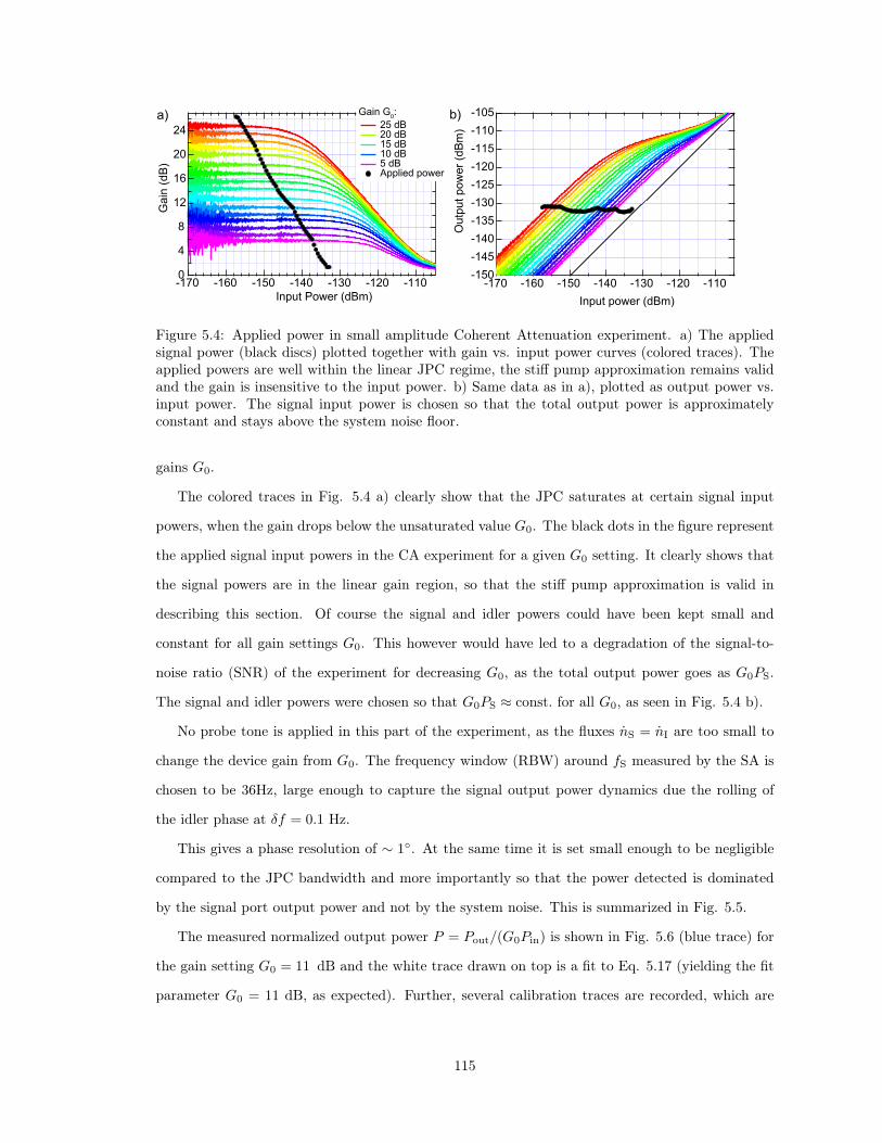
24
20
16
12
8
4
0
Gai
n (d
B)
-170 -160 -150 -140 -130 -120 -110Input Power (dBm)
Gain G0: 25 dB 20 dB 15 dB 10 dB 5 dB Applied power
a)
-150-145-140-135-130-125-120-115-110-105
Out
put p
ower
(dB
m)
-170 -160 -150 -140 -130 -120 -110Input power (dBm)
b)
Figure 5.4: Applied power in small amplitude Coherent Attenuation experiment. a) The appliedsignal power (black discs) plotted together with gain vs. input power curves (colored traces). Theapplied powers are well within the linear JPC regime, the stiff pump approximation remains validand the gain is insensitive to the input power. b) Same data as in a), plotted as output power vs.input power. The signal input power is chosen so that the total output power is approximatelyconstant and stays above the system noise floor.
gains G0.
The colored traces in Fig. 5.4 a) clearly show that the JPC saturates at certain signal input
powers, when the gain drops below the unsaturated value G0. The black dots in the figure represent
the applied signal input powers in the CA experiment for a given G0 setting. It clearly shows that
the signal powers are in the linear gain region, so that the stiff pump approximation is valid in
describing this section. Of course the signal and idler powers could have been kept small and
constant for all gain settings G0. This however would have led to a degradation of the signal-to-
noise ratio (SNR) of the experiment for decreasing G0, as the total output power goes as G0PS.
The signal and idler powers were chosen so that G0PS ≈ const. for all G0, as seen in Fig. 5.4 b).
No probe tone is applied in this part of the experiment, as the fluxes nS = nI are too small to
change the device gain from G0. The frequency window (RBW) around fS measured by the SA is
chosen to be 36Hz, large enough to capture the signal output power dynamics due the rolling of
the idler phase at δf = 0.1 Hz.
This gives a phase resolution of ∼ 1. At the same time it is set small enough to be negligible
compared to the JPC bandwidth and more importantly so that the power detected is dominated
by the signal port output power and not by the system noise. This is summarized in Fig. 5.5.
The measured normalized output power P = Pout/(G0Pin) is shown in Fig. 5.6 (blue trace) for
the gain setting G0 = 11 dB and the white trace drawn on top is a fit to Eq. 5.17 (yielding the fit
parameter G0 = 11 dB, as expected). Further, several calibration traces are recorded, which are
115

spectrum analyzer
∆f = f - ωa/2π(ωa/2π=7.6393GHz)
Signal
δf = 0.1 Hz
0Idler(Up-Converted)
RBW = 36 Hz
JPC BW > 1.5 MHz
Figure 5.5: Schematic of frequency window measured by the spectrum analyzer in the small ampli-tude Coherent Attenuation experiment. The window is centered at the signal tone frequency andits width is set to 36 Hz, leading to a ∼ 1 phase resolution (since δf = 0.1 Hz) in the change of themeasured power. The signal tone power as a function of phase φ is measured for different values ofJPC gain G0.
used to determine the gain G0 and the maximum attenuation CA at φ = 2πn, n ∈ Z.
The pink trace is measured when the idler tone is turned off entirely, so that Pout = G0Pin
(where Pin is the injected signal power). The purple trace is measured with pump and idler tones
turned off, so that Pout = Pin. The black trace shows the system noise floor (pump on; signal and
idler tones off), which for large gains is dominated by the amplified JPC noise. CA is the fraction
of input power that the JPC ’absorbs’ at its maximum CA point φ = 2πn, and thus a measure of
how efficient the device is in converting signal and idler photons into pump photons.
Figure 5.7 shows the normalized output power P = Pout/(G0Pin) for varying gain G0. Clearly
visible is how the maxima approach 6 dB for increasing G0, while the minima tend to −∞.
Plotting the CA (as defined graphically in Fig. 5.6) vs. G0 (blue dots) in Fig. 5.8 shows that
there is good agreement between the experimental result and theory given by Eq. 5.18 (red trace)
up to a gain of about 14 dB.
At larger gains the distance of the received power at φ = 2πn to the noise floor decreases,
and eventually the minimum CA is not measurable anymore, as the power detected by the SA is
dominated entirely by noise. There are two reasons for this effect: first the noise floor moves up
at larger gains as G0, since the JPC gain at some point dominates the system noise; second the
received power at φ = 2πn decreases as (4G0)−1. The black triangles in Fig. 5.8 are the measured
distance to the noise floor, decreasing with larger gain until eventually crossing the red CA trace,
at which point CA cannot be measured anymore. Note that the error bars on the measured (blue)
116
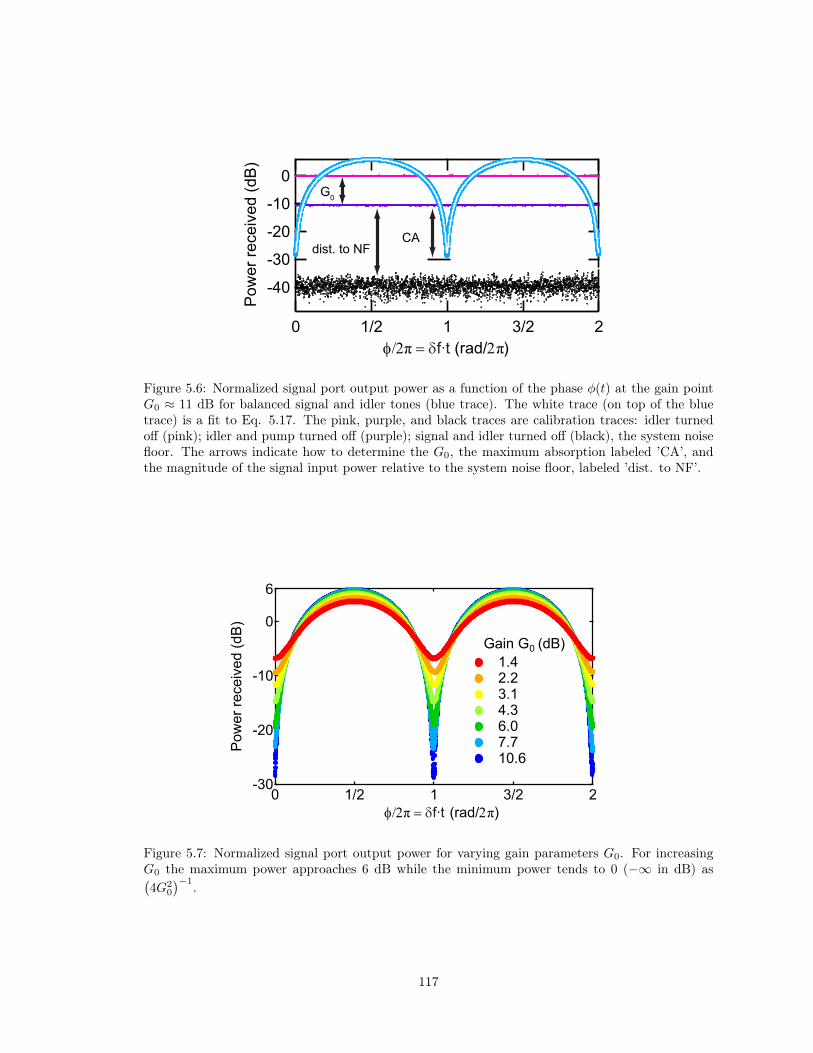
-40
-30
-20
-10
0
Pow
er
receiv
ed (
dB
)
0 1/2 1 3/2 2
(rad/2φ/2ヾ = δf∙t ヾ)
G0
CAdist. to NF
Figure 5.6: Normalized signal port output power as a function of the phase φ(t) at the gain pointG0 ≈ 11 dB for balanced signal and idler tones (blue trace). The white trace (on top of the bluetrace) is a fit to Eq. 5.17. The pink, purple, and black traces are calibration traces: idler turnedoff (pink); idler and pump turned off (purple); signal and idler turned off (black), the system noisefloor. The arrows indicate how to determine the G0, the maximum absorption labeled ’CA’, andthe magnitude of the signal input power relative to the system noise floor, labeled ’dist. to NF’.
-30
-20
-10
0
6
Pow
er
receiv
ed (
dB
)
0 1/2 1 3/2 2
Gain G0 (dB)
1.4 2.2 3.1 4.3 6.0 7.7 10.6
(rad/2φ/2ヾ = δf∙t ヾ)
Figure 5.7: Normalized signal port output power for varying gain parameters G0. For increasingG0 the maximum power approaches 6 dB while the minimum power tends to 0 (−∞ in dB) as(4G2
0
)−1.
117

40
30
20
10
0C
oher
ent A
ttenu
atio
n (d
B)
14121086420Gain (dB)
dist. to NF
Figure 5.8: Coherent Attenuation at maximum interference point vs. gain setting G0 (blue dots).The red curve shows the predicted behavior as described by Eq. 5.18. The black triangles representthe resolution limitation due to the finite distance of the input signal power to the noise floor.
CA points as well as on the ’dist. to noise floor’ data (black) are calculated from the noise floor
data using the Dicke radiometer formula [85], which states that the ’noise on the noise’ power scales
as the noise power itself (with coefficient 1/√Bτ, where B is the bandwidth and τ the integration
time). The error bars on the CA data increase with increasing JPC gain, which is somewhat counter
intuitive. The reason for this is that the output power is kept constant for all G0, as shown in Fig.
5.4 b), while the system noise increases with G0 (the amplified JPC noise increases).
5.4 Gain Enhancement
To prove that at φ = 2πn signal and idler powers are not simply absorbed (i.e. converted to
uncontrolled modes) but converted into pump photons, the gain of the small probe tone injected
into the signal port is monitored. Signal and idler powers are increased to levels that individually
would saturate the JPC and would cause a significant drop in the device gain, as shown in Fig. 5.9.
At the CA point φ = 2πn however, the large signal and idler powers actually lead to an increase
in gain, as signal and idler photons are pairwise annihilated and converted into pump photons. This
increase in circulating pump current leads to an increase in ρ and thus an increase in JPC gain G.
Figure 5.10 shows the frequencies and offsets involved: the SA center frequency is set to the
probe tone frequency with the RBW set to 51 Hz. The probe tone is offset by 100 kHz from the
signal tone, which assures that no signal tone power is detected by the SA. The idler tone is still
offset by δf = 0.1 Hz from the idler center frequency, causing the phase φ to roll at 2π/10sec and
118
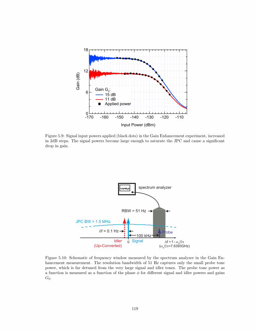
18
12
6
0
Gai
n (d
B)
-170 -160 -150 -140 -130 -120 -110
Input Power (dBm)
Gain G0: 15 dB 11 dB Applied power
Figure 5.9: Signal input powers applied (black dots) in the Gain Enhancement experiment, increasedin 2dB steps. The signal powers become large enough to saturate the JPC and cause a significantdrop in gain.
spectrum analyzer
∆f = f - ωa/2π(ωa/2π=7.6393GHz)
Signal
Probeδf = 0.1 Hz100 kHz
0Idler(Up-Converted)
RBW = 51 Hz
JPC BW > 1.5 MHz
Figure 5.10: Schematic of frequency window measured by the spectrum analyzer in the Gain En-hancement measurement. The resolution bandwidth of 51 Hz captures only the small probe tonepower, which is far detuned from the very large signal and idler tones. The probe tone power asa function is measured as a function of the phase φ for different signal and idler powers and gainsG0.
119

-5-4-3-2-10
Gai
n M
odul
atio
n (d
B)
1440126010809007205403601800Phase (degrees)
a)
180
160
140
120
100
80
60
40
Pha
se (d
egre
es)
160012008004000Trace number (~1min/trace number)
180
160
140
120
100
80
60
40
Phase (degrees)
403020100Countb)
Figure 5.11: G0 set to 11 dB. a) Single trace showing the change of the probe tone gain as a functionof (uncalibrated) phase φ for a particular set of signal and idler powers (trace number 1000). Signaland idler tones are turned on and balanced (nS = nI) for three cycles and turned off for one cyclefor calibration (determining the 0 dB level). b) Left: Tracking of the (uncalibrated) phase φ overthe course of the experiment ( 24 h). For every signal (and idler) power setting, 100 traces similarto the one shown in a) are recorded and subsequently averaged. Right: Histogram of the phase.
leading to a change in JPC gain at a rate of 0.1 Hz.
At fixed G0, the probe power as a function of φ(t) = 2πδf · t is measured for 16 different signal
and idler power settings (again, nS = nI). Signal and idler powers are increased in steps of 2 dB. For
each signal and idler power setting 100 traces of 4 cycles (40 sec) are collected (for later averaging),
where signal and idler tones are turned on for 3 cycles and turned off for one cycle, as shown in Fig.
5.11 a). In this way slow drifts in the JPC gain can be calibrated out. Together with data transfer,
trigger delays and further calibration traces to assure that signal and idler powers are balanced and
the gain G0 does not drift significantly, each trace acquisition takes about 1min, so that the entire
experiment for one gain setting G0 takes about 24 h.
The generator phases drift relative to each other over the course of the experiment, as seen in
Fig. 5.11 b), where the location of the maxima of the individual traces is tracked. The decrease
in noise is simply due to the fact that at small signal and idler power settings very little gain
120

-5
-4
-3
-2
-1
0
Gain
Modula
tion (
dB
)
0 1/2 1 3/2 2
x=nS/n
P
increasing
a)
(rad/2φ/2ヾ = δf∙t ヾ)
-9-8-7-6-5-4-3-2-10
Gain
Modula
tion (
dB
)
0 1/2 1 3/2 2 (rad/2φ/2ヾ = δf∙t ヾ)
x=nS/n
P
increasing
b)
-0.3-0.2-0.10.00.10.20.3
Gai
n M
odul
atio
n (d
B)
7/8 15/16 1 17/16 9/8
c)
(rad/2φ/2π = δf∙t π)
Figure 5.12: Measured (colored traces) probe gain vs. φ for different values of signal and idlerpowers. Signal and idler powers are increased (from blue to red traces) in 2 dB steps. Dashedtraces are numerical least square fits to Eq. 5.10. a) Unsaturated gain set to G0 = 11 dB. b)G0 = 15 dB. c) Enlargement of region around φ = 2π, for G0 = 11 dB. Clearly visible is theincrease of the gain above G0 (0 dB line).
modulation occurs (the individual traces as in a) are flat) and it is more difficult to extract the
location of the maxima. This phase drift is taken into account when averaging the 100 individual
traces together at each signal and idler power setting.
Figure 5.12 shows the resulting (averaged) observed modulation of the gain as a function of the
phase φ(t) for G0 = 11 dB (Fig. 5.12 a) and c)) and G0 = 15 dB (Fig. 5.12 b)). For increasing
signal and idler powers (from blue to red traces) the gain drops significantly at φ = (2n+ 1)π, since
at these locations the maximum output power is extracted from the JPC (as seen in Fig. 5.6 in the
stiff pump case, where Pout ≈ 4G0Pin). This leads to a significant depletion of the pump photons
and a drop of ρ (and thus G), as predicted by Eq. 5.10. The dashed lines are fits to Eqs. 5.10
and 5.11, that correctly reproduce the 2 dB steps in x (or signal and idler powers). The fits start
to deviate around φ = (2n+ 1)π from the experimental curves at large x, which is probably partly
due the larger relative contribution of the system noise floor, as the detected probe power becomes
very small. Further, imbalances in the signal and idler tones will have a more significant effect at
high signal and idler powers. More spectacular however is the observed increase in gain around
121

0.3
0.2
0.1
0.0
Gai
n E
nhan
cem
ent (
dB)
0.150.100.050.00
Expt G0=11 dB Expt G0=15 dB Thy G0=11 dB Thy G0=15 dB
x = nS/nP
Figure 5.13: Gain Enhancement at φ = 2π for G0 = 11 dB (blue) and G0 = 15 dB (red) forincreasing signal-to-pump photon flux ratio x. The circles show the measured values, while thelines are calculated with Eq. 5.10. Experimentally gain enhancement is clearly observed, eventhough only about 1/3 of what is theoretically predicted. Nonetheless the observation of gainenhancement is experimental proof of the reverse parametric operation and ultimately the trilinearnature of the JPC Hamiltonian. See text for possible explanations of the discrepancy betweentheory and experiment.
φ = 2πn, as shown in Fig. 5.12 c). While the drop in gain can easily be achieved with one input
tone (as in Fig. 5.9) and reflects the JPC saturation, the gain enhancement is a distinctly coherent
effect, depending on the presence of both signal and idler tones that need to be balanced and need
to be set to have a particular phase relation with the pump (expressed by the phase ϕn).
Figure 5.13 shows the maximum gain enhancement for G0 = 11 dB and G0 = 15 dB as a
function of x. The solid lines are the calculated values using Eqs. 5.10 and 5.11, the dots are the
data points extracted from the data shown in Figs. 5.12 a) and b). Several experimental factors
can lead to the discrepancy between observed and predicted values, that all lead to diminishing the
observed gain enhancement: since the phase modulation at 0.1 Hz is rather slow, the experiment is
sensitive to 1/f-noise, as well as to the generator phases (Fig. 5.11 b)). Any mismatch between nS
and nI will also significantly lower the gain enhancement. Beyond that, spurious dissipation into
uncontrolled modes in this reverse amplification process will also contribute, so that the results of
Fig. 5.13 can be understood as benchmarks (or lower bounds) on how much control one has over
the signal, idler, and pump modes in JPCs.
122

Chapter 6
Experimental Methods
6.1 Sample Fabrication
The Josephson Parametric Converter (JPC) samples in this work were all fabricated on silicon using
electron beam (e-beam) lithography. Initially (samples JPX01 through JPX20), 2 inch wafers with
high resistivity of at least 9 kΩ×cm and 300 µm thickness were used. To increase the reproducibility
of the resonator characteristics, these were substituted by double-sided polished 3 inch silicon wafers
with resisitivities of at least 1 kΩ×cm and 250 µm thickness (samples JPX22 through JPX30 and
JPXs01 through JPXs04). The second polished side is necessary to deposit a 1.2 µm layer of silver on
the back side of the sample, thus ensuring that the distance of the ground plane to the transmission
line is given solely by the wafer thickness. The silver-backed samples were then glued to the sample
box with silver paste (SPI Supplies Silver Paste Plus) and left to dry at room temperature, while
the first generation of devices on the 300µm thick silicon were usually glued with poly methyl
methacrylate (PMMA) or GE varnish (Lake Shore VGE-7031 varnish) . GE varnish is know to
have good thermal conductivity at low temperatures and is often used to adhere sample chips to
the sample boxes, but has the disadvantage for the microstrip design used here that in practice it
is difficult to reproducibly have only a negligibly thin layer of it. It is easier to achieve thin layers
with PMMA, but it also dries very quickly, so that sometimes only part of the sample area would
be attached to the holder. This can lead to the sample detaching from the holder after thermal
cycling.
All samples measured were fabricated in a single lithography and evaporation step, so that a
123

device JPX09 JPX14 JPX16 JPX22 JPX26 JPX30 JPXs01 JPXs04fab date 100210 100910 101110 110301 110511 110928 110928 120118
Resonator Properties:lengthS/I(mm) 6.5/8.5 6.3/8.5 6.3/9 6.12/9 5.8/9 5.8/9 5.8/9 5.9/8.35gapS/I(µm) 13/13 12/14 12/13 12/13 12/13 6/6 12/13 12/3
substrate t (µm) 300 µm 300 µm 300 µm 250 µm 250 µm 250 µm 250 µm 250 µmTL type w/ holes w/ holes w/ holes solid solid solid solid solid
litho. system NPGS NPGS NPGS NPGS NPGS EBPG EBPG EBPGAg backed no no no X X X X X
JRM X X X X X X
shunted JRM X (Dolan) X (BFT)Junction Properties:
JRM JJ (µm2) 5× 1 5× 1 5× 1 5× 1 5× 1 5× 1 1.5× 1 1.5× 1.5
shunt JJ (µm2) n/a n/a n/a n/a n/a n/a 5× 1 2.3× 2.3
P (Torr) × t (min) 10× 5 10× 5 10× 5 10× 5 10× 5 10× 5 10× 5 10× 5
Ox cleaning X X X X X no no X
Rafter lift-offn (Ω) 80 80 55 60 65 60 - -Iinferred0 (µA) 3.5 3.5 5.1 4.7 4.3 4.7 - -LinferredJ0
(pH) 93 93 64 70 76 70 - -
Table 6.1: List of notable JPC samples with relevant fabrication parameters.
maximum of flexibility was achieved in the choice of sample parameters from one sample to the
next. Aluminum was deposited for all samples in a Plassys MEB550S e-beam evaporator. The
wafers were spun with dual layers of e-beam resist (∼ 90 nm of PMMA on top of ∼ 700 nm of
PMMA), so that a resist undercut could be created and double angle evaporation techniques for
the junction fabrication could be used.
All samples had microstrip resonators of 300 µm width, leading to characteristic impedances
of the transmission lines of 45 Ω (300 µm thick silicon) or 41 Ω (250 µm thick silicon). Typically,
resonators were around 6 mm (signal) and 9 mm (idler) long. Table 6.1 summarizes fabrication pa-
rameters of notable JPC samples measured throughout this thesis work. See Table 4.1 for measured
amplifier parameters of these samples.
6.1.1 E-beam Lithography with Converted SEM
The e-beam lithography for samples JPX01 through JPX29 was done using a converted scanning
electron microscope (SEM) (FEI type 6634/17 30kV) using the NPGS (Nanometer Pattern Gen-
eration System) software. All these devices had (unshunted) Josephson Ring Modulators (JRMs)
with four junctions, all fabricated using the Dolan bridge technique [62]. Two layers of aluminum
of thickness 35 nm and 120 nm were deposited at angles ±40, with an oxidation step in between.
124

Microstrip
Feedline
Coupling Capacitor
JRM
JJ
Figure 6.1: Typical JPC sample with designed holes in transmission line resonators (sample shownis JPX14). Top left: JRM with four junctions. Top right: Single Josephson junction. Bottom left:Gap capacitor for coupling to the 50 Ω environment.
6.1.1.1 Transmission Line Resonator with Holes
The first generation of samples (JPX01 through JPX21) were designed to have microstrip trans-
mission line resonators with irregular holes, to avoid magnetic flux creep during operation. It was
later realized that this precaution was unnecessary (though not harmful) and solid microstrip lines
were fabricated (JPX22 through JPX30 and JPXs01 through JPXs04).
Figure6.1 shows an optical image of a full JPC device, with two insets showing SEM images of
the JRM (top left) and a single junction (top right). The bottom left inset shows a magnification
of the coupling capacitor. The junctions of all (unshunted) JRM fabricated with the Dolan bridge
technique were of 5× 1 µm2.
6.1.1.2 Resist Mask
Figure 6.2 shows SEM images of resist masks created after the e-beam lithography step. Two
features that need to be pointed out are the thin (260 nm wide) bridge that is completely suspended
(no methyl methacrylate (MMA) underneath) and the undercuts above and below the junction
trenches. Note also that the resist edges are not completely straight in the sample shown. This is
not very important for junctions but can be adjusted by increasing the trench doses. The difficulty
then is to make sure that the resistance bridge does not collapse either after the development step
125
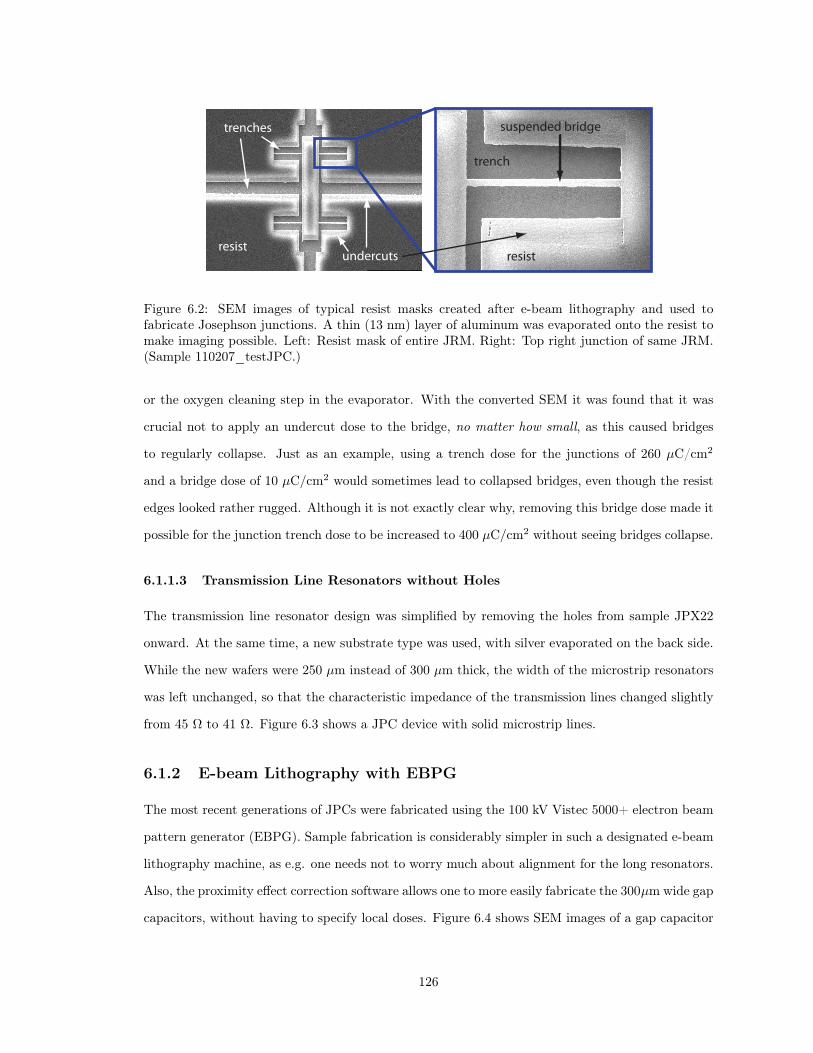
suspended bridge
undercuts
trenches
trench
resistresist
Figure 6.2: SEM images of typical resist masks created after e-beam lithography and used tofabricate Josephson junctions. A thin (13 nm) layer of aluminum was evaporated onto the resist tomake imaging possible. Left: Resist mask of entire JRM. Right: Top right junction of same JRM.(Sample 110207_testJPC.)
or the oxygen cleaning step in the evaporator. With the converted SEM it was found that it was
crucial not to apply an undercut dose to the bridge, no matter how small, as this caused bridges
to regularly collapse. Just as an example, using a trench dose for the junctions of 260 µC/cm2
and a bridge dose of 10 µC/cm2 would sometimes lead to collapsed bridges, even though the resist
edges looked rather rugged. Although it is not exactly clear why, removing this bridge dose made it
possible for the junction trench dose to be increased to 400 µC/cm2 without seeing bridges collapse.
6.1.1.3 Transmission Line Resonators without Holes
The transmission line resonator design was simplified by removing the holes from sample JPX22
onward. At the same time, a new substrate type was used, with silver evaporated on the back side.
While the new wafers were 250 µm instead of 300 µm thick, the width of the microstrip resonators
was left unchanged, so that the characteristic impedance of the transmission lines changed slightly
from 45 Ω to 41 Ω. Figure 6.3 shows a JPC device with solid microstrip lines.
6.1.2 E-beam Lithography with EBPG
The most recent generations of JPCs were fabricated using the 100 kV Vistec 5000+ electron beam
pattern generator (EBPG). Sample fabrication is considerably simpler in such a designated e-beam
lithography machine, as e.g. one needs not to worry much about alignment for the long resonators.
Also, the proximity effect correction software allows one to more easily fabricate the 300µm wide gap
capacitors, without having to specify local doses. Figure 6.4 shows SEM images of a gap capacitor
126

300 µm
12 µm
300 µm
5 µm
Figure 6.3: Optical images of a JPC with solid microstrip lines. The top pictures show the devicecenter, with the a magnification of the JRM on the right. The bottom pictures show the bottomgap capacitor, connecting the feed line to the transmission line resonator. (Sample JPX22.)
resist mask and a gap capacitor of a JPC test device. The mask was imaged after sputtering a thin
layer (∼ 10 nm) of gold. The gap capacitors are 5 µm and 3 µm wide over a length of 300 µm and
were chosen here to demonstrate that the EBPG proximity correction software is quite good for
these devices (gap sizes at or below 5 µm become difficult to fabricate with the converted SEM).
Three versions of JRMs were fabricated using the EBPG: Four junction rings very similar to the
ones shown above; Shunted JRMs with junctions using the Dolan bridge technique; And shunted
JRMs using the bridge-free technique.
5 µm
substrate
resist 3 µm substrate
aluminuma) b)
Figure 6.4: SEM and optical images of two samples: a) test chip with gap capacitor resist maskand b) JPC gap capacitor using the EBPG. (Samples 110816_captest and 111107_shuntedJPC.)
127

a) b)
Figure 6.5: SEM images of junction resist mask (a), tilted by 40 and junction (b) fabricated withthe EBPG. (Samples 110812_RMD and 110824_testJPC.)
6.1.2.1 JRM with Four Dolan Junctions
Figure 6.5 a) shows a SEM image of a junction resist mask, fabricated using the EBPG. The mask
is shown at an angle of 40, making it apparent that the bridge is suspended and that no resist
remains underneath the undercuts. Figure 6.5 b) shows a Josephson junction fabricated with the
EBPG. The dark areas are believed to be (insulating) aluminum oxide folding back onto the leads
from the resist walls during lift-off.
6.1.2.2 Shunted JRM with Eight Dolan Junctions
Figure 6.6 shows a test device with eight Josephson junctions fabricated using the Dolan bridge
technique. The large shunt junctions have a size of 5 × 1 µm2 and the small junctions have an
area of 1.5 × 1 µm2. The one device successfully measured in the course of this work, which was
fabricated with eight Dolan type Josephson junctions is JPXs01.
6.1.2.3 Shunted JRM with Eight BFT Junctions
A simpler way to make large Josephson junctions without having to worry about potentially col-
lapsing bridges is to use the bridge-free technique (BFT) [63]. Instead of using a suspended bridge
to separate the two junction electrodes, only one side of the leads connecting to the junction elec-
trodes has undercuts. This way, arbitrary junction sizes and shapes can in principle be achieved,
but constraints are set on the lead widths and lengths. Figure 6.7 shows a) a schematic of the mask
design and b) an SEM image of the resulting Josephson junction. As can be seen, only one side
of each junction lead receives an undercut dose (blue). When evaporating aluminum at two angles
128
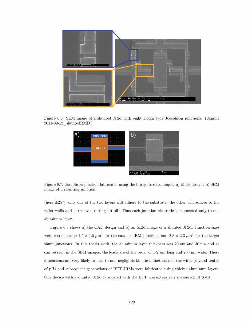
Figure 6.6: SEM image of a shunted JRM with eight Dolan type Josephson junctions. (Sample2011-09-12_shuntedRMD.)
trench
undercuta) b)
Figure 6.7: Josephson junction fabricated using the bridge-free technique. a) Mask design. b) SEMimage of a resulting junction.
(here ±25), only one of the two layers will adhere to the substrate, the other will adhere to the
resist walls and is removed during lift-off. Thus each junction electrode is connected only to one
aluminum layer.
Figure 6.8 shows a) the CAD design and b) an SEM image of a shunted JRM. Junction sizes
were chosen to be 1.5 × 1.5 µm2 for the smaller JRM junctions and 2.3 × 2.3 µm2 for the larger
shunt junctions. In this thesis work, the aluminum layer thickness was 20 nm and 30 nm and as
can be seen in the SEM images, the leads are of the order of 1-2 µm long and 200 nm wide. These
dimensions are very likely to lead to non-negligible kinetic inductances of the wires (several tenths
of pH) and subsequent generations of BFT JRMs were fabricated using thicker aluminum layers.
One device with a shunted JRM fabricated with the BFT was extensively measured: JPXs04.
129

a) b)
Figure 6.8: Shunted JRM fabricated using the bridge-free technique. a) CAD mask design. b) SEMimage of a shunted JRM. (Sample 120114_BridgeFreeJRM)
6.1.3 Junction Aging
JPC samples were typically cooled down within a few days of sample fabrication. In this time, the
large 5× 1µm2 junctions fabricated with the Dolan bridge technique aged on average by ∼ 2 Ω per
day when cleaned with an argon-oxygen plasma before the deposition of the first aluminum layer.
Typical resistance values (depending on the oxidation parameters) were from 50-100 Ω. Aging
would vary significantly from wafer to wafer when removing the plasma cleaning step (e.g. to
avoid collapsing bridges), and this although all wafers were cleaned with the same procedure before
spinning resist. A “dirty” wafer could let the junctions age by as much as 300% within 24 hours of
lift-off. Figure 6.9 shows the change of junction resistance vs. time for the junctions of a typical test
JRM fabricated with the converted SEM. An optical microscope image of the measured device is
shown on the right, which underwent plasma cleaning before the evaporation. The reference value
of the junction resistance measured right after lift-off was 73 Ω and the change refers to this initial
value. In the first week after lift-off, the rate of change is approximately constant (∼ 2 Ω per day),
and levels off afterward.
6.2 Sample Holder
JPC samples were mounted onto a copper sample holder base, initially using PMMA or GE varnish
(Lake Shore VGE-7031 varnish), and most recently silver paste (SPI Supplies Silver Paste Plus).
The advantage of silver paste is that it provides good thermal conductivity to samples with thin
layers (1 − 2µm) of silver evaporated on the substrate back side, while at the same time tying
130

40
30
20
10
0
Junc
tion
resi
stan
ce c
hang
e in
%
160012008004000
Hours after lift-off
706050403020100
Days after lift-off
Figure 6.9: Change in measured Josephson junction resistance measured after lift-off. The testdevice is shown on the right. (Sample 100728_RMD.)
Figure 6.10: Photos of sample holder. From left to right: Sample holder base with mounted JPCsample, to be connected to two hybrids. Base with mounted JPC sample, to be connected to onehybrid (signal resonator shorted to ground on one side). Sample holder lid. Closed sample holderwith Anritsu connectors (photo courtesy of Anirudh Narla).
together sample and sample holder ground planes. The sample holder lid together with the base
form a cavity with approximate dimensions 1.85 × 1.85 × 0.5 cm3. Anritsu K103F-R microwave
connectors are attached to the holder base, designed with spacings compatible with Krytar hybrid
couplers, so that they can be connected without additional transmission lines. Figure 6.10 shows
JPC samples mounted onto sample holder bases (left two images), the sample holder lid, and the
entire closed sample holder. A magnetic coil is placed in a small recess on the lid back side. Two
types of printed circuit board (Rogers TMM 10I) 50 Ω transmission lines were used: One in a cross
shape (left most image), when connecting both signal and idler resonators to hybrids, and the other
with only one transmission line trace for the signal port (second image). In that case, the second
resonator feed line was wire-bonded to ground.
A groove in the lid allows the box to be sealed with indium wire, ensuring good electrical contact
131

-120-100-80-60-40
Tra
nsm
issi
on (
dB)
20151050
Frequency (GHz)
Figure 6.11: Insertion loss of sample box when connecting two of its ports to the network analyzer.The lowest box mode is above 11 GHz.
between lid and base. This is crucial to make sure no spurious resonant modes appear near the
signal and idler frequencies. The lowest box mode for this geometry is at around 11GHz, as can be
seen in Fig. 6.11. Note that the presence of the sample and PC board pulls this frequency down by
only a few 100MHz, and thus it is still far away from typical signal and idler resonance frequencies
of around 8 GHz and 6 GHz respectively.
6.3 Setup
6.3.1 Heliox Refrigerator
Experiments up to sample JPX09 were performed at around 250 mK in a Oxford Heliox 3He
refrigerator. One JPC sample was measured per cooldown, with a typical line diagram shown in
Fig. 6.12. Signal and Idler input and output were separated by cryogenic circulators. Stainless
steel cables were used between temperature stages inside the inner vacuum can (IVC), ensuring
little thermal conductivity between them. high electron mobility transistor (HEMT) amplifiers on
the output lines, separated by two isolators from the sample, amplified signals reflected off the
device. The JPC samples were placed in high magnetic permeability Permalloy shields (Cryoperm
by Amuneal) to minimize magnetic field noise in the JRM.
6.3.2 Triton Refrigerator
The majority of samples (JPX09-JPX30 and JPXs01-JPXs04) were measured in a cryogen free
dilution refrigerator (Oxford Triton 200) at temperatures of around 25 mK. A typical wiring
diagram of the microwave lines is shown in Fig. 6.13. A six-way switch (Radiall) at base allowed
132

1K
4K
IdlerIN SignalIN Pump
-40 dB (-10-10-10-10)
-30 dB
(-10-10-10)
-40 dB
(-20-20)
-30 dB
(-20-10)
250mK
300K
HEMT Caltech
L014
HEMT Caltech
L033
7-10 GHz
4-12 GHz
Stainless Steel
Thermalization through copper 4-8 GHz
7-10 GHz
4-8 GHz
IdlerOUT SignalOUT
Thermalization in He bath
-30 dB
(-20-10)
Copper
4K
IVC
-33 dB (-3-20-10)
~ -2.5 dB
4-8 GHz
~ -2.5 dB ~ -2.5 dB
~ -2 dB
~ -2.7 dB
~ -1.7 dB
Idler Signal
Pump
JPC
Figure 6.12: Wiring diagram of microwave lines in the Heliox refrigerator. One JPC sample can bemeasured at a time.
one to switch between several JPCs at low temperatures, so that several devices could be measured
in a single cooldown. Also shown is a qubit which could be switched in or out with an additional
transfer switch. Superconducting niobium-titanium cables were used to connect to the HEMT
amplifiers and reduce losses without creating a thermal link between the temperature stages. Input
lines were heavily attenuated to reduce room temperature noise to below quantum fluctuations.
Figure6.14 shows a JPC sample at the refrigerator base temperature stage, symmetrically cou-
pled to two hybrids, using short hand-formable copper cables. Also visible is a closed cryoperm
shielding can on the left.
133

300K
40 K
2.6 K
690 mK
130 mK
25 mK
~ -7.5 dB
1 2 3 4 5 6 7 8
-20 -20 -30 -20 -20 -20 -30
~ -10 dB
P P P Ø I S1 Ø S2 DC block
DC block
DC block
DC block
DC block
DC block
DC block
-10 -10 -3 -20
X-fer switch 6-way
switch
1 2 3 4 5 6
JPC
JPC
JPC
JPC
DC
6-way switch
1 2 3 4 5 6
D C
-3
HEMT LNF #51
HEMT LNF #53
NbTi
~ -0.8 dB
~ - 2.5 dB
DC block
NbTi
~ -0.8 dB
-3
-30 -30 -30 -30 -30 -20 -30 -20
DC
1kΩ
1 2 3 4 5 6 7 8
7-10 GHz
8-12 GHz
4-12 GHz 4-12 GHz
4-12 GHz
4-8 GHz
5 8 6
D C
D C Sig. Idl.
~ - 2 dB
7-10 GHz
Figure 6.13: Wiring diagram of microwave lines in the Triton refrigerator. Six-way switches at thebase stage allow for several samples to be measured during the same cooldown
Figure 6.14: JPC sample mounted on dilution refrigerator base stage. Two cryoperm shields arevisible, one open to access the sample. The right copper plate is a mount for the three microwaveswitches.
134

Chapter 7
Conclusion & Outlook
This thesis summarizes my work on building and operating a practical, quantum-limited, phase-
preserving superconducting microwave parametric amplifier (paramp), the Josephson Parametric
Converter (JPC), with the goal of making it useful for the readout of superconducting quantum bits
(qubits). First, a new design of the JPC was developed, making the device parameters predictable
and reproducible. The simple device fabrication, with only one lithography and evaporation step,
considerably simplified device development, allowing to easily change all relevant parameters from
one device to the next. The addition of a silver layer on the substrate back plane assured the
reproducibility of resonator frequencies within a few MHz between nominally identical devices and
thermal cycling.
Second, devices with parameters matching those of qubit readout cavities were developed. These
JPCs had frequencies of between 5 and 8 GHz, amplifier bandwidths of 3 to 10 MHz at gains of
20 dB, while capable of processing a few photons and adding no more than 5/2 photons of noise,
close to the quantum limit of 1/2. This allowed to improve the measurement efficiency in the
measurement of a transmon qubit to 0.2− 0.4, which is sufficiently close to the ideal value of 1 to
perform variable strength measurements while observing the backaction, and to monitor the qubit
state in real-time.
Third, the addition of shunt inductors in the Josephson Ring Modulator (JRM) made the new
generation of JPCs frequency tunable, lifting the last major hurdle in using the JPC for qubit
readout. Precise frequency matching of better than 5 MHz is required, the typical qubit readout
cavity and JPC amplification bandwidths, and the tunable JPCs now easily achieve a tunability of
135
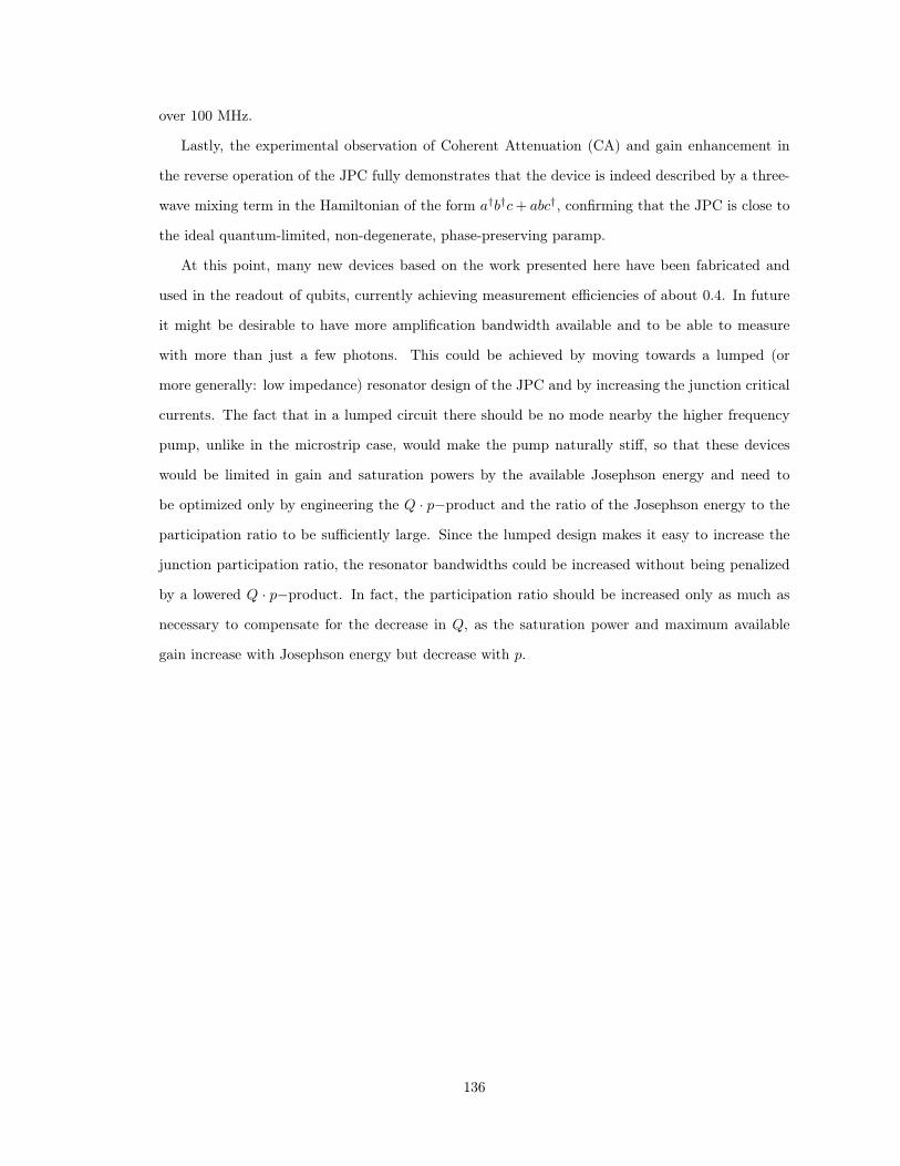
over 100 MHz.
Lastly, the experimental observation of Coherent Attenuation (CA) and gain enhancement in
the reverse operation of the JPC fully demonstrates that the device is indeed described by a three-
wave mixing term in the Hamiltonian of the form a†b†c+ abc†, confirming that the JPC is close to
the ideal quantum-limited, non-degenerate, phase-preserving paramp.
At this point, many new devices based on the work presented here have been fabricated and
used in the readout of qubits, currently achieving measurement efficiencies of about 0.4. In future
it might be desirable to have more amplification bandwidth available and to be able to measure
with more than just a few photons. This could be achieved by moving towards a lumped (or
more generally: low impedance) resonator design of the JPC and by increasing the junction critical
currents. The fact that in a lumped circuit there should be no mode nearby the higher frequency
pump, unlike in the microstrip case, would make the pump naturally stiff, so that these devices
would be limited in gain and saturation powers by the available Josephson energy and need to
be optimized only by engineering the Q · p−product and the ratio of the Josephson energy to the
participation ratio to be sufficiently large. Since the lumped design makes it easy to increase the
junction participation ratio, the resonator bandwidths could be increased without being penalized
by a lowered Q · p−product. In fact, the participation ratio should be increased only as much as
necessary to compensate for the decrease in Q, as the saturation power and maximum available
gain increase with Josephson energy but decrease with p.
136
Bibliography
[1] H. J. Kimble. Squeezed states of light: An (incomplete) survey of experimental progress and
prospects. Physics Report, 219(3-6):227–234, 1992. Cited By (since 1996): 48. 3
[2] P. A. Franken, A. E. Hill, C. W. Peters, and G. Weinreich. Generation of optical harmonics.
Phys. Rev. Lett., 7:118–119, Aug 1961. 3
[3] W.H. Louisell. Coupled mode and parametric electronics. Wiley, 1960. 3
[4] H. A. Haus and J. A. Mullen. Quantum noise in linear amplifiers. Phys. Rev., 128:2407–2413,
Dec 1962. 3
[5] Carlton M. Caves. Quantum limits on noise in linear amplifiers. Phys. Rev. D, 26:1817–1839,
Oct 1982. 3, 10, 89
[6] A. A. Clerk, M. H. Devoret, S. M. Girvin, Florian Marquardt, and R. J. Schoelkopf. Introduc-
tion to quantum noise, measurement, and amplification. Rev. Mod. Phys., 82:1155–1208, Apr
2010. 3
[7] Chonghoon Kim, Ruo-Ding Li, and Prem Kumar. Deamplification response of a traveling-wave
phase-sensitive optical parametric amplifier. Opt. Lett., 19(2):132–134, Jan 1994. 3
[8] Sang-Kyung Choi, Ruo-Ding Li, Chonghoon Kim, and Prem Kumar. Traveling-wave optical
parametric amplifier: investigation of its phase-sensitive and phase-insensitive gain response.
J. Opt. Soc. Am. B, 14(7):1564–1575, Jul 1997. 3, 6
[9] Joseph Kakande, Carl Lundström, Peter A. Andrekson, Zhi Tong, Magnus Karlsson, Periklis
Petropoulos, Francesca Parmigiani, and David J. Richardson. Detailed characterization of
a fiber-optic parametric amplifier in phase-sensitive and phase-insensitive operation. Opt.
Express, 18(5):4130–4137, Mar 2010. 3, 7
137

[10] Takeshi Umeki, Osamu Tadanaga, Atsushi Takada, and Masaki Asobe. Phase sensitive degen-
erate parametric amplification using directly-bonded PPLN ridge waveguides. Opt. Express,
19(7):6326–6332, Mar 2011. 3
[11] Masaki Asobe, Takeshi Umeki, and Osamu Tadanaga. Phase sensitive amplification with noise
figure below the 3 dB quantum limit using CW pumped PPLN waveguide. Opt. Express,
20(12):13164–13172, Jun 2012. 3, 7
[12] R. E. Slusher, L. W. Hollberg, B. Yurke, J. C. Mertz, and J. F. Valley. Observation of squeezed
states generated by four-wave mixing in an optical cavity. Phys. Rev. Lett., 55:2409–2412, Nov
1985. 3, 4
[13] B. Yurke, P. G. Kaminsky, R. E. Miller, E. A. Whittaker, A. D. Smith, A. H. Silver, and R. W.
Simon. Observation of 4.2-K equilibrium-noise squeezing via a Josephson-parametric amplifier.
Phys. Rev. Lett., 60:764–767, Feb 1988. 4
[14] B. Yurke, L. R. Corruccini, P. G. Kaminsky, L. W. Rupp, A. D. Smith, A. H. Silver, R. W.
Simon, and E. A. Whittaker. Observation of parametric amplification and deamplification in
a Josephson parametric amplifier. Phys. Rev. A, 39:2519–2533, Mar 1989. 4
[15] R. Movshovich, B. Yurke, P. G. Kaminsky, A. D. Smith, A. H. Silver, R. W. Simon, and M. V.
Schneider. Observation of zero-point noise squeezing via a Josephson-parametric amplifier.
Phys. Rev. Lett., 65:1419–1422, Sep 1990. 4
[16] H. Zimmer. Parametric amplification of microwaves in superconducting josephson tunnel junc-
tions. Applied Physics Letters, 10(7):193–195, 1967. 4
[17] N. F. Pedersen, M. R. Samuelsen, and K. Saermark. Parametric excitation of plasma oscilla-
tions in josephson junctions. Journal of Applied Physics, 44(11):5120–5124, 1973. 4
[18] J. Mygind, N. F. Pedersen, O. H. Soerensen, B. Dueholm, and M. T. Levinsen. Low-noise
parametric amplification at 35 GHz in a single Josephson tunnel junction. Applied Physics
Letters, 35(1):91–93, 1979. 4
[19] M. H. Devoret and R. J. Schoelkopf. Superconducting circuits for quantum information: An
outlook. Science, 339(6124):1169–1174, 2013. 4
138
[20] M. A. Castellanos-Beltran and K. W. Lehnert. Widely tunable parametric amplifier based
on a superconducting quantum interference device array resonator. Applied Physics Letters,
91(8):083509, 2007. 4, 9, 74, 81
[21] M. A. Castellanos-Beltran, K. D. Irwin, G. C. Hilton, L. R. Vale, and K. W. Lehnert. Ampli-
fication and squeezing of quantum noise with a tunable Josephson metamaterial. Nat. Phys.,
4(12):928–931, 2008. 4
[22] T. Yamamoto, K. Inomata, M. Watanabe, K. Matsuba, T. Miyazaki, W. D. Oliver, Y. Naka-
mura, and J. S. Tsai. Flux-driven Josephson parametric amplifier. Applied Physics Letters,
93(4):042510, 2008. 4, 10, 74, 81, 86
[23] M. Hatridge, R. Vijay, D. H. Slichter, John Clarke, and I. Siddiqi. Dispersive magnetometry
with a quantum limited SQUID parametric amplifier. Phys. Rev. B, 83:134501, Apr 2011. 4,
9, 74, 81
[24] N. Bergeal, F. Schackert, M. Metcalfe, R. Vijay, V. E. Manucharyan, L. Frunzio, D. E. Prober,
R. J. Schoelkopf, S. M. Girvin, and M. H. Devoret. Phase-preserving amplification near the
quantum limit with a Josephson ring modulator. Nature, 465(7294):64–68, May 2010. 4, 20
[25] N. Bergeal, R. Vijay, V. E. Manucharyan, I. Siddiqi, R. J. Schoelkopf, S. M. Girvin, and M. H.
Devoret. Analog information processing at the quantum limit with a Josephson ring modulator.
Nat. Phys., 6(4):296–302, April 2010. 4, 27, 70
[26] Baleegh Abdo, Flavius Schackert, Michael Hatridge, Chad Rigetti, and Michel Devoret. Joseph-
son amplifier for qubit readout. Applied Physics Letters, 99(16):162506, 2011. 4, 28, 31
[27] Baleegh Abdo, Archana Kamal, and Michel Devoret. Nondegenerate three-wave mixing with
the Josephson ring modulator. Phys. Rev. B, 87:014508, Jan 2013. 4, 27, 28, 30, 69, 70, 75
[28] N. Roch, E. Flurin, F. Nguyen, P. Morfin, P. Campagne-Ibarcq, M. H. Devoret, and B. Huard.
Widely tunable, nondegenerate three-wave mixing microwave device operating near the quan-
tum limit. Phys. Rev. Lett., 108:147701, Apr 2012. 4, 25, 26, 31, 64
[29] Erik A. Tholén, Adem Ergül, Evelyn M. Doherty, Frank M. Weber, Fabien Grégis, and David B.
Haviland. Nonlinearities and parametric amplification in superconducting coplanar waveguide
resonators. Applied Physics Letters, 90(25):253509, 2007. 4, 74, 81
139

[30] B. Ho Eom, P. K. Day, H. G. Leduc, and J. Zmuidzinas. A wideband, low-noise superconducting
amplifier with high dynamic range. Nat. Phys., 8(8):623–627, 2012. Cited By (since 1996): 5.
4, 7
[31] M. Mück and R. McDermott. Radio-frequency amplifiers based on dc SQUIDs. Superconductor
Science and Technology, 23(9), 2010. Cited By (since 1996): 10. 4
[32] Lafe Spietz, Kent Irwin, and José Aumentado. Input impedance and gain of a gigahertz
amplifier using a dc superconducting quantum interference device in a quarter wave resonator.
Applied Physics Letters, 93(8):082506, 2008. 4
[33] Lafe Spietz, Kent Irwin, and José Aumentado. Superconducting quantum interference device
amplifiers with over 27 Ghz of gain-bandwidth product operated in the 4–8 Ghz frequency
range. Applied Physics Letters, 95(9):092505, 2009. 4
[34] Lafe Spietz, Kent Irwin, Minhyea Lee, and José Aumentado. Noise performance of lumped
element direct current superconducting quantum interference device amplifiers in the 4–8 Ghz
range. Applied Physics Letters, 97(14):142502, 2010. 4
[35] Archana Kamal, John Clarke, and Michel H. Devoret. Gain, directionality, and noise in mi-
crowave SQUID amplifiers: Input-output approach. Phys. Rev. B, 86:144510, Oct 2012. 4
[36] J. D. Teufel, T. Donner, M. A. Castellanos-Beltran, J. W. Harlow, and K. W. Lehnert. Nanome-
chanical motion measured with an imprecision below that at the standard quantum limit.
Nature Nanotechnology, 4(12):820–823, 2009. Cited By (since 1996):107. 4
[37] R. Vijay, D. H. Slichter, and I. Siddiqi. Observation of quantum jumps in a superconducting
artificial atom. Phys. Rev. Lett., 106:110502, Mar 2011. 5, 12, 17, 33
[38] D. Ristè, C. C. Bultink, K. W. Lehnert, and L. DiCarlo. Feedback control of a solid-state qubit
using high-fidelity projective measurement. Phys. Rev. Lett., 109:240502, Dec 2012. 5, 17
[39] D. Ristè, J. G. van Leeuwen, H.-S. Ku, K. W. Lehnert, and L. DiCarlo. Initialization by
measurement of a superconducting quantum bit circuit. Phys. Rev. Lett., 109:050507, Aug
2012. 5
140
[40] R. Vijay, C. MacKlin, D. H. Slichter, S. J. Weber, K. W. Murch, R. Naik, A. N. Korotkov, and
I. Siddiqi. Stabilizing Rabi oscillations in a superconducting qubit using quantum feedback.
Nature, 490(7418):77–80, 2012. Cited By (since 1996): 7. 5, 17
[41] P. Campagne-Ibarcq, E. Flurin, N. Roch, D. Darson, P. Morfin, M. Mirrahimi, M. H. Devoret,
F. Mallet, and B. Huard. Stabilizing the trajectory of a superconducting qubit by projective
measurement feedback. ArXiv e-prints, January 2013. 5, 17
[42] M. Hatridge, S. Shankar, M. Mirrahimi, F. Schackert, K. Geerlings, T. Brecht, K. M. Sliwa,
B. Abdo, L. Frunzio, S. M. Girvin, R. J. Schoelkopf, and M. H. Devoret. Quantum back-action
of an individual variable-strength measurement. Science, 339(6116):178–181, 2013. 5, 17, 33,
35
[43] B. Yurke and E. Buks. Performance of cavity-parametric amplifiers, employing Kerr nonlin-
earites, in the presence of two-photon loss. Journal of Lightwave Technology, 24(12):5054–5066,
2006. Cited By (since 1996):40. 9
[44] I. Siddiqi, R. Vijay, F. Pierre, C. M. Wilson, M. Metcalfe, C. Rigetti, L. Frunzio, and M. H.
Devoret. RF-driven Josephson bifurcation amplifier for quantum measurement. Phys. Rev.
Lett., 93:207002, Nov 2004. 9
[45] Rajamani Vijayaraghavan. Josephson Bifurcation Amplifier: Amplifying quantum signals using
a dynamical bifurcation. PhD thesis, Yale University, 2008. 9
[46] R. Vijay, M. H. Devoret, and I. Siddiqi. Invited review article: The Josephson bifurcation
amplifier. Review of Scientific Instruments, 80(11), 2009. Cited By (since 1996): 43. 9
[47] Archana Kamal, Adam Marblestone, and Michel Devoret. Signal-to-pump back action and
self-oscillation in double-pump Josephson parametric amplifier. Phys. Rev. B, 79:184301, May
2009. 9
[48] J. M. Manley and H.E. Rowe. Some general properties of nonlinear elements-part i. general
energy relations. Proceedings of the IRE, 44(7):904–913, 1956. 14
[49] M. Devoret, S. Girvin, and R. Schoelkopf. Circuit-QED: How strong can the coupling between
a Josephson junction atom and a transmission line resonator be? Annalen der Physik (Leipzig),
16(10-11):767–779, 2007. Cited By (since 1996):61. 16
141

[50] A. Wallraff, D. I. Schuster, A. Blais, L. Frunzio, R. . Huang, J. Majer, S. Kumar, S. M.
Girvin, and R. J. Schoelkopf. Strong coupling of a single photon to a superconducting qubit
using circuit quantum electrodynamics. Nature, 431(7005):162–167, 2004. Cited By (since
1996):1129. 16, 33
[51] D. I. Schuster, A. A. Houck, J. A. Schreier, A. Wallraff, J. M. Gambetta, A. Blais, L. Frunzio,
J. Majer, B. Johnson, M. H. Devoret, S. M. Girvin, and R. J. Schoelkopf. Resolving photon
number states in a superconducting circuit. Nature, 445(7127):515–518, 2007. Cited By (since
1996):257. 16
[52] S. Haroche and J.-M. Raimond. Exploring the Quantum: Atoms, Cavities, and Photons.
Oxford University Press, USA, 2006. 16
[53] S. Gleyzes, S. Kuhr, C. Guerlin, J. Bernu, S. Deléglise, U. Busk Hoff, M. Brune, J. . Raimond,
and S. Haroche. Quantum jumps of light recording the birth and death of a photon in a cavity.
Nature, 446(7133):297–300, 2007. Cited By (since 1996):149. 16
[54] N. Wadefalk, A. Mellberg, I. Angelov, M. E. Barsky, S. Bui, E. Choumas, R. W. Grundbacher,
E. L. Kollberg, R. Lai, N. Rorsman, P. Starski, J. Stenarson, D. C. Streit, and H. Zirath.
Cryogenic wide-band ultra-low-noise IF amplifiers operating at ultra-low DC power. IEEE
Transactions on Microwave Theory and Techniques, 51(6):1705–1711, 2003. Cited By (since
1996):67. 17
[55] Jens Koch, Terri M. Yu, Jay Gambetta, A. A. Houck, D. I. Schuster, J. Majer, Alexandre Blais,
M. H. Devoret, S. M. Girvin, and R. J. Schoelkopf. Charge-insensitive qubit design derived
from the Cooper pair box. Phys. Rev. A, 76:042319, Oct 2007. 17
[56] J. A. Schreier, A. A. Houck, J. Koch, D. I. Schuster, B. R. Johnson, J. M. Chow, J. M.
Gambetta, J. Majer, L. Frunzio, M. H. Devoret, S. M. Girvin, and R. J. Schoelkopf. Suppressing
charge noise decoherence in superconducting charge qubits. Physical Review B - Condensed
Matter and Materials Physics, 77(18), 2008. Cited By (since 1996):126. 17
[57] A. A. Houck, J. Koch, M. H. Devoret, S. M. Girvin, and R. J. Schoelkopf. Life after charge
noise: Recent results with transmon qubits. Quantum Information Processing, 8(2-3):105–115,
2009. Cited By (since 1996):22. 17, 33
142

[58] V. E. Manucharyan, J. Koch, L. I. Glazman, and M. H. Devoret. Fluxonium: Single Cooper-
pair circuit free of charge offsets. Science, 326(5949):113–116, 2009. Cited By (since 1996):57.
17, 33
[59] Hanhee Paik, D. I. Schuster, Lev S. Bishop, G. Kirchmair, G. Catelani, A. P. Sears, B. R.
Johnson, M. J. Reagor, L. Frunzio, L. I. Glazman, S. M. Girvin, M. H. Devoret, and R. J.
Schoelkopf. Observation of high coherence in Josephson junction qubits measured in a three-
dimensional circuit QED architecture. Phys. Rev. Lett., 107:240501, Dec 2011. 17, 33
[60] M. Hatridge et al. In preparation. 2013. 17
[61] D.M. Pozar. Microwave engineering. Wiley, 1997. 18, 97
[62] G. J. Dolan. Offset masks for lift-off photoprocessing. Applied Physics Letters, 31(5):337–339,
1977. 20, 46, 65, 124
[63] F. Lecocq, I. M. Pop, Z. Peng, I. Matei, T. Crozes, T. Fournier, C. Naud, W. Guichard,
and O. Buisson. Junction fabrication by shadow evaporation without a suspended bridge.
Nanotechnology, 22(31), 2011. Cited By (since 1996):3. 20, 65, 128
[64] M. Goppl, A. Fragner, M. Baur, R. Bianchetti, S. Filipp, J. M. Fink, P. J. Leek, G. Puebla,
L. Steffen, and A. Wallraff. Coplanar waveguide resonators for circuit quantum electrodynam-
ics. Journal of Applied Physics, 104(11):113904, 2008. 22
[65] K. Sliwa and M. Hatridge. Private communication. 26
[66] N. Bergeal, F. Schackert, L. Frunzio, D. E. Prober, and M. H. Devoret. Mesoscopic resistor as
a self-calibrating quantum noise source. Applied Physics Letters, 100(20):203507, 2012. 31
[67] Flavius Schackert, Ananda Roy, Michael Hatridge, Michel H. Devoret, and A. Douglas Stone.
Three-wave mixing with three incoming waves: Signal-idler coherent attenuation and gain
enhancement in a parametric amplifier. Phys. Rev. Lett., 111:073903, Aug 2013. 36, 108, 110
[68] E. Flurin. Amplificateur paramétrique Josephson près de la limite quantique. Master’s thesis,
École Normale Supérieure, 2011. 45
[69] B. Abdo, A. Kamal, and M. H. Devoret. Fluctuating Nonlinear Oscillators: From Nanome-
chanics to Quantum Superconducting Circuits. OUP Oxford, 2012. 69
143

[70] N. Bergeal, F. Schackert, L. Frunzio, and M. H. Devoret. Two-mode correlation of microwave
quantum noise generated by parametric down-conversion. Phys. Rev. Lett., 108:123902, Mar
2012. 74, 93, 95
[71] E. Flurin, N. Roch, F. Mallet, M. H. Devoret, and B. Huard. Generating entangled microwave
radiation over two transmission lines. Phys. Rev. Lett., 109:183901, Oct 2012. 74, 93, 95
[72] C. E. Shannon. A mathematical theory of communication. The Bell System Technical Journal,
27:379–423, 623–656, 1948. 75
[73] C. E. Shannon and W. Weaver. The Mathematical Theory of Communication. University of
Illinois Press, 1971. 75
[74] Archana Kamal, John Clarke, and M. H. Devoret. Noiseless non-reciprocity in a parametric
active device. Nat. Phys., 7(4):311–315, Apr 2011. 81
[75] Baleegh Abdo, Katrina Sliwa, Flavius Schackert, Nicolas Bergeal, Michael Hatridge, Luigi
Frunzio, A. Douglas Stone, and Michel Devoret. Full coherent frequency conversion between
two propagating microwave modes. Phys. Rev. Lett., 110:173902, Apr 2013. 85
[76] S. Friberg, C. K. Hong, and L. Mandel. Measurement of time delays in the parametric pro-
duction of photon pairs. Phys. Rev. Lett., 54:2011–2013, May 1985. 93
[77] I. J. Bahl and Ramesh Garg. Simple and accurate formulas for a microstrip with finite strip
thickness. Proceedings of the IEEE, 65(11):1611–1612, 1977. Cited By (since 1996):38. 99
[78] Ramesh Garg and I. J. Bahl. Microstrip discontinuities. International Journal of Electronics,
45(1):81–87, 1978. Cited By (since 1996):22. 99
[79] J. A. Armstrong, N. Bloembergen, J. Ducuing, and P. S. Pershan. Interactions between light
waves in a nonlinear dielectric. Phys. Rev., 127:1918–1939, Sep 1962. 108
[80] Alain Aspect, Philippe Grangier, and Gérard Roger. Experimental tests of realistic local
theories via Bell’s theorem. Phys. Rev. Lett., 47:460–463, Aug 1981. 108
[81] Paul G. Kwiat, Klaus Mattle, Harald Weinfurter, Anton Zeilinger, Alexander V. Sergienko,
and Yanhua Shih. New high-intensity source of polarization-entangled photon pairs. Phys.
Rev. Lett., 75:4337–4341, Dec 1995. 108
144

[82] Y. D. Chong, Li Ge, Hui Cao, and A. D. Stone. Coherent perfect absorbers: Time-reversed
lasers. Phys. Rev. Lett., 105:053901, Jul 2010. 108
[83] Wenjie Wan, Yidong Chong, Li Ge, Heeso Noh, A. Douglas Stone, and Hui Cao. Time-reversed
lasing and interferometric control of absorption. Science, 331(6019):889–892, 2011. 108
[84] Stefano Longhi. Time-reversed optical parametric oscillation. Phys. Rev. Lett., 107:033901,
Jul 2011. 108
[85] R. H. Dicke. The measurement of thermal radiation at microwave frequencies. Review of
Scientific Instruments, 17(7):268–275, 1946. 118
145

Appendix A
Transmission Line Resonators
The purpose of this appendix chapter is to calculate the quality factor of transmission line resonators
capacitively coupled to a 50 Ω environment. As will be shown below, for a fixed resonator frequency
and characteristic transmission line impedance, the quality factor is entirely determined by the
coupling capacitors. This is important as it allows to engineer the Josephson Parametric Converter’s
(JPC) signal and idler linear resonator bandwidths, which in turn determine the amplification
bandwidth of the device.
A.1 Parallel RLC Resonator
In this section, we review the parallel RLC circuit1. It is the basis to all further analysis and will
allow us to easily determine the resonance frequency as well as the quality factor Q of a transmission
line resonator. There are three references we use for all of the following notes: Wallraff’s notes on
SC solid state qubits, Pozar, and chapter 3 of Dave Schuster’s PhD thesis.1See Pozar, 3rd edition, pages 269-272
146

C R
Zlumped ωlumpedc 0
L
Figure A.1: RLC resonant circuit.
The input impedance of a parallel RLC resonant circuit is 2 (see figure A.1):
Zin(ω) =
(1
R+
1
jωL+ jωC
)−1
=
(1
R+
1
jωlumped0 L
( 1
1 + ∆ω/ωlumped0
)+ jωlumped0 C + j∆ωC
)−1
≈(
1
R+
1
jωlumped0 L
(1−∆ω/ωlumped0
)+ jωlumped0 C + j∆ωC
)−1
=
(1
R+
j∆ω
(ωlumped0 )2L+ j∆ωC
)−1
=
(1
R+ 2j∆ωC
)−1
=R
1 + 2j∆ωRC
(A.1)
for ω = ωlumped0 + ∆ω and ∆ω ωlumped0 . We thus find:
Zin ≈R
1 + 2jQ∆ω/ωlumped0
for ω = ωlumped0 + ∆ω (A.2)
and ∆ω ωlumped0
Where we have used the following identities:2See Pozar, page 270, eqn. (6.19)
147

ωlumped0 ≡ 1√LC
(A.3)
Q ≡ ωlumped0 RC =R
Zlumpedc
(A.4)
Zlumpedc ≡√L
C(A.5)
A.2 Transmission Line Resonator
In this section we want to show that an open-circuited λ/2 transmission line (TL) has the same input
impedance as a parallel RLC circuit when ∆ω ω0. The input impedance of an open-circuited
TL of length l is3 (see figure (A.2)):
Z0, vp, α+jβ, l
Zinn
Figure A.2: Open-ended TL.
Zin = Z0 coth(αl + jβl) (A.6)
= Z01 + j tanβl tanhαl
tanhαl + j tanβl, (A.7)
3see Pozar, page 276; Wallraff notes, section 2.2, page 8
148

where α(ω), β(ω), Z0(ω), l(=const.) completely define the transmission line, with
Z0(ω) =
√R+ jωLG + jωC
(A.8)
γ(ω) = α+ jβ =√
(R+ jωL)(G + jωC) (A.9)
vp(ω) =1
β(ω)ω =
λ(ω)
2πω = λ(f)f. (A.10)
Note at this point that in the most general case vp = v(ω) which defines the dispersion re-
lation of the TL. In most cases we encounter, vp =const., as for instance for TEM waves where
vp = c√εr
=const. (assuming εr is not a function of frequency). Also in the lossless case (or low-loss
case, see below) we have vp = 1√LC =const. (unless C or L are frequency dependent through e.g. εr).
We now want to consider only frequencies ω around the harmonics ωn of the TL. The condition
for a TL line of fixed length l to be resonating is that a multiple of half a wavelenth fits into l:
nλn2
= l. (A.11)
This equation defines the wavelengths of the n-th harmonic, which occur at the frequency ωn.
Equation (A.10) then allows us to explicitly calculate the frequencies at which the resonant condition
is met:
ωn = nπvpl
= nω1 (A.12)
and
βl = nπω
ωn= nπ + π
∆ωnω1
, (A.13)
with ∆ωn := ω − ωn.
For frequencies close to resonance, i.e. for ω = ωn + ∆ωn and ∆ωn ω14, and using the
identity tan(nπ + x) = tanx and tanβl ≈ π∆ωnω1
and assuming that the TL has small losses
(tanhαl ≈ αl), we then find the input impedance of the TL around the n-th mode to be:
Znin ≈Z0/n
(α/n)l + jπ∆ωnωn
for ω = ωn + ∆ωn (A.14)
and ∆ωn ω1
4Note that this condition is the same as for the parallel RLC case only for the first mode. For higher modes thiscondition is stricter.
149

A.3 Mapping of an (unloaded) TL Resonator to a RLC Res-
onator
Comparing equation (A.2) to equation (A.14) shows that around the n-th harmonic (ω ≈ ωn), we
can map an (unloaded) TL resonator to a RLC resonator, with the following equalities (see figure
A.3):
Zlumpedc,n =
√LnCn
=2
π
Z0
n(A.15)
ωlumpedn = ωn =1√LnCn
= nω1 (A.16)
Rn =Z0
αl= R1 (A.17)
Cn =π
2ωnZ0/n=
π
2ω1Z0= C1 (A.18)
Ln =2Z0/n
πωn=L1
n2, (A.19)
where Rn, Ln, and Cn are the parameters for the equivalent RLC resonator around ωn.
Zlumped ωlumpedc,n n
Ln Cn Rn
Figure A.3: Parallel RLC resonant circuit equivalent to an open-ended TL (see figure (A.2)) aroundresonance.
Finally the correspondence allows us to determine the quality factor of the unloaded TL res-
onator around the n-th harmonic as
Qn =nπ
2αl= nQ1 (A.20)
150
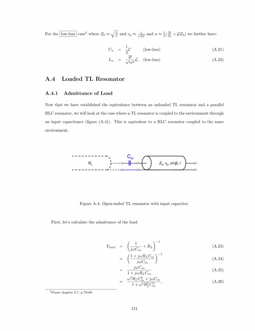
For the low-loss case5 where Z0 ≈√LC and vp ≈ 1√
LC and α ≈ 12 ( RZ0
+ GZ0) we further have:
Cn =l
2C (low-loss) (A.21)
Ln =2l
n2π2L. (low-loss) (A.22)
A.4 Loaded TL Resonator
A.4.1 Admittance of Load
Now that we have established the equivalence between an unloaded TL resonator and a parallel
RLC resonator, we will look at the case where a TL resonator is coupled to the environment through
an input capacitance (figure (A.4)). This is equivalent to a RLC resonator coupled to the same
environment.
Z0, vp, α+jβ, l
CinRL
Figure A.4: Open-ended TL resonator with input capacitor.
First, let’s calculate the admittance of the load:
Yload =
(1
jωCin+RL
)−1
(A.23)
=
(1 + jωRLCin
jωCin
)−1
(A.24)
=jωCin
1 + jωRLCin(A.25)
=ω2RLC
2in + jωCin
1 + ω2R2LC
2in
, (A.26)
5Pozar chapter 2.7, p.79-80
151

where Cin and RL are the input capacitor and the load resistor (or impedance of the measurement
line) respectively. This is equivalent to an effective capacitor C∗ and effective resistor R∗ in parallel,
which has the admittance
Yload
Cin
RL
Cn Rn
Zc,n, ωn
Ln
Figure A.5: A transmission line with impedance RL capacitively coupled to a TL-resonator isequivalent to a loaded RLC resonant circuit. Parallel RLC resonator loaded with an input capacitorand a load resistor.
R*C*
Zc,n, ωn
Ln Cn Rn
Figure A.6: A transmission line with impedance RL capacitively coupled to a TL-resonator isequivalent to a loaded RLC resonant circuit. Equivalent circuit to figure A.5.
Yload = jωC∗ +1
R∗. (A.27)
Comparing equation (A.27) to equation (A.26) allows us to identify:
152

C∗ = Cin1
1 + q2in
(A.28)
R∗ = RL1 + q2
in
q2in
(A.29)
qin := ωRLCin. (A.30)
A.4.2 External Q: Input Coupling Only
As a last step we will now determine the Q of the loaded resonator. For this we can just use the
results from section A.1 a second time with
C = Cn + C∗ ≡ C1 + C∗ (A.31)
R =
((Rn)−1 + (R∗)−1
)−1
≡(
(R1)−1 + (R∗)−1
)−1
(A.32)
L = Ln ≡L1
n2(A.33)
ω0,n =1√LC
= n1√
L1(C1 + C∗)(A.34)
According to equation (A.4) we then have
Q =1
Zc· 1
ReYtotal(A.35)
=
√C
L·R (A.36)
=
√CnLn
√Cn + C∗
Cn·(
1
Rn+
1
R∗
)−1
(A.37)
=
√CnLn
ωnω0,n︸︷︷︸ ·
(1
Rn+
1
R∗
)−1
(A.38)
correction factor
eqn.(A.15)=
nπ
2
1
Z0
ωnω0,n
·(
1
Rn+
1
R∗
)−1
(A.39)
=nπ
2
1
Z0
ω1
ω0,1·(
1
R1+
1
R∗
)−1
(A.40)
eqn.(A.28)=
nπ
2
1
Z0
ω1
ω0,1·(
1
R1+
11
ω2nC
2inRL
+RL
)−1
(A.41)
=
(1
Qint+
1
Qext
)−1
. (A.42)
153

With this definition of Qint we have already taken care of the loading6. For the external quality
factor we thus find:
Qext =1
ZcReYload=
ω1
ω0,1
1
Zc,nReYload(A.43)
Qext =nπ
2
1
Z0
ω1
ω0,1·(
1
n2ω21C
2inRL
+RL
)(A.44)
with
Z0 : Impedance of the resonantTL section (typically 50 Ω)
RL : Impedance of themeasurementTL (typically 50 Ω)
Cin : Input capacitor (what you actuallyDESIGN)
ω0,1 : Fundamental of LOADEDresonator (what youMEASURE)
ω1 : Fundamental of unloaded resonator
n : number of harmonic
A.4.3 External Q: Input and Output Coupling
According to Wallraff’s notes7, having an input and output capacitor Cin and Cout on each side
of the TL resonator (figure (A.7)) corresponds just to having two load circuits, which are effectively
in parallel.
Z0, vp, α+jβ
Cin CoutRL RL
l
Figure A.7: TL resonator with input and output capacitor.
6Alternatively we could defineQint as the quality factor of the bare (unloaded) resonator. ThenQ−1 =ω0,1
ω1Q−1int+
Q−1ext and Qint ≡ Qn.7Section 2.4.1, equation (2.25), page 10. See also Goeppl’s and Wallraff’s 2008 CPW paper.
154

For Cin = Cout we then have to replace C∗ → 2 · C∗ and R∗ → 12 ·R
∗:
Qext =nπ
4
1
Z0
ω1
ω0,1·(
1
n2ω21C
2inRL
+RL
), (A.45)
where now ω1
ω0,1=
√C1+ 2 C∗
C1.
155

Appendix B
Recipes Used for JPC Fabrication
B.1 Spinning Resist
B.1.1 Wafer Cleaning
• 2 minutes ultrasound in NMP
• 2 minutes ultrasound in acetone
• 2 minutes ultrasound in methanol
• blow dry
B.1.2 Spinning
Co-polymer MMA-MAA EL13 (see Fig. B.1):
• 3000 rpm for 90 seconds
• bake at 175 C for 60 seconds
PMMA 950K A4 (see Fig. B.2):
• 4000 rpm for 90 seconds
• bake at 175 C for 30 minutes
156
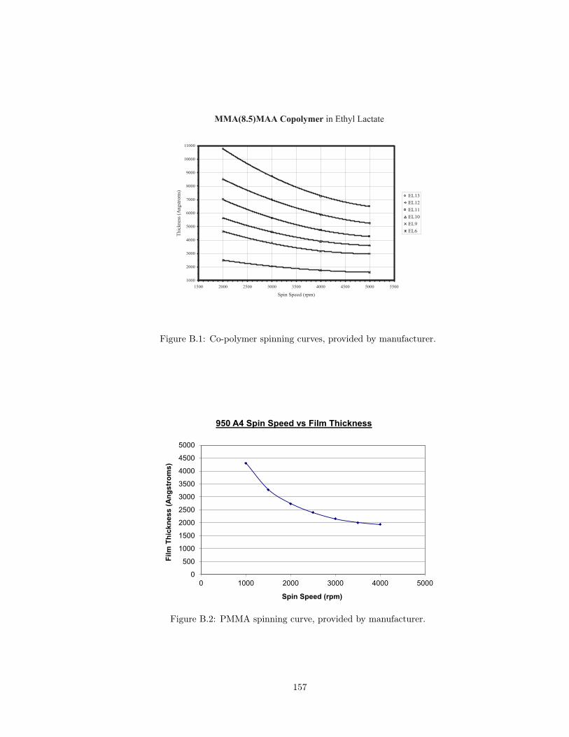
MMA(8.5)MAA Copolymer in Ethyl Lactate
1000
2000
3000
4000
5000
6000
7000
8000
9000
10000
11000
1500 2000 2500 3000 3500 4000 4500 5000 5500
Spin Speed (rpm)
)smortsgn
A( ssenkcihT
EL13EL12EL11EL10EL9EL6
Figure B.1: Co-polymer spinning curves, provided by manufacturer.
0
500
1000
1500
2000
2500
3000
3500
4000
4500
5000
0 1000 2000 3000 4000 5000
Film
Thi
ckne
ss (A
ngst
rom
s)
Spin Speed (rpm)
950 A4 Spin Speed vs Film Thickness
Figure B.2: PMMA spinning curve, provided by manufacturer.
157

B.2 Development
B.2.1 Dolan Bridge Technique
• with tweezers, slowly wave sample in MIBK:IPA solution (3:1) for 50 seconds at 25 C
• remove and dip sample in IPA for 10 seconds, to stop resist development
• blow dry with dry nitrogen
B.2.2 Bridge Free Technique
• submerge sample (with tweezers or preferably with strainer) in IPA:water solution (1:3) for 2
minutes, ultra-sound turned on
• dry off with dry nitrogen
B.3 Aluminum Deposition
All samples were evaporated in the Plassys MEB550S electron beam (e-beam) evaporator.
B.3.1 Dolan Bridge Technique
• oxygen-argon (1sccm:3.5sccm) plasma cleaning: 250 V, 30 seconds
• titanium sweep
• evaporation of first Al layer: 35 nm at rate of 1 nm/s and +40
• oxidation (15% oxygen, 85% argon): at 10 Torr for 5 minutes (typical values)
• evaporation of second Al layer: 120 nm at rate of 1 nm/s and −40
• capping oxidation: at 10 Torr for 5 minutes
• lift-off: place in hot (65 C) acetone for ca. 20 min. Rinse with (cold) acetone and IPA, blow
dry with dry nitrogen
158
B.3.2 Bridge-Free Technique
Same as above with following differences:
• angles are ±25
• Al layer thickness: 20 nm and 30 nm
• lift-off: place in hot (90 C) NMP for ca. 1h. Ulrasound for 20 seconds. Rinse with IPA,
blow dry with dry nitrogen
159