tle4941c in pg-sso-2-4
TRANSCRIPT

March 2010
ATV SC AE
Final Data Sheet Revis ion 3.0
TLE4941C in PG-SSO-2-4Dif ferent ia l Two-Wire Hal l Ef fect Sensor- IC for Wheel Speed Appl icat ions

Edition March 2010Published byInfineon Technologies AG81726 München, Germany© 2010 Infineon Technologies AGAll Rights Reserved.
Legal DisclaimerThe information given in this document shall in no event be regarded as a guarantee of conditions or characteristics. With respect to any examples or hints given herein, any typical values stated herein and/or any information regarding the application of the device, Infineon Technologies hereby disclaims any and all warranties and liabilities of any kind, including without limitation, warranties of non-infringement of intellectual property rights of any third party.
InformationFor further information on technology, delivery terms and conditions and prices, please contact the nearest Infineon Technologies Office (www.infineon.com).
WarningsDue to technical requirements, components may contain dangerous substances. For information on the types in question, please contact the nearest Infineon Technologies Office.
Infineon Technologies components may be used in life-support devices or systems only with the express written approval of Infineon Technologies, if a failure of such components can reasonably be expected to cause the failure of that life-support device or system or to affect the safety or effectiveness of that device or system. Life support devices or systems are intended to be implanted in the human body or to support and/or maintain and sustain and/or protect human life. If they fail, it is reasonable to assume that the health of the user or other persons may be endangered.

Final Data Sheet 3 Revision 3.0, March 2010
TLE4941C
Revision History: March 2010, Revision 3.0Previous Version: September 2007, Data Sheet, V2.2Page Subjects (major changes since last revision)all Changes due to PCN 2009-069-A5 New Ordering Code inserted
We Listen to Your CommentsAny information within this document that you feel is wrong, unclear or missing at all?Your feedback will help us to continuously improve the quality of this document.Please send your proposal (including a reference to this document) to:[email protected]

Final Data Sheet 4 Revision 3.0, March 2010
TLE4941C in PG-SSO-2-4
Table of Contents . . . . . . . . . . . . . . . . . . . . . . . . . . . . . . . . . . . . . . . . . . . . . . . . . . . . . . . . . . . . . . . . 4
1 Product Description . . . . . . . . . . . . . . . . . . . . . . . . . . . . . . . . . . . . . . . . . . . . . . . . . . . . . . . . . . . . . . 51.1 Overview . . . . . . . . . . . . . . . . . . . . . . . . . . . . . . . . . . . . . . . . . . . . . . . . . . . . . . . . . . . . . . . . . . . . . . . . 51.2 Features . . . . . . . . . . . . . . . . . . . . . . . . . . . . . . . . . . . . . . . . . . . . . . . . . . . . . . . . . . . . . . . . . . . . . . . . 5
2 Functional Description . . . . . . . . . . . . . . . . . . . . . . . . . . . . . . . . . . . . . . . . . . . . . . . . . . . . . . . . . . . . 62.1 General . . . . . . . . . . . . . . . . . . . . . . . . . . . . . . . . . . . . . . . . . . . . . . . . . . . . . . . . . . . . . . . . . . . . . . . . . 62.2 Pin Configuration and Marking . . . . . . . . . . . . . . . . . . . . . . . . . . . . . . . . . . . . . . . . . . . . . . . . . . . . . . . 62.3 Block Diagram . . . . . . . . . . . . . . . . . . . . . . . . . . . . . . . . . . . . . . . . . . . . . . . . . . . . . . . . . . . . . . . . . . . 72.3.1 Output Description . . . . . . . . . . . . . . . . . . . . . . . . . . . . . . . . . . . . . . . . . . . . . . . . . . . . . . . . . . . . . . . 8
3 Specification . . . . . . . . . . . . . . . . . . . . . . . . . . . . . . . . . . . . . . . . . . . . . . . . . . . . . . . . . . . . . . . . . . . . 93.1 Absolute Maximum Ratings . . . . . . . . . . . . . . . . . . . . . . . . . . . . . . . . . . . . . . . . . . . . . . . . . . . . . . . . . 93.2 Operating Range . . . . . . . . . . . . . . . . . . . . . . . . . . . . . . . . . . . . . . . . . . . . . . . . . . . . . . . . . . . . . . . . 103.3 Electrical Characteristics . . . . . . . . . . . . . . . . . . . . . . . . . . . . . . . . . . . . . . . . . . . . . . . . . . . . . . . . . . 113.4 Typical Diagrams (measured performance) . . . . . . . . . . . . . . . . . . . . . . . . . . . . . . . . . . . . . . . . . . . . 133.5 Electro Magnetic Compatibility (EMC) . . . . . . . . . . . . . . . . . . . . . . . . . . . . . . . . . . . . . . . . . . . . . . . . 16
4 Package Information . . . . . . . . . . . . . . . . . . . . . . . . . . . . . . . . . . . . . . . . . . . . . . . . . . . . . . . . . . . . 184.1 Package Outline . . . . . . . . . . . . . . . . . . . . . . . . . . . . . . . . . . . . . . . . . . . . . . . . . . . . . . . . . . . . . . . . . 194.2 Packing . . . . . . . . . . . . . . . . . . . . . . . . . . . . . . . . . . . . . . . . . . . . . . . . . . . . . . . . . . . . . . . . . . . . . . . . 19
Table of Contents

Product Name Product Type Ordering Code PackageTLE4941C in PG-SSO-2-4 Diff. Speed Sensor SP000710666 PG-SSO-2-4
PG SSO 2 2
Final Data Sheet 5 Revision 3.0, March 2010
Differential Two-Wire Hall Effect Sensor IC
TLE4941C in PG-SSO-2-4
1 Product Description
1.1 OverviewThe Hall Effect sensor IC TLE4941C is designed to provide informationabout rotational speed to modern vehicle dynamics control systems andABS. The output has been designed as a two wire current interface. Thesensor operates without external components and combines a fast power-up time with a low cut-off frequency. Excellent accuracy and sensitivity isspecified for harsh automotive requirements as a wide temperature range,high ESD and EMC robustness. State-of-the art BiCMOS technology isused for monolithic integration of the active sensor areas and the signalconditioning circuitry.Finally, the optimized piezo compensation and the integrated dynamicoffset compensation enable easy manufacturing and elimination ofmagnet offsets.The TLE4941C is additionally provided with an overmolded 1.8 nFcapacitor for improved EMI performance.
1.2 Features• Two-wire current interface• Dynamic self-calibration principle• Single chip solution• No external components needed• High sensitivity• South and north pole pre-induction possible• High resistance to piezo effects• Large operating air-gaps• Wide operating temperature range• TLE4941C: 1.8 nF overmolded capacitor

Final Data Sheet 6 Revision 3.0, March 2010
TLE4941C in PG-SSO-2-4
Functional Description
2 Functional Description
2.1 GeneralThe differential hall sensor IC detects the motion of ferromagnetic and permanent magnet structures by measuringthe differential flux density of the magnetic field. To detect the motion of ferromagnetic objects the magnetic fieldmust be provided by a back biasing permanent magnet. Either south or north pole of the magnet can be attachedto the rear unmarked side of the IC package.Magnetic offsets of up to ± 20 mT and device offsets are cancelled by a self-calibration algorithm. Only a fewtransitions are necessary for self-calibration. After the initial calibration sequence switching occurs when the inputsignal is crossing the arithmetic mean of its max. and min. value (e.g. zero-crossing for sinusoidal signals).The ON and OFF state of the IC are indicated by High and Low current consumption.
2.2 Pin Configuration and Marking
Figure 1 Pin Description (view on branded side of component)
AEP03200
Center ofsensitive area
CCV GND
21
2.67
2.5
1.44
B B
A
0.3
A0.
3
G: green packageYY: production yearWW: production week
123456:41C0R TLE4941C

Final Data Sheet 7 Revision 3.0, March 2010
TLE4941C in PG-SSO-2-4
Functional Description
2.3 Block Diagram
Figure 2 Block Diagram
The circuit is supplied internally by a 3 V voltage regulator. An on-chip oscillator serves as clock generator for thedigital part of the circuit.TLE4941C signal path is comprised of a pair of hall probes, spaced at 2.5 mm, a differential amplifier including anoise-limiting low-pass filter and a comparator feeding a switched current output stage. In addition an offsetcancellation feedback loop is provided by a signal-tracking A/D converter, a digital signal processor (DSP) and anoffset cancellation D/A converter.During the startup phase (un-calibrated mode) the output is disabled (I = ILOW).The differential input signal is digitized in the speed A/D converter and fed into the DSP. The minimum andmaximum values of the input signal are extracted and their corresponding arithmetic mean value is calculated. Theoffset of this mean value is determined and fed into the offset cancellation DAC. After successful correction of the offset, the output switching is enabled.In running mode (calibrated mode) the offset correction algorithm of the DSP is switched into a low-jitter mode,avoiding oscillation of the offset DAC LSB. Switching occurs at zero-crossing. It is only affected by the (small)remaining offset of the comparator and by the remaining propagation delay time of the signal path, mainlydetermined by the noise-limiting filter. Signals below a defined threshold ΔBLimit are not detected to avoid unwantedparasitic switching.
AEB03201
PGASpeedADC
Oscillator(syst clock)
MainComp
Gain RangeOffsetDAC
"GND"
DigitalCircuit
Power SupplyRegulator
"VCC"
HallProbes

Final Data Sheet 8 Revision 3.0, March 2010
TLE4941C in PG-SSO-2-4
Functional Description
2.3.1 Output DescriptionUnder ideal conditions, the output shows a duty cycle of 50%. Under real conditions, the duty cycle is determinedby the mechanical dimensions of the target wheel and its tolerances (40% to 60% might be exceeded for pitch >>5 mm due to the zero-crossing principle).
Figure 3 Speed Signal (half a period = 0.5 x 1/fspeed)
Figure 4 Definition of Rise and Fall Time, Duty = t1/T x 100%
AET03202
TransferredSpeed Signal
Speed SignalSensor Internal
AET03203
10%
90%
50%
tr tf
I
IHIGH
ILOW t1
T
t
Final Data Sheet 9 Revision 3.0, March 2010
TLE4941C in PG-SSO-2-4
Specification
3 Specification
3.1 Absolute Maximum Ratings
Attention: Stresses above the max. values listed here may cause permanent damage to the device. Exposure to absolute maximum rating conditions for extended periods may affect device reliability. Maximum ratings are absolute ratings; exceeding only one of these values may cause irreversible damage to the integrated circuit.
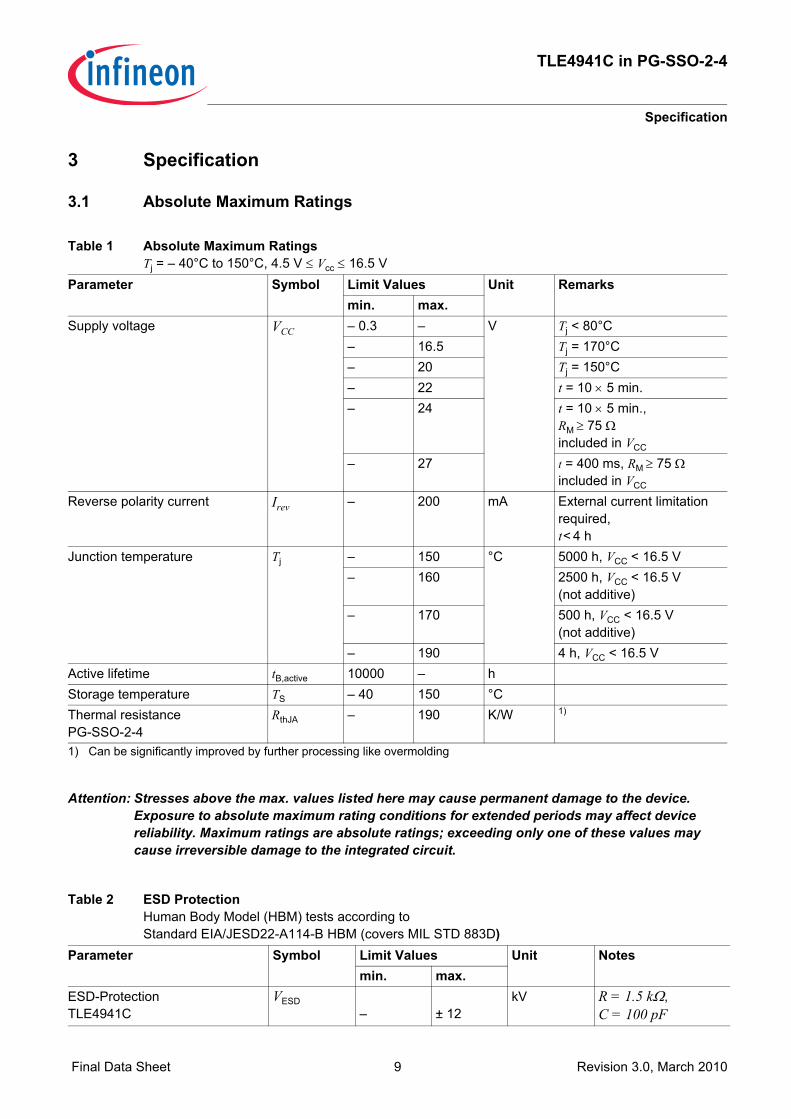
Table 1 Absolute Maximum RatingsTj = – 40°C to 150°C, 4.5 V ≤ Vcc ≤ 16.5 V
Parameter Symbol Limit Values Unit Remarksmin. max.
Supply voltage VCC – 0.3 – V Tj < 80°C– 16.5 Tj = 170°C– 20 Tj = 150°C– 22 t = 10 × 5 min.– 24 t = 10 × 5 min.,
RM ≥ 75 Ωincluded in VCC
– 27 t = 400 ms, RM ≥ 75 Ωincluded in VCC
Reverse polarity current Irev – 200 mA External current limitation required, t< 4 h
Junction temperature Tj – 150 °C 5000 h, VCC < 16.5 V– 160 2500 h, VCC < 16.5 V
(not additive)– 170 500 h, VCC < 16.5 V
(not additive)– 190 4 h, VCC < 16.5 V
Active lifetime tB,active 10000 – hStorage temperature TS – 40 150 °CThermal resistance PG-SSO-2-4
RthJA – 190 K/W 1)
1) Can be significantly improved by further processing like overmolding
Table 2 ESD ProtectionHuman Body Model (HBM) tests according to Standard EIA/JESD22-A114-B HBM (covers MIL STD 883D)
Parameter Symbol Limit Values Unit Notesmin. max.
ESD-ProtectionTLE4941C
VESD– ± 12
kV R = 1.5 kΩ,C = 100 pF

Final Data Sheet 10 Revision 3.0, March 2010
TLE4941C in PG-SSO-2-4
Specification
3.2 Operating Range
Note: Within the operating range the functions given in the circuit description are fulfilled.
Table 3 Operating RangeParameter Symbol Limit Values Unit Remarks
min. max.Supply voltage VCC 4.5 20 V Directly on IC leads;
includes not the voltage drop at RM
Supply voltage ripple VAC – 6 Vpp VCC = 13 V0 < f < 50 kHz
Junction temperature Tj – 40 150 °C– 170 500 h,
VCC ≤ 16.5 V, increased jitter permissible
Pre-induction B0 – 500 + 500 mTPre-induction offset between outer probes
ΔBstat., l/r – 20 + 20 mT
Differential Induction ΔB – 120 + 120 mT

Final Data Sheet 11 Revision 3.0, March 2010
TLE4941C in PG-SSO-2-4
Specification
3.3 Electrical CharacteristicsTable 4 Electrical Characteristics
All values specified at constant amplitude and offset of input signal, over operating range, unless otherwise specified. Typical values correspond to VCC = 12 V and TA = 25°C
Parameter Symbol Limit Values Unit Remarksmin. typ. max.
Supply current ILOW 5.9 7 8.4 mASupply current IHIGH 11.8 14 16.8 mASupply current ratio IHIGH / ILOW 1.9 – –Output rise/fall slew rate TLE4941C
tr, tf 127.5
––
2624
mA/µs RM ≤ 150 ΩRM ≤ 750 ΩSee Figure 4
Output rise/fall slew rate TLE4941C
tr, tf88
––
2226
mA/µsRM = 75 ΩT < 125°CT < 170°CSee Figure 4
Current ripple dIX/dVCC IX – – 90 µA/V only valid for 49411)
1) only valid for TLE4941. For TLE4941C higher values occure and depend strongly on Rm-C combination
Limit threshold1 Hz < f < 2500 Hz2500 Hz < f < 10000 Hz
ΔBLimit0.35–
0.8–
1.51.7
mT 2)
2) Magnetic amplitude values, sine magnetic field, limits refer to the 50% critera. 50% of edges are missing
Initial calibration delay time
td,input – – 300 µs Additional to nstart3)
Magnetic edges required for initial calibration
nstart – 3 64) magn. edges5)
7th edge correct 6)
Frequency f 17)
2500––
250010000
Hz 8)
Frequency changes df/dt – – ± 100 Hz/msDuty cycle duty 40 50 60 % 9)ΔB = 2 mT sin-wave
Def. See Figure 4Jitter, Tj < 150°C Tj < 170°C1 Hz < f < 2500 Hz
SJit-close ––
––
± 2± 3
% 10)1σ valueVCC = 12 VΔB ≥ 2 mT
Jitter, Tj < 150°C Tj < 170°C2500 Hz < f < 10000 Hz
SJit-close ––
––
± 3± 4.5
% 10)1σ valueVCC = 12 VΔB ≥ 2 mT
Jitter, Tj < 150°C Tj < 170°C1 Hz < f < 2500 Hz
SJit-far ––
––
± 4± 6
% 10)1σ valueVCC= 12 V2 mT ≥ ΔB > ΔBLimit
Jitter, Tj < 150°C Tj < 170°C2500 Hz < f < 10000 Hz
SJit-far ––
––
± 6± 9
% 10)1σ valueVCC = 12 V2 mT ≥ ΔB > ΔBLimit
Jitter at board net ripple SJit-AC – – ± 2 % VCC = 13 V ± 6 Vpp0 < f < 50 kHzΔB = 15 mT

Final Data Sheet 12 Revision 3.0, March 2010
TLE4941C in PG-SSO-2-4
Specification
3) Occurrence of Initial Calibration Delay Time td,inputIf there is no input signal (standstill), a new initial calibration is triggered each 0.7 s. This calibration has a duration td,input of max. 300 µs. No input signal change is detected during that initial calibration time. In normal operation (signal startup) the probability of td,input to come into effect is: td,input / time frame for new calibration 300 µs/700 ms = 0.05%. After IC resets (e.g. after a significant undervoltage) td,input will always come into effect.
4) Magnetic Input Signal Extremely Close to a Switching Threshold of PGA (Pragrammable Gain Amplifier) at Signal StartupAfter signal startup generally all PGA switching into the appropriate gain state happens within less than one signal period. This is included in the calculation for nDZ-Start. For the very rare case that the signal amplitude is extremely close to a PGA switching threshold and the full range of following speed ADC respectively, a slight change of the signal amplitude can cause one further PGA switching. It can be caused by non-perfect magnetic signal (e.g. amplitude modulation due to tolerances of pole-wheel, tooth wheel or air gap variation). This additional PGA switching can result in a further delay of the output signal (nDZ-Start) up to three magnetic edges leading to a worst case of nDZ-Start = 9. Due to the low probability of this case it is not defined as max. value in the data sheet.
5) The sensor requieres up to nstart magnetic switching edges for valid speed information after power-up or after a stand still condition. During that phase the output is disabled.
6) One magnetic edge is defined as a montonic signal change of more than 3.3 mT7) only valid in calibrated mode. For entering calibrated mode higher frequencies are necessary.8) High frequency behavior not subject to production test - verified by design/characterization. Frequency above 2500 Hz may
have influence on jitter performance and magnetic thresholds9) During fast offset alterations, due to the calibration algorithm, exceeding the specified duty cycle is permitted for short time
periods10) Not subject to production test verified by design/characterization

Final Data Sheet 13 Revision 3.0, March 2010
TLE4941C in PG-SSO-2-4
Specification
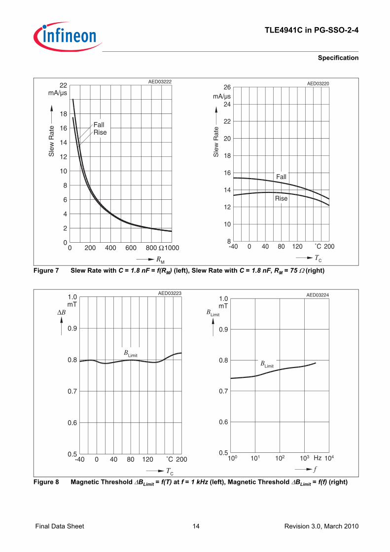
3.4 Typical Diagrams (measured performance)Tc = Tcase, IC = approx. Tj - 5°C
Figure 5 Supply Current = f(T) (left), Supply Current Ratio Ihigh / I Low= f(T) (right)
Figure 6 Supply Current =f(Vcc) (left), Supply Current Ratio Ihigh / I Low=f(Vcc) (right)
-40 1.8
T C
I HIGH / I LOW
1.9
2.0
2.1
2.2
2.3
2.4
0 40 80 120 °C 200
AED03216
-406
TC
IHIGH, ILOW
8
10
12
14
16
18mA
0 40 80 120 ˚C 200
AED03215
IHIGH
ILOW
I HIGH
I LOW
0 6
V CC
I HIGH , I LOW
mA
5 10 15 20 V 30
AED03217
25
8
10
12
14
16
20
IHIGH / ILOW
IHIGH / ILOW
01.6
VCC
5 10 15 20 V 30
AED03218
25
1.8
2.0
2.2
2.4
Final Data Sheet 14 Revision 3.0, March 2010
TLE4941C in PG-SSO-2-4
Specification
Figure 7 Slew Rate with C = 1.8 nF = f(RM) (left), Slew Rate with C = 1.8 nF, RM = 75 Ω (right)
Figure 8 Magnetic Threshold ΔBLimit = f(T) at f = 1 kHz (left), Magnetic Threshold ΔBLimit = f(f) (right)
Rise
Fall
-408
TC
0 40 80 120 ˚C 200
AED03220
Sle
w R
ate
mA/µs
10
12
14
16
18
20
22
24
26
00
RM
AED03222
Sle
w R
ate
mA/µs
200 400 600 800 1000Ω
2
4
6
8
10
12
14
16
18
22
FallRise
1000.5
f
BLimit
AED03224
mT
0.6
0.7
0.8
0.9
1.0
Hz101 102 103 104
BLimit
-400.5
TC
ΔB
0 40 80 120 ˚C 200
AED03223
BLimit
mT
0.6
0.7
0.8
0.9
1.0

Final Data Sheet 15 Revision 3.0, March 2010
TLE4941C in PG-SSO-2-4
Specification
Figure 9 Jitter 1σ at ΔB = 2 mT at 1 kHz (left), Delaytime td (right) 1)
1) td is the time between the zero crossing of ΔB = 2 mT sinusoidal input signal and the rising edge (50%) of the signal current.
-400
TC
0 40 80 120 ˚C 200
AED03225
Jitte
r
%
0.1
0.2
0.3
0.4
0.5
0.6
0.7
0.8
0.9
-400
TC
˚C
AED03226
0 40 80 120 180
td
2
4
6
8
10
12
µs
td @ 2.5 kHz

Final Data Sheet 16 Revision 3.0, March 2010
TLE4941C in PG-SSO-2-4
Specification
3.5 Electro Magnetic Compatibility (EMC)
Table 5 Electro Magnetic Compatibility (values depend on RM!) Ref. ISO 7637-1; test circuit 1;ΔB = 2 mT (amplitude of sinus signal); VCC = 13.5 V, fB = 100 Hz; T = 25°C; RM ≥ 75 Ω
Parameter Symbol Level/Typ StatusTestpulse 1Testpulse 2Testpulse 3aTestpulse 3bTestpulse 4Testpulse 5
VEMC IV / – 100 VIV / 100 VIV / – 150 VIV / 100 VIV / – 7 VIV / 86.5 V1)
1) Applying in the board net a suppressor diode with sufficient energy absorption capability
C2)
C2)
AAB3)
C
2) According to 7637-1 the supply switched “OFF” for t = 200 ms3) According to 7637-1 for test pulse 4 the test voltage shall be 12 V ± 0.2 V. Measured with RM = 75 Ω only. Mainly the currentconsumption will decrease. Status C with test circuit 1
Note: Values are valid for all TLE4941C/42C types!
Ref. ISO 7637-3; test circuit 1;ΔB = 2 mT (amplitude of sinus signal); VCC = 13.5 V, fB = 100 Hz; T = 25°C; RM ≥ 75 Ω
Parameter Symbol Level/Typ StatusTestpulse 1Testpulse 2Testpulse 3aTestpulse 3b
VEMC IV / – 30 VIV / 30 VIV / – 60 VIV / 40 V
AAAA
Note: Values are valid for all TLE4941C/42C types!
Ref. ISO 11452-3; test circuit 1; measured in TEM-cellΔB = 2 mT; VCC = 13.5 V, fB = 100 Hz; T = 25°C
Parameter Symbol Level/Typ RemarksEMC field strength ETEM-Cell IV / 250 V/m AM = 80%,f = 1 kHzNote: Only valid for C-types!

Final Data Sheet 17 Revision 3.0, March 2010
TLE4941C in PG-SSO-2-4
Specification
Figure 10 EMC Test Circuit 1
AES03199
GND
VCCSensor
RM C2
VEMC
EMC-Generator MainframeD1
C1D2
Components: D1: 1N4007 or higherD2: T 5Z27 1JC1: 10 µF / 35 VC2: 1 nF / 1000 VRM: 75 Ω / 5 W

Final Data Sheet 18 Revision 3.0, March 2010
TLE4941C in PG-SSO-2-4
Package Information
4 Package InformationPure tin covering (green lead plating) is used. Leadframe material is Wieland K62 (UNS: C18090) and containsCuSn1CrNiTi. Product is RoHS (restriction of hazardous substances) compliant when marked with letter G in frontor after the data code marking and may contain a data matrix code on the rear side of the package (see alsoinformation note 136/03). Please refer to your Key account team or regional sales if you need further information.
Figure 11 Distance Chip to Upper Side of IC
.
d=0.3±0.08mmDistance chip to front side (date code) of IC

Final Data Sheet 19 Revision 3.0, March 2010
TLE4941C in PG-SSO-2-4
Package Information
4.1 Package Outline
Figure 12 PG-SSO-2-4 (Plastic Single Small Outline Package); Dimensions in mm
4.2 PackingYou can find all of our packages, sorty of packing and others in our Infineon Internet Page “Products”: http://www.infineon.com/products.
6.35±0.4
12.7±0.3
±0.34
CODE
1 x 45˚
12.7±1
CODE CODE
-0.11
0.25±0.05
7˚ 7˚
0.2+0.1
Adhesive
±0.5
61
-1
±0.5
18
Tape
0.39±0.1
-0.150.25
9
±0.5
23.8
+0.7
5-0
.5 38 M
AX
.
0.65
3.38
3.71
(0.2
5)±0
.1
±0.0
8
±0.0
6
1.9 MAX.
5.16±0.08
5.34 ±0.05
0.1
MA
X.
1.9 MAX.
1.2±
0.1
±0.050.87±0.051.67
(14.
8)
1)
3.01
2.54
2 A
A
B
1) No solder function area
Total tolerance at 10 pitches ±1
(Use
able
Len
gth)
±0.0
52
2
1.5±0.05
(2.4)
(2.7)
(1.3
)
5.34±0.05
Tape
1.81±0.05
0.2 2x
2x0.51.2 ±0.05
5.16 ±0.08
A - A
A A
Capacitor
(8.1
7) ±0.1
7.07
10.2
±0.1
±0.050.25
0.2 B
±1˚
1 2
0.2
0.1
2x
