tm burn-in & test socket workshop · burn-in & test socket workshop session 7 wednesday...
TRANSCRIPT

Burn-in & TestSocket Workshop
ARCHIVE
March 7 - 10, 2004Hilton Phoenix East / Mesa Hotel
Mesa, Arizona
TM

Burn-in & Test SocketWorkshop
COPYRIGHT NOTICE• The papers in this publication comprise the proceedings of the 2004
BiTS Workshop. They reflect the authors’ opinions and are reproducedas presented , without change. Their inclusion in this publication doesnot constitute an endorsement by the BiTS Workshop, the sponsors,
BiTS Workshop LLC, or the authors.
• There is NO copyright protection claimed by this publication or theauthors. However, each presentation is the work of the authors and
their respective companies: as such, it is strongly suggested that anyuse reflect proper acknowledgement to the appropriate source. Anyquestions regarding the use of any materials presented should be
directed to the author/s or their companies.
• The BiTS logo and ‘Burn-in & Test Socket Workshop’ are trademarksof BiTS Workshop LLC.
TM

Burn-in & Test SocketWorkshop
Session 7Wednesday 3/10/04 8:00AM
DEFORMATION AND CONTAMINATION
“Effects Of Contaminants On Test Pad Surfaces”Therese Souza – Rika Denshi America, Inc.
“Effects Of Solder Ball Deformation On Interconnect QualityAnd Reliability”
John Caldwell – Micron Technology, Inc.
“Testing Of VQFN With Palladium Cobalt Pogo Pin”Thuan-Lian Chua – Infineon Technologies
Jayachandrian – Infineon Technologies Dieter Schuetz – Infineon Technologies
Technical Program

Effects ofContaminants on Test
Pad SurfacesIdentifying A Potential for Yield Loss
Author:Therese Souza, Rika Denshi America
BiTS Workshop 2004

Historical• Contamination recognized as a problem by Bell
Labs
– Problem identified in assembled products
• Separable connectors and wiping effectiveness
– Displacing contamination
– Complicates contact design
• A real & serious problem for microelectronics

Possible Contaminants
• Handling – skin oils, flakes of skin, smoke, dust
• Packaging – residues from plastic bags
• Process chemicals – plating residues, solder flux,tap water, cleaners, oils, outgassing from plasticfixtures
• Storage & environmental gases - hydrocarbons,sulfides

Challenge for Contactors
Smaller test probes have decreased surface area,normal force, and operating/testing voltages.
These factors lead to:Increase in sensitivity to surface contamination

Symptoms of Contamination
• Failure or erratic data at electrical testing
• May pass initial testing but fail at a later date
Note: In each case the product passes tests after cleaning
Example using resistance measurements:
• Initial resistance is high or erratic – decreases withcycling or with increased normal force

Opportunity lost per 1,000,000 devices tested
Yield Loss, 0.1%
100,000100
500,000500
750,000750
1,000,0001000
Opportunity Lost, $Cost of Device, $

Experiment
• 50 test probes
• 50 cycles per test
• 7 test samples (blocks)
• Resistance before and
after contaminating test
samples
• Contact force 62 grams
• Plunger tips cleaned
• Based on ASTM B667-97
• Cannot prevent vibrations

ASTM B667-97• 4-wire contact
resistance method
• Effects of films onconductive surfaces
• No wipe or vibrations
• Produce normal forcevs. resistance curve

Cycle Tester

Selected ContaminantsApplied to Test Surface (Block)
Test Surface has a copper base plated with 1 micronof nickel then .75 micron of hard gold.
1. Tap Water2. Skin Oils3. Dust4. Storage in Plastic Bag, 24 hours, 100
oF
5. No Clean Flux (ORL-O), 250 oC, 5 minutes
6. Cigarette Smoke7. Control – not contaminated

Before Contamination
Initial Resistance Readings at Start
0
10
20
30
40
50
60
70
1 5 9 13 17 21 25 29 33 37 41 45 49
Probe Number
Mill
iOhm
s
1234567

After Contamination
Resistance After Contamination
0
20
40
60
80
100
120
140
160
1 5 9 13 17 21 25 29 33 37 41 45 49
Plunger Number
Mill
iOhm
s
1234567

After Contamination
Comparison Average Resistance Readings
0
5
10
15
20
25
30
35
40
45
tapwater
skin oils dust plasticbag
flux smoke control
Mill
iOhm
s
BeforeAfter
Std Dev between 0.72-2.05 MilliOhms
Open Circuit on one contact with dust

Cleaning
• Identify the contaminant– ESCA, Auger… etc
• Test several cleaners or processes.– Do not assume that a cleaner is “safe”
and will not leave contaminants
• Plasma cleaning
• Vacuum instead of high pressure air

Contamination Prevention• Prevention is better than repair• Program that:
– Identifies potential sources of contamination
– Includes process steps that prevent or repaircontamination
– Routine testing for clean surface
• UV lights
• Ionic contamination testing

Conclusions
• Surface contamination can affect electrical testing
• Potential contaminants can be identified
• Contamination can be prevented with a proactive plan
• Repair is possible with right process

References• Robert S. Mroczkowski, Electronic Connector
Handbook, McGraw-Hill 1998
• Outgassing of Engineering Plastics In High-VacuumApplications, http://www.boedeker.com/outgas.htm
• H. W. Hermance and T. F. Egan, “Organic Deposits onPrecious Metal Contacts”, The Bell System TechnicalJournal, May 1958, pp 739-776.

References
• T. F. Egan, Ionic Contamination, Plating, April 1973
• Rinsewater Quality....Hard Data,http://www.pcbfab.com/rinsew.html
• Piet van Dijk, Critical Aspects of Electrical ConnectorContacts;http://www.pvdijk.com/images/21thiceccriticalaspects.pdf

John CaldwellTest R&D Engineer
Micron Technology, Inc.
Effects of Grid Array Ball Deformationon Solder Joint Quality and Reliability
2004 Burn-In and Test Socket WorkshopMarch 7�10, 2004

2
Agenda
►Industry concerns & opposingarguments►The “No Contact Zone”►Design of experiment►Device coplanarity►Solder joint quality and reliability►Follow-on research►Q&A

3
Background►Industry concerns
! Entrapped flux and contaminates may cause voids in theBGA solder joint during SMT reflow
! Deformation on the upper hemisphere of the solder ballmay cause coplanarity error
! Cosmetics (??)►Opposing arguments
! Solder ball contamination/residual flux, PCB landcontamination, reflow oven profile, and solder paste/fluxchemistry have a profound impact on voiding [1]
! Voided solder joints have been shown to perform betterduring reliability testing [2]
►Bottom line: The surface mount process MUST bedone right

4
The “No Contact Zone”►Some semiconductor producers adhere to a
“no contact zone” policy! Require test socket suppliers to provide
alternate solution! Semiconductor producers may address within their
own process (i.e. post electrical test reflow)►Is this really necessary?
Ball Grid Array Device
Typical “NoContact Zone”

5
Design of Experiment►SDRAM devices contacted repeatedly, then
segregated into “damage level” groups! Sample set = 300 SDRAM fBGA�s per damage group! One �contact� = One insertion into each of the three
contact styles (crown, cup, pincher)►Device packages laser scanned for packaged
component dimensions (coplanarity, etc.)►Damage level groups randomized and assembled
onto dual in-line memory modules (DIMM)►Initial module failures investigated for possible
correlation to preexisting solder damage►Passing modules reliability tested up to 3,250
temperature cycles►Failure verification post temperature cycle

6
Materials & Process
0.8mmPitch:
0.40mmSolder Ball Diameter:
Board-on-Chip (BOC)Device Package:
63% Tin/37% LeadSolder Composition:
Eutectic Solder PastePCB Attach Medium:
Standard (215°C peak)Reflow Profile:
0.33mmLand Pad Diameter:
60Solder Balls:8 x 16Device Size (mm):

7
Build & Test Parameters
►Memory module! 8-component DIMM! 6-layer FR4! PCB thickness = 1.27mm! PCB length = 133.35mm! PCB height = 31.75mm
►System level motherboard test to gauge time-zero module quality
►Reliability test! -40°C to +85°C, air-to-air, two cycles per hour

8
Excessive Solder Deformation?

9
Levels of Deformation
►Low: control►Medium: up to 24 insertions►High: up to 50 insertions

10
Device Coplanarity
►Laser scandata analyzedstatistically
►No adverseimpact
Oneway Analysis of Coplanarity (mm) By Group
1_LOW2_MED3_HIGH
Level 3000 3000 3000
Number0.0199300.0185530.016877
Mean0.0113340.0106360.009727
Std Dev0.000210.000190.00018
Std Err Mean0.019520.018170.01653
Lower 95%0.020340.018930.01723
Upper 95%
Means and Std Deviations
Cpl
nr (m
m)
0
0.01
0.02
0.03
0.04
0.05
0.06
1_LOW 2_MED 3_HIGH
Group
Each PairStudent's t 0.05

11
Time-Zero Module Quality
►6 component failures! Internal component degradation! Consistent with silicon level defects
►2 component failures! Poor solder joint geometry! Low volume solder interconnect! No voids
►X-ray, x-section, electrical failureanalysis to verify failure modes
►Time-zero module fails notrelated to solder damage/voids

12
Solder Joint Reliability (-40°C to +85°C)
Source: Micron Technology, Inc.
6000.001000.001.00
5.00
10.00
50.00
90.00
99.00 0.9
1.0
1.2
1.4
1.6
2.0
3.0
6.0
βη
Probability - Weibull
Thermal Cycles, (t)
Unr
elia
bilit
y, F
(t)
1/26/2004 15:35Micron T echnologyJohn Caldwell
WeibullMC/HighW2 RRX - SRM MED
F=28 / S=0
β1=6.3121, η1=3477.0726, ρ=0.9878
MC/LowW2 RRX - SRM MED
F=31 / S=0
β2=7.5691, η2=3309.2888, ρ=0.9882
MC/MedW2 RRX - SRM MED
F=39 / S=0
β3=6.4851, η3=3417.0370, ρ=0.9874

13
Conclusion►Surface mount process maturity and monitoring
is VERY important! X-ray (void volume & frequency)! X-section (standoff height measurements)! Reflow oven profile! Solder paste/flux chemistry! Clean BGA solder alloys & PCB land pads
►No correlation between degree of solder balldamage and -! Component coplanarity degradation! Time-zero solder interconnect quality! Solder joint reliability (SJR)

14
Follow-on Research►96.5Sn/3.0Ag/0.5Cu (lead-free) versus
62Sn/36Pb/2.0Ag►Daisy chain WLCSP�s►In-situ solder joint monitoring
►Results " April 2004
Pb-Free Pb

15
Acknowledgements & Sources► Special thanks to:
William Casey, Mike Morrison, John Odle, Faye Sinclair,Rich Mansfield, David Sammons, Glen Watson,Gregory Barnett, Ismat Sulaivany, Syed Ahmad, KenEytchison, Von Sorenson, Arlene Haugse
► Effects of solder joint voiding on plastic ball gridarray reliability
Donald R. Banks, et al.Motorola Semiconductor Products Sector
► Reduction of voiding in eutectic ball grid arraysolder joints
William CaseyMicron Technology, Inc.

Q & A

Page 1
2004 Burn-in and Test Socket WorkshopTesting of VQFN with Palladium-Cobalt Pogo Pin
Testing of VQFN with Palladium-Cobalt Pogo Pin
Chua Thuan Lian
Jayachandrian
Schuetz Dieter

Page 2
2004 Burn-in and Test Socket WorkshopTesting of VQFN with Palladium-Cobalt Pogo Pin
Contents
Background
Problem
Target
Introduction to Testing of VQFN Package
Study the Poor Performance of the Gold PogoPins
Pogo Pins Selection and Study
Result of the Performance of the PdCo Pogo Pins
Benifits of Introduction of PdCo Pogo Pins

Page 3
2004 Burn-in and Test Socket WorkshopTesting of VQFN with Palladium-Cobalt Pogo Pin
Low Production OutputCapacity
High Invalid Test Failures
High Tester/HandlerDowntime due to frequent
cleaning of contactors
High Consumption ofPogo Pins
VQFN 48Testing

Page 4
2004 Burn-in and Test Socket WorkshopTesting of VQFN with Palladium-Cobalt Pogo Pin
Solder debris on tipsafter 12k insertionNew crown tip pogo pins
1. Short life-span of pogo pins due to deposition of solder onthe pin (<12k insertions).
2. High downtime due to regular cleaning of pogo-pins.3. High % of invalid parametric failures (12% ~ 40%) .
Hmm… Let’s see the condition of the pogo pins
Page 5
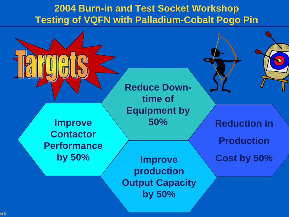
2004 Burn-in and Test Socket WorkshopTesting of VQFN with Palladium-Cobalt Pogo Pin
Reduce Down-time of
Equipment by50%Improve
ContactorPerformance
by 50% Improveproduction
Output Capacityby 50%
Reduction in
Production
Cost by 50%

Page 6
2004 Burn-in and Test Socket WorkshopTesting of VQFN with Palladium-Cobalt Pogo Pin

Page 7
2004 Burn-in and Test Socket WorkshopTesting of VQFN with Palladium-Cobalt Pogo Pin
Introduction to Very thin Quad Flat Non Leaded Package (VQFN)
Mold side view of VQFN 48 Pad side view of VQFN 48
Package Body size (mm)
Package thickness (mm)
Terminal pitch (mm)
Status
VQFN 48 7 x 7 In production VQF N 40 5.5 x 6.5 In production VQFN 32 4.5 x 5.5 Q4/ 2004 VQFN 24 3.5 x 4.5 Q2/ 2004 VQFN 20 3.5 x 3.5
0.9
0.5
In production

Page 8
2004 Burn-in and Test Socket WorkshopTesting of VQFN with Palladium-Cobalt Pogo Pin
Pogo pin contact element
IC Contact pad
Pogo pin Contact element
Solder ball
Test Contacting Methodology
VQFN Package
Ball Grid ArrayPackage
MT ‘C’ shape contactelement
DUT board-contactelement interface
IC leadContact element
Leaded Package

Page 9
2004 Burn-in and Test Socket WorkshopTesting of VQFN with Palladium-Cobalt Pogo Pin
VQFN package contact elementPogo-pins are used as contacting elements betweendevice and DUT board.
Pogo pins
IC Contact pad
size of pad
0.55
0.250.25
0.5

Page 10
2004 Burn-in and Test Socket WorkshopTesting of VQFN with Palladium-Cobalt Pogo Pin
Test Handling TechnologyGravity handlers are used to test VQFN 48-1 packagesby means of pogo pin contactors.
Test
Crown tip pogo pins from RXX
The initial pogo pin design used was the crown tip pogo pins.

Page 11
2004 Burn-in and Test Socket WorkshopTesting of VQFN with Palladium-Cobalt Pogo Pin

Page 12
2004 Burn-in and Test Socket WorkshopTesting of VQFN with Palladium-Cobalt Pogo Pin
Vxx pogo pin
Nxx pogo pin
Rxx pogo pin
• Study of the gold plated pogopin from different supplier.
• Solder deposit were confirmedon all evaluated gold platedplate.
Gold Plated Pogo Pins

Page 13
2004 Burn-in and Test Socket WorkshopTesting of VQFN with Palladium-Cobalt Pogo Pin
New Pogo pin Pogo pin at 100K insert
• Study of the electrical impact on the solderdeposit on the tip surface.
• Increase of resistance is observed as earlyafter 1K insertion. And worst at 10K
Gold Plated Pogo Pins

Page 14
2004 Burn-in and Test Socket WorkshopTesting of VQFN with Palladium-Cobalt Pogo Pin
Experiments shows that as solder deposition increases, the contactresistance will also increase.
Significant increase in contact
resistance after 10k insertions
Increase in contact resistance of pogo pins will lead to high% of invalid parametric failures.
Touchdowns - DC Resistance (Average)
Touchdowns
Res
ist a
nce
( mO
hm)
Gold Plated Pogo Pins

Page 15
2004 Burn-in and Test Socket WorkshopTesting of VQFN with Palladium-Cobalt Pogo Pin
Pogo pin before cleaning Pogo pin after cleaning
• Study of the impact of cleaning on gold plated pogo pin.• Solder deposit was able to be remove after cleaning.• Pogo pin based was exposed after freq cleaning
Gold Plated Pogo Pins

Page 16
2004 Burn-in and Test Socket WorkshopTesting of VQFN with Palladium-Cobalt Pogo Pin
Adhesive Mode Abrasive Mode
Solder
Pin Pin
• Study of the mode of the gold plating removal.• Adhesive effect of gold plating removal was observed after freq
cleaning
Base Material
Gold Plated Pogo Pins
Page 17
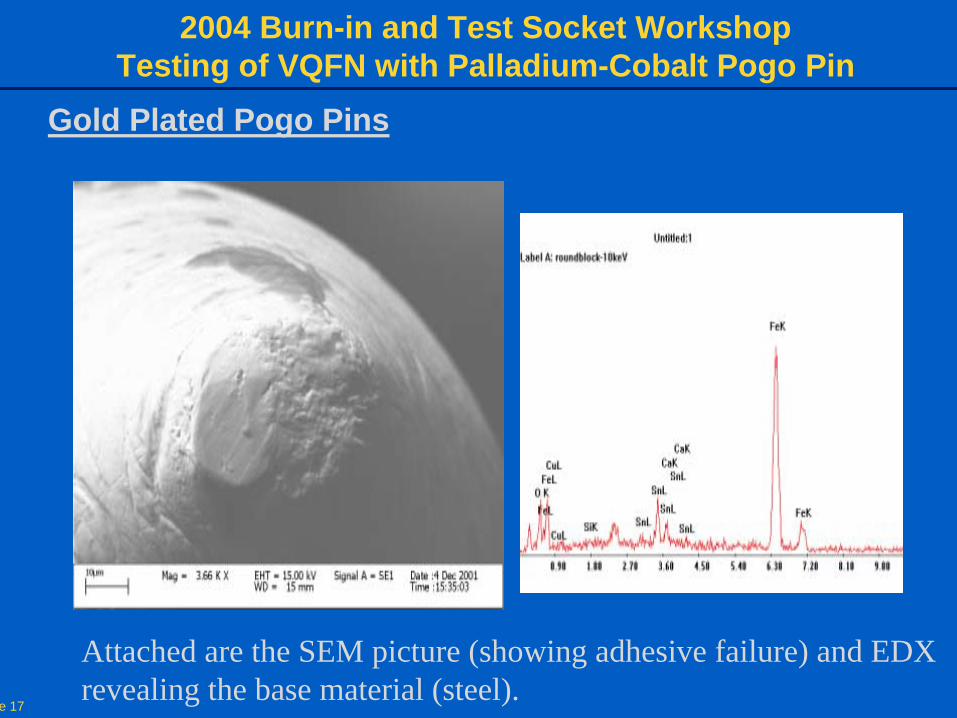
2004 Burn-in and Test Socket WorkshopTesting of VQFN with Palladium-Cobalt Pogo Pin
Attached are the SEM picture (showing adhesive failure) and EDXrevealing the base material (steel).
Gold Plated Pogo Pins

Page 18
2004 Burn-in and Test Socket WorkshopTesting of VQFN with Palladium-Cobalt Pogo Pin
Finding of the problem
• The solder deposit, which has an adhesive effect on the pogo
pins, has caused an increase in the contact resistance of the pins.
•The same adhesive effect was observed in the various types of
pogo pins used for the VQFN packages.
•Cleaning is needed to remove the solder deposit from the pogo
pins, but this will cause a deterioration in the life-span of the
pogo pins.

Page 19
2004 Burn-in and Test Socket WorkshopTesting of VQFN with Palladium-Cobalt Pogo Pin

Page 20
2004 Burn-in and Test Socket WorkshopTesting of VQFN with Palladium-Cobalt Pogo Pin
• Mechanical life cycle test (Contact element life)
• Mechanical performance ( Test pad protection,
DUT board)
• Electrical performance (True test monitoring)
Test contactor qualification test
•Reliable and Good Electromechanical Performance
•Long Life-span, >500k Insertions
•Robust Housing, > 1million insertions
•Modular Design for Ease of Maintenance
•Low Cost
Main criteria for the selection of test contactorSelection criteria and Study Method
• Mechanical requirements ( Cleaning, contact
replacement)

Page 21
2004 Burn-in and Test Socket WorkshopTesting of VQFN with Palladium-Cobalt Pogo Pin
• Look into different material or plating with better solderresistance property
• Conduct cycle test to check on insertion life cycle vs resistance
• Conduct contact housing evaluation with actual productionloading
• To compare the Operating mechanism of pogo pin
Selection criteria and Study Method

Page 22
2004 Burn-in and Test Socket WorkshopTesting of VQFN with Palladium-Cobalt Pogo Pin
Cycle Testing

Page 23
2004 Burn-in and Test Socket WorkshopTesting of VQFN with Palladium-Cobalt Pogo Pin
Rika Denshi Au-Pin
0
0.5
1
1.5
2
2.5
3
3.5
4
4.5
0 5000 10000 15000 20000 25000 30000
# touchdowns
resi
stan
ce (o
hms)
8020SnPb_standard_AUpin8020_SnPb_reflow_Au_Pin100Sn_standard_Au_Pin100Sn_shiny_Au_Pin98_2SnBi_Au_Pin
Life Cycle Resistance StudyGold Pin

Page 24
2004 Burn-in and Test Socket WorkshopTesting of VQFN with Palladium-Cobalt Pogo Pin
Ni_Pin_on 80_20SnPb_Standard
0
0.5
1
1.5
2
2.5
3
3.5
4
4.5
5
0 5000 10000 15000 20000 25000 30000
# touchdowns
resi
stan
ce (o
hms)
8020_SnPb_standard_Ni_Pin80_20SnPb_Standard_Synergetix_Ni_Pin
Life Cycle Resistance Study

Page 25
2004 Burn-in and Test Socket WorkshopTesting of VQFN with Palladium-Cobalt Pogo Pin
Rika Denshi PaCo-Pin
0
0.5
1
1.5
2
2.5
3
3.5
4
4.5
0 5000 10000 15000 20000 25000 30000
# touchdowns
resi
stan
ce (o
hms)
8020_SnPb_standard_PdCo_pin8020_SnPb_reflow_Pd_CO_pin100Sn_standard_PdCo_Pin
Life Cycle Resistance Study
PdCo Pin

Page 26
2004 Burn-in and Test Socket WorkshopTesting of VQFN with Palladium-Cobalt Pogo Pin
Contact resistance
0
0.5
1
1.5
2
2.5
3
3.5
4
4.5
5
0 5000 10000 15000 20000 25000 30000
# touchdownes
resi
stan
ce [O
hms]
8020_SnPb_standard_PdCo_pin8020SnPb_standard_AUpin8020_SnPb_reflow_Au_Pin8020_SnPb_reflow_2_PaCo_pin
Life Cycle Resistance Study
Contact resistance vs Standard and reflow

Page 27
2004 Burn-in and Test Socket WorkshopTesting of VQFN with Palladium-Cobalt Pogo Pin
Contact resistance Pogo-Pins vs. Leadframe with different Platings
0
0.5
1
1.5
2
2.5
3
3.5
4
4.5
5
0 5000 10000 15000 20000 25000 30000
# touchdowns
resi
stan
ce [O
hms]
80/20 SnPb standard (PdCo Pin)80/20 SnPb standard (Au-Pin)80/20 SnPb reflow (Au-Pin)80/20 SnPb reflow (PdCo Pin)80/20 SnPb standard (Ni-Pin)100 Sn standard (Au-Pin)100 Sn standard (PdCo-Pin)100 Sn shiny (Au-Pin)
Life Cycle Resistance Study

Page 28
2004 Burn-in and Test Socket WorkshopTesting of VQFN with Palladium-Cobalt Pogo Pin
Contactor Evaluation Matrix
2Good Elect. Yield. Life Span~200K.Rasco“X” Source
(250K)Rasco
1Good Elect. Yield. Life Span>500K*K&SK&S (500K)Multitest
1Good Elect. Yield. Life Span>500K*K&SK&S (500K)Rasco
3High Parametric Failures whenreaching end of life span*SNR“X” Source
(250K)Multitest
3High Parametric Failures whenreaching end of life spanMultitest“X” Source
(250K)Multitest
CleaningFreq
ResultHousingPin TypeHandlerType
Note: 1. * denotes design based on Infineon Outline. 2. Material used for pogo pins is Palladium Cobalt.

Page 29
2004 Burn-in and Test Socket WorkshopTesting of VQFN with Palladium-Cobalt Pogo Pin
“X” source Pogo pin (Single Acting)Comparison of “X” Source and K&S Pogo-pin Operating Mechanism
DUT Board
Device Only DUT-end spring loaded(Spring force19g)
DUT Board
Both ends spring loaded (reciprocating)(Spring Force 42g)
0.3mm pre-load
K&S Pogo pin (Double Acting)
Pogo-pin housingPlunger (fixed-End)
HandlerPlunger
Only the plunger-tip moves whendevice is plunged
Barrel
The Plunger and the barrel movestogether when device is plunged
Pre-load ensures goodcontinuitybetween DUT board and pins,reduces damage to test pads
Higher contact force on package pads improveselectrical performance
Less friction during reciprocating action

Page 30
2004 Burn-in and Test Socket WorkshopTesting of VQFN with Palladium-Cobalt Pogo Pin
Summary of the Study of PdCo• The PdCo plated pogo pin has longer insertion life-span and
minimum change in contact resistance, relative to large number ofinsertions
• PdCo plating exhibits low coefficient of friction and makes it easierfor foreign matter to slide along the surface of the plunger andprevents solder deposition
• Contactor design also plays a key role in the insertion life cycleperformance
• Contactor with Pre-load design also reduces damage to test padsthrough good continuity between DUT board and pins
• Minimum cleaning frequency during production is achieved.
• PdCo plated pogo pins are suitable for testing of VQFN package

Page 31
2004 Burn-in and Test Socket WorkshopTesting of VQFN with Palladium-Cobalt Pogo Pin

Page 32
2004 Burn-in and Test Socket WorkshopTesting of VQFN with Palladium-Cobalt Pogo Pin
clean freq Output % Invalid
Fus18/16/18 Test performance
0
10
20
30
40
50
31-D
ec
2-Ja
n
4-Ja
n
6-Ja
n
8-Ja
n
10-J
an
12-J
an
14-J
an
16-J
an
18-J
an
20-J
an
22-J
an
24-J
an
26-J
an
28-J
an
30-J
an
1-Fe
b
3-Fe
b
5-Fe
b
7-Fe
b
9-Fe
b
11-F
eb
13-F
eb
15-F
eb
17-F
eb
19-F
eb
21-F
eb
23-F
eb
Clea
ning
Fre
quen
cy
0
7
14
21
28
35
Out
put (
K)In
valid
Fai
ls (%
)
Actual Production Monitoring
PdCo plated
pins (K&S)
Ni plated
pins

Page 33
2004 Burn-in and Test Socket WorkshopTesting of VQFN with Palladium-Cobalt Pogo Pin
Life-Span(No.of insertions)
Avg Daily Production Output
500,000
2
14,000
Vendor’s Spec.Cleaning Freq./Day
500,000
Gold platedpogo-pins
50,000
48
7,000
100,000
Characteristics
% Invalid Test FailuresAvg 1st Pass Yield 90 - 94%70 - 75%
< 5%12 - 40%
(PdCo) plated pogo-pins

Page 34
2004 Burn-in and Test Socket WorkshopTesting of VQFN with Palladium-Cobalt Pogo Pin

Page 35
2004 Burn-in and Test Socket WorkshopTesting of VQFN with Palladium-Cobalt Pogo Pin
Cost of pins Consumed/Yr
Cost Savings/set-upCost Savings/set-upCost of Pogo-pinsNickel plated pins : S$ XX.XXPalladium Plated pins : S$ YY.YY
AssumptionOutput / day : 14,000Package : VQFN 48 (48 pins/set-up)
Life-Span(No.of insertions)
Palladium Cobaltplated pogo-pins
250,000
S$974
S$11,688
Cost of pins consumed/month
Savings per year S$76,440 (S$88,128 - S$11,688)
Gold platedpogo-pins
50,000
S$7,344
S$88,128 [S$7,344 x 12mths] [S$974 x 12mths]
Characteristics
86% Savings
Results (Quantifiable)

Page 36
2004 Burn-in and Test Socket WorkshopTesting of VQFN with Palladium-Cobalt Pogo Pin
Results (Quantifiable)
Cost impact on handlerdowntime/day(per year)
Cost Savings/set-upCost Savings/set-up
No.of cleaning/day
Palladium Cobaltplated pogo-pins
2
S$8,294
S$2,527
Down Time/dayDue to cleaning
Cost impact on tester Downtime/ per year
Savings per year S$248,900 (199065+60652) - (8294+2527)]
10 mins [2 x 5mins]
Gold platedpogo-pins
48
S$199,065
S$60,652
[48cleaning x 5mins]240mins
Characteristics
Total savingsper year
SGD 325,340
95% Savings

Page 37
2004 Burn-in and Test Socket WorkshopTesting of VQFN with Palladium-Cobalt Pogo Pin
Benefits
Reduction inProduction Cost
Increased incontactor
performance
Increased inProduction output
Reduction inDowntime ofEquipment

Page 38
2004 Burn-in and Test Socket WorkshopTesting of VQFN with Palladium-Cobalt Pogo Pin