tms320dm6435 digital media processor - ti.com
TRANSCRIPT
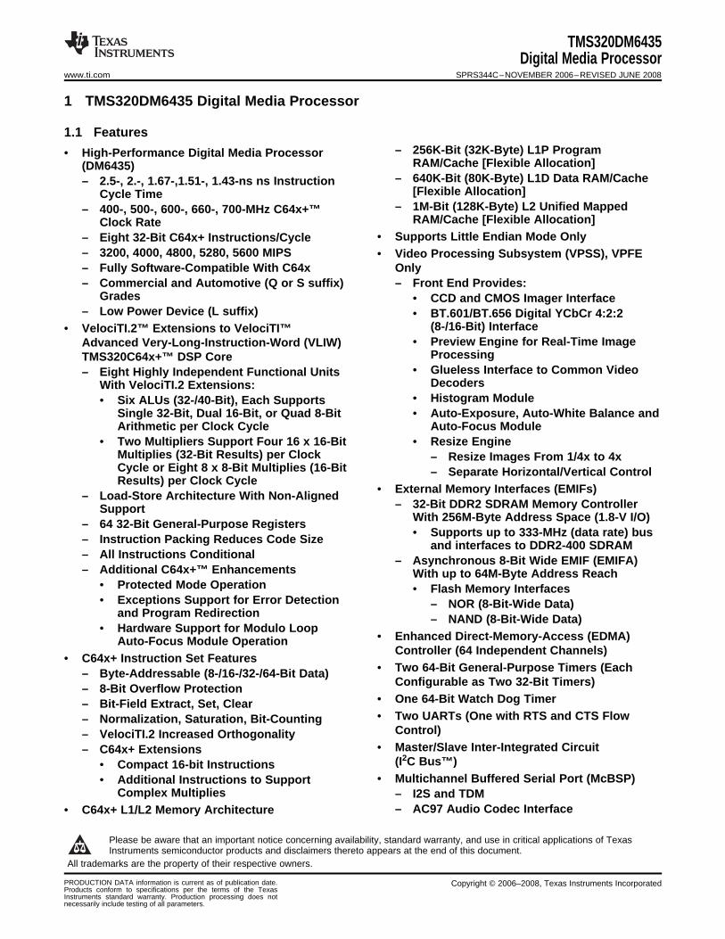
1 TMS320DM6435 Digital Media Processor
1.1 Features
TMS320DM6435Digital Media Processor
www.ti.com SPRS344C–NOVEMBER 2006–REVISED JUNE 2008
– 256K-Bit (32K-Byte) L1P Program• High-Performance Digital Media ProcessorRAM/Cache [Flexible Allocation](DM6435)
– 640K-Bit (80K-Byte) L1D Data RAM/Cache– 2.5-, 2.-, 1.67-,1.51-, 1.43-ns ns Instruction[Flexible Allocation]Cycle Time
– 1M-Bit (128K-Byte) L2 Unified Mapped– 400-, 500-, 600-, 660-, 700-MHz C64x+™RAM/Cache [Flexible Allocation]Clock Rate
• Supports Little Endian Mode Only– Eight 32-Bit C64x+ Instructions/Cycle– 3200, 4000, 4800, 5280, 5600 MIPS • Video Processing Subsystem (VPSS), VPFE– Fully Software-Compatible With C64x Only– Commercial and Automotive (Q or S suffix) – Front End Provides:
Grades • CCD and CMOS Imager Interface– Low Power Device (L suffix) • BT.601/BT.656 Digital YCbCr 4:2:2
(8-/16-Bit) Interface• VelociTI.2™ Extensions to VelociTI™• Preview Engine for Real-Time ImageAdvanced Very-Long-Instruction-Word (VLIW)
ProcessingTMS320C64x+™ DSP Core• Glueless Interface to Common Video– Eight Highly Independent Functional Units
DecodersWith VelociTI.2 Extensions:• Histogram Module• Six ALUs (32-/40-Bit), Each Supports
Single 32-Bit, Dual 16-Bit, or Quad 8-Bit • Auto-Exposure, Auto-White Balance andArithmetic per Clock Cycle Auto-Focus Module
• Two Multipliers Support Four 16 x 16-Bit • Resize EngineMultiplies (32-Bit Results) per Clock – Resize Images From 1/4x to 4xCycle or Eight 8 x 8-Bit Multiplies (16-Bit – Separate Horizontal/Vertical ControlResults) per Clock Cycle
• External Memory Interfaces (EMIFs)– Load-Store Architecture With Non-Aligned– 32-Bit DDR2 SDRAM Memory ControllerSupport
With 256M-Byte Address Space (1.8-V I/O)– 64 32-Bit General-Purpose Registers• Supports up to 333-MHz (data rate) bus– Instruction Packing Reduces Code Size and interfaces to DDR2-400 SDRAM
– All Instructions Conditional – Asynchronous 8-Bit Wide EMIF (EMIFA)– Additional C64x+™ Enhancements With up to 64M-Byte Address Reach
• Protected Mode Operation • Flash Memory Interfaces• Exceptions Support for Error Detection – NOR (8-Bit-Wide Data)
and Program Redirection – NAND (8-Bit-Wide Data)• Hardware Support for Modulo Loop
• Enhanced Direct-Memory-Access (EDMA)Auto-Focus Module OperationController (64 Independent Channels)
• C64x+ Instruction Set Features• Two 64-Bit General-Purpose Timers (Each– Byte-Addressable (8-/16-/32-/64-Bit Data)
Configurable as Two 32-Bit Timers)– 8-Bit Overflow Protection• One 64-Bit Watch Dog Timer– Bit-Field Extract, Set, Clear• Two UARTs (One with RTS and CTS Flow– Normalization, Saturation, Bit-Counting
Control)– VelociTI.2 Increased Orthogonality• Master/Slave Inter-Integrated Circuit– C64x+ Extensions
(I2C Bus™)• Compact 16-bit Instructions• Multichannel Buffered Serial Port (McBSP)• Additional Instructions to Support
Complex Multiplies – I2S and TDM– AC97 Audio Codec Interface• C64x+ L1/L2 Memory Architecture
Please be aware that an important notice concerning availability, standard warranty, and use in critical applications of TexasInstruments semiconductor products and disclaimers thereto appears at the end of this document.
All trademarks are the property of their respective owners.
PRODUCTION DATA information is current as of publication date. Copyright © 2006–2008, Texas Instruments IncorporatedProducts conform to specifications per the terms of the TexasInstruments standard warranty. Production processing does notnecessarily include testing of all parameters.
1.2 Description
TMS320DM6435Digital Media ProcessorSPRS344C–NOVEMBER 2006–REVISED JUNE 2008 www.ti.com
– SPI • IEEE-1149.1 (JTAG™)– Standard Voice Codec Interface (AIC12) Boundary-Scan-Compatible– Telecom Interfaces – ST-Bus, H-100 • Up to 111 General-Purpose I/O (GPIO) Pins– 128 Channel Mode (Multiplexed With Other Device Functions)
• Multichannel Audio Serial Port (McASP0) • Packages:– Four Serializers and SPDIF (DIT) Mode – 361-Pin Pb-Free PBGA Package
(ZWT Suffix), 0.8-mm Ball Pitch• 16-Bit Host-Port Interface (HPI)– 376-Pin Plastic BGA Package• High-End CAN Controller (HECC)
(ZDU Suffix), 1.0-mm Ball Pitch• 10/100 Mb/s Ethernet MAC (EMAC)
• 0.09-µm/6-Level Cu Metal Process (CMOS)– IEEE 802.3 Compliant• 3.3-V and 1.8-V I/O, 1.2-V Internal– Supports Media Independent Interface (MII)
(-7/-6/-5/-4/-L/-Q6/-Q5/-Q4)– Management Data I/O (MDIO) Module• 3.3-V and 1.8-V I/O, 1.05-V Internal• VLYNQ™ Interface (FPGA Interface)
(-7/-6/-5/-4/-L/-Q5)• Three Pulse Width Modulator (PWM) Outputs
• Applications:• On-Chip ROM Bootloader – Digital Media• Individual Power-Savings Modes – Networked Media Encode• Flexible PLL Clock Generators – Video Imaging
The TMS320C64x+™ DSPs (including the TMS320DM6435 device) are the highest-performancefixed-point DSP generation in the TMS320C6000™ DSP platform. The DM6435 device is based on thethird-generation high-performance, advanced VelociTI™ very-long-instruction-word (VLIW) architecturedeveloped by Texas Instruments (TI), making these DSPs an excellent choice for digital mediaapplications. The C64x+™ devices are upward code-compatible from previous devices that are part of theC6000™ DSP platform. The C64x™ DSPs support added functionality and have an expanded instructionset from previous devices.
Any reference to the C64x DSP or C64x CPU also applies, unless otherwise noted, to the C64x+ DSP andC64x+ CPU, respectively.
With performance of up to 5600 million instructions per second (MIPS) at a clock rate of 700 MHz, theC64x+ core offers solutions to high-performance DSP programming challenges. The DSP core possessesthe operational flexibility of high-speed controllers and the numerical capability of array processors. TheC64x+ DSP core processor has 64 general-purpose registers of 32-bit word length and eight highlyindependent functional units—two multipliers for a 32-bit result and six arithmetic logic units (ALUs). Theeight functional units include instructions to accelerate the performance in video and imaging applications.The DSP core can produce four 16-bit multiply-accumulates (MACs) per cycle for a total of 2800 millionMACs per second (MMACS), or eight 8-bit MACs per cycle for a total of 5600 MMACS. For more detailson the C64x+ DSP, see the TMS320C64x/C64x+ DSP CPU and Instruction Set Reference Guide(literature number SPRU732).
The DM6435 also has application-specific hardware logic, on-chip memory, and additional on-chipperipherals similar to the other C6000 DSP platform devices. The DM6435 core uses a two-levelcache-based architecture. The Level 1 program memory/cache (L1P) consists of a 256K-bit memoryspace that can be configured as mapped memory or direct mapped cache, and the Level 1 data (L1D)consists of a 640K-bit memory space —384K-bit of which is mapped memory and 256K-bit of which canbe configured as mapped memory or 2-way set-associative cache. The Level 2 memory/cache (L2)consists of a 1M-bit memory space that is shared between program and data space. L2 memory can beconfigured as mapped memory, cache, or combinations of the two.
TMS320DM6435 Digital Media Processor2 Submit Documentation Feedback
TMS320DM6435Digital Media Processor
www.ti.com SPRS344C–NOVEMBER 2006–REVISED JUNE 2008
The peripheral set includes: a configurable video port (VPFE); a 10/100 Mb/s Ethernet MAC (EMAC) witha management data input/output (MDIO) module; a 4-bit transmit, 4-bit receive VLYNQ interface; aninter-integrated circuit (I2C) Bus interface; a multichannel buffered serial port (McBSP); a multichannelaudio serial port (McASP0) with 4 serializers; 2 64-bit general-purpose timers each configurable as2 independent 32-bit timers; 1 64-bit watchdog timer; a user-configurable 16-bit host-port interface (HPI);up to 111-pins of general-purpose input/output (GPIO) with programmable interrupt/event generationmodes, multiplexed with other peripherals; 2 UARTs with hardware handshaking support on 1 UART;3 pulse width modulator (PWM) peripherals; 1 high-end controller area network (CAN) controller [HECC];and 2 glueless external memory interfaces: an asynchronous external memory interface (EMIFA) forslower memories/peripherals, and a higher speed synchronous memory interface for DDR2.
The DM6435 device includes a Video Processing Subsystem (VPSS) with a configurable video/imagingfront-end input peripheral used for video capture.
The Video Processing Front-End (VPFE) is comprised of a CCD Controller (CCDC), a Preview Engine(Previewer), Histogram Module, Auto-Exposure/White Balance/Focus Module (H3A), and Resizer. TheCCDC is capable of interfacing to common video decoders, CMOS sensors, and Charge Coupled Devices(CCDs). The Previewer is a real-time image processing engine that takes raw imager data from a CMOSsensor or CCD and converts from an RGB Bayer Pattern to YUV422. The Histogram and H3A modulesprovide statistical information on the raw color data for use by the DM6435. The Resizer accepts imagedata for separate horizontal and vertical resizing from 1/4x to 4x in increments of 256/N, where N isbetween 64 and 1024.
The Ethernet Media Access Controller (EMAC) provides an efficient interface between the DM6435 andthe network. The DM6435 EMAC support both 10Base-T and 100Base-TX, or 10 Mbits/second (Mbps)and 100 Mbps in either half- or full-duplex mode, with hardware flow control and quality of service (QOS)support.
The Management Data Input/Output (MDIO) module continuously polls all 32 MDIO addresses in order toenumerate all PHY devices in the system.
The I2C and VLYNQ ports allow DM6435 to easily control peripheral devices and/or communicate withhost processors.
The high-end controller area network (CAN) controller [HECC] module provides a network protocol in aharsh environment to communicate serially with other controllers, typically in automotive applications.
The rich peripheral set provides the ability to control external peripheral devices and communicate withexternal processors. For details on each of the peripherals, see the related sections later in this documentand the associated peripheral reference guides.
The DM6435 has a complete set of development tools. These include C compilers, a DSP assemblyoptimizer to simplify programming and scheduling, and a Windows™ debugger interface for visibility intosource code execution.
Submit Documentation Feedback TMS320DM6435 Digital Media Processor 3
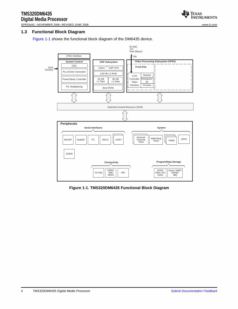
1.3 Functional Block Diagram
JTAG Interface
System Control
PLLs/Clock Generator
InputClock(s)
Power/Sleep Controller
Pin Multiplexing
DSP Subsystem
C64x+ DSP CPU
32 KBL1 Pgm
128 KB L2 RAM
80 KBL1 Data
BT.656, Y/C,Raw (Bayer)
Video Processing Subsystem (VPSS)
CCDController
VideoInterface
Front End
Resizer
Histogram/3A
Preview
Switched Central Resource (SCR)
Peripherals
EDMA
I2C HECC UART
Serial Interfaces
DDR2Mem Ctlr
(32b)
Async EMIF/NAND/
(8b)
Program/Data Storage
WatchdogTimer PWM
System
General-Purpose
Timer
VLYNQEMACWith
MDIO
Connectivity
HPI
McASP McBSP
OSC
Boot ROM
16b
GPIO
TMS320DM6435Digital Media ProcessorSPRS344C–NOVEMBER 2006–REVISED JUNE 2008 www.ti.com
Figure 1-1 shows the functional block diagram of the DM6435 device.
Figure 1-1. TMS320DM6435 Functional Block Diagram
4 TMS320DM6435 Digital Media Processor Submit Documentation Feedback
Contents
TMS320DM6435Digital Media Processor
www.ti.com SPRS344C–NOVEMBER 2006–REVISED JUNE 2008
1 TMS320DM6435 Digital Media Processor........... 1 Temperature (Unless Otherwise Noted) ........... 1271.1 Features .............................................. 1 6 Peripheral Information and Electrical
Specifications ......................................... 1291.2 Description............................................ 26.1 Parameter Information ............................. 1291.3 Functional Block Diagram ............................ 46.2 Recommended Clock and Control Signal TransitionRevision History............................................... 6
Behavior............................................ 1302 Device Overview ......................................... 76.3 Power Supplies .................................... 130
2.1 Device Characteristics................................ 76.4 Enhanced Direct Memory Access (EDMA3)
2.2 CPU (DSP Core) Description......................... 8 Controller........................................... 1372.3 C64x+ CPU.......................................... 11 6.5 Reset............................................... 1492.4 Memory Map Summary ............................. 12 6.6 External Clock Input From MXI/CLKIN Pin ........ 1582.5 Pin Assignments .................................... 16 6.7 Clock PLLs ......................................... 1602.6 Terminal Functions .................................. 24 6.8 Interrupts ........................................... 1652.7 Device Support ...................................... 58 6.9 External Memory Interface (EMIF)................. 1682.8 Device and Development-Support Tool 6.10 Video Processing Sub-System (VPSS) Overview . 176
Nomenclature ....................................... 586.11 Universal Asynchronous Receiver/Transmitter
2.9 Documentation Support ............................. 60 (UART) ............................................. 1873 Device Configuration .................................. 61 6.12 Inter-Integrated Circuit (I2C) ....................... 190
3.1 System Module Registers ........................... 61 6.13 Host-Port Interface (HPI) Peripheral ............... 1943.2 Power Considerations ............................... 62 6.14 Multichannel Buffered Serial Port (McBSP)........ 1993.3 Clock Considerations................................ 64 6.15 Multichannel Audio Serial Port (McASP0)
Peripheral .......................................... 2083.4 Boot Sequence ...................................... 676.16 High-End Controller Area Network Controller3.5 Configurations At Reset ............................. 78
(HECC)............................................. 2163.6 Configurations After Reset .......................... 806.17 Ethernet Media Access Controller (EMAC) ........ 2223.7 Multiplexed Pin Configurations ...................... 846.18 Management Data Input/Output (MDIO) .......... 2293.8 Device Initialization Sequence After Reset ........ 1196.19 Timers.............................................. 2303.9 Debugging Considerations......................... 1216.20 Pulse Width Modulator (PWM)..................... 2334 System Interconnect ................................. 1236.21 VLYNQ ............................................. 2354.1 System Interconnect Block Diagram............... 1236.22 General-Purpose Input/Output (GPIO)............. 2395 Device Operating Conditions....................... 1256.23 IEEE 1149.1 JTAG................................. 2435.1 Absolute Maximum Ratings Over Operating
7 Mechanical Data....................................... 245Temperature Range (Unless Otherwise Noted) ... 1257.1 Thermal Data for ZWT ............................. 2455.2 Recommended Operating Conditions ............. 126
5.3 Electrical Characteristics Over Recommended 7.1.1 Thermal Data for ZDU............................. 246Ranges of Supply Voltage and Operating 7.1.2 Packaging Information............................. 246
Submit Documentation Feedback Contents 5
Revision History
TMS320DM6435Digital Media ProcessorSPRS344C–NOVEMBER 2006–REVISED JUNE 2008 www.ti.com
NOTE: Page numbers for previous revisions may differ from page numbers in the current version.
This data manual revision history highlights the technical changes made to the SPRS344B device-specificdata manual to make it an SPRS344C revision.
This data manual revision history highlights the technical changes made to the SPRS344B device-specificdata manual to make it an SPRS344C revision.
Scope: Applicable updates to the TMS320DM643x DMP, specifically relating to the TMS320DM6435device, have been incorporated.• Added 660- and 700-MHz C64x+™ device speeds.• Added designators for low-power (-L) devices.
SEE ADDITIONS/MODIFICATIONS/DELETIONSGlobal
• Updated/Changed signal name from "C_WE" to "C_WE"• Updated/Changed signal name from "C_WEN" to "C_WE"
Section 1.1 Added "5280, 5600 MIPS" to "High-Performance Digital Signal Processor (DM6435)" bulletSection 1.2 • In first paragraph, updated/changed the following:
– First sentence from "With performance up to 4800 million instructions per second (MIPS) at a clockrate of 600 MHz..." to "With performance up to 5600 million instructions per second (MIPS) with aclock rate of 700 MHz..."
– Fifth sentence from "The DSP core can produce...for a total of 2400 million MACs per second...or atotal of 4800 MMACS."to "The DSP core can produce...for a total of 2800 million MACs persecond...or a total of 5600 MMACS."
Section 2.6 Table 2-19, Multichannel Audio Serial Port (McASP0) Terminal Functions:• Updated/Changed AFSR0/DR0/GP[100] pin description from "... frame synchronization AFSX0..." to
"...frame synchronization AFSR0..."• Updated/Changed AFSX0/DX1/GP[107] pin description from "...frame synchronization AFSR0..." to
"...frame synchronization AFSX0..."Section 2.8 Updated/Changed Figure 2-10, Device Nomenclature, to reflect new device speeds and low-power
designator (-L suffix).Section 5 Added footnote to Section 5.1, Absolute Maximum Ratings Over Operating Temperature Range (Unless
Otherwise Noted).Section 5 Updated/Changed ICDD and IDDD test conditions and footnote in Section 5.3, Electrical Characteristics Over
Recommended Ranges of Supply Voltage and Operating Temperature (Unless Otherwise Noted).Section 5.2 Deleted "Future variants..." footnote from table
Section 6.7.1 Table 6-15, PLLC1 Clock Frequency Ranges:• Updated/Changed PLLOUT 1.2V-CVDD max value from "700 MHz" to "600 MHz" for
-6/-5/-4/-L/-Q6/-Q5/-Q4 devices.• Updated/Changed SYSCLK1 1.05V-CVDD max value from "560 MHz" to "520 MHz" for -7 devices.
Section 6.7.1 Updated/Changed sentence from "TI requires EMI filter manufacturer Murata..." to "TI recommends EMIfilter manufacturer Murata..."
Section 6.7.4 Deleted "(-4, -4Q, -4S, -5, -5Q, -5S, -6)" from Table 6-19 title, Timing Requirements for MXI/CLKIN.
Revision History6 Submit Documentation Feedback
2 Device Overview
2.1 Device Characteristics
TMS320DM6435Digital Media Processor
www.ti.com SPRS344C–NOVEMBER 2006–REVISED JUNE 2008
Table 2-1, provides an overview of the TMS320DM6435 DSP. The tables show significant features of theDM6435 device, including the capacity of on-chip RAM, the peripherals, the CPU frequency, and thepackage type with pin count.
Table 2-1. Characteristics of the DM6435 ProcessorHARDWARE FEATURES DM6435DDR2 Memory Controller (16-/32-bit bus width) [1.8 V I/O]
Asynchronous (8-bit bus width),Asynchronous EMIF [EMIFA] RAM, Flash, (8-bit NOR or 8-bit NAND)EDMA3 1 (64 independent channels, 8 QDMA channels)
2 64-bit General PurposeTimers (configurable as 2 64-bit or 4 32-bit)
1 64-bit Watch DogUARTs 2 (one with RTS and CTS flow control)PeripheralsI2C 1 (Master/Slave)
Not all peripherals pinsMcBSP 1are available at the same
time (For more detail, see McASP 1 (4 serailizers)the Device Configuration
10/100 Ethernet MAC (EMAC) withsection). 1Management Data Input/Output (MDIO)VLYNQ 1General-Purpose Input/Output Port (GPIO) Up to 111 pinsPWM 3 outputsHPI (16-bit) 1Configurable Video Port 1 Input (VPFE)HECC 1Size (Bytes) 240KB RAM, 64KB ROM
32K-Byte (32KB) L1 Program (L1P) RAM/Cache(Cache up to 32KB)On-Chip Memory
Organization 80KB L1 Data (L1D) RAM/Cache (Cache up to 32KB)128KB Unified Mapped RAM/Cache (L2)64KB Boot ROM
Revision ID Register (MM_REVID.[15:0]) See the TMS320DM6437/35/33/31 Digital MediaMegaModule Rev ID (address location: 0x0181 2000) Processor (DMP) [Silicon Revisions 1.1 and 1.0]Silicon Errata (literature number SPRZ250).CPU ID + CPU Rev ID Control Status Register (CSR.[31:16])
JTAGID register See Section 6.23.1, JTAG ID (JTAGID) RegisterJTAG BSDL_ID (address location: 0x01C4 0028) Description(s)700 (-7)
660 (-Q6)CPU Frequency (1) (2) MHz 600 (-6/-L)
500 (-5/-Q5)400 (-4/-Q4)
2.5 ns (-4/-Q4)2 ns (-5/-Q5)
Cycle Time (1) (2) ns 1.67 ns (-6/-L)1.51 ns (-Q6)1.43 ns (-7)
(1) Performance numbers assume core voltage is set to 1.2V.(2) Applies to "tape and reel" part number counterparts as well. For more information, see Section 2.8, Device and Development-Support
Tool Nomenclature.
Submit Documentation Feedback Device Overview 7
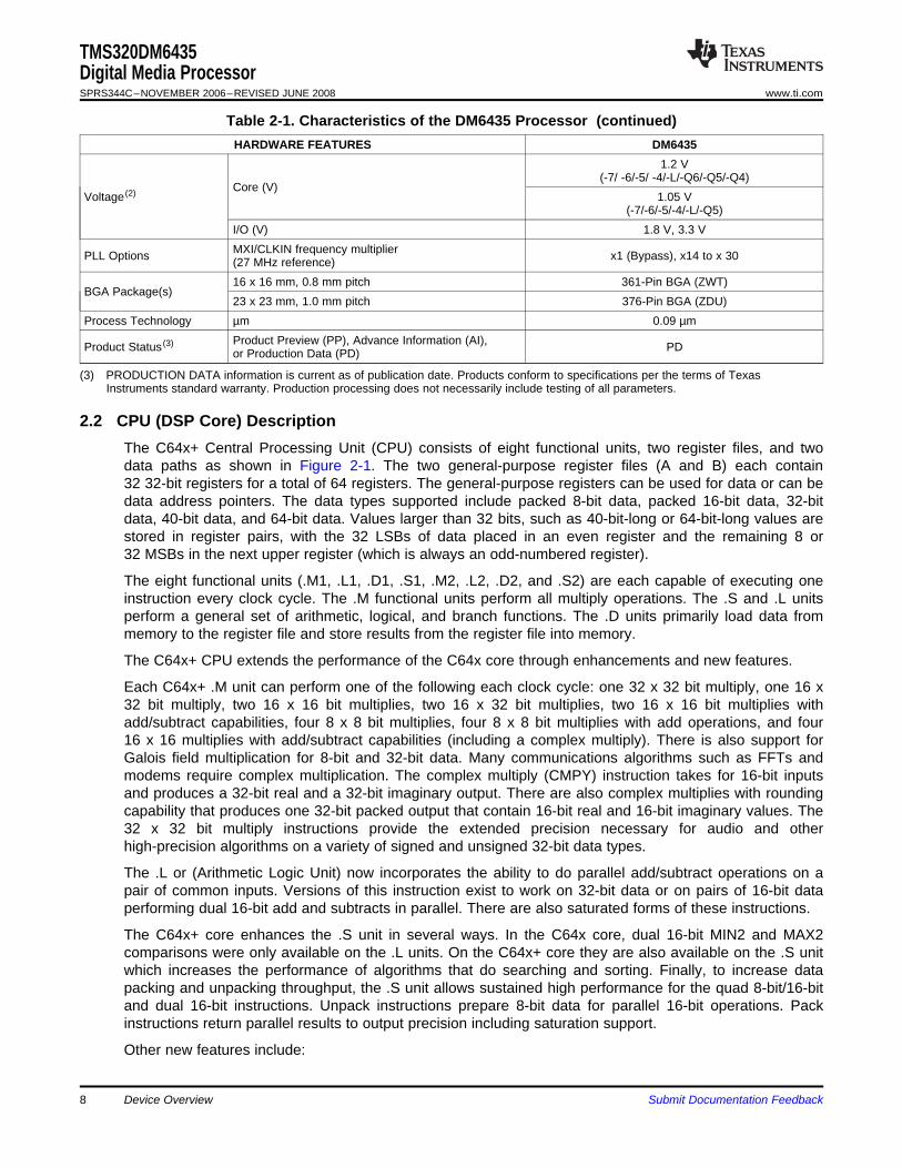
2.2 CPU (DSP Core) Description
TMS320DM6435Digital Media ProcessorSPRS344C–NOVEMBER 2006–REVISED JUNE 2008 www.ti.com
Table 2-1. Characteristics of the DM6435 Processor (continued)HARDWARE FEATURES DM6435
1.2 V(-7/ -6/-5/ -4/-L/-Q6/-Q5/-Q4)
Core (V)Voltage (2) 1.05 V
(-7/-6/-5/-4/-L/-Q5)I/O (V) 1.8 V, 3.3 VMXI/CLKIN frequency multiplierPLL Options x1 (Bypass), x14 to x 30(27 MHz reference)16 x 16 mm, 0.8 mm pitch 361-Pin BGA (ZWT)
BGA Package(s)23 x 23 mm, 1.0 mm pitch 376-Pin BGA (ZDU)
Process Technology µm 0.09 µmProduct Preview (PP), Advance Information (AI),Product Status (3) PDor Production Data (PD)
(3) PRODUCTION DATA information is current as of publication date. Products conform to specifications per the terms of TexasInstruments standard warranty. Production processing does not necessarily include testing of all parameters.
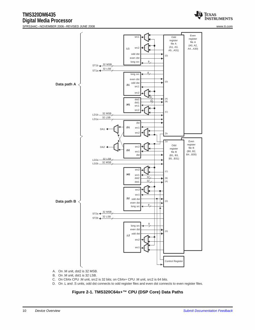
The C64x+ Central Processing Unit (CPU) consists of eight functional units, two register files, and twodata paths as shown in Figure 2-1. The two general-purpose register files (A and B) each contain32 32-bit registers for a total of 64 registers. The general-purpose registers can be used for data or can bedata address pointers. The data types supported include packed 8-bit data, packed 16-bit data, 32-bitdata, 40-bit data, and 64-bit data. Values larger than 32 bits, such as 40-bit-long or 64-bit-long values arestored in register pairs, with the 32 LSBs of data placed in an even register and the remaining 8 or32 MSBs in the next upper register (which is always an odd-numbered register).
The eight functional units (.M1, .L1, .D1, .S1, .M2, .L2, .D2, and .S2) are each capable of executing oneinstruction every clock cycle. The .M functional units perform all multiply operations. The .S and .L unitsperform a general set of arithmetic, logical, and branch functions. The .D units primarily load data frommemory to the register file and store results from the register file into memory.
The C64x+ CPU extends the performance of the C64x core through enhancements and new features.
Each C64x+ .M unit can perform one of the following each clock cycle: one 32 x 32 bit multiply, one 16 x32 bit multiply, two 16 x 16 bit multiplies, two 16 x 32 bit multiplies, two 16 x 16 bit multiplies withadd/subtract capabilities, four 8 x 8 bit multiplies, four 8 x 8 bit multiplies with add operations, and four16 x 16 multiplies with add/subtract capabilities (including a complex multiply). There is also support forGalois field multiplication for 8-bit and 32-bit data. Many communications algorithms such as FFTs andmodems require complex multiplication. The complex multiply (CMPY) instruction takes for 16-bit inputsand produces a 32-bit real and a 32-bit imaginary output. There are also complex multiplies with roundingcapability that produces one 32-bit packed output that contain 16-bit real and 16-bit imaginary values. The32 x 32 bit multiply instructions provide the extended precision necessary for audio and otherhigh-precision algorithms on a variety of signed and unsigned 32-bit data types.
The .L or (Arithmetic Logic Unit) now incorporates the ability to do parallel add/subtract operations on apair of common inputs. Versions of this instruction exist to work on 32-bit data or on pairs of 16-bit dataperforming dual 16-bit add and subtracts in parallel. There are also saturated forms of these instructions.
The C64x+ core enhances the .S unit in several ways. In the C64x core, dual 16-bit MIN2 and MAX2comparisons were only available on the .L units. On the C64x+ core they are also available on the .S unitwhich increases the performance of algorithms that do searching and sorting. Finally, to increase datapacking and unpacking throughput, the .S unit allows sustained high performance for the quad 8-bit/16-bitand dual 16-bit instructions. Unpack instructions prepare 8-bit data for parallel 16-bit operations. Packinstructions return parallel results to output precision including saturation support.
Other new features include:
Device Overview8 Submit Documentation Feedback
TMS320DM6435Digital Media Processor
www.ti.com SPRS344C–NOVEMBER 2006–REVISED JUNE 2008
• SPLOOP - A small instruction buffer in the CPU that aids in creation of software pipelining loops wheremultiple iterations of a loop are executed in parallel. The SPLOOP buffer reduces the code sizeassociated with software pipelining. Furthermore, loops in the SPLOOP buffer are fully interruptible.
• Compact Instructions - The native instruction size for the C6000 devices is 32 bits. Many commoninstructions such as MPY, AND, OR, ADD, and SUB can be expressed as 16 bits if the C64x+compiler can restrict the code to use certain registers in the register file. This compression isperformed by the code generation tools.
• Instruction Set Enhancement - As noted above, there are new instructions such as 32-bitmultiplications, complex multiplications, packing, sorting, bit manipulation, and 32-bit Galois fieldmultiplication.
• Exceptions Handling - Intended to aid the programmer in isolating bugs. The C64x+ CPU is able todetect and respond to exceptions, both from internally detected sources (such as illegal op-codes) andfrom system events (such as a watchdog time expiration).
• Privilege - Defines user and supervisor modes of operation, allowing the operating system to give abasic level of protection to sensitive resources. Local memory is divided into multiple pages, each withread, write, and execute permissions.
• Time-Stamp Counter - Primarily targeted for Real-Time Operating System (RTOS) robustness, afree-running time-stamp counter is implemented in the CPU which is not sensitive to system stalls.
For more details on the C64x+ CPU and its enhancements over the C64x architecture, see the followingdocuments:• TMS320C64x/C64x+ DSP CPU and Instruction Set Reference Guide (literature number SPRU732)• TMS320C64x+ DSP Megamodule Reference Guide (literature number SPRU871)• TMS320C64x to TMS320C64x+ CPU Migration Guide Application Report (literature number SPRAA84)• TMS320C64x+ DSP Cache User's Guide (literature number SPRU862)
Submit Documentation Feedback Device Overview 9
src2
src2
ÁÁÁÁÁÁÁ .D1
.M1 ÁÁÁÁÁÁÁÁÁÁ ÁÁÁ.S1
ÁÁÁÁÁÁÁ ÁÁÁ.L1
long src
odd dst
src2
src1 ÁÁÁÁÁÁÁÁÁÁÁÁÁÁÁÁÁÁÁÁÁsrc1
src1
src1
even dst
even dst
odd dst
dst1
dst
src2
src2
src2
long src
DA1
ST1b
LD1b
LD1a
ST1a
Data path A
Oddregister
file A(A1, A3,
A5...A31)ÁÁÁOdd
registerfile B
(B1, B3,B5...B31)
ÁÁÁ.D2
ÁÁÁÁsrc1dst
src2DA2
LD2aLD2b
src2
.M2 src1
ÁÁÁdst1
ÁÁÁ.S2
src1
ÁÁÁÁeven dstlong src
odd dst
ST2a
ST2b
long src
.L2
ÁÁÁÁeven dst
odd dst
ÁÁÁsrc1
Data path B
Control Register
32 MSB
32 LSB
dst2 (A)
32 MSB
32 LSB
2x
1x
32 LSB32 MSB
32 LSB
32 MSB
dst2
(B)
(B)
(A)
8
8
8
8
32
32
3232
(C)
(C)
Evenregister
file A(A0, A2,
A4...A30)
Evenregister
file B(B0, B2,
B4...B30)
(D)
(D)
(D)
(D)
A. On .M unit, dst2 is 32 MSB.B. On .M unit, dst1 is 32 LSB.C. On C64x CPU .M unit, src2 is 32 bits; on C64x+ CPU .M unit, src2 is 64 bits.D. On .L and .S units, odd dst connects to odd register files and even dst connects to even register files.
TMS320DM6435Digital Media ProcessorSPRS344C–NOVEMBER 2006–REVISED JUNE 2008 www.ti.com
Figure 2-1. TMS320C64x+™ CPU (DSP Core) Data Paths
10 Device Overview Submit Documentation Feedback
2.3 C64x+ CPU
TMS320DM6435Digital Media Processor
www.ti.com SPRS344C–NOVEMBER 2006–REVISED JUNE 2008
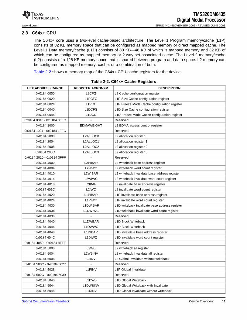
The C64x+ core uses a two-level cache-based architecture. The Level 1 Program memory/cache (L1P)consists of 32 KB memory space that can be configured as mapped memory or direct mapped cache. TheLevel 1 Data memory/cache (L1D) consists of 80 KB—48 KB of which is mapped memory and 32 KB ofwhich can be configured as mapped memory or 2-way set associated cache. The Level 2 memory/cache(L2) consists of a 128 KB memory space that is shared between program and data space. L2 memory canbe configured as mapped memory, cache, or a combination of both.
Table 2-2 shows a memory map of the C64x+ CPU cache registers for the device.
Table 2-2. C64x+ Cache RegistersHEX ADDRESS RANGE REGISTER ACRONYM DESCRIPTION
0x0184 0000 L2CFG L2 Cache configuration register0x0184 0020 L1PCFG L1P Size Cache configuration register0x0184 0024 L1PCC L1P Freeze Mode Cache configuration register0x0184 0040 L1DCFG L1D Size Cache configuration register0x0184 0044 L1DCC L1D Freeze Mode Cache configuration register
0x0184 0048 - 0x0184 0FFC - Reserved0x0184 1000 EDMAWEIGHT L2 EDMA access control register
0x0184 1004 - 0x0184 1FFC - Reserved0x0184 2000 L2ALLOC0 L2 allocation register 00x0184 2004 L2ALLOC1 L2 allocation register 10x0184 2008 L2ALLOC2 L2 allocation register 20x0184 200C L2ALLOC3 L2 allocation register 3
0x0184 2010 - 0x0184 3FFF - Reserved0x0184 4000 L2WBAR L2 writeback base address register0x0184 4004 L2WWC L2 writeback word count register0x0184 4010 L2WIBAR L2 writeback invalidate base address register0x0184 4014 L2WIWC L2 writeback invalidate word count register0x0184 4018 L2IBAR L2 invalidate base address register0x0184 401C L2IWC L2 invalidate word count register0x0184 4020 L1PIBAR L1P invalidate base address register0x0184 4024 L1PIWC L1P invalidate word count register0x0184 4030 L1DWIBAR L1D writeback invalidate base address register0x0184 4034 L1DWIWC L1D writeback invalidate word count register0x0184 4038 - Reserved0x0184 4040 L1DWBAR L1D Block Writeback0x0184 4044 L1DWWC L1D Block Writeback0x0184 4048 L1DIBAR L1D invalidate base address register0x0184 404C L1DIWC L1D invalidate word count register
0x0184 4050 - 0x0184 4FFF - Reserved0x0184 5000 L2WB L2 writeback all register0x0184 5004 L2WBINV L2 writeback invalidate all register0x0184 5008 L2INV L2 Global Invalidate without writeback
0x0184 500C - 0x0184 5027 - Reserved0x0184 5028 L1PINV L1P Global Invalidate
0x0184 502C - 0x0184 5039 - Reserved0x0184 5040 L1DWB L1D Global Writeback0x0184 5044 L1DWBINV L1D Global Writeback with Invalidate0x0184 5048 L1DINV L1D Global Invalidate without writeback
Submit Documentation Feedback Device Overview 11
2.4 Memory Map Summary
TMS320DM6435Digital Media ProcessorSPRS344C–NOVEMBER 2006–REVISED JUNE 2008 www.ti.com
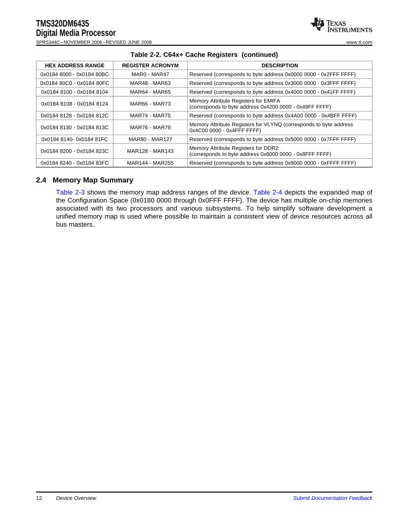
Table 2-2. C64x+ Cache Registers (continued)HEX ADDRESS RANGE REGISTER ACRONYM DESCRIPTION
0x0184 8000 - 0x0184 80BC MAR0 - MAR47 Reserved (corresponds to byte address 0x0000 0000 - 0x2FFF FFFF)0x0184 80C0 - 0x0184 80FC MAR48 - MAR63 Reserved (corresponds to byte address 0x3000 0000 - 0x3FFF FFFF)0x0184 8100 - 0x0184 8104 MAR64 - MAR65 Reserved (corresponds to byte address 0x4000 0000 - 0x41FF FFFF)
Memory Attribute Registers for EMIFA0x0184 8108 - 0x0184 8124 MAR66 - MAR73 (corresponds to byte address 0x4200 0000 - 0x49FF FFFF)0x0184 8128 - 0x0184 812C MAR74 - MAR75 Reserved (corresponds to byte address 0x4A00 0000 - 0x4BFF FFFF)
Memory Attribute Registers for VLYNQ (corresponds to byte address0x0184 8130 - 0x0184 813C MAR76 - MAR79 0x4C00 0000 - 0x4FFF FFFF)0x0184 8140- 0x0184 81FC MAR80 - MAR127 Reserved (corresponds to byte address 0x5000 0000 - 0x7FFF FFFF)
Memory Attribute Registers for DDR20x0184 8200 - 0x0184 823C MAR128 - MAR143 (corresponds to byte address 0x8000 0000 - 0x8FFF FFFF)0x0184 8240 - 0x0184 83FC MAR144 - MAR255 Reserved (corresponds to byte address 0x9000 0000 - 0xFFFF FFFF)
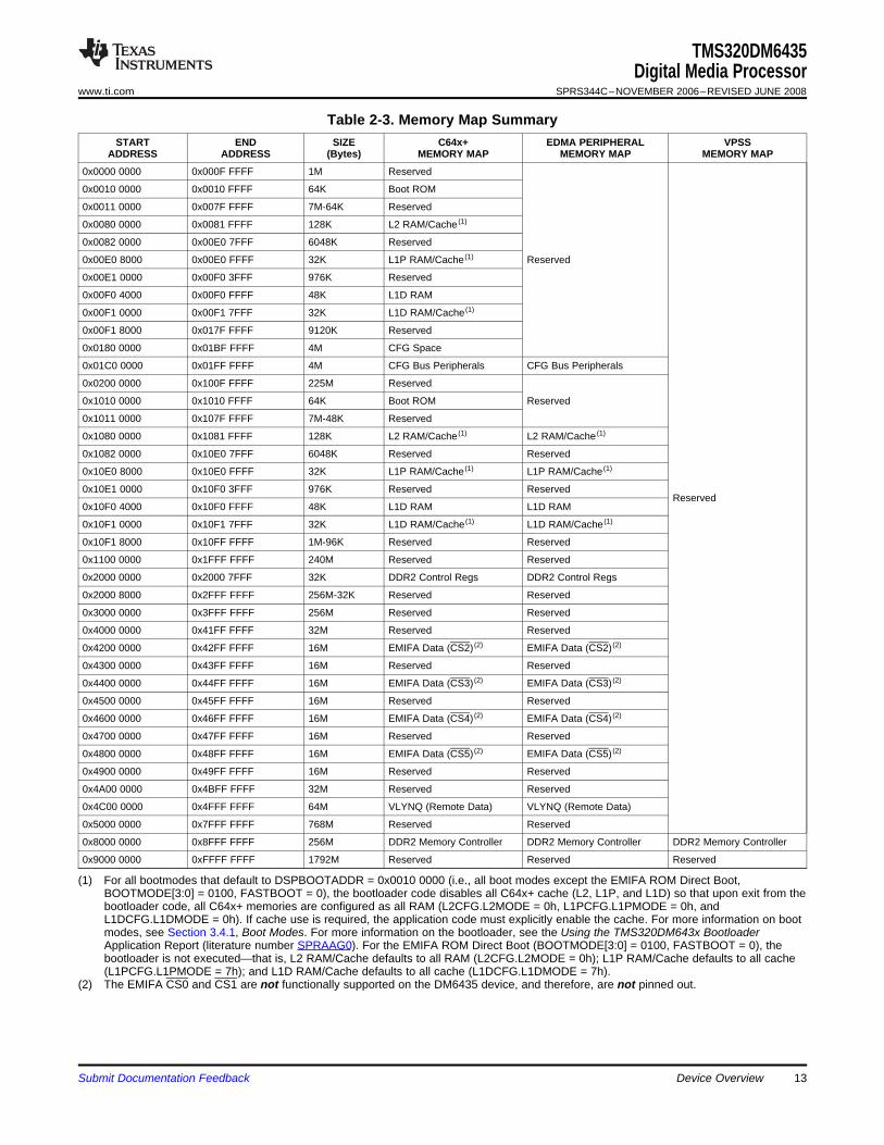
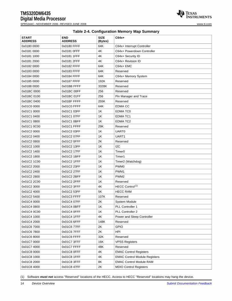
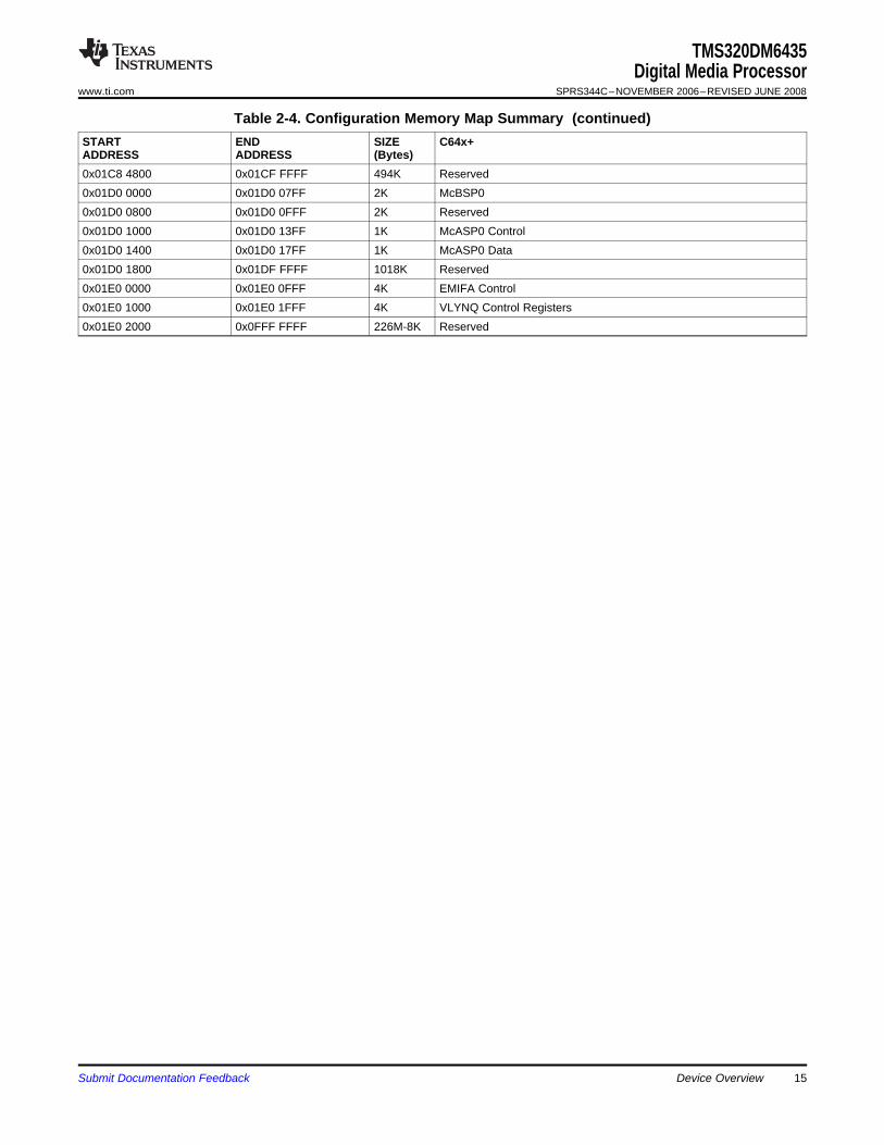
Table 2-3 shows the memory map address ranges of the device. Table 2-4 depicts the expanded map ofthe Configuration Space (0x0180 0000 through 0x0FFF FFFF). The device has multiple on-chip memoriesassociated with its two processors and various subsystems. To help simplify software development aunified memory map is used where possible to maintain a consistent view of device resources across allbus masters.
12 Device Overview Submit Documentation Feedback
TMS320DM6435Digital Media Processor
www.ti.com SPRS344C–NOVEMBER 2006–REVISED JUNE 2008
Table 2-3. Memory Map SummarySTART END SIZE C64x+ EDMA PERIPHERAL VPSS
ADDRESS ADDRESS (Bytes) MEMORY MAP MEMORY MAP MEMORY MAP
0x0000 0000 0x000F FFFF 1M Reserved
0x0010 0000 0x0010 FFFF 64K Boot ROM
0x0011 0000 0x007F FFFF 7M-64K Reserved
0x0080 0000 0x0081 FFFF 128K L2 RAM/Cache (1)
0x0082 0000 0x00E0 7FFF 6048K Reserved
0x00E0 8000 0x00E0 FFFF 32K L1P RAM/Cache (1) Reserved
0x00E1 0000 0x00F0 3FFF 976K Reserved
0x00F0 4000 0x00F0 FFFF 48K L1D RAM
0x00F1 0000 0x00F1 7FFF 32K L1D RAM/Cache (1)
0x00F1 8000 0x017F FFFF 9120K Reserved
0x0180 0000 0x01BF FFFF 4M CFG Space
0x01C0 0000 0x01FF FFFF 4M CFG Bus Peripherals CFG Bus Peripherals
0x0200 0000 0x100F FFFF 225M Reserved
0x1010 0000 0x1010 FFFF 64K Boot ROM Reserved
0x1011 0000 0x107F FFFF 7M-48K Reserved
0x1080 0000 0x1081 FFFF 128K L2 RAM/Cache (1) L2 RAM/Cache (1)
0x1082 0000 0x10E0 7FFF 6048K Reserved Reserved
0x10E0 8000 0x10E0 FFFF 32K L1P RAM/Cache (1) L1P RAM/Cache (1)
0x10E1 0000 0x10F0 3FFF 976K Reserved ReservedReserved
0x10F0 4000 0x10F0 FFFF 48K L1D RAM L1D RAM
0x10F1 0000 0x10F1 7FFF 32K L1D RAM/Cache (1) L1D RAM/Cache (1)
0x10F1 8000 0x10FF FFFF 1M-96K Reserved Reserved
0x1100 0000 0x1FFF FFFF 240M Reserved Reserved
0x2000 0000 0x2000 7FFF 32K DDR2 Control Regs DDR2 Control Regs
0x2000 8000 0x2FFF FFFF 256M-32K Reserved Reserved
0x3000 0000 0x3FFF FFFF 256M Reserved Reserved
0x4000 0000 0x41FF FFFF 32M Reserved Reserved
0x4200 0000 0x42FF FFFF 16M EMIFA Data (CS2) (2) EMIFA Data (CS2) (2)
0x4300 0000 0x43FF FFFF 16M Reserved Reserved
0x4400 0000 0x44FF FFFF 16M EMIFA Data (CS3) (2) EMIFA Data (CS3) (2)
0x4500 0000 0x45FF FFFF 16M Reserved Reserved
0x4600 0000 0x46FF FFFF 16M EMIFA Data (CS4) (2) EMIFA Data (CS4) (2)
0x4700 0000 0x47FF FFFF 16M Reserved Reserved
0x4800 0000 0x48FF FFFF 16M EMIFA Data (CS5) (2) EMIFA Data (CS5) (2)
0x4900 0000 0x49FF FFFF 16M Reserved Reserved
0x4A00 0000 0x4BFF FFFF 32M Reserved Reserved
0x4C00 0000 0x4FFF FFFF 64M VLYNQ (Remote Data) VLYNQ (Remote Data)
0x5000 0000 0x7FFF FFFF 768M Reserved Reserved
0x8000 0000 0x8FFF FFFF 256M DDR2 Memory Controller DDR2 Memory Controller DDR2 Memory Controller
0x9000 0000 0xFFFF FFFF 1792M Reserved Reserved Reserved
(1) For all bootmodes that default to DSPBOOTADDR = 0x0010 0000 (i.e., all boot modes except the EMIFA ROM Direct Boot,BOOTMODE[3:0] = 0100, FASTBOOT = 0), the bootloader code disables all C64x+ cache (L2, L1P, and L1D) so that upon exit from thebootloader code, all C64x+ memories are configured as all RAM (L2CFG.L2MODE = 0h, L1PCFG.L1PMODE = 0h, andL1DCFG.L1DMODE = 0h). If cache use is required, the application code must explicitly enable the cache. For more information on bootmodes, see Section 3.4.1, Boot Modes. For more information on the bootloader, see the Using the TMS320DM643x BootloaderApplication Report (literature number SPRAAG0). For the EMIFA ROM Direct Boot (BOOTMODE[3:0] = 0100, FASTBOOT = 0), thebootloader is not executed—that is, L2 RAM/Cache defaults to all RAM (L2CFG.L2MODE = 0h); L1P RAM/Cache defaults to all cache(L1PCFG.L1PMODE = 7h); and L1D RAM/Cache defaults to all cache (L1DCFG.L1DMODE = 7h).
(2) The EMIFA CS0 and CS1 are not functionally supported on the DM6435 device, and therefore, are not pinned out.
Submit Documentation Feedback Device Overview 13
TMS320DM6435Digital Media ProcessorSPRS344C–NOVEMBER 2006–REVISED JUNE 2008 www.ti.com
Table 2-4. Configuration Memory Map SummarySTART END SIZE C64x+ADDRESS ADDRESS (Bytes)0x0180 0000 0x0180 FFFF 64K C64x+ Interrupt Controller0x0181 0000 0x0181 0FFF 4K C64x+ Powerdown Controller0x0181 1000 0x0181 1FFF 4K C64x+ Security ID0x0181 2000 0x0181 2FFF 4K C64x+ Revision ID0x0182 0000 0x0182 FFFF 64K C64x+ EMC0x0183 0000 0x0183 FFFF 64K Reserved0x0184 0000 0x0184 FFFF 64K C64x+ Memory System0x0185 0000 0x0187 FFFF 192K Reserved0x0188 0000 0x01BB FFFF 3328K Reserved0x01BC 0000 0x01BC 00FF 256 Reserved0x01BC 0100 0x01BC 01FF 256 Pin Manager and Trace0x01BC 0400 0x01BF FFFF 255K Reserved0x01C0 0000 0x01C0 FFFF 64K EDMA CC0x01C1 0000 0x01C1 03FF 1K EDMA TC00x01C1 0400 0x01C1 07FF 1K EDMA TC10x01C1 0800 0x01C1 0BFF 1K EDMA TC20x01C1 0C00 0x01C1 FFFF 29K Reserved0x01C2 0000 0x01C2 03FF 1K UART00x01C2 0400 0x01C2 07FF 1K UART10x01C2 0800 0x01C2 0FFF 2K Reserved0x01C2 1000 0x01C2 13FF 1K I2C0x01C2 1400 0x01C2 17FF 1K Timer00x01C2 1800 0x01C2 1BFF 1K Timer10x01C2 1C00 0x01C2 1FFF 1K Timer2 (Watchdog)0x01C2 2000 0x01C2 23FF 1K PWM00x01C2 2400 0x01C2 27FF 1K PWM10x01C2 2800 0x01C2 2BFF 1K PWM20x01C2 2C00 0x01C2 2FFF 1K Reserved0x01C2 3000 0x01C2 3FFF 4K HECC Control (1)
0x01C2 4000 0x01C2 53FF 5K HECC RAM0x01C2 5400 0x01C3 FFFF 107K Reserved0x01C4 0000 0x01C4 07FF 2K System Module0x01C4 0800 0x01C4 0BFF 1K PLL Controller 10x01C4 0C00 0x01C4 0FFF 1K PLL Controller 20x01C4 1000 0x01C4 1FFF 4K Power and Sleep Controller0x01C4 2000 0x01C6 6FFF 148K Reserved0x01C6 7000 0x01C6 77FF 2K GPIO0x01C6 7800 0x01C6 7FFF 2K HPI0x01C6 8000 0x01C6 FFFF 32K Reserved0x01C7 0000 0x01C7 3FFF 16K VPSS Registers0x01C7 4000 0x01C7 FFFF 48K Reserved0x01C8 0000 0x01C8 0FFF 4K EMAC Control Registers0x01C8 1000 0x01C8 1FFF 4K EMAC Control Module Registers0x01C8 2000 0x01C8 3FFF 8K EMAC Control Module RAM0x01C8 4000 0x01C8 47FF 2K MDIO Control Registers
(1) Software must not access "Reserved" locations of the HECC. Access to HECC "Reserved" locations may hang the device.
Device Overview14 Submit Documentation Feedback
TMS320DM6435Digital Media Processor
www.ti.com SPRS344C–NOVEMBER 2006–REVISED JUNE 2008
Table 2-4. Configuration Memory Map Summary (continued)START END SIZE C64x+ADDRESS ADDRESS (Bytes)0x01C8 4800 0x01CF FFFF 494K Reserved0x01D0 0000 0x01D0 07FF 2K McBSP00x01D0 0800 0x01D0 0FFF 2K Reserved0x01D0 1000 0x01D0 13FF 1K McASP0 Control0x01D0 1400 0x01D0 17FF 1K McASP0 Data0x01D0 1800 0x01DF FFFF 1018K Reserved0x01E0 0000 0x01E0 0FFF 4K EMIFA Control0x01E0 1000 0x01E0 1FFF 4K VLYNQ Control Registers0x01E0 2000 0x0FFF FFFF 226M-8K Reserved
Submit Documentation Feedback Device Overview 15
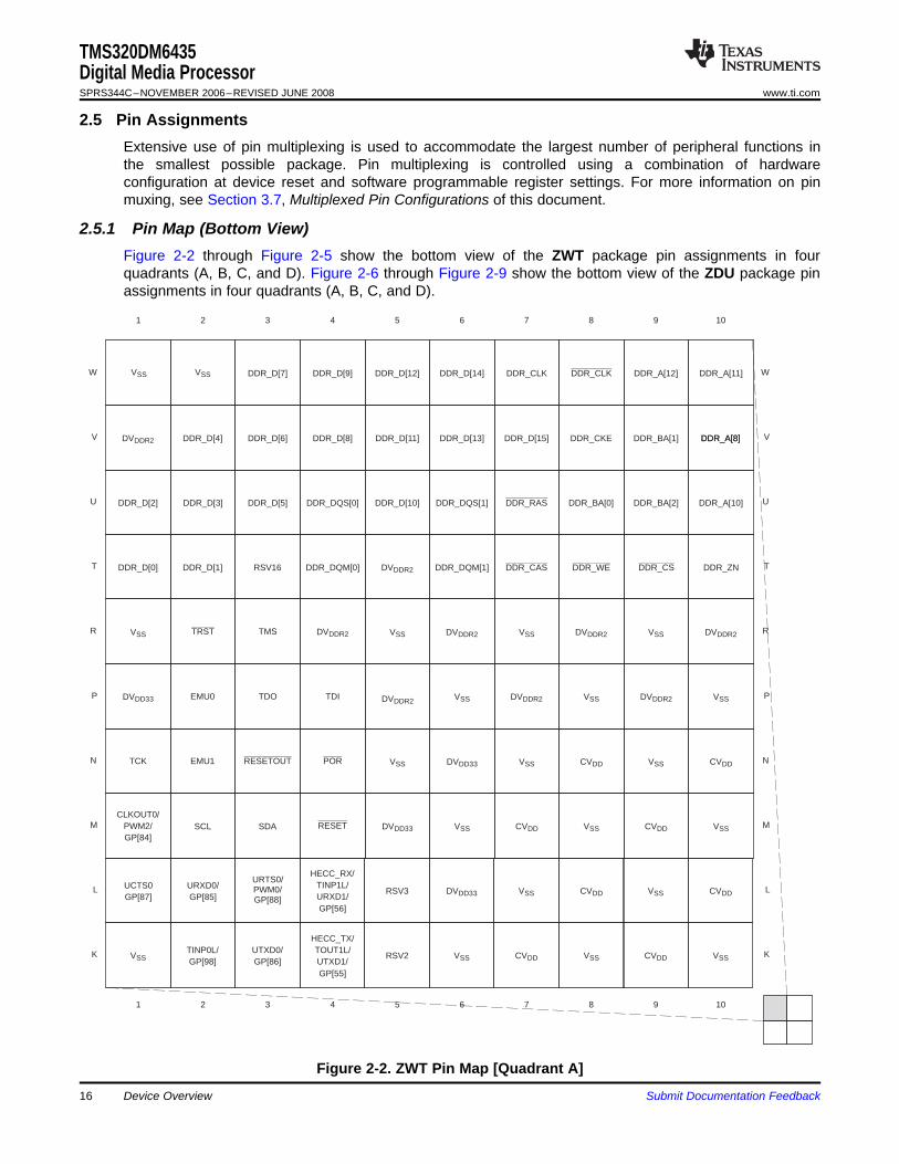
2.5 Pin Assignments
2.5.1 Pin Map (Bottom View)
W
V
U
T
R
P
N
M
L
K
10987654321
10987654321
DDR_D[3]
VSS
HECC_TX/TOUT1L/UTXD1/GP[55]
VSS
UCTS0GP[87]
UTXD0/GP[86]
URXD0/GP[85]
SCL SDA
TCK RESETOUTEMU1 POR
DVDD33 TDOEMU0
TRST DVDDR2TMS
DDR_D[1] DDR_DQM[0]
DDR_D[2]
RSV16
TDI
RESET
RSV3
HECC_RX/TINP1L/URXD1/GP[56]
RSV2
CVDD VSS
VSS
VSS CVDD
DVDDR2
DDR_A[11]DDR_A[12]DDR_CLKDDR_CLKDDR_D[14]
VSS
DVDD33
VSS
DDR_D[5]
DDR_D[6]
DDR_D[9]
VSS
VSS
DVDDR2
DDR_BA[2]
VSS
DDR_D[11] DDR_D[15] DDR_CKE
CVDD
VSS
CVDD
CVDD
VSS
DDR_DQM[1] DDR_CAS DDR_WE DDR_ZN
VSS VSS
DDR_DQS[1] DDR_RAS DDR_A[10]
CVDD CVDD
DVDDR2 DDR_D[4] DDR_D[8] DDR_D[13] DDR_BA[1]
DDR_D[12]
DVDDR2
TINP0L/GP[98]
VSS
VSS
VSS
DVDDR2
CLKOUT0/PWM2/GP[84]
DVDD33 VSS
DVDD33
DVDDR2 DVDDR2
VSS DVDDR2
DDR_CS
CVDD
DDR_DQS[0] DDR_D[10] DDR_BA[0]
DDR_D[0]
URTS0/PWM0/GP[88]
DDR_D[7] W
V
U
T
R
P
N
M
L
K
VSSVSS
DDR_A[8]DDR_A[8]
TMS320DM6435Digital Media ProcessorSPRS344C–NOVEMBER 2006–REVISED JUNE 2008 www.ti.com
Extensive use of pin multiplexing is used to accommodate the largest number of peripheral functions inthe smallest possible package. Pin multiplexing is controlled using a combination of hardwareconfiguration at device reset and software programmable register settings. For more information on pinmuxing, see Section 3.7, Multiplexed Pin Configurations of this document.
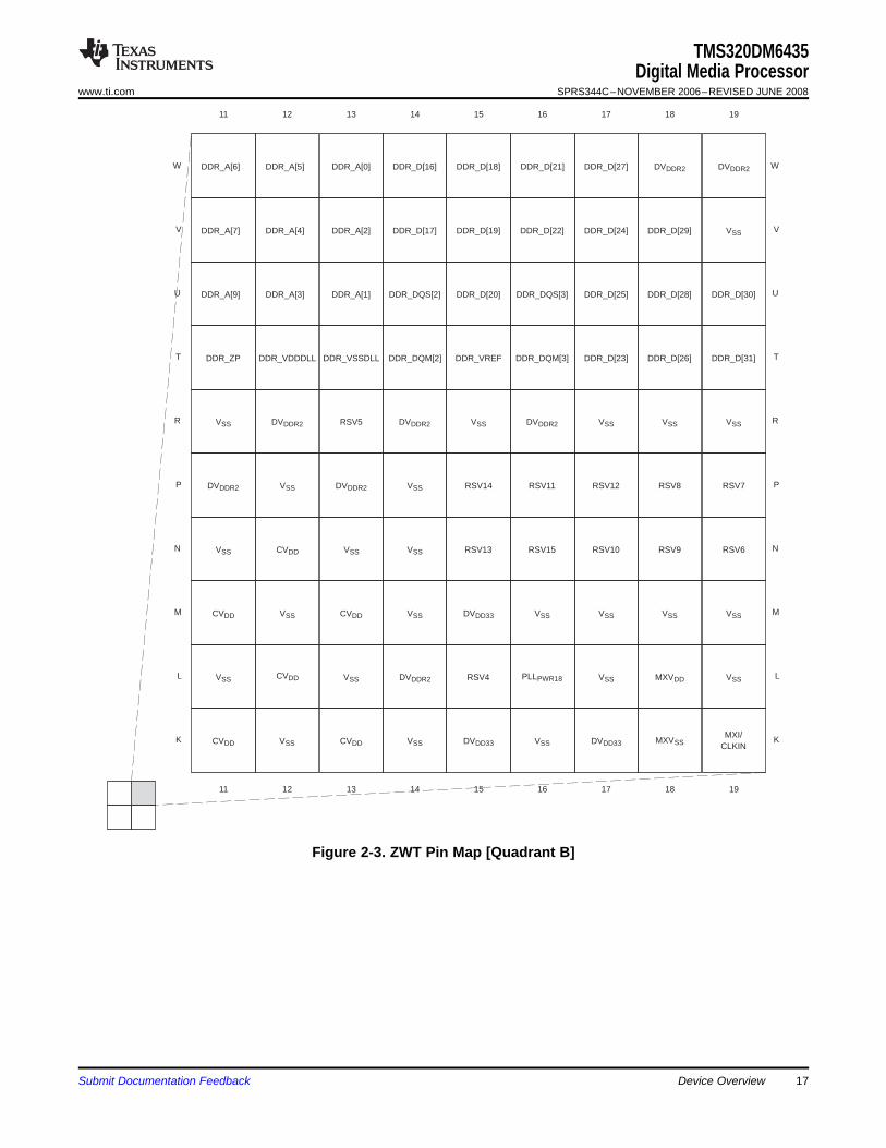
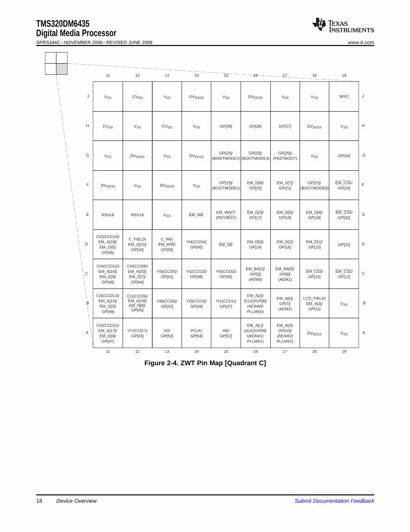
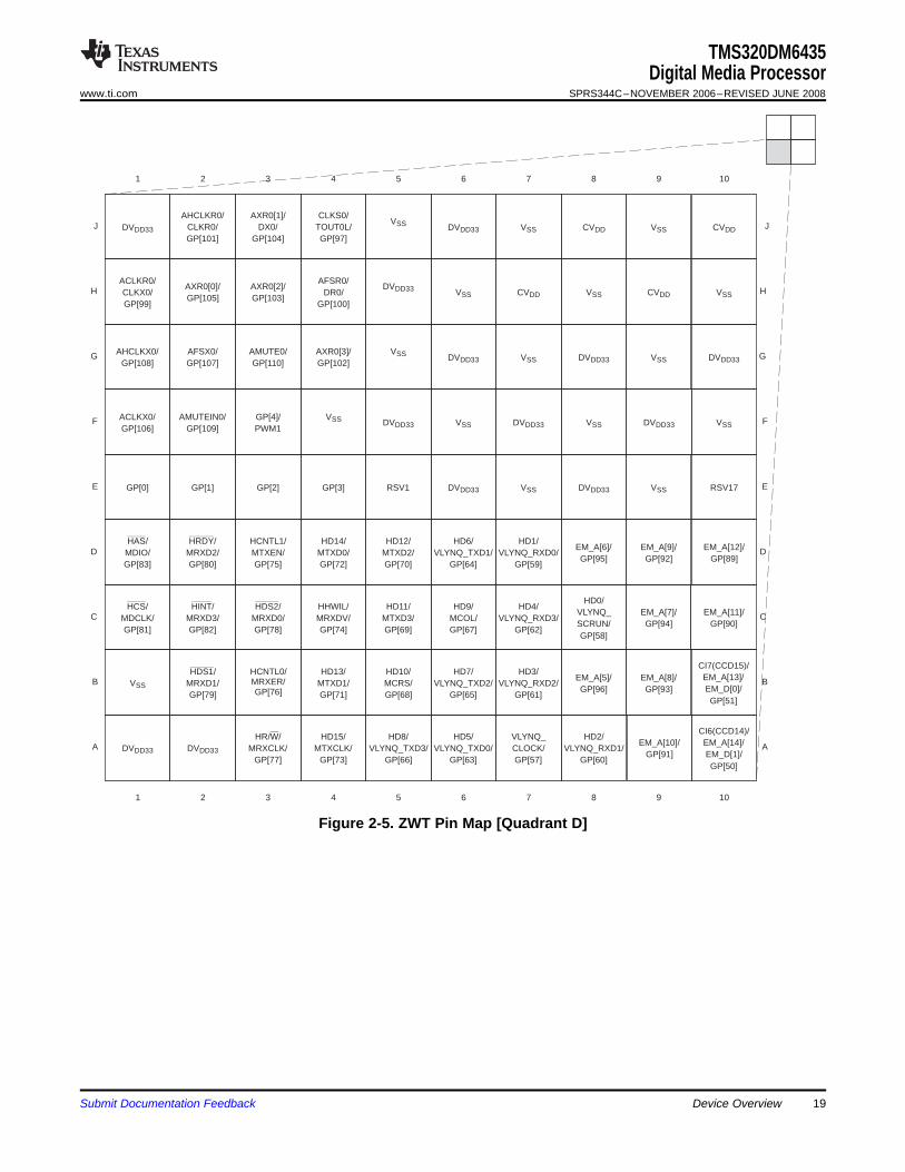
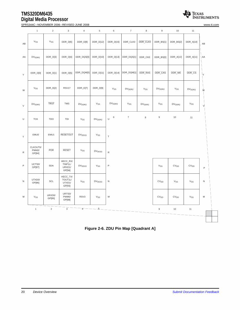
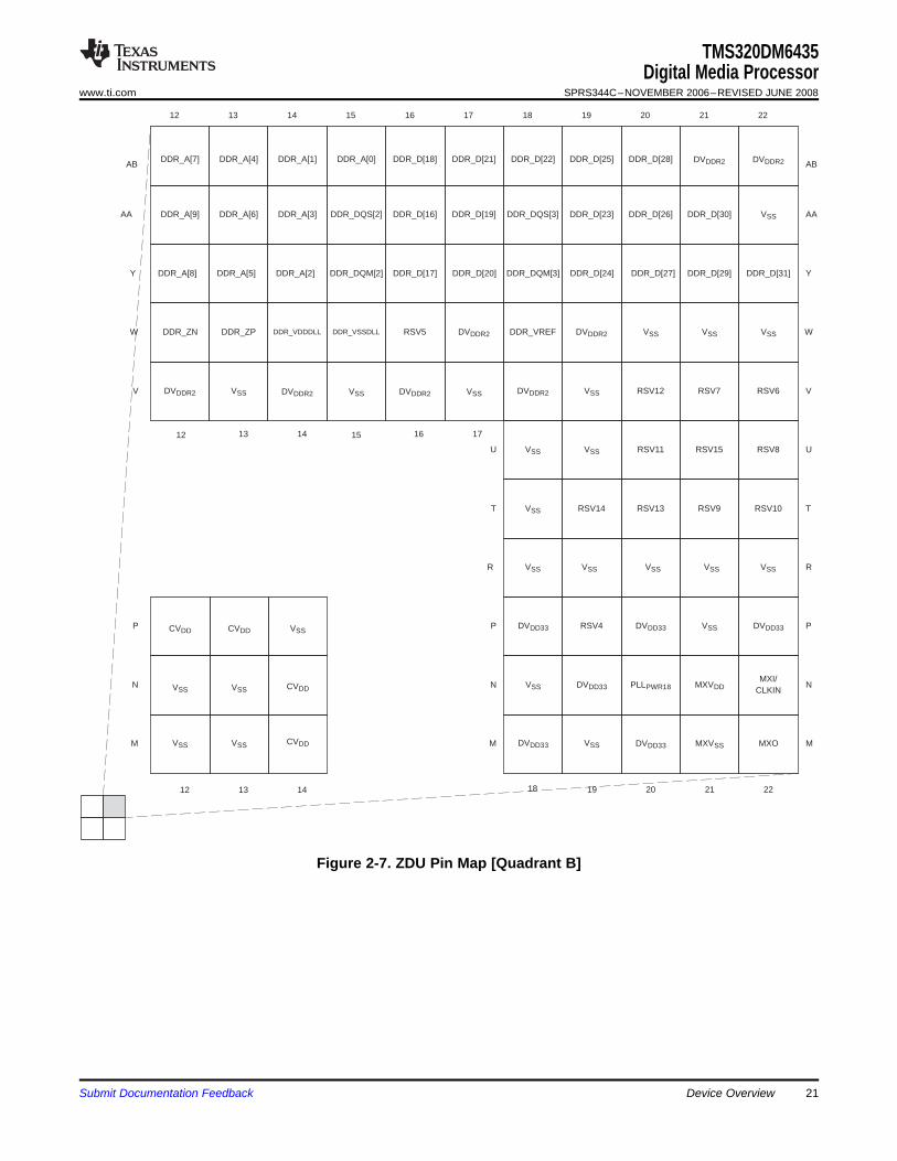
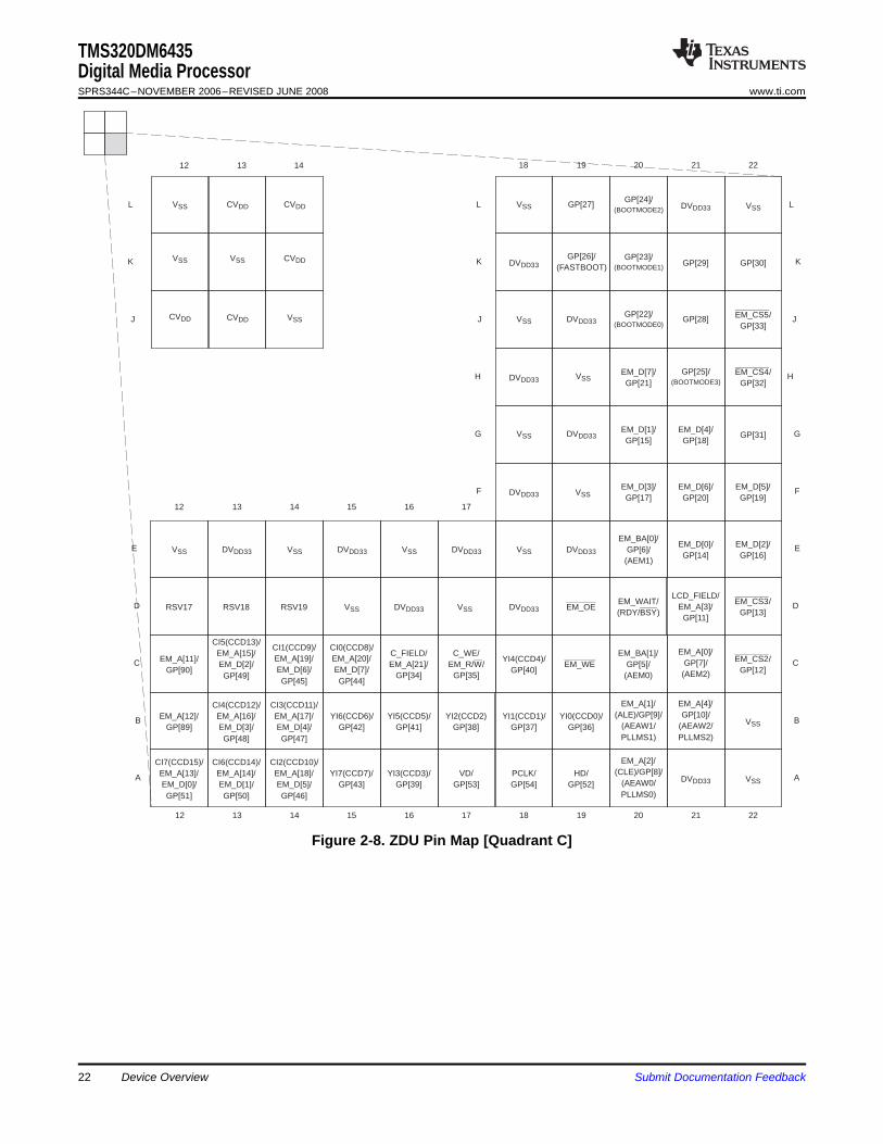
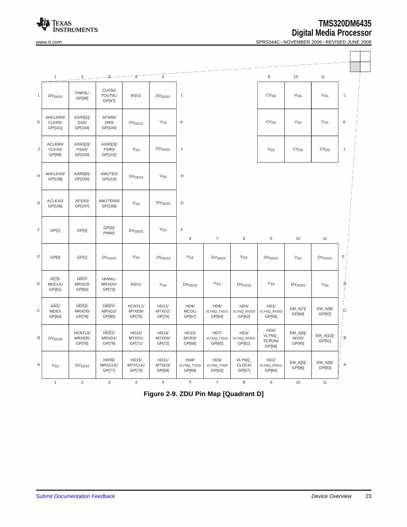
Figure 2-2 through Figure 2-5 show the bottom view of the ZWT package pin assignments in fourquadrants (A, B, C, and D). Figure 2-6 through Figure 2-9 show the bottom view of the ZDU package pinassignments in four quadrants (A, B, C, and D).
Figure 2-2. ZWT Pin Map [Quadrant A]
Device Overview16 Submit Documentation Feedback
W
V
U
T
R
P
N
M
L
K
191817161514131211
191817161514131211
RSV14
CVDDVSS
VSS
CVDD VSS
CVDDVSS VSS
VSSDVDDR2
VSS RSV5DVDDR2
DDR_ZP DDR_VSSDLLDDR_VDDDLL
DVDDR2
CVDD
DVDDR2VSS
VSS
VSS VSS
VSS
RSV9 RSV6
RSV8
DVDDR2DVDDR2DDR_D[27]DDR_D[21]DDR_D[18]
RSV7
RSV4
DVDDR2
VSS
DVDDR2
DDR_DQS[2] DDR_D[28]
MXVDD
DDR_D[17] DDR_D[22] DDR_D[24] VSS
VSS
RSV12
RSV10
VSS
RSV15
DDR_VREF DDR_DQM[3] DDR_D[23] DDR_D[31]
DVDD33MXI/
CLKIN
DDR_D[20] DDR_DQS[3] DDR_D[30]
VSS VSS
DDR_D[19] DDR_D[29]
DDR_D[16]
VSS
CVDD DVDD33
VSS
PLLPWR18
VSS
VSS DVDD33
RSV13
VSS RSV11
VSS
DDR_D[26]
MXVSS
DDR_DQM[2]
DDR_D[25]
CVDD
W
V
U
T
R
P
N
M
L
K
DDR_A[0]
DDR_A[1]
DDR_A[2]
DDR_A[5]
DDR_A[3]
DDR_A[4]
DDR_A[6]
DDR_A[9]
DDR_A[7]
TMS320DM6435Digital Media Processor
www.ti.com SPRS344C–NOVEMBER 2006–REVISED JUNE 2008
Figure 2-3. ZWT Pin Map [Quadrant B]
Submit Documentation Feedback Device Overview 17
H
G
F
E
D
C
B
A
191817161514131211
191817161514131211
CVDD
EM_WAIT/(RDY/BSY)
VD/GP[53]
YI7(CCD7)/GP[43]
CI5(CCD13)/EM_A[15]/EM_D[2]/
GP[49]
CI4(CCD12)/EM_A[16]/EM_D[3]/
GP[48]
CI0(CCD8)/EM_A[20]/EM_D[7]/GP[44]
C_FIELD/EM_A[21]/
GP[34]
CI2(CCD10)/EM_A[18]/EM_D[5]/GP[46]
C_WE/EM_R/W/
GP[35]
RSV19RSV18
DVDD33 DVDD33VSS
VSS VSSDVDD33
VSS
YI5(CCD5)/GP[41]
YI3(CCD3)/GP[39]
YI6(CCD6)/GP[42]
PCLK/GP[54]
EM_CS3/GP[13]
EM_CS2/GP[12]
GP[22]/(BOOTMODE0)
EM_D[1]/GP[15]
GP[31]
EM_D[4]/GP[18]
EM_CS4/GP[32]
YI1(CCD1)/GP[37]
EM_D[6]/GP[20]
VSS
YI4(CCD4)/GP[40]
VSS
DVDD33
DVDD33
LCD_FIELD/EM_A[3]/
GP[11]
EM_A[1]/(ALE)/GP[9]/
(AEAW1/PLLMS1)
EM_D[5]/GP[19]
EM_D[2]/GP[16]
EM_BA[1]/GP[5]/
(AEM0)
EM_D[0]/GP[14]
GP[24]/(BOOTMODE2)
GP[25]/(BOOTMODE3)
GP[26]/(FASTBOOT)
GP[30]
EM_A[4]/GP[10]/
(AEAW2/PLLMS2)
VSS
GP[29] GP[28] VSS
EM_A[0]/GP[7]/
(AEM2)VSS
CI3(CCD11)/EM_A[17]/EM_D[4]/GP[47]
HD/GP[52]
EM_BA[0]/GP[6]/
(AEM1)
EM_A[2]/(CLE)/GP[8]/
(AEAW0/PLLMS0)
EM_D[7]/GP[21]
YI2(CCD2)/GP[38]
YI0(CCD0)/GP[36]
EM_OE
EM_WEEM_D[3]/GP[17]
GP[23]/(BOOTMODE1)
VSS
DVDD33
CVDD VSS GP[27]
CI1(CCD9)/EM_A[19]/EM_D[6]/
GP[45]
H
G
F
E
D
C
B
A
J VSS CVDD VSSVSS DVDD33 MXOVSS DVDD33 VSS J
EM_CS5/GP[33]
TMS320DM6435Digital Media ProcessorSPRS344C–NOVEMBER 2006–REVISED JUNE 2008 www.ti.com
Figure 2-4. ZWT Pin Map [Quadrant C]
18 Device Overview Submit Documentation Feedback
J
H
G
F
E
D
C
B
A
10987654321
10987654321
AXR0[0]/GP[105]
DVDD33
HD15/MTXCLK/
GP[73]DVDD33
VSS
HR/W/MRXCLK/
GP[77]
HDS1/MRXD1/GP[79]
HINT/MRXD3/GP[82]
HDS2/MRXD0/GP[78]
HAS/MDIO/GP[83]
HCNTL1/MTXEN/GP[75]
HRDY/MRXD2/GP[80]
HD14/MTXD0/GP[72]
GP[0] GP[2]GP[1]
AMUTEIN0/GP[109]
VSSGP[4]/PWM1
AFSX0/GP[107]
AXR0[3]/GP[102]
ACLKR0/CLKX0/GP[99]
AMUTE0/GP[110]
GP[3]
HHWIL/MRXDV/GP[74]
HD10/MCRS/GP[68]
HD13/MTXD1/GP[71]
HD8/VLYNQ_TXD3/
GP[66]
EM_A[7]/GP[94]
EM_A[11]/GP[90]
EM_A[9]/GP[92]
EM_A[12]/GP[89]
VSS RSV17
HD7/VLYNQ_TXD2/
GP[65]
DVDD33
AXR0[2]/GP[103]
AXR0[1]/DX0/
GP[104]
HD12/MTXD2/GP[70]
DVDD33
VSS
CVDD
EM_A[8]/GP[93]
VSS VSS CVDD CVDD
VLYNQ_CLOCK/GP[57]
DVDD33
EM_A[6]/GP[95]
HD4/VLYNQ_RXD3/
GP[62]
HD1/VLYNQ_RXD0/
GP[59]
DVDD33 VSS DVDD33 DVDD33
HD2/VLYNQ_RXD1/
GP[60]
CI6(CCD14)/EM_A[14]/EM_D[1]/GP[50]
VSS CVDD VSS
EM_A[5]/GP[96]
CI7(CCD15)/EM_A[13]/EM_D[0]/GP[51]
DVDD33
AHCLKR0/CLKR0/GP[101]
CLKS0/TOUT0L/GP[97]
DVDD33 VSS
VSS
DVDD33
HD5/VLYNQ_TXD0/
GP[63]
HD0/VLYNQ_SCRUN/GP[58]
HD3/VLYNQ_RXD2/
GP[61]
VSS
HCS/MDCLK/GP[81]
HD11/MTXD3/GP[69]
HD9/MCOL/GP[67]
HD6/VLYNQ_TXD1/
GP[64]
RSV1 VSS
ACLKX0/GP[106]
VSS
VSS
AFSR0/DR0/
GP[100]
DVDD33 VSS
AHCLKX0/GP[108]
HCNTL0/MRXER/GP[76]
J
H
G
F
E
D
C
B
A
DVDD33
EM_A[10]/GP[91]
TMS320DM6435Digital Media Processor
www.ti.com SPRS344C–NOVEMBER 2006–REVISED JUNE 2008
Figure 2-5. ZWT Pin Map [Quadrant D]
Submit Documentation Feedback Device Overview 19
M
N
P
R
T
U
V
1110943
11109876543
M
N
V
W W
Y Y
21
21
AA AA
AB AB
M
N
P
R
T
U
P
11
5
109876
CLKOUT0/PWM2/GP[84]
RESET
RESETOUT
POR
TMS
TDO TDITCK
TRST
EMU1EMU0
RSV17
DVDD33
DVDD33
DVDD33
DVDD33
DVDDR2
DVDDR2 DVDDR2DVDDR2 DVDDR2 DVDDR2
DVDDR2 DVDDR2 DVDDR2
DVDDR2
URTS0/PWM0/GP[88]
HECC_RX/TINP1L/URXD1/GP[56]
HECC_TX/TOUT1L/UTXD1/GP[55]
VSSVSSVSSVSS
VSSVSSVSSVSS
VSS
VSS
VSS
VSSVSS
CVDD VSSVSS
VSSVSSVSS RSV3
UCTS0/GP[87]
UTXD0/GP[86]
URXD0/GP[85]
SDA
SCL
DDR_D[0] DDR_D[1]
DDR_D[2]
DDR_D[3] DDR_D[4]
DDR_D[5]
DDR_D[6]
DDR_D[7]
DDR_D[8]
DDR_D[9]
DDR_D[10]
DDR_D[11]
DDR_D[12]
DDR_D[13]
DDR_D[14]
DDR_D[15]
DDR_A[11]
DDR_A[10]
DDR_A[12]
DDR_BS[2]DDR_BS[1]
DDR_BS[0]DDR_DQS[1]DDR_DQS[0]
DDR_CASDDR_RASDDR_DQM[0] DDR_DQM[1] DDR_CSDDR_WE
DDR_CKE
DDR_CLK0DDR_CLK0
CVDD CVDD
VSS
CVDD
VSS VSS
CVDD
TMS320DM6435Digital Media ProcessorSPRS344C–NOVEMBER 2006–REVISED JUNE 2008 www.ti.com
Figure 2-6. ZDU Pin Map [Quadrant A]
20 Device Overview Submit Documentation Feedback
M
N
P
R
T
U
V
12 13 14 19 20
12 13 14 15 16 17 18 19 20
M
N
V
WW
YY
21 22
21 22
AAAA
ABAB
M
N
P
R
T
U
P
12
18
13 14 15 16 17
MXI/CLKIN
MXOMXVSS
PLLPWR18
RSV6RSV7
RSV8
RSV9 RSV10
RSV12
RSV11
RSV13RSV14
RSV15
DVDD33
DVDD33
DVDD33
DVDD33 DVDD33 DVDD33
MXVDD
DVDDR2 DVDDR2 DVDDR2 DVDDR2
DVDDR2 DVDDR2
DVDDR2 DVDDR2
CVDD
CVDD
CVDD CVDD
VSSVSSVSS
DDR_D[24]DDR_D[20]DDR_DQM[2]DDR_A[5]
VSSVSS
VSS
VSSVSSVSSVSSVSS
VSSVSS
VSSVSSVSS
VSSVSSVSS
RSV4
VSS VSSVSS VSS
RSV5DDR_ZPDDR_ZN DDR_VDDDLL DDR_VSSDLL DDR_VREF
DDR_D[16]
DDR_D[17]
DDR_D[18]
DDR_D[19]
DDR_D[21] DDR_D[22]
DDR_D[23]
DDR_D[25]
DDR_D[26]
DDR_D[27]
DDR_D[28]
DDR_D[29]
DDR_D[30]
DDR_D[31]
DDR_A[0]DDR_A[1]
DDR_A[2]
DDR_A[3]
DDR_A[4]
DDR_A[6]
DDR_A[7]
DDR_A[8]
DDR_A[9] DDR_DQS[3]DDR_DQS[2]
DDR_DQM[3]
VSS
TMS320DM6435Digital Media Processor
www.ti.com SPRS344C–NOVEMBER 2006–REVISED JUNE 2008
Figure 2-7. ZDU Pin Map [Quadrant B]
Submit Documentation Feedback Device Overview 21
L
K
J
H
G
F
E
12 13 14 19 20
12 13 14 15 16 17 18 19 20
L
K
E
DVSS
EM_BA[0]/GP[6]/
(AEM1)
DVDD33DVDD33RSV19RSV18 EM_OEVSSRSV17D
CC_WE/
EM_R/W/GP[35]
EM_BA[1]/GP[5[/
(AEM0)
C_FIELD/EM_A[21]/
GP[34]
CI1(CCD9)/EM_A[19]/EM_D[6]/GP[45]
CI5(CCD13)/EM_A[15]/EM_D[2]/GP[49]
EM_WE
CI0(CCD8)/EM_A[20]/EM_D[7]/GP[44]
EM_A[11]/GP[90]
C
21 22
21 22
EM_D[2]/GP[16]
EM_D[5]/GP[19]
EM_D[6]/GP[20]
EM_D[4]/GP[18]
EM_CS4/GP[32]
EM_CS5/GP[33]
GP[29]
DVDD33
EM_D[0]/GP[14]
GP[31]
GP[30]
VSS
EM_CS3/GP[13]
LCD_FIELD/EM_A[3]/
GP[11]
EM_CS2/GP[12]
BYI2(CCD2)GP[38]
YI4(CCD4)/GP[40]
YI1(CCD1)/GP[37]
CI3(CCD11)/EM_A[17]/EM_D[4]/GP[47]
CI4(CCD12)/EM_A[16]/EM_D[3]/GP[48]
YI0(CCD0)/GP[36]
YI6(CCD6)/GP[42]
EM_A[12]/GP[89]
B
AYI7(CCD7)/GP[43]
PCLK/GP[54]
YI3(CCD3)/GP[39]
CI2(CCD10)/EM_A[18]/EM_D[5]/GP[46]
CI6(CCD14)/EM_A[14]/EM_D[1]/GP[50]
HD/GP[52]
VD/GP[53]
CI7(CCD15)/EM_A[13]/EM_D[0]/GP[51]
A
VSS
VSSDVDD33
13 14 15 16 17
L
K
J
H
G
F
J
12
18
GP[27]
GP[25]/(BOOTMODE3)
GP[24]/(BOOTMODE2)
GP[23]/(BOOTMODE1)
GP[28]
GP[26]/(FASTBOOT)
EM_A[4]/GP[10]/
(AEAW2/PLLMS2)
EM_A[1]/(ALE)/GP[9]/
(AEAW1/PLLMS1)
EM_A[2]/(CLE)/GP[8]/
(AEAW0/PLLMS0)
EM_A[0]/GP[7]/
(AEM2)
EM_WAIT/(RDY/BSY)
GP[22]/(BOOTMODE0)
DVDD33
DVDD33
DVDD33
VSS
VSS
VSS
VSS
DVDD33VSSVSSDVDD33 DVDD33VSS
DVDD33
DVDD33
DVDD33
CVDD CVDD
CVDDVSS
CVDDCVDDVSS
VSS
VSS
VSS
VSS
EM_D[7]/GP[21]
EM_D[3]/GP[17]
EM_D[1]/GP[15]
YI5(CCD5)/GP[41]
TMS320DM6435Digital Media ProcessorSPRS344C–NOVEMBER 2006–REVISED JUNE 2008 www.ti.com
Figure 2-8. ZDU Pin Map [Quadrant C]
22 Device Overview Submit Documentation Feedback
L
K
J
H
G
F
E
1110943
11109876543
L
K
E
D DVDD33
HHWIL/MRXDV/GP[74]
VSS DVDD33RSV1 DVDD33 VSS D
CHD9/
MCOL/GP[67]
HRDY/MRXD2/GP[80]
HD12/MTXD2/GP[70]
HD6/VLYNQ_TXD1/
GP[64]
HD1/VLYNQ_RXD0/
GP[59]
EM_A[7]/GP[94]
HCNTL1/MTXEN/GP[75]
HD4/VLYNQ_RXD3/
GP[62]
EM_A[9]/GP[92]
C
21
21
GP[0]
GP[2] GP[3]
AFSX0/GP[107]
AHCLKX0/GP[108]
AXR0[0]/GP[105]
ACLKR0/CLKX0/GP[99]
AXR0[2]/FSX0/
GP[103]
AXR0[1]/DX0/
GP[104]
TINP0L/GP[98]
GP[1]
ACLKX0/GP[106]
AHCLKR0/CLKR0/GP[101]
DVDD33
HAS/MDIO/GP[83]
HINT/MRXD3/GP[82]
HCS/MDCLK/GP[81]
HDS2/MRXD0/GP[78]
BHD10/MCRS/GP[68]
HDS1/MRXD1/GP[79]
HD14/MTXD0/GP[72]
HD7/VLYNQ_TXD2/
GP[65]
HD0/VLYNQ_SCRUN/GP[58]
EM_A[6]/AD20/GP[95]
HD13/MTXD1/GP[71]
HD3/VLYNQ_RXD2/
GP[61]
EM_A[10]/GP[91]
B
AHD8/
VLYNQ_TXD3/
GP[66]
HR/W/MRXCLK/
GP[77]
HD11/MTXD3/GP[69]
HD5/VLYNQ_TXD0
GP[63]
HD2/VLYNQ_RXD1/
GP[60]
EM_A[5]/GP[96]
HD15/MTXCLK/
GP[73]
VLYNQ_CLOCK/GP[57]
EM_A[8]/GP[93]
A
DVDD33
HCNTL0/MRXER/GP[76]
VSS DVDD33
11109876
L
K
J
H
G
F
J
5
DVDD33
DVDD33
DVDD33
DVDD33
VSSDVDD33 DVDD33 DVDD33 DVDD33
DVDD33
DVDD33
DVDD33
GP[4]/PWM1
CLKS0/TOUT0L/GP[97]
VSSVSS
VSSVSSVSS
VSSVSS
VSS
VSS
VSS
VSS
VSSVSS
VSSVSS
RSV2
AMUTE0/GP[110]
AMUTEIN0/GP[109]
AFSR0/DR0/
GP[100]
AXR0[3]/FSR0/
GP[102]
CVDD
CVDD
CVDD
CVDD
TMS320DM6435Digital Media Processor
www.ti.com SPRS344C–NOVEMBER 2006–REVISED JUNE 2008
Figure 2-9. ZDU Pin Map [Quadrant D]
Submit Documentation Feedback Device Overview 23
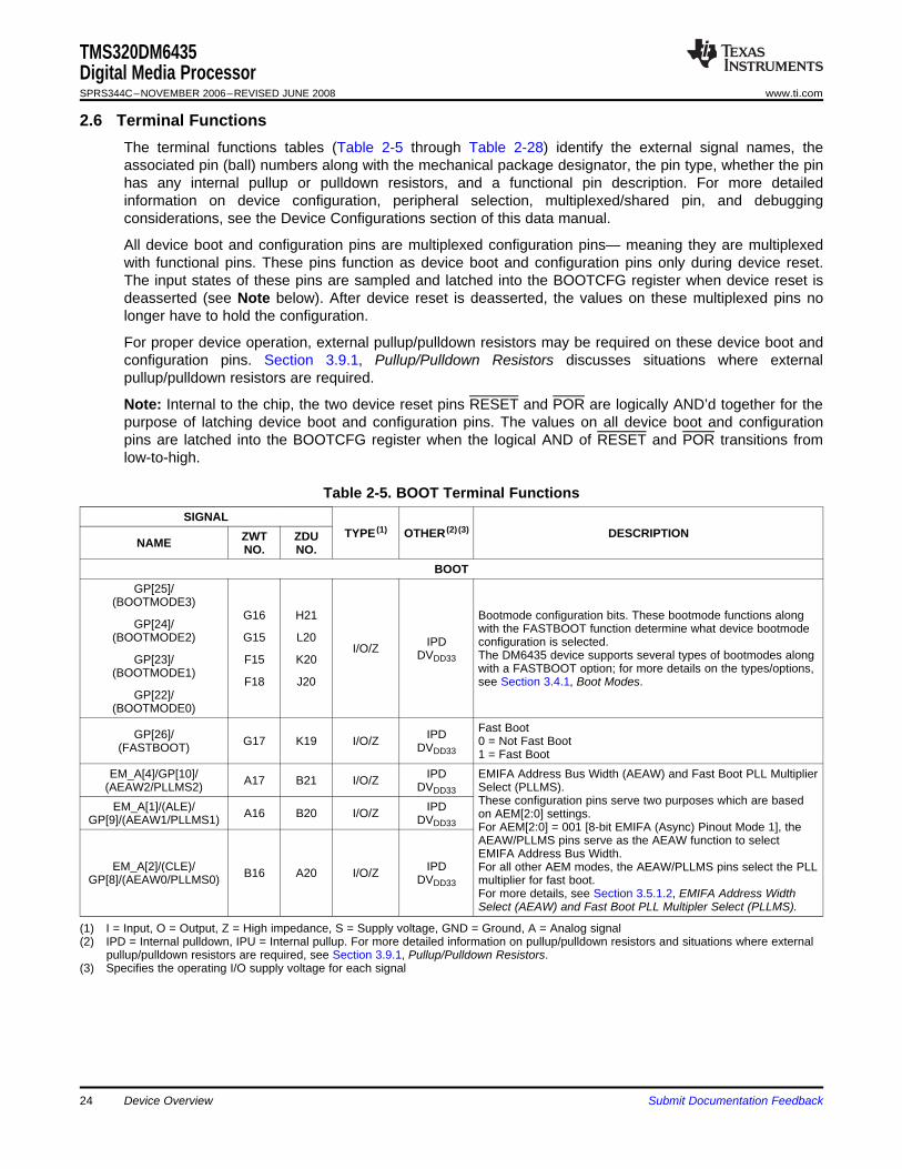
2.6 Terminal Functions
TMS320DM6435Digital Media ProcessorSPRS344C–NOVEMBER 2006–REVISED JUNE 2008 www.ti.com
The terminal functions tables (Table 2-5 through Table 2-28) identify the external signal names, theassociated pin (ball) numbers along with the mechanical package designator, the pin type, whether the pinhas any internal pullup or pulldown resistors, and a functional pin description. For more detailedinformation on device configuration, peripheral selection, multiplexed/shared pin, and debuggingconsiderations, see the Device Configurations section of this data manual.
All device boot and configuration pins are multiplexed configuration pins— meaning they are multiplexedwith functional pins. These pins function as device boot and configuration pins only during device reset.The input states of these pins are sampled and latched into the BOOTCFG register when device reset isdeasserted (see Note below). After device reset is deasserted, the values on these multiplexed pins nolonger have to hold the configuration.
For proper device operation, external pullup/pulldown resistors may be required on these device boot andconfiguration pins. Section 3.9.1, Pullup/Pulldown Resistors discusses situations where externalpullup/pulldown resistors are required.
Note: Internal to the chip, the two device reset pins RESET and POR are logically AND’d together for thepurpose of latching device boot and configuration pins. The values on all device boot and configurationpins are latched into the BOOTCFG register when the logical AND of RESET and POR transitions fromlow-to-high.
Table 2-5. BOOT Terminal FunctionsSIGNAL
TYPE (1) OTHER (2) (3) DESCRIPTIONZWT ZDUNAME NO. NO.BOOT
GP[25]/(BOOTMODE3)
G16 H21 Bootmode configuration bits. These bootmode functions alongGP[24]/ with the FASTBOOT function determine what device bootmode
(BOOTMODE2) G15 L20 IPD configuration is selected.I/O/Z DVDD33 The DM6435 device supports several types of bootmodes alongGP[23]/ F15 K20with a FASTBOOT option; for more details on the types/options,(BOOTMODE1)
F18 J20 see Section 3.4.1, Boot Modes.GP[22]/
(BOOTMODE0)Fast BootGP[26]/ IPDG17 K19 I/O/Z 0 = Not Fast Boot(FASTBOOT) DVDD33 1 = Fast Boot
EM_A[4]/GP[10]/ IPD EMIFA Address Bus Width (AEAW) and Fast Boot PLL MultiplierA17 B21 I/O/Z(AEAW2/PLLMS2) DVDD33 Select (PLLMS).These configuration pins serve two purposes which are basedEM_A[1]/(ALE)/ IPDA16 B20 I/O/Z on AEM[2:0] settings.GP[9]/(AEAW1/PLLMS1) DVDD33 For AEM[2:0] = 001 [8-bit EMIFA (Async) Pinout Mode 1], theAEAW/PLLMS pins serve as the AEAW function to selectEMIFA Address Bus Width.
EM_A[2]/(CLE)/ IPD For all other AEM modes, the AEAW/PLLMS pins select the PLLB16 A20 I/O/ZGP[8]/(AEAW0/PLLMS0) DVDD33 multiplier for fast boot.For more details, see Section 3.5.1.2, EMIFA Address WidthSelect (AEAW) and Fast Boot PLL Multipler Select (PLLMS).
(1) I = Input, O = Output, Z = High impedance, S = Supply voltage, GND = Ground, A = Analog signal(2) IPD = Internal pulldown, IPU = Internal pullup. For more detailed information on pullup/pulldown resistors and situations where external
pullup/pulldown resistors are required, see Section 3.9.1, Pullup/Pulldown Resistors.(3) Specifies the operating I/O supply voltage for each signal
24 Device Overview Submit Documentation Feedback
TMS320DM6435Digital Media Processor
www.ti.com SPRS344C–NOVEMBER 2006–REVISED JUNE 2008
Table 2-5. BOOT Terminal Functions (continued)SIGNAL
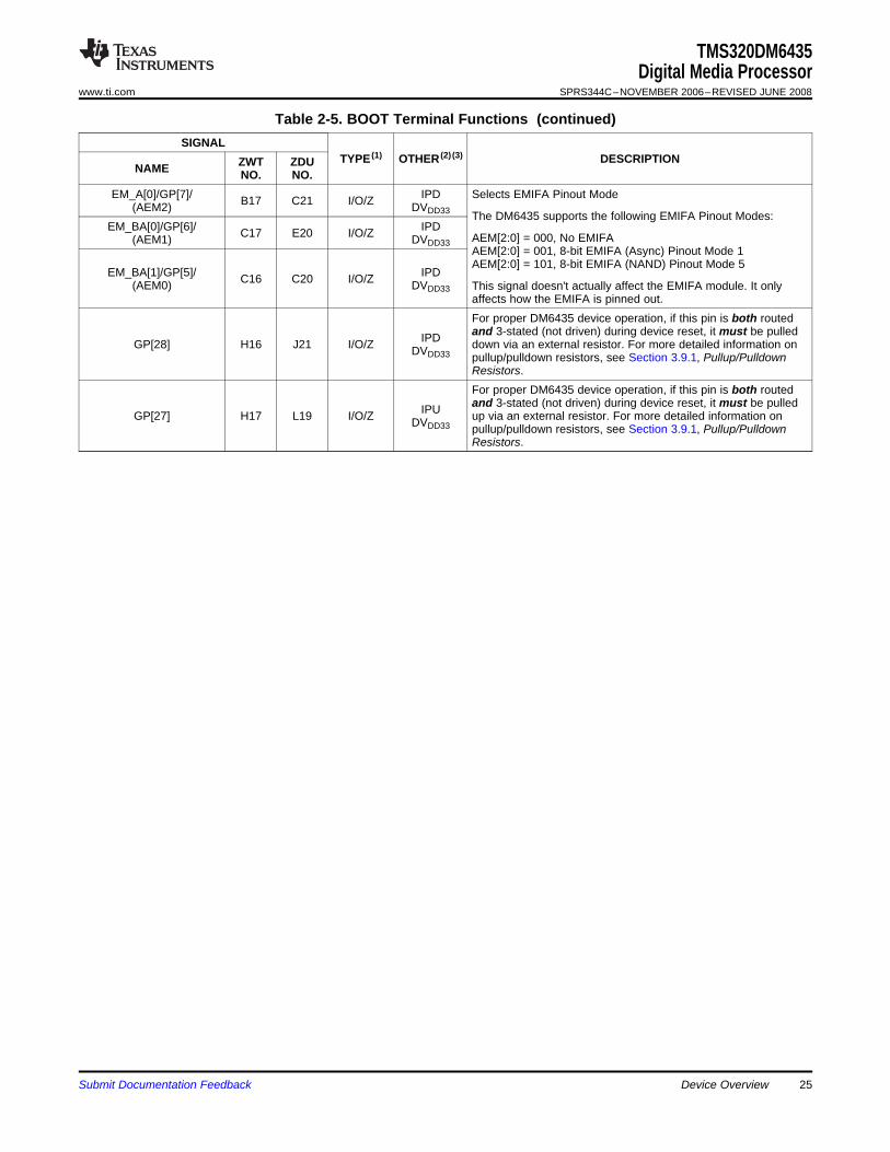
TYPE (1) OTHER (2) (3) DESCRIPTIONZWT ZDUNAME NO. NO.EM_A[0]/GP[7]/ IPD Selects EMIFA Pinout ModeB17 C21 I/O/Z(AEM2) DVDD33 The DM6435 supports the following EMIFA Pinout Modes:
EM_BA[0]/GP[6]/ IPDC17 E20 I/O/Z AEM[2:0] = 000, No EMIFA(AEM1) DVDD33AEM[2:0] = 001, 8-bit EMIFA (Async) Pinout Mode 1AEM[2:0] = 101, 8-bit EMIFA (NAND) Pinout Mode 5
EM_BA[1]/GP[5]/ IPDC16 C20 I/O/Z(AEM0) DVDD33 This signal doesn't actually affect the EMIFA module. It onlyaffects how the EMIFA is pinned out.For proper DM6435 device operation, if this pin is both routedand 3-stated (not driven) during device reset, it must be pulledIPDGP[28] H16 J21 I/O/Z down via an external resistor. For more detailed information onDVDD33 pullup/pulldown resistors, see Section 3.9.1, Pullup/PulldownResistors.For proper DM6435 device operation, if this pin is both routedand 3-stated (not driven) during device reset, it must be pulledIPUGP[27] H17 L19 I/O/Z up via an external resistor. For more detailed information onDVDD33 pullup/pulldown resistors, see Section 3.9.1, Pullup/PulldownResistors.
Submit Documentation Feedback Device Overview 25
TMS320DM6435Digital Media ProcessorSPRS344C–NOVEMBER 2006–REVISED JUNE 2008 www.ti.com
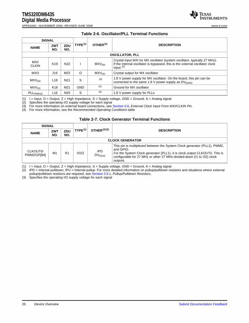
Table 2-6. Oscillator/PLL Terminal FunctionsSIGNAL
TYPE (1) OTHER (2) DESCRIPTIONZWT ZDUNAME NO. NO.OSCILLATOR, PLL
Crystal input MXI for MX oscillator (system oscillator, typically 27 MHz).MXI/ K19 N22 I MXVDD If the internal oscillator is bypassed, this is the external oscillator clockCLKIN input. (3)
MXO J19 M22 O MXVDD Crystal output for MX oscillator1.8 V power supply for MX oscillator. On the board, this pin can beMXVDD L18 N21 S (4)connected to the same 1.8 V power supply as DVDDR2.
MXVSS K18 M21 GND (4) Ground for MX oscillatorPLLPWR18 L16 N20 S (4) 1.8 V power supply for PLLs
(1) I = Input, O = Output, Z = High impedance, S = Supply voltage, GND = Ground, A = Analog signal(2) Specifies the operating I/O supply voltage for each signal(3) For more information on external board connections, see Section 6.6, External Clock Input From MXI/CLKIN Pin.(4) For more information, see the Recommended Operating Conditions table
Table 2-7. Clock Generator Terminal FunctionsSIGNAL
TYPE (1) OTHER (2) (3) DESCRIPTIONZWT ZDUNAME NO. NO.CLOCK GENERATOR
This pin is multiplexed between the System Clock generator (PLL1), PWM2,and GPIO.CLKOUT0/ IPDM1 R1 I/O/Z For the System Clock generator (PLL1), it is clock output CLKOUT0. This isPWM2/GP[84] DVDD33 configurable for 27 MHz or other 27 MHz-divided-down (/1 to /32) clockoutputs.
(1) I = Input, O = Output, Z = High impedance, S = Supply voltage, GND = Ground, A = Analog signal(2) IPD = Internal pulldown, IPU = Internal pullup. For more detailed information on pullup/pulldown resistors and situations where external
pullup/pulldown resistors are required, see Section 3.9.1, Pullup/Pulldown Resistors.(3) Specifies the operating I/O supply voltage for each signal
Device Overview26 Submit Documentation Feedback

TMS320DM6435Digital Media Processor
www.ti.com SPRS344C–NOVEMBER 2006–REVISED JUNE 2008
Table 2-8. RESET and JTAG Terminal FunctionsSIGNAL
TYPE (1) OTHER (2) (3) DESCRIPTIONZWT ZDUNAME NO. NO.RESET
IPURESET M4 R3 I Device resetDVDD33
– Reset output status pin. The RESETOUT pin indicates when theRESETOUT N3 T3 O/Z DVDD33 device is in reset.IPUPOR N4 R2 I Power-on reset.DVDD33
JTAGIPU JTAG test-port mode select input.TMS R3 V3 I DVDD33 For proper device operation, do not oppose the IPU on this pin.–TDO P3 U2 O/Z JTAG test-port data outputDVDD33
IPUTDI P4 U3 I JTAG test-port data inputDVDD33
IPUTCK N1 U1 I JTAG test-port clock inputDVDD33
JTAG test-port reset. For IEEE 1149.1 JTAG compatibility, seeIPDTRST R2 V2 I the IEEE 1149.1 JTAG compatibility statement portion of this dataDVDD33 sheetIPUEMU1 N2 T2 I/O/Z Emulation pin 1DVDD33
IPUEMU0 P2 T1 I/O/Z Emulation pin 0DVDD33
(1) I = Input, O = Output, Z = High impedance, S = Supply voltage, GND = Ground, A = Analog signal(2) IPD = Internal pulldown, IPU = Internal pullup. For more detailed information on pullup/pulldown resistors and situations where external
pullup/pulldown resistors are required, see Section 3.9.1, Pullup/Pulldown Resistors.(3) Specifies the operating I/O supply voltage for each signal
Submit Documentation Feedback Device Overview 27
TMS320DM6435Digital Media ProcessorSPRS344C–NOVEMBER 2006–REVISED JUNE 2008 www.ti.com
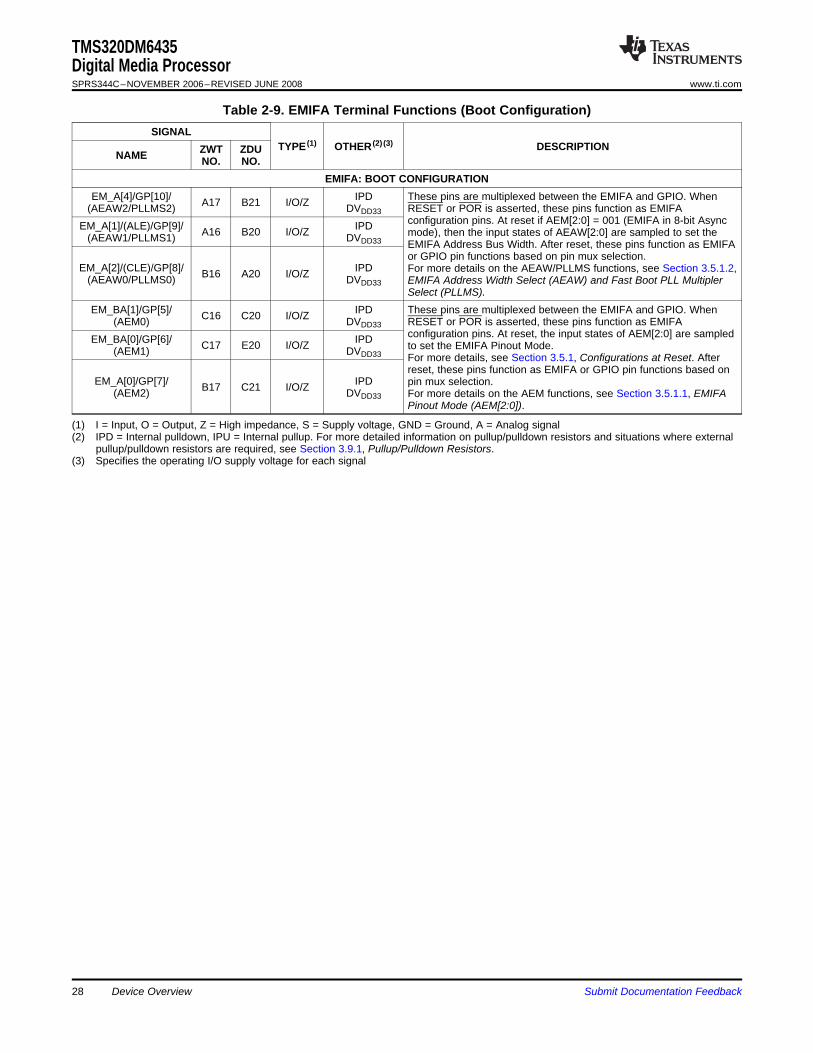
Table 2-9. EMIFA Terminal Functions (Boot Configuration)SIGNAL
TYPE (1) OTHER (2) (3) DESCRIPTIONZWT ZDUNAME NO. NO.EMIFA: BOOT CONFIGURATION
EM_A[4]/GP[10]/ IPD These pins are multiplexed between the EMIFA and GPIO. WhenA17 B21 I/O/Z(AEAW2/PLLMS2) DVDD33 RESET or POR is asserted, these pins function as EMIFAconfiguration pins. At reset if AEM[2:0] = 001 (EMIFA in 8-bit AsyncEM_A[1]/(ALE)/GP[9]/ IPDA16 B20 I/O/Z mode), then the input states of AEAW[2:0] are sampled to set the(AEAW1/PLLMS1) DVDD33 EMIFA Address Bus Width. After reset, these pins function as EMIFAor GPIO pin functions based on pin mux selection.
EM_A[2]/(CLE)/GP[8]/ IPD For more details on the AEAW/PLLMS functions, see Section 3.5.1.2,B16 A20 I/O/Z(AEAW0/PLLMS0) DVDD33 EMIFA Address Width Select (AEAW) and Fast Boot PLL MultiplerSelect (PLLMS).
EM_BA[1]/GP[5]/ IPD These pins are multiplexed between the EMIFA and GPIO. WhenC16 C20 I/O/Z(AEM0) DVDD33 RESET or POR is asserted, these pins function as EMIFAconfiguration pins. At reset, the input states of AEM[2:0] are sampledEM_BA[0]/GP[6]/ IPDC17 E20 I/O/Z to set the EMIFA Pinout Mode.(AEM1) DVDD33 For more details, see Section 3.5.1, Configurations at Reset. Afterreset, these pins function as EMIFA or GPIO pin functions based on
EM_A[0]/GP[7]/ IPD pin mux selection.B17 C21 I/O/Z(AEM2) DVDD33 For more details on the AEM functions, see Section 3.5.1.1, EMIFAPinout Mode (AEM[2:0]).
(1) I = Input, O = Output, Z = High impedance, S = Supply voltage, GND = Ground, A = Analog signal(2) IPD = Internal pulldown, IPU = Internal pullup. For more detailed information on pullup/pulldown resistors and situations where external
pullup/pulldown resistors are required, see Section 3.9.1, Pullup/Pulldown Resistors.(3) Specifies the operating I/O supply voltage for each signal
Device Overview28 Submit Documentation Feedback
TMS320DM6435Digital Media Processor
www.ti.com SPRS344C–NOVEMBER 2006–REVISED JUNE 2008
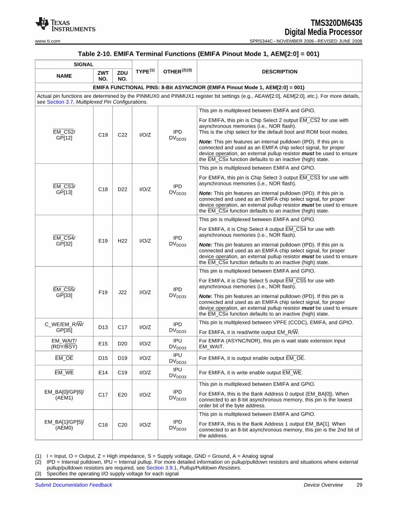
Table 2-10. EMIFA Terminal Functions (EMIFA Pinout Mode 1, AEM[2:0] = 001)SIGNAL
TYPE (1) OTHER (2) (3) DESCRIPTIONZWT ZDUNAME NO. NO.EMIFA FUNCTIONAL PINS: 8-Bit ASYNC/NOR (EMIFA Pinout Mode 1, AEM[2:0] = 001)
Actual pin functions are determined by the PINMUX0 and PINMUX1 register bit settings (e.g., AEAW[2:0], AEM[2:0], etc.). For more details,see Section 3.7, Multiplexed Pin Configurations.
This pin is multiplexed between EMIFA and GPIO.
For EMIFA, this pin is Chip Select 2 output EM_CS2 for use withasynchronous memories (i.e., NOR flash).
EM_CS2/ IPD This is the chip select for the default boot and ROM boot modes.C19 C22 I/O/ZGP[12] DVDD33 Note: This pin features an internal pulldown (IPD). If this pin isconnected and used as an EMIFA chip select signal, for properdevice operation, an external pullup resistor must be used to ensurethe EM_CSx function defaults to an inactive (high) state.This pin is multiplexed between EMIFA and GPIO.
For EMIFA, this pin is Chip Select 3 output EM_CS3 for use withasynchronous memories (i.e., NOR flash).EM_CS3/ IPDC18 D22 I/O/ZGP[13] DVDD33 Note: This pin features an internal pulldown (IPD). If this pin isconnected and used as an EMIFA chip select signal, for properdevice operation, an external pullup resistor must be used to ensurethe EM_CSx function defaults to an inactive (high) state.This pin is multiplexed between EMIFA and GPIO.
For EMIFA, it is Chip Select 4 output EM_CS4 for use withasynchronous memories (i.e., NOR flash).EM_CS4/ IPDE19 H22 I/O/ZGP[32] DVDD33 Note: This pin features an internal pulldown (IPD). If this pin isconnected and used as an EMIFA chip select signal, for properdevice operation, an external pullup resistor must be used to ensurethe EM_CSx function defaults to an inactive (high) state.This pin is multiplexed between EMIFA and GPIO.
For EMIFA, it is Chip Select 5 output EM_CS5 for use withasynchronous memories (i.e., NOR flash).EM_CS5/ IPDF19 J22 I/O/ZGP[33] DVDD33 Note: This pin features an internal pulldown (IPD). If this pin isconnected and used as an EMIFA chip select signal, for properdevice operation, an external pullup resistor must be used to ensurethe EM_CSx function defaults to an inactive (high) state.This pin is multiplexed between VPFE (CCDC), EMIFA, and GPIO.C_WE/EM_R/W/ IPDD13 C17 I/O/ZGP[35] DVDD33 For EMIFA, it is read/write output EM_R/W.
EM_WAIT/ IPU For EMIFA (ASYNC/NOR), this pin is wait state extension inputE15 D20 I/O/Z(RDY/BSY) DVDD33 EM_WAIT.IPUEM_OE D15 D19 I/O/Z For EMIFA, it is output enable output EM_OE.DVDD33
IPUEM_WE E14 C19 I/O/Z For EMIFA, it is write enable output EM_WE.DVDD33
This pin is multiplexed between EMIFA and GPIO.EM_BA[0]/GP[6]/ IPD For EMIFA, this is the Bank Address 0 output (EM_BA[0]). WhenC17 E20 I/O/Z(AEM1) DVDD33 connected to an 8-bit asynchronous memory, this pin is the lowest
order bit of the byte address.This pin is multiplexed between EMIFA and GPIO.
EM_BA[1]/GP[5]/ IPD For EMIFA, this is the Bank Address 1 output EM_BA[1]. WhenC16 C20 I/O/Z(AEM0) DVDD33 connected to an 8-bit asynchronous memory, this pin is the 2nd bit ofthe address.
(1) I = Input, O = Output, Z = High impedance, S = Supply voltage, GND = Ground, A = Analog signal(2) IPD = Internal pulldown, IPU = Internal pullup. For more detailed information on pullup/pulldown resistors and situations where external
pullup/pulldown resistors are required, see Section 3.9.1, Pullup/Pulldown Resistors.(3) Specifies the operating I/O supply voltage for each signal
Submit Documentation Feedback Device Overview 29
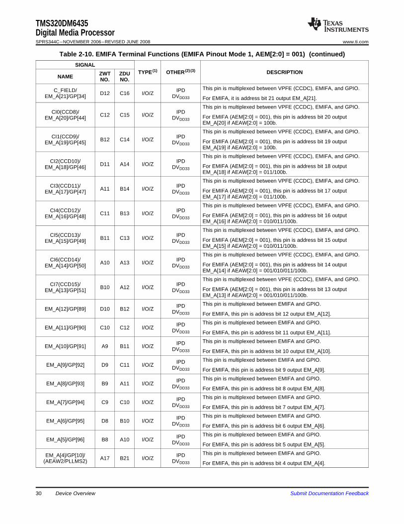
TMS320DM6435Digital Media ProcessorSPRS344C–NOVEMBER 2006–REVISED JUNE 2008 www.ti.com
Table 2-10. EMIFA Terminal Functions (EMIFA Pinout Mode 1, AEM[2:0] = 001) (continued)SIGNAL
TYPE (1) OTHER (2) (3) DESCRIPTIONZWT ZDUNAME NO. NO.This pin is multiplexed between VPFE (CCDC), EMIFA, and GPIO.C_FIELD/ IPDD12 C16 I/O/ZEM_A[21]/GP[34] DVDD33 For EMIFA, it is address bit 21 output EM_A[21].This pin is multiplexed between VPFE (CCDC), EMIFA, and GPIO.
CI0(CCD8)/ IPDC12 C15 I/O/Z For EMIFA (AEM[2:0] = 001), this pin is address bit 20 outputEM_A[20]/GP[44] DVDD33EM_A[20] if AEAW[2:0] = 100b.This pin is multiplexed between VPFE (CCDC), EMIFA, and GPIO.
CI1(CCD9)/ IPDB12 C14 I/O/Z For EMIFA (AEM[2:0] = 001), this pin is address bit 19 outputEM_A[19]/GP[45] DVDD33EM_A[19] if AEAW[2:0] = 100b.This pin is multiplexed between VPFE (CCDC), EMIFA, and GPIO.
CI2(CCD10)/ IPDD11 A14 I/O/Z For EMIFA (AEM[2:0] = 001), this pin is address bit 18 outputEM_A[18]/GP[46] DVDD33EM_A[18] if AEAW[2:0] = 011/100b.This pin is multiplexed between VPFE (CCDC), EMIFA, and GPIO.
CI3(CCD11)/ IPDA11 B14 I/O/Z For EMIFA (AEM[2:0] = 001), this pin is address bit 17 outputEM_A[17]/GP[47] DVDD33EM_A[17] if AEAW[2:0] = 011/100b.This pin is multiplexed between VPFE (CCDC), EMIFA, and GPIO.
CI4(CCD12)/ IPDC11 B13 I/O/Z For EMIFA (AEM[2:0] = 001), this pin is address bit 16 outputEM_A[16]/GP[48] DVDD33EM_A[16] if AEAW[2:0] = 010/011/100b.This pin is multiplexed between VPFE (CCDC), EMIFA, and GPIO.
CI5(CCD13)/ IPDB11 C13 I/O/Z For EMIFA (AEM[2:0] = 001), this pin is address bit 15 outputEM_A[15]/GP[49] DVDD33EM_A[15] if AEAW[2:0] = 010/011/100b.This pin is multiplexed between VPFE (CCDC), EMIFA, and GPIO.
CI6(CCD14)/ IPDA10 A13 I/O/Z For EMIFA (AEM[2:0] = 001), this pin is address bit 14 outputEM_A[14]/GP[50] DVDD33EM_A[14] if AEAW[2:0] = 001/010/011/100b.This pin is multiplexed between VPFE (CCDC), EMIFA, and GPIO.
CI7(CCD15)/ IPDB10 A12 I/O/Z For EMIFA (AEM[2:0] = 001), this pin is address bit 13 outputEM_A[13]/GP[51] DVDD33EM_A[13] if AEAW[2:0] = 001/010/011/100b.This pin is multiplexed between EMIFA and GPIO.IPDEM_A[12]/GP[89] D10 B12 I/O/Z DVDD33 For EMIFA, this pin is address bit 12 output EM_A[12].This pin is multiplexed between EMIFA and GPIO.IPDEM_A[11]/GP[90] C10 C12 I/O/Z DVDD33 For EMIFA, this pin is address bit 11 output EM_A[11].This pin is multiplexed between EMIFA and GPIO.IPDEM_A[10]/GP[91] A9 B11 I/O/Z DVDD33 For EMIFA, this pin is address bit 10 output EM_A[10].This pin is multiplexed between EMIFA and GPIO.IPDEM_A[9]/GP[92] D9 C11 I/O/Z DVDD33 For EMIFA, this pin is address bit 9 output EM_A[9].This pin is multiplexed between EMIFA and GPIO.IPDEM_A[8]/GP[93] B9 A11 I/O/Z DVDD33 For EMIFA, this pin is address bit 8 output EM_A[8].This pin is multiplexed between EMIFA and GPIO.IPDEM_A[7]/GP[94] C9 C10 I/O/Z DVDD33 For EMIFA, this pin is address bit 7 output EM_A[7].This pin is multiplexed between EMIFA and GPIO.IPDEM_A[6]/GP[95] D8 B10 I/O/Z DVDD33 For EMIFA, this pin is address bit 6 output EM_A[6].This pin is multiplexed between EMIFA and GPIO.IPDEM_A[5]/GP[96] B8 A10 I/O/Z DVDD33 For EMIFA, this pin is address bit 5 output EM_A[5].This pin is multiplexed between EMIFA and GPIO.EM_A[4]/GP[10]/ IPDA17 B21 I/O/Z(AEAW2/PLLMS2) DVDD33 For EMIFA, this pin is address bit 4 output EM_A[4].
Device Overview30 Submit Documentation Feedback
TMS320DM6435Digital Media Processor
www.ti.com SPRS344C–NOVEMBER 2006–REVISED JUNE 2008
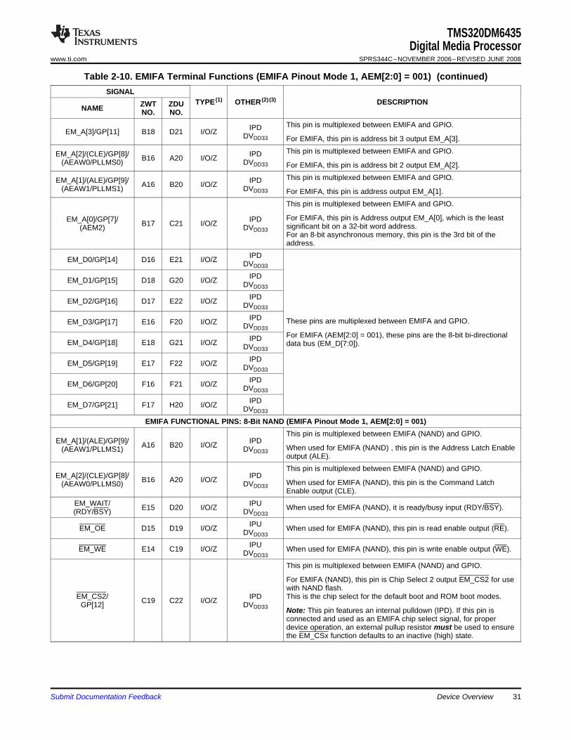
Table 2-10. EMIFA Terminal Functions (EMIFA Pinout Mode 1, AEM[2:0] = 001) (continued)SIGNAL
TYPE (1) OTHER (2) (3) DESCRIPTIONZWT ZDUNAME NO. NO.This pin is multiplexed between EMIFA and GPIO.IPDEM_A[3]/GP[11] B18 D21 I/O/Z DVDD33 For EMIFA, this pin is address bit 3 output EM_A[3].This pin is multiplexed between EMIFA and GPIO.EM_A[2]/(CLE)/GP[8]/ IPDB16 A20 I/O/Z(AEAW0/PLLMS0) DVDD33 For EMIFA, this pin is address bit 2 output EM_A[2].This pin is multiplexed between EMIFA and GPIO.EM_A[1]/(ALE)/GP[9]/ IPDA16 B20 I/O/Z(AEAW1/PLLMS1) DVDD33 For EMIFA, this pin is address output EM_A[1].This pin is multiplexed between EMIFA and GPIO.
For EMIFA, this pin is Address output EM_A[0], which is the leastEM_A[0]/GP[7]/ IPDB17 C21 I/O/Z significant bit on a 32-bit word address.(AEM2) DVDD33For an 8-bit asynchronous memory, this pin is the 3rd bit of theaddress.
IPDEM_D0/GP[14] D16 E21 I/O/Z DVDD33
IPDEM_D1/GP[15] D18 G20 I/O/Z DVDD33
IPDEM_D2/GP[16] D17 E22 I/O/Z DVDD33
IPD These pins are multiplexed between EMIFA and GPIO.EM_D3/GP[17] E16 F20 I/O/Z DVDD33For EMIFA (AEM[2:0] = 001), these pins are the 8-bit bi-directionalIPDEM_D4/GP[18] E18 G21 I/O/Z data bus (EM_D[7:0]).DVDD33
IPDEM_D5/GP[19] E17 F22 I/O/Z DVDD33
IPDEM_D6/GP[20] F16 F21 I/O/Z DVDD33
IPDEM_D7/GP[21] F17 H20 I/O/Z DVDD33
EMIFA FUNCTIONAL PINS: 8-Bit NAND (EMIFA Pinout Mode 1, AEM[2:0] = 001)This pin is multiplexed between EMIFA (NAND) and GPIO.
EM_A[1]/(ALE)/GP[9]/ IPDA16 B20 I/O/Z When used for EMIFA (NAND) , this pin is the Address Latch Enable(AEAW1/PLLMS1) DVDD33output (ALE).This pin is multiplexed between EMIFA (NAND) and GPIO.
EM_A[2]/(CLE)/GP[8]/ IPDB16 A20 I/O/Z When used for EMIFA (NAND), this pin is the Command Latch(AEAW0/PLLMS0) DVDD33Enable output (CLE).
EM_WAIT/ IPUE15 D20 I/O/Z When used for EMIFA (NAND), it is ready/busy input (RDY/BSY).(RDY/BSY) DVDD33
IPUEM_OE D15 D19 I/O/Z When used for EMIFA (NAND), this pin is read enable output (RE).DVDD33
IPUEM_WE E14 C19 I/O/Z When used for EMIFA (NAND), this pin is write enable output (WE).DVDD33
This pin is multiplexed between EMIFA (NAND) and GPIO.
For EMIFA (NAND), this pin is Chip Select 2 output EM_CS2 for usewith NAND flash.
EM_CS2/ IPD This is the chip select for the default boot and ROM boot modes.C19 C22 I/O/ZGP[12] DVDD33 Note: This pin features an internal pulldown (IPD). If this pin isconnected and used as an EMIFA chip select signal, for properdevice operation, an external pullup resistor must be used to ensurethe EM_CSx function defaults to an inactive (high) state.
Submit Documentation Feedback Device Overview 31
TMS320DM6435Digital Media ProcessorSPRS344C–NOVEMBER 2006–REVISED JUNE 2008 www.ti.com
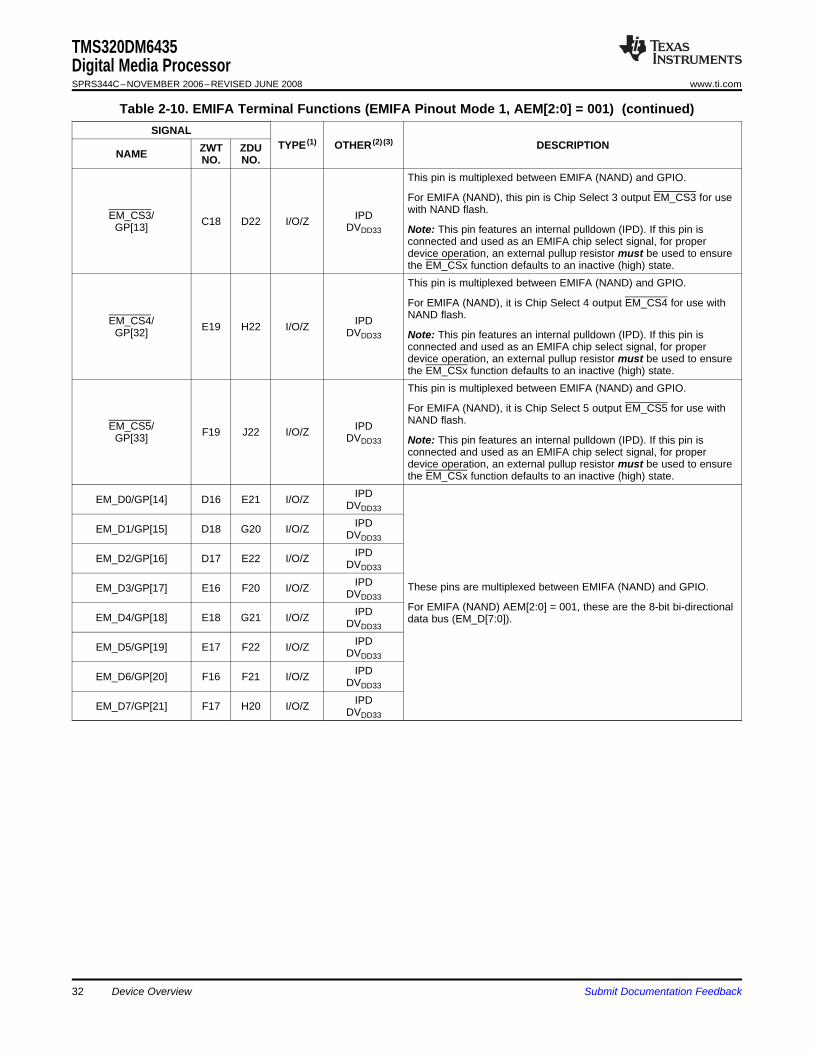
Table 2-10. EMIFA Terminal Functions (EMIFA Pinout Mode 1, AEM[2:0] = 001) (continued)SIGNAL
TYPE (1) OTHER (2) (3) DESCRIPTIONZWT ZDUNAME NO. NO.This pin is multiplexed between EMIFA (NAND) and GPIO.
For EMIFA (NAND), this pin is Chip Select 3 output EM_CS3 for usewith NAND flash.EM_CS3/ IPDC18 D22 I/O/ZGP[13] DVDD33 Note: This pin features an internal pulldown (IPD). If this pin isconnected and used as an EMIFA chip select signal, for properdevice operation, an external pullup resistor must be used to ensurethe EM_CSx function defaults to an inactive (high) state.This pin is multiplexed between EMIFA (NAND) and GPIO.
For EMIFA (NAND), it is Chip Select 4 output EM_CS4 for use withNAND flash.EM_CS4/ IPDE19 H22 I/O/ZGP[32] DVDD33 Note: This pin features an internal pulldown (IPD). If this pin isconnected and used as an EMIFA chip select signal, for properdevice operation, an external pullup resistor must be used to ensurethe EM_CSx function defaults to an inactive (high) state.This pin is multiplexed between EMIFA (NAND) and GPIO.
For EMIFA (NAND), it is Chip Select 5 output EM_CS5 for use withNAND flash.EM_CS5/ IPDF19 J22 I/O/ZGP[33] DVDD33 Note: This pin features an internal pulldown (IPD). If this pin isconnected and used as an EMIFA chip select signal, for properdevice operation, an external pullup resistor must be used to ensurethe EM_CSx function defaults to an inactive (high) state.
IPDEM_D0/GP[14] D16 E21 I/O/Z DVDD33
IPDEM_D1/GP[15] D18 G20 I/O/Z DVDD33
IPDEM_D2/GP[16] D17 E22 I/O/Z DVDD33
IPD These pins are multiplexed between EMIFA (NAND) and GPIO.EM_D3/GP[17] E16 F20 I/O/Z DVDD33For EMIFA (NAND) AEM[2:0] = 001, these are the 8-bit bi-directionalIPDEM_D4/GP[18] E18 G21 I/O/Z data bus (EM_D[7:0]).DVDD33
IPDEM_D5/GP[19] E17 F22 I/O/Z DVDD33
IPDEM_D6/GP[20] F16 F21 I/O/Z DVDD33
IPDEM_D7/GP[21] F17 H20 I/O/Z DVDD33
32 Device Overview Submit Documentation Feedback
TMS320DM6435Digital Media Processor
www.ti.com SPRS344C–NOVEMBER 2006–REVISED JUNE 2008
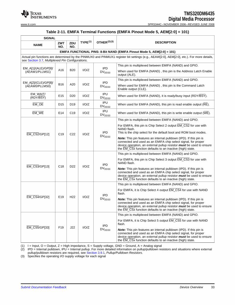
Table 2-11. EMIFA Terminal Functions (EMIFA Pinout Mode 5, AEM[2:0] = 101)SIGNAL
TYPE (1) OTHER (2) (3) DESCRIPTIONZWT ZDUNAME NO. NO.EMIFA FUNCTIONAL PINS: 8-Bit NAND (EMIFA Pinout Mode 5, AEM[2:0] = 101)
Actual pin functions are determined by the PINMUX0 and PINMUX1 register bit settings (e.g., AEAW[2:0], AEM[2:0], etc.). For more details,see Section 3.7, Multiplexed Pin Configurations.
This pin is multiplexed between EMIFA (NAND) and GPIO.EM_A[1]/(ALE)/GP[9]/ IPDA16 B20 I/O/Z When used for EMIFA (NAND) , this pin is the Address Latch Enable(AEAW1/PLLMS1) DVDD33
output (ALE).This pin is multiplexed between EMIFA (NAND) and GPIO.
EM_A[2]/(CLE)/GP[8]/ IPDB16 A20 I/O/Z When used for EMIFA (NAND) , this pin is the Command Latch(AEAW0/PLLMS0) DVDD33Enable output (CLE).
EM_WAIT/ IPUE15 D20 I/O/Z When used for EMIFA (NAND), it is ready/busy input (RDY/BSY).(RDY/BSY) DVDD33
IPUEM_OE D15 D19 I/O/Z When used for EMIFA (NAND), this pin is read enable output (RE).DVDD33
IPUEM_WE E14 C19 I/O/Z When used for EMIFA (NAND), this pin is write enable output (WE).DVDD33
This pin is multiplexed between EMIFA (NAND) and GPIO.
For EMIFA, this pin is Chip Select 2 output EM_CS2 for use withNAND flash.
IPD This is the chip select for the default boot and ROM boot modes.EM_CS2/GP[12] C19 C22 I/O/Z DVDD33 Note: This pin features an internal pulldown (IPD). If this pin isconnected and used as an EMIFA chip select signal, for properdevice operation, an external pullup resistor must be used to ensurethe EM_CSx function defaults to an inactive (high) state.This pin is multiplexed between EMIFA (NAND) and GPIO.
For EMIFA, this pin is Chip Select 3 output EM_CS3 for use withNAND flash.IPDEM_CS3/GP[13] C18 D22 I/O/Z DVDD33 Note: This pin features an internal pulldown (IPD). If this pin isconnected and used as an EMIFA chip select signal, for properdevice operation, an external pullup resistor must be used to ensurethe EM_CSx function defaults to an inactive (high) state.This pin is multiplexed between EMIFA (NAND) and GPIO.
For EMIFA, it is Chip Select 4 output EM_CS4 for use with NANDflash.IPDEM_CS4/GP[32] E19 H22 I/O/Z DVDD33 Note: This pin features an internal pulldown (IPD). If this pin isconnected and used as an EMIFA chip select signal, for properdevice operation, an external pullup resistor must be used to ensurethe EM_CSx function defaults to an inactive (high) state.This pin is multiplexed between EMIFA (NAND) and GPIO.
For EMIFA, it is Chip Select 5 output EM_CS5 for use with NANDflash.IPDEM_CS5/GP[33] F19 J22 I/O/Z DVDD33 Note: This pin features an internal pulldown (IPD). If this pin isconnected and used as an EMIFA chip select signal, for properdevice operation, an external pullup resistor must be used to ensurethe EM_CSx function defaults to an inactive (high) state.
(1) I = Input, O = Output, Z = High impedance, S = Supply voltage, GND = Ground, A = Analog signal(2) IPD = Internal pulldown, IPU = Internal pullup. For more detailed information on pullup/pulldown resistors and situations where external
pullup/pulldown resistors are required, see Section 3.9.1, Pullup/Pulldown Resistors.(3) Specifies the operating I/O supply voltage for each signal
Submit Documentation Feedback Device Overview 33
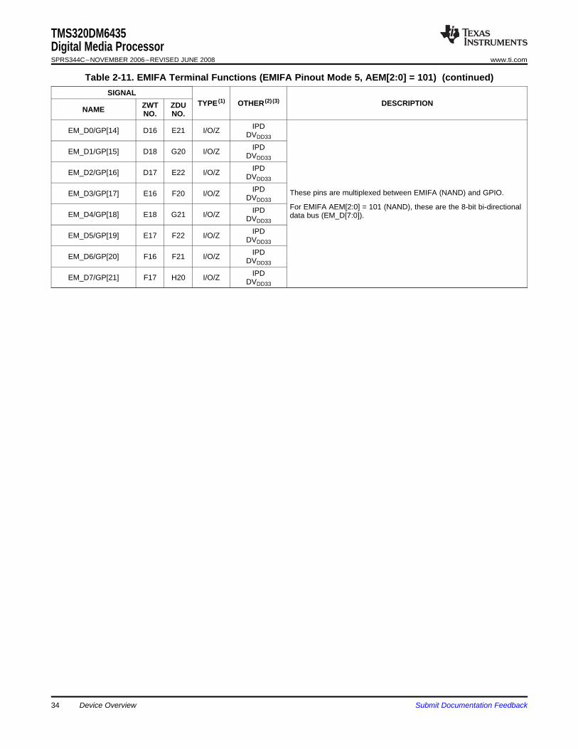
TMS320DM6435Digital Media ProcessorSPRS344C–NOVEMBER 2006–REVISED JUNE 2008 www.ti.com
Table 2-11. EMIFA Terminal Functions (EMIFA Pinout Mode 5, AEM[2:0] = 101) (continued)SIGNAL
TYPE (1) OTHER (2) (3) DESCRIPTIONZWT ZDUNAME NO. NO.IPDEM_D0/GP[14] D16 E21 I/O/Z DVDD33
IPDEM_D1/GP[15] D18 G20 I/O/Z DVDD33
IPDEM_D2/GP[16] D17 E22 I/O/Z DVDD33
IPD These pins are multiplexed between EMIFA (NAND) and GPIO.EM_D3/GP[17] E16 F20 I/O/Z DVDD33For EMIFA AEM[2:0] = 101 (NAND), these are the 8-bit bi-directionalIPDEM_D4/GP[18] E18 G21 I/O/Z data bus (EM_D[7:0]).DVDD33
IPDEM_D5/GP[19] E17 F22 I/O/Z DVDD33
IPDEM_D6/GP[20] F16 F21 I/O/Z DVDD33
IPDEM_D7/GP[21] F17 H20 I/O/Z DVDD33
Device Overview34 Submit Documentation Feedback
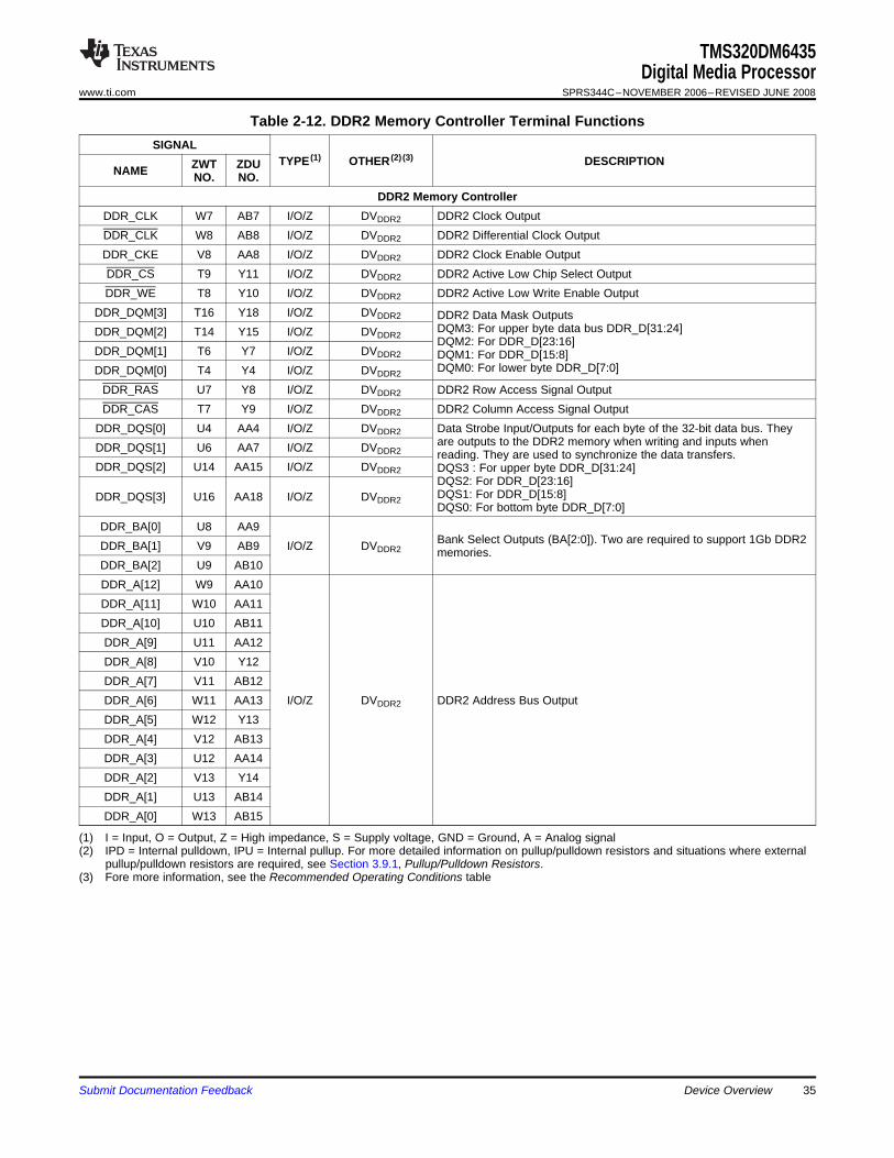
TMS320DM6435Digital Media Processor
www.ti.com SPRS344C–NOVEMBER 2006–REVISED JUNE 2008
Table 2-12. DDR2 Memory Controller Terminal FunctionsSIGNAL
TYPE (1) OTHER (2) (3) DESCRIPTIONZWT ZDUNAME NO. NO.DDR2 Memory Controller
DDR_CLK W7 AB7 I/O/Z DVDDR2 DDR2 Clock OutputDDR_CLK W8 AB8 I/O/Z DVDDR2 DDR2 Differential Clock OutputDDR_CKE V8 AA8 I/O/Z DVDDR2 DDR2 Clock Enable OutputDDR_CS T9 Y11 I/O/Z DVDDR2 DDR2 Active Low Chip Select OutputDDR_WE T8 Y10 I/O/Z DVDDR2 DDR2 Active Low Write Enable Output
DDR_DQM[3] T16 Y18 I/O/Z DVDDR2 DDR2 Data Mask OutputsDQM3: For upper byte data bus DDR_D[31:24]DDR_DQM[2] T14 Y15 I/O/Z DVDDR2 DQM2: For DDR_D[23:16]
DDR_DQM[1] T6 Y7 I/O/Z DVDDR2 DQM1: For DDR_D[15:8]DQM0: For lower byte DDR_D[7:0]DDR_DQM[0] T4 Y4 I/O/Z DVDDR2
DDR_RAS U7 Y8 I/O/Z DVDDR2 DDR2 Row Access Signal OutputDDR_CAS T7 Y9 I/O/Z DVDDR2 DDR2 Column Access Signal Output
DDR_DQS[0] U4 AA4 I/O/Z DVDDR2 Data Strobe Input/Outputs for each byte of the 32-bit data bus. Theyare outputs to the DDR2 memory when writing and inputs whenDDR_DQS[1] U6 AA7 I/O/Z DVDDR2 reading. They are used to synchronize the data transfers.
DDR_DQS[2] U14 AA15 I/O/Z DVDDR2 DQS3 : For upper byte DDR_D[31:24]DQS2: For DDR_D[23:16]DQS1: For DDR_D[15:8]DDR_DQS[3] U16 AA18 I/O/Z DVDDR2DQS0: For bottom byte DDR_D[7:0]
DDR_BA[0] U8 AA9Bank Select Outputs (BA[2:0]). Two are required to support 1Gb DDR2DDR_BA[1] V9 AB9 I/O/Z DVDDR2 memories.
DDR_BA[2] U9 AB10DDR_A[12] W9 AA10DDR_A[11] W10 AA11DDR_A[10] U10 AB11DDR_A[9] U11 AA12DDR_A[8] V10 Y12DDR_A[7] V11 AB12DDR_A[6] W11 AA13 I/O/Z DVDDR2 DDR2 Address Bus OutputDDR_A[5] W12 Y13DDR_A[4] V12 AB13DDR_A[3] U12 AA14DDR_A[2] V13 Y14DDR_A[1] U13 AB14DDR_A[0] W13 AB15
(1) I = Input, O = Output, Z = High impedance, S = Supply voltage, GND = Ground, A = Analog signal(2) IPD = Internal pulldown, IPU = Internal pullup. For more detailed information on pullup/pulldown resistors and situations where external
pullup/pulldown resistors are required, see Section 3.9.1, Pullup/Pulldown Resistors.(3) Fore more information, see the Recommended Operating Conditions table
Submit Documentation Feedback Device Overview 35

TMS320DM6435Digital Media ProcessorSPRS344C–NOVEMBER 2006–REVISED JUNE 2008 www.ti.com
Table 2-12. DDR2 Memory Controller Terminal Functions (continued)SIGNAL
TYPE (1) OTHER (2) (3) DESCRIPTIONZWT ZDUNAME NO. NO.DDR_D[31] T19 Y22DDR_D[30] U19 AA21DDR_D[29] V18 Y21DDR_D[28] U18 AB20DDR_D[27] W17 Y20DDR_D[26] T18 AA20DDR_D[25] U17 AB19DDR_D[24] V17 Y19DDR_D[23] T17 AA19DDR_D[22] V16 AB18DDR_D[21] W16 AB17DDR_D[20] U15 Y17DDR_D[19] V15 AA17DDR_D[18] W15 AB16DDR_D[17] V14 Y16DDR_D[16] W14 AA16 DDR2 bi-directional data bus can be configured as 32-bits wide orI/O/Z DVDDR2 16-bits wide.DDR_D[15] V7 AB6DDR_D[14] W6 Y6DDR_D[13] V6 AA6DDR_D[12] W5 AB5DDR_D[11] V5 Y5DDR_D[10] U5 AA5DDR_D[9] W4 W5DDR_D[8] V4 AB4DDR_D[7] W3 W4DDR_D[6] V3 AB3DDR_D[5] U3 Y3DDR_D[4] V2 AA3DDR_D[3] U2 AA2DDR_D[2] U1 W2DDR_D[1] T2 Y2DDR_D[0] T1 Y1
DDR_VREF T15 W18 I (3) Reference voltage input for the SSTL_18 I/O buffersDDR_VSSDLL T13 W15 GND (3) Ground for the DDR2 DLLDDR_VDDDLL T12 W14 S (3) Power (1.8 Volts) for the DDR2 Digital Locked Loop
Impedance control for DDR2 outputs. This must be connected via aDDR_ZN T10 W12 (3)200-Ω resistor to DVDDR2.Impedance control for DDR2 outputs. This must be connected via aDDR_ZP T11 W13 (3)200-Ω resistor to VSS.
Device Overview36 Submit Documentation Feedback
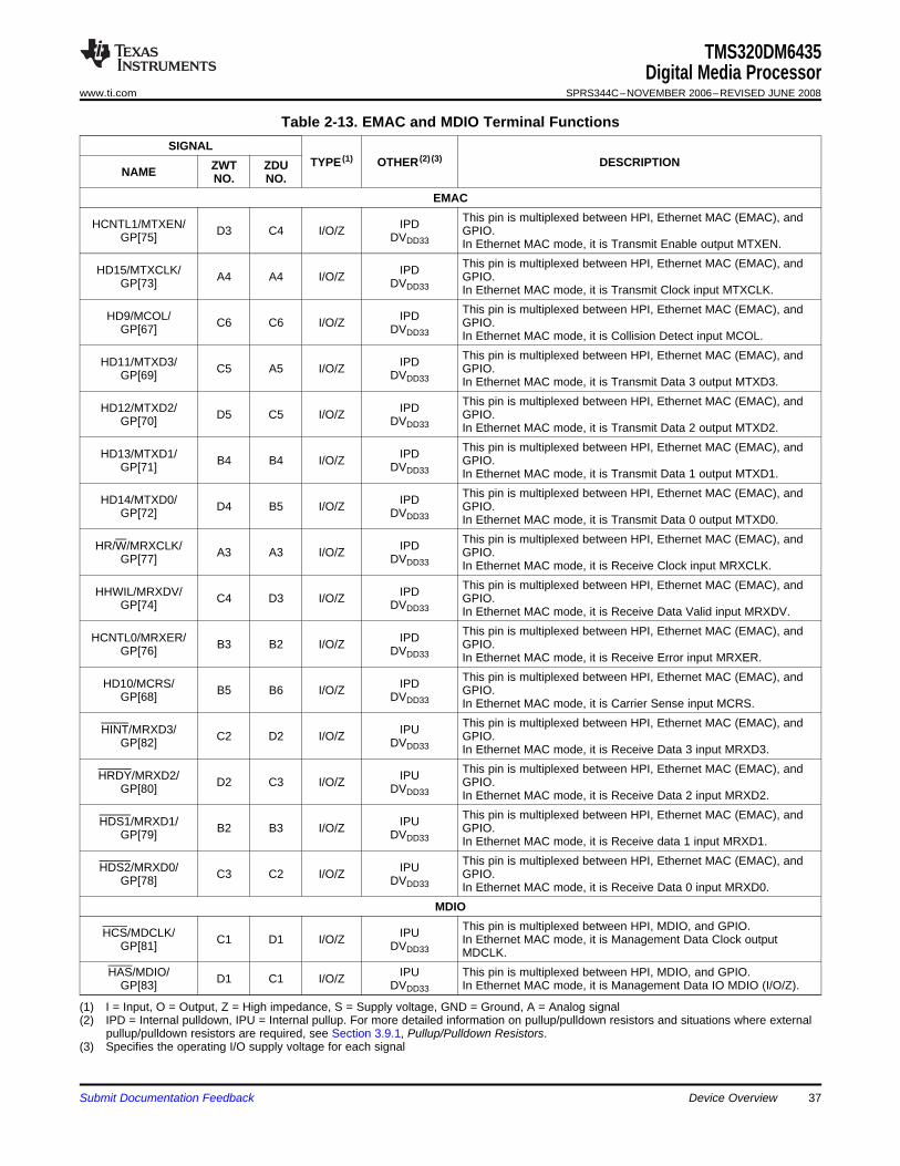
TMS320DM6435Digital Media Processor
www.ti.com SPRS344C–NOVEMBER 2006–REVISED JUNE 2008
Table 2-13. EMAC and MDIO Terminal FunctionsSIGNAL
TYPE (1) OTHER (2) (3) DESCRIPTIONZWT ZDUNAME NO. NO.EMAC
This pin is multiplexed between HPI, Ethernet MAC (EMAC), andHCNTL1/MTXEN/ IPDD3 C4 I/O/Z GPIO.GP[75] DVDD33 In Ethernet MAC mode, it is Transmit Enable output MTXEN.This pin is multiplexed between HPI, Ethernet MAC (EMAC), andHD15/MTXCLK/ IPDA4 A4 I/O/Z GPIO.GP[73] DVDD33 In Ethernet MAC mode, it is Transmit Clock input MTXCLK.This pin is multiplexed between HPI, Ethernet MAC (EMAC), andHD9/MCOL/ IPDC6 C6 I/O/Z GPIO.GP[67] DVDD33 In Ethernet MAC mode, it is Collision Detect input MCOL.This pin is multiplexed between HPI, Ethernet MAC (EMAC), andHD11/MTXD3/ IPDC5 A5 I/O/Z GPIO.GP[69] DVDD33 In Ethernet MAC mode, it is Transmit Data 3 output MTXD3.This pin is multiplexed between HPI, Ethernet MAC (EMAC), andHD12/MTXD2/ IPDD5 C5 I/O/Z GPIO.GP[70] DVDD33 In Ethernet MAC mode, it is Transmit Data 2 output MTXD2.This pin is multiplexed between HPI, Ethernet MAC (EMAC), andHD13/MTXD1/ IPDB4 B4 I/O/Z GPIO.GP[71] DVDD33 In Ethernet MAC mode, it is Transmit Data 1 output MTXD1.This pin is multiplexed between HPI, Ethernet MAC (EMAC), andHD14/MTXD0/ IPDD4 B5 I/O/Z GPIO.GP[72] DVDD33 In Ethernet MAC mode, it is Transmit Data 0 output MTXD0.This pin is multiplexed between HPI, Ethernet MAC (EMAC), andHR/W/MRXCLK/ IPDA3 A3 I/O/Z GPIO.GP[77] DVDD33 In Ethernet MAC mode, it is Receive Clock input MRXCLK.This pin is multiplexed between HPI, Ethernet MAC (EMAC), andHHWIL/MRXDV/ IPDC4 D3 I/O/Z GPIO.GP[74] DVDD33 In Ethernet MAC mode, it is Receive Data Valid input MRXDV.This pin is multiplexed between HPI, Ethernet MAC (EMAC), andHCNTL0/MRXER/ IPDB3 B2 I/O/Z GPIO.GP[76] DVDD33 In Ethernet MAC mode, it is Receive Error input MRXER.This pin is multiplexed between HPI, Ethernet MAC (EMAC), andHD10/MCRS/ IPDB5 B6 I/O/Z GPIO.GP[68] DVDD33 In Ethernet MAC mode, it is Carrier Sense input MCRS.This pin is multiplexed between HPI, Ethernet MAC (EMAC), andHINT/MRXD3/ IPUC2 D2 I/O/Z GPIO.GP[82] DVDD33 In Ethernet MAC mode, it is Receive Data 3 input MRXD3.This pin is multiplexed between HPI, Ethernet MAC (EMAC), andHRDY/MRXD2/ IPUD2 C3 I/O/Z GPIO.GP[80] DVDD33 In Ethernet MAC mode, it is Receive Data 2 input MRXD2.This pin is multiplexed between HPI, Ethernet MAC (EMAC), andHDS1/MRXD1/ IPUB2 B3 I/O/Z GPIO.GP[79] DVDD33 In Ethernet MAC mode, it is Receive data 1 input MRXD1.This pin is multiplexed between HPI, Ethernet MAC (EMAC), andHDS2/MRXD0/ IPUC3 C2 I/O/Z GPIO.GP[78] DVDD33 In Ethernet MAC mode, it is Receive Data 0 input MRXD0.
MDIOThis pin is multiplexed between HPI, MDIO, and GPIO.HCS/MDCLK/ IPUC1 D1 I/O/Z In Ethernet MAC mode, it is Management Data Clock outputGP[81] DVDD33 MDCLK.
HAS/MDIO/ IPU This pin is multiplexed between HPI, MDIO, and GPIO.D1 C1 I/O/ZGP[83] DVDD33 In Ethernet MAC mode, it is Management Data IO MDIO (I/O/Z).
(1) I = Input, O = Output, Z = High impedance, S = Supply voltage, GND = Ground, A = Analog signal(2) IPD = Internal pulldown, IPU = Internal pullup. For more detailed information on pullup/pulldown resistors and situations where external
pullup/pulldown resistors are required, see Section 3.9.1, Pullup/Pulldown Resistors.(3) Specifies the operating I/O supply voltage for each signal
Submit Documentation Feedback Device Overview 37
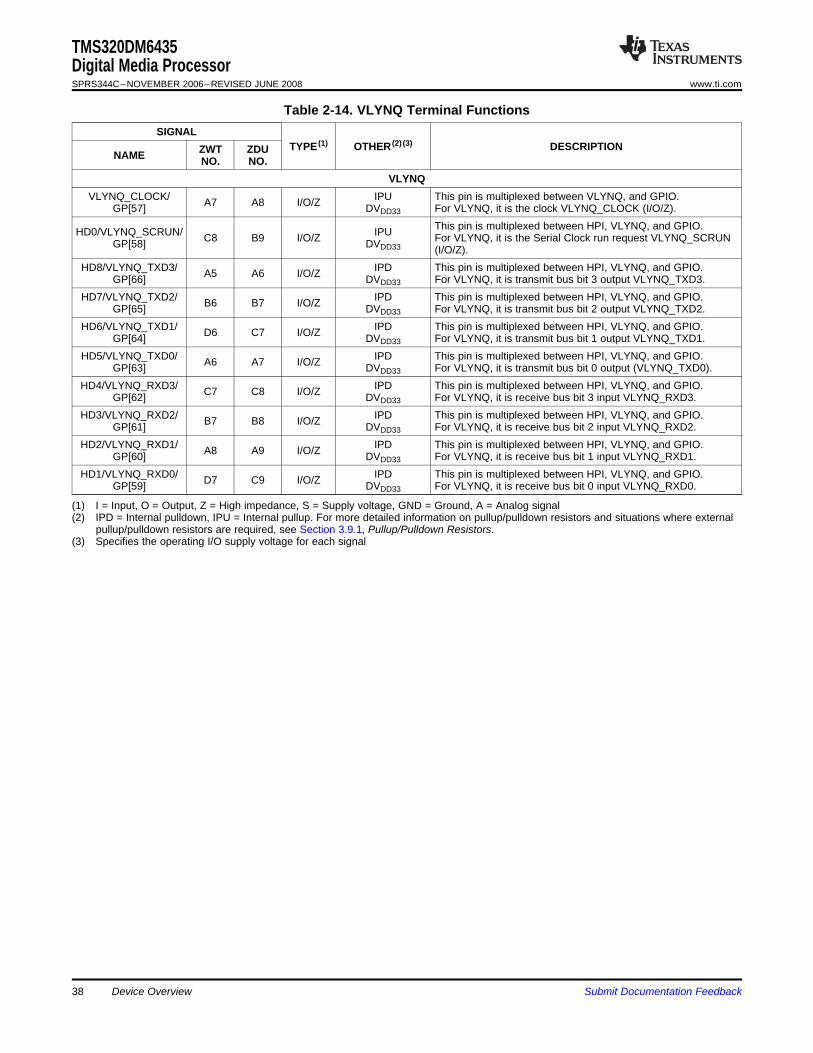
TMS320DM6435Digital Media ProcessorSPRS344C–NOVEMBER 2006–REVISED JUNE 2008 www.ti.com
Table 2-14. VLYNQ Terminal FunctionsSIGNAL
TYPE (1) OTHER (2) (3) DESCRIPTIONZWT ZDUNAME NO. NO.VLYNQ
VLYNQ_CLOCK/ IPU This pin is multiplexed between VLYNQ, and GPIO.A7 A8 I/O/ZGP[57] DVDD33 For VLYNQ, it is the clock VLYNQ_CLOCK (I/O/Z).This pin is multiplexed between HPI, VLYNQ, and GPIO.HD0/VLYNQ_SCRUN/ IPUC8 B9 I/O/Z For VLYNQ, it is the Serial Clock run request VLYNQ_SCRUNGP[58] DVDD33 (I/O/Z).
HD8/VLYNQ_TXD3/ IPD This pin is multiplexed between HPI, VLYNQ, and GPIO.A5 A6 I/O/ZGP[66] DVDD33 For VLYNQ, it is transmit bus bit 3 output VLYNQ_TXD3.HD7/VLYNQ_TXD2/ IPD This pin is multiplexed between HPI, VLYNQ, and GPIO.B6 B7 I/O/ZGP[65] DVDD33 For VLYNQ, it is transmit bus bit 2 output VLYNQ_TXD2.HD6/VLYNQ_TXD1/ IPD This pin is multiplexed between HPI, VLYNQ, and GPIO.D6 C7 I/O/ZGP[64] DVDD33 For VLYNQ, it is transmit bus bit 1 output VLYNQ_TXD1.HD5/VLYNQ_TXD0/ IPD This pin is multiplexed between HPI, VLYNQ, and GPIO.A6 A7 I/O/ZGP[63] DVDD33 For VLYNQ, it is transmit bus bit 0 output (VLYNQ_TXD0).HD4/VLYNQ_RXD3/ IPD This pin is multiplexed between HPI, VLYNQ, and GPIO.C7 C8 I/O/ZGP[62] DVDD33 For VLYNQ, it is receive bus bit 3 input VLYNQ_RXD3.HD3/VLYNQ_RXD2/ IPD This pin is multiplexed between HPI, VLYNQ, and GPIO.B7 B8 I/O/ZGP[61] DVDD33 For VLYNQ, it is receive bus bit 2 input VLYNQ_RXD2.HD2/VLYNQ_RXD1/ IPD This pin is multiplexed between HPI, VLYNQ, and GPIO.A8 A9 I/O/ZGP[60] DVDD33 For VLYNQ, it is receive bus bit 1 input VLYNQ_RXD1.HD1/VLYNQ_RXD0/ IPD This pin is multiplexed between HPI, VLYNQ, and GPIO.D7 C9 I/O/ZGP[59] DVDD33 For VLYNQ, it is receive bus bit 0 input VLYNQ_RXD0.
(1) I = Input, O = Output, Z = High impedance, S = Supply voltage, GND = Ground, A = Analog signal(2) IPD = Internal pulldown, IPU = Internal pullup. For more detailed information on pullup/pulldown resistors and situations where external
pullup/pulldown resistors are required, see Section 3.9.1, Pullup/Pulldown Resistors.(3) Specifies the operating I/O supply voltage for each signal
Device Overview38 Submit Documentation Feedback
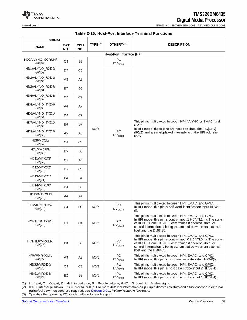
TMS320DM6435Digital Media Processor
www.ti.com SPRS344C–NOVEMBER 2006–REVISED JUNE 2008
Table 2-15. Host-Port Interface Terminal FunctionsSIGNAL
TYPE (1) OTHER (2) (3) DESCRIPTIONZWT ZDUNAME NO. NO.Host-Port Interface (HPI)
HD0/VLYNQ_SCRUN/ IPUC8 B9GP[58] DVDD33
HD1/VLYNQ_RXD0/ D7 C9GP[59]HD2/VLYNQ_RXD1/ A8 A9GP[60]HD3/VLYNQ_RXD2/ B7 B8GP[61]HD4/VLYNQ_RXD3/ C7 C8GP[62]HD5/VLYNQ_TXD0/ A6 A7GP[63]HD6/VLYNQ_TXD1/ D6 C7GP[64]
This pin is multiplexed between HPI, VLYNQ or EMAC, andHD7/VLYNQ_TXD2/ B6 B7 GPIO.GP[65]I/O/Z In HPI mode, these pins are host-port data pins HD[15:0]
HD8/VLYNQ_TXD3/ IPD (I/O/Z) and are multiplexed internally with the HPI addressA5 A6GP[66] DVDD33 lines.HD9/MCOL/ C6 C6GP[67]
HD10/MCRS/ B5 B6GP[68]HD11/MTXD3/ C5 A5GP[69]HD12/MTXD2/ D5 C5GP[70]HD13/MTXD1/ B4 B4GP[71]HD14/MTXD0/ D4 B5GP[72]
HD15/MTXCLK/ A4 A4GP[73]This pin is multiplexed between HPI, EMAC, and GPIO.HHWIL/MRXDV/ IPDC4 D3 I/O/Z In HPI mode, this pin is half-word identification input HHWILGP[74] DVDD33 (I).This pin is multiplexed between HPI, EMAC, and GPIO.In HPI mode, this pin is control input 1 HCNTL1 (I). The stateHCNTL1/MTXEN/ IPDD3 C4 I/O/Z of HCNTL1 and HCNTL0 determines if address, data, orGP[75] DVDD33 control information is being transmitted between an externalhost and the DM6435.This pin is multiplexed between HPI, EMAC, and GPIO.In HPI mode, this pin is control input 0 HCNTL0 (I). The stateHCNTL0/MRXER/ IPDB3 B2 I/O/Z of HCNTL1 and HCNTL0 determines if address, data, orGP[76] DVDD33 control information is being transmitted between an externalhost and the DM6435.
HR/W/MRXCLK/ IPD This pin is multiplexed between HPI, EMAC, and GPIO.A3 A3 I/O/ZGP[77] DVDD33 In HPI mode, this pin is host read or write select HR/W(I).HDS2/MRXD0/ IPU This pin is multiplexed between HPI, EMAC, and GPIO.C3 C2 I/O/ZGP[78] DVDD33 In HPI mode, this pin is host data strobe input 2 HDS2 (I).HDS1/MRXD1/ IPU This pin is multiplexed between HPI, EMAC, and GPIO.B2 B3 I/O/ZGP[79] DVDD33 In HPI mode, this pin is host data strobe input 1 HDS1 (I).
(1) I = Input, O = Output, Z = High impedance, S = Supply voltage, GND = Ground, A = Analog signal(2) IPD = Internal pulldown, IPU = Internal pullup. For more detailed information on pullup/pulldown resistors and situations where external
pullup/pulldown resistors are required, see Section 3.9.1, Pullup/Pulldown Resistors.(3) Specifies the operating I/O supply voltage for each signal
Submit Documentation Feedback Device Overview 39
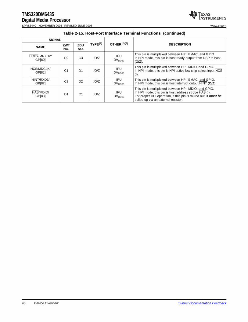
TMS320DM6435Digital Media ProcessorSPRS344C–NOVEMBER 2006–REVISED JUNE 2008 www.ti.com
Table 2-15. Host-Port Interface Terminal Functions (continued)SIGNAL
TYPE (1) OTHER (2) (3) DESCRIPTIONZWT ZDUNAME NO. NO.This pin is multiplexed between HPI, EMAC, and GPIO.HRDY/MRXD2/ IPUD2 C3 I/O/Z In HPI mode, this pin is host ready output from DSP to hostGP[80] DVDD33 (O/Z).This pin is multiplexed between HPI, MDIO, and GPIO.HCS/MDCLK/ IPUC1 D1 I/O/Z In HPI mode, this pin is HPI active low chip select input HCSGP[81] DVDD33 (I).
HINT/RXD3/ IPU This pin is multiplexed between HPI, EMAC, and GPIO.C2 D2 I/O/ZGP[82] DVDD33 In HPI mode, this pin is host interrupt output HINT (O/Z).This pin is multiplexed between HPI, MDIO, and GPIO.
HAS/MDIO/ IPU In HPI mode, this pin is host address strobe HAS (I).D1 C1 I/O/ZGP[83] DVDD33 For proper HPI operation, if this pin is routed out, it must bepulled up via an external resistor.
Device Overview40 Submit Documentation Feedback
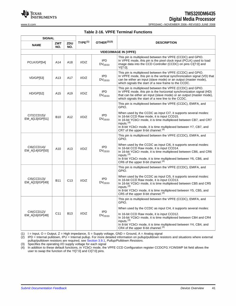
TMS320DM6435Digital Media Processor
www.ti.com SPRS344C–NOVEMBER 2006–REVISED JUNE 2008
Table 2-16. VPFE Terminal FunctionsSIGNAL
TYPE (1) OTHER (2) (3) DESCRIPTIONZWT ZDUNAME NO. NO.VIDEO/IMAGE IN (VPFE)
This pin is multiplexed between the VPFE (CCDC) and GPIO.IPD In VPFE mode, this pin is the pixel clock input (PCLK) used to loadPCLK/GP[54] A14 A18 I/O/Z DVDD33 image data into the CCD Controller (CCDC) on pins CI[7:0] and
YI[7:0].This pin is multiplexed between the VPFE (CCDC) and GPIO.
IPD In VPFE mode, this pin is the vertical synchronization signal (VD) thatVD/GP[53] A13 A17 I/O/Z DVDD33 can be either an input (slave mode) or an output (master mode),which signals the start of a new frame to the CCDC.This pin is multiplexed between the VPFE (CCDC) and GPIO.
IPD In VPFE mode, this pin is the horizontal synchronization signal (HD)HD/GP[52] A15 A19 I/O/Z DVDD33 that can be either an input (slave mode) or an output (master mode),which signals the start of a new line to the CCDC.This pin is multiplexed between the VPFE (CCDC), EMIFA, andGPIO.
When used by the CCDC as input CI7, it supports several modes:CI7(CCD15)/ IPD In 16-bit CCD Raw mode, it is input CCD15.B10 A12 I/O/ZEM_A[13]/GP[51] DVDD33 In 16-bit YCbCr mode, it is time multiplexed between CB7, and CR7
inputs. (4)
In 8-bit YCbCr mode, it is time multiplexed between Y7, CB7, andCR7 of the upper 8-bit channel. (4)
This pin is multiplexed between the VPFE (CCDC), EMIFA, andGPIO.
When used by the CCDC as input CI6, it supports several modes:CI6(CCD14)/ IPD In 16-bit CCD Raw mode, it is input CCD14.A10 A13 I/O/ZEM_A[14]/GP[50] DVDD33 In 16-bit YCbCr mode, it is time multiplexed between CB6, and CR6
inputs. (4)
In 8-bit YCbCr mode, it is time multiplexed between Y6, CB6, andCR6 of the upper 8-bit channel. (4)
This pin is multiplexed between the VPFE (CCDC), EMIFA, andGPIO.
When used by the CCDC as input CI5, it supports several modes:CI5(CCD13)/ IPD In 16-bit CCD Raw mode, it is input CCD13.B11 C13 I/O/ZEM_A[15]/GP[49] DVDD33 In 16-bit YCbCr mode, it is time multiplexed between CB5 and CR5
inputs. (4)
In 8-bit YCbCr mode, it is time multiplexed between Y5, CB5, andCR5 of the upper 8-bit channel. (4)
This pin is multiplexed between the VPFE (CCDC), EMIFA, andGPIO.
When used by the CCDC as input CI4, it supports several modes:CI4(CCD12)/ IPDC11 B13 I/O/Z In 16-bit CCD Raw mode, it is input CCD12.EM_A[16]/GP[48] DVDD33 In 16-bit YCbCr mode, it is time multiplexed between CB4 and CR4
inputs. (4)
In 8-bit YCbCr mode, it is time multiplexed between Y4, CB4, andCR4 of the upper 8-bit channel. (4)
(1) I = Input, O = Output, Z = High impedance, S = Supply voltage, GND = Ground, A = Analog signal(2) IPD = Internal pulldown, IPU = Internal pullup. For more detailed information on pullup/pulldown resistors and situations where external
pullup/pulldown resistors are required, see Section 3.9.1, Pullup/Pulldown Resistors.(3) Specifies the operating I/O supply voltage for each signal(4) In addition to these default functions, in YCbCr mode, the VPFE CCD Configuration register CCDCFG.YCINSWP bit field allows the
user to swap the function of the YI[7:0] and CI[7:0] pins.
Submit Documentation Feedback Device Overview 41
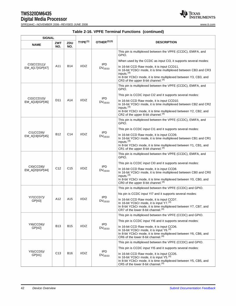
TMS320DM6435Digital Media ProcessorSPRS344C–NOVEMBER 2006–REVISED JUNE 2008 www.ti.com
Table 2-16. VPFE Terminal Functions (continued)SIGNAL
TYPE (1) OTHER (2) (3) DESCRIPTIONZWT ZDUNAME NO. NO.This pin is multiplexed between the VPFE (CCDC), EMIFA, andGPIO.
When used by the CCDC as input CI3, it supports several modes:CI3(CCD11)/ IPDA11 B14 I/O/Z In 16-bit CCD Raw mode, it is input CCD11.EM_A[17]/GP[47] DVDD33 In 16-bit YCbCr mode, it is time multiplexed between CB3 and CR3
inputs. (4)
In 8-bit YCbCr mode, it is time multiplexed between Y3, CB3, andCR3 of the upper 8-bit channel. (4)
This pin is multiplexed between the VPFE (CCDC), EMIFA, andGPIO.
This pin is CCDC input CI2 and it supports several modes:CI2(CCD10)/ IPDD11 A14 I/O/Z In 16-bit CCD Raw mode, it is input CCD10.EM_A[18]/GP[46] DVDD33 In 16-bit YCbCr mode, it is time multiplexed between CB2 and CR2
inputs. (4)
In 8-bit YCbCr mode, it is time multiplexed between Y2, CB2, andCR2 of the upper 8-bit channel. (4)
This pin is multiplexed between the VPFE (CCDC), EMIFA, andGPIO.
This pin is CCDC input CI1 and it supports several modes:CI1(CCD9)/ IPDB12 C14 I/O/Z In 16-bit CCD Raw mode, it is input CCD9.EM_A[19]/GP[45] DVDD33 In 16-bit YCbCr mode, it is time multiplexed between CB1 and CR1
inputs. (4)
In 8-bit YCbCr mode, it is time multiplexed between Y1, CB1, andCR1 of the upper 8-bit channel. (4)
This pin is multiplexed between the VPFE (CCDC), EMIFA, andGPIO.
This pin is CCDC input CI0 and it supports several modes:CI0(CCD8)/ IPDC12 C15 I/O/Z In 16-bit CCD Raw mode, it is input CCD8.EM_A[20]/GP[44] DVDD33 In 16-bit YCbCr mode, it is time multiplexed between CB0 and CR0
inputs. (4)
In 8-bit YCbCr mode, it is time multiplexed between Y0, CB0, andCR0 of the upper 8-bit channel. (4)
This pin is multiplexed between the VPFE (CCDC) and GPIO.
his pin is CCDC input YI7 and it supports several modes:YI7(CCD7)/ IPDA12 A15 I/O/Z In 16-bit CCD Raw mode, it is input CCD7.GP[43] DVDD33 In 16-bit YCbCr mode, it is input Y7. (4)
In 8-bit YCbCr mode, it is time multiplexed between Y7, CB7, andCR7 of the lower 8-bit channel. (4)
This pin is multiplexed between the VPFE (CCDC) and GPIO.
This pin is CCDC input YI6 and it supports several modes:YI6(CCD6)/ IPDB13 B15 I/O/Z In 16-bit CCD Raw mode, it is input CCD6.GP[42] DVDD33 In 16-bit YCbCr mode, it is input Y6. (4)
In 8-bit YCbCr mode, it is time multiplexed between Y6, CB6, andCR6 of the lower 8-bit channel. (4)
This pin is multiplexed between the VPFE (CCDC) and GPIO.
This pin is CCDC input YI5 and it supports several modes:YI5(CCD5)/ IPDC13 B16 I/O/Z In 16-bit CCD Raw mode, it is input CCD5.GP[41] DVDD33 In 16-bit YCbCr mode, it is input Y5. (4)
In 8-bit YCbCr mode, it is time multiplexed between Y5, CB5, andCR5 of the lower 8-bit channel. (4)
Device Overview42 Submit Documentation Feedback
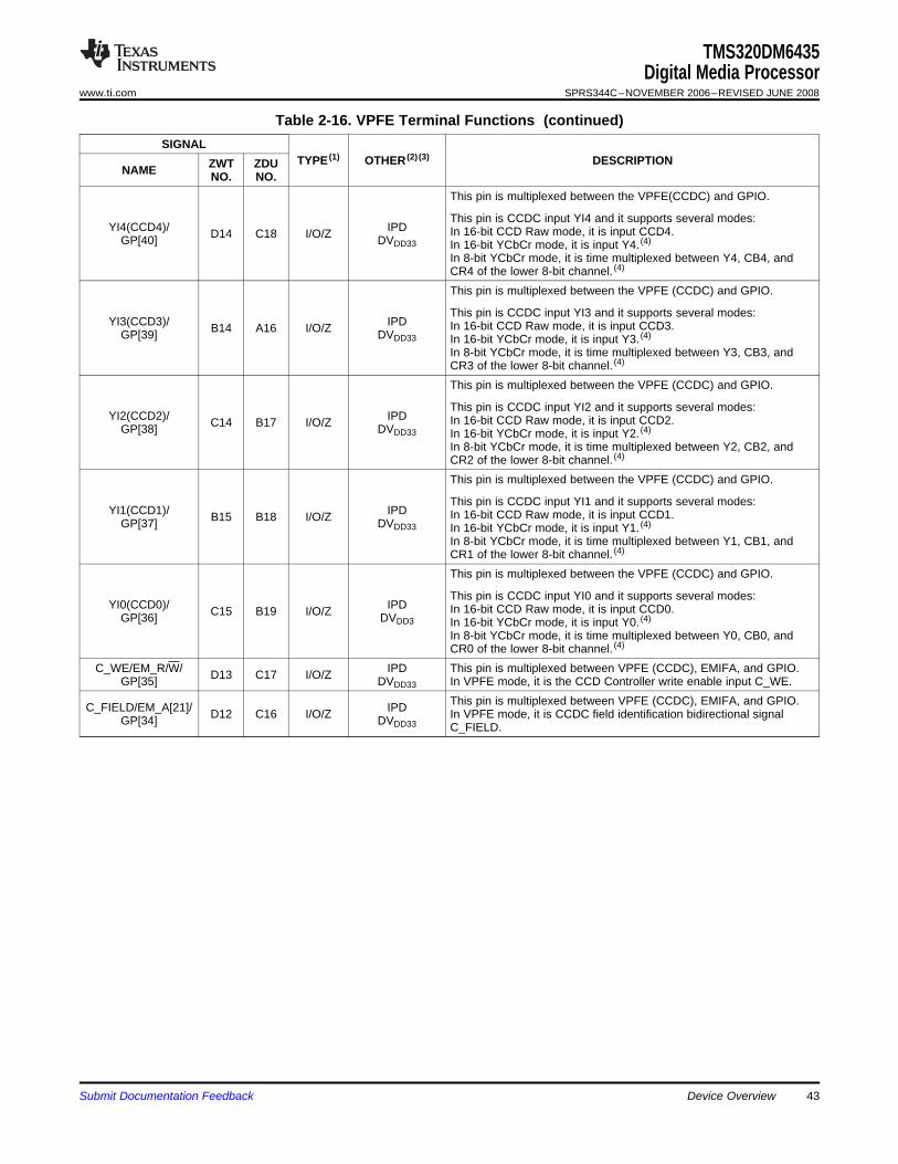
TMS320DM6435Digital Media Processor
www.ti.com SPRS344C–NOVEMBER 2006–REVISED JUNE 2008
Table 2-16. VPFE Terminal Functions (continued)SIGNAL
TYPE (1) OTHER (2) (3) DESCRIPTIONZWT ZDUNAME NO. NO.This pin is multiplexed between the VPFE(CCDC) and GPIO.
This pin is CCDC input YI4 and it supports several modes:YI4(CCD4)/ IPD In 16-bit CCD Raw mode, it is input CCD4.D14 C18 I/O/ZGP[40] DVDD33 In 16-bit YCbCr mode, it is input Y4. (4)
In 8-bit YCbCr mode, it is time multiplexed between Y4, CB4, andCR4 of the lower 8-bit channel. (4)
This pin is multiplexed between the VPFE (CCDC) and GPIO.
This pin is CCDC input YI3 and it supports several modes:YI3(CCD3)/ IPD In 16-bit CCD Raw mode, it is input CCD3.B14 A16 I/O/ZGP[39] DVDD33 In 16-bit YCbCr mode, it is input Y3. (4)
In 8-bit YCbCr mode, it is time multiplexed between Y3, CB3, andCR3 of the lower 8-bit channel. (4)
This pin is multiplexed between the VPFE (CCDC) and GPIO.
This pin is CCDC input YI2 and it supports several modes:YI2(CCD2)/ IPD In 16-bit CCD Raw mode, it is input CCD2.C14 B17 I/O/ZGP[38] DVDD33 In 16-bit YCbCr mode, it is input Y2. (4)
In 8-bit YCbCr mode, it is time multiplexed between Y2, CB2, andCR2 of the lower 8-bit channel. (4)
This pin is multiplexed between the VPFE (CCDC) and GPIO.
This pin is CCDC input YI1 and it supports several modes:YI1(CCD1)/ IPD In 16-bit CCD Raw mode, it is input CCD1.B15 B18 I/O/ZGP[37] DVDD33 In 16-bit YCbCr mode, it is input Y1. (4)
In 8-bit YCbCr mode, it is time multiplexed between Y1, CB1, andCR1 of the lower 8-bit channel. (4)
This pin is multiplexed between the VPFE (CCDC) and GPIO.
This pin is CCDC input YI0 and it supports several modes:YI0(CCD0)/ IPD In 16-bit CCD Raw mode, it is input CCD0.C15 B19 I/O/ZGP[36] DVDD3 In 16-bit YCbCr mode, it is input Y0. (4)
In 8-bit YCbCr mode, it is time multiplexed between Y0, CB0, andCR0 of the lower 8-bit channel. (4)
C_WE/EM_R/W/ IPD This pin is multiplexed between VPFE (CCDC), EMIFA, and GPIO.D13 C17 I/O/ZGP[35] DVDD33 In VPFE mode, it is the CCD Controller write enable input C_WE.This pin is multiplexed between VPFE (CCDC), EMIFA, and GPIO.C_FIELD/EM_A[21]/ IPDD12 C16 I/O/Z In VPFE mode, it is CCDC field identification bidirectional signalGP[34] DVDD33 C_FIELD.
Submit Documentation Feedback Device Overview 43
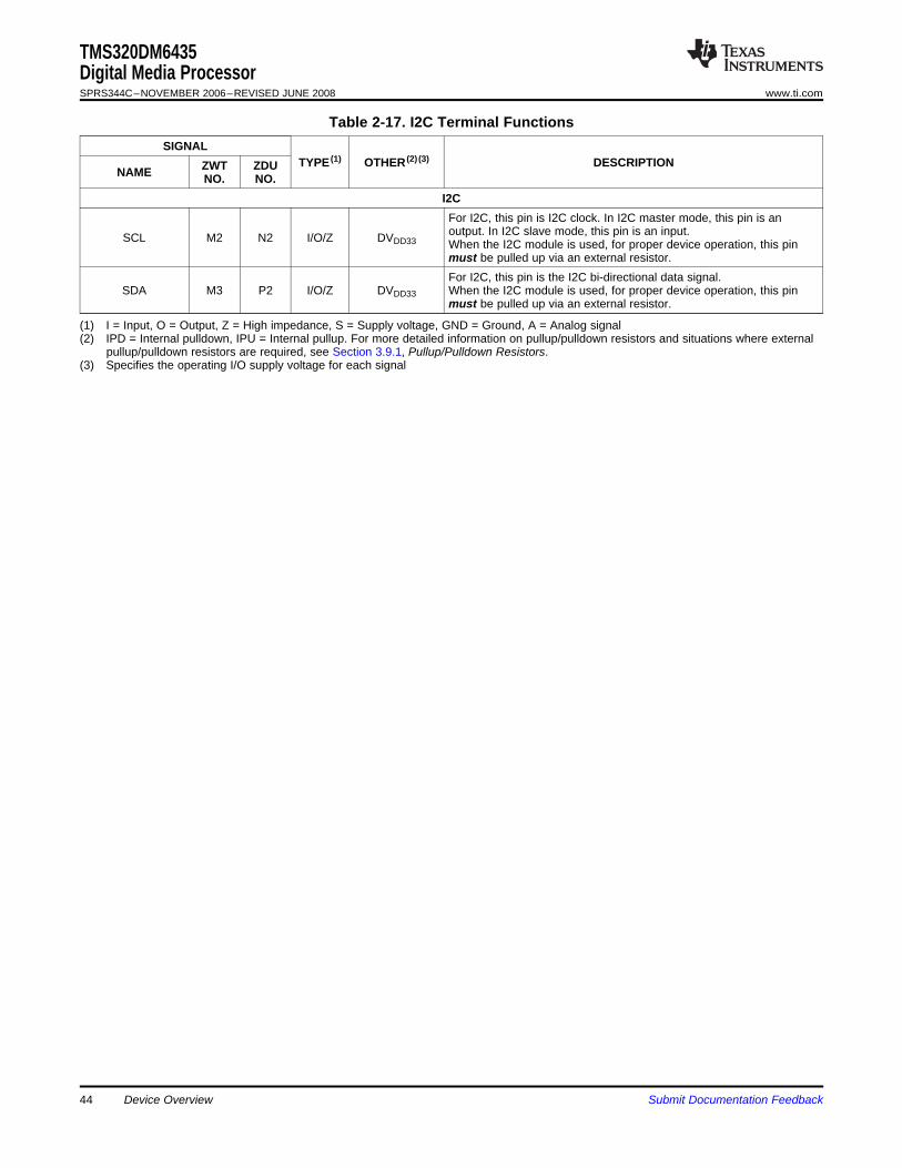
TMS320DM6435Digital Media ProcessorSPRS344C–NOVEMBER 2006–REVISED JUNE 2008 www.ti.com
Table 2-17. I2C Terminal FunctionsSIGNAL
TYPE (1) OTHER (2) (3) DESCRIPTIONZWT ZDUNAME NO. NO.I2CFor I2C, this pin is I2C clock. In I2C master mode, this pin is anoutput. In I2C slave mode, this pin is an input.SCL M2 N2 I/O/Z DVDD33 When the I2C module is used, for proper device operation, this pinmust be pulled up via an external resistor.For I2C, this pin is the I2C bi-directional data signal.
SDA M3 P2 I/O/Z DVDD33 When the I2C module is used, for proper device operation, this pinmust be pulled up via an external resistor.
(1) I = Input, O = Output, Z = High impedance, S = Supply voltage, GND = Ground, A = Analog signal(2) IPD = Internal pulldown, IPU = Internal pullup. For more detailed information on pullup/pulldown resistors and situations where external
pullup/pulldown resistors are required, see Section 3.9.1, Pullup/Pulldown Resistors.(3) Specifies the operating I/O supply voltage for each signal
Device Overview44 Submit Documentation Feedback
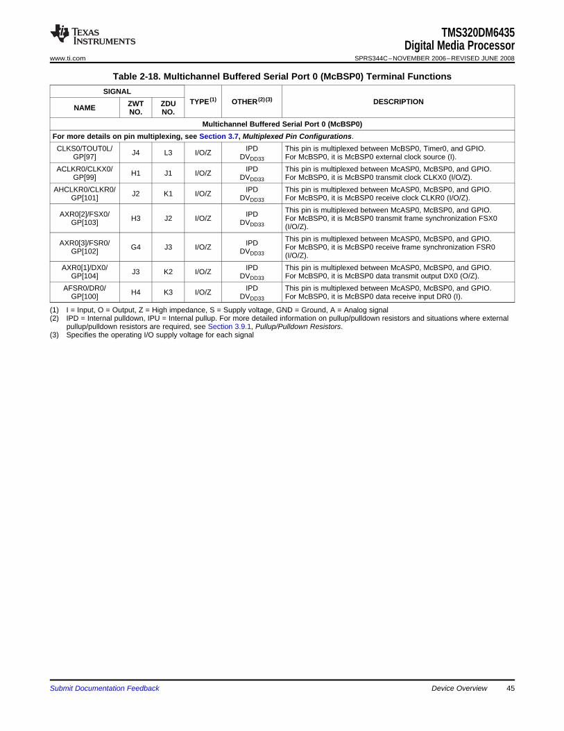
TMS320DM6435Digital Media Processor
www.ti.com SPRS344C–NOVEMBER 2006–REVISED JUNE 2008
Table 2-18. Multichannel Buffered Serial Port 0 (McBSP0) Terminal FunctionsSIGNAL
TYPE (1) OTHER (2) (3) DESCRIPTIONZWT ZDUNAME NO. NO.Multichannel Buffered Serial Port 0 (McBSP0)
For more details on pin multiplexing, see Section 3.7, Multiplexed Pin Configurations.CLKS0/TOUT0L/ IPD This pin is multiplexed between McBSP0, Timer0, and GPIO.J4 L3 I/O/ZGP[97] DVDD33 For McBSP0, it is McBSP0 external clock source (I).ACLKR0/CLKX0/ IPD This pin is multiplexed between McASP0, McBSP0, and GPIO.H1 J1 I/O/ZGP[99] DVDD33 For McBSP0, it is McBSP0 transmit clock CLKX0 (I/O/Z).
AHCLKR0/CLKR0/ IPD This pin is multiplexed between McASP0, McBSP0, and GPIO.J2 K1 I/O/ZGP[101] DVDD33 For McBSP0, it is McBSP0 receive clock CLKR0 (I/O/Z).This pin is multiplexed between McASP0, McBSP0, and GPIO.AXR0[2]/FSX0/ IPDH3 J2 I/O/Z For McBSP0, it is McBSP0 transmit frame synchronization FSX0GP[103] DVDD33 (I/O/Z).This pin is multiplexed between McASP0, McBSP0, and GPIO.AXR0[3]/FSR0/ IPDG4 J3 I/O/Z For McBSP0, it is McBSP0 receive frame synchronization FSR0GP[102] DVDD33 (I/O/Z).
AXR0[1]/DX0/ IPD This pin is multiplexed between McASP0, McBSP0, and GPIO.J3 K2 I/O/ZGP[104] DVDD33 For McBSP0, it is McBSP0 data transmit output DX0 (O/Z).AFSR0/DR0/ IPD This pin is multiplexed between McASP0, McBSP0, and GPIO.H4 K3 I/O/ZGP[100] DVDD33 For McBSP0, it is McBSP0 data receive input DR0 (I).
(1) I = Input, O = Output, Z = High impedance, S = Supply voltage, GND = Ground, A = Analog signal(2) IPD = Internal pulldown, IPU = Internal pullup. For more detailed information on pullup/pulldown resistors and situations where external
pullup/pulldown resistors are required, see Section 3.9.1, Pullup/Pulldown Resistors.(3) Specifies the operating I/O supply voltage for each signal
Submit Documentation Feedback Device Overview 45
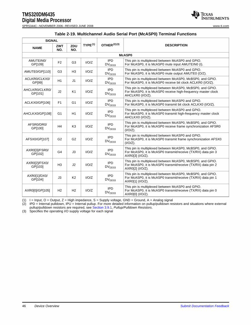
TMS320DM6435Digital Media ProcessorSPRS344C–NOVEMBER 2006–REVISED JUNE 2008 www.ti.com
Table 2-19. Multichannel Audio Serial Port (McASP0) Terminal FunctionsSIGNAL
TYPE (1) OTHER (2) (3) DESCRIPTIONZWT ZDUNAME NO. NO.McASP0
AMUTEIN0/ IPD This pin is multiplexed between McASP0 and GPIO.F2 G3 I/O/ZGP[109] DVDD33 For McASP0, it is McASP0 mute input AMUTEIN0 (I).IPD This pin is multiplexed between McASP0 and GPIO.AMUTE0/GP[110] G3 H3 I/O/Z DVDD33 For McASP0, it is McASP0 mute output AMUTE0 (O/Z).
ACLKR0/CLKX0/ IPD This pin is multiplexed between McASP0, McBSP0, and GPIO.H1 J1 I/O/ZGP[99] DVDD33 For McASP0, it is McASP0 receive bit clock ACLKR0 (I/O/Z).This pin is multiplexed between McASP0, McBSP0, and GPIO.AHCLKR0/CLKR0/ IPDJ2 K1 I/O/Z For McASP0, it is McASP0 receive high-frequency master clockGP[101] DVDD33 AHCLKR0 (I/O/Z).
IPD This pin is multiplexed between McASP0 and GPIO.ACLKX0/GP[106] F1 G1 I/O/Z DVDD33 For McASP0, it is McASP0 transmit bit clock ACLKX0 (I/O/Z).This pin is multiplexed between McASP0 and GPIO.IPDAHCLKX0/GP[108] G1 H1 I/O/Z For McASP0, it is McASP0 transmit high-frequency master clockDVDD33 AHCLKX0 (I/O/Z).This pin is multiplexed between McASP0, McBSP0, and GPIO.AFSR0/DR0/ IPDH4 K3 I/O/Z For McASP0, it is McASP0 receive frame synchronization AFSR0GP[100] DVDD33 (I/O/Z).This pin is multiplexed between McASP0 and GPIO.IPDAFSX0/GP[107] G2 G2 I/O/Z For McASP0, it is McASP0 transmit frame synchronization AFSX0DVDD33 (I/O/Z).This pin is multiplexed between McASP0, McBSP0, and GPIO.AXR0[3]/FSR0/ IPDG4 J3 I/O/Z For McASP0, it is McASP0 transmit/receive (TX/RX) data pin 3GP[102] DVDD33 AXR0[3] (I/O/Z).This pin is multiplexed between McASP0, McBSP0, and GPIO.AXR0[2]/FSX0/ IPDH3 J2 I/O/Z For McASP0, it is McASP0 transmit/receive (TX/RX) data pin 2GP[103] DVDD33 AXR0[2] (I/O/Z).This pin is multiplexed between McASP0, McBSP0, and GPIO.AXR0[1]/DX0/ IPDJ3 K2 I/O/Z For McASP0, it is McASP0 transmit/receive (TX/RX) data pin 1GP[104] DVDD33 AXR0[1] (I/O/Z).This pin is multiplexed between McASP0 and GPIO.IPDAXR0[0]/GP[105] H2 H2 I/O/Z For McASP0, it is McASP0 transmit/receive (TX/RX) data pin 0DVDD33 AXR0[0] (I/O/Z).
(1) I = Input, O = Output, Z = High impedance, S = Supply voltage, GND = Ground, A = Analog signal(2) IPD = Internal pulldown, IPU = Internal pullup. For more detailed information on pullup/pulldown resistors and situations where external
pullup/pulldown resistors are required, see Section 3.9.1, Pullup/Pulldown Resistors.(3) Specifies the operating I/O supply voltage for each signal
Device Overview46 Submit Documentation Feedback
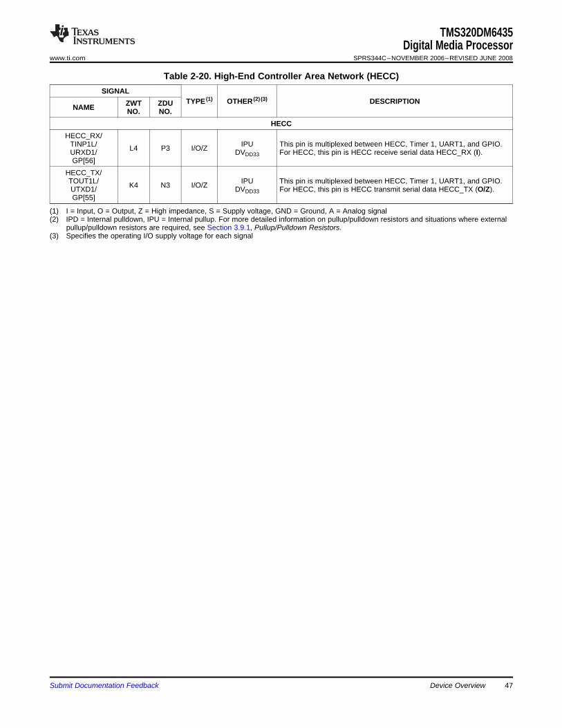
TMS320DM6435Digital Media Processor
www.ti.com SPRS344C–NOVEMBER 2006–REVISED JUNE 2008
Table 2-20. High-End Controller Area Network (HECC)SIGNAL
TYPE (1) OTHER (2) (3) DESCRIPTIONZWT ZDUNAME NO. NO.HECC
HECC_RX/TINP1L/ IPU This pin is multiplexed between HECC, Timer 1, UART1, and GPIO.L4 P3 I/O/ZURXD1/ DVDD33 For HECC, this pin is HECC receive serial data HECC_RX (I).GP[56]
HECC_TX/TOUT1L/ IPU This pin is multiplexed between HECC, Timer 1, UART1, and GPIO.K4 N3 I/O/ZUTXD1/ DVDD33 For HECC, this pin is HECC transmit serial data HECC_TX (O/Z).GP[55]
(1) I = Input, O = Output, Z = High impedance, S = Supply voltage, GND = Ground, A = Analog signal(2) IPD = Internal pulldown, IPU = Internal pullup. For more detailed information on pullup/pulldown resistors and situations where external
pullup/pulldown resistors are required, see Section 3.9.1, Pullup/Pulldown Resistors.(3) Specifies the operating I/O supply voltage for each signal
Submit Documentation Feedback Device Overview 47
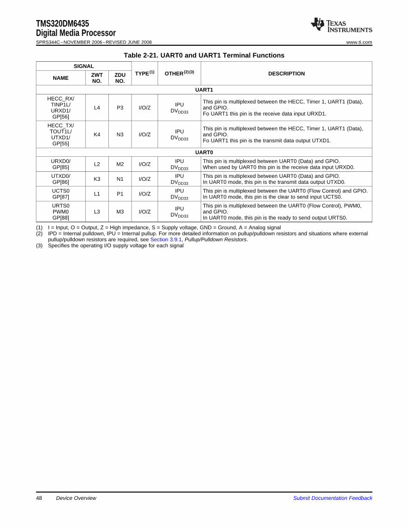
TMS320DM6435Digital Media ProcessorSPRS344C–NOVEMBER 2006–REVISED JUNE 2008 www.ti.com
Table 2-21. UART0 and UART1 Terminal FunctionsSIGNAL
TYPE (1) OTHER (2) (3) DESCRIPTIONZWT ZDUNAME NO. NO.UART1
HECC_RX/ This pin is multiplexed between the HECC, Timer 1, UART1 (Data),TINP1L/ IPUL4 P3 I/O/Z and GPIO.URXD1/ DVDD33 Fo UART1 this pin is the receive data input URXD1.GP[56]HECC_TX/ This pin is multiplexed between the HECC, Timer 1, UART1 (Data),TOUT1L/ IPUK4 N3 I/O/Z and GPIO.UTXD1/ DVDD33 Fo UART1 this pin is the transmit data output UTXD1.GP[55]
UART0URXD0/ IPU This pin is multiplexed between UART0 (Data) and GPIO.L2 M2 I/O/ZGP[85] DVDD33 When used by UART0 this pin is the receive data input URXD0.UTXD0/ IPU This pin is multiplexed between UART0 (Data) and GPIO.K3 N1 I/O/ZGP[86] DVDD33 In UART0 mode, this pin is the transmit data output UTXD0.UCTS0 IPU This pin is multiplexed between the UART0 (Flow Control) and GPIO.L1 P1 I/O/ZGP[87] DVDD33 In UART0 mode, this pin is the clear to send input UCTS0.URTS0 This pin is multiplexed between the UART0 (Flow Control), PWM0,IPUPWM0 L3 M3 I/O/Z and GPIO.DVDD33GP[88] In UART0 mode, this pin is the ready to send output URTS0.
(1) I = Input, O = Output, Z = High impedance, S = Supply voltage, GND = Ground, A = Analog signal(2) IPD = Internal pulldown, IPU = Internal pullup. For more detailed information on pullup/pulldown resistors and situations where external
pullup/pulldown resistors are required, see Section 3.9.1, Pullup/Pulldown Resistors.(3) Specifies the operating I/O supply voltage for each signal
Device Overview48 Submit Documentation Feedback
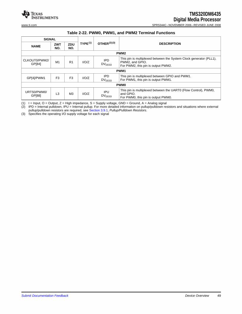
TMS320DM6435Digital Media Processor
www.ti.com SPRS344C–NOVEMBER 2006–REVISED JUNE 2008
Table 2-22. PWM0, PWM1, and PWM2 Terminal FunctionsSIGNAL
TYPE (1) OTHER (2) (3) DESCRIPTIONZWT ZDUNAME NO. NO.PWM2
This pin is multiplexed between the System Clock generator (PLL1),CLKOUT0/PWM2/ IPDM1 R1 I/O/Z PWM2, and GPIO.GP[84] DVDD33 For PWM2, this pin is output PWM2.PWM1
IPD This pin is multiplexed between GPIO and PWM1.GP[4]/PWM1 F3 F3 I/O/Z DVDD33 For PWM1, this pin is output PWM1.PWM0
This pin is multiplexed between the UART0 (Flow Control), PWM0,URTS0/PWM0/ IPUL3 M3 I/O/Z and GPIO.GP[88] DVDD33 For PWM0, this pin is output PWM0.
(1) I = Input, O = Output, Z = High impedance, S = Supply voltage, GND = Ground, A = Analog signal(2) IPD = Internal pulldown, IPU = Internal pullup. For more detailed information on pullup/pulldown resistors and situations where external
pullup/pulldown resistors are required, see Section 3.9.1, Pullup/Pulldown Resistors.(3) Specifies the operating I/O supply voltage for each signal
Submit Documentation Feedback Device Overview 49
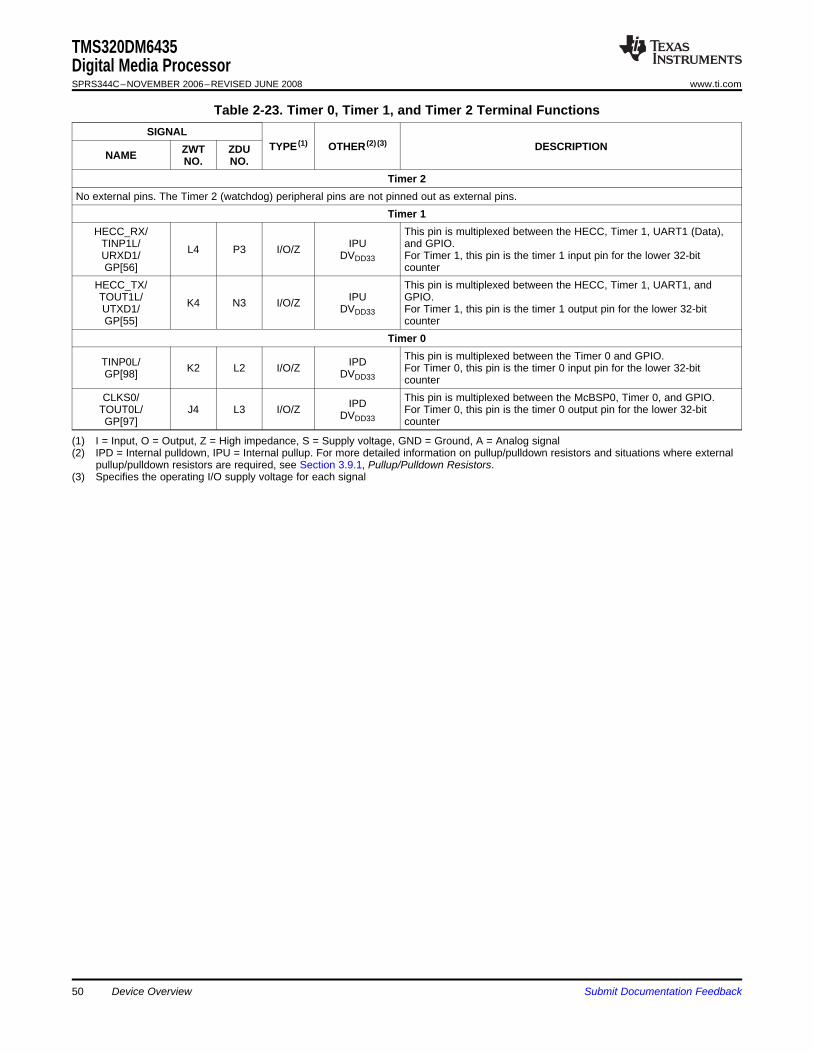
TMS320DM6435Digital Media ProcessorSPRS344C–NOVEMBER 2006–REVISED JUNE 2008 www.ti.com
Table 2-23. Timer 0, Timer 1, and Timer 2 Terminal FunctionsSIGNAL
TYPE (1) OTHER (2) (3) DESCRIPTIONZWT ZDUNAME NO. NO.Timer 2
No external pins. The Timer 2 (watchdog) peripheral pins are not pinned out as external pins.Timer 1
HECC_RX/ This pin is multiplexed between the HECC, Timer 1, UART1 (Data),TINP1L/ IPU and GPIO.L4 P3 I/O/ZURXD1/ DVDD33 For Timer 1, this pin is the timer 1 input pin for the lower 32-bitGP[56] counter
HECC_TX/ This pin is multiplexed between the HECC, Timer 1, UART1, andTOUT1L/ IPU GPIO.K4 N3 I/O/ZUTXD1/ DVDD33 For Timer 1, this pin is the timer 1 output pin for the lower 32-bitGP[55] counter
Timer 0This pin is multiplexed between the Timer 0 and GPIO.TINP0L/ IPDK2 L2 I/O/Z For Timer 0, this pin is the timer 0 input pin for the lower 32-bitGP[98] DVDD33 counter
CLKS0/ This pin is multiplexed between the McBSP0, Timer 0, and GPIO.IPDTOUT0L/ J4 L3 I/O/Z For Timer 0, this pin is the timer 0 output pin for the lower 32-bitDVDD33GP[97] counter
(1) I = Input, O = Output, Z = High impedance, S = Supply voltage, GND = Ground, A = Analog signal(2) IPD = Internal pulldown, IPU = Internal pullup. For more detailed information on pullup/pulldown resistors and situations where external
pullup/pulldown resistors are required, see Section 3.9.1, Pullup/Pulldown Resistors.(3) Specifies the operating I/O supply voltage for each signal
Device Overview50 Submit Documentation Feedback
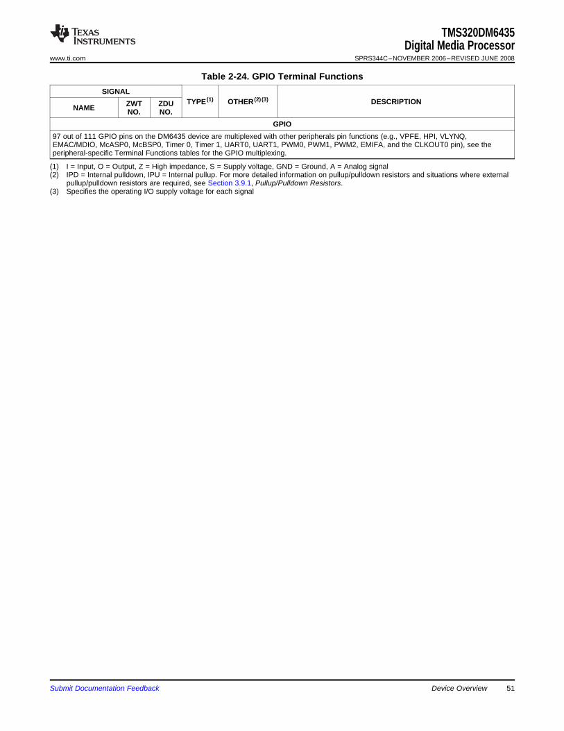
TMS320DM6435Digital Media Processor
www.ti.com SPRS344C–NOVEMBER 2006–REVISED JUNE 2008
Table 2-24. GPIO Terminal FunctionsSIGNAL
TYPE (1) OTHER (2) (3) DESCRIPTIONZWT ZDUNAME NO. NO.GPIO
97 out of 111 GPIO pins on the DM6435 device are multiplexed with other peripherals pin functions (e.g., VPFE, HPI, VLYNQ,EMAC/MDIO, McASP0, McBSP0, Timer 0, Timer 1, UART0, UART1, PWM0, PWM1, PWM2, EMIFA, and the CLKOUT0 pin), see theperipheral-specific Terminal Functions tables for the GPIO multiplexing.
(1) I = Input, O = Output, Z = High impedance, S = Supply voltage, GND = Ground, A = Analog signal(2) IPD = Internal pulldown, IPU = Internal pullup. For more detailed information on pullup/pulldown resistors and situations where external
pullup/pulldown resistors are required, see Section 3.9.1, Pullup/Pulldown Resistors.(3) Specifies the operating I/O supply voltage for each signal
Submit Documentation Feedback Device Overview 51
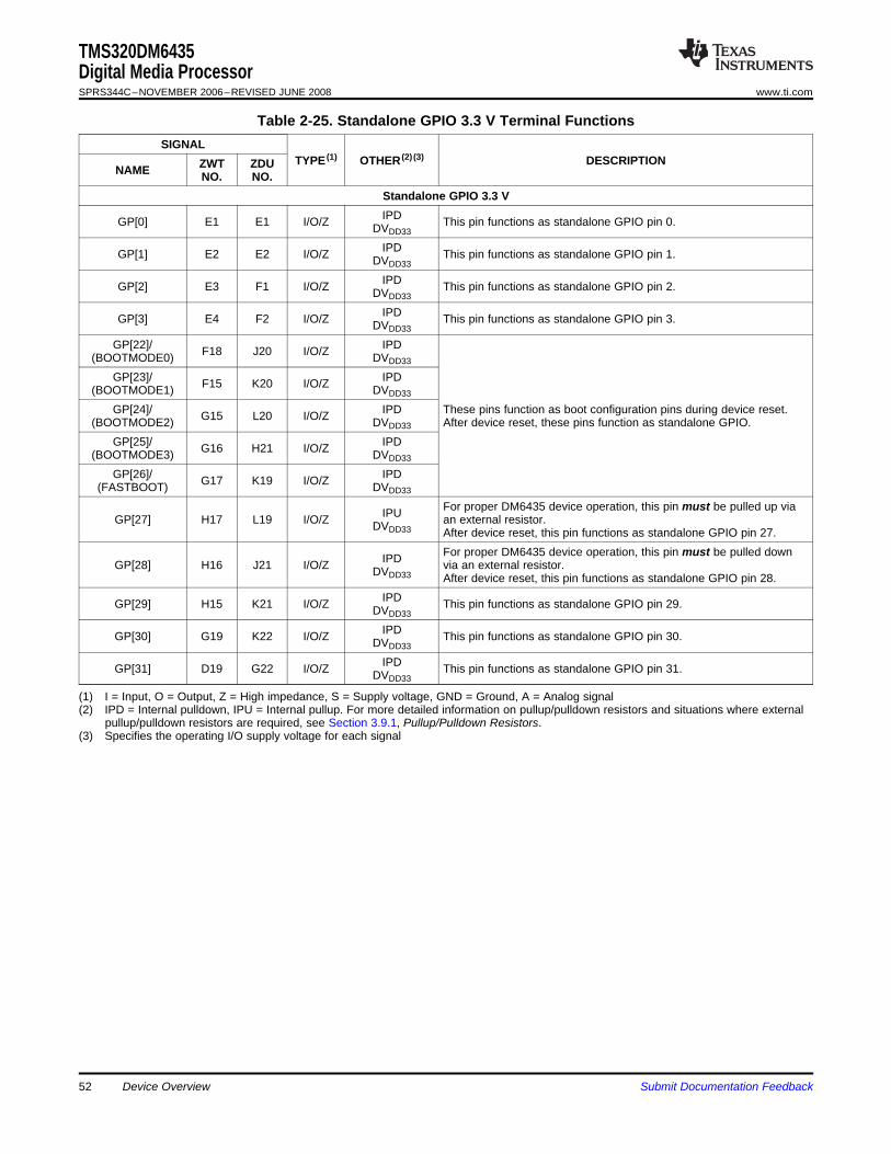
TMS320DM6435Digital Media ProcessorSPRS344C–NOVEMBER 2006–REVISED JUNE 2008 www.ti.com
Table 2-25. Standalone GPIO 3.3 V Terminal FunctionsSIGNAL
TYPE (1) OTHER (2) (3) DESCRIPTIONZWT ZDUNAME NO. NO.Standalone GPIO 3.3 VIPDGP[0] E1 E1 I/O/Z This pin functions as standalone GPIO pin 0.DVDD33
IPDGP[1] E2 E2 I/O/Z This pin functions as standalone GPIO pin 1.DVDD33
IPDGP[2] E3 F1 I/O/Z This pin functions as standalone GPIO pin 2.DVDD33
IPDGP[3] E4 F2 I/O/Z This pin functions as standalone GPIO pin 3.DVDD33
GP[22]/ IPDF18 J20 I/O/Z(BOOTMODE0) DVDD33
GP[23]/ IPDF15 K20 I/O/Z(BOOTMODE1) DVDD33
GP[24]/ IPD These pins function as boot configuration pins during device reset.G15 L20 I/O/Z(BOOTMODE2) DVDD33 After device reset, these pins function as standalone GPIO.GP[25]/ IPDG16 H21 I/O/Z(BOOTMODE3) DVDD33
GP[26]/ IPDG17 K19 I/O/Z(FASTBOOT) DVDD33
For proper DM6435 device operation, this pin must be pulled up viaIPUGP[27] H17 L19 I/O/Z an external resistor.DVDD33 After device reset, this pin functions as standalone GPIO pin 27.For proper DM6435 device operation, this pin must be pulled downIPDGP[28] H16 J21 I/O/Z via an external resistor.DVDD33 After device reset, this pin functions as standalone GPIO pin 28.
IPDGP[29] H15 K21 I/O/Z This pin functions as standalone GPIO pin 29.DVDD33
IPDGP[30] G19 K22 I/O/Z This pin functions as standalone GPIO pin 30.DVDD33
IPDGP[31] D19 G22 I/O/Z This pin functions as standalone GPIO pin 31.DVDD33
(1) I = Input, O = Output, Z = High impedance, S = Supply voltage, GND = Ground, A = Analog signal(2) IPD = Internal pulldown, IPU = Internal pullup. For more detailed information on pullup/pulldown resistors and situations where external
pullup/pulldown resistors are required, see Section 3.9.1, Pullup/Pulldown Resistors.(3) Specifies the operating I/O supply voltage for each signal
Device Overview52 Submit Documentation Feedback
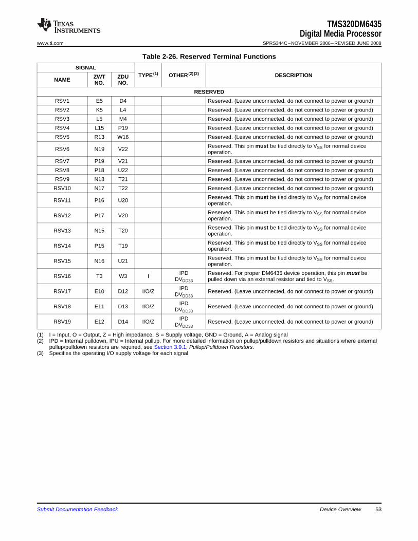
TMS320DM6435Digital Media Processor
www.ti.com SPRS344C–NOVEMBER 2006–REVISED JUNE 2008
Table 2-26. Reserved Terminal FunctionsSIGNAL
TYPE (1) OTHER (2) (3) DESCRIPTIONZWT ZDUNAME NO. NO.RESERVED
RSV1 E5 D4 Reserved. (Leave unconnected, do not connect to power or ground)RSV2 K5 L4 Reserved. (Leave unconnected, do not connect to power or ground)RSV3 L5 M4 Reserved. (Leave unconnected, do not connect to power or ground)RSV4 L15 P19 Reserved. (Leave unconnected, do not connect to power or ground)RSV5 R13 W16 Reserved. (Leave unconnected, do not connect to power or ground)
Reserved. This pin must be tied directly to VSS for normal deviceRSV6 N19 V22 operation.RSV7 P19 V21 Reserved. (Leave unconnected, do not connect to power or ground)RSV8 P18 U22 Reserved. (Leave unconnected, do not connect to power or ground)RSV9 N18 T21 Reserved. (Leave unconnected, do not connect to power or ground)
RSV10 N17 T22 Reserved. (Leave unconnected, do not connect to power or ground)Reserved. This pin must be tied directly to VSS for normal deviceRSV11 P16 U20 operation.Reserved. This pin must be tied directly to VSS for normal deviceRSV12 P17 V20 operation.Reserved. This pin must be tied directly to VSS for normal deviceRSV13 N15 T20 operation.Reserved. This pin must be tied directly to VSS for normal deviceRSV14 P15 T19 operation.Reserved. This pin must be tied directly to VSS for normal deviceRSV15 N16 U21 operation.
IPD Reserved. For proper DM6435 device operation, this pin must beRSV16 T3 W3 I DVDD33 pulled down via an external resistor and tied to VSS.IPDRSV17 E10 D12 I/O/Z Reserved. (Leave unconnected, do not connect to power or ground)DVDD33
IPDRSV18 E11 D13 I/O/Z Reserved. (Leave unconnected, do not connect to power or ground)DVDD33
IPDRSV19 E12 D14 I/O/Z Reserved. (Leave unconnected, do not connect to power or ground)DVDD33
(1) I = Input, O = Output, Z = High impedance, S = Supply voltage, GND = Ground, A = Analog signal(2) IPD = Internal pulldown, IPU = Internal pullup. For more detailed information on pullup/pulldown resistors and situations where external
pullup/pulldown resistors are required, see Section 3.9.1, Pullup/Pulldown Resistors.(3) Specifies the operating I/O supply voltage for each signal
Submit Documentation Feedback Device Overview 53
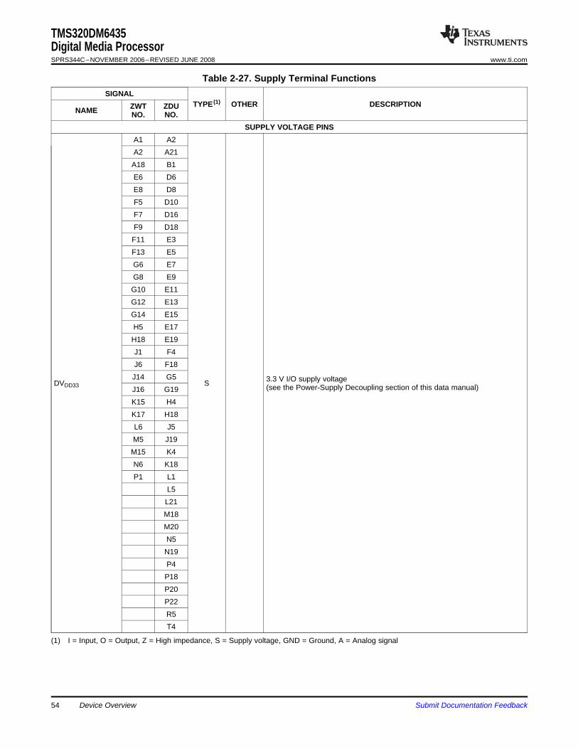
TMS320DM6435Digital Media ProcessorSPRS344C–NOVEMBER 2006–REVISED JUNE 2008 www.ti.com
Table 2-27. Supply Terminal FunctionsSIGNAL
TYPE (1) OTHER DESCRIPTIONZWT ZDUNAME NO. NO.SUPPLY VOLTAGE PINS
A1 A2A2 A21A18 B1E6 D6E8 D8F5 D10F7 D16F9 D18F11 E3F13 E5G6 E7G8 E9G10 E11G12 E13G14 E15H5 E17H18 E19J1 F4J6 F18J14 G5 3.3 V I/O supply voltageDVDD33 S (see the Power-Supply Decoupling section of this data manual)J16 G19K15 H4K17 H18L6 J5M5 J19
M15 K4N6 K18P1 L1
L5L21M18M20N5N19P4P18P20P22R5T4
(1) I = Input, O = Output, Z = High impedance, S = Supply voltage, GND = Ground, A = Analog signal
Device Overview54 Submit Documentation Feedback
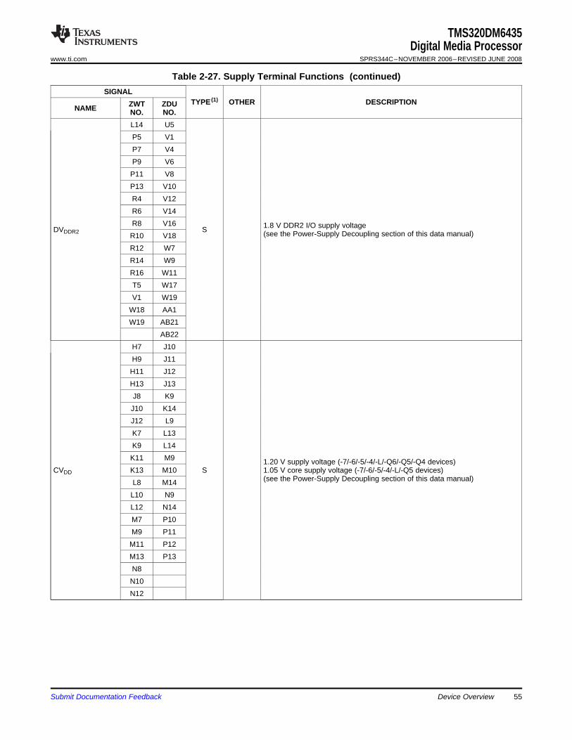
TMS320DM6435Digital Media Processor
www.ti.com SPRS344C–NOVEMBER 2006–REVISED JUNE 2008
Table 2-27. Supply Terminal Functions (continued)SIGNAL
TYPE (1) OTHER DESCRIPTIONZWT ZDUNAME NO. NO.L14 U5P5 V1P7 V4P9 V6P11 V8P13 V10R4 V12R6 V14R8 V16 1.8 V DDR2 I/O supply voltageDVDDR2 S (see the Power-Supply Decoupling section of this data manual)R10 V18R12 W7R14 W9R16 W11T5 W17V1 W19
W18 AA1W19 AB21
AB22H7 J10H9 J11H11 J12H13 J13J8 K9J10 K14J12 L9K7 L13K9 L14K11 M9 1.20 V supply voltage (-7/-6/-5/-4/-L/-Q6/-Q5/-Q4 devices)
CVDD K13 M10 S 1.05 V core supply voltage (-7/-6/-5/-4/-L/-Q5 devices)(see the Power-Supply Decoupling section of this data manual)L8 M14
L10 N9L12 N14M7 P10M9 P11
M11 P12M13 P13N8N10N12
Submit Documentation Feedback Device Overview 55
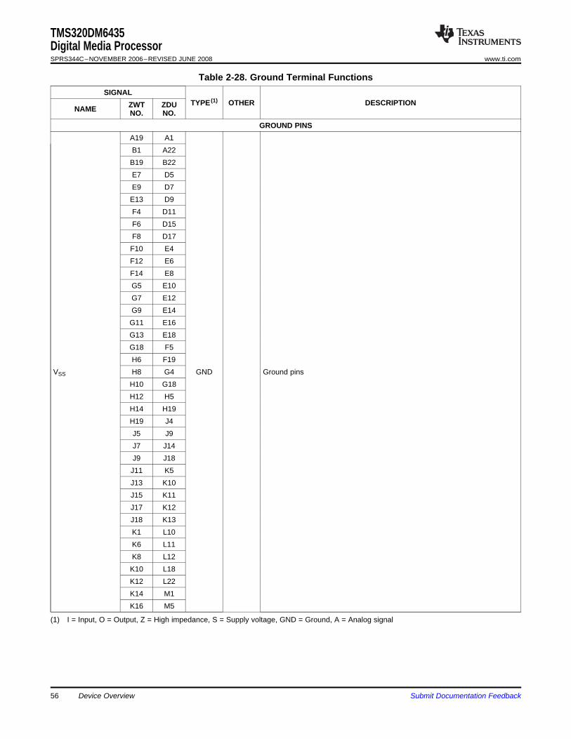
TMS320DM6435Digital Media ProcessorSPRS344C–NOVEMBER 2006–REVISED JUNE 2008 www.ti.com
Table 2-28. Ground Terminal FunctionsSIGNAL
TYPE (1) OTHER DESCRIPTIONZWT ZDUNAME NO. NO.GROUND PINS
A19 A1B1 A22B19 B22E7 D5E9 D7E13 D9F4 D11F6 D15F8 D17F10 E4F12 E6F14 E8G5 E10G7 E12G9 E14G11 E16G13 E18G18 F5H6 F19
VSS H8 G4 GND Ground pinsH10 G18H12 H5H14 H19H19 J4J5 J9J7 J14J9 J18J11 K5J13 K10J15 K11J17 K12J18 K13K1 L10K6 L11K8 L12K10 L18K12 L22K14 M1K16 M5
(1) I = Input, O = Output, Z = High impedance, S = Supply voltage, GND = Ground, A = Analog signal
56 Device Overview Submit Documentation Feedback
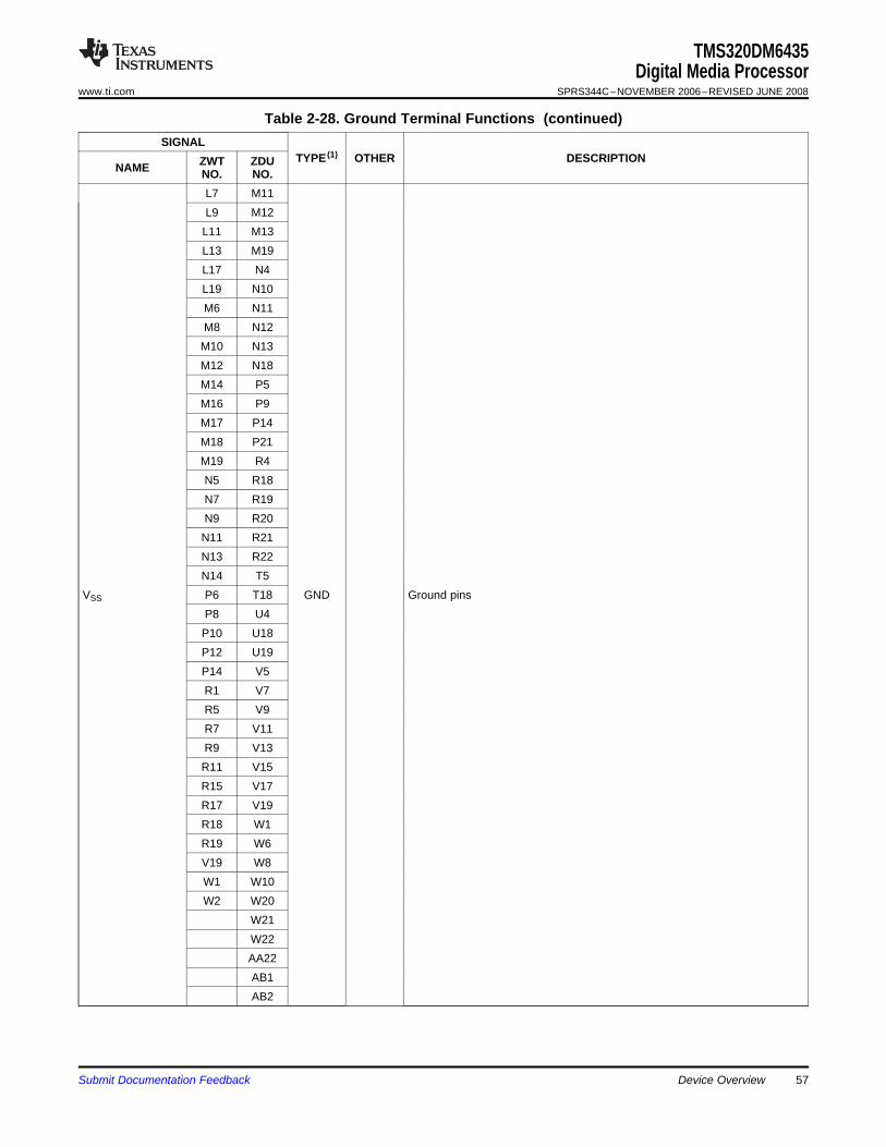
TMS320DM6435Digital Media Processor
www.ti.com SPRS344C–NOVEMBER 2006–REVISED JUNE 2008
Table 2-28. Ground Terminal Functions (continued)SIGNAL
TYPE (1) OTHER DESCRIPTIONZWT ZDUNAME NO. NO.L7 M11L9 M12
L11 M13L13 M19L17 N4L19 N10M6 N11M8 N12
M10 N13M12 N18M14 P5M16 P9M17 P14M18 P21M19 R4N5 R18N7 R19N9 R20N11 R21N13 R22N14 T5
VSS P6 T18 GND Ground pinsP8 U4P10 U18P12 U19P14 V5R1 V7R5 V9R7 V11R9 V13R11 V15R15 V17R17 V19R18 W1R19 W6V19 W8W1 W10W2 W20
W21W22AA22AB1AB2
Submit Documentation Feedback Device Overview 57
2.7 Device Support
2.7.1 Development Support
2.8 Device and Development-Support Tool Nomenclature
TMS320DM6435Digital Media ProcessorSPRS344C–NOVEMBER 2006–REVISED JUNE 2008 www.ti.com
TI offers an extensive line of development tools for the TMS320DM643x DMP platform, including tools toevaluate the performance of the processors, generate code, develop algorithm implementations, and fullyintegrate and debug software and hardware modules. The tool's support documentation is electronicallyavailable within the Code Composer Studio™ Integrated Development Environment (IDE).
The following products support development of TMS320DM643x DMP-based applications:
Software Development Tools:Code Composer Studio™ Integrated Development Environment (IDE): including EditorC/C++/Assembly Code Generation, and Debug plus additional development toolsScalable, Real-Time Foundation Software (DSP/BIOS™), which provides the basic run-time targetsoftware needed to support any SoC application.
Hardware Development Tools:Extended Development System (XDS™) Emulator (supports TMS320DM643x DMP multiprocessorsystem debug) EVM (Evaluation Module)For a complete listing of development-support tools for the TMS320DM643x DMP platform, visit theTexas Instruments web site on the Worldwide Web at http://www.ti.com uniform resource locator(URL). For information on pricing and availability, contact the nearest TI field sales office or authorizeddistributor.
To designate the stages in the product development cycle, TI assigns prefixes to the part numbers of allDSP devices and support tools. Each DSP commercial family member has one of three prefixes: TMX,TMP, or TMS (e.g., TMX320DM6435ZWT400). Texas Instruments recommends two of three possibleprefix designators for its support tools: TMDX and TMDS. These prefixes represent evolutionary stages ofproduct development from engineering prototypes (TMX/TMDX) through fully qualified productiondevices/tools (TMS/TMDS).
Device development evolutionary flow:
TMX Experimental device that is not necessarily representative of the final device's electricalspecifications.
TMP Final silicon die that conforms to the device's electrical specifications but has not completedquality and reliability verification.
TMS Fully-qualified production device.
Support tool development evolutionary flow:
TMDX Development-support product that has not yet completed Texas Instruments internalqualification testing.
TMDS Fully qualified development-support product.
TMX and TMP devices and TMDX development-support tools are shipped against the followingdisclaimer:
"Developmental product is intended for internal evaluation purposes."
TMS devices and TMDS development-support tools have been characterized fully, and the quality andreliability of the device have been demonstrated fully. TI's standard warranty applies.
Device Overview58 Submit Documentation Feedback
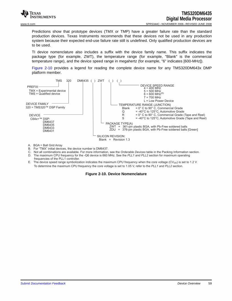
C64x+™ DSP:DM6437DM6435DM6433DM6431
PREFIX
TMS 320 DM6435 ZWT
TMX = Experimental deviceTMS = Qualified device
DEVICE FAMILY320 = TMS320™ DSP Family
PACKAGE TYPE(A)ZWT = 361-pin plastic BGA, with Pb-Free soldered ballsZDU = 376-pin plastic BGA, with Pb-Free soldered balls [Green]
DEVICE
A. BGA = Ball Grid ArrayB. For “TMX” initial devices, the device number is DM6437.C. Not all combinations are available. For more information, see the table in the Packing Information section.D. The maximum CPU frequency for the -Q6 device is 660 MHz. See the section for maximum operating
frequencies of the PLL1 controller.E
Orderable Devices
PLL1 and PLL2
. The device speed range symbolization indicates the maximum CPU frequency when the core voltage (CVDD) is set to 1.2 V.
To determine the maximum CPU frequency the core voltage is set to 1.05 V, refer to the section.PLL1 and PLL2
DEVICE SPEED RANGE
( )
4 = 400 MHz5 = 500 MHz6 = 600 MHz7 = 700 MHzL = Low Power Device
(D)
TEMPERATURE RANGE (JUNCTION)
( )( )
SILICON REVISION:Blank = Revision 1.3
Blank = 0° C to 90° C, Commercial GradeQ = -40°C to 125°C, Automotive GradeR = 0° C to 90° C, Commercial Grade (Tape and Reel)S = -40°C to 125°C, Automotive Grade (Tape and Reel)
TMS320DM6435Digital Media Processor
www.ti.com SPRS344C–NOVEMBER 2006–REVISED JUNE 2008
Predictions show that prototype devices (TMX or TMP) have a greater failure rate than the standardproduction devices. Texas Instruments recommends that these devices not be used in any productionsystem because their expected end-use failure rate still is undefined. Only qualified production devices areto be used.
TI device nomenclature also includes a suffix with the device family name. This suffix indicates thepackage type (for example, ZWT), the temperature range (for example, "Blank" is the commercialtemperature range), and the device speed range in megahertz (for example, "6" indicates [600-MHz]).
Figure 2-10 provides a legend for reading the complete device name for any TMS320DM643x DMPplatform member.
Figure 2-10. Device Nomenclature
Submit Documentation Feedback Device Overview 59
2.9 Documentation Support
2.9.1 Related Documentation From Texas Instruments
TMS320DM6435Digital Media ProcessorSPRS344C–NOVEMBER 2006–REVISED JUNE 2008 www.ti.com
The following documents describe the TMS320DM643x Digital Media Processor (DMP). Copies of thesedocuments are available on the Internet at www.ti.com. Tip: Enter the literature number in the search boxprovided at www.ti.com.
The current documentation that describes the DM643x DMP, related peripherals, and other technicalcollateral, is available in the C6000 DSP product folder at: www.ti.com/c6000.
SPRU978 TMS320DM643x DMP DSP Subsystem Reference Guide. Describes the digital signalprocessor (DSP) subsystem in the TMS320DM643x Digital Media Processor (DMP).
SPRU983 TMS320DM643x DMP Peripherals Overview Reference Guide. Provides an overview andbriefly describes the peripherals available on the TMS320DM643x Digital Media Processor(DMP).
SPRAA84 TMS320C64x to TMS320C64x+ CPU Migration Guide. Describes migrating from the TexasInstruments TMS320C64x digital signal processor (DSP) to the TMS320C64x+ DSP. Theobjective of this document is to indicate differences between the two cores. Functionality inthe devices that is identical is not included.
SPRU732 TMS320C64x/C64x+ DSP CPU and Instruction Set Reference Guide. Describes the CPUarchitecture, pipeline, instruction set, and interrupts for the TMS320C64x and TMS320C64x+digital signal processors (DSPs) of the TMS320C6000 DSP family. The C64x/C64x+ DSPgeneration comprises fixed-point devices in the C6000 DSP platform. The C64x+ DSP is anenhancement of the C64x DSP with added functionality and an expanded instruction set.
SPRU871 TMS320C64x+ DSP Megamodule Reference Guide. Describes the TMS320C64x+ digitalsignal processor (DSP) megamodule. Included is a discussion on the internal direct memoryaccess (IDMA) controller, the interrupt controller, the power-down controller, memoryprotection, bandwidth management, and the memory and cache.
Device Overview60 Submit Documentation Feedback
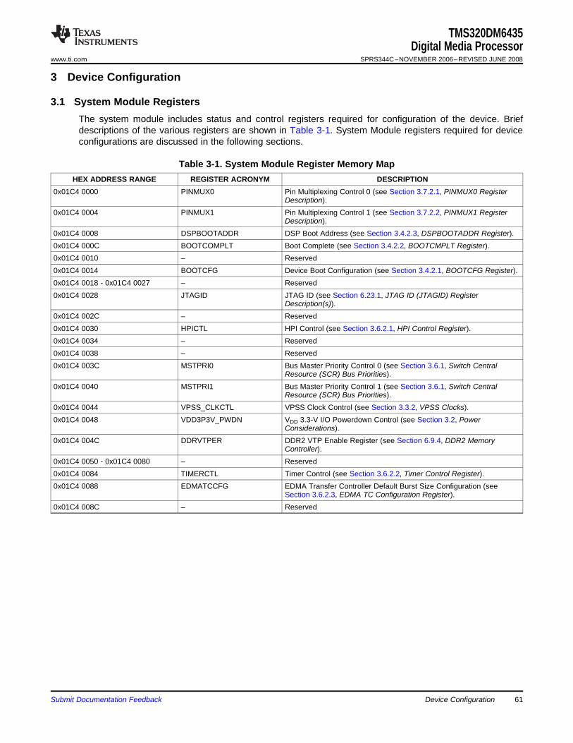
3 Device Configuration
3.1 System Module Registers
TMS320DM6435Digital Media Processor
www.ti.com SPRS344C–NOVEMBER 2006–REVISED JUNE 2008
The system module includes status and control registers required for configuration of the device. Briefdescriptions of the various registers are shown in Table 3-1. System Module registers required for deviceconfigurations are discussed in the following sections.
Table 3-1. System Module Register Memory MapHEX ADDRESS RANGE REGISTER ACRONYM DESCRIPTION
0x01C4 0000 PINMUX0 Pin Multiplexing Control 0 (see Section 3.7.2.1, PINMUX0 RegisterDescription).
0x01C4 0004 PINMUX1 Pin Multiplexing Control 1 (see Section 3.7.2.2, PINMUX1 RegisterDescription).
0x01C4 0008 DSPBOOTADDR DSP Boot Address (see Section 3.4.2.3, DSPBOOTADDR Register).0x01C4 000C BOOTCOMPLT Boot Complete (see Section 3.4.2.2, BOOTCMPLT Register).0x01C4 0010 – Reserved0x01C4 0014 BOOTCFG Device Boot Configuration (see Section 3.4.2.1, BOOTCFG Register).0x01C4 0018 - 0x01C4 0027 – Reserved0x01C4 0028 JTAGID JTAG ID (see Section 6.23.1, JTAG ID (JTAGID) Register
Description(s)).0x01C4 002C – Reserved0x01C4 0030 HPICTL HPI Control (see Section 3.6.2.1, HPI Control Register).0x01C4 0034 – Reserved0x01C4 0038 – Reserved0x01C4 003C MSTPRI0 Bus Master Priority Control 0 (see Section 3.6.1, Switch Central
Resource (SCR) Bus Priorities).0x01C4 0040 MSTPRI1 Bus Master Priority Control 1 (see Section 3.6.1, Switch Central
Resource (SCR) Bus Priorities).0x01C4 0044 VPSS_CLKCTL VPSS Clock Control (see Section 3.3.2, VPSS Clocks).0x01C4 0048 VDD3P3V_PWDN VDD 3.3-V I/O Powerdown Control (see Section 3.2, Power
Considerations).0x01C4 004C DDRVTPER DDR2 VTP Enable Register (see Section 6.9.4, DDR2 Memory
Controller).0x01C4 0050 - 0x01C4 0080 – Reserved0x01C4 0084 TIMERCTL Timer Control (see Section 3.6.2.2, Timer Control Register).0x01C4 0088 EDMATCCFG EDMA Transfer Controller Default Burst Size Configuration (see
Section 3.6.2.3, EDMA TC Configuration Register).0x01C4 008C – Reserved
Submit Documentation Feedback Device Configuration 61
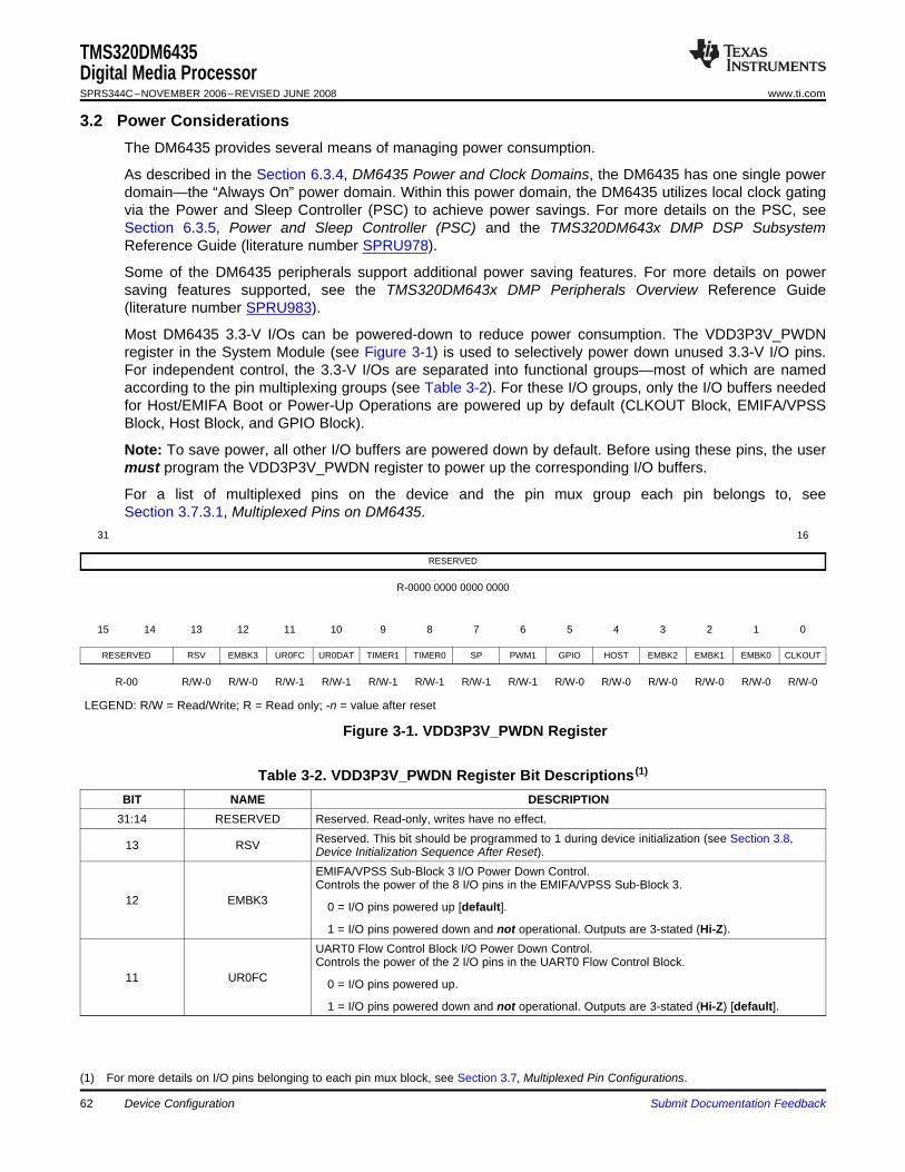
3.2 Power Considerations
TMS320DM6435Digital Media ProcessorSPRS344C–NOVEMBER 2006–REVISED JUNE 2008 www.ti.com
The DM6435 provides several means of managing power consumption.
As described in the Section 6.3.4, DM6435 Power and Clock Domains, the DM6435 has one single powerdomain—the “Always On” power domain. Within this power domain, the DM6435 utilizes local clock gatingvia the Power and Sleep Controller (PSC) to achieve power savings. For more details on the PSC, seeSection 6.3.5, Power and Sleep Controller (PSC) and the TMS320DM643x DMP DSP SubsystemReference Guide (literature number SPRU978).
Some of the DM6435 peripherals support additional power saving features. For more details on powersaving features supported, see the TMS320DM643x DMP Peripherals Overview Reference Guide(literature number SPRU983).
Most DM6435 3.3-V I/Os can be powered-down to reduce power consumption. The VDD3P3V_PWDNregister in the System Module (see Figure 3-1) is used to selectively power down unused 3.3-V I/O pins.For independent control, the 3.3-V I/Os are separated into functional groups—most of which are namedaccording to the pin multiplexing groups (see Table 3-2). For these I/O groups, only the I/O buffers neededfor Host/EMIFA Boot or Power-Up Operations are powered up by default (CLKOUT Block, EMIFA/VPSSBlock, Host Block, and GPIO Block).
Note: To save power, all other I/O buffers are powered down by default. Before using these pins, the usermust program the VDD3P3V_PWDN register to power up the corresponding I/O buffers.
For a list of multiplexed pins on the device and the pin mux group each pin belongs to, seeSection 3.7.3.1, Multiplexed Pins on DM6435.
31 16
RESERVED
R-0000 0000 0000 0000
15 14 13 12 11 10 9 8 7 6 5 4 3 2 1 0
RESERVED RSV EMBK3 UR0FC UR0DAT TIMER1 TIMER0 SP PWM1 GPIO HOST EMBK2 EMBK1 EMBK0 CLKOUT
R-00 R/W-0 R/W-0 R/W-1 R/W-1 R/W-1 R/W-1 R/W-1 R/W-1 R/W-0 R/W-0 R/W-0 R/W-0 R/W-0 R/W-0
LEGEND: R/W = Read/Write; R = Read only; -n = value after reset
Figure 3-1. VDD3P3V_PWDN Register
Table 3-2. VDD3P3V_PWDN Register Bit Descriptions (1)
BIT NAME DESCRIPTION31:14 RESERVED Reserved. Read-only, writes have no effect.
Reserved. This bit should be programmed to 1 during device initialization (see Section 3.8,13 RSV Device Initialization Sequence After Reset).EMIFA/VPSS Sub-Block 3 I/O Power Down Control.Controls the power of the 8 I/O pins in the EMIFA/VPSS Sub-Block 3.
12 EMBK3 0 = I/O pins powered up [default].
1 = I/O pins powered down and not operational. Outputs are 3-stated (Hi-Z).UART0 Flow Control Block I/O Power Down Control.Controls the power of the 2 I/O pins in the UART0 Flow Control Block.
11 UR0FC 0 = I/O pins powered up.
1 = I/O pins powered down and not operational. Outputs are 3-stated (Hi-Z) [default].
(1) For more details on I/O pins belonging to each pin mux block, see Section 3.7, Multiplexed Pin Configurations.
Device Configuration62 Submit Documentation Feedback
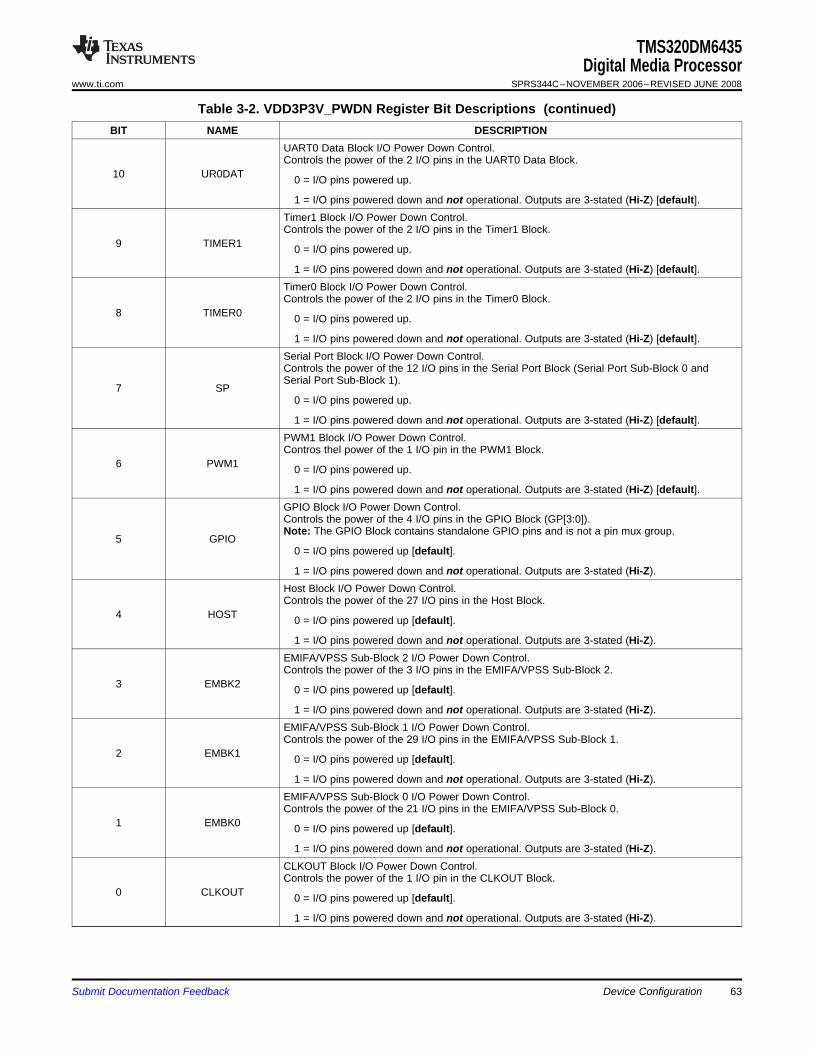
TMS320DM6435Digital Media Processor
www.ti.com SPRS344C–NOVEMBER 2006–REVISED JUNE 2008
Table 3-2. VDD3P3V_PWDN Register Bit Descriptions (continued)BIT NAME DESCRIPTION
UART0 Data Block I/O Power Down Control.Controls the power of the 2 I/O pins in the UART0 Data Block.
10 UR0DAT 0 = I/O pins powered up.
1 = I/O pins powered down and not operational. Outputs are 3-stated (Hi-Z) [default].Timer1 Block I/O Power Down Control.Controls the power of the 2 I/O pins in the Timer1 Block.
9 TIMER1 0 = I/O pins powered up.
1 = I/O pins powered down and not operational. Outputs are 3-stated (Hi-Z) [default].Timer0 Block I/O Power Down Control.Controls the power of the 2 I/O pins in the Timer0 Block.
8 TIMER0 0 = I/O pins powered up.
1 = I/O pins powered down and not operational. Outputs are 3-stated (Hi-Z) [default].Serial Port Block I/O Power Down Control.Controls the power of the 12 I/O pins in the Serial Port Block (Serial Port Sub-Block 0 andSerial Port Sub-Block 1).
7 SP0 = I/O pins powered up.
1 = I/O pins powered down and not operational. Outputs are 3-stated (Hi-Z) [default].PWM1 Block I/O Power Down Control.Contros thel power of the 1 I/O pin in the PWM1 Block.
6 PWM1 0 = I/O pins powered up.
1 = I/O pins powered down and not operational. Outputs are 3-stated (Hi-Z) [default].GPIO Block I/O Power Down Control.Controls the power of the 4 I/O pins in the GPIO Block (GP[3:0]).Note: The GPIO Block contains standalone GPIO pins and is not a pin mux group.
5 GPIO0 = I/O pins powered up [default].
1 = I/O pins powered down and not operational. Outputs are 3-stated (Hi-Z).Host Block I/O Power Down Control.Controls the power of the 27 I/O pins in the Host Block.
4 HOST 0 = I/O pins powered up [default].
1 = I/O pins powered down and not operational. Outputs are 3-stated (Hi-Z).EMIFA/VPSS Sub-Block 2 I/O Power Down Control.Controls the power of the 3 I/O pins in the EMIFA/VPSS Sub-Block 2.
3 EMBK2 0 = I/O pins powered up [default].
1 = I/O pins powered down and not operational. Outputs are 3-stated (Hi-Z).EMIFA/VPSS Sub-Block 1 I/O Power Down Control.Controls the power of the 29 I/O pins in the EMIFA/VPSS Sub-Block 1.
2 EMBK1 0 = I/O pins powered up [default].
1 = I/O pins powered down and not operational. Outputs are 3-stated (Hi-Z).EMIFA/VPSS Sub-Block 0 I/O Power Down Control.Controls the power of the 21 I/O pins in the EMIFA/VPSS Sub-Block 0.
1 EMBK0 0 = I/O pins powered up [default].
1 = I/O pins powered down and not operational. Outputs are 3-stated (Hi-Z).CLKOUT Block I/O Power Down Control.Controls the power of the 1 I/O pin in the CLKOUT Block.
0 CLKOUT 0 = I/O pins powered up [default].
1 = I/O pins powered down and not operational. Outputs are 3-stated (Hi-Z).
Submit Documentation Feedback Device Configuration 63
3.3 Clock Considerations
3.3.1 Clock Configurations after Device Reset
3.3.1.1 Device Clock Frequency
3.3.1.2 Module Clock State
TMS320DM6435Digital Media ProcessorSPRS344C–NOVEMBER 2006–REVISED JUNE 2008 www.ti.com
Global device and local peripheral clocks are controlled by the PLL Controllers (PLLC1 and PLLC2) andthe Power and Sleep Controller (PSC). In addition, the System Module VPSS_CLKCTL register configuresthe clock source to the Video Processing Subsystem (VPSS).
After device reset, the user is responsible for programming the PLL Controllers (PLLC1 and PLLC2) andthe Power and Sleep Controller (PSC) to bring the device up to the desired clock frequency and thedesired peripheral clock state (clock gating or not).
For additional power savings, some of the DM6435 peripherals support clock gating within the peripheralboundary. For more details on clock gating and power saving features supported by a specific peripheral,see the peripheral-specific reference guides [listed/linked in the TMS320DM643x DMP PeripheralsOverview Reference Guide (literature number SPRU983)].
The DM6435 defaults to PLL bypass mode. To bring the device up to the desired clock frequency, theuser should program PLLC1 and PLLC2 after device reset.
DM6435 supports a FASTBOOT option, where upon exit from device reset the internal bootloader codeautomatically programs the PLLC1 into PLL mode with a specific PLL multiplier and divider to speed updevice boot. While the FASTBOOT option is beneficial for faster boot, the PLL multiplier and dividerselected for boot may not be the exact frequency desired for the run-time application. It is the user'sresponsibility to reconfigure PLLC1 after fastboot to bring the device into the desired clock frequency.Section 3.4.1, Boot Modes discusses the different fast boot modes in more detail.
The user must adhere to the various clock requirements when programming the PLLC1 and PLLC2:• Fixed frequency ratio requirements between CLKDIV1, CLKDIV3, and CLKDIV6 clock domains. For
more details on the frequency ratio requirements, see Section 6.3.4, DM6435 Power and ClockDomains.
• PLL multiplier and frequency ranges. For more details on PLL multiplier and frequency ranges, seeSection 6.7.1, PLL1 and PLL2.
The clock and reset state for each of the modules is controlled by the Power and Sleep Controller (PSC).Table 3-3 shows the default state of each module after a device-level global reset. The DM6435 devicehas four different module states—Enable, Disable, SyncReset, or SwRstDisable. For more information onthe definitions of the module states, the PSC, and PSC programming, see Section 6.3.5, Power and SleepController (PSC) and the TMS320DM643x DMP DSP Subsystem Reference Guide (literature numberSPRU978).
Device Configuration64 Submit Documentation Feedback
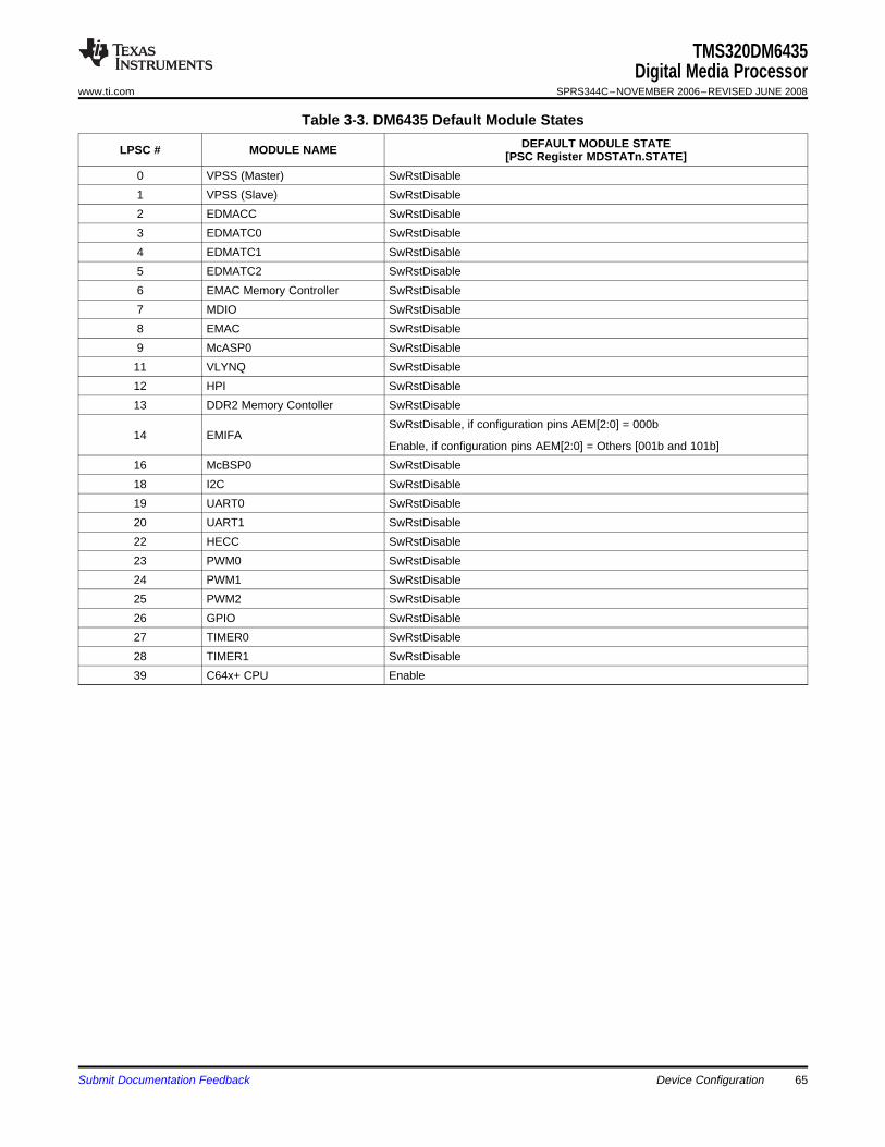
TMS320DM6435Digital Media Processor
www.ti.com SPRS344C–NOVEMBER 2006–REVISED JUNE 2008
Table 3-3. DM6435 Default Module StatesDEFAULT MODULE STATELPSC # MODULE NAME [PSC Register MDSTATn.STATE]
0 VPSS (Master) SwRstDisable1 VPSS (Slave) SwRstDisable2 EDMACC SwRstDisable3 EDMATC0 SwRstDisable4 EDMATC1 SwRstDisable5 EDMATC2 SwRstDisable6 EMAC Memory Controller SwRstDisable7 MDIO SwRstDisable8 EMAC SwRstDisable9 McASP0 SwRstDisable
11 VLYNQ SwRstDisable12 HPI SwRstDisable13 DDR2 Memory Contoller SwRstDisable
SwRstDisable, if configuration pins AEM[2:0] = 000b14 EMIFA
Enable, if configuration pins AEM[2:0] = Others [001b and 101b]16 McBSP0 SwRstDisable18 I2C SwRstDisable19 UART0 SwRstDisable20 UART1 SwRstDisable22 HECC SwRstDisable23 PWM0 SwRstDisable24 PWM1 SwRstDisable25 PWM2 SwRstDisable26 GPIO SwRstDisable27 TIMER0 SwRstDisable28 TIMER1 SwRstDisable39 C64x+ CPU Enable
Submit Documentation Feedback Device Configuration 65
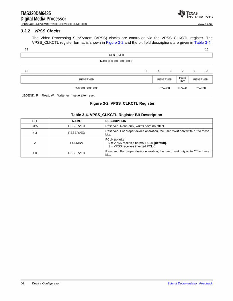
3.3.2 VPSS Clocks
TMS320DM6435Digital Media ProcessorSPRS344C–NOVEMBER 2006–REVISED JUNE 2008 www.ti.com
The Video Processing SubSystem (VPSS) clocks are controlled via the VPSS_CLKCTL register. TheVPSS_CLKCTL register format is shown in Figure 3-2 and the bit field descriptions are given in Table 3-4.
31 16
RESERVED
R-0000 0000 0000 0000
15 5 4 3 2 1 0
PCLKRESERVED RESERVED RESERVEDINV
R-0000 0000 000 R/W-00 R/W-0 R/W-00
LEGEND: R = Read; W = Write; -n = value after reset
Figure 3-2. VPSS_CLKCTL Register
Table 3-4. VPSS_CLKCTL Register Bit DescriptionBIT NAME DESCRIPTION31:5 RESERVED Reserved. Read-only, writes have no effect.
Reserved. For proper device operation, the user must only write "0" to these4:3 RESERVED bits.PCLK polarity
2 PCLKINV 0 = VPSS receives normal PCLK [default].1 = VPSS receives inverted PCLK.
Reserved. For proper device operation, the user must only write "0" to these1:0 RESERVED bits.
Device Configuration66 Submit Documentation Feedback
3.4 Boot Sequence
3.4.1 Boot Modes
TMS320DM6435Digital Media Processor
www.ti.com SPRS344C–NOVEMBER 2006–REVISED JUNE 2008
The boot sequence is a process by which the device's memory is loaded with program and data sections,and by which some of the device's internal registers are programmed with predetermined values. The bootsequence is started automatically after each device-level global reset. For more details on device-levelglobal resets, see Section 6.5, Reset.
There are several methods by which the memory and register initialization can take place. Each of thesemethods is referred to as a boot mode. The boot mode to be used is selected at reset. For moreinformation on the bootmode selections, see Section 3.4.1, Boot Modes.
The device is booted through multiple means—primary bootloaders within internal ROM or EMIFA, andsecondary user bootloaders from peripherals or external memories. Boot modes, pin configurations, andregister configurations required for booting the device, are described in the following subsections.
The DM6435 boot modes are determined by these device boot and configuration pins. For information onhow these pins are sampled at device reset, see Section 6.5.1.2, Latching Boot and Configuration Pins.• BOOTMODE[3:0]• FASTBOOT• AEM[2:0]• PLLMS[2:0]
Note: the PLLMS[2:0] configuration pins are actually multiplexed with the AEAW[2:0] configuration pins.For more details on the multiplexed AEAW[2:0]/PLLMS[2:0] configuration pins and control, seeSection 3.5.1.2, EMIFA Address Width Selects (AEAW[2:0]) and FASTBOOT PLL Multiplier Selects(PLLMS[2:0]).
BOOTMODE[3:0] determines the type of boot (e.g., I2C Boot, EMIFA Boot, or HPI Boot, etc.). FASTBOOTdetermines if the PLL is enabled during boot to speed up the boot process.
The combination of AEM[2:0] and PLLMS[2:0] is used by bootloader code to determine the PLL multiplierused during fastboot modes (FASTBOOT = 1).
The DM6435 boot modes are grouped into three categories—Non-Fastboot Modes, Fixed-MultiplierFastboot Modes, and User-Select Multiplier Fastboot Modes.
• Non-Fastboot Modes (FASTBOOT = 0): The device operates in default PLL bypass mode duringboot. The Non-Fastboot bootmodes available on the DM6435 are shown in Table 3-5.
• Fixed-Multiplier Fastboot Modes (FASTBOOT = 1, AEM[2:0] = 001b): The bootloader code speedsup the device during boot according to the fixed PLL multipliers. The Fixed-Multiplier Fastbootbootmodes available on the DM6435 are shown in Table 3-6.Note: The PLLMS[2:0] configurations have no effect on the Fixed-Multiplier Fastboot Modes, as thesepins function as AEAW[2:0] to select the EMIFA address width when AEM[2:0] = 001b.
• User-Select Multiplier Fastboot Modes (FASTBOOT = 1, AEM[2:0] = 000b and 101b): Thebootloader code speeds up the device during boot. The PLL multiplier is selected by the user via thePLLMS[2:0] pins. The User-Select Multiplier Fastboot bootmodes available on the DM6435 are shownin Table 3-7.
All other modes not shown in these tables are reserved and invalid settings.
For more information on how these pins are sampled at device reset, see Section 6.5.1.2, Latching Bootand Configuration Pins.
Submit Documentation Feedback Device Configuration 67
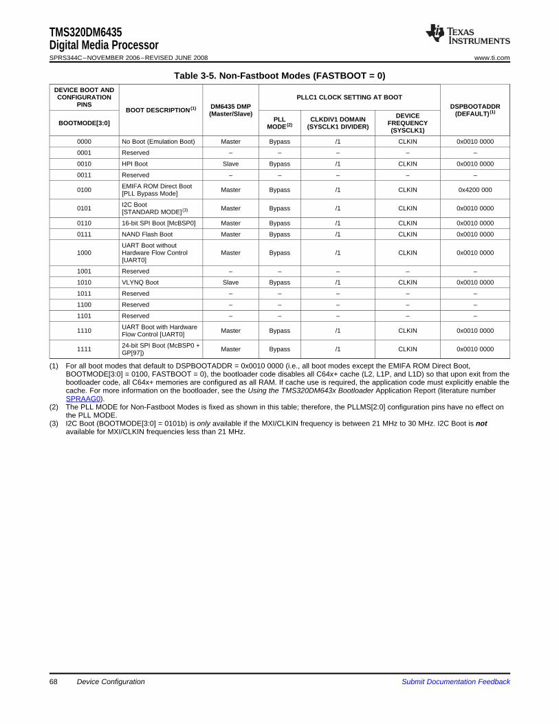
TMS320DM6435Digital Media ProcessorSPRS344C–NOVEMBER 2006–REVISED JUNE 2008 www.ti.com
Table 3-5. Non-Fastboot Modes (FASTBOOT = 0)DEVICE BOOT ANDCONFIGURATION PLLC1 CLOCK SETTING AT BOOT
PINS DM6435 DMP DSPBOOTADDRBOOT DESCRIPTION (1)(Master/Slave) (DEFAULT) (1)
DEVICEPLL CLKDIV1 DOMAINBOOTMODE[3:0] FREQUENCYMODE (2) (SYSCLK1 DIVIDER) (SYSCLK1)
0000 No Boot (Emulation Boot) Master Bypass /1 CLKIN 0x0010 0000
0001 Reserved – – – – –
0010 HPI Boot Slave Bypass /1 CLKIN 0x0010 0000
0011 Reserved – – – – –
EMIFA ROM Direct Boot0100 Master Bypass /1 CLKIN 0x4200 000[PLL Bypass Mode]
I2C Boot0101 Master Bypass /1 CLKIN 0x0010 0000[STANDARD MODE] (3)
0110 16-bit SPI Boot [McBSP0] Master Bypass /1 CLKIN 0x0010 0000
0111 NAND Flash Boot Master Bypass /1 CLKIN 0x0010 0000
UART Boot without1000 Hardware Flow Control Master Bypass /1 CLKIN 0x0010 0000
[UART0]
1001 Reserved – – – – –
1010 VLYNQ Boot Slave Bypass /1 CLKIN 0x0010 0000
1011 Reserved – – – – –
1100 Reserved – – – – –
1101 Reserved – – – – –
UART Boot with Hardware1110 Master Bypass /1 CLKIN 0x0010 0000Flow Control [UART0]
24-bit SPI Boot (McBSP0 +1111 Master Bypass /1 CLKIN 0x0010 0000GP[97])
(1) For all boot modes that default to DSPBOOTADDR = 0x0010 0000 (i.e., all boot modes except the EMIFA ROM Direct Boot,BOOTMODE[3:0] = 0100, FASTBOOT = 0), the bootloader code disables all C64x+ cache (L2, L1P, and L1D) so that upon exit from thebootloader code, all C64x+ memories are configured as all RAM. If cache use is required, the application code must explicitly enable thecache. For more information on the bootloader, see the Using the TMS320DM643x Bootloader Application Report (literature numberSPRAAG0).
(2) The PLL MODE for Non-Fastboot Modes is fixed as shown in this table; therefore, the PLLMS[2:0] configuration pins have no effect onthe PLL MODE.
(3) I2C Boot (BOOTMODE[3:0] = 0101b) is only available if the MXI/CLKIN frequency is between 21 MHz to 30 MHz. I2C Boot is notavailable for MXI/CLKIN frequencies less than 21 MHz.
68 Device Configuration Submit Documentation Feedback
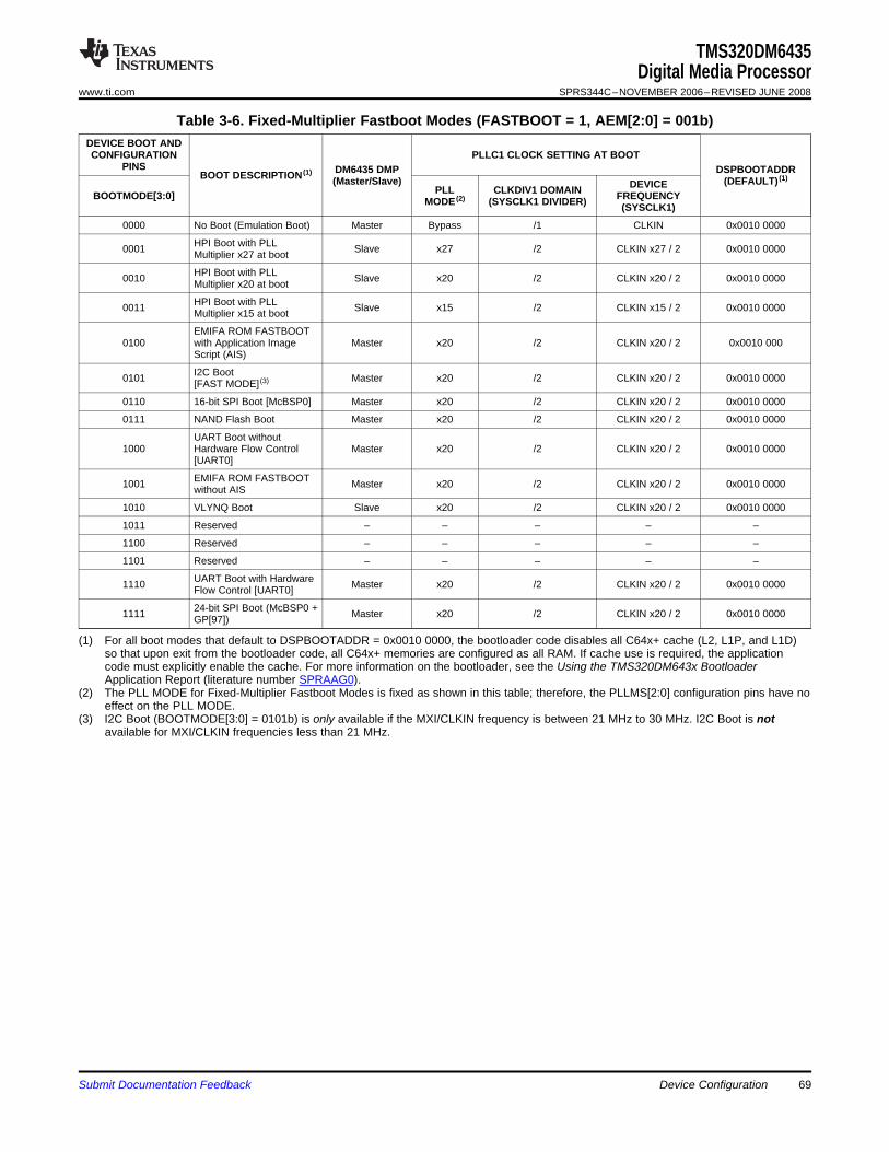
TMS320DM6435Digital Media Processor
www.ti.com SPRS344C–NOVEMBER 2006–REVISED JUNE 2008
Table 3-6. Fixed-Multiplier Fastboot Modes (FASTBOOT = 1, AEM[2:0] = 001b)DEVICE BOOT ANDCONFIGURATION PLLC1 CLOCK SETTING AT BOOT
PINS DM6435 DMP DSPBOOTADDRBOOT DESCRIPTION (1)(Master/Slave) (DEFAULT) (1)
DEVICEPLL CLKDIV1 DOMAINBOOTMODE[3:0] FREQUENCYMODE (2) (SYSCLK1 DIVIDER) (SYSCLK1)
0000 No Boot (Emulation Boot) Master Bypass /1 CLKIN 0x0010 0000
HPI Boot with PLL0001 Slave x27 /2 CLKIN x27 / 2 0x0010 0000Multiplier x27 at boot
HPI Boot with PLL0010 Slave x20 /2 CLKIN x20 / 2 0x0010 0000Multiplier x20 at boot
HPI Boot with PLL0011 Slave x15 /2 CLKIN x15 / 2 0x0010 0000Multiplier x15 at boot
EMIFA ROM FASTBOOT0100 with Application Image Master x20 /2 CLKIN x20 / 2 0x0010 000
Script (AIS)
I2C Boot0101 Master x20 /2 CLKIN x20 / 2 0x0010 0000[FAST MODE] (3)
0110 16-bit SPI Boot [McBSP0] Master x20 /2 CLKIN x20 / 2 0x0010 0000
0111 NAND Flash Boot Master x20 /2 CLKIN x20 / 2 0x0010 0000
UART Boot without1000 Hardware Flow Control Master x20 /2 CLKIN x20 / 2 0x0010 0000
[UART0]
EMIFA ROM FASTBOOT1001 Master x20 /2 CLKIN x20 / 2 0x0010 0000without AIS
1010 VLYNQ Boot Slave x20 /2 CLKIN x20 / 2 0x0010 0000
1011 Reserved – – – – –
1100 Reserved – – – – –
1101 Reserved – – – – –
UART Boot with Hardware1110 Master x20 /2 CLKIN x20 / 2 0x0010 0000Flow Control [UART0]
24-bit SPI Boot (McBSP0 +1111 Master x20 /2 CLKIN x20 / 2 0x0010 0000GP[97])
(1) For all boot modes that default to DSPBOOTADDR = 0x0010 0000, the bootloader code disables all C64x+ cache (L2, L1P, and L1D)so that upon exit from the bootloader code, all C64x+ memories are configured as all RAM. If cache use is required, the applicationcode must explicitly enable the cache. For more information on the bootloader, see the Using the TMS320DM643x BootloaderApplication Report (literature number SPRAAG0).
(2) The PLL MODE for Fixed-Multiplier Fastboot Modes is fixed as shown in this table; therefore, the PLLMS[2:0] configuration pins have noeffect on the PLL MODE.
(3) I2C Boot (BOOTMODE[3:0] = 0101b) is only available if the MXI/CLKIN frequency is between 21 MHz to 30 MHz. I2C Boot is notavailable for MXI/CLKIN frequencies less than 21 MHz.
Submit Documentation Feedback Device Configuration 69
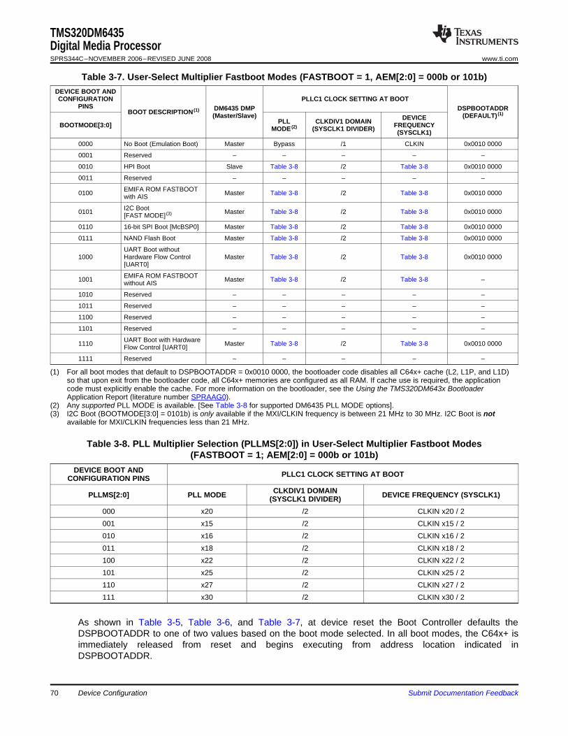
TMS320DM6435Digital Media ProcessorSPRS344C–NOVEMBER 2006–REVISED JUNE 2008 www.ti.com
Table 3-7. User-Select Multiplier Fastboot Modes (FASTBOOT = 1, AEM[2:0] = 000b or 101b)DEVICE BOOT ANDCONFIGURATION PLLC1 CLOCK SETTING AT BOOT
PINS DM6435 DMP DSPBOOTADDRBOOT DESCRIPTION (1)(Master/Slave) (DEFAULT) (1)
DEVICEPLL CLKDIV1 DOMAINBOOTMODE[3:0] FREQUENCYMODE (2) (SYSCLK1 DIVIDER) (SYSCLK1)
0000 No Boot (Emulation Boot) Master Bypass /1 CLKIN 0x0010 0000
0001 Reserved – – – – –
0010 HPI Boot Slave Table 3-8 /2 Table 3-8 0x0010 0000
0011 Reserved – – – – –
EMIFA ROM FASTBOOT0100 Master Table 3-8 /2 Table 3-8 0x0010 0000with AIS
I2C Boot0101 Master Table 3-8 /2 Table 3-8 0x0010 0000[FAST MODE] (3)
0110 16-bit SPI Boot [McBSP0] Master Table 3-8 /2 Table 3-8 0x0010 0000
0111 NAND Flash Boot Master Table 3-8 /2 Table 3-8 0x0010 0000
UART Boot without1000 Hardware Flow Control Master Table 3-8 /2 Table 3-8 0x0010 0000
[UART0]
EMIFA ROM FASTBOOT1001 Master Table 3-8 /2 Table 3-8 –without AIS
1010 Reserved – – – – –
1011 Reserved – – – – –
1100 Reserved – – – – –
1101 Reserved – – – – –
UART Boot with Hardware1110 Master Table 3-8 /2 Table 3-8 0x0010 0000Flow Control [UART0]
1111 Reserved – – – – –
(1) For all boot modes that default to DSPBOOTADDR = 0x0010 0000, the bootloader code disables all C64x+ cache (L2, L1P, and L1D)so that upon exit from the bootloader code, all C64x+ memories are configured as all RAM. If cache use is required, the applicationcode must explicitly enable the cache. For more information on the bootloader, see the Using the TMS320DM643x BootloaderApplication Report (literature number SPRAAG0).
(2) Any supported PLL MODE is available. [See Table 3-8 for supported DM6435 PLL MODE options].(3) I2C Boot (BOOTMODE[3:0] = 0101b) is only available if the MXI/CLKIN frequency is between 21 MHz to 30 MHz. I2C Boot is not
available for MXI/CLKIN frequencies less than 21 MHz.
Table 3-8. PLL Multiplier Selection (PLLMS[2:0]) in User-Select Multiplier Fastboot Modes(FASTBOOT = 1; AEM[2:0] = 000b or 101b)
DEVICE BOOT AND PLLC1 CLOCK SETTING AT BOOTCONFIGURATION PINSCLKDIV1 DOMAINPLLMS[2:0] PLL MODE DEVICE FREQUENCY (SYSCLK1)(SYSCLK1 DIVIDER)
000 x20 /2 CLKIN x20 / 2001 x15 /2 CLKIN x15 / 2010 x16 /2 CLKIN x16 / 2011 x18 /2 CLKIN x18 / 2100 x22 /2 CLKIN x22 / 2101 x25 /2 CLKIN x25 / 2110 x27 /2 CLKIN x27 / 2111 x30 /2 CLKIN x30 / 2
As shown in Table 3-5, Table 3-6, and Table 3-7, at device reset the Boot Controller defaults theDSPBOOTADDR to one of two values based on the boot mode selected. In all boot modes, the C64x+ isimmediately released from reset and begins executing from address location indicated inDSPBOOTADDR.
Device Configuration70 Submit Documentation Feedback
3.4.1.1 FASTBOOT
TMS320DM6435Digital Media Processor
www.ti.com SPRS344C–NOVEMBER 2006–REVISED JUNE 2008
• Internal Bootloader ROM (0x0010 0000): For most boot modes, the DSPBOOTADDR defaults to theinternal Bootloader ROM so that the DSP can immediately execute the bootloader code in the internalROM. The bootloader code decodes the captured BOOTMODE, FASTBOOT, default AEM (DAEM),and PLLMS information (in the BOOTCFG register) to determine the proper boot operation.Note: For all boot modes that default to DSPBOOTADDR = 0x0010 0000, the bootloader codedisables all C64x+ cache (L2, L1P, and L1D) so that upon exit from the bootloader code, all C64x+memories are configured as all RAM. If cache use is required, the application code must explicitlyenable the cache. For more information on boot modes, see Section 3.4.1, Boot Modes. For moreinformation on the bootloader, see the Using the TMS320DM643x Bootloader Application Report(literature number SPRAAG0).
• EMIFA Chip Select Space 2 (0x4200 0000): The EMIFA ROM Direct Boot in PLL Bypass Mode(BOOTCFG settings BOOTMODE[3:0] = 0100b, FASTBOOT = 0) is the only exception where theDSPBOOTADDR defaults to the EMIFA Chip Select Space 2. The DSP begins execution directly fromthe external ROM at this EMIFA space.
For more information how the bootloader code handles each boot mode, see Using the TMS320DM643xBootloader Application Report (literature number SPRAAG0).
When DM6435 exits pin reset (RESET or POR released), the PLL Controllers (PLLC1 and PLLC2) defaultto PLL Bypass Mode. This means the PLLs are disabled, and the MXI/CLKIN clock input is driving thechip. All the clock domain divider ratios discussed in Section 6.3.4, DM6435 Power and Clock Domains,still apply. For example, assume an MXI/CLKIN frequency of 27 MHz—meaning the internal clock sourcefor EMIFA is at CLKDIV3 domain = 27 MHz/3 = 9 MHz, a very slow clock. In addition, the EMIFA registersare reset to the slowest configuration which translates to very slow peripheral operation/boot.
To optimize boot time, the user should reprogram clock settings via the PLLC as early as possible duringthe boot process. The FASTBOOT pin facilitates this operation by allowing the device to boot at a fasterclock rate.
Except for the EMIFA ROM Direct Boot in PLL Bypass Mode (BOOTCFG settings BOOTMODE[3:0] =0100b, FASTBOOT = 0), all other boot modes default to executing from the Internal Bootloader ROM. Thefirst action that the bootloader code takes is to decode the boot mode. If the FASTBOOT option isselected (BOOTCFG.FASTBOOT = 1), the bootloader software begins by programming the PLLC1(System PLLC) to PLL Mode to give the device a slightly faster operation before fetching code fromexternal devices. The exact PLL multiplier that the bootloader uses is determined by the AEM[2:0] andPLLMS[2:0] settings, as shown in Table 3-6 and Table 3-7.
Some boot modes must be accompanied with FASTBOOT = 1 so that the corresponding peripheral canrun at a reasonable rate to communicate to the external device(s).
Note: PLLC2 still stays in PLL Bypass Mode, the bootloader does not reconfigure it.
Submit Documentation Feedback Device Configuration 71
3.4.1.2 Selecting FASTBOOT PLL Multiplier
3.4.1.3 EMIFA Boot Modes
TMS320DM6435Digital Media ProcessorSPRS344C–NOVEMBER 2006–REVISED JUNE 2008 www.ti.com
Table 3-6, Table 3-7, and Table 3-8 show the PLL multipliers used by the bootloader code during fastboot(FASTBOOT = 1) and the resulting device frequency. The user is responsible for selecting the bootmodewith the appropriate PLL multiplier for their MXI/CLKIN clock source so that the device speed and PLLfrequency range requirements are met. For the PLLC1 Clock Frequency Ranges, see Table 6-15, PLLC1Clock Frequency Ranges in Section 6.7.1, PLL1 and PLL2.
The following are guidelines for PLL output frequency and device speed (frequency):• PLL Output Frequency: (PLLOUT = CLKIN frequency * boot PLL Multiplier) must stay within the
PLLOUT frequency range in Table 6-15, PLLC1 Clock Frequency Ranges.• Device Frequency: (SYSCLK1) calculated from Table 3-6 and Table 3-7 must not exceed the
SYSCLK1 maximum frequency in Table 6-15, PLLC1 Clock Frequency Ranges.For example, for a 600-MHz device with a CLKIN = 27 MHz, in order to stay within the PLLOUTfrequency range and SYSCLK1 maximum frequency from Table 6-15, PLLC1 Clock FrequencyRanges, the user must select a boot mode with a PLL1 multiplier between x15 and x22.
As shown in Table 3-5, Table 3-6, and Table 3-7, there are different types of EMIFA Boot Modes. Thissubsection summarizes these types of EMIFA boot modes. For further detailed information, see the Usingthe TMS320DM643x Bootloader Application Report (literature number SPRAAG0).• EMIFA ROM Direct Boot in PLL Bypass Mode (FASTBOOT = 0, BOOTMODE[3:0] = 0100b)
– The C64x+ fetches the code directly from EMIFA Chip Select 2 Space [EM_CS2] (address0x42000000)
– The PLL is in Bypass Mode– EMIFA is configured as Asynchronous EMIF. The user is responsible for ensuring the desirable
Asynchronous EMIF pins are available through configuration pins AEM[2:0] and AEAW[2:0].AEM[2:0] must be configured to 001b [8-bit EMIFA (Async) Pinout Mode 1].
• EMIFA ROM Fastboot with AIS (FASTBOOT = 1, BOOTMODE[3:0] = 0100b)– The C64x+ begins execution from the internal bootloader ROM at address 0x00100000.– The bootloader code programs PLLC1 to PLL Mode to speed up the boot process. The PLL
multiplier value is determined by the AEM[2:0] and PLLMS[2:0] configurations as shown inTable 3-6 and Table 3-7.
– The bootloader code reads code from the EMIFA EM_CS2 space using the application image script(AIS) format.
– EMIFA is configured as Asynchronous EMIF. The user is responsible for ensuring the desirableAsynchronous EMIF pins are available through configuration pins AEM[2:0] and AEAW[2:0].AEM[2:0] must be configured to 001b [8-bit EMIFA (Async) Pinout Mode 1].
• EMIFA ROM Fastboot without AIS: (FASTBOOT = 1, BOOTMODE[3:0] = 1001b)– The C64x+ begins execution from the internal bootloader ROM at address 0x00100000.– The bootloader code programs PLLC1 to PLL Mode to speed up the boot process. The PLL
multiplier value is determined by the AEM[2:0] and PLLMS[2:0] configurations as shown inTable 3-6 and Table 3-7.
– The bootloader code then jumps to the EMIFA EM_CS2 space, at which point the C64x+ fetchesthe code directly from address 0x42000000.
– EMIFA is configured as Asynchronous EMIF. The user is responsible for ensuring the desirableAsynchronous EMIF pins are available through configuration pins AEM[2:0] and AEAW[2:0].AEM[2:0] must be configured to 001b [8-bit EMIFA (Async) Pinout Mode 1].
Device Configuration72 Submit Documentation Feedback
3.4.1.4 Serial Boot Modes (I2C, UART[UART0], SPI[McBSP0])
TMS320DM6435Digital Media Processor
www.ti.com SPRS344C–NOVEMBER 2006–REVISED JUNE 2008
• NAND Flash Boot: (FASTBOOT = 0 or 1, BOOTMODE[3:0] = 0111b)– The C64x+ begins execution from the internal bootloader ROM at address 0x00100000.– Depending on the FASTBOOT, AEM[2:0], and PLLMS[2:0] settings, the bootloader code may
program the PLLC1 to PLL Mode to speed up the boot process. See Table 3-5, Table 3-6, andTable 3-7.
– The bootloader code reads the code from EMIFA (NAND) EM_CS2 (address 0x42000000) usingAIS format.
– EMIFA is configured in NAND mode. The user is responsible for ensuring the desirableAsynchronous EMIF pins are available through configuration pins AEM[2:0] and AEAW[2:0].AEM[2:0] can be configured to 001b [8-bit EMIFA (Async) Pinout Mode 1] or 101b [8-bit EMIFA(NAND) Pinout Mode 5].
This subsection discusses how the bootloader configures the clock dividers for the serial boot modes—I2Cboot, UART boot, and SPI boot.3.4.1.4.1 I2C Boot
If FASTBOOT = 0, then I2C Boot (BOOTMODE = 0101) is performed in Standard-Mode (up-to 100 kbps).If FASTBOOT = 1, then I2C Boot is performed in Fast-Mode (up-to 400 kbps). The actual I2C datatransfer rate is dependent on the MXI/CLKIN frequency.
This is how the bootloader programs the I2C:• I2C Boot in Fast-Mode (BOOTMODE[3:0] = 0101b, FASTBOOT = 1)
– I2C register settings: ICPSC.IPSC = 210, ICCLKL.ICCL = 810, ICCKH.ICCH = 810
– Resulting in the following I2C prescaled module clock frequency (internal I2C clock):• (CLKIN frequency in MHz) / 3
– Resulting in the following I2C serial clock (SCL):• SCL frequency (in kHz) = (CLKIN frequency in MHz) / 78 * 1000• SCL low pulse duration (in µs) = 39 / (CLKIN frequency in MHz)• SCL high pulse duration (in µs) = 39 / (CLKIN frequency in MHz)
• I2C Boot in Standard-Mode (BOOTMODE[3:0] = 0101b, FASTBOOT = 0)– I2C register settings: ICPSC.IPSC = 210, ICCLKL.ICCL = 4510, ICCKH.ICCH = 4510
– Resulting in the following I2C prescaled module clock frequency (internal I2C clock):• (CLKIN frequency in MHz) / 3
– Resulting in the following I2C serial clock (SCL):• SCL frequency (in kHz) = (CLKIN frequency in MHz) / 300 * 1000• SCL low pulse duration (in µs) = 150 / (CLKIN frequency in MHz)• SCL high pulse duration (in µs) = 150 / (CLKIN frequency in MHz)
Note: The I2C peripheral requires that the prescaled module clock frequency must be between 7 MHzand 12 MHz. Therefore, the I2C boot is only available for MXI/CLKIN frequency between 21 MHz and30 MHz.
For more details on the I2C periperhal configurations and clock requirements, see the TMS320DM643xDMP Inter-Integrated Circuit (I2C) Peripheral User’s Guide (literature number SPRU991).
Submit Documentation Feedback Device Configuration 73
3.4.1.5 Host Boot Modes
3.4.2 Bootmode Registers
3.4.2.1 BOOTCFG Register
TMS320DM6435Digital Media ProcessorSPRS344C–NOVEMBER 2006–REVISED JUNE 2008 www.ti.com
3.4.1.4.2 UART Boot
For UART Boot (BOOTMODE[3:0] = 1000b or 1110b), the bootloader programs the UART0 peripheral asfollows:• UART0 divisor is set to 1510
• Resulting in this UART0 baud rate in kilobit per second (kbps):– (CLKIN frequency in MHz) * 1000 / (15 * 16)
The user is responsible for ensuring the resulting baud rate is appropriate for the system. The UART0divisor (/15) is optimized for CLKIN frequency between 27 to 29 MHz to stay within 5% of the 115200-bpsbaud rate.
For more details on the UART peripheral configurations and clock generation, see the TMS320DM643xDMP Universal Asynchronous Receiver/Transmitter (UART) User's Guide (literature number SPRU997).3.4.1.4.3 SPI Boot
Both 16-bit address SPI Boot (BOOTMODE = 0110) and 24-bit address SPI boot are performed throughthe McBSP0 peripheral. The bootloader programs the McBSP0 peripheral as follows:• McBSP0 register settings: SRGR.CLKGDV = 210
• Resulting in this SPI serial clock frequency:– (SYSCLK3 frequency in MHz) / 3
SYSCLK3 frequency = SYSCLK1 frequency / 6. SYSCLK1 frequency during boot can be found inTable 3-5, Table 3-6, Table 3-7, and/or Table 3-8 based on the boot mode selection.
For example, if BOOTMODE[3:0] = 0110b, FASTBOOT = 1, the MXI/CLKIN frequency = 27 MHz,AEM[2:0] = 000b, PLLMS[2:0] = 100b, the combination of Table 3-7 and Table 3-8 indicates that thedevice frequency (SYSCLK1) is CLKIN x 22 / 2 = 297 MHz. This means SYSCLK3 frequency is297 / 6 = 49.5 MHz, resulting in SPI serial clock frequency of 49.5 / 3 = 16.5 MHz.
The DM6435 supports HPI Boot.
The HPI Boot is available in fastboot and non-fastboot, as shown in Table 3-5, Table 3-6, and Table 3-7.
Note: the HPI HSTROBE inactive pulse duration timing requirement [tw(HSTBH)] is dependent on the HPIinternal clock source (SYSCLK3) frequency (see Section 6.13.3, HPI Electrical Data/Timing). The externalhost must be aware of the SYSCLK3 frequency during boot to ensure the HSTROBE pulse durationtiming requirement is met.
The Device Bootmode (see Section 3.4.1, Boot Modes) and Configuration pins (see Section 3.5.1, Deviceand Peripheral Configurations at Device Reset) latched at reset are captured in the Device BootConfiguration (BOOTCFG) register which is accessible through the System Module. This is a read-onlyregister. The bits show the values latched from the corresponding configuration pins sampled at devicereset. For more information on how these pins are sampled at device reset, see Section 6.5.1.2, LatchingBoot and Configuration Pins. For the corresponding device boot and configuration pins, see Table 2-5,BOOT Terminal Functions.
Device Configuration74 Submit Documentation Feedback
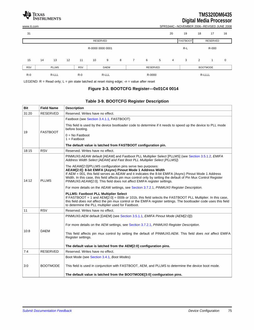
TMS320DM6435Digital Media Processor
www.ti.com SPRS344C–NOVEMBER 2006–REVISED JUNE 2008
31 20 19 18 17 16
RESERVED FASTBOOT RESERVED
R-0000 0000 0001 R-L R-000
15 14 13 12 11 10 9 8 7 6 5 4 3 2 1 0
RSV PLLMS RSV DAEM RESERVED BOOTMODE
R-0 R-LLL R-0 R-LLL R-0000 R-LLLL
LEGEND: R = Read only; L = pin state latched at reset rising edge; -n = value after reset
Figure 3-3. BOOTCFG Register—0x01C4 0014
Table 3-9. BOOTCFG Register DescriptionBit Field Name Description31:20 RESERVED Reserved. Writes have no effect.
Fastboot (see Section 3.4.1.1, FASTBOOT)
This field is used by the device bootloader code to determine if it needs to speed up the device to PLL modebefore booting.
19 FASTBOOT0 = No Fastboot1 = Fastboot
The default value is latched from FASTBOOT configuration pin.18:15 RSV Reserved. Writes have no effect.
PINMUX0.AEAW default [AEAW] and Fastboot PLL Multiplier Select [PLLMS] (see Section 3.5.1.2, EMIFAAddress Width Select [AEAW] and Fast Boot PLL Multiplier Select [PLLMS])
The AEAW[2:0]/PLLMS configuration pins serve two purposes:AEAW[2:0]: 8-bit EMIFA (Async) Pinout Mode 1 Address WidthIf AEM = 001, this field serves as AEAW and it indicates the 8-bit EMIFA (Async) Pinout Mode 1 AddressWidth. In this case, this field affects pin mux control only by setting the default of Pin Mux Control Register
14:12 PLLMS PINMUX0.AEAW[2:0]. This field does not affect EMIFA register settings.
For more details on the AEAW settings, see Section 3.7.2.1, PINMUX0 Register Description.
PLLMS: Fastboot PLL Multiplier SelectIf FASTBOOT = 1 and AEM[2:0] = 000b or 101b, this field selects the FASTBOOT PLL Multiplier. In this case,this field does not affect the pin mux control or the EMIFA register settings. The bootloader code uses this fieldto determine the PLL multiplier used for Fastboot.
11 RSV Reserved. Writes have no effect.PINMUX0.AEM default [DAEM] (see Section 3.5.1.1, EMIFA Pinout Mode (AEM[2:0]))
For more details on the AEM settings, see Section 3.7.2.1, PINMUX0 Register Description.
10:8 DAEMThis field affects pin mux control by setting the default of PINMUX0.AEM. This field does not affect EMIFARegister settings.
The default value is latched from the AEM[2:0] configuration pins.7:4 RESERVED Reserved. Writes have no effect.
Boot Mode (see Section 3.4.1, Boot Modes)
3:0 BOOTMODE This field is used in conjunction with FASTBOOT, AEM, and PLLMS to determine the device boot mode.
The default value is latched from the BOOTMODE[3:0] configuration pins.
Submit Documentation Feedback Device Configuration 75
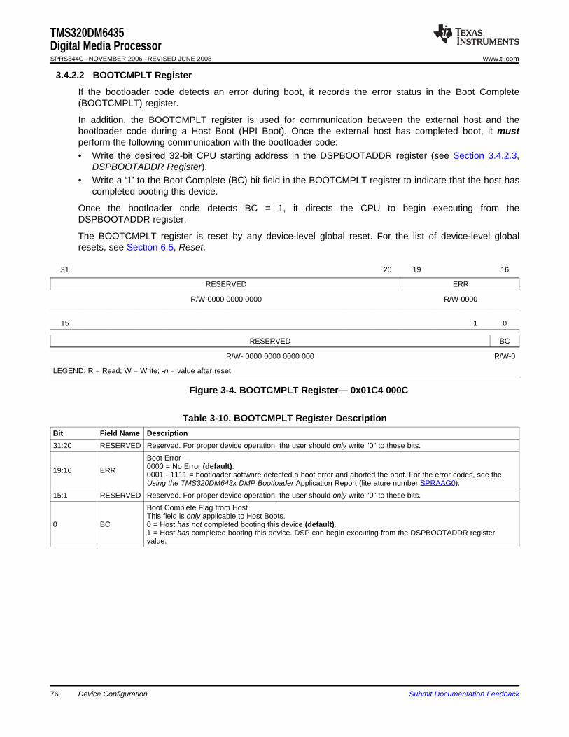
3.4.2.2 BOOTCMPLT Register
TMS320DM6435Digital Media ProcessorSPRS344C–NOVEMBER 2006–REVISED JUNE 2008 www.ti.com
If the bootloader code detects an error during boot, it records the error status in the Boot Complete(BOOTCMPLT) register.
In addition, the BOOTCMPLT register is used for communication between the external host and thebootloader code during a Host Boot (HPI Boot). Once the external host has completed boot, it mustperform the following communication with the bootloader code:• Write the desired 32-bit CPU starting address in the DSPBOOTADDR register (see Section 3.4.2.3,
DSPBOOTADDR Register).• Write a ‘1’ to the Boot Complete (BC) bit field in the BOOTCMPLT register to indicate that the host has
completed booting this device.
Once the bootloader code detects BC = 1, it directs the CPU to begin executing from theDSPBOOTADDR register.
The BOOTCMPLT register is reset by any device-level global reset. For the list of device-level globalresets, see Section 6.5, Reset.
31 20 19 16
RESERVED ERR
R/W-0000 0000 0000 R/W-0000
15 1 0
RESERVED BC
R/W- 0000 0000 0000 000 R/W-0
LEGEND: R = Read; W = Write; -n = value after reset
Figure 3-4. BOOTCMPLT Register— 0x01C4 000C
Table 3-10. BOOTCMPLT Register DescriptionBit Field Name Description31:20 RESERVED Reserved. For proper device operation, the user should only write "0" to these bits.
Boot Error0000 = No Error (default).19:16 ERR 0001 - 1111 = bootloader software detected a boot error and aborted the boot. For the error codes, see theUsing the TMS320DM643x DMP Bootloader Application Report (literature number SPRAAG0).
15:1 RESERVED Reserved. For proper device operation, the user should only write "0" to these bits.Boot Complete Flag from HostThis field is only applicable to Host Boots.
0 BC 0 = Host has not completed booting this device (default).1 = Host has completed booting this device. DSP can begin executing from the DSPBOOTADDR registervalue.
Device Configuration76 Submit Documentation Feedback
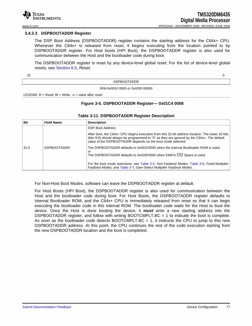
3.4.2.3 DSPBOOTADDR Register
TMS320DM6435Digital Media Processor
www.ti.com SPRS344C–NOVEMBER 2006–REVISED JUNE 2008
The DSP Boot Address (DSPBOOTADDR) register contains the starting address for the C64x+ CPU.Whenever the C64x+ is released from reset, it begins executing from the location pointed to byDSPBOOTADDR register. For Host boots (HPI Boot), the DSPBOOTADDR register is also used forcommunication between the Host and the bootloader code during boot.
The DSPBOOTADDR register is reset by any device-level global reset. For the list of device-level globalresets, see Section 6.5, Reset.
31 0
DSPBOOTADDR
R/W-0x0010 0000 or 0x4200 00000
LEGEND: R = Read; W = Write; -n = value after reset
Figure 3-5. DSPBOOTADDR Register— 0x01C4 0008
Table 3-11. DSPBOOTADDR Register DescriptionBit Field Name Description
DSP Boot Address
After boot, the C64x+ CPU begins execution from this 32-bit address location. The lower 10 bits(bits 9:0) should always be programmed to "0" as they are ignored by the C64x+. The defaultvalue of the DSPBOOTADDR depends on the boot mode selected.
31:0 DSPBOOTADDR The DSPBOOTADDR defaults to 0x00100000 when the Internal Bootloader ROM is used.orThe DSPBOOTADDR defaults to 0x42000000 when EMIFA CS2 Space is used.
For the boot mode selections, see Table 3-5, Non-Fastboot Modes; Table 3-6, Fixed-MultiplierFastboot Modes; and Table 3-7, User-Select Multiplier Fastboot Modes.
For Non-Host Boot Modes, software can leave the DSPBOOTADDR register at default.
For Host Boots (HPI Boot), the DSPBOOTADDR register is also used for communication between theHost and the bootloader code during boot. For Host Boots, the DSPBOOTADDR register defaults toInternal Bootloader ROM, and the C64x+ CPU is immediately released from reset so that it can beginexecuting the bootloader code in this internal ROM. The bootloader code waits for the Host to boot thedevice. Once the Host is done booting the device, it must write a new starting address into theDSPBOOTADDR register, and follow with writing BOOTCMPLT.BC = 1 to indicate the boot is complete.As soon as the bootloader code detects BOOTCMPLT.BC = 1, it instructs the CPU to jump to this newDSPBOOTADDR address. At this point, the CPU continues the rest of the code execution starting fromthe new DSPBOOTADDR location and the boot is completed.
Submit Documentation Feedback Device Configuration 77
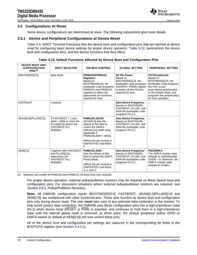
3.5 Configurations At Reset
3.5.1 Device and Peripheral Configurations at Device Reset
TMS320DM6435Digital Media ProcessorSPRS344C–NOVEMBER 2006–REVISED JUNE 2008 www.ti.com
Some device configurations are determined at reset. The following subsections give more details.
Table 2-5, BOOT Terminal Functions lists the device boot and configuration pins that are latched at devicereset for configuring basic device settings for proper device operation. Table 3-12, summarizes the deviceboot and configuration pins, and the device functions that they affect.
Table 3-12. Default Functions Affected by Device Boot and Configuration PinsDEVICE BOOT ANDCONFIGURATION BOOT SELECTED PIN MUX CONTROL GLOBAL SETTING PERIPHERAL SETTING
PINS (1)
BOOTMODE[3:0] Boot Mode PINMUX0/PINMUX1 I/O Pin Power: PSC/Peripherals:Registers: Based on Based onBased on BOOTMODE[3:0], the BOOTMODE[3:0], theBOOTMODE[3:0], the bootloader code programs bootloader code programsbootloader code programs VDD3P3V_PWDN register the PSC to putPINMUX0 and PINMUX1 to power up the I/O pins boot-related peripheral(s)registers to select the required for boot. in the Enable State, andappropriate pin functions programs the peripheral(s)required for boot. for boot operation.
FASTBOOT Fastboot – Sets Device Frequency: –Based on BOOTMODE,FASTBOOT, PLLMS, andAEM the bootloader codeprograms PLLC1.
AEAW[2:0]/PLLMS[2:0] If FASTBOOT = 1 and PINMUX0.AEAW: Sets Device Frequency: –AEM = 000b or 101b the AEAW[2:0] sets the Based on BOOTMODE,PLLMS[2:0] selects the default of this field to FASTBOOT, PLLMS, andFASTBOOT PLL control the EMIFA AEM the bootloader codeMultiplier. address bus width (only programs PLLC1.
applicable ifPINMUX0.AEM = 001b).
Affects the pin muxing inEMIFA/VPSS Sub-Block0.
AEM[2:0] Together with FASTBOOT PINMUX0.AEM: Sets Device Frequency: PSC/EMIFA:and PLLMS[2:0] , Sets the default of this Based on BOOTMODE, The EMIFA module statedetermines the field to control the EMIFA FASTBOOT, PLLMS, and defaults to SwRstDisableFASTBOOT PLL Pinout Mode. AEM the bootloader code if AEM = 0; otherwise, theMultiplier. programs PLLC1. EMIFA module state
Affects the pin muxing in defaults to Enable.EMIFA/VPSS Sub-Block0, 1, and 3.
(1) Software can modify all PINMUX0 and PINMUX1 bit fields from their defaults.
For proper device operation, external pullup/pulldown resistors may be required on these device boot andconfiguration pins. For discussion situations where external pullup/pulldown resistors are required, seeSection 3.9.1, Pullup/Pulldown Resistors.
Note: All DM6435 configuration inputs (BOOTMODE[3:0], FASTBOOT, AEAW[2:0]/PLLMS[2:0] andAEM[2:0]) are multiplexed with other functional pins. These pins function as device boot and configurationpins only during device reset. The user must take care of any potential data contention in the system. Tohelp avoid system data contention, the DM6435 puts these configuration pins into a high-impedance state(Hi-Z) when device reset (RESET or POR) is asserted, and continues to hold them in a high-impedancestate until the internal global reset is removed; at which point, the default peripheral (either GPIO orEMIFA based on default of AEM[2:0]) will now control these pins.
All of the device boot and configuration pin settings are captured in the corresponding bit fields in theBOOTCFG register (see Section 3.4.2.1).
Device Configuration78 Submit Documentation Feedback
3.5.1.1 EMIFA Pinout Mode (AEM[2:0])
3.5.1.2 EMIFA Address Width Select (AEAW) and FASTBOOT PLL Multiplier Select (PLLMS)
TMS320DM6435Digital Media Processor
www.ti.com SPRS344C–NOVEMBER 2006–REVISED JUNE 2008
The following subsections provide more details on the device configurations determined at device reset:AEM and AEAW/PLLMS.
To support different usage scenarios, the DM6435 provides intricate pin multiplexing between the EMIFAand other peripherals. The PINMUX0.AEM register bit field in the System Module determines the EMIFAPinout Mode. The AEM[2:0] pins only select the default EMIFA Pinout Mode. It is latched at device resetde-assertion (high) into the BOOTCFG.DAEM bit field. The AEM[2:0] value also sets the default of thePINMUX0.AEM bit field. While the BOOTCFG.DAEM bit field shows the actual latched value and cannotbe modified, the PINMUX0.AEM value can be changed by software to modify the EMIFA Pinout Mode.
Note: The AEM[2:0] value does not affect the operation of the EMIFA module itself. It only affects whichEMIFA pins are brought out to the device pins. For more details on the AEM settings, see Section 3.7,Multiplexed Pin Configurations.
In addition, for Fastboot modes (FASTBOOT = 1), the bootloader code determines the PLL1 multiplierbased on the default settings of AEM[2:0] and PLLMS[2:0]. For more details, see Section 3.4.1.1,Fastboot, and Section 3.5.1.2, EMIFA Address Width Select (AEAW) and FASTBOOT PLL MultiplierSelect (PLLMS).
The AEAW[2:0]/PLLMS[2:0] pins serve two functional purposes (AEAW or PLLMS), depending on theFASTBOOT and AEM settings. The AEAW[2:0]/PLLMS[2:0] pins are latched at device reset de-assertion(high) and captured in the BOOTCFG.PLLMS bit field. This value also sets the default of thePINMUX0.AEAW field.
While the BOOTCFG.PLLMS field shows the actual latched value and cannot be modified, thePINMUX0.AEAW value can be changed by software to modify the EMIFA pinout.
AEAW as EMIFA Address Width Select (AEAW)
If AEM[2:0] = 001b [8-bit EMIFA (Async) Pinout Mode 1], the AEAW[2:0]/PLLMS[2:0] pins serve as AEAWto set the default of the EMIFA Address Width Selection.
When EMIFA is used in the 8-bit EMIFA (Async) Pinout Mode 1 (PINMUX0.AEM = 001b), the user has theoption to determine how many address pins are needed. The unused address pins can be used asgeneral-purpose input/output (GPIO) pins or extra data pins for VPFE. For more details on how the AEAWsettings control the exact pin out when AEM = 001b, see Section 3.7.3.11, EMIFA/VPSS Block Muxing.For other EMIFA Pinout Modes (AEM not 001b), AEAW is not applicable in determining the EMIFAaddress width.
Note: AEAW[2:0] value does not affect the operation of the EMIFA module itself. It only affects which ofthe EMIFA address bits are brought out to the device pins.
AEAW as Fast Boot PLL Multiplier Select (PLLMS)
If FASTBOOT = 1, and AEM[2:0] = 000b [No EMIFA] or 101b [8-bit EMIFA (NAND) Pinout Mode 5], theAEAW[2:0]/PLLMS[2:0] pins serve as PLLMS to select PLL multiplier for Fastboot modes.
For more information on boot modes and the FASTBOOT PLL multiplier selection, see Section 3.4.1, BootModes.
Submit Documentation Feedback Device Configuration 79
3.6 Configurations After Reset
3.6.1 Switch Central Resource (SCR) Bus Priorities
TMS320DM6435Digital Media ProcessorSPRS344C–NOVEMBER 2006–REVISED JUNE 2008 www.ti.com
The following sections provide details on configuring the device after reset.
Multiplexed pins are configured both at and after reset. Section 3.5.1, Device and PeripheralConfigurations at Device Reset, discusses multiplexed pin control at reset. For more details on multiplexedpins control after reset, see Section 3.7 , Multiplexed Pin Configurations.
Prioritization within the Switched Central Resource (SCR) is programmable for each master. The registerbit fields and default priority levels for DM6435 bus masters are shown in Table 3-13, DM6435 Default BusMaster Priorities. The priority levels should be tuned to obtain the best system performance for a particularapplication. Lower values indicate higher priority. For most masters, their priority values are programmedat the system level by configuring the MSTPRI0 and MSTPRI1 registers. Details on the MSTPRI0/1registers are shown in Figure 3-6 and Figure 3-7. The C64x+, VPSS, and EDMA masters contain registersthat control their own priority values.
Table 3-13. DM6435 Default Bus Master PrioritiesPriority Bit Field Bus Master Default Priority Level
VPSSP VPSS 0 (VPSS PCR Register)EDMATC0P EDMATC0 0 (EDMACC QUEPRI Register)EDMATC1P EDMATC1 0 (EDMACC QUEPRI Register)EDMATC2P EDMATC2 0 (EDMACC QUEPRI Register)
C64X+_DMAP C64X+ (DMA) 7 (C64x + MDMAARBE.PRI field)C64X+_CFGP C64X+ (CFG) 1 (MSTPRI0 Register)
EMACP EMAC 4 (MSTPRI1 Register)VLYNQP VLYNQ 4 (MSTPRI1 Register)
HPIP HPI 4 (MSTPRI1 Register)
31 16
RESERVED
R-0000 0000 0000 0000
15 11 10 9 8 7 0
RESERVED C64X+_CFGP RESERVED
R-0000 0 R/W-001 R-0000 0000
LEGEND: R = Read; W = Write; -n = value after reset
Figure 3-6. MSTPRI0 Register— 0x01C4 003C
Device Configuration80 Submit Documentation Feedback
TMS320DM6435Digital Media Processor
www.ti.com SPRS344C–NOVEMBER 2006–REVISED JUNE 2008
Table 3-14. MSTPRI0 Register DescriptionBit Field Name Description31:11 RESERVED Reserved. Read-only, writes have no effect.
C64X+_CFG master port priority in System Infrastructure.000 = Priority 0 (Highest) 100 = Priority 4
10:8 C64X+_CFGP 001 = Priority 1 101 = Priority 5010 = Priority 2 110 = Priority 6011 = Priority 3 111 = Priority 7 (Lowest)
7:0 RESERVED Reserved. Read-only, writes have no effect.
31 27 26 25 24 23 22 21 20 19 18 17 16
RESERVED RSV RSV HPIP RSV VLYNQP
R-0000 0 R/W-100 R-0 R/W-100 R-0 R/W-100
15 3 2 1 0
RESERVED EMACP
R- 0000 0000 0000 0 R/W-100
LEGEND: R = Read; W = Write; -n = value after reset
Figure 3-7. MSTPRI1 Register— 0x01C4 0040
Table 3-15. MSTPRI1 Register DescriptionBit Field Name Description31:27 RESERVED Reserved. Read-only, writes have no effect.
Reserved. For proper device operation, the user must only write "100" to26:24 RSV these bits.23 RSV Reserved. Read-only, writes have no effect.
HPI master port priority in System Infrastructure.000 = Priority 0 (Highest) 100 = Priority 4
22:20 HPIP 001 = Priority 1 101 = Priority 5010 = Priority 2 110 = Priority 6011 = Priority 3 111 = Priority 7 (Lowest)
19 RSV Reserved. Read-only, writes have no effect.VLYNQ master port priority in System Infrastructure.000 = Priority 0 (Highest) 100 = Priority 4
18:16 VLYNQP 001 = Priority 1 101 = Priority 5010 = Priority 2 110 = Priority 6011 = Priority 3 111 = Priority 7 (Lowest)
15:3 RESERVED Reserved. Read-only, writes have no effect.EMAC master port priority in System Infrastructure.000 = Priority 0 (Highest) 100 = Priority 4
2:0 EMACP 001 = Priority 1 101 = Priority 5010 = Priority 2 110 = Priority 6011 = Priority 3 111 = Priority 7 (Lowest)
Submit Documentation Feedback Device Configuration 81
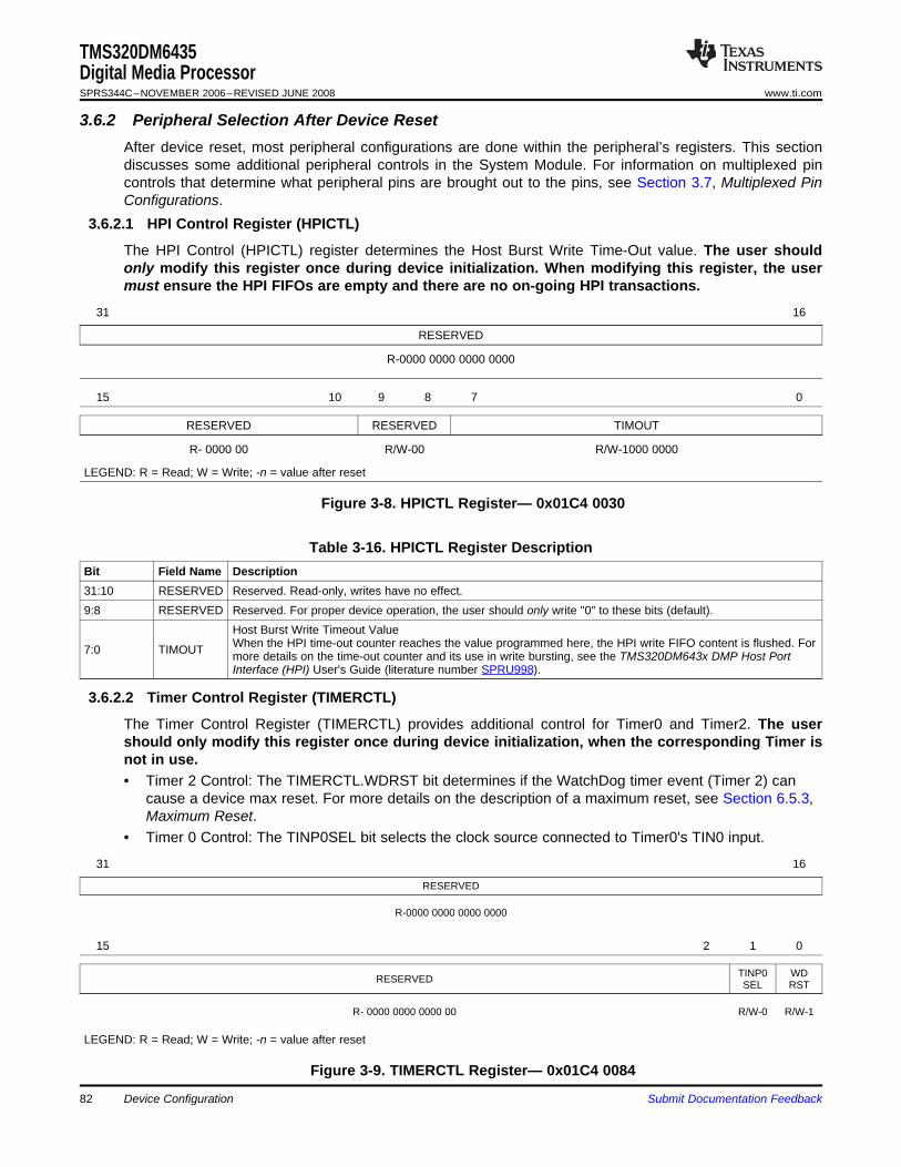
3.6.2 Peripheral Selection After Device Reset
3.6.2.1 HPI Control Register (HPICTL)
3.6.2.2 Timer Control Register (TIMERCTL)
TMS320DM6435Digital Media ProcessorSPRS344C–NOVEMBER 2006–REVISED JUNE 2008 www.ti.com
After device reset, most peripheral configurations are done within the peripheral’s registers. This sectiondiscusses some additional peripheral controls in the System Module. For information on multiplexed pincontrols that determine what peripheral pins are brought out to the pins, see Section 3.7, Multiplexed PinConfigurations.
The HPI Control (HPICTL) register determines the Host Burst Write Time-Out value. The user shouldonly modify this register once during device initialization. When modifying this register, the usermust ensure the HPI FIFOs are empty and there are no on-going HPI transactions.
31 16
RESERVED
R-0000 0000 0000 0000
15 10 9 8 7 0
RESERVED RESERVED TIMOUT
R- 0000 00 R/W-00 R/W-1000 0000
LEGEND: R = Read; W = Write; -n = value after reset
Figure 3-8. HPICTL Register— 0x01C4 0030
Table 3-16. HPICTL Register DescriptionBit Field Name Description31:10 RESERVED Reserved. Read-only, writes have no effect.9:8 RESERVED Reserved. For proper device operation, the user should only write "0" to these bits (default).
Host Burst Write Timeout ValueWhen the HPI time-out counter reaches the value programmed here, the HPI write FIFO content is flushed. For7:0 TIMOUT more details on the time-out counter and its use in write bursting, see the TMS320DM643x DMP Host PortInterface (HPI) User's Guide (literature number SPRU998).
The Timer Control Register (TIMERCTL) provides additional control for Timer0 and Timer2. The usershould only modify this register once during device initialization, when the corresponding Timer isnot in use.• Timer 2 Control: The TIMERCTL.WDRST bit determines if the WatchDog timer event (Timer 2) can
cause a device max reset. For more details on the description of a maximum reset, see Section 6.5.3,Maximum Reset.
• Timer 0 Control: The TINP0SEL bit selects the clock source connected to Timer0's TIN0 input.
31 16
RESERVED
R-0000 0000 0000 0000
15 2 1 0
TINP0 WDRESERVED SEL RST
R- 0000 0000 0000 00 R/W-0 R/W-1
LEGEND: R = Read; W = Write; -n = value after reset
Figure 3-9. TIMERCTL Register— 0x01C4 0084
Device Configuration82 Submit Documentation Feedback
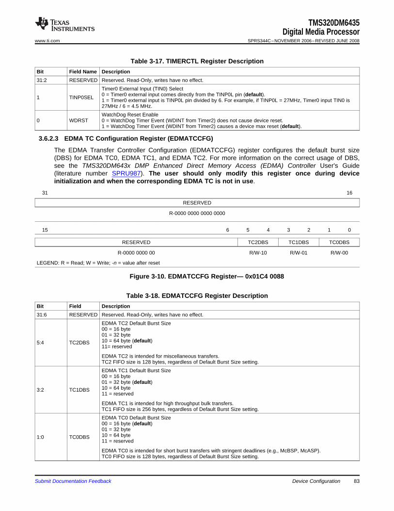
3.6.2.3 EDMA TC Configuration Register (EDMATCCFG)
TMS320DM6435Digital Media Processor
www.ti.com SPRS344C–NOVEMBER 2006–REVISED JUNE 2008
Table 3-17. TIMERCTL Register DescriptionBit Field Name Description31:2 RESERVED Reserved. Read-Only, writes have no effect.
Timer0 External Input (TIN0) Select0 = Timer0 external input comes directly from the TINP0L pin (default).1 TINP0SEL 1 = Timer0 external input is TINP0L pin divided by 6. For example, if TINP0L = 27MHz, Timer0 input TIN0 is27MHz / 6 = 4.5 MHz.WatchDog Reset Enable
0 WDRST 0 = WatchDog Timer Event (WDINT from Timer2) does not cause device reset.1 = WatchDog Timer Event (WDINT from Timer2) causes a device max reset (default).
The EDMA Transfer Controller Configuration (EDMATCCFG) register configures the default burst size(DBS) for EDMA TC0, EDMA TC1, and EDMA TC2. For more information on the correct usage of DBS,see the TMS320DM643x DMP Enhanced Direct Memory Access (EDMA) Controller User's Guide(literature number SPRU987). The user should only modify this register once during deviceinitialization and when the corresponding EDMA TC is not in use.
31 16
RESERVED
R-0000 0000 0000 0000
15 6 5 4 3 2 1 0
RESERVED TC2DBS TC1DBS TC0DBS
R-0000 0000 00 R/W-10 R/W-01 R/W-00
LEGEND: R = Read; W = Write; -n = value after reset
Figure 3-10. EDMATCCFG Register— 0x01C4 0088
Table 3-18. EDMATCCFG Register DescriptionBit Field Description31:6 RESERVED Reserved. Read-Only, writes have no effect.
EDMA TC2 Default Burst Size00 = 16 byte01 = 32 byte10 = 64 byte (default)5:4 TC2DBS11= reserved
EDMA TC2 is intended for miscellaneous transfers.TC2 FIFO size is 128 bytes, regardless of Default Burst Size setting.EDMA TC1 Default Burst Size00 = 16 byte01 = 32 byte (default)10 = 64 byte3:2 TC1DBS11 = reserved
EDMA TC1 is intended for high throughput bulk transfers.TC1 FIFO size is 256 bytes, regardless of Default Burst Size setting.EDMA TC0 Default Burst Size00 = 16 byte (default)01 = 32 byte10 = 64 byte1:0 TC0DBS11 = reserved
EDMA TC0 is intended for short burst transfers with stringent deadlines (e.g., McBSP, McASP).TC0 FIFO size is 128 bytes, regardless of Default Burst Size setting.
Submit Documentation Feedback Device Configuration 83
3.7 Multiplexed Pin Configurations
TMS320DM6435Digital Media ProcessorSPRS344C–NOVEMBER 2006–REVISED JUNE 2008 www.ti.com
DM6435 makes extensive use of pin multiplexing to accommodate a large number of peripheral functionsin the smallest possible package, providing ultimate flexibility for end applications.
The Pin Multiplex Registers PINMUX0 and PINMUX1 in the System Module are responsible for controllingall pin multiplexing functions on the DM6435. The default setting of some of the PINMUX0 and PINMUX1bit fields are configured by configuration pins latched at reset (see Section 3.5.1, Device and PeripheralConfigurations at Device Reset). After reset, software may program the PINMUX0 and PINMUX1 registersto switch pin functionalities.
The following peripherals have multiplexed pins: VPSS (VPFE), EMIFA, HPI, VLYNQ, EMAC, McASP0,McBSP0, PWM0, PWM1, PWM2, Timer0, Timer1, UART0, UART1, HECC, and GPIO.
The device is divided into the following Pin Multiplexed Blocks (Pin Mux Blocks):• EMIFA/VPSS Block: VPSS (VPFE), EMIFA, and GPIO. This block is further subdivided into these
sub-blocks:– Sub-Block 0: VPFE (CCDC), part of EMIFA (address and control), and GPIO– Sub-Block 1: part of EMIFA (data, address, control), and GPIO– Sub-Block 2: part of EMIFA (control signals EM_WAIT/(RDY/BSY), EM_OE, and EM_WE)– Sub-Block 3: part of EMIFA (address EM_A[12:5]), and GPIO
• Host Block: HPI, VLYNQ, EMAC, and GPIO• Serial Port Block: McBSP0, McASP0, and GPIO. This block is further sub-divided into sub-blocks.
– Serial Port Sub-Block 0: McBSP0, part of McASP0, and GPIO– Serial Port Sub-Block 1: part of McASP0 and GPIO
• UART0 Flow Control Block: UART0 flow control, PWM0, and GPIO• UART0 Data Block: UART0 data and GPIO• Timer0 Block: Timer0 and McBSP0 CLKS pins• Timer1 Block: Timer1 and HECC, UART1 data• PWM1 Block: PWM1 and GPIO• CLKOUT Block: CLKOUT0, PWM2, and GPIO
As shown in the list above, the McBSP0 and UART0 peripherals span multiple Pin Mux Blocks. To usethese peripherals, they must be selected in all relevant Pin Mux Blocks. For more details, seeSection 3.7.3, Pin Multiplexing Details, and Section 3.7.3.2, Peripherals Spanning Multiple Pin MuxBlocks.
Note: there is no actual pin multiplexing in EMIFA/VPSS Sub-Block 2. However this is still considered a"pin mux block" because it contains part of the pins necessary for EMIFA.
A high level view of the Pin Mux Blocks is shown in Figure 3-11. In each Pin Mux Block, thePINMUX0/PINMUX1 default settings are underlined.
Note: some default pin functions are determined by configuration pins (AEAW[2:0] and AEM[2:0]);therefore, more than one configuration setting can serve as default based on the configuration pin settingslatched at device reset.
84 Device Configuration Submit Documentation Feedback
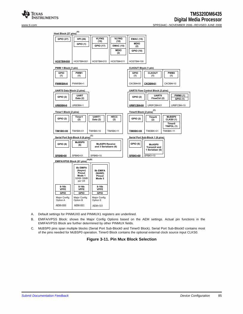
Host Block (27 pins)(A)
GPIO (27)
HOSTBK=000
VLYNQ(10)
GPIO (17)
VLYNQ(10)
EMAC (15)
MDIO(2)
HOSTBK=001 HOSTBK=010 HOSTBK=011 HOSTBK=100
HPI (26)
GPIO (1)
EMAC (15)
MDIO(2)
GPIO (10)
UART0 Data Block (2 pins)
GPIO (2)
UR0DBK=0
UARTData (2)
UR0DBK=1
UART0 Flow Control Block (2 pins)
GPIO (2)
UR0FCBK=00
UART0FlowCtrl (2)
UR0FCBK=01
PWM0 (1)
UR0FCBK=10
GPIO (1)
Timer1 Block (2 pins)
GPIO (2)
TIM1BK=00
Timer1(2)
TIM1BK=01
UART1Data (2)
TIM1BK=10
HECC(2)
TIM1BK=11
Timer0 Block (2 pins)(C)
GPIO (2)
TIM0BK=00
Timer0(2)
TIM0BK=01
McBSP0CLKS0 (1)
TIM0BK=11
Timer0TINPOL (1)
PWM 1 Block (1 pin)
GPIO(1)
PWM1BK=0
PWM1(1)
PWM1BK=1
CLKOUT Block (1 pin)
GPIO(1)
CKOBK=00
CLKOUT(1)
CKOBK=01
PWM2(1)
CKOBK=10
Serial Port Sub-Block 0 (6 pins)(C)
GPIO (6)
SPBK0=00
McBSP0(6)
SPBK0=01
McASP0 Receiveand 3 Serializers (6)
SPBK0=10
Serial Port Sub-Block 1 (6 pins)
GPIO (6)
SPBK1=00
McASP0Transmit and
1 Serializer (6)
SPBK1=10
EMIFA/VPSS Block (61 pins)(A)(B)
Major ConfigOption A
8-16bVPFE
GPIO
Major ConfigOption B
GPIO
8-16bVPFE
8b EMIFA(Async)PinoutMode 1
32KB-16MBper CE
Major ConfigOption E
GPIO
8-16bVPFE
8b EMIFA(NAND)PinoutMode 5
AEM=000 AEM=001 AEM=101
TMS320DM6435Digital Media Processor
www.ti.com SPRS344C–NOVEMBER 2006–REVISED JUNE 2008
A. Default settings for PINMUX0 and PINMUX1 registers are underlined.B. EMIFA/VPSS Block: shows the Major Config Options based on the AEM settings. Actual pin functions in the
EMIFA/VPSS Block are further determined by other PINMUX fields.C. McBSP0 pins span multiple blocks (Serial Port Sub-Block0 and Timer0 Block). Serial Port Sub-Block0 contains most
of the pins needed for McBSP0 operation. Timer0 Block contains the optional external clock source input CLKS0.
Figure 3-11. Pin Mux Block Selection
Submit Documentation Feedback Device Configuration 85
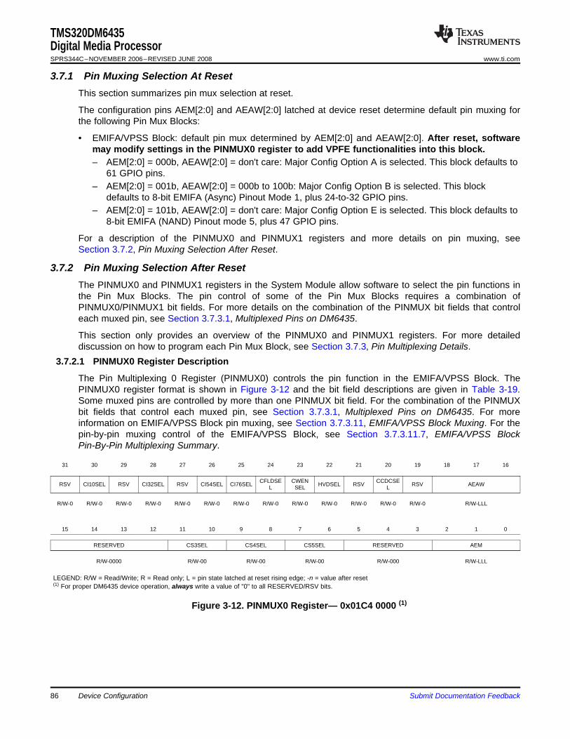
3.7.1 Pin Muxing Selection At Reset
3.7.2 Pin Muxing Selection After Reset
3.7.2.1 PINMUX0 Register Description
TMS320DM6435Digital Media ProcessorSPRS344C–NOVEMBER 2006–REVISED JUNE 2008 www.ti.com
This section summarizes pin mux selection at reset.
The configuration pins AEM[2:0] and AEAW[2:0] latched at device reset determine default pin muxing forthe following Pin Mux Blocks:
• EMIFA/VPSS Block: default pin mux determined by AEM[2:0] and AEAW[2:0]. After reset, softwaremay modify settings in the PINMUX0 register to add VPFE functionalities into this block.– AEM[2:0] = 000b, AEAW[2:0] = don't care: Major Config Option A is selected. This block defaults to
61 GPIO pins.– AEM[2:0] = 001b, AEAW[2:0] = 000b to 100b: Major Config Option B is selected. This block
defaults to 8-bit EMIFA (Async) Pinout Mode 1, plus 24-to-32 GPIO pins.– AEM[2:0] = 101b, AEAW[2:0] = don't care: Major Config Option E is selected. This block defaults to
8-bit EMIFA (NAND) Pinout mode 5, plus 47 GPIO pins.
For a description of the PINMUX0 and PINMUX1 registers and more details on pin muxing, seeSection 3.7.2, Pin Muxing Selection After Reset.
The PINMUX0 and PINMUX1 registers in the System Module allow software to select the pin functions inthe Pin Mux Blocks. The pin control of some of the Pin Mux Blocks requires a combination ofPINMUX0/PINMUX1 bit fields. For more details on the combination of the PINMUX bit fields that controleach muxed pin, see Section 3.7.3.1, Multiplexed Pins on DM6435.
This section only provides an overview of the PINMUX0 and PINMUX1 registers. For more detaileddiscussion on how to program each Pin Mux Block, see Section 3.7.3, Pin Multiplexing Details.
The Pin Multiplexing 0 Register (PINMUX0) controls the pin function in the EMIFA/VPSS Block. ThePINMUX0 register format is shown in Figure 3-12 and the bit field descriptions are given in Table 3-19.Some muxed pins are controlled by more than one PINMUX bit field. For the combination of the PINMUXbit fields that control each muxed pin, see Section 3.7.3.1, Multiplexed Pins on DM6435. For moreinformation on EMIFA/VPSS Block pin muxing, see Section 3.7.3.11, EMIFA/VPSS Block Muxing. For thepin-by-pin muxing control of the EMIFA/VPSS Block, see Section 3.7.3.11.7, EMIFA/VPSS BlockPin-By-Pin Multiplexing Summary.
31 30 29 28 27 26 25 24 23 22 21 20 19 18 17 16
CFLDSE CWEN CCDCSERSV CI10SEL RSV CI32SEL RSV CI54SEL CI76SEL HVDSEL RSV RSV AEAWL SEL L
R/W-0 R/W-0 R/W-0 R/W-0 R/W-0 R/W-0 R/W-0 R/W-0 R/W-0 R/W-0 R/W-0 R/W-0 R/W-0 R/W-LLL
15 14 13 12 11 10 9 8 7 6 5 4 3 2 1 0
RESERVED CS3SEL CS4SEL CS5SEL RESERVED AEM
R/W-0000 R/W-00 R/W-00 R/W-00 R/W-000 R/W-LLL
LEGEND: R/W = Read/Write; R = Read only; L = pin state latched at reset rising edge; -n = value after reset(1) For proper DM6435 device operation, always write a value of "0" to all RESERVED/RSV bits.
Figure 3-12. PINMUX0 Register— 0x01C4 0000 (1)
Device Configuration86 Submit Documentation Feedback

TMS320DM6435Digital Media Processor
www.ti.com SPRS344C–NOVEMBER 2006–REVISED JUNE 2008
Table 3-19. PINMUX0 Register DescriptionBit Field Name Description Pins Controlled
Reserved. For proper device operation, the user should only write "0" to this bit31 RSV (default).
Sub-Block 0CI[1:0] Function Select.CI1(CCD9)/EM_A[19]/GP[45]0 = No CCDC CI[1:0].
Pins function as GPIO or EMIFA based on AEM and AEAW settings (default). CI0(CCD8)/EM_A[20]/GP[44]30 CI10SEL1 = Selects CCDC [1:0] (as CCD8 and CCD9, respectively) to get at least a 10-bit The combination of PINMUX0 fields AEM,CCDC. AEAW, and CI10SEL bits control the pinTo use the 10-bit CCDC, the user must also configure PINMUX0.CCDCSEL = 1. muxing of these 2 pins. (1)
Reserved. For proper device operation, the user should only write "0" to this bit29 RSV (default).
CI[3:2] Function Select. Sub-Block 0
0 = No CCDC CI[3:2]. CI3(CCD11)/EM_A[17]/GP[47]Pins function as GPIO or EMIFA based on AEM and AEAW settings (default).
CI2(CCD10)/EM_A[18]/GP[46]28 CI32SEL1 = Selects CCDC [3:2] (as CCD10 and CCD11, respectively) to get at least a
The combination of PINMUX0 fields AEM,12-bit CCDC.AEAW, and CI32SEL bits control the pinTo use the 12-bit CCDC, the user must also configure PINMUX0.CCDCSEL = 1muxing of these 2 pins. (1)and PINMUX0.CI10SEL = 1.
Reserved. For proper device operation, the user should only write "0" to this bit27 RSV (default).
CI[5:4] Function Select. Sub-Block 0
0 = No CCDC CI[5:4]. CI5(CCD13)/EM_A[15]/GP[49]Pins function as GPIO or EMIFA based on AEM and AEAW settings (default).
CI4(CCD12)/EM_A[16]/GP[48]26 CI54SEL1 = Selects CCDC [5:4] (as CCD12 and CCD13, respectively) to get at least a
The combination of PINMUX0 fields AEM,14-bit CCDC.AEAW, and CI54SEL bits control the pinTo use the 14-bit CCDC, the user must also configure PINMUX0.CCDCSEL = 1,muxing of these 2 pins. (1)PINMUX0.CI10SEL = 1, and PINMUX0.CI32SEL = 1.
CI[7:6] Function Select. Sub-Block 0
0 = No CCDC CI[7:6]. CI7(CCD15)/EM_A[13]/GP[51]Pins function as GPIO or EMIFA based on AEM and AEAW settings (default).
CI6(CCD14)/EM_A[14]/GP[50]25 CI76SEL1 = Selects CCDC [7:6] (as CCD14 and CCD15, respectively) to get at least a
The combination of PINMUX0 fields AEM,16-bit CCDC.AEAW, and CI76SEL bits control the pinTo use the 16-bit CCDC, the user must also configure PINMUX0.CCDCSEL = 1,muxing of these 2 pins. (1)PINMUX0.CI10SEL = 1, PINMUX0.CI32SEL = 1, and PINMUX0.CI54SEL = 1.
Sub-Block 0CCDC Field Select.C_FIELD/EM_A[21]/GP[34]0 = No CCDC Field (C_FIELD).24 CFLDSEL Pin functions as EMIFA EM_A[21] or GPIO based on AEM setting (default). The combination of PINMUX0/1 fieldsCFLDSEL and AEM control the muxing of this1 = CCDC Field (C_FIELD). pin. (1)
CCDC Write Enable Select.Sub-Block 0
0 = No CCDC Write Enable.Pin functions as EMIFA EM_R/W or GPIO based on AEM setting (default). C_WE/EM_R/W/GP[35]23 CWENSEL1 = CCDC Write Enable (C_WE). The combination of PINMUX0 fields CWENSELPin functions as CCDC Write Enable C_WE. and AEM control the muxing of this pin. (1)
Applicable only for AEM = 0 (000b) or 5 (101b).
Sub-Block 0CCDC HD and VD Select.VD/GP[53]0 = No CCDC HD and VD.22 HVDSEL HD/GP[52]Pins function as GPIO (GP[53] and GP[52]) (default).The PINMUX0 field HVDSEL alone controls the1 = CCDC HD and VD. muxing of these 2 pins.
Reserved. For proper device operation, the user should only write "0" to this bit21 RSV (default).
(1) For the full set of valid configurations of these pins, see Section 3.7.3.11.7, EMIFA/VPSS Block Pin-By-Pin Multiplexing Summary.
Submit Documentation Feedback Device Configuration 87
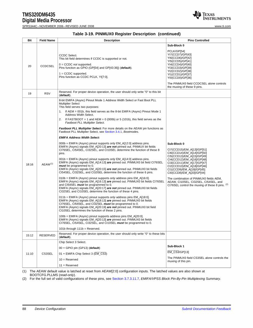
TMS320DM6435Digital Media ProcessorSPRS344C–NOVEMBER 2006–REVISED JUNE 2008 www.ti.com
Table 3-19. PINMUX0 Register Description (continued)Bit Field Name Description Pins Controlled
Sub-Block 0
PCLK/GP[54]YI7(CCD7)/GP[43]CCDC Select.YI6(CCD6)/GP[42]This bit field determines if CCDC is supported or not.YI5(CCD5)/GP[41]
0 = CCDC not supported. YI4(CCD4)/GP[40]20 CCDCSEL Pins function as GPIO (GP[54] and GP[43:36]) (default). YI3(CCD3)/GP[39]YI2(CCD2)/GP[38]
1 = CCDC supported. YI1(CCD1)/GP[37]Pins function as CCDC PCLK, YI[7:0]. YI0(CCD0)/GP[36]
The PINMUX0 field CCDCSEL alone controlsthe muxing of these 9 pins.
Reserved. For proper device operation, the user should only write "0" to this bit19 RSV (default).
8-bit EMIFA (Async) Pinout Mode 1 Address Width Select or Fast Boot PLLMultiplier SelectThis field serves two purposes:1. If AEM = 001b, this field serves as the 8-bit EMIFA (Async) Pinout Mode 1
Address Width Select.2. If FASTBOOT = 1 and AEM = 0 (000b) or 5 (101b), this field serves as the
Fastboot PLL Multiplier Select.
Fastboot PLL Multiplier Select: For more details on the AEAW pin functions asFastboot PLL Multiplier Select, see Section 3.4.1, Bootmodes.
EMIFA Address Width Select:
000b = EMIFA (Async) pinout supports only EM_A[12:0] address pins. Sub-Block 0EMIFA (Async) signals EM_A[20:13] are not pinned out. PINMUX bit fields
CI7(CCD15)/EM_A[13]/GP[51]CI76SEL, CI54SEL, CI32SEL, and CI10SEL determine the function of these 8CI6(CCD14)/EM_A[14]/GP[50]pins.CI5(CCD13)/EM_A[15]/GP[49]
001b = EMIFA (Async) pinout supports only EM_A[14:0] address pins. CI4(CCD12)/EM_A[16]/GP[48]EMIFA (Async) signals EM_A[14:13] are pinned out. PINMUX0 bit field CI76SEL CI3(CCD11)/EM_A[17]/GP[47]18:16 AEAW (1)must be programmed to 0. CI2(CCD10)/EM_A[18]/GP[46]EMIFA (Async) signals EM_A[20:15] are not pinned out. PINMUX0 bit fields CI1(CCD9)/EM_A[19]/GP[45]CI54SEL, CI32SEL, and CI10SEL determine the function of these 6 pins. CI0(CCD8)/EM_A[20]/GP[44]
010b = EMIFA (Async) pinout supports only address pins EM_A[16:0]. The combination of PINMUX0 fields AEM,EMIFA (Async) signals EM_A[16:13] are pinned out. PINMUX0 bit fields CI76SEL AEAW, CI10SEL, CI32SEL, CI54SEL, andand CI54SEL must be programmed to 0. CI76SEL control the muxing of these 8 pins. (2)
EMIFA (Async) signals EM_A[20:17] are not pinned out. PINMUX0 bit fieldsCI32SEL and CI10SEL determine the function of these 4 pins.
011b = EMIFA (Async) pinout supports only address pins EM_A[18:0].EMIFA (Async) signals EM_A[18:13] are pinned out. PINMUX0 bit fieldsCI76SEL, CI54SEL, and CI32SEL must be programmed to 0.EMIFA (Async) signals EM_A[20:19] are not pinned out. PINMUX0 bit fieldCI10SEL determines the function of these 2 pins.
100b = EMIFA (Async) pinout supports address pins EM_A[20:0].EMIFA (Async) signals EM_A[20:13] are pinned out. PINMUX0 bit fieldsCI76SEL, CI54SEL, CI32SEL, and CI10SEL must be programmed to 0.
101b through 111b = Reserved.
Reserved. For proper device operation, the user should only write "0" to these bits15:12 RESERVED (default).
Chip Select 3 Select.Sub-Block 100 = GPIO pin (GP13) (default)EM_CS3/GP[13]11:10 CS3SEL 01 = EMIFA Chip Select 3 (EM_CS3)The PINMUX0 field CS3SEL alone controls the10 = Reserved muxing of this pin.
11 = Reserved
(1) The AEAW default value is latched at reset from AEAW[2:0] configuration inputs. The latched values are also shown atBOOTCFG.PLLMS (read-only).
(2) For the full set of valid configurations of these pins, see Section 3.7.3.11.7, EMIFA/VPSS Block Pin-By-Pin Multiplexing Summary.
88 Device Configuration Submit Documentation Feedback
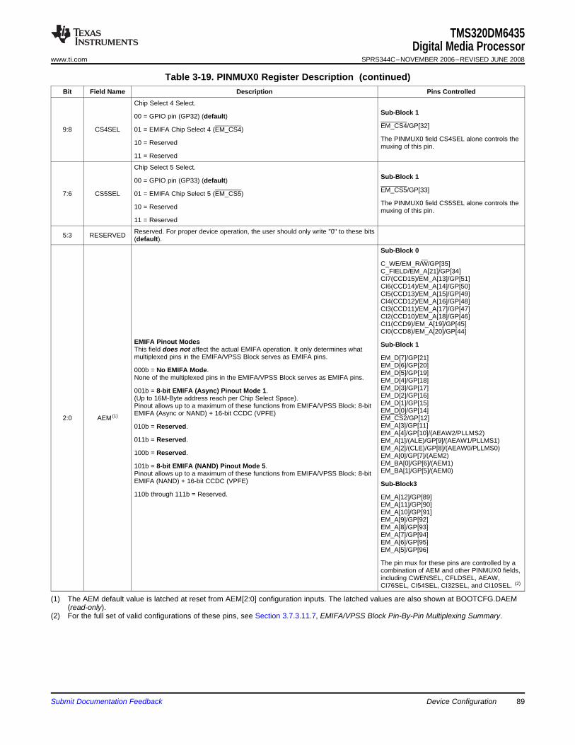
TMS320DM6435Digital Media Processor
www.ti.com SPRS344C–NOVEMBER 2006–REVISED JUNE 2008
Table 3-19. PINMUX0 Register Description (continued)Bit Field Name Description Pins Controlled
Chip Select 4 Select.Sub-Block 100 = GPIO pin (GP32) (default)EM_CS4/GP[32]9:8 CS4SEL 01 = EMIFA Chip Select 4 (EM_CS4)The PINMUX0 field CS4SEL alone controls the10 = Reserved muxing of this pin.
11 = Reserved
Chip Select 5 Select.Sub-Block 100 = GPIO pin (GP33) (default)EM_CS5/GP[33]7:6 CS5SEL 01 = EMIFA Chip Select 5 (EM_CS5)The PINMUX0 field CS5SEL alone controls the10 = Reserved muxing of this pin.
11 = Reserved
Reserved. For proper device operation, the user should only write "0" to these bits5:3 RESERVED (default).
Sub-Block 0
C_WE/EM_R/W/GP[35]C_FIELD/EM_A[21]/GP[34]CI7(CCD15)/EM_A[13]/GP[51]CI6(CCD14)/EM_A[14]/GP[50]CI5(CCD13)/EM_A[15]/GP[49]CI4(CCD12)/EM_A[16]/GP[48]CI3(CCD11)/EM_A[17]/GP[47]CI2(CCD10)/EM_A[18]/GP[46]CI1(CCD9)/EM_A[19]/GP[45]CI0(CCD8)/EM_A[20]/GP[44]
EMIFA Pinout Modes Sub-Block 1This field does not affect the actual EMIFA operation. It only determines whatmultiplexed pins in the EMIFA/VPSS Block serves as EMIFA pins. EM_D[7]/GP[21]
EM_D[6]/GP[20]000b = No EMIFA Mode. EM_D[5]/GP[19]None of the multiplexed pins in the EMIFA/VPSS Block serves as EMIFA pins. EM_D[4]/GP[18]
EM_D[3]/GP[17]001b = 8-bit EMIFA (Async) Pinout Mode 1.EM_D[2]/GP[16](Up to 16M-Byte address reach per Chip Select Space).EM_D[1]/GP[15]Pinout allows up to a maximum of these functions from EMIFA/VPSS Block: 8-bitEM_D[0]/GP[14]EMIFA (Async or NAND) + 16-bit CCDC (VPFE)
2:0 AEM (1) EM_CS2/GP[12]EM_A[3]/GP[11]010b = Reserved.EM_A[4]/GP[10]/(AEAW2/PLLMS2)
011b = Reserved. EM_A[1]/(ALE)/GP[9]/(AEAW1/PLLMS1)EM_A[2]/(CLE)/GP[8]/(AEAW0/PLLMS0)
100b = Reserved. EM_A[0]/GP[7]/(AEM2)EM_BA[0]/GP[6]/(AEM1)101b = 8-bit EMIFA (NAND) Pinout Mode 5.EM_BA[1]/GP[5]/(AEM0)Pinout allows up to a maximum of these functions from EMIFA/VPSS Block: 8-bit
EMIFA (NAND) + 16-bit CCDC (VPFE) Sub-Block3110b through 111b = Reserved. EM_A[12]/GP[89]
EM_A[11]/GP[90]EM_A[10]/GP[91]EM_A[9]/GP[92]EM_A[8]/GP[93]EM_A[7]/GP[94]EM_A[6]/GP[95]EM_A[5]/GP[96]
The pin mux for these pins are controlled by acombination of AEM and other PINMUX0 fields,including CWENSEL, CFLDSEL, AEAW,CI76SEL, CI54SEL, CI32SEL, and CI10SEL. (2)
(1) The AEM default value is latched at reset from AEM[2:0] configuration inputs. The latched values are also shown at BOOTCFG.DAEM(read-only).
(2) For the full set of valid configurations of these pins, see Section 3.7.3.11.7, EMIFA/VPSS Block Pin-By-Pin Multiplexing Summary.
Submit Documentation Feedback Device Configuration 89
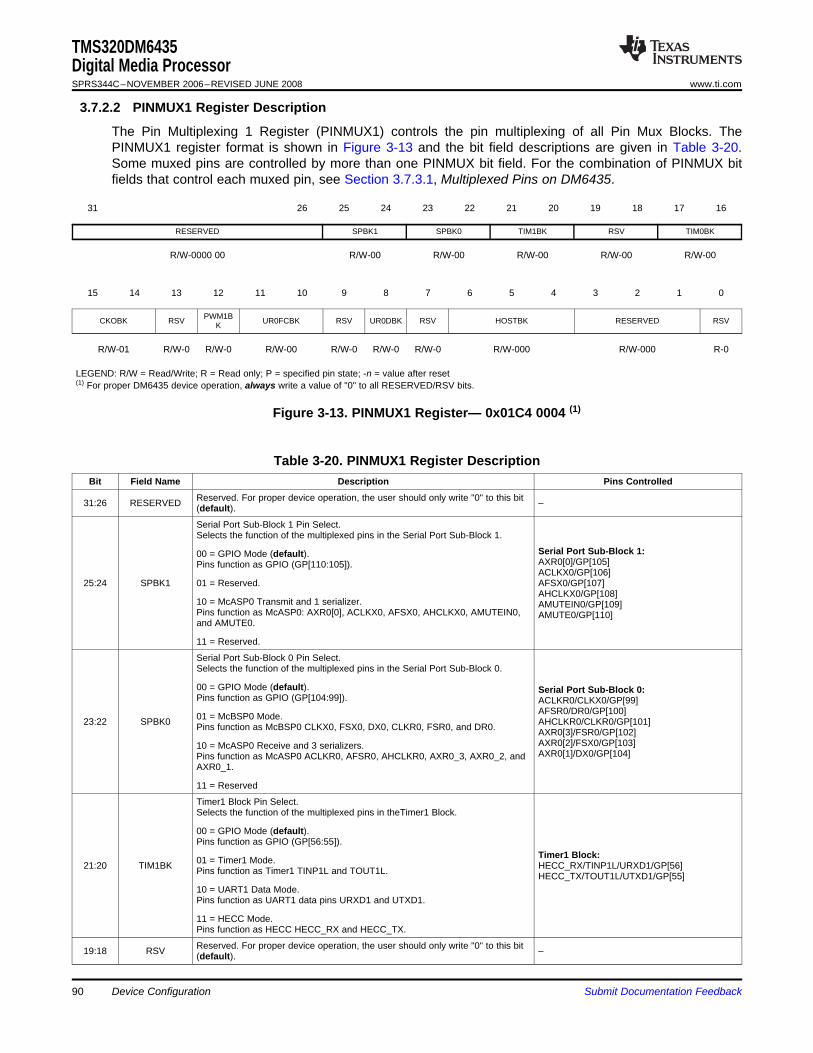
3.7.2.2 PINMUX1 Register Description
TMS320DM6435Digital Media ProcessorSPRS344C–NOVEMBER 2006–REVISED JUNE 2008 www.ti.com
The Pin Multiplexing 1 Register (PINMUX1) controls the pin multiplexing of all Pin Mux Blocks. ThePINMUX1 register format is shown in Figure 3-13 and the bit field descriptions are given in Table 3-20.Some muxed pins are controlled by more than one PINMUX bit field. For the combination of PINMUX bitfields that control each muxed pin, see Section 3.7.3.1, Multiplexed Pins on DM6435.
31 26 25 24 23 22 21 20 19 18 17 16
RESERVED SPBK1 SPBK0 TIM1BK RSV TIM0BK
R/W-0000 00 R/W-00 R/W-00 R/W-00 R/W-00 R/W-00
15 14 13 12 11 10 9 8 7 6 5 4 3 2 1 0
PWM1BCKOBK RSV UR0FCBK RSV UR0DBK RSV HOSTBK RESERVED RSVK
R/W-01 R/W-0 R/W-0 R/W-00 R/W-0 R/W-0 R/W-0 R/W-000 R/W-000 R-0
LEGEND: R/W = Read/Write; R = Read only; P = specified pin state; -n = value after reset(1) For proper DM6435 device operation, always write a value of "0" to all RESERVED/RSV bits.
Figure 3-13. PINMUX1 Register— 0x01C4 0004 (1)
Table 3-20. PINMUX1 Register DescriptionBit Field Name Description Pins Controlled
Reserved. For proper device operation, the user should only write "0" to this bit31:26 RESERVED –(default).
Serial Port Sub-Block 1 Pin Select.Selects the function of the multiplexed pins in the Serial Port Sub-Block 1.
Serial Port Sub-Block 1:00 = GPIO Mode (default).AXR0[0]/GP[105]Pins function as GPIO (GP[110:105]).ACLKX0/GP[106]
25:24 SPBK1 01 = Reserved. AFSX0/GP[107]AHCLKX0/GP[108]
10 = McASP0 Transmit and 1 serializer. AMUTEIN0/GP[109]Pins function as McASP0: AXR0[0], ACLKX0, AFSX0, AHCLKX0, AMUTEIN0, AMUTE0/GP[110]and AMUTE0.
11 = Reserved.
Serial Port Sub-Block 0 Pin Select.Selects the function of the multiplexed pins in the Serial Port Sub-Block 0.
00 = GPIO Mode (default). Serial Port Sub-Block 0:Pins function as GPIO (GP[104:99]). ACLKR0/CLKX0/GP[99]
AFSR0/DR0/GP[100]01 = McBSP0 Mode.23:22 SPBK0 AHCLKR0/CLKR0/GP[101]Pins function as McBSP0 CLKX0, FSX0, DX0, CLKR0, FSR0, and DR0. AXR0[3]/FSR0/GP[102]AXR0[2]/FSX0/GP[103]10 = McASP0 Receive and 3 serializers.AXR0[1]/DX0/GP[104]Pins function as McASP0 ACLKR0, AFSR0, AHCLKR0, AXR0_3, AXR0_2, and
AXR0_1.
11 = Reserved
Timer1 Block Pin Select.Selects the function of the multiplexed pins in theTimer1 Block.
00 = GPIO Mode (default).Pins function as GPIO (GP[56:55]).
Timer1 Block:01 = Timer1 Mode.21:20 TIM1BK HECC_RX/TINP1L/URXD1/GP[56]Pins function as Timer1 TINP1L and TOUT1L. HECC_TX/TOUT1L/UTXD1/GP[55]10 = UART1 Data Mode.Pins function as UART1 data pins URXD1 and UTXD1.
11 = HECC Mode.Pins function as HECC HECC_RX and HECC_TX.
Reserved. For proper device operation, the user should only write "0" to this bit19:18 RSV –(default).
Device Configuration90 Submit Documentation Feedback
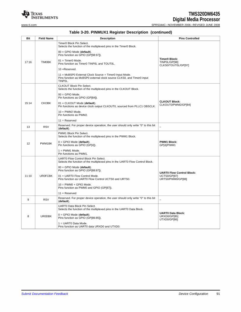
TMS320DM6435Digital Media Processor
www.ti.com SPRS344C–NOVEMBER 2006–REVISED JUNE 2008
Table 3-20. PINMUX1 Register Description (continued)Bit Field Name Description Pins Controlled
Timer0 Block Pin Select.Selects the function of the multiplexed pins in the Timer0 Block.
00 = GPIO Mode (default).Pins function as GPIO (GP[98:97]).
Timer0 Block:01 = Timer0 Mode.17:16 TIM0BK TINP0L/GP[98]Pins function as Timer0 TINP0L and TOUT0L. CLKS0/TOUT0L/GP[97]10 =Reserved.
11 = McBSP0 External Clock Source + Timer0 Input Mode.Pins function as McBSP0 external clock source CLKS0, and Timer0 inputTINP0L.
CLKOUT Block Pin Select.Selects the function of the multiplexed pins in the CLKOUT Block.
00 = GPIO Mode.Pin functions as GPIO (GP[84]).
CLKOUT Block:15:14 CKOBK 01 = CLKOUT Mode (default). CLKOUT0/PWM2/GP[84]Pin functions as device clock output CLKOUT0, sourced from PLLC1 OBSCLK.
10 = PWM2 Mode.Pin functions as PWM2.
11 = Reserved
Reserved. For proper device operation, the user should only write "0" to this bit13 RSV –(default).
PWM1 Block Pin Select.Selects the function of the multiplexed pins in the PWM1 Block.
0 = GPIO Mode (default). PWM1 Block:12 PWM1BK Pin functions as GPIO (GP[4]). GP[4]/PWM1
1 = PWM1 Mode.Pin functions as PWM1.
UART0 Flow Control Block Pin Select.Selects the function of the multiplexed pins in the UART0 Flow Control Block.
00 = GPIO Mode (default).Pins function as GPIO (GP[88:87]).
UART0 Flow Control Block:11:10 UR0FCBK 01 = UART0 Flow Control Mode. UCTS0/GP[87]
Pins function as UART0 Flow Control UCTS0 and URTS0. URTS0/PWM0/GP[88]
10 = PWM0 + GPIO Mode.Pins function as PWM0 and GPIO (GP[87]).
11 = Reserved
Reserved. For proper device operation, the user should only write "0" to this bit9 RSV –(default).
UART0 Data Block Pin Select.Selects the function of the multiplexed pins in the UART0 Data Block.
UART0 Data Block:0 = GPIO Mode (default).8 UR0DBK URXD0/GP[85]Pins function as GPIO (GP[86:85]). UTXD0/GP[86]1 = UART0 Data Mode.Pins function as UART0 data URXD0 and UTXD0.
Submit Documentation Feedback Device Configuration 91
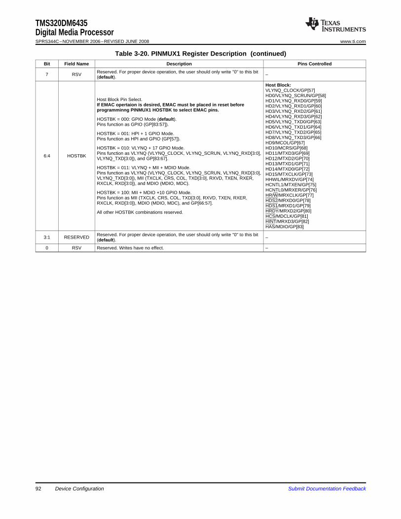
TMS320DM6435Digital Media ProcessorSPRS344C–NOVEMBER 2006–REVISED JUNE 2008 www.ti.com
Table 3-20. PINMUX1 Register Description (continued)Bit Field Name Description Pins Controlled
Reserved. For proper device operation, the user should only write "0" to this bit7 RSV –(default).
Host Block:VLYNQ_CLOCK/GP[57]HD0/VLYNQ_SCRUN/GP[58]
Host Block Pin Select. HD1/VLYNQ_RXD0/GP[59]If EMAC opertaion is desired, EMAC must be placed in reset before HD2/VLYNQ_RXD1/GP[60]programminng PINMUX1 HOSTBK to select EMAC pins. HD3/VLYNQ_RXD2/GP[61]
HD4/VLYNQ_RXD3/GP[62]HOSTBK = 000: GPIO Mode (default). HD5/VLYNQ_TXD0/GP[63]Pins function as GPIO (GP[83:57]). HD6/VLYNQ_TXD1/GP[64]HD7/VLYNQ_TXD2/GP[65]HOSTBK = 001: HPI + 1 GPIO Mode.HD8/VLYNQ_TXD3/GP[66]Pins function as HPI and GPIO (GP[57]).HD9/MCOL/GP[67]
HOSTBK = 010: VLYNQ + 17 GPIO Mode. HD10/MCRS/GP[68]Pins function as VLYNQ (VLYNQ_CLOCK, VLYNQ_SCRUN, VLYNQ_RXD[3:0], HD11/MTXD3/GP[69]6:4 HOSTBK VLYNQ_TXD[3:0]), and GP[83:67]. HD12/MTXD2/GP[70]
HD13/MTXD1/GP[71]HOSTBK = 011: VLYNQ + MII + MDIO Mode. HD14/MTXD0/GP[72]Pins function as VLYNQ (VLYNQ_CLOCK, VLYNQ_SCRUN, VLYNQ_RXD[3:0], HD15/MTXCLK/GP[73]VLYNQ_TXD[3:0]), MII (TXCLK, CRS, COL, TXD[3:0], RXVD, TXEN, RXER, HHWIL/MRXDV/GP[74]RXCLK, RXD[3:0]), and MDIO (MDIO, MDC). HCNTL1/MTXEN/GP[75]
HCNTL0/MRXER/GP[76]HOSTBK = 100: MII + MDIO +10 GPIO Mode. HR/W/MRXCLK/GP[77]Pins function as MII (TXCLK, CRS, COL, TXD[3:0], RXVD, TXEN, RXER, HDS2/MRXD0/GP[78]RXCLK, RXD[3:0]), MDIO (MDIO, MDC), and GP[66:57]. HDS1/MRXD1/GP[79]HRDY/MRXD2/GP[80]All other HOSTBK combinations reserved.HCS/MDCLK/GP[81]HINT/MRXD3/GP[82]HAS/MDIO/GP[83]
Reserved. For proper device operation, the user should only write "0" to this bit3:1 RESERVED –(default).
0 RSV Reserved. Writes have no effect. –
Device Configuration92 Submit Documentation Feedback
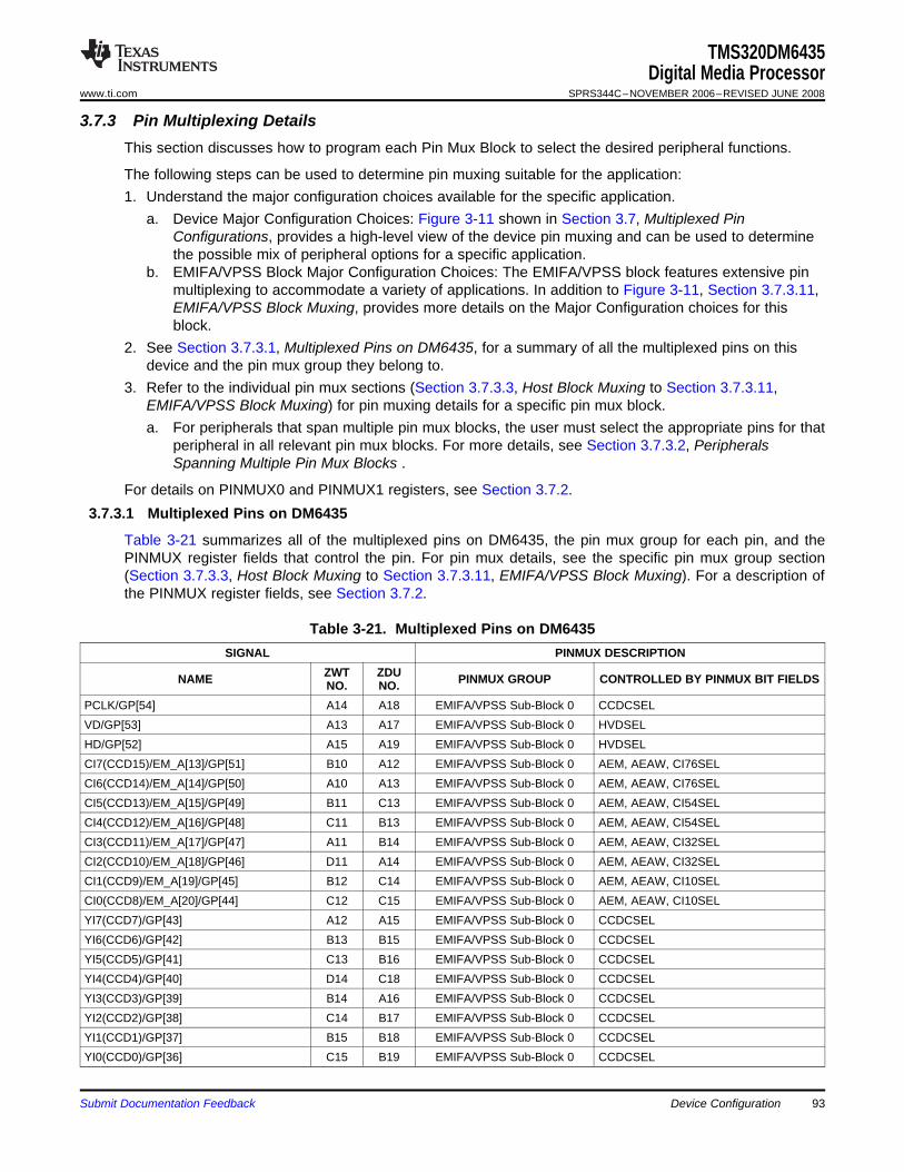
3.7.3 Pin Multiplexing Details
3.7.3.1 Multiplexed Pins on DM6435
TMS320DM6435Digital Media Processor
www.ti.com SPRS344C–NOVEMBER 2006–REVISED JUNE 2008
This section discusses how to program each Pin Mux Block to select the desired peripheral functions.
The following steps can be used to determine pin muxing suitable for the application:1. Understand the major configuration choices available for the specific application.
a. Device Major Configuration Choices: Figure 3-11 shown in Section 3.7, Multiplexed PinConfigurations, provides a high-level view of the device pin muxing and can be used to determinethe possible mix of peripheral options for a specific application.
b. EMIFA/VPSS Block Major Configuration Choices: The EMIFA/VPSS block features extensive pinmultiplexing to accommodate a variety of applications. In addition to Figure 3-11, Section 3.7.3.11,EMIFA/VPSS Block Muxing, provides more details on the Major Configuration choices for thisblock.
2. See Section 3.7.3.1, Multiplexed Pins on DM6435, for a summary of all the multiplexed pins on thisdevice and the pin mux group they belong to.
3. Refer to the individual pin mux sections (Section 3.7.3.3, Host Block Muxing to Section 3.7.3.11,EMIFA/VPSS Block Muxing) for pin muxing details for a specific pin mux block.a. For peripherals that span multiple pin mux blocks, the user must select the appropriate pins for that
peripheral in all relevant pin mux blocks. For more details, see Section 3.7.3.2, PeripheralsSpanning Multiple Pin Mux Blocks .
For details on PINMUX0 and PINMUX1 registers, see Section 3.7.2.
Table 3-21 summarizes all of the multiplexed pins on DM6435, the pin mux group for each pin, and thePINMUX register fields that control the pin. For pin mux details, see the specific pin mux group section(Section 3.7.3.3, Host Block Muxing to Section 3.7.3.11, EMIFA/VPSS Block Muxing). For a description ofthe PINMUX register fields, see Section 3.7.2.
Table 3-21. Multiplexed Pins on DM6435SIGNAL PINMUX DESCRIPTION
ZWT ZDUNAME PINMUX GROUP CONTROLLED BY PINMUX BIT FIELDSNO. NO.PCLK/GP[54] A14 A18 EMIFA/VPSS Sub-Block 0 CCDCSELVD/GP[53] A13 A17 EMIFA/VPSS Sub-Block 0 HVDSELHD/GP[52] A15 A19 EMIFA/VPSS Sub-Block 0 HVDSELCI7(CCD15)/EM_A[13]/GP[51] B10 A12 EMIFA/VPSS Sub-Block 0 AEM, AEAW, CI76SELCI6(CCD14)/EM_A[14]/GP[50] A10 A13 EMIFA/VPSS Sub-Block 0 AEM, AEAW, CI76SELCI5(CCD13)/EM_A[15]/GP[49] B11 C13 EMIFA/VPSS Sub-Block 0 AEM, AEAW, CI54SELCI4(CCD12)/EM_A[16]/GP[48] C11 B13 EMIFA/VPSS Sub-Block 0 AEM, AEAW, CI54SELCI3(CCD11)/EM_A[17]/GP[47] A11 B14 EMIFA/VPSS Sub-Block 0 AEM, AEAW, CI32SELCI2(CCD10)/EM_A[18]/GP[46] D11 A14 EMIFA/VPSS Sub-Block 0 AEM, AEAW, CI32SELCI1(CCD9)/EM_A[19]/GP[45] B12 C14 EMIFA/VPSS Sub-Block 0 AEM, AEAW, CI10SELCI0(CCD8)/EM_A[20]/GP[44] C12 C15 EMIFA/VPSS Sub-Block 0 AEM, AEAW, CI10SELYI7(CCD7)/GP[43] A12 A15 EMIFA/VPSS Sub-Block 0 CCDCSELYI6(CCD6)/GP[42] B13 B15 EMIFA/VPSS Sub-Block 0 CCDCSELYI5(CCD5)/GP[41] C13 B16 EMIFA/VPSS Sub-Block 0 CCDCSELYI4(CCD4)/GP[40] D14 C18 EMIFA/VPSS Sub-Block 0 CCDCSELYI3(CCD3)/GP[39] B14 A16 EMIFA/VPSS Sub-Block 0 CCDCSELYI2(CCD2)/GP[38] C14 B17 EMIFA/VPSS Sub-Block 0 CCDCSELYI1(CCD1)/GP[37] B15 B18 EMIFA/VPSS Sub-Block 0 CCDCSELYI0(CCD0)/GP[36] C15 B19 EMIFA/VPSS Sub-Block 0 CCDCSEL
Submit Documentation Feedback Device Configuration 93
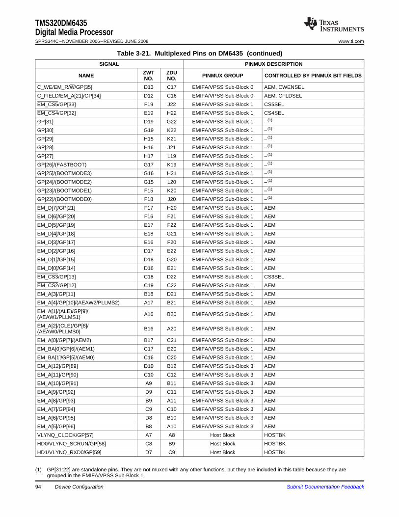
TMS320DM6435Digital Media ProcessorSPRS344C–NOVEMBER 2006–REVISED JUNE 2008 www.ti.com
Table 3-21. Multiplexed Pins on DM6435 (continued)SIGNAL PINMUX DESCRIPTION
ZWT ZDUNAME PINMUX GROUP CONTROLLED BY PINMUX BIT FIELDSNO. NO.C_WE/EM_R/W/GP[35] D13 C17 EMIFA/VPSS Sub-Block 0 AEM, CWENSELC_FIELD/EM_A[21]/GP[34] D12 C16 EMIFA/VPSS Sub-Block 0 AEM, CFLDSELEM_CS5/GP[33] F19 J22 EMIFA/VPSS Sub-Block 1 CS5SELEM_CS4/GP[32] E19 H22 EMIFA/VPSS Sub-Block 1 CS4SELGP[31] D19 G22 EMIFA/VPSS Sub-Block 1 – (1)
GP[30] G19 K22 EMIFA/VPSS Sub-Block 1 – (1)
GP[29] H15 K21 EMIFA/VPSS Sub-Block 1 – (1)
GP[28] H16 J21 EMIFA/VPSS Sub-Block 1 – (1)
GP[27] H17 L19 EMIFA/VPSS Sub-Block 1 – (1)
GP[26]/(FASTBOOT) G17 K19 EMIFA/VPSS Sub-Block 1 – (1)
GP[25]/(BOOTMODE3) G16 H21 EMIFA/VPSS Sub-Block 1 – (1)
GP[24]/(BOOTMODE2) G15 L20 EMIFA/VPSS Sub-Block 1 – (1)
GP[23]/(BOOTMODE1) F15 K20 EMIFA/VPSS Sub-Block 1 – (1)
GP[22]/(BOOTMODE0) F18 J20 EMIFA/VPSS Sub-Block 1 – (1)
EM_D[7]/GP[21] F17 H20 EMIFA/VPSS Sub-Block 1 AEMEM_D[6]/GP[20] F16 F21 EMIFA/VPSS Sub-Block 1 AEMEM_D[5]/GP[19] E17 F22 EMIFA/VPSS Sub-Block 1 AEMEM_D[4]/GP[18] E18 G21 EMIFA/VPSS Sub-Block 1 AEMEM_D[3]/GP[17] E16 F20 EMIFA/VPSS Sub-Block 1 AEMEM_D[2]/GP[16] D17 E22 EMIFA/VPSS Sub-Block 1 AEMEM_D[1]/GP[15] D18 G20 EMIFA/VPSS Sub-Block 1 AEMEM_D[0]/GP[14] D16 E21 EMIFA/VPSS Sub-Block 1 AEMEM_CS3/GP[13] C18 D22 EMIFA/VPSS Sub-Block 1 CS3SELEM_CS2/GP[12] C19 C22 EMIFA/VPSS Sub-Block 1 AEMEM_A[3]/GP[11] B18 D21 EMIFA/VPSS Sub-Block 1 AEMEM_A[4]/GP[10]/(AEAW2/PLLMS2) A17 B21 EMIFA/VPSS Sub-Block 1 AEMEM_A[1]/(ALE)/GP[9]/ A16 B20 EMIFA/VPSS Sub-Block 1 AEM(AEAW1/PLLMS1)EM_A[2]/(CLE)/GP[8]/ B16 A20 EMIFA/VPSS Sub-Block 1 AEM(AEAW0/PLLMS0)EM_A[0]/GP[7]/(AEM2) B17 C21 EMIFA/VPSS Sub-Block 1 AEMEM_BA[0]/GP[6]/(AEM1) C17 E20 EMIFA/VPSS Sub-Block 1 AEMEM_BA[1]/GP[5]/(AEM0) C16 C20 EMIFA/VPSS Sub-Block 1 AEMEM_A[12]/GP[89] D10 B12 EMIFA/VPSS Sub-Block 3 AEMEM_A[11]/GP[90] C10 C12 EMIFA/VPSS Sub-Block 3 AEMEM_A[10]/GP[91] A9 B11 EMIFA/VPSS Sub-Block 3 AEMEM_A[9]/GP[92] D9 C11 EMIFA/VPSS Sub-Block 3 AEMEM_A[8]/GP[93] B9 A11 EMIFA/VPSS Sub-Block 3 AEMEM_A[7]/GP[94] C9 C10 EMIFA/VPSS Sub-Block 3 AEMEM_A[6]/GP[95] D8 B10 EMIFA/VPSS Sub-Block 3 AEMEM_A[5]/GP[96] B8 A10 EMIFA/VPSS Sub-Block 3 AEMVLYNQ_CLOCK/GP[57] A7 A8 Host Block HOSTBKHD0/VLYNQ_SCRUN/GP[58] C8 B9 Host Block HOSTBKHD1/VLYNQ_RXD0/GP[59] D7 C9 Host Block HOSTBK
(1) GP[31:22] are standalone pins. They are not muxed with any other functions, but they are included in this table because they aregrouped in the EMIFA/VPSS Sub-Block 1.
Device Configuration94 Submit Documentation Feedback
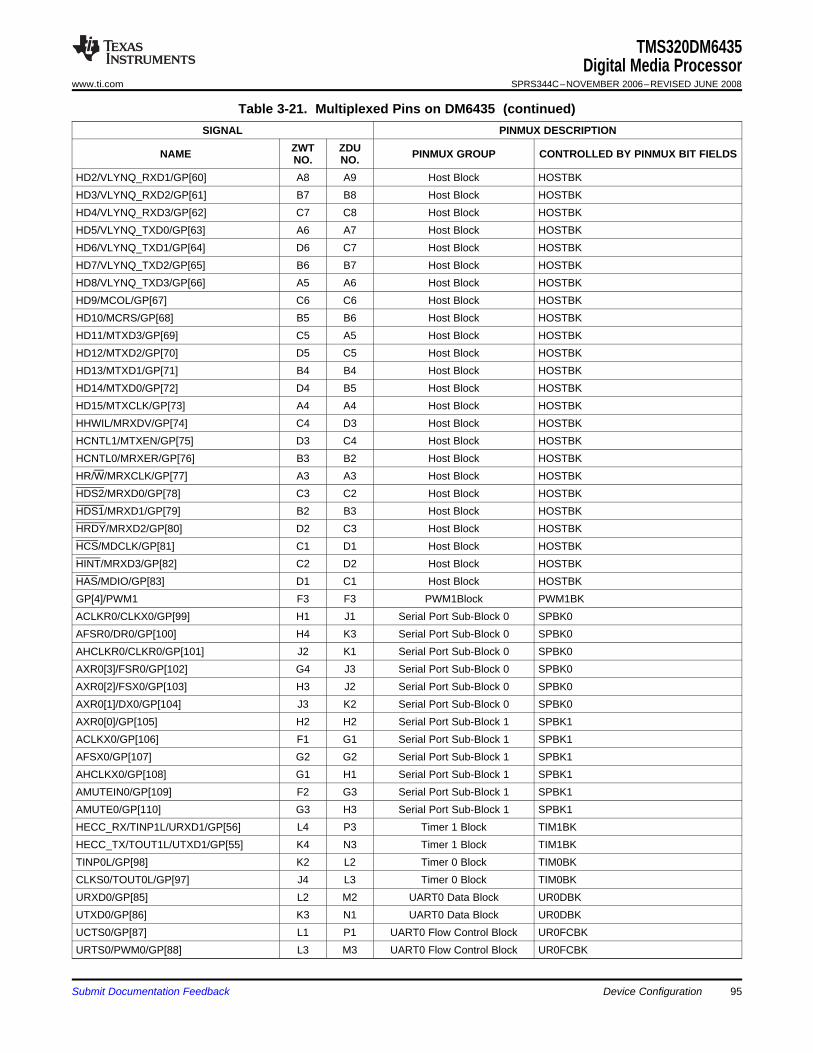
TMS320DM6435Digital Media Processor
www.ti.com SPRS344C–NOVEMBER 2006–REVISED JUNE 2008
Table 3-21. Multiplexed Pins on DM6435 (continued)SIGNAL PINMUX DESCRIPTION
ZWT ZDUNAME PINMUX GROUP CONTROLLED BY PINMUX BIT FIELDSNO. NO.HD2/VLYNQ_RXD1/GP[60] A8 A9 Host Block HOSTBKHD3/VLYNQ_RXD2/GP[61] B7 B8 Host Block HOSTBKHD4/VLYNQ_RXD3/GP[62] C7 C8 Host Block HOSTBKHD5/VLYNQ_TXD0/GP[63] A6 A7 Host Block HOSTBKHD6/VLYNQ_TXD1/GP[64] D6 C7 Host Block HOSTBKHD7/VLYNQ_TXD2/GP[65] B6 B7 Host Block HOSTBKHD8/VLYNQ_TXD3/GP[66] A5 A6 Host Block HOSTBKHD9/MCOL/GP[67] C6 C6 Host Block HOSTBKHD10/MCRS/GP[68] B5 B6 Host Block HOSTBKHD11/MTXD3/GP[69] C5 A5 Host Block HOSTBKHD12/MTXD2/GP[70] D5 C5 Host Block HOSTBKHD13/MTXD1/GP[71] B4 B4 Host Block HOSTBKHD14/MTXD0/GP[72] D4 B5 Host Block HOSTBKHD15/MTXCLK/GP[73] A4 A4 Host Block HOSTBKHHWIL/MRXDV/GP[74] C4 D3 Host Block HOSTBKHCNTL1/MTXEN/GP[75] D3 C4 Host Block HOSTBKHCNTL0/MRXER/GP[76] B3 B2 Host Block HOSTBKHR/W/MRXCLK/GP[77] A3 A3 Host Block HOSTBKHDS2/MRXD0/GP[78] C3 C2 Host Block HOSTBKHDS1/MRXD1/GP[79] B2 B3 Host Block HOSTBKHRDY/MRXD2/GP[80] D2 C3 Host Block HOSTBKHCS/MDCLK/GP[81] C1 D1 Host Block HOSTBKHINT/MRXD3/GP[82] C2 D2 Host Block HOSTBKHAS/MDIO/GP[83] D1 C1 Host Block HOSTBKGP[4]/PWM1 F3 F3 PWM1Block PWM1BKACLKR0/CLKX0/GP[99] H1 J1 Serial Port Sub-Block 0 SPBK0AFSR0/DR0/GP[100] H4 K3 Serial Port Sub-Block 0 SPBK0AHCLKR0/CLKR0/GP[101] J2 K1 Serial Port Sub-Block 0 SPBK0AXR0[3]/FSR0/GP[102] G4 J3 Serial Port Sub-Block 0 SPBK0AXR0[2]/FSX0/GP[103] H3 J2 Serial Port Sub-Block 0 SPBK0AXR0[1]/DX0/GP[104] J3 K2 Serial Port Sub-Block 0 SPBK0AXR0[0]/GP[105] H2 H2 Serial Port Sub-Block 1 SPBK1ACLKX0/GP[106] F1 G1 Serial Port Sub-Block 1 SPBK1AFSX0/GP[107] G2 G2 Serial Port Sub-Block 1 SPBK1AHCLKX0/GP[108] G1 H1 Serial Port Sub-Block 1 SPBK1AMUTEIN0/GP[109] F2 G3 Serial Port Sub-Block 1 SPBK1AMUTE0/GP[110] G3 H3 Serial Port Sub-Block 1 SPBK1HECC_RX/TINP1L/URXD1/GP[56] L4 P3 Timer 1 Block TIM1BKHECC_TX/TOUT1L/UTXD1/GP[55] K4 N3 Timer 1 Block TIM1BKTINP0L/GP[98] K2 L2 Timer 0 Block TIM0BKCLKS0/TOUT0L/GP[97] J4 L3 Timer 0 Block TIM0BKURXD0/GP[85] L2 M2 UART0 Data Block UR0DBKUTXD0/GP[86] K3 N1 UART0 Data Block UR0DBKUCTS0/GP[87] L1 P1 UART0 Flow Control Block UR0FCBKURTS0/PWM0/GP[88] L3 M3 UART0 Flow Control Block UR0FCBK
Submit Documentation Feedback Device Configuration 95
3.7.3.2 Peripherals Spanning Multiple Pin Mux Blocks
TMS320DM6435Digital Media ProcessorSPRS344C–NOVEMBER 2006–REVISED JUNE 2008 www.ti.com
Table 3-21. Multiplexed Pins on DM6435 (continued)SIGNAL PINMUX DESCRIPTION
ZWT ZDUNAME PINMUX GROUP CONTROLLED BY PINMUX BIT FIELDSNO. NO.CLKOUT0/PWM2/GP[84] M1 R1 CLKOUT Block CKOBK
Note: PINMUX group EMIFA/VPSS Sub-Block 2 is not shown in the above table because there is noactual pin multiplexing in that block. But this block is still considered a "pin mux block" because it containssome of the pins necessary for EMIFA. The pins in this block are as follows:• EMIFA/VPSS Sub-Block 2
– EM_WAIT/(RDY/BSY)– EM_OE– EM_WE
Some peripherals span multiple Pin Mux Blocks. To use these peripherals, they must be selected in all ofthe relevant Pin Mux Blocks. The following is the list of peripherals that span multiple Pin Mux Blocks:• McBSP0: Six McBSP0 pins are located in the Serial Port Sub-Block 0, but the CLKS0 pin is muxed in
the Timer0 Block. To select McBSP0 pins, program PINMUX registers as follows:– Serial Port Sub-Block 0: SPBK0 = 01– Timer0 Block: If CLKS0 pin is desired, program TIM0BK = 10 or 11.
• UART0: The two UART0 data pins are located in the UART0 Data Block, but the two UART0 flowcontrol pins are located in the UART0 Flow Control Block. To select UART0, program PINMUXregisters as follows:– UART0 Data Block: UR0BK = 1– UART0 Flow Control Block: If flow control pins are desired, program UR0FCBK = 01.
Device Configuration96 Submit Documentation Feedback
3.7.3.3 Host Block Muxing
TMS320DM6435Digital Media Processor
www.ti.com SPRS344C–NOVEMBER 2006–REVISED JUNE 2008
This block of 27 pins consists of HPI, VLYNQ, EMAC, MDIO, and GPIO muxed pins. The followingregister field selects the pin functions in the Host Block:• PINMUX1.HOSTBK
Table 3-22 summarizes the 27 pins in the Host Block, the multiplexed function on each pin, and thePINMUX configurations to select the corresponding function.
Submit Documentation Feedback Device Configuration 97
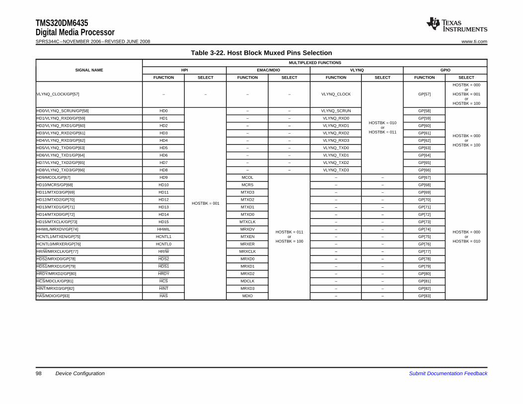
TMS320DM6435Digital Media ProcessorSPRS344C–NOVEMBER 2006–REVISED JUNE 2008 www.ti.com
Table 3-22. Host Block Muxed Pins SelectionMULTIPLEXED FUNCTIONS
SIGNAL NAME HPI EMAC/MDIO VLYNQ GPIO
FUNCTION SELECT FUNCTION SELECT FUNCTION SELECT FUNCTION SELECT
HOSTBK = 000or
VLYNQ_CLOCK/GP[57] – – – – VLYNQ_CLOCK GP[57] HOSTBK = 001or
HOSTBK = 100
HD0/VLYNQ_SCRUN/GP[58] HD0 – – VLYNQ_SCRUN GP[58]
HD1/VLYNQ_RXD0/GP[59] HD1 – – VLYNQ_RXD0 GP[59]HOSTBK = 010
HD2/VLYNQ_RXD1/GP[60] HD2 – – VLYNQ_RXD1 GP[60]orHOSTBK = 011HD3/VLYNQ_RXD2/GP[61] HD3 – – VLYNQ_RXD2 GP[61]
HOSTBK = 000HD4/VLYNQ_RXD3/GP[62] HD4 – – VLYNQ_RXD3 GP[62] or
HOSTBK = 100HD5/VLYNQ_TXD0/GP[63] HD5 – – VLYNQ_TXD0 GP[63]
HD6/VLYNQ_TXD1/GP[64] HD6 – – VLYNQ_TXD1 GP[64]
HD7/VLYNQ_TXD2/GP[65] HD7 – – VLYNQ_TXD2 GP[65]
HD8/VLYNQ_TXD3/GP[66] HD8 – – VLYNQ_TXD3 GP[66]
HD9/MCOL/GP[67] HD9 MCOL – – GP[67]
HD10/MCRS/GP[68] HD10 MCRS – – GP[68]
HD11/MTXD3/GP[69] HD11 MTXD3 – – GP[69]
HD12/MTXD2/GP[70] HD12 MTXD2 – – GP[70]HOSTBK = 001
HD13/MTXD1/GP[71] HD13 MTXD1 – – GP[71]
HD14/MTXD0/GP[72] HD14 MTXD0 – – GP[72]
HD15/MTXCLK/GP[73] HD15 MTXCLK – – GP[73]
HHWIL/MRXDV/GP[74] HHWIL MRXDV – – GP[74]HOSTBK = 011 HOSTBK = 000
HCNTL1/MTXEN/GP[75] HCNTL1 MTXEN or – – GP[75] orHOSTBK = 100 HOSTBK = 010
HCNTL0/MRXER/GP[76] HCNTL0 MRXER – – GP[76]
HR/W/MRXCLK/GP[77] HR/W MRXCLK – – GP[77]
HDS2/MRXD0/GP[78] HDS2 MRXD0 – – GP[78]
HDS1/MRXD1/GP[79] HDS1 MRXD1 – – GP[79]
HRDY/MRXD2/GP[80] HRDY MRXD2 – – GP[80]
HCS/MDCLK/GP[81] HCS MDCLK – – GP[81]
HINT/MRXD3/GP[82] HINT MRXD3 – – GP[82]
HAS/MDIO/GP[83] HAS MDIO – – GP[83]
98 Device Configuration Submit Documentation Feedback
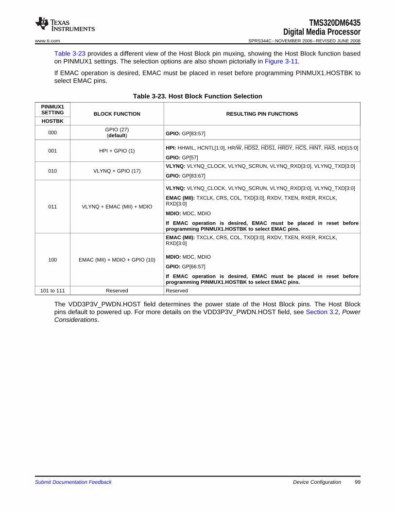
TMS320DM6435Digital Media Processor
www.ti.com SPRS344C–NOVEMBER 2006–REVISED JUNE 2008
Table 3-23 provides a different view of the Host Block pin muxing, showing the Host Block function basedon PINMUX1 settings. The selection options are also shown pictorially in Figure 3-11.
If EMAC operation is desired, EMAC must be placed in reset before programming PINMUX1.HOSTBK toselect EMAC pins.
Table 3-23. Host Block Function SelectionPINMUX1SETTING BLOCK FUNCTION RESULTING PIN FUNCTIONSHOSTBK
GPIO (27)000 GPIO: GP[83:57](default)
HPI: HHWIL, HCNTL[1:0], HR/W, HDS2, HDS1, HRDY, HCS, HINT, HAS, HD[15:0]001 HPI + GPIO (1)GPIO: GP[57]VLYNQ: VLYNQ_CLOCK, VLYNQ_SCRUN, VLYNQ_RXD[3:0], VLYNQ_TXD[3:0]
010 VLYNQ + GPIO (17)GPIO: GP[83:67]
VLYNQ: VLYNQ_CLOCK, VLYNQ_SCRUN, VLYNQ_RXD[3:0], VLYNQ_TXD[3:0]
EMAC (MII): TXCLK, CRS, COL, TXD[3:0], RXDV, TXEN, RXER, RXCLK,RXD[3:0]011 VLYNQ + EMAC (MII) + MDIOMDIO: MDC, MDIO
If EMAC operation is desired, EMAC must be placed in reset beforeprogramming PINMUX1.HOSTBK to select EMAC pins.EMAC (MII): TXCLK, CRS, COL, TXD[3:0], RXDV, TXEN, RXER, RXCLK,RXD[3:0]
MDIO: MDC, MDIO100 EMAC (MII) + MDIO + GPIO (10)GPIO: GP[66:57]
If EMAC operation is desired, EMAC must be placed in reset beforeprogramming PINMUX1.HOSTBK to select EMAC pins.
101 to 111 Reserved Reserved
The VDD3P3V_PWDN.HOST field determines the power state of the Host Block pins. The Host Blockpins default to powered up. For more details on the VDD3P3V_PWDN.HOST field, see Section 3.2, PowerConsiderations.
Submit Documentation Feedback Device Configuration 99
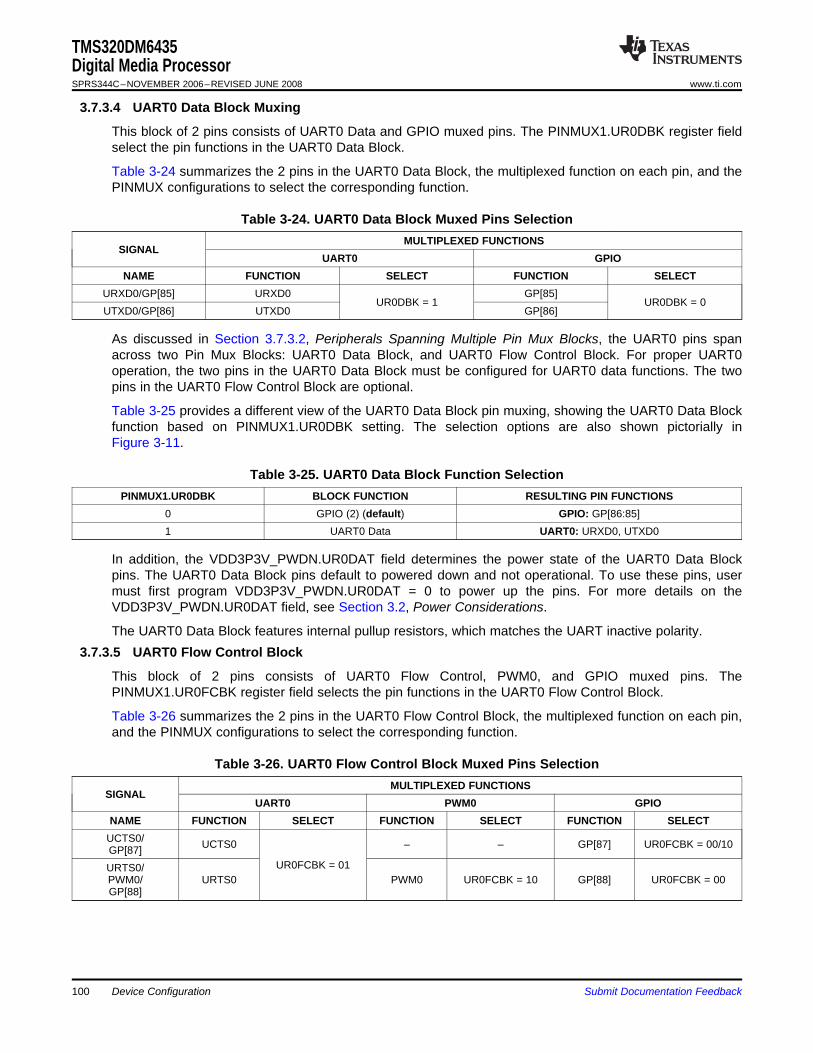
3.7.3.4 UART0 Data Block Muxing
3.7.3.5 UART0 Flow Control Block
TMS320DM6435Digital Media ProcessorSPRS344C–NOVEMBER 2006–REVISED JUNE 2008 www.ti.com
This block of 2 pins consists of UART0 Data and GPIO muxed pins. The PINMUX1.UR0DBK register fieldselect the pin functions in the UART0 Data Block.
Table 3-24 summarizes the 2 pins in the UART0 Data Block, the multiplexed function on each pin, and thePINMUX configurations to select the corresponding function.
Table 3-24. UART0 Data Block Muxed Pins SelectionMULTIPLEXED FUNCTIONS
SIGNALUART0 GPIO
NAME FUNCTION SELECT FUNCTION SELECTURXD0/GP[85] URXD0 GP[85]
UR0DBK = 1 UR0DBK = 0UTXD0/GP[86] UTXD0 GP[86]
As discussed in Section 3.7.3.2, Peripherals Spanning Multiple Pin Mux Blocks, the UART0 pins spanacross two Pin Mux Blocks: UART0 Data Block, and UART0 Flow Control Block. For proper UART0operation, the two pins in the UART0 Data Block must be configured for UART0 data functions. The twopins in the UART0 Flow Control Block are optional.
Table 3-25 provides a different view of the UART0 Data Block pin muxing, showing the UART0 Data Blockfunction based on PINMUX1.UR0DBK setting. The selection options are also shown pictorially inFigure 3-11.
Table 3-25. UART0 Data Block Function SelectionPINMUX1.UR0DBK BLOCK FUNCTION RESULTING PIN FUNCTIONS
0 GPIO (2) (default) GPIO: GP[86:85]1 UART0 Data UART0: URXD0, UTXD0
In addition, the VDD3P3V_PWDN.UR0DAT field determines the power state of the UART0 Data Blockpins. The UART0 Data Block pins default to powered down and not operational. To use these pins, usermust first program VDD3P3V_PWDN.UR0DAT = 0 to power up the pins. For more details on theVDD3P3V_PWDN.UR0DAT field, see Section 3.2, Power Considerations.
The UART0 Data Block features internal pullup resistors, which matches the UART inactive polarity.
This block of 2 pins consists of UART0 Flow Control, PWM0, and GPIO muxed pins. ThePINMUX1.UR0FCBK register field selects the pin functions in the UART0 Flow Control Block.
Table 3-26 summarizes the 2 pins in the UART0 Flow Control Block, the multiplexed function on each pin,and the PINMUX configurations to select the corresponding function.
Table 3-26. UART0 Flow Control Block Muxed Pins SelectionMULTIPLEXED FUNCTIONS
SIGNALUART0 PWM0 GPIO
NAME FUNCTION SELECT FUNCTION SELECT FUNCTION SELECTUCTS0/ UCTS0 – – GP[87] UR0FCBK = 00/10GP[87]
UR0FCBK = 01URTS0/PWM0/ URTS0 PWM0 UR0FCBK = 10 GP[88] UR0FCBK = 00GP[88]
Device Configuration100 Submit Documentation Feedback
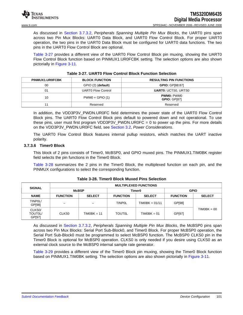
3.7.3.6 Timer0 Block
TMS320DM6435Digital Media Processor
www.ti.com SPRS344C–NOVEMBER 2006–REVISED JUNE 2008
As discussed in Section 3.7.3.2, Peripherals Spanning Multiple Pin Mux Blocks, the UART0 pins spanacross two Pin Mux Blocks: UART0 Data Block, and UART0 Flow Control Block. For proper UART0operation, the two pins in the UART0 Data Block must be configured for UART0 data functions. The twopins in the UART0 Flow Control Block are optional.
Table 3-27 provides a different view of the UART0 Flow Control Block pin muxing, showing the UART0Flow Control Block function based on PINMUX1.UR0FCBK setting. The selection options are also shownpictorially in Figure 3-11.
Table 3-27. UART0 Flow Control Block Function SelectionPINMUX1.UR0FCBK BLOCK FUNCTION RESULTING PIN FUNCTIONS
00 GPIO (2) (default) GPIO: GP[88:87]01 UART0 Flow Control UART0: UCTS0, URTS0
PWM0: PWM010 PWM0 + GPIO (1) GPIO: GP[87]11 Reserved Reserved
In addition, the VDD3P3V_PWDN.UR0FC field determines the power state of the UART0 Flow ControlBlock pins. The UART0 Flow Control Block pins default to powered down and not operational. To usethese pins, user must first program VDD3P3V_PWDN.UR0FC = 0 to power up the pins. For more detailson the VDD3P3V_PWDN.UR0FC field, see Section 3.2, Power Considerations.
The UART0 Flow Control Block features internal pullup resistors, which matches the UART inactivepolarity.
This block of 2 pins consists of Timer0, McBSP0, and GPIO muxed pins. The PINMUX1.TIM0BK registerfield selects the pin functions in the Timer0 Block.
Table 3-28 summarizes the 2 pins in the Timer0 Block, the multiplexed function on each pin, and thePINMUX configurations to select the corresponding function.
Table 3-28. Timer0 Block Muxed Pins SelectionMULTIPLEXED FUNCTIONS
SIGNALMcBSP Timer0 GPIO
NAME FUNCTION SELECT FUNCTION SELECT FUNCTION SELECTTINP0L/ – – TINP0L TIM0BK = 01/11 GP[98]GP[98]
TIM0BK = 00CLKS0/TOUT0L/ CLKS0 TIM0BK = 11 TOUT0L TIM0BK = 01 GP[97]GP[97]
As discussed in Section 3.7.3.2, Peripherals Spanning Multiple Pin Mux Blocks, the McBSP0 pins spanacross two Pin Mux Blocks: Serial Port Sub-Block0, and Timer0 Block. For proper McBSP0 operation, theSerial Port Sub-Block0 must be programmed to select McBSP0 function. The McBSP0 CLKS0 pin in theTimer0 Block is optional for McBSP0 operation. CLKS0 is only needed if you desire using CLKS0 as anexternal clock source to the McBSP0 internal sample rate generator.
Table 3-29 provides a different view of the Timer0 Block pin muxing, showing the Timer0 Block functionbased on PINMUX1.TIM0BK setting. The selection options are also shown pictorially in Figure 3-11.
Submit Documentation Feedback Device Configuration 101
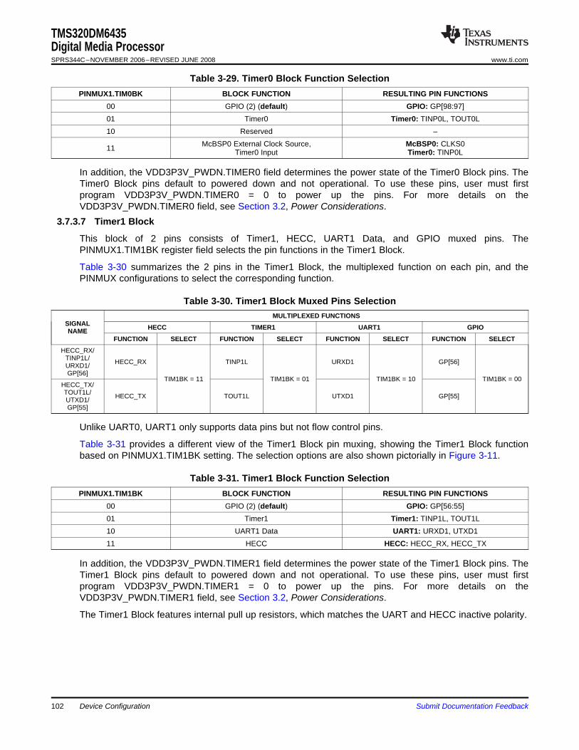
3.7.3.7 Timer1 Block
TMS320DM6435Digital Media ProcessorSPRS344C–NOVEMBER 2006–REVISED JUNE 2008 www.ti.com
Table 3-29. Timer0 Block Function SelectionPINMUX1.TIM0BK BLOCK FUNCTION RESULTING PIN FUNCTIONS
00 GPIO (2) (default) GPIO: GP[98:97]01 Timer0 Timer0: TINP0L, TOUT0L10 Reserved –
McBSP0 External Clock Source, McBSP0: CLKS011 Timer0 Input Timer0: TINP0L
In addition, the VDD3P3V_PWDN.TIMER0 field determines the power state of the Timer0 Block pins. TheTimer0 Block pins default to powered down and not operational. To use these pins, user must firstprogram VDD3P3V_PWDN.TIMER0 = 0 to power up the pins. For more details on theVDD3P3V_PWDN.TIMER0 field, see Section 3.2, Power Considerations.
This block of 2 pins consists of Timer1, HECC, UART1 Data, and GPIO muxed pins. ThePINMUX1.TIM1BK register field selects the pin functions in the Timer1 Block.
Table 3-30 summarizes the 2 pins in the Timer1 Block, the multiplexed function on each pin, and thePINMUX configurations to select the corresponding function.
Table 3-30. Timer1 Block Muxed Pins SelectionMULTIPLEXED FUNCTIONS
SIGNAL HECC TIMER1 UART1 GPIONAMEFUNCTION SELECT FUNCTION SELECT FUNCTION SELECT FUNCTION SELECT
HECC_RX/TINP1L/ HECC_RX TINP1L URXD1 GP[56]URXD1/GP[56]
TIM1BK = 11 TIM1BK = 01 TIM1BK = 10 TIM1BK = 00HECC_TX/TOUT1L/ HECC_TX TOUT1L UTXD1 GP[55]UTXD1/GP[55]
Unlike UART0, UART1 only supports data pins but not flow control pins.
Table 3-31 provides a different view of the Timer1 Block pin muxing, showing the Timer1 Block functionbased on PINMUX1.TIM1BK setting. The selection options are also shown pictorially in Figure 3-11.
Table 3-31. Timer1 Block Function SelectionPINMUX1.TIM1BK BLOCK FUNCTION RESULTING PIN FUNCTIONS
00 GPIO (2) (default) GPIO: GP[56:55]01 Timer1 Timer1: TINP1L, TOUT1L10 UART1 Data UART1: URXD1, UTXD111 HECC HECC: HECC_RX, HECC_TX
In addition, the VDD3P3V_PWDN.TIMER1 field determines the power state of the Timer1 Block pins. TheTimer1 Block pins default to powered down and not operational. To use these pins, user must firstprogram VDD3P3V_PWDN.TIMER1 = 0 to power up the pins. For more details on theVDD3P3V_PWDN.TIMER1 field, see Section 3.2, Power Considerations.
The Timer1 Block features internal pull up resistors, which matches the UART and HECC inactive polarity.
Device Configuration102 Submit Documentation Feedback
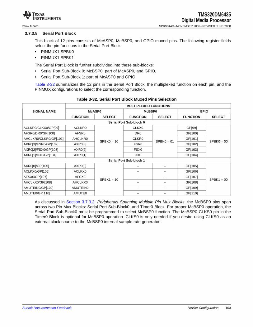
3.7.3.8 Serial Port Block
TMS320DM6435Digital Media Processor
www.ti.com SPRS344C–NOVEMBER 2006–REVISED JUNE 2008
This block of 12 pins consists of McASP0, McBSP0, and GPIO muxed pins. The following register fieldsselect the pin functions in the Serial Port Block:• PINMUX1.SPBK0• PINMUX1.SPBK1
The Serial Port Block is further subdivided into these sub-blocks:• Serial Port Sub-Block 0: McBSP0, part of McASP0, and GPIO.• Serial Port Sub-Block 1: part of McASP0 and GPIO.
Table 3-32 summarizes the 12 pins in the Serial Port Block, the multiplexed function on each pin, and thePINMUX configurations to select the corresponding function.
Table 3-32. Serial Port Block Muxed Pins SelectionMULTIPLEXED FUNCTIONS
SIGNAL NAME McASP0 McBSP0 GPIOFUNCTION SELECT FUNCTION SELECT FUNCTION SELECT
Serial Port Sub-block 0ACLKR0/CLKX0/GP[99] ACLKR0 CLKX0 GP[99]AFSR0/DR0/GP[100] AFSR0 DR0 GP[100]AHCLKR0/CLKR0/GP[101] AHCLKR0 CLKR0 GP[101]
SPBK0 = 10 SPBK0 = 01 SPBK0 = 00AXR0[3]/FSR0/GP[102] AXR0[3] FSR0 GP[102]AXR0[2]/FSX0/GP[103] AXR0[2] FSX0 GP[103]AXR0[1]/DX0/GP[104] AXR0[1] DX0 GP[104]
Serial Port Sub-block 1AXR0[0]/GP[105] AXR0[0] – – GP[105]ACLKX0/GP[106] ACLKX0 – – GP[106]AFSX0/GP[107] AFSX0 – – GP[107]
SPBK1 = 10 SPBK1 = 00AHCLKX0/GP[108] AHCLKX0 – – GP[108]AMUTEIN0/GP[109] AMUTEIN0 – – GP[109]AMUTE0/GP[110] AMUTE0 – – GP[110]
As discussed in Section 3.7.3.2, Peripherals Spanning Multiple Pin Mux Blocks, the McBSP0 pins spanacross two Pin Mux Blocks: Serial Port Sub-Block0, and Timer0 Block. For proper McBSP0 operation, theSerial Port Sub-Block0 must be programmed to select McBSP0 function. The McBSP0 CLKS0 pin in theTimer0 Block is optional for McBSP0 operation. CLKS0 is only needed if you desire using CLKS0 as anexternal clock source to the McBSP0 internal sample rate generator.
Submit Documentation Feedback Device Configuration 103
TMS320DM6435Digital Media ProcessorSPRS344C–NOVEMBER 2006–REVISED JUNE 2008 www.ti.com
Table 3-33 and Table 3-34 provide a different view of the Serial Port Block. Table 3-33 shows the SerialPort Sub-Block 0 function based on PINMUX1.SPBK0 setting. Table 3-34 shows the Serial Port Sub-Block1 function based on PINMUX1.SPBK1 setting. These selection options are also shown pictorially inFigure 3-11.
Table 3-33. Serial Port Sub-Block 0 Function SelectionPINMUX1.SPBK0 BLOCK FUNCTION RESULTING PIN FUNCTIONS
00 GPIO (6) (default) GPIO: GP[104:99]01 McBSP0 McBSP0: CLKX0, FSX0, DX0, CLKR0, FSR0, DR0
McASP0: ACLKR0, AFSR0, AHCLKR0, AXR0[3],10 McASP0 Receive, 3 Serializers AXR0[2], AXR0[1]11 Reserved Reserved
Table 3-34. Serial Port Sub-Block 1 Function SelectionPINMUX1.SPBK1 BLOCK FUNCTION RESULTING PIN FUNCTIONS
00 GPIO (6) (default) GPIO: GP[110:105]01 Reserved –
McASP0 Transmit with 1 Serializer and McASP0: AXR0[0], ACLKX0, AFSX0, AHCLKX0,10 Mute Control AMUTEIN0 (1), AMUTE011 Reserved –
(1) The input from the AMUTEIN0/GP[109] pin is connected to both the McASP0 and GPIO.
In addition, the VDD3P3V_PWDN.SP field determines the power state of the Serial Port Block pins. TheSerial Port Block pins default to powered down and not operational. To use these pins, user must firstprogram VDD3P3V_PWDN.SP = 0 to power up the pins. For more details on the VDD3P3V_PWDN.SPfield, see Section 3.2, Power Considerations.
To facilitate McASP0 operation, the input from the AMUTEIN0/GP[109] pin is connected to both theMcASP0 and the GPIO module. Therefore when an external mute event occurs, in addition to notifying theMcASP0, it can also cause an interrupt through the GPIO module.
Device Configuration104 Submit Documentation Feedback
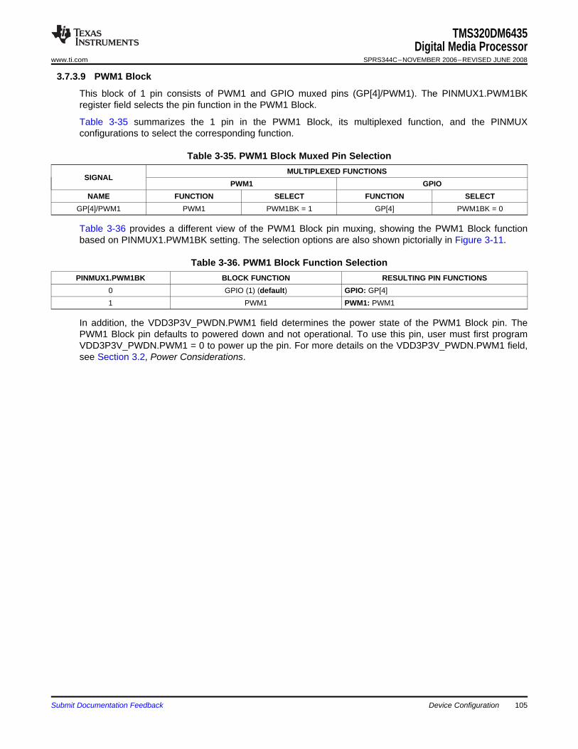
3.7.3.9 PWM1 Block
TMS320DM6435Digital Media Processor
www.ti.com SPRS344C–NOVEMBER 2006–REVISED JUNE 2008
This block of 1 pin consists of PWM1 and GPIO muxed pins (GP[4]/PWM1). The PINMUX1.PWM1BKregister field selects the pin function in the PWM1 Block.
Table 3-35 summarizes the 1 pin in the PWM1 Block, its multiplexed function, and the PINMUXconfigurations to select the corresponding function.
Table 3-35. PWM1 Block Muxed Pin SelectionMULTIPLEXED FUNCTIONS
SIGNALPWM1 GPIO
NAME FUNCTION SELECT FUNCTION SELECTGP[4]/PWM1 PWM1 PWM1BK = 1 GP[4] PWM1BK = 0
Table 3-36 provides a different view of the PWM1 Block pin muxing, showing the PWM1 Block functionbased on PINMUX1.PWM1BK setting. The selection options are also shown pictorially in Figure 3-11.
Table 3-36. PWM1 Block Function SelectionPINMUX1.PWM1BK BLOCK FUNCTION RESULTING PIN FUNCTIONS
0 GPIO (1) (default) GPIO: GP[4]1 PWM1 PWM1: PWM1
In addition, the VDD3P3V_PWDN.PWM1 field determines the power state of the PWM1 Block pin. ThePWM1 Block pin defaults to powered down and not operational. To use this pin, user must first programVDD3P3V_PWDN.PWM1 = 0 to power up the pin. For more details on the VDD3P3V_PWDN.PWM1 field,see Section 3.2, Power Considerations.
Submit Documentation Feedback Device Configuration 105
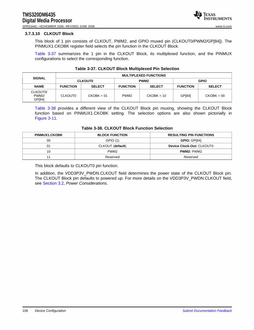
3.7.3.10 CLKOUT Block
TMS320DM6435Digital Media ProcessorSPRS344C–NOVEMBER 2006–REVISED JUNE 2008 www.ti.com
This block of 1 pin consists of CLKOUT, PWM2, and GPIO muxed pin (CLKOUT0/PWM2/GP[84]). ThePINMUX1.CKOBK register field selects the pin function in the CLKOUT Block.
Table 3-37 summarizes the 1 pin in the CLKOUT Block, its multiplexed function, and the PINMUXconfigurations to select the corresponding function.
Table 3-37. CLKOUT Block Multiplexed Pin SelectionMULTIPLEXED FUNCTIONS
SIGNALCLKOUT0 PWM2 GPIO
NAME FUNCTION SELECT FUNCTION SELECT FUNCTION SELECTCLKOUT0/
PWM2/ CLKOUT0 CKOBK = 01 PWM2 CKOBK = 10 GP[84] CKOBK = 00GP[84]
Table 3-38 provides a different view of the CLKOUT Block pin muxing, showing the CLKOUT Blockfunction based on PINMUX1.CKOBK setting. The selection options are also shown pictorially inFigure 3-11.
Table 3-38. CLKOUT Block Function SelectionPINMUX1.CKOBK BLOCK FUNCTION RESULTING PIN FUNCTIONS
00 GPIO (1) GPIO: GP[84]01 CLKOUT (default) Device Clock-Out: CLKOUT010 PWM2 PWM2: PWM211 Reserved Reserved
This block defaults to CLKOUT0 pin function.
In addition, the VDD3P3V_PWDN.CLKOUT field determines the power state of the CLKOUT Block pin.The CLKOUT Block pin defaults to powered up. For more details on the VDD3P3V_PWDN.CLKOUT field,see Section 3.2, Power Considerations.
Device Configuration106 Submit Documentation Feedback
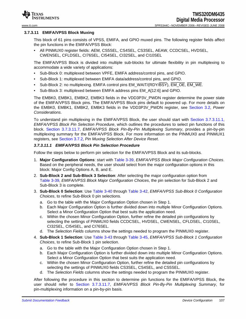
3.7.3.11 EMIFA/VPSS Block Muxing
TMS320DM6435Digital Media Processor
www.ti.com SPRS344C–NOVEMBER 2006–REVISED JUNE 2008
This block of 61 pins consists of VPSS, EMIFA, and GPIO muxed pins. The following register fields affectthe pin functions in the EMIFA/VPSS Block:• All PINMUX0 register fields: AEM, CS5SEL, CS4SEL, CS3SEL, AEAW, CCDCSEL, HVDSEL,
CWENSEL, CFLDSEL, CI76SEL, CI54SEL, CI32SEL, and CI10SEL
The EMIFA/VPSS Block is divided into multiple sub-blocks for ultimate flexibility in pin multiplexing toaccommodate a wide variety of applications:• Sub-Block 0: multiplexed between VPFE, EMIFA address/control pins, and GPIO.• Sub-Block 1: multiplexed between EMIFA data/address/control pins, and GPIO.• Sub-Block 2: no multiplexing. EMIFA control pins EM_WAIT/(RDY/BSY), EM_OE, EM_WE.• Sub-Block 3: multiplexed between EMIFA address pins EM_A[12:6] and GPIO.
The EMBK0, EMBK1, EMBK2, EMBK3 fields in the VDD3P3V_PWDN register determine the power stateof the EMIFA/VPSS Block pins. The EMIFA/VPSS Block pins default to powered up. For more details onthe EMBK0, EMBK1, EMBK2, EMBK3 fields in the VDD3P3V_PWDN register, see Section 3.2, PowerConsiderations.
To understand pin multiplexing in the EMIFA/VPSS Block, the user should start with Section 3.7.3.11.1,EMIFA/VPSS Block Pin Selection Procedure, which outlines the procedures to select pin functions of thisblock. Section 3.7.3.11.7, EMIFA/VPSS Block Pin-By-Pin Multiplexing Summary, provides a pin-by-pinmultiplexing summary for the EMIFA/VPSS Block. For more information on the PINMUX0 and PINMUX1registers, see Section 3.7.2, Pin Muxing Selection After Device Reset.3.7.3.11.1 EMIFA/VPSS Block Pin Selection Procedure
Follow the steps below to perform pin selection for the EMIFA/VPSS Block and its sub-blocks.
1. Major Configuration Options: start with Table 3-39, EMIFA/VPSS Block Major Configuration Choices.Based on the peripheral needs, the user should select from the major configuration options in thisblock: Major Config Options A, B, and E.
2. Sub-Block 2 and Sub-Block 3 Selection: After selecting the major configuration option fromTable 3-39, EMIFA/VPSS Block Major Configuration Choices, the pin selection for Sub-Block 2 andSub-Block 3 is complete.
3. Sub-Block 0 Selection: Use Table 3-40 through Table 3-42, EMIFA/VPSS Sub-Block 0 ConfigurationChoices, to refine Sub-Block 0 pin selections.a. Go to the table with the Major Configuration Option chosen in Step 1.b. Each Major Configuration Option is further divided down into multiple Minor Configuration Options.
Select a Minor Configuration Option that best suits the application need.c. Within the chosen Minor Configuration Option, further refine the detailed pin configurations by
selecting the settings of PINMUX0 fields CCDCSEL, HVDSEL, CWENSEL, CFLDSEL, CI10SEL,CI32SEL, CI54SEL, and CI76SEL.
d. The Selection Fields columns show the settings needed to program the PINMUX0 register.4. Sub-Block 1 Selection: Use Table 3-43 through Table 3-45, EMIFA/VPSS Sub-Block 1 Configuration
Choices, to refine Sub-Block 1 pin selection.a. Go to the table with the Major Configuration Option chosen in Step 1.b. Each Major Configuration Option is further divided down into multiple Minor Configuration Options.
Select a Minor Configuration Option that best suits the application need.c. Within the chosen Minor Configuration Option, further refine the detailed pin configurations by
selecting the settings of PINMUX0 fields CS3SEL, CS4SEL, and CS5SEL.d. The Selection Fields columns show the settings needed to program the PINMUX0 register.
After following the procedure in this section to determine pin functions for the EMIFA/VPSS Block, theuser should refer to Section 3.7.3.11.7, EMIFA/VPSS Block Pin-By-Pin Multiplexing Summary, forpin-multiplexing information on a pin-by-pin basis.
Submit Documentation Feedback Device Configuration 107
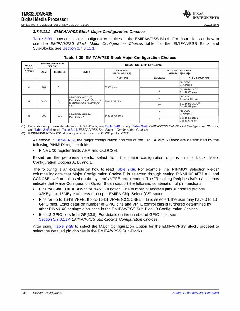
TMS320DM6435Digital Media ProcessorSPRS344C–NOVEMBER 2006–REVISED JUNE 2008 www.ti.com
3.7.3.11.2 EMIFA/VPSS Block Major Configuration Choices
Table 3-39 shows the major configuration choices in the EMIFA/VPSS Block. For instructions on how touse the EMIFA/VPSS Block Major Configuration Choices table for the EMIFA/VPSS Block andSub-Blocks, see Section 3.7.3.11.1.
Table 3-39. EMIFA/VPSS Block Major Configuration ChoicesPINMUX SELECTION RESULTING PERIPHERALS/PINSMAJOR FIELDS (1)
CONFIG.# GP PINS VPFE AND # GP PINSOPTION AEM CCDCSEL EMIFA (FROM GP[33:5]) (FROM GP[54:34])
# GP Pins CCDCSEL VPFE & # GP Pins
No CCDC0 21 GP pinsA 000 0, 1 - 29 GP pins
8-to-16-bit CCDC1 0-to-12 GP pins
No CCDC8-bit EMIFA (ASYNC) 0 11-to-19 GP pinsPinout Mode 1 with address pinsB 001 (2) 0, 1 9-to-13 GP pinsto support 32KB to 16MB per 8-to-16-bit CCDC(2)1(2)CS. 0-to-10 GP pins
No CCDC0 21 GP pins8-bit EMIFA (NAND)E 101 0, 1 14-to-18 GP pinsPinout Mode 5 8-to-16-bit CCDC1 0-to-12 GP pins
(1) For additional pin mux details for each Sub-Block, see Table 3-40 through Table 3-42, EMIFA/VPSS Sub-Block 0 Configuration Choices,and Table 3-43 through Table 3-45, EMIFA/VPSS Sub-Block 1 Configuration Choices.
(2) If PINMUX0.AEM = 001, it is not possible to get the C_WE pin for VPFE.
As shown in Table 3-39, the major configuration choices of the EMIFA/VPSS Block are determined by thefollowing PINMUX register fields:• PINMUX0 register fields AEM and CCDCSEL
Based on the peripheral needs, select from the major configuration options in this block: MajorConfiguration Options A, B, and E.
The following is an example on how to read Table 3-39. For example, the "PINMUX Selection Fields"columns indicate that Major Configuration Choice B is selected through setting PINMUX0.AEM = 1 andCCDCSEL = 0 or 1 (based on the system's VPFE requirement). The "Resulting Peripherals/Pins" columnsindicate that Major Configuration Option B can support the following combination of pin functions:• Pins for 8-bit EMIFA (Async or NAND) function. The number of address pins supported provide
32KByte to 16MByte address reach per EMIFA Chip Select (CS) space.• Pins for up to 16-bit VPFE. If 8-to-16-bit VPFE (CCDCSEL = 1) is selected, the user may have 0 to 10
GPIO pins. Exact detail on number of GPIO pins and VPFE control pins is furthered determined byother PINMUX0 settings discussed in the EMIFA/VPSS Sub-Block 0 Configuration Choices.
• 9-to-13 GPIO pins from GP[33:5]. For details on the number of GPIO pins, seeSection 3.7.3.11.4,EMIFA/VPSS Sub-Block 1 Configuration Choices.
After using Table 3-39 to select the Major Configuration Option for the EMIFA/VPSS Block, proceed toselect the detailed pin choices in the EMIFA/VPSS Sub-Blocks.
Device Configuration108 Submit Documentation Feedback
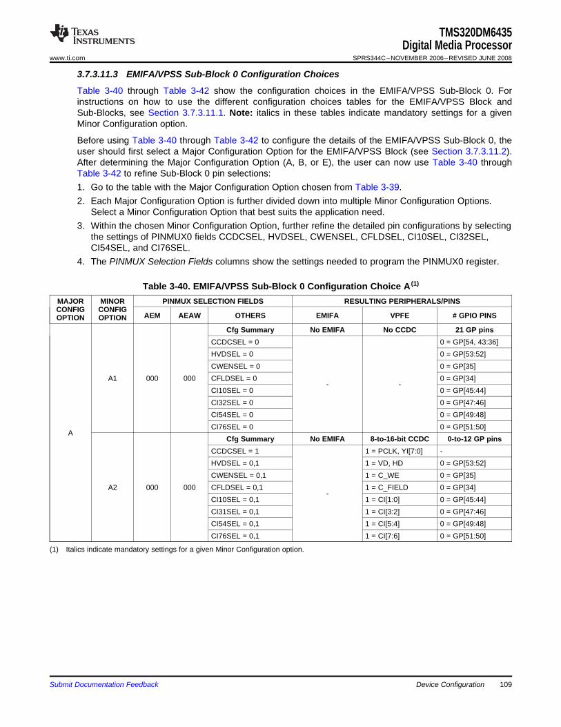
TMS320DM6435Digital Media Processor
www.ti.com SPRS344C–NOVEMBER 2006–REVISED JUNE 2008
3.7.3.11.3 EMIFA/VPSS Sub-Block 0 Configuration Choices
Table 3-40 through Table 3-42 show the configuration choices in the EMIFA/VPSS Sub-Block 0. Forinstructions on how to use the different configuration choices tables for the EMIFA/VPSS Block andSub-Blocks, see Section 3.7.3.11.1. Note: italics in these tables indicate mandatory settings for a givenMinor Configuration option.
Before using Table 3-40 through Table 3-42 to configure the details of the EMIFA/VPSS Sub-Block 0, theuser should first select a Major Configuration Option for the EMIFA/VPSS Block (see Section 3.7.3.11.2).After determining the Major Configuration Option (A, B, or E), the user can now use Table 3-40 throughTable 3-42 to refine Sub-Block 0 pin selections:1. Go to the table with the Major Configuration Option chosen from Table 3-39.2. Each Major Configuration Option is further divided down into multiple Minor Configuration Options.
Select a Minor Configuration Option that best suits the application need.3. Within the chosen Minor Configuration Option, further refine the detailed pin configurations by selecting
the settings of PINMUX0 fields CCDCSEL, HVDSEL, CWENSEL, CFLDSEL, CI10SEL, CI32SEL,CI54SEL, and CI76SEL.
4. The PINMUX Selection Fields columns show the settings needed to program the PINMUX0 register.
Table 3-40. EMIFA/VPSS Sub-Block 0 Configuration Choice A (1)
MAJOR MINOR PINMUX SELECTION FIELDS RESULTING PERIPHERALS/PINSCONFIG CONFIG
AEM AEAW OTHERS EMIFA VPFE # GPIO PINSOPTION OPTIONCfg Summary No EMIFA No CCDC 21 GP pins
CCDCSEL = 0 0 = GP[54, 43:36]HVDSEL = 0 0 = GP[53:52]CWENSEL = 0 0 = GP[35]
A1 000 000 CFLDSEL = 0 0 = GP[34]- -
CI10SEL = 0 0 = GP[45:44]CI32SEL = 0 0 = GP[47:46]CI54SEL = 0 0 = GP[49:48]CI76SEL = 0 0 = GP[51:50]
ACfg Summary No EMIFA 8-to-16-bit CCDC 0-to-12 GP pins
CCDCSEL = 1 1 = PCLK, YI[7:0] -HVDSEL = 0,1 1 = VD, HD 0 = GP[53:52]CWENSEL = 0,1 1 = C_WE 0 = GP[35]
A2 000 000 CFLDSEL = 0,1 1 = C_FIELD 0 = GP[34]-
CI10SEL = 0,1 1 = CI[1:0] 0 = GP[45:44]CI31SEL = 0,1 1 = CI[3:2] 0 = GP[47:46]CI54SEL = 0,1 1 = CI[5:4] 0 = GP[49:48]CI76SEL = 0,1 1 = CI[7:6] 0 = GP[51:50]
(1) Italics indicate mandatory settings for a given Minor Configuration option.
Submit Documentation Feedback Device Configuration 109
TMS320DM6435Digital Media ProcessorSPRS344C–NOVEMBER 2006–REVISED JUNE 2008 www.ti.com
Table 3-41. EMIFA/VPSS Sub-Block 0 Configuration Choice B (1)
MAJOR MINOR PINMUX SELECTION FIELDS RESULTING PERIPHERALS/PINSCONFIG CONFIG
AEM AEAW OTHERS EMIFA VPFE # GPIO PINSOPTION OPTION8-bit EMIFA
(Async) PinoutConfig Summary No CCDC 11 GP pinsmode 1 w/EM_A[21:0]
CCDCSEL = 0 - 0 = GP[54, 43:36]HVDSEL = 0 - 0 = GP[53:52]
B B1 001 100 CWENSEL = 0 0 = EM_R/W -CFLDSEL = 0 0 = EM_A21 -
-CI10SEL = 0 0 = EM_A[19:20] -CI32SEL = 0 0 = EM_A[17:18] -CI54SEL = 0 0 = EM_A[15:16] -CI76SEL = 0 0 = EM_A[13:14] -
8-bit EMIFA(Async) PinoutConfig Summary 8-to-16-bit CCDC 0-to-10 GP pinsmode 1 w/
EM_A[12:0] onlyCCDCSEL = 1 - 1 = PCLK, YI[7:0] -HVDSEL = 0,1 - 1 = VD, HD 0 = GP[53:52]CWENSEL = 0 0 = EM_R/W - -B B2 001 000
0 = EM_A21CFLDSEL = 0,1 1 = C_FIELD -(not used)CI10SEL = 0,1 - 1 = CI[1:0] 0 = GP[45:44]CI32SEL = 0,1 - 1 = CI[3:2] 0 = GP[47:46]CI54SEL = 0,1 - 1 = CI[5:4] 0 = GP[49:48]CI76SEL = 0,1 - 1 = CI[7:6] 0 = GP[51:50]
8-bit EMIFA(Async) PinoutConfig Summary 8-to-14-bit CCDC 0-to-8 GP pinsmode 1 w/
EM_A[14:0] onlyCCDCSEL = 1 - 1 = PCLK, YI[7:0] -HVDSEL = 0,1 - 1 = VD, HD 0 = GP[53:52]CWENSEL = 0 0 = EM_R/W - -B B3 001 001
0 = EM_A21CFLDSEL = 0,1 1 = C_FIELD -(not used)CI10SEL = 0,1 - 1 = CI[1:0] 0 = GP[45:44]CI32SEL = 0,1 - 1 = CI[3:2] 0 = GP[47:46]CI54SEL = 0,1 - 1 = CI[5:4] 0 = GP[49:48]CI76SEL = 0 0 = EM_A[13:14] - -
(1) Italics indicate mandatory settings for a given Minor Configuration option.
110 Device Configuration Submit Documentation Feedback
TMS320DM6435Digital Media Processor
www.ti.com SPRS344C–NOVEMBER 2006–REVISED JUNE 2008
Table 3-41. EMIFA/VPSS Sub-Block 0 Configuration Choice B (continued)MAJOR MINOR PINMUX SELECTION FIELDS RESULTING PERIPHERALS/PINSCONFIG CONFIG
AEM AEAW OTHERS EMIFA VPFE # GPIO PINSOPTION OPTION8-bit EMIFA
(Async) PinoutConfig Summary 8-to-12-bit CCDC 0-to-6 GP pinsmode 1 w/EM_A[16:0] only
CCDCSEL = 1 - 1 = PCLK, YI[7:0] -HVDSEL = 0,1 - 1 = VD, HD 0 = GP[53:52]CWENSEL = 0 0 = EM_R/W - -B B4 001 010
0 = EM_A21CFLDSEL = 0,1 1 = C_FIELD -(not used)CI10SEL = 0,1 - 1 = CI[1:0] 0 = GP[45:44]CI32SEL = 0,1 - 1 = CI[3:2] 0 = GP[47:46]CI54SEL = 0 0 = EM_A[15:16] - -CI76SEL = 0 0 = EM_A[13:14] - -
8-bit EMIFA(Async) PinoutConfig Summary 8-to-10-bit CCDC 0-to-4 GP pinsmode 1 w/
EM_A[18:0] onlyCCDCSEL = 1 - 1 = PCLK, YI[7:0] -HVDSEL = 0,1 - 1 = VD, HD 0 = GP[53:52]CWENSEL = 0 0 = EM_R/W - -B B5 001 011
0 = EM_A21CFLDSEL = 0,1 1 = C_FIELD -(not used)CI10SEL = 0,1 - 1 = CI[1:0] 0 = GP[45:44]CI32SEL = 0 0 = EM_A[17:18] - -CI54SEL = 0 0 = EM_A[15:16] - -CI76SEL = 0 0 = EM_A[13:14] - -
Submit Documentation Feedback Device Configuration 111
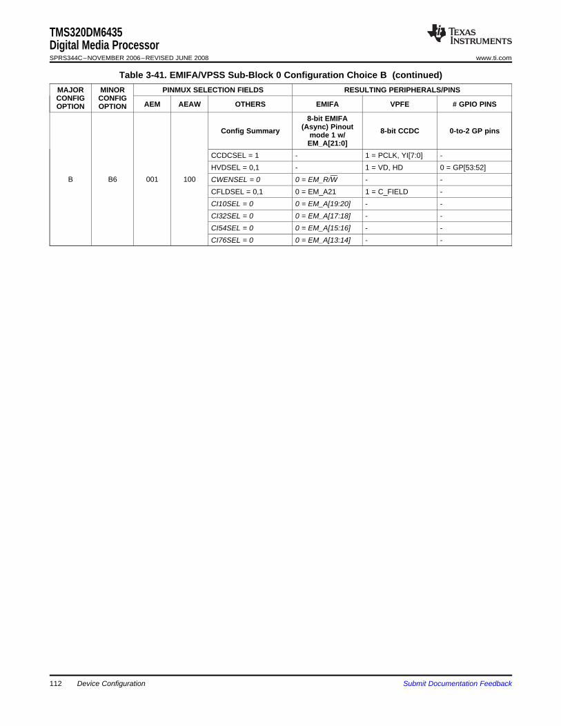
TMS320DM6435Digital Media ProcessorSPRS344C–NOVEMBER 2006–REVISED JUNE 2008 www.ti.com
Table 3-41. EMIFA/VPSS Sub-Block 0 Configuration Choice B (continued)MAJOR MINOR PINMUX SELECTION FIELDS RESULTING PERIPHERALS/PINSCONFIG CONFIG
AEM AEAW OTHERS EMIFA VPFE # GPIO PINSOPTION OPTION8-bit EMIFA
(Async) PinoutConfig Summary 8-bit CCDC 0-to-2 GP pinsmode 1 w/EM_A[21:0]
CCDCSEL = 1 - 1 = PCLK, YI[7:0] -HVDSEL = 0,1 - 1 = VD, HD 0 = GP[53:52]
B B6 001 100 CWENSEL = 0 0 = EM_R/W - -CFLDSEL = 0,1 0 = EM_A21 1 = C_FIELD -CI10SEL = 0 0 = EM_A[19:20] - -CI32SEL = 0 0 = EM_A[17:18] - -CI54SEL = 0 0 = EM_A[15:16] - -CI76SEL = 0 0 = EM_A[13:14] - -
Device Configuration112 Submit Documentation Feedback
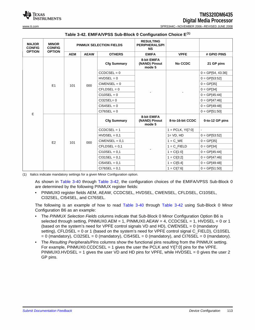
TMS320DM6435Digital Media Processor
www.ti.com SPRS344C–NOVEMBER 2006–REVISED JUNE 2008
Table 3-42. EMIFA/VPSS Sub-Block 0 Configuration Choice E (1)
RESULTINGMAJOR MINOR PINMUX SELECTION FIELDS PERIPHERALS/PICONFIG CONFIG NSOPTION OPTION
AEM AEAW OTHERS EMIFA VPFE # GPIO PINS8-bit EMIFA
Cfg Summary (NAND) Pinout No CCDC 21 GP pinsmode 5
CCDCSEL = 0 0 = GP[54, 43:36]HVDSEL = 0 0 = GP[53:52]CWENSEL = 0 0 = GP[35]E1 101 000CFLDSEL = 0 0 = GP[34]
- -CI10SEL = 0 0 = GP[45:44]CI32SEL= 0 0 = GP[47:46]CI54SEL = 0 0 = GP[49:48]CI76SEL = 0 0 = GP[51:50]
E8-bit EMIFA
Cfg Summary (NAND) Pinout 8-to-16-bit CCDC 0-to-12 GP pinsmode 5
CCDCSEL = 1 1 = PCLK, YI[7:0] -HVDSEL = 0,1 1= VD, HD 0 = GP[53:52]CWENSEL = 0,1 1 = C_WE 0 = GP[35]E2 101 000CFLDSEL = 0,1 1 = C_FIELD 0 = GP[34]
-CI10SEL = 0,1 1 = CI[1:0] 0 = GP[45:44]CI31SEL = 0,1 1 = CI[3:2] 0 = GP[47:46]CI54SEL = 0,1 1 = CI[5:4] 0 = GP[49:48]CI76SEL = 0,1 1 = CI[7:6] 0 = GP[51:50]
(1) Italics indicate mandatory settings for a given Minor Configuration option.
As shown in Table 3-40 through Table 3-42, the configuration choices of the EMIFA/VPSS Sub-Block 0are determined by the following PINMUX register fields:• PINMUX0 register fields AEM, AEAW, CCDCSEL, HVDSEL, CWENSEL, CFLDSEL, CI10SEL,
CI32SEL, CI54SEL, and CI76SEL.
The following is an example of how to read Table 3-40 through Table 3-42 using Sub-Block 0 MinorConfiguration B6 as an example:• The PINMUX Selection Fields columns indicate that Sub-Block 0 Minor Configuration Option B6 is
selected through setting, PINMUX0.AEM = 1, PINMUX0.AEAW = 4, CCDCSEL = 1, HVDSEL = 0 or 1(based on the system’s need for VPFE control signals VD and HD), CWENSEL = 0 (mandatorysetting), CFLDSEL = 0 or 1 (based on the system’s need for VPFE control signal C_FIELD), CI10SEL= 0 (mandatory), CI32SEL = 0 (mandatory), CI54SEL = 0 (mandatory), and CI76SEL = 0 (mandatory).
• The Resulting Peripherals/Pins columns show the functional pins resulting from the PINMUX setting.For example, PINMUX0.CCDCSEL = 1 gives the user the PCLK and YI[7:0] pins for the VPFE.PINMUX0.HVDSEL = 1 gives the user VD and HD pins for VPFE, while HVDSEL = 0 gives the user 2GP pins.
Submit Documentation Feedback Device Configuration 113
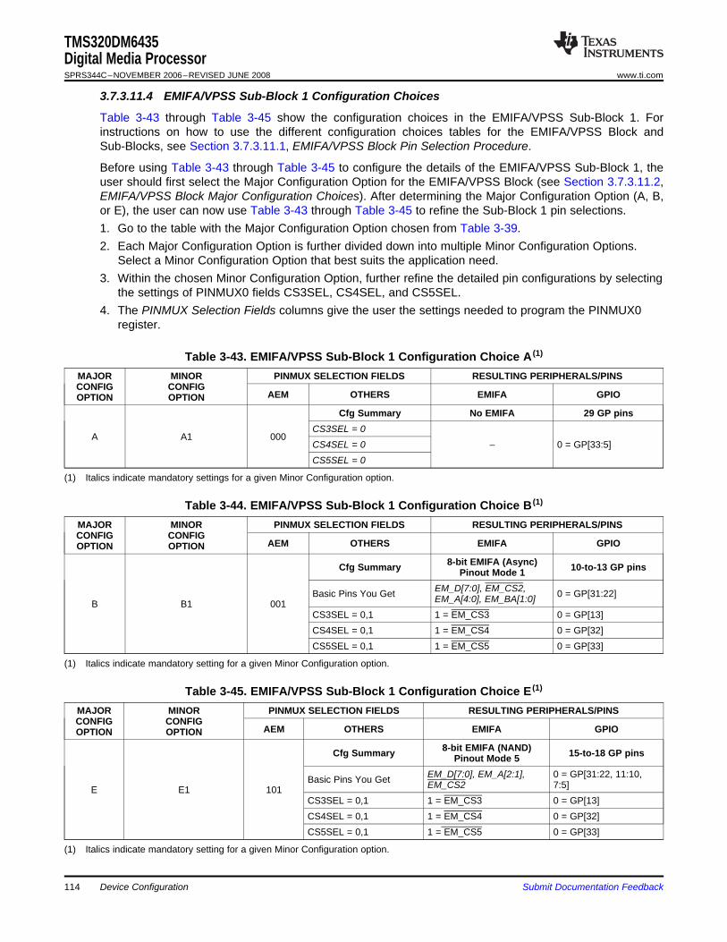
TMS320DM6435Digital Media ProcessorSPRS344C–NOVEMBER 2006–REVISED JUNE 2008 www.ti.com
3.7.3.11.4 EMIFA/VPSS Sub-Block 1 Configuration Choices
Table 3-43 through Table 3-45 show the configuration choices in the EMIFA/VPSS Sub-Block 1. Forinstructions on how to use the different configuration choices tables for the EMIFA/VPSS Block andSub-Blocks, see Section 3.7.3.11.1, EMIFA/VPSS Block Pin Selection Procedure.
Before using Table 3-43 through Table 3-45 to configure the details of the EMIFA/VPSS Sub-Block 1, theuser should first select the Major Configuration Option for the EMIFA/VPSS Block (see Section 3.7.3.11.2,EMIFA/VPSS Block Major Configuration Choices). After determining the Major Configuration Option (A, B,or E), the user can now use Table 3-43 through Table 3-45 to refine the Sub-Block 1 pin selections.1. Go to the table with the Major Configuration Option chosen from Table 3-39.2. Each Major Configuration Option is further divided down into multiple Minor Configuration Options.
Select a Minor Configuration Option that best suits the application need.3. Within the chosen Minor Configuration Option, further refine the detailed pin configurations by selecting
the settings of PINMUX0 fields CS3SEL, CS4SEL, and CS5SEL.4. The PINMUX Selection Fields columns give the user the settings needed to program the PINMUX0
register.
Table 3-43. EMIFA/VPSS Sub-Block 1 Configuration Choice A (1)
MAJOR MINOR PINMUX SELECTION FIELDS RESULTING PERIPHERALS/PINSCONFIG CONFIG
AEM OTHERS EMIFA GPIOOPTION OPTIONCfg Summary No EMIFA 29 GP pins
CS3SEL = 0A A1 000
CS4SEL = 0 – 0 = GP[33:5]CS5SEL = 0
(1) Italics indicate mandatory settings for a given Minor Configuration option.
Table 3-44. EMIFA/VPSS Sub-Block 1 Configuration Choice B (1)
MAJOR MINOR PINMUX SELECTION FIELDS RESULTING PERIPHERALS/PINSCONFIG CONFIG
AEM OTHERS EMIFA GPIOOPTION OPTION8-bit EMIFA (Async)Cfg Summary 10-to-13 GP pinsPinout Mode 1
EM_D[7:0], EM_CS2,Basic Pins You Get 0 = GP[31:22]EM_A[4:0], EM_BA[1:0]B B1 001CS3SEL = 0,1 1 = EM_CS3 0 = GP[13]CS4SEL = 0,1 1 = EM_CS4 0 = GP[32]CS5SEL = 0,1 1 = EM_CS5 0 = GP[33]
(1) Italics indicate mandatory setting for a given Minor Configuration option.
Table 3-45. EMIFA/VPSS Sub-Block 1 Configuration Choice E (1)
MAJOR MINOR PINMUX SELECTION FIELDS RESULTING PERIPHERALS/PINSCONFIG CONFIG
AEM OTHERS EMIFA GPIOOPTION OPTION8-bit EMIFA (NAND)Cfg Summary 15-to-18 GP pinsPinout Mode 5
EM_D[7:0], EM_A[2:1], 0 = GP[31:22, 11:10,Basic Pins You Get EM_CS2 7:5]E E1 101CS3SEL = 0,1 1 = EM_CS3 0 = GP[13]CS4SEL = 0,1 1 = EM_CS4 0 = GP[32]CS5SEL = 0,1 1 = EM_CS5 0 = GP[33]
(1) Italics indicate mandatory setting for a given Minor Configuration option.
Device Configuration114 Submit Documentation Feedback
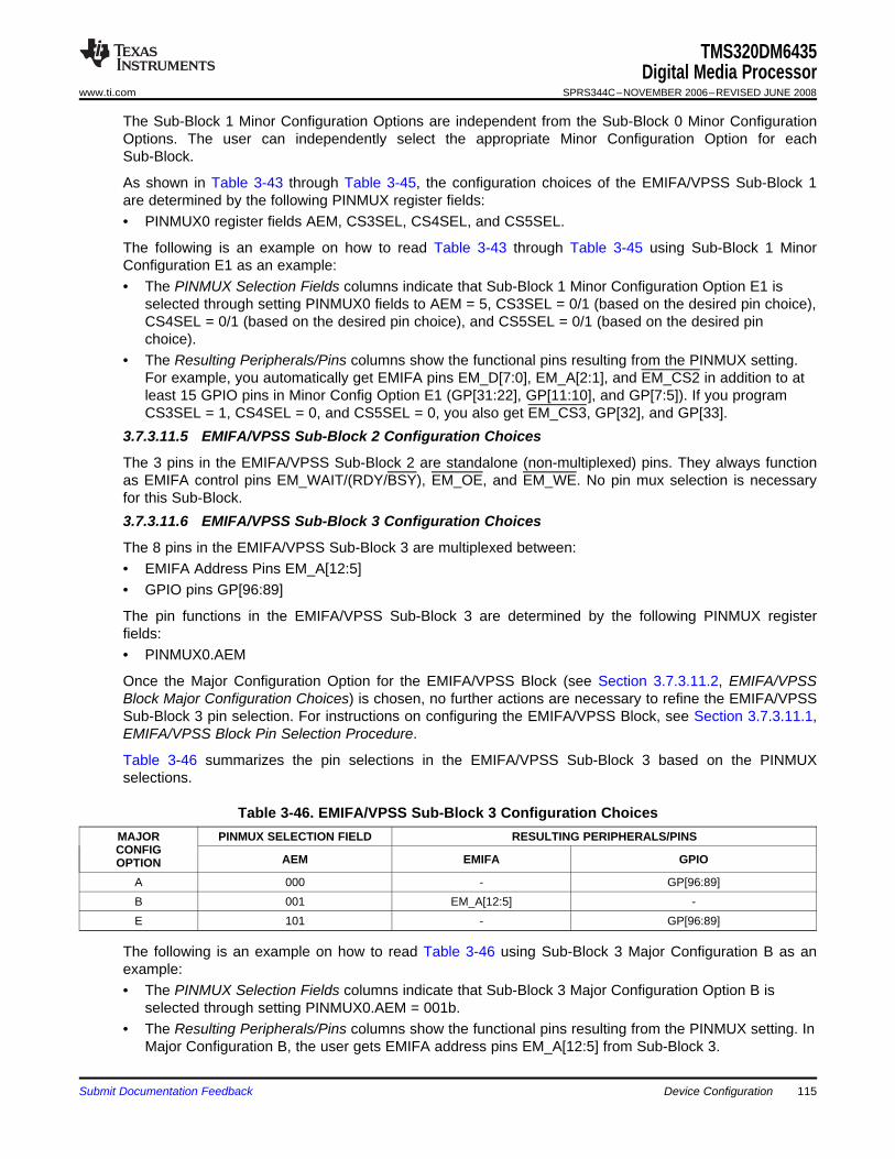
TMS320DM6435Digital Media Processor
www.ti.com SPRS344C–NOVEMBER 2006–REVISED JUNE 2008
The Sub-Block 1 Minor Configuration Options are independent from the Sub-Block 0 Minor ConfigurationOptions. The user can independently select the appropriate Minor Configuration Option for eachSub-Block.
As shown in Table 3-43 through Table 3-45, the configuration choices of the EMIFA/VPSS Sub-Block 1are determined by the following PINMUX register fields:• PINMUX0 register fields AEM, CS3SEL, CS4SEL, and CS5SEL.
The following is an example on how to read Table 3-43 through Table 3-45 using Sub-Block 1 MinorConfiguration E1 as an example:• The PINMUX Selection Fields columns indicate that Sub-Block 1 Minor Configuration Option E1 is
selected through setting PINMUX0 fields to AEM = 5, CS3SEL = 0/1 (based on the desired pin choice),CS4SEL = 0/1 (based on the desired pin choice), and CS5SEL = 0/1 (based on the desired pinchoice).
• The Resulting Peripherals/Pins columns show the functional pins resulting from the PINMUX setting.For example, you automatically get EMIFA pins EM_D[7:0], EM_A[2:1], and EM_CS2 in addition to atleast 15 GPIO pins in Minor Config Option E1 (GP[31:22], GP[11:10], and GP[7:5]). If you programCS3SEL = 1, CS4SEL = 0, and CS5SEL = 0, you also get EM_CS3, GP[32], and GP[33].
3.7.3.11.5 EMIFA/VPSS Sub-Block 2 Configuration Choices
The 3 pins in the EMIFA/VPSS Sub-Block 2 are standalone (non-multiplexed) pins. They always functionas EMIFA control pins EM_WAIT/(RDY/BSY), EM_OE, and EM_WE. No pin mux selection is necessaryfor this Sub-Block.3.7.3.11.6 EMIFA/VPSS Sub-Block 3 Configuration Choices
The 8 pins in the EMIFA/VPSS Sub-Block 3 are multiplexed between:• EMIFA Address Pins EM_A[12:5]• GPIO pins GP[96:89]
The pin functions in the EMIFA/VPSS Sub-Block 3 are determined by the following PINMUX registerfields:• PINMUX0.AEM
Once the Major Configuration Option for the EMIFA/VPSS Block (see Section 3.7.3.11.2, EMIFA/VPSSBlock Major Configuration Choices) is chosen, no further actions are necessary to refine the EMIFA/VPSSSub-Block 3 pin selection. For instructions on configuring the EMIFA/VPSS Block, see Section 3.7.3.11.1,EMIFA/VPSS Block Pin Selection Procedure.
Table 3-46 summarizes the pin selections in the EMIFA/VPSS Sub-Block 3 based on the PINMUXselections.
Table 3-46. EMIFA/VPSS Sub-Block 3 Configuration ChoicesMAJOR PINMUX SELECTION FIELD RESULTING PERIPHERALS/PINSCONFIG
AEM EMIFA GPIOOPTIONA 000 - GP[96:89]B 001 EM_A[12:5] -E 101 - GP[96:89]
The following is an example on how to read Table 3-46 using Sub-Block 3 Major Configuration B as anexample:• The PINMUX Selection Fields columns indicate that Sub-Block 3 Major Configuration Option B is
selected through setting PINMUX0.AEM = 001b.• The Resulting Peripherals/Pins columns show the functional pins resulting from the PINMUX setting. In
Major Configuration B, the user gets EMIFA address pins EM_A[12:5] from Sub-Block 3.
Submit Documentation Feedback Device Configuration 115
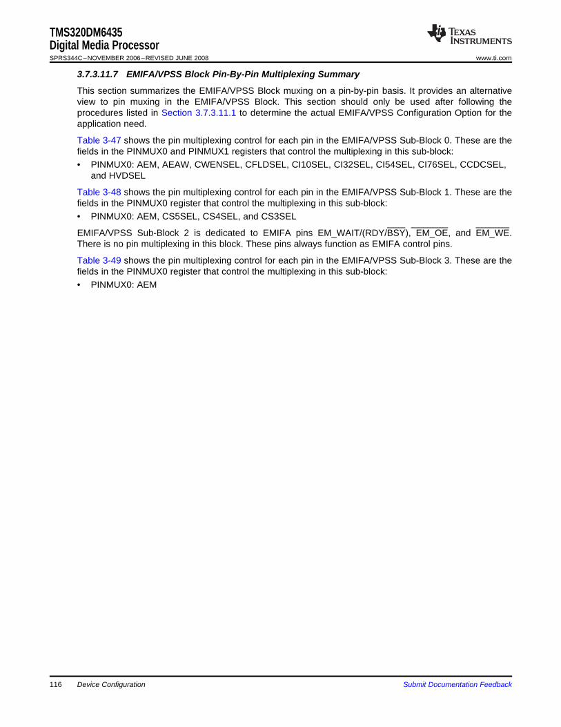
TMS320DM6435Digital Media ProcessorSPRS344C–NOVEMBER 2006–REVISED JUNE 2008 www.ti.com
3.7.3.11.7 EMIFA/VPSS Block Pin-By-Pin Multiplexing Summary
This section summarizes the EMIFA/VPSS Block muxing on a pin-by-pin basis. It provides an alternativeview to pin muxing in the EMIFA/VPSS Block. This section should only be used after following theprocedures listed in Section 3.7.3.11.1 to determine the actual EMIFA/VPSS Configuration Option for theapplication need.
Table 3-47 shows the pin multiplexing control for each pin in the EMIFA/VPSS Sub-Block 0. These are thefields in the PINMUX0 and PINMUX1 registers that control the multiplexing in this sub-block:• PINMUX0: AEM, AEAW, CWENSEL, CFLDSEL, CI10SEL, CI32SEL, CI54SEL, CI76SEL, CCDCSEL,
and HVDSEL
Table 3-48 shows the pin multiplexing control for each pin in the EMIFA/VPSS Sub-Block 1. These are thefields in the PINMUX0 register that control the multiplexing in this sub-block:• PINMUX0: AEM, CS5SEL, CS4SEL, and CS3SEL
EMIFA/VPSS Sub-Block 2 is dedicated to EMIFA pins EM_WAIT/(RDY/BSY), EM_OE, and EM_WE.There is no pin multiplexing in this block. These pins always function as EMIFA control pins.
Table 3-49 shows the pin multiplexing control for each pin in the EMIFA/VPSS Sub-Block 3. These are thefields in the PINMUX0 register that control the multiplexing in this sub-block:• PINMUX0: AEM
116 Device Configuration Submit Documentation Feedback
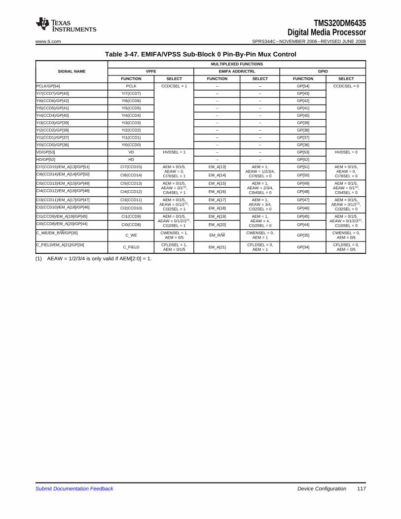
TMS320DM6435Digital Media Processor
www.ti.com SPRS344C–NOVEMBER 2006–REVISED JUNE 2008
Table 3-47. EMIFA/VPSS Sub-Block 0 Pin-By-Pin Mux ControlMULTIPLEXED FUNCTIONS
SIGNAL NAME VPFE EMIFA ADDR/CTRL GPIO
FUNCTION SELECT FUNCTION SELECT FUNCTION SELECT
PCLK/GP[54] PCLK CCDCSEL = 1 – – GP[54] CCDCSEL = 0
YI7(CCD7)/GP[43] YI7(CCD7) – – GP[43]
YI6(CCD6)/GP[42] YI6(CCD6) – – GP[42]
YI5(CCD5)/GP[41] YI5(CCD5) – – GP[41]
YI4(CCD4)/GP[40] YI4(CCD4) – – GP[40]
YI3(CCD3)/GP[39] YI3(CCD3) – – GP[39]
YI2(CCD2)/GP[38] YI2(CCD2) – – GP[38]
YI1(CCD1)/GP[37] YI1(CCD1) – – GP[37]
YI0(CCD0)/GP[36] YI0(CCD0) – – GP[36]
VD/GP[53] VD HVDSEL = 1 – – GP[53] HVDSEL = 0
HD/GP[52] HD – – GP[52]
CI7(CCD15)/EM_A[13]/GP[51] CI7(CCD15) AEM = 0/1/5, EM_A[13] AEM = 1, GP[51] AEM = 0/1/5,AEAW = 0, AEAW = 1/2/3/4, AEAW = 0,
CI6(CCD14)/EM_A[14]/GP[50] CI6(CCD14) EM_A[14] GP[50]CI76SEL = 1 CI76SEL = 0 CI76SEL = 0
CI5(CCD13)/EM_A[15]/GP[49] CI5(CCD13) AEM = 0/1/5, EM_A[15] AEM = 1, GP[49] AEM = 0/1/5,AEAW = 0/1 (1), AEAW = 2/3/4, AEAW = 0/1(1),
CI4(CCD12)/EM_A[16]/GP[48] CI4(CCD12) EM_A[16] GP[48]CI54SEL = 1 CI54SEL = 0 CI54SEL = 0
CI3(CCD11)/EM_A[17]/GP[47] CI3(CCD11) AEM = 0/1/5, EM_A[17] AEM = 1, GP[47] AEM = 0/1/5,AEAW = 0/1/2(1), AEAW = 3/4, AEAW = 0/1/2(1),
CI2(CCD10)/EM_A[18]/GP[46] CI2(CCD10) EM_A[18] GP[46]CI32SEL = 1 CI32SEL = 0 CI32SEL = 0
CI1(CCD9)/EM_A[19]/GP[45] CI1(CCD9) AEM = 0/1/5, EM_A[19] AEM = 1, GP[45] AEM = 0/1/5,AEAW = 0/1/2/3(1), AEAW = 4, AEAW = 0/1/2/3(1),
CI0(CCD8)/EM_A[20]/GP[44] CI0(CCD8) EM_A[20] GP[44]CI10SEL = 1 CI10SEL = 0 CI10SEL = 0
C_WE/EM_R/W/GP[35] CWENSEL = 1, CWENSEL = 0, CWENSEL = 0,C_WE EM_R/W GP[35]AEM = 0/5 AEM = 1 AEM = 0/5
C_FIELD/EM_A[21]/GP[34] CFLDSEL = 1, CFLDSEL = 0, CFLDSEL = 0,C_FIELD EM_A[21] GP[34]AEM = 0/1/5 AEM = 1 AEM = 0/5
(1) AEAW = 1/2/3/4 is only valid if AEM[2:0] = 1.
Submit Documentation Feedback Device Configuration 117
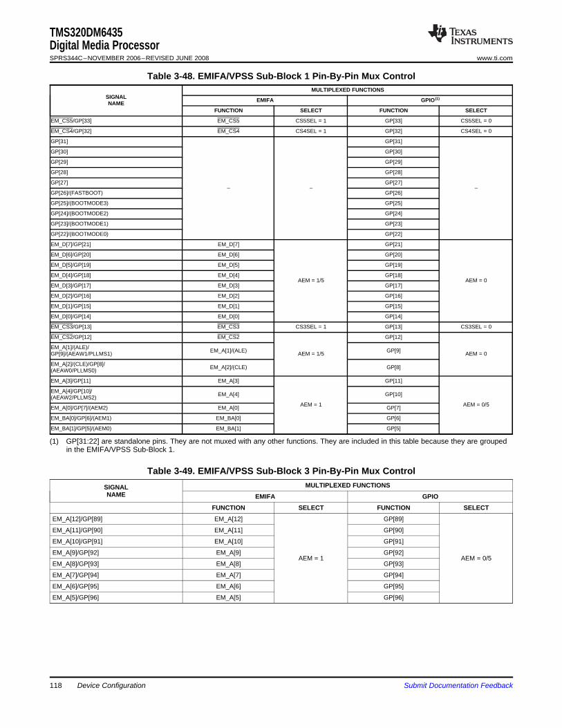
TMS320DM6435Digital Media ProcessorSPRS344C–NOVEMBER 2006–REVISED JUNE 2008 www.ti.com
Table 3-48. EMIFA/VPSS Sub-Block 1 Pin-By-Pin Mux ControlMULTIPLEXED FUNCTIONS
SIGNAL EMIFA GPIO (1)NAME
FUNCTION SELECT FUNCTION SELECT
EM_CS5/GP[33] EM_CS5 CS5SEL = 1 GP[33] CS5SEL = 0
EM_CS4/GP[32] EM_CS4 CS4SEL = 1 GP[32] CS4SEL = 0
GP[31] GP[31]
GP[30] GP[30]
GP[29] GP[29]
GP[28] GP[28]
GP[27] GP[27]– – –
GP[26]/(FASTBOOT) GP[26]
GP[25]/(BOOTMODE3) GP[25]
GP[24]/(BOOTMODE2) GP[24]
GP[23]/(BOOTMODE1) GP[23]
GP[22]/(BOOTMODE0) GP[22]
EM_D[7]/GP[21] EM_D[7] GP[21]
EM_D[6]/GP[20] EM_D[6] GP[20]
EM_D[5]/GP[19] EM_D[5] GP[19]
EM_D[4]/GP[18] EM_D[4] GP[18]AEM = 1/5 AEM = 0
EM_D[3]/GP[17] EM_D[3] GP[17]
EM_D[2]/GP[16] EM_D[2] GP[16]
EM_D[1]/GP[15] EM_D[1] GP[15]
EM_D[0]/GP[14] EM_D[0] GP[14]
EM_CS3/GP[13] EM_CS3 CS3SEL = 1 GP[13] CS3SEL = 0
EM_CS2/GP[12] EM_CS2 GP[12]
EM_A[1]/(ALE)/ EM_A[1]/(ALE) GP[9]GP[9]/(AEAW1/PLLMS1) AEM = 1/5 AEM = 0
EM_A[2]/(CLE)/GP[8]/ EM_A[2]/(CLE) GP[8](AEAW0/PLLMS0)
EM_A[3]/GP[11] EM_A[3] GP[11]
EM_A[4]/GP[10]/ EM_A[4] GP[10](AEAW2/PLLMS2)AEM = 1 AEM = 0/5EM_A[0]/GP[7]/(AEM2) EM_A[0] GP[7]
EM_BA[0]/GP[6]/(AEM1) EM_BA[0] GP[6]
EM_BA[1]/GP[5]/(AEM0) EM_BA[1] GP[5]
(1) GP[31:22] are standalone pins. They are not muxed with any other functions. They are included in this table because they are groupedin the EMIFA/VPSS Sub-Block 1.
Table 3-49. EMIFA/VPSS Sub-Block 3 Pin-By-Pin Mux ControlMULTIPLEXED FUNCTIONSSIGNAL
NAME EMIFA GPIO
FUNCTION SELECT FUNCTION SELECT
EM_A[12]/GP[89] EM_A[12] GP[89]
EM_A[11]/GP[90] EM_A[11] GP[90]
EM_A[10]/GP[91] EM_A[10] GP[91]
EM_A[9]/GP[92] EM_A[9] GP[92]AEM = 1 AEM = 0/5
EM_A[8]/GP[93] EM_A[8] GP[93]
EM_A[7]/GP[94] EM_A[7] GP[94]
EM_A[6]/GP[95] EM_A[6] GP[95]
EM_A[5]/GP[96] EM_A[5] GP[96]
Device Configuration118 Submit Documentation Feedback
3.8 Device Initialization Sequence After Reset
TMS320DM6435Digital Media Processor
www.ti.com SPRS344C–NOVEMBER 2006–REVISED JUNE 2008
Software should follow this initialization sequence after coming out of device reset.1. Complete the boot sequence as needed. For more details on the boot sequence, see the Using the
TMS320DM643x Bootloader Application Report (literature number SPRAAG0).2. If the device is not already at the desired operating frequency, program the PLL Controllers (PLLC1
and PLLC2) to configure the device frequency. For details on how to program the PLLC, see theTMS320DM643x DMP DSP Subsystem Reference Guide (literature number SPRU978).
3. Program PINMUX0 and PINMUX1 registers to select device pin functions. For more details onprogramming the PINMUX0 and PINMUX1 registers to select device pin functions, see Section 3.7,Multiplexed Pin Configurations.Note: if EMAC operation is desired, the EMAC must be placed in reset before programmingPINMUX1.HOSTBK to select EMAC pins.
4. Program the VDD3P3V_PWDN register to power up the necessary I/O pins. For more details onprogramming the VDD3P3V_PWDN register, see Section 3.2, Power Considerations. On DM6435, theuser should program VDD3P3V_PWDN bit 13 to 1 to power down the reserved pins RSV17, RSV18,and RSV19.
5. As needed by the application, program the following System Module registers when there are no activetransactions on the respective peripherals:a. HPICTL (Section 3.6.2.1, HPI Control Register): applicable for HPI only if a different host burst
write timeout value from default is desired.b. TIMERCTL (Section 3.6.2.2, Timer Control Register): applicable for Timer0 and Watchdog Timer2
only.c. EDMATCCFG (Section 3.6.2.3, EDMA TC Configuration Register): applicable for EDMA only. The
recommendation is to leave the EDMATCCFG register at its default.d. VPSS_CLKCTL (Section 3.3.2, VPSS Clocks): applicable for VPSS only.
6. Program the Power and Sleep Controller (PSC) to enable the desired peripherals. For details on howto program the PSC, see the TMS320DM643x DMP DSP Subsystem Reference Guide (literaturenumber SPRU978).
7. Program the Switched Central Resource (SCR) bus priorities for the master peripherals(Section 3.6.1). This must be configured when there are no active transactions on the respectiveperipherals:a. Program the MSTPRI0 and MSTPRI1 registers in the System Module. These registers can be
programmed before or after the respective peripheral is enabled by the PSC in step 6.b. Program the EDMACC QUEPRI register, the C64x+ MDMAARBE.PRI field, and the VPSS PCR
register. These registers can only be programmed after the respective peripheral is enabled by thePSC in step 6.
8. Configure the C64x+ Megamodule and the peripherals.a. For details on C64x+ Megamodule configuration, see the TMS320C64x+ DSP Megamodule
Reference Guide (literature number SPRU871).
Special considerations: Bootloader disables C64x+ cache—For all boot modes that default toDSPBOOTADDR = 0x0010 0000 (i.e., all boot modes except the EMIFA ROM Direct Boot,BOOTMODE[3:0] = 0100, FASTBOOT = 0), the bootloader code disables all C64x+ cache (L2,L1P, and L1D) so that upon exit from the bootloader code, all C64x+ memories are configured asall RAM (L2CFG.L2MODE = 0h, L1PCFG.L1PMODE = 0h, and L1DCFG.L1DMODE = 0h). If cacheuse is required, the application code must explicitly enable the cache. For more information on bootmodes, see Section 3.4.1, Boot Modes. For more information on the bootloader, see the Using theTMS320DM643x Bootloader Application Report (literature number SPRAAG0).
Submit Documentation Feedback Device Configuration 119
TMS320DM6435Digital Media ProcessorSPRS344C–NOVEMBER 2006–REVISED JUNE 2008 www.ti.com
b. Peripherals configuration: see the respective peripheral user’s guide.
Special considerations: DDR2 memory controller—the Peripheral Bus Burst Priority Register(PBBPR) should be programmed to ensure good DDR2 throughput and to prevent commandstarvation (prevention of certain commands from being processed by the DDR2 memory controller).For more details, see the TMS320DM643x DMP DDR2 Memory Controller User’s Guide (literaturenumber SPRU986). A hex value of 0x20 is recommended for the PBBPR PR_OLD_COUNT field toprovide a good DSP performance and still allow good utilization by other modules.
120 Device Configuration Submit Documentation Feedback

3.9 Debugging Considerations
3.9.1 Pullup/Pulldown Resistors
TMS320DM6435Digital Media Processor
www.ti.com SPRS344C–NOVEMBER 2006–REVISED JUNE 2008
Proper board design should ensure that input pins to the DM643x DMP device always be at a valid logiclevel and not floating. This may be achieved via pullup/pulldown resistors. The DM643x DMP featuresinternal pullup (IPU) and internal pulldown (IPD) resistors on most pins to eliminate the need, unlessotherwise noted, for external pullup/pulldown resistors.
An external pullup/pulldown resistor needs to be used in the following situations:• Boot and Configuration Pins: If the pin is both routed out and 3-stated (not driven), an external
pullup/pulldown resistor is strongly recommended, even if the IPU/IPD matches the desiredvalue/state.
• Other Input Pins: If the IPU/IPD does not match the desired value/state, use an externalpullup/pulldown resistor to pull the signal to the opposite rail.
• EMIFA Chip Select Outputs: On DM6435, the EMIFA chip select pins (EM_CS2, EM_CS3, EM_CS4,and EM_CS5) feature an internal pulldown (IPD) resistor. If these pins are connected and used as anEMIFA chip select signal, for proper device operation, an external pullup resistor must be used toensure the EM_CSx function defaults to an inactive (high) state.
For the boot and configuration pins (listed in Table 2-5, Boot Terminal Functions), if they are both routedout and 3-stated (not driven), it is strongly recommended that an external pullup/pulldown resistor beimplemented. Although, internal pullup/pulldown resistors exist on these pins and they may match thedesired configuration value, providing external connectivity can help ensure that valid logic levels arelatched on these device boot and configuration pins. In addition, applying external pullup/pulldownresistors on the boot and configuration pins adds convenience to the user in debugging and flexibility inswitching operating modes.
Tips for choosing an external pullup/pulldown resistor:• Consider the total amount of current that may pass through the pullup or pulldown resistor. Make sure
to include the leakage currents of all the devices connected to the net, as well as any internal pullup orpulldown resistors.
• Decide a target value for the net. For a pulldown resistor, this should be below the lowest VIL level ofall inputs connected to the net. For a pullup resistor, this should be above the highest VIH level of allinputs on the net. A reasonable choice would be to target the VOL or VOH levels for the logic family ofthe limiting device; which, by definition, have margin to the VIL and VIH levels.
• Select a pullup/pulldown resistor with the largest possible value; but, which can still ensure that the netwill reach the target pulled value when maximum current from all devices on the net is flowing throughthe resistor. The current to be considered includes leakage current plus, any other internal andexternal pullup/pulldown resistors on the net.
• For bidirectional nets, there is an additional consideration which sets a lower limit on the resistancevalue of the external resistor. Verify that the resistance is small enough that the weakest output buffercan drive the net to the opposite logic level (including margin).
• Remember to include tolerances when selecting the resistor value.• For pullup resistors, also remember to include tolerances on the DVDD rail.
For most systems, a 1-kΩ resistor can be used to oppose the IPU/IPD while meeting the above criteria.Users should confirm this resistor value is correct for their specific application.
For most systems, a 20-kΩ resistor can be used to compliment the IPU/IPD on the boot and configurationpins while meeting the above criteria. Users should confirm this resistor value is correct for their specificapplication.
For more detailed information on input current (II), and the low-/high-level input voltages (VIL and VIH) forthe DM643x DMP, see Section 5.3, Electrical Characteristics Over Recommended Ranges of SupplyVoltage and Operating Temperature.
Submit Documentation Feedback Device Configuration 121
TMS320DM6435Digital Media ProcessorSPRS344C–NOVEMBER 2006–REVISED JUNE 2008 www.ti.com
For the internal pullup/pulldown resistors for all device pins, see the peripheral/system-specific terminalfunctions table.
122 Device Configuration Submit Documentation Feedback
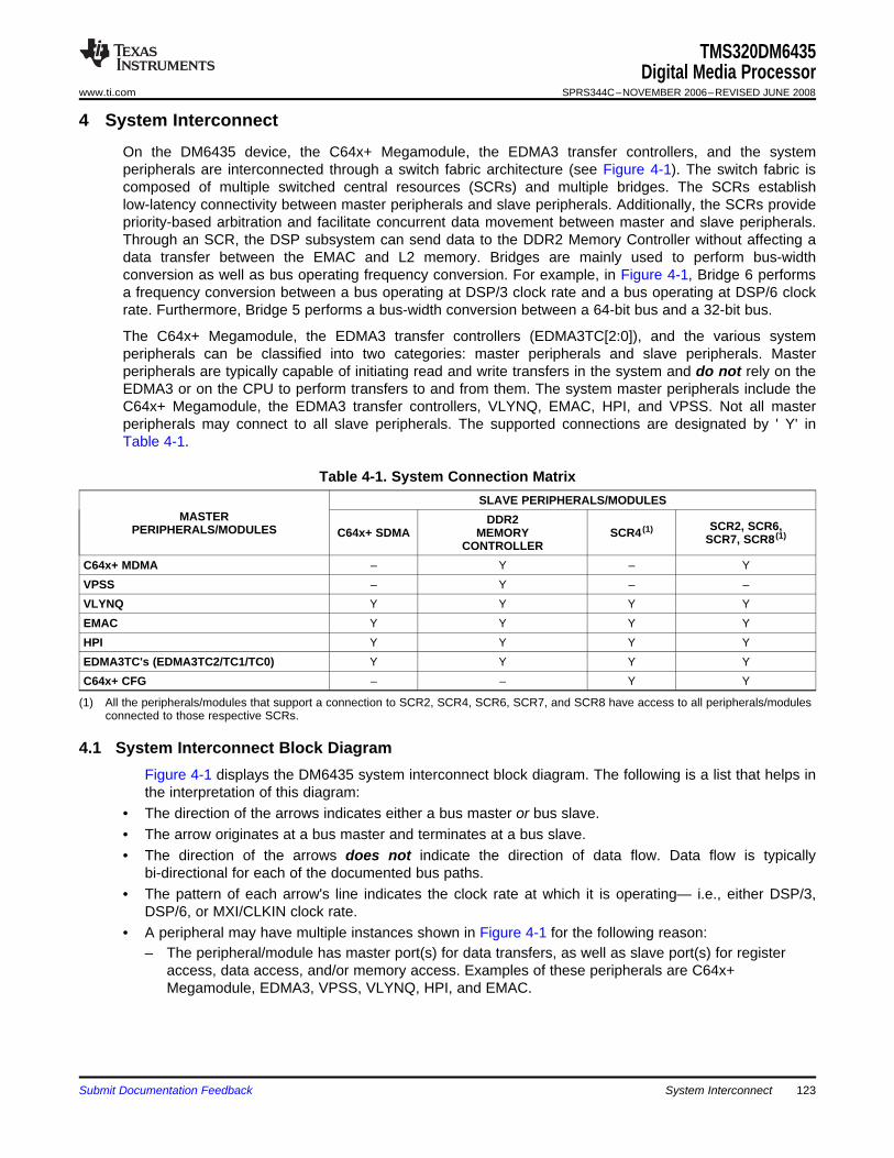
4 System Interconnect
4.1 System Interconnect Block Diagram
TMS320DM6435Digital Media Processor
www.ti.com SPRS344C–NOVEMBER 2006–REVISED JUNE 2008
On the DM6435 device, the C64x+ Megamodule, the EDMA3 transfer controllers, and the systemperipherals are interconnected through a switch fabric architecture (see Figure 4-1). The switch fabric iscomposed of multiple switched central resources (SCRs) and multiple bridges. The SCRs establishlow-latency connectivity between master peripherals and slave peripherals. Additionally, the SCRs providepriority-based arbitration and facilitate concurrent data movement between master and slave peripherals.Through an SCR, the DSP subsystem can send data to the DDR2 Memory Controller without affecting adata transfer between the EMAC and L2 memory. Bridges are mainly used to perform bus-widthconversion as well as bus operating frequency conversion. For example, in Figure 4-1, Bridge 6 performsa frequency conversion between a bus operating at DSP/3 clock rate and a bus operating at DSP/6 clockrate. Furthermore, Bridge 5 performs a bus-width conversion between a 64-bit bus and a 32-bit bus.
The C64x+ Megamodule, the EDMA3 transfer controllers (EDMA3TC[2:0]), and the various systemperipherals can be classified into two categories: master peripherals and slave peripherals. Masterperipherals are typically capable of initiating read and write transfers in the system and do not rely on theEDMA3 or on the CPU to perform transfers to and from them. The system master peripherals include theC64x+ Megamodule, the EDMA3 transfer controllers, VLYNQ, EMAC, HPI, and VPSS. Not all masterperipherals may connect to all slave peripherals. The supported connections are designated by ' Y' inTable 4-1.
Table 4-1. System Connection MatrixSLAVE PERIPHERALS/MODULES
MASTER DDR2 SCR2, SCR6,PERIPHERALS/MODULES C64x+ SDMA MEMORY SCR4 (1)SCR7, SCR8 (1)
CONTROLLERC64x+ MDMA – Y – YVPSS – Y – –VLYNQ Y Y Y YEMAC Y Y Y YHPI Y Y Y YEDMA3TC's (EDMA3TC2/TC1/TC0) Y Y Y YC64x+ CFG – – Y Y
(1) All the peripherals/modules that support a connection to SCR2, SCR4, SCR6, SCR7, and SCR8 have access to all peripherals/modulesconnected to those respective SCRs.
Figure 4-1 displays the DM6435 system interconnect block diagram. The following is a list that helps inthe interpretation of this diagram:
• The direction of the arrows indicates either a bus master or bus slave.• The arrow originates at a bus master and terminates at a bus slave.• The direction of the arrows does not indicate the direction of data flow. Data flow is typically
bi-directional for each of the documented bus paths.• The pattern of each arrow's line indicates the clock rate at which it is operating— i.e., either DSP/3,
DSP/6, or MXI/CLKIN clock rate.• A peripheral may have multiple instances shown in Figure 4-1 for the following reason:
– The peripheral/module has master port(s) for data transfers, as well as slave port(s) for registeraccess, data access, and/or memory access. Examples of these peripherals are C64x+Megamodule, EDMA3, VPSS, VLYNQ, HPI, and EMAC.
Submit Documentation Feedback System Interconnect 123

EMAC ControlModule Reg
EMAC ControlModule RAM
Bridge 8
SCR 3
SCR 1
VLYNQ
EMAC
HPI
VPSS
EDMA3TC0
EDMA3TC1
SCR 5 Bridge 2
L2 Cache
EDMA3TC0
EDMA3TC1
Read
Write
64
64
64
64
32
32
32
EDMA3CC
EDMA3TC2
Bridge 564
Bridge 464
Bridge 364
32
32
SCR 4
Bridge 6
32
32 32
32
32
32
EDMA3TC2
SCR 6
HPI
VPSS Reg
EMAC Reg
MDIO
GPIO
System Reg
PSC
PLLC1
PLLC2
SCR 2
UART0
UART1
HECC
I2C
PWM0
PWM1
PWM2
Timer0
Timer1
Timer2
SCR 7
EMIFA
VLYNQ
DSP/3 Clock Rate
DSP/6 Clock Rate
MXI/CLKIN Clock Rate
64x+L2/L1
SD
MA
DDR2 MemoryController
(Memory/Register)
Read
Write
64
64
Read
Write
64
64
64
64
64x+
MD
MA
CF
G
32
32
32
323232
32
32
32
32
32
32
32
32
32
32
32
32
32
32
32
32
32
32
32
32
32
64
DSP/6 Clock Rate
DSP/3 Clock Rate
DSP/6 Clock Rate
MXI/CLKIN Clock Rate
SCR 8
McBSP0
McASP0
32
32
32
TMS320DM6435Digital Media ProcessorSPRS344C–NOVEMBER 2006–REVISED JUNE 2008 www.ti.com
Figure 4-1. System Interconnect Block Diagram
System Interconnect124 Submit Documentation Feedback
5 Device Operating Conditions
5.1 Absolute Maximum Ratings Over Operating Temperature Range (Unless Otherwise
TMS320DM6435Digital Media Processor
www.ti.com SPRS344C–NOVEMBER 2006–REVISED JUNE 2008
Noted) (1)
Supply voltage ranges: Core (CVDD) (2) –0.5 V to 1.5 VI/O, 3.3V (DVDD33) (2) –0.5 V to 4.2 VI/O, 1.8V (DVDDR2, DDR_VDDDLL, PLLPWR18, MXVDD)(2) –0.5 to 2.5 V
Input voltage ranges: VI I/O, 3.3-V pins –0.5 V to 4.2 VVI I/O, 1.8 V –0.5 V to 2.5 V
Output voltage ranges: VO I/O, 3.3-V pins –0.5 V to 4.2 VVO I/O, 1.8 V –0.5 V to 2.5 V
Operating Junction temperature Commercial 0C to 90Cranges, TJ: Automotive –40C to 125C
(Q or S suffix)Storage temperature range, Tstg (default) –65C to 150C
(1) Stresses beyond those listed under "absolute maximum ratings" may cause permanent damage to the device. These are stress ratingsonly, and functional operation of the device at these or any other conditions beyond those indicated under "recommended operatingconditions" is not implied. Exposure to absolute-maximum-rated conditions for extended periods may affect device reliability.
(2) All voltage values are with respect to VSS.
Submit Documentation Feedback Device Operating Conditions 125
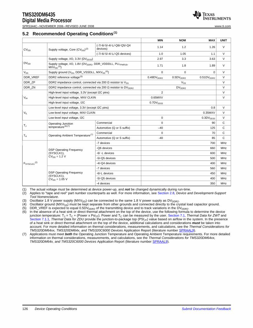
5.2 Recommended Operating Conditions (1)
TMS320DM6435Digital Media ProcessorSPRS344C–NOVEMBER 2006–REVISED JUNE 2008 www.ti.com
MIN NOM MAX UNIT
(-7/-6/-5/-4/-L/-Q6/-Q5/-Q4 1.14 1.2 1.26 Vdevices)CVDD Supply voltage, Core (CVDD) (2)
(-7/-6/-5/-4/-L/-Q5 devices) 1.0 1.05 1.1 V
Supply voltage, I/O, 3.3V (DVDD33) 2.97 3.3 3.63 VDVDD Supply voltage, I/O, 1.8V (DVDDR2, DDR_VDDDLL, PLLPWR18, 1.71 1.8 1.89 VMXVDD
(3))
VSS Supply ground (VSS, DDR_VSSDLL, MXVSS(4)) 0 0 0 V
DDR_VREF DDR2 reference voltage (5) 0.49DVDDR2 0.5DVDDR2 0.51DVDDR2 V
DDR_ZP DDR2 impedance control, connected via 200 Ω resistor to VSS VSS V
DDR_ZN DDR2 impedance control, connected via 200 Ω resistor to DVDDR2 DVDDR2 V
High-level input voltage, 3.3V (except I2C pins) 2 V
VIH High-level input voltage, MXI/ CLKIN 0.65MXV V
High-level input voltage, I2C 0.7DVDD33
Low-level input voltage, 3.3V (except I2C pins) 0.8 V
VIL Low-level input voltage, MXI/ CLKIN 0.35MXV V
Low-level input voltage, I2C 0 0.3DVDD33 V
Commercial 0 90 COperating JunctionTJ temperature (6) (7)Automotive (Q or S suffix) –40 125 C
Commercial 0 70 CTA Operating Ambient Temperature (7)
Automotive (Q or S suffix) -40 85 C
-7 devices 700 MHz
-Q6 devices 660 MHzDSP Operating Frequency(SYSCLK1), -6/ -L devices 600 MHzCVDD = 1.2 V -5/-Q5 devices 500 MHz
FSYSCLK1(2) -4/-Q4 devices 400 MHz
-7 devices 560 MHzDSP Operating Frequency -6/-L devices 450 MHz(SYSCLK1),
-5/-Q5 devices 400 MHzCVDD = 1.05 V-4 devices 350 MHz
(1) The actual voltage must be determined at device power-up, and not be changed dynamically during run-time.(2) Applies to "tape and reel" part number counterparts as well. For more information, see Section 2.8, Device and Development-Support
Tool Nomenclature.(3) Oscillator 1.8 V power supply (MXVDD) can be connected to the same 1.8 V power supply as DVDDR2.(4) Oscillator ground (MXVSS) must be kept separate from other grounds and connected directly to the crystal load capacitor ground.(5) DDR_VREF is expected to equal 0.5DVDDR2 of the transmitting device and to track variations in the DVDDR2.(6) In the absence of a heat sink or direct thermal attachment on the top of the device, use the following formula to determine the device
junction temperature: TJ = TC + (Power x PsiJT). Power and TC can be measured by the user. Section 7.1, Thermal Data for ZWT andSection 7.1.1, Thermal Data for ZDU provide the junction-to-package top (PSIJT) value based on airflow in the system. In the presenceof a heat sink or direct thermal attachment on the top of the device, additional calculations and considerations must be taken intoaccount. For more detailed information on thermal considerations, measurements, and calculations, see the Thermal Considerations forTMS320DM64xx, TMS320DM64x, and TMS320C6000 Devices Application Report (literature number SPRAAL9).
(7) Applications must meet both the Operating Junction Temperature and Operating Ambient Temperature requirements. For more detailedinformation on thermal considerations, measurements, and calculations, see the Thermal Considerations for TMS320DM64xx,TMS320DM64x, and TMS320C6000 Devices Application Report (literature number SPRAAL9).
Device Operating Conditions126 Submit Documentation Feedback
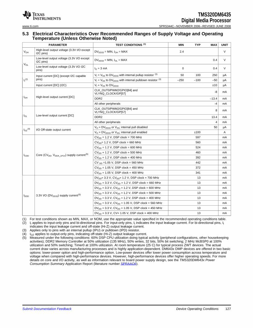
5.3 Electrical Characteristics Over Recommended Ranges of Supply Voltage and Operating
TMS320DM6435Digital Media Processor
www.ti.com SPRS344C–NOVEMBER 2006–REVISED JUNE 2008
Temperature (Unless Otherwise Noted)PARAMETER TEST CONDITIONS (1) MIN TYP MAX UNIT
High-level output voltage (3.3V I/O exceptVOH DVDD33 = MIN, IOH = MAX 2.4 VI2C pins)
Low-level output voltage (3.3V I/O except DVDD33 = MIN, IOL = MAX 0.4 VI2C pins)VOL
Low-level output voltage (3.3V I/O I2C IO = 3 mA 0 0.4 Vpins)
VI = VSS to DVDD33 with internal pullup resistor (3) 50 100 250 µAInput current [DC] (except I2C capablepins)II (2) VI = VSS to DVDD33 with internal pulldown resistor (3) –250 –100 –50 µA
Input current [DC] (I2C) VI = VSS to DVDD33 ±10 µA
CLK_OUT0/PWM2/GPIO[84] and -8 mAVLYNQ_CLOCK/GP[57]IOH High-level output current [DC] DDR2 –13.4 mA
All other peripherals -4 mA
CLK_OUT0/PWM2/GPIO[84] and 8 mAVLYNQ_CLOCK/GP[57]IOL Low-level output current [DC] DDR2 13.4 mA
All other peripherals 4 mA
VO = DVDD33 or VSS; internal pull disabled 50 µAIOZ
(4) I/O Off-state output currentVO = DVDD33 or VSS; internal pull enabled ±100 A
CVDD = 1.2 V, DSP clock = 700 MHz 597 mA
CVDD= 1.2 V, DSP clock = 660 MHz 560 mA
CVDD = 1.2 V, DSP clock = 600 MHz 524 mA
CVDD = 1.2 V, DSP clock = 500 MHz 460 mAICDD Core (CVDD, VDDA_1P1V) supply current (5)
CVDD = 1.2 V, DSP clock = 400 MHz 392 mA
CV DD =1.05 V, DSP clock = 560 MHz 442 mA
CVDD = 1.05 V, DSP clock = 450 MHz 372 mA
CVDD = 1.05 V, DSP clock = 400 MHz 341 mA
DVDD= 3.3 V, CVDD= 1.2 V, DSP clock = 700 MHz 13 mA
DVDD = 3.3 V, CVDD = 1.2 V, DSP clock = 660 MHz 13 mA
DVDD = 3.3 V, CVDD = 1.2 V, DSP clock = 600 MHz 13 mA
DVDD = 3.3 V, CVDD = 1.2 V, DSP clock = 500 MHz 13 mAIDDD 3.3V I/O (DVDD33) supply current(5)
DVDD = 3.3 V, CVDD = 1.2 V, DSP clock = 400 MHz 13 mA
DVDD = 3.3 V, CVDD = 1.05 V, DSP clock = 560 MHz 13 mA
DVDD = 3.3 V, CVDD = 1.05 V, DSP clock = 450 MHz 13 mA
DVDD = 3.3 V, CV= 1.05 V, DSP clock = 400 MHz 13 mA
(1) For test conditions shown as MIN, MAX, or NOM, use the appropriate value specified in the recommended operating conditions table.(2) II applies to input-only pins and bi-directional pins. For input-only pins, II indicates the input leakage current. For bi-directional pins, II
indicates the input leakage current and off-state (Hi-Z) output leakage current.(3) Applies only to pins with an internal pullup (IPU) or pulldown (IPD) resistor.(4) IOZ applies to output-only pins, indicating off-state (Hi-Z) output leakage current.(5) Measured under the following conditions: 60% DSP CPU utilization doing typical activity (peripheral configurations, other housekeeping
activities); DDR2 Memory Controller at 50% utilization (135 MHz), 50% writes, 32 bits, 50% bit switching; 2 MHz McBSP0 at 100%utilization and 50% switching; Timer0 at 100% utilization. At room temperature (25 C) for typical process ZWT devices. The actualcurrent draw varies across manufacturing processes and is highly application-dependent. DM643x DMP devices are offered in two basicoptions: lower-power option and high-performance option. Low-power devices offer lower power consumption across temperature andvoltage when compared with high-performance devices. However, high-performance devices offer higher operating speeds. For moredetails on core and I/O activity, as well as information relevant to board power supply design, see the TMS320DM643x PowerConsumption Summary Application Report (literature number SPRAAO6).
Submit Documentation Feedback Device Operating Conditions 127
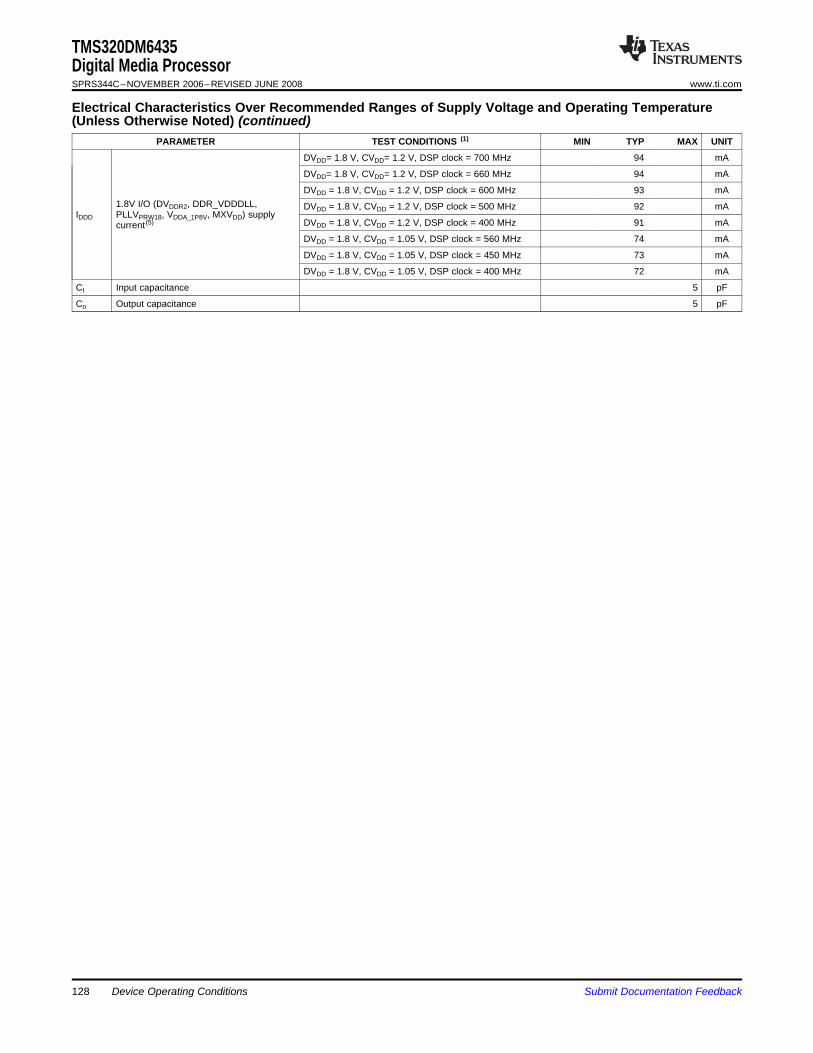
TMS320DM6435Digital Media ProcessorSPRS344C–NOVEMBER 2006–REVISED JUNE 2008 www.ti.com
Electrical Characteristics Over Recommended Ranges of Supply Voltage and Operating Temperature(Unless Otherwise Noted) (continued)
PARAMETER TEST CONDITIONS (1) MIN TYP MAX UNIT
DVDD= 1.8 V, CVDD= 1.2 V, DSP clock = 700 MHz 94 mA
DVDD= 1.8 V, CVDD= 1.2 V, DSP clock = 660 MHz 94 mA
DVDD = 1.8 V, CVDD = 1.2 V, DSP clock = 600 MHz 93 mA1.8V I/O (DVDDR2, DDR_VDDDLL, DVDD = 1.8 V, CVDD = 1.2 V, DSP clock = 500 MHz 92 mA
IDDD PLLVPRW18, VDDA_1P8V, MXVDD) supplyDVDD = 1.8 V, CVDD = 1.2 V, DSP clock = 400 MHz 91 mAcurrent (5)
DVDD = 1.8 V, CVDD = 1.05 V, DSP clock = 560 MHz 74 mA
DVDD = 1.8 V, CVDD = 1.05 V, DSP clock = 450 MHz 73 mA
DVDD = 1.8 V, CVDD = 1.05 V, DSP clock = 400 MHz 72 mA
CI Input capacitance 5 pF
Co Output capacitance 5 pF
128 Device Operating Conditions Submit Documentation Feedback
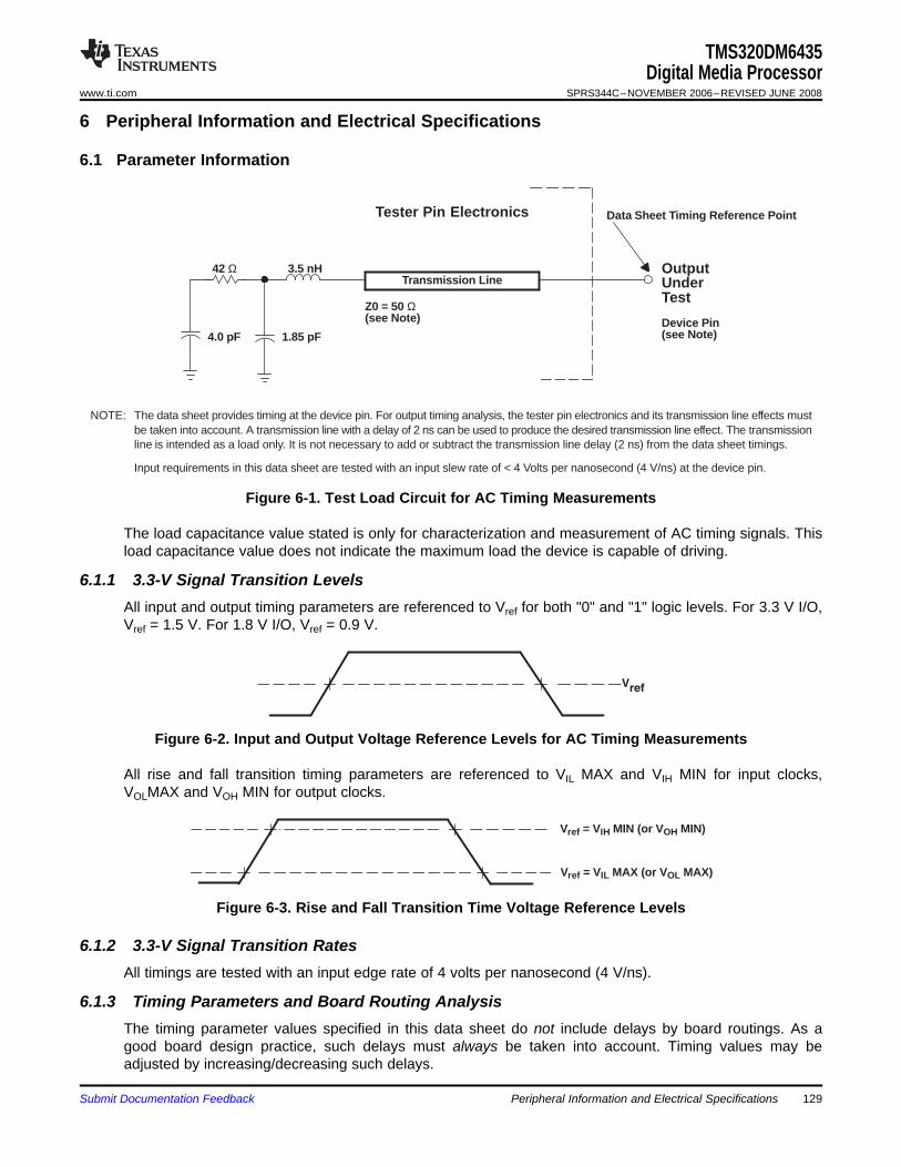
6 Peripheral Information and Electrical Specifications
6.1 Parameter Information
Transmission Line
4.0 pF 1.85 pF
Z0 = 50 Ω(see Note)
Tester Pin Electronics Data Sheet Timing Reference Point
OutputUnderTest
NOTE: The data sheet provides timing at the device pin. For output timing analysis, the tester pin electronics and its transmission line effects mustbe taken into account. A transmission line with a delay of 2 ns can be used to produce the desired transmission line effect. The transmissionline is intended as a load only. It is not necessary to add or subtract the transmission line delay (2 ns) from the data sheet timings.
Input requirements in this data sheet are tested with an input slew rate of < 4 Volts per nanosecond (4 V/ns) at the device pin.
42 Ω 3.5 nH
Device Pin(see Note)
6.1.1 3.3-V Signal Transition Levels
Vref
Vref = VIL MAX (or VOL MAX)
Vref = VIH MIN (or VOH MIN)
6.1.2 3.3-V Signal Transition Rates
6.1.3 Timing Parameters and Board Routing Analysis
TMS320DM6435Digital Media Processor
www.ti.com SPRS344C–NOVEMBER 2006–REVISED JUNE 2008
Figure 6-1. Test Load Circuit for AC Timing Measurements
The load capacitance value stated is only for characterization and measurement of AC timing signals. Thisload capacitance value does not indicate the maximum load the device is capable of driving.
All input and output timing parameters are referenced to Vref for both "0" and "1" logic levels. For 3.3 V I/O,Vref = 1.5 V. For 1.8 V I/O, Vref = 0.9 V.
Figure 6-2. Input and Output Voltage Reference Levels for AC Timing Measurements
All rise and fall transition timing parameters are referenced to VIL MAX and VIH MIN for input clocks,VOLMAX and VOH MIN for output clocks.
Figure 6-3. Rise and Fall Transition Time Voltage Reference Levels
All timings are tested with an input edge rate of 4 volts per nanosecond (4 V/ns).
The timing parameter values specified in this data sheet do not include delays by board routings. As agood board design practice, such delays must always be taken into account. Timing values may beadjusted by increasing/decreasing such delays.
Submit Documentation Feedback Peripheral Information and Electrical Specifications 129
6.2 Recommended Clock and Control Signal Transition Behavior
6.3 Power Supplies
6.3.1 Power-Supply Sequencing
6.3.2 Power-Supply Design Considerations
6.3.3 Power-Supply Decoupling
TMS320DM6435Digital Media ProcessorSPRS344C–NOVEMBER 2006–REVISED JUNE 2008 www.ti.com
TI recommends utilizing the available I/O buffer information specification (IBIS) models to analyze thetiming characteristics correctly. To properly use IBIS models to attain accurate timing analysis for a givensystem, see the Using IBIS Models for Timing Analysis application report (literature number SPRA839). Ifneeded, external logic hardware such as buffers may be used to compensate any timing differences.
For the DDR2 memory controller interface, it is not necessary to use the IBIS models to analyze timingcharacteristics. TI provides a PCB routing rules solution that describes the routing rules to ensure theDDR2 memory controller interface timings are met. See the Implementing DDR2 PCB Layout on theTMS320DM643x DMP DMSoC Application Report (literature number SPRAAL6).
All clocks and control signals must transition between VIH and VIL (or between VIL and VIH) in a monotonicmanner.
For more information regarding TI's power management products and suggested devices to power TIDSPs, visit www.ti.com/dsppower.
The DM6435 includes one core supply (CVDD), and two I/O supplies—DVDD33 and DVDDR2. To ensureproper device operation, a specific power-up sequence must be followed. Some TI power-supply devicesinclude features that facilitate power sequencing—for example, Auto-Track and Slow-Start/Enablefeatures. For more information on TI power supplies and their features, visit www.ti.com/dsppower.
Here is a summary of the power sequencing requirements:• The power ramp order must be DVDD33 before DVDDR2, and DVDDR2 before CVDD—meaning during
power up, the voltage at the DVDDR2 rail should never exceed the voltage at the DVDD33 rail. Similarly,the voltage at the CVDD rail should never exceed the voltage at the DVDDR2 rail.
• From the time that power ramp begins, all power supplies (DVDD33, DVDDR2, CVDD) must be stablewithin 200 ms. The term "stable" means reaching the recommended operating condition (seeSection 5.2, Recommended Operating Conditions table).
Core and I/O supply voltage regulators should be located close to the DSP to minimize inductance andresistance in the power delivery path. Additionally, when designing for high-performance applicationsutilizing the DM6435 device, the PC board should include separate power planes for core, I/O, andground; all bypassed with high-quality low-ESL/ESR capacitors.
In order to properly decouple the supply planes from system noise, place as many capacitors (caps) aspossible close to the DSP. These caps need to be close to the DSP, no more than 1.25 cm maximumdistance to be effective. Physically smaller caps are better, such as 0402, but need to be evaluated from ayield/manufacturing point-of-view. Parasitic inductance limits the effectiveness of the decouplingcapacitors, therefore physically smaller capacitors should be used while maintaining the largest availablecapacitance value.
Larger caps for each supply can be placed further away for bulk decoupling. Large bulk caps (on the orderof 100 µF) should be furthest away, but still as close as possible. Large caps for each supply should beplaced outside of the BGA footprint.
As with the selection of any component, verification of capacitor availability over the product's productionlifetime should be considered.
For more details on capacitor usage and placement, see the Implementing DDR2 PCB Layout on theTMS320DM643x DMP DMSoC Application Report (literature number SPRAAL6).
Peripheral Information and Electrical Specifications130 Submit Documentation Feedback
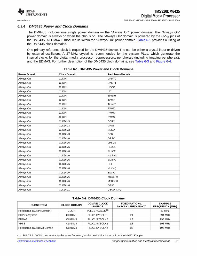
6.3.4 DM6435 Power and Clock Domains
TMS320DM6435Digital Media Processor
www.ti.com SPRS344C–NOVEMBER 2006–REVISED JUNE 2008
The DM6435 includes one single power domain — the "Always On" power domain. The "Always On"power domain is always on when the chip is on. The "Always On" domain is powered by the CVDD pins ofthe DM6435. All DM6435 modules lie within the "Always On" power domain. Table 6-1 provides a listing ofthe DM6435 clock domains.
One primary reference clock is required for the DM6435 device. The can be either a crystal input or drivenby external oscillators. A 27-MHz crystal is recommended for the system PLLs, which generate theinternal clocks for the digital media processor, coprocessors, peripherals (including imaging peripherals),and the EDMA3. For further description of the DM6435 clock domains, see Table 6-3 and Figure 6-4.
Table 6-1. DM6435 Power and Clock DomainsPower Domain Clock Domain Peripheral/ModuleAlways On CLKIN UART0Always On CLKIN UART1Always On CLKIN HECCAlways On CLKIN I2CAlways On CLKIN Timer0Always On CLKIN Timer1Always On CLKIN Timer2Always On CLKIN PWM0Always On CLKIN PWM1Always On CLKIN PWM2Always On CLKDIV3 DDR2Always On CLKDIV3 VPSSAlways On CLKDIV3 EDMAAlways On CLKDIV3 SCRAlways On CLKDIV6 GPSCAlways On CLKDIV6 LPSCsAlways On CLKDIV6 PLLC1Always On CLKDIV6 PLLC2Always On CLKDIV6 Ice PickAlways On CLKDIV6 EMIFAAlways On CLKDIV6 HPIAlways On CLKDIV6 VLYNQAlways On CLKDIV6 EMACAlways On CLKDIV6 McASP0Always On CLKDIV6 McBSP0Always On CLKDIV6 GPIOAlways On CLKDIV1 C64x+ CPU
Table 6-2. DM6435 Clock DomainsDOMAIN CLOCK FIXED RATIO vs. EXAMPLESUBSYSTEM CLOCK DOMAIN SOURCE SYSCLK1 FREQUENCY FREQUENCY (MHz)
Peripherals (CLKIN Domain) CLKIN PLLC1 AUXCLK (1) – 27 MHzDSP Subsystem CLKDIV1 PLLC1 SYSCLK1 1:1 594 MHzEDMA3 CLKDIV3 PLLC1 SYSCLK2 1:3 198 MHzVPSS CLKDIV3 PLLC1 SYSCLK2 1:3 198 MHzPeripherals (CLKDIV3 Domain) CLKDIV3 PLLC1 SYSCLK2 1:3 198 MHz
(1) PLLC1 AUXCLK runs at exactly the same frequency as the device clock source from the MXI/CLKIN pin.
Submit Documentation Feedback Peripheral Information and Electrical Specifications 131
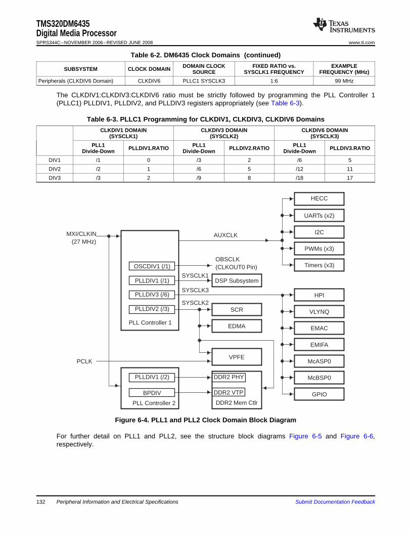
DSP SubsystemSYSCLK1
SYSCLK3
SCR
EDMA
VPFE
DDR2 PHY
DDR2 VTP
DDR2 Mem Ctlr
PLLDIV1 (/2)
BPDIV
PLL Controller 2
PLL Controller 1
PLLDIV2 (/3)
PLLDIV3 (/6)
PLLDIV1 (/1)
SYSCLK2
UARTs (x2)
I2C
Timers (x3)
PWMs (x3)
EMAC
EMIFA
VLYNQ
HPI
McASP0
McBSP0
GPIO
MXI/CLKIN(27 MHz)
PCLK
OSCDIV1 (/1)
HECC
OBSCLK(CLKOUT0 Pin)
AUXCLK
TMS320DM6435Digital Media ProcessorSPRS344C–NOVEMBER 2006–REVISED JUNE 2008 www.ti.com
Table 6-2. DM6435 Clock Domains (continued)DOMAIN CLOCK FIXED RATIO vs. EXAMPLESUBSYSTEM CLOCK DOMAIN SOURCE SYSCLK1 FREQUENCY FREQUENCY (MHz)
Peripherals (CLKDIV6 Domain) CLKDIV6 PLLC1 SYSCLK3 1:6 99 MHz
The CLKDIV1:CLKDIV3:CLKDIV6 ratio must be strictly followed by programming the PLL Controller 1(PLLC1) PLLDIV1, PLLDIV2, and PLLDIV3 registers appropriately (see Table 6-3).
Table 6-3. PLLC1 Programming for CLKDIV1, CLKDIV3, CLKDIV6 DomainsCLKDIV1 DOMAIN CLKDIV3 DOMAIN CLKDIV6 DOMAIN
(SYSCLK1) (SYSCLK2) (SYSCLK3)PLL1 PLL1 PLL1PLLDIV1.RATIO PLLDIV2.RATIO PLLDIV3.RATIODivide-Down Divide-Down Divide-Down
DIV1 /1 0 /3 2 /6 5DIV2 /2 1 /6 5 /12 11DIV3 /3 2 /9 8 /18 17
Figure 6-4. PLL1 and PLL2 Clock Domain Block Diagram
For further detail on PLL1 and PLL2, see the structure block diagrams Figure 6-5 and Figure 6-6,respectively.
Peripheral Information and Electrical Specifications132 Submit Documentation Feedback
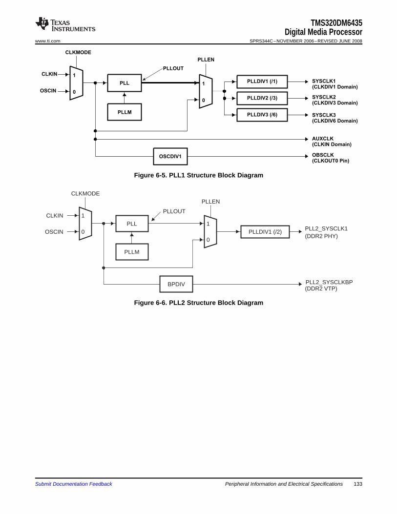
PLLDIV1 (/1)
PLLDIV3 (/6)
PLLDIV2 (/3)
SYSCLK1(CLKDIV1 Domain)
SYSCLK3(CLKDIV6 Domain)
SYSCLK2(CLKDIV3 Domain)
1
0
PLLM
PLL
0
1
CLKMODE
CLKIN
OSCIN
PLLEN
AUXCLK(CLKIN Domain)
OSCDIV1 OBSCLK(CLKOUT0 Pin)
PLLOUT
PLLDIV1 (/2)1
0
PLLM
PLL0
1
BPDIV
CLKMODE
CLKIN
OSCIN
PLLEN
PLL2_SYSCLK1(DDR2 PHY)
PLL2_SYSCLKBP(DDR2 VTP)
PLLOUT
TMS320DM6435Digital Media Processor
www.ti.com SPRS344C–NOVEMBER 2006–REVISED JUNE 2008
Figure 6-5. PLL1 Structure Block Diagram
Figure 6-6. PLL2 Structure Block Diagram
Submit Documentation Feedback Peripheral Information and Electrical Specifications 133
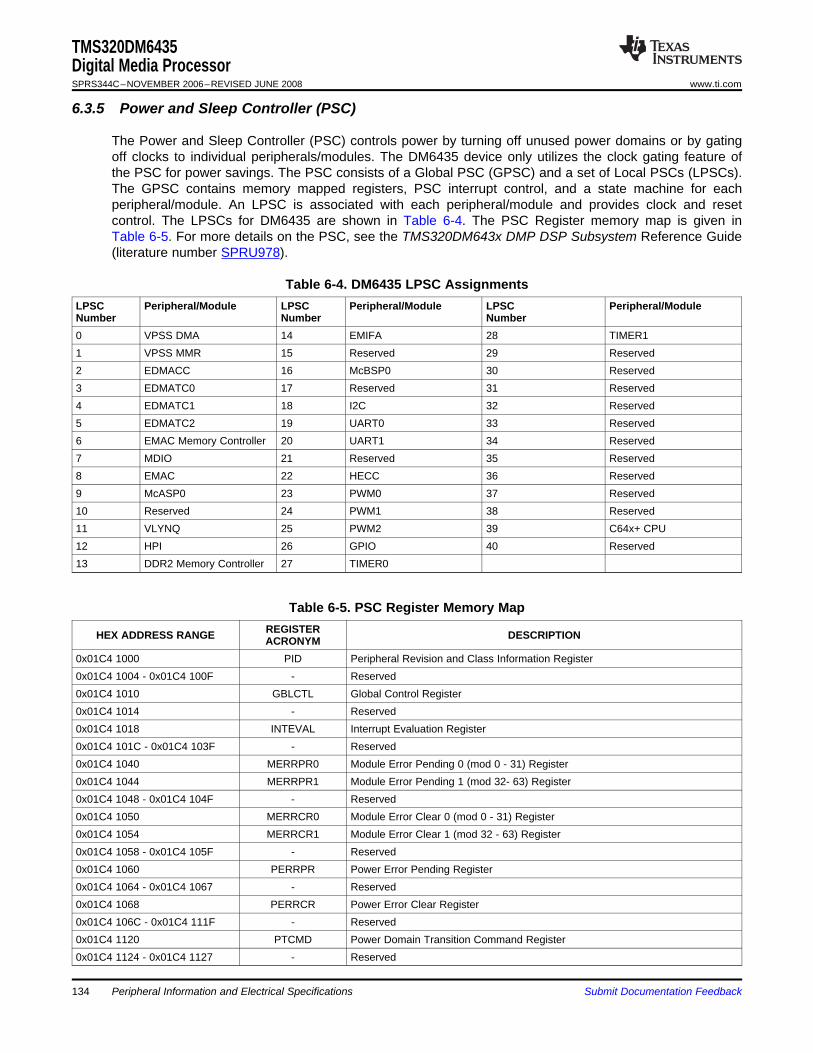
6.3.5 Power and Sleep Controller (PSC)
TMS320DM6435Digital Media ProcessorSPRS344C–NOVEMBER 2006–REVISED JUNE 2008 www.ti.com
The Power and Sleep Controller (PSC) controls power by turning off unused power domains or by gatingoff clocks to individual peripherals/modules. The DM6435 device only utilizes the clock gating feature ofthe PSC for power savings. The PSC consists of a Global PSC (GPSC) and a set of Local PSCs (LPSCs).The GPSC contains memory mapped registers, PSC interrupt control, and a state machine for eachperipheral/module. An LPSC is associated with each peripheral/module and provides clock and resetcontrol. The LPSCs for DM6435 are shown in Table 6-4. The PSC Register memory map is given inTable 6-5. For more details on the PSC, see the TMS320DM643x DMP DSP Subsystem Reference Guide(literature number SPRU978).
Table 6-4. DM6435 LPSC AssignmentsLPSC Peripheral/Module LPSC Peripheral/Module LPSC Peripheral/ModuleNumber Number Number0 VPSS DMA 14 EMIFA 28 TIMER11 VPSS MMR 15 Reserved 29 Reserved2 EDMACC 16 McBSP0 30 Reserved3 EDMATC0 17 Reserved 31 Reserved4 EDMATC1 18 I2C 32 Reserved5 EDMATC2 19 UART0 33 Reserved6 EMAC Memory Controller 20 UART1 34 Reserved7 MDIO 21 Reserved 35 Reserved8 EMAC 22 HECC 36 Reserved9 McASP0 23 PWM0 37 Reserved10 Reserved 24 PWM1 38 Reserved11 VLYNQ 25 PWM2 39 C64x+ CPU12 HPI 26 GPIO 40 Reserved13 DDR2 Memory Controller 27 TIMER0
Table 6-5. PSC Register Memory MapREGISTERHEX ADDRESS RANGE DESCRIPTIONACRONYM
0x01C4 1000 PID Peripheral Revision and Class Information Register0x01C4 1004 - 0x01C4 100F - Reserved0x01C4 1010 GBLCTL Global Control Register0x01C4 1014 - Reserved0x01C4 1018 INTEVAL Interrupt Evaluation Register0x01C4 101C - 0x01C4 103F - Reserved0x01C4 1040 MERRPR0 Module Error Pending 0 (mod 0 - 31) Register0x01C4 1044 MERRPR1 Module Error Pending 1 (mod 32- 63) Register0x01C4 1048 - 0x01C4 104F - Reserved0x01C4 1050 MERRCR0 Module Error Clear 0 (mod 0 - 31) Register0x01C4 1054 MERRCR1 Module Error Clear 1 (mod 32 - 63) Register0x01C4 1058 - 0x01C4 105F - Reserved0x01C4 1060 PERRPR Power Error Pending Register0x01C4 1064 - 0x01C4 1067 - Reserved0x01C4 1068 PERRCR Power Error Clear Register0x01C4 106C - 0x01C4 111F - Reserved0x01C4 1120 PTCMD Power Domain Transition Command Register0x01C4 1124 - 0x01C4 1127 - Reserved
Peripheral Information and Electrical Specifications134 Submit Documentation Feedback
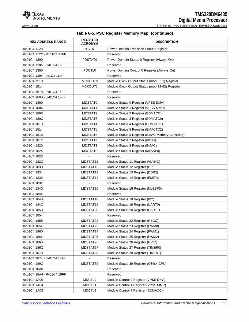
TMS320DM6435Digital Media Processor
www.ti.com SPRS344C–NOVEMBER 2006–REVISED JUNE 2008
Table 6-5. PSC Register Memory Map (continued)REGISTERHEX ADDRESS RANGE DESCRIPTIONACRONYM
0x01C4 1128 PTSTAT Power Domain Transition Status Register0x01C4 112C - 0x01C4 11FF - Reserved0x01C4 1200 PDSTAT0 Power Domain Status 0 Register (Always On)0x01C4 1204 - 0x01C4 12FF - Reserved0x01C4 1300 PDCTL0 Power Domain Control 0 Register (Always On)0x01C4 1304 - 0x1C4 150F - Reserved0x01C4 1510 MCKOUT0 Module Clock Output Status (mod 0-31) Register0x01C4 1514 MCKOUT1 Module Clock Output Status (mod 32-63) Register0x01C4 1518 - 0x01C4 15FF - Reserved0x01C4 1600 - 0x01C4 17FF - Reserved0x01C4 1800 MDSTAT0 Module Status 0 Register (VPSS DMA)0x01C4 1804 MDSTAT1 Module Status 1 Register (VPSS MMR)0x01C4 1808 MDSTAT2 Module Status 2 Register (EDMACC)0x01C4 180C MDSTAT3 Module Status 3 Register (EDMATC0)0x01C4 1810 MDSTAT4 Module Status 4 Register (EDMATC1)0x01C4 1814 MDSTAT5 Module Status 5 Register (EMACTC2)0x01C4 1818 MDSTAT6 Module Status 6 Register (EMAC Memory Controller)0x01C4 181C MDSTAT7 Module Status 7 Register (MDIO)0x01C4 1820 MDSTAT8 Module Status 8 Register (EMAC)0x01C4 1824 MDSTAT9 Module Status 9 Register (McASP0)0x01C4 1828 - Reserved0x01C4 182C MDSTAT11 Module Status 11 Register (VLYNQ)0x01C4 1830 MDSTAT12 Module Status 12 Register (HPI)0x01C4 1834 MDSTAT13 Module Status 13 Register (DDR2)0x01C4 1838 MDSTAT14 Module Status 14 Register (EMIFA)0x01C4 183C - Reserved0x01C4 1840 MDSTAT16 Module Status 16 Register (McBSP0)0x01C4 1844 - Reserved0x01C4 1848 MDSTAT18 Module Status 18 Register (I2C)0x01C4 184C MDSTAT19 Module Status 19 Register (UART0)0x01C4 1850 MDSTAT20 Module Status 20 Register (UART1)0x01C4 1854 - Reserved0x01C4 1858 MDSTAT22 Module Status 22 Register (HECC)0x01C4 185C MDSTAT23 Module Status 23 Register (PWM0)0x01C4 1860 MDSTAT24 Module Status 24 Register (PWM1)0x01C4 1864 MDSTAT25 Module Status 25 Register (PWM2)0x01C4 1868 MDSTAT26 Module Status 26 Register (GPIO)0x01C4 186C MDSTAT27 Module Status 27 Register (TIMER0)0x01C4 1870 MDSTAT28 Module Status 28 Register (TIMER1)0x01C4 1874 - 0x01C4 189B - Reserved0x01C4 189C MDSTAT39 Module Status 39 Register (C64x+ CPU)0x01C4 18A0 - Reserved0x01C4 18A4 - 0x01C4 19FF - Reserved0x01C4 1A00 MDCTL0 Module Control 0 Register (VPSS DMA)0x01C4 1A04 MDCTL1 Module Control 1 Register (VPSS MMR)0x01C4 1A08 MDCTL2 Module Control 2 Register (EDMACC)
Submit Documentation Feedback Peripheral Information and Electrical Specifications 135
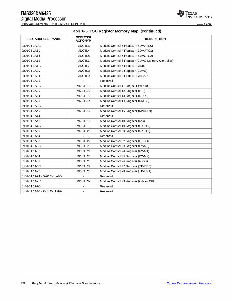
TMS320DM6435Digital Media ProcessorSPRS344C–NOVEMBER 2006–REVISED JUNE 2008 www.ti.com
Table 6-5. PSC Register Memory Map (continued)REGISTERHEX ADDRESS RANGE DESCRIPTIONACRONYM
0x01C4 1A0C MDCTL3 Module Control 3 Register (EDMATC0)0x01C4 1A10 MDCTL4 Module Control 4 Register (EDMATC1)0x01C4 1A14 MDCTL5 Module Control 5 Register (EMACTC2)0x01C4 1A18 MDCTL6 Module Control 6 Register (EMAC Memory Controller)0x01C4 1A1C MDCTL7 Module Control 7 Register (MDIO)0x01C4 1A20 MDCTL8 Module Control 8 Register (EMAC)0x01C4 1A24 MDCTL9 Module Control 9 Register (McASP0)0x01C4 1A28 - Reserved0x01C4 1A2C MDCTL11 Module Control 11 Register (VLYNQ)0x01C4 1A30 MDCTL12 Module Control 12 Register (HPI)0x01C4 1A34 MDCTL13 Module Control 13 Register (DDR2)0x01C4 1A38 MDCTL14 Module Control 14 Register (EMIFA)0x01C4 1A3C - Reserved0x01C4 1A40 MDCTL16 Module Control 16 Register (McBSP0)0x01C4 1A44 - Reserved0x01C4 1A48 MDCTL18 Module Control 18 Register (I2C)0x01C4 1A4C MDCTL19 Module Control 19 Register (UART0)0x01C4 1A50 MDCTL20 Module Control 20 Register (UART1)0x01C4 1A54 - Reserved0x01C4 1A58 MDCTL22 Module Control 22 Register (HECC)0x01C4 1A5C MDCTL23 Module Control 23 Register (PWM0)0x01C4 1A60 MDCTL24 Module Control 24 Register (PWM1)0x01C4 1A64 MDCTL25 Module Control 25 Register (PWM2)0x01C4 1A68 MDCTL26 Module Control 26 Register (GPIO)0x01C4 1A6C MDCTL27 Module Control 27 Register (TIMER0)0x01C4 1A70 MDCTL28 Module Control 28 Register (TIMER1)0x01C4 1A74 - 0x01C4 1A9B - Reserved0x01C4 1A9C MDCTL39 Module Control 39 Register (C64x+ CPU)0x01C4 1AA0 - Reserved0x01C4 1AA4 - 0x01C4 1FFF - Reserved
Peripheral Information and Electrical Specifications136 Submit Documentation Feedback
6.4 Enhanced Direct Memory Access (EDMA3) Controller
6.4.1 EDMA3 Channel Synchronization Events
TMS320DM6435Digital Media Processor
www.ti.com SPRS344C–NOVEMBER 2006–REVISED JUNE 2008
The EDMA controller handles all data transfers between memories and the device slave peripherals onthe DM6435 device. These data transfers include cache servicing, non-cacheable memory accesses,user-programmed data transfers, and host accesses. These are summarized as follows:• Transfer to/from on-chip memories
– DSP L1D memory– DSP L2 memory
• Transfer to/from external storage– DDR2 SDRAM– NAND flash– Asynchronous EMIF (EMIFA)
• Transfer to/from peripherals/hosts– VLYNQ– HPI– McBSP0– McASP0– PWM– UART0/1– HECC
The EDMA supports two addressing modes: constant addressing and increment addressing. On theDM6435, constant addressing mode is not supported by any peripheral or internal memory. For moreinformation on these two addressing modes, see the TMS320DM643x DMP Enhanced Direct MemoryAccess (EDMA3) Controller User’s Guide (literature number SPRU987).
The EDMA supports up to 64 EDMA channels which service peripheral devices and external memory.Table 6-6 lists the source of EDMA synchronization events associated with each of the programmableEDMA channels. For the DM6435 device, the association of an event to a channel is fixed; each of theEDMA channels has one specific event associated with it. These specific events are captured in theEDMA event registers (ER, ERH) even if the events are disabled by the EDMA event enable registers(EER, EERH). For more detailed information on the EDMA module and how EDMA events are enabled,captured, processed, linked, chained, and cleared, etc., see the TMS320DM643x DMP Enhanced DirectMemory Access (EDMA3) Controller User’s Guide (literature number SPRU987).
Table 6-6. DM6435 EDMA Channel Synchronization Events (1)
EDMA EVENT NAME EVENT DESCRIPTIONCHANNEL0-1 – Reserved2 XEVT0 McBSP0 Transmit Event3 REVT0 McBSP0 Receive Event4 – Reserved5 – Reserved6 HISTEVT VPSS Histogram Event7 H3AEVT VPSS H3A Event8 PRVUEVT VPSS Previewer Event9 RSZEVT VPSS Resizer Event
10 AXEVTE0 McASP0 Transmit Event Even
(1) In addition to the events shown in this table, each of the 64 channels can also be synchronized with the transfer completion or alternatetransfer completion events. For more detailed information on EDMA event-transfer chaining, see the Document Support section for theEnhanced Direct Memory Access (EDMA) Controller Reference Guide.
Submit Documentation Feedback Peripheral Information and Electrical Specifications 137
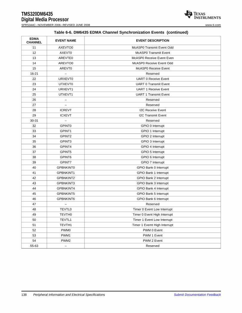
TMS320DM6435Digital Media ProcessorSPRS344C–NOVEMBER 2006–REVISED JUNE 2008 www.ti.com
Table 6-6. DM6435 EDMA Channel Synchronization Events (continued)EDMA EVENT NAME EVENT DESCRIPTIONCHANNEL
11 AXEVTO0 McASP0 Transmit Event Odd12 AXEVT0 McASP0 Transmit Event13 AREVTE0 McASP0 Receive Event Even14 AREVTO0 McASP0 Receive Event Odd15 AREVT0 McASP0 Receive Event
16-21 – Reserved22 URXEVT0 UART 0 Receive Event23 UTXEVT0 UART 0 Transmit Event24 URXEVT1 UART 1 Receive Event25 UTXEVT1 UART 1 Transmit Event26 – Reserved27 – Reserved28 ICREVT I2C Receive Event29 ICXEVT I2C Transmit Event
30-31 – Reserved32 GPINT0 GPIO 0 Interrupt33 GPINT1 GPIO 1 Interrupt34 GPINT2 GPIO 2 Interrupt35 GPINT3 GPIO 3 Interrupt36 GPINT4 GPIO 4 Interrupt37 GPINT5 GPIO 5 Interrupt38 GPINT6 GPIO 6 Interrupt39 GPINT7 GPIO 7 Interrupt40 GPBNKINT0 GPIO Bank 0 Interrupt41 GPBNKINT1 GPIO Bank 1 Interrupt42 GPBNKINT2 GPIO Bank 2 Interrupt43 GPBNKINT3 GPIO Bank 3 Interrupt44 GPBNKINT4 GPIO Bank 4 Interrupt45 GPBNKINT5 GPIO Bank 5 Interrupt46 GPBNKINT6 GPIO Bank 6 Interrupt47 – Reserved48 TEVTL0 Timer 0 Event Low Interrupt49 TEVTH0 Timer 0 Event High Interrupt50 TEVTL1 Timer 1 Event Low Interrupt51 TEVTH1 Timer 1 Evemt High Interrupt52 PWM0 PWM 0 Event53 PWM1 PWM 1 Event54 PWM2 PWM 2 Event
55-63 – Reserved
Peripheral Information and Electrical Specifications138 Submit Documentation Feedback

6.4.2 EDMA Peripheral Register Description(s)
TMS320DM6435Digital Media Processor
www.ti.com SPRS344C–NOVEMBER 2006–REVISED JUNE 2008
Table 6-7 lists the EDMA registers, their corresponding acronyms, and DM6435 device memory locations.
Table 6-7. DM6435 EDMA RegistersHEX ADDRESS ACRONYM REGISTER NAME
Channel Controller Registers0x01C0 0000 - 0x01C0 0003 Reserved
0x01C0 0004 CCCFG EDMA3CC Configuration Register0x01C0 0008 - 0x01C0 01FF Reserved
Global Registers0x01C0 0200 QCHMAP0 QDMA Channel 0 Mapping to PaRAM Register0x01C0 0204 QCHMAP1 QDMA Channel 1 Mapping to PaRAM Register0x01C0 0208 QCHMAP2 QDMA Channel 2 Mapping to PaRAM Register0x01C0 020C QCHMAP3 QDMA Channel 3 Mapping to PaRAM Register0x01C0 0210 QCHMAP4 QDMA Channel 4 Mapping to PaRAM Register0x01C0 0214 QCHMAP5 QDMA Channel 5 Mapping to PaRAM Register0x01C0 0218 QCHMAP6 QDMA Channel 6 Mapping to PaRAM Register0x01C0 021C QCHMAP7 QDMA Channel 7 Mapping to PaRAM Register0x01C0 0240 DMAQNUM0 DMA Queue Number Register 0 (Channels 00 to 07)0x01C0 0244 DMAQNUM1 DMA Queue Number Register 1 (Channels 08 to 15)0x01C0 0248 DMAQNUM2 DMA Queue Number Register 2 (Channels 16 to 23)0x01C0 024C DMAQNUM3 DMA Queue Number Register 3 (Channels 24 to 31)0x01C0 0250 DMAQNUM4 DMA Queue Number Register 4 (Channels 32 to 39)0x01C0 0254 DMAQNUM5 DMA Queue Number Register 5 (Channels 40 to 47)0x01C0 0258 DMAQNUM6 DMA Queue Number Register 6 (Channels 48 to 55)0x01C0 025C DMAQNUM7 DMA Queue Number Register 7 (Channels 56 to 63)0x01C0 0260 QDMAQNUM CC QDMA Queue Number
0x01C0 0264 - 0x01C0 0283 – Reserved0x01C0 0284 QUEPRI Queue Priority Register
0x01C0 0288 - 0x01C0 02FF – Reserved0x01C0 0300 EMR Event Missed Register0x01C0 0304 EMRH Event Missed Register High0x01C0 0308 EMCR Event Missed Clear Register0x01C0 030C EMCRH Event Missed Clear Register High0x01C0 0310 QEMR QDMA Event Missed Register0x01C0 0314 QEMCR QDMA Event Missed Clear Register0x01C0 0318 CCERR EDMA3CC Error Register0x01C0 031C CCERRCLR EDMA3CC Error Clear Register0x01C0 0320 EEVAL Error Evaluate Register0x01C0 0340 DRAE0 DMA Region Access Enable Register for Region 00x01C0 0344 DRAEH0 DMA Region Access Enable Register High for Region 00x01C0 0348 DRAE1 DMA Region Access Enable Register for Region 10x01C0 034C DRAEH1 DMA Region Access Enable Register High for Region 10x01C0 0350 – Reserved0x01C0 0354 – Reserved0x01C0 0358 – Reserved0x01C0 035C – Reserved
0x01C0 0360 - 0x01C0 037C – Reserved0x01C0 0380 QRAE0 QDMA Region Access Enable Register for Region 0
Submit Documentation Feedback Peripheral Information and Electrical Specifications 139
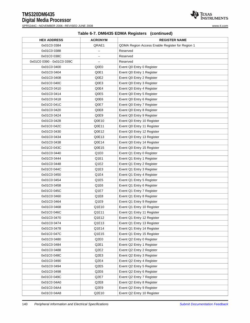
TMS320DM6435Digital Media ProcessorSPRS344C–NOVEMBER 2006–REVISED JUNE 2008 www.ti.com
Table 6-7. DM6435 EDMA Registers (continued)HEX ADDRESS ACRONYM REGISTER NAME
0x01C0 0384 QRAE1 QDMA Region Access Enable Register for Region 10x01C0 0388 – Reserved0x01C0 038C – Reserved
0x01C0 0390 - 0x01C0 039C – Reserved0x01C0 0400 Q0E0 Event Q0 Entry 0 Register0x01C0 0404 Q0E1 Event Q0 Entry 1 Register0x01C0 0408 Q0E2 Event Q0 Entry 2 Register0x01C0 040C Q0E3 Event Q0 Entry 3 Register0x01C0 0410 Q0E4 Event Q0 Entry 4 Register0x01C0 0414 Q0E5 Event Q0 Entry 5 Register0x01C0 0418 Q0E6 Event Q0 Entry 6 Register0x01C0 041C Q0E7 Event Q0 Entry 7 Register0x01C0 0420 Q0E8 Event Q0 Entry 8 Register0x01C0 0424 Q0E9 Event Q0 Entry 9 Register0x01C0 0428 Q0E10 Event Q0 Entry 10 Register0x01C0 042C Q0E11 Event Q0 Entry 11 Register0x01C0 0430 Q0E12 Event Q0 Entry 12 Register0x01C0 0434 Q0E13 Event Q0 Entry 13 Register0x01C0 0438 Q0E14 Event Q0 Entry 14 Register0x01C0 043C Q0E15 Event Q0 Entry 15 Register0x01C0 0440 Q1E0 Event Q1 Entry 0 Register0x01C0 0444 Q1E1 Event Q1 Entry 1 Register0x01C0 0448 Q1E2 Event Q1 Entry 2 Register0x01C0 044C Q1E3 Event Q1 Entry 3 Register0x01C0 0450 Q1E4 Event Q1 Entry 4 Register0x01C0 0454 Q1E5 Event Q1 Entry 5 Register0x01C0 0458 Q1E6 Event Q1 Entry 6 Register0x01C0 045C Q1E7 Event Q1 Entry 7 Register0x01C0 0460 Q1E8 Event Q1 Entry 8 Register0x01C0 0464 Q1E9 Event Q1 Entry 9 Register0x01C0 0468 Q1E10 Event Q1 Entry 10 Register0x01C0 046C Q1E11 Event Q1 Entry 11 Register0x01C0 0470 Q1E12 Event Q1 Entry 12 Register0x01C0 0474 Q1E13 Event Q1 Entry 13 Register0x01C0 0478 Q1E14 Event Q1 Entry 14 Register0x01C0 047C Q1E15 Event Q1 Entry 15 Register0x01C0 0480 Q2E0 Event Q2 Entry 0 Register0x01C0 0484 Q2E1 Event Q2 Entry 1 Register0x01C0 0488 Q2E2 Event Q2 Entry 2 Register0x01C0 048C Q2E3 Event Q2 Entry 3 Register0x01C0 0490 Q2E4 Event Q2 Entry 4 Register0x01C0 0494 Q2E5 Event Q2 Entry 5 Register0x01C0 0498 Q2E6 Event Q2 Entry 6 Register0x01C0 049C Q2E7 Event Q2 Entry 7 Register0x01C0 04A0 Q2E8 Event Q2 Entry 8 Register0x01C0 04A4 Q2E9 Event Q2 Entry 9 Register0x01C0 04A8 Q2E10 Event Q2 Entry 10 Register
Peripheral Information and Electrical Specifications140 Submit Documentation Feedback
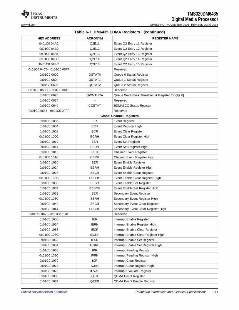
TMS320DM6435Digital Media Processor
www.ti.com SPRS344C–NOVEMBER 2006–REVISED JUNE 2008
Table 6-7. DM6435 EDMA Registers (continued)HEX ADDRESS ACRONYM REGISTER NAME0x01C0 04AC Q2E11 Event Q2 Entry 11 Register0x01C0 04B0 Q2E12 Event Q2 Entry 12 Register0x01C0 04B4 Q2E13 Event Q2 Entry 13 Register0x01C0 04B8 Q2E14 Event Q2 Entry 14 Register0x01C0 04BC Q2E15 Event Q2 Entry 15 Register
0x01C0 04C0 - 0x01C0 05FF Reserved0x01C0 0600 QSTAT0 Queue 0 Status Register0x01C0 0604 QSTAT1 Queue 1 Status Register0x01C0 0608 QSTAT2 Queue 2 Status Register
0x01C0 060C - 0x01C0 061F Reserved0x01C0 0620 QWMTHRA Queue Watermark Threshold A Register for Q[2:0]0x01C0 0624 – Reserved0x01C0 0640 CCSTAT EDMA3CC Status Register
0x01C0 0644 - 0x01C0 0FFF ReservedGlobal Channel Registers
0x01C0 1000 ER Event Register0x01C0 1004 ERH Event Register High0x01C0 1008 ECR Event Clear Register0x01C0 100C ECRH Event Clear Register High0x01C0 1010 ESR Event Set Register0x01C0 1014 ESRH Event Set Register High0x01C0 1018 CER Chained Event Register0x01C0 101C CERH Chained Event Register High0x01C0 1020 EER Event Enable Register0x01C0 1024 EERH Event Enable Register High0x01C0 1028 EECR Event Enable Clear Register0x01C0 102C EECRH Event Enable Clear Register High0x01C0 1030 EESR Event Enable Set Register0x01C0 1034 EESRH Event Enable Set Register High0x01C0 1038 SER Secondary Event Register0x01C0 103C SERH Secondary Event Register High0x01C0 1040 SECR Secondary Event Clear Register0x01C0 1044 SECRH Secondary Event Clear Register High
0x01C0 1048 - 0x01C0 104F Reserved0x01C0 1050 IER Interrupt Enable Register0x01C0 1054 IERH Interrupt Enable Register High0x01C0 1058 IECR Interrupt Enable Clear Register0x01C0 105C IECRH Interrupt Enable Clear Register High0x01C0 1060 IESR Interrupt Enable Set Register0x01C0 1064 IESRH Interrupt Enable Set Register High0x01C0 1068 IPR Interrupt Pending Register0x01C0 106C IPRH Interrupt Pending Register High0x01C0 1070 ICR Interrupt Clear Register0x01C0 1074 ICRH Interrupt Clear Register High0x01C0 1078 IEVAL Interrupt Evaluate Register0x01C0 1080 QER QDMA Event Register0x01C0 1084 QEER QDMA Event Enable Register
Submit Documentation Feedback Peripheral Information and Electrical Specifications 141
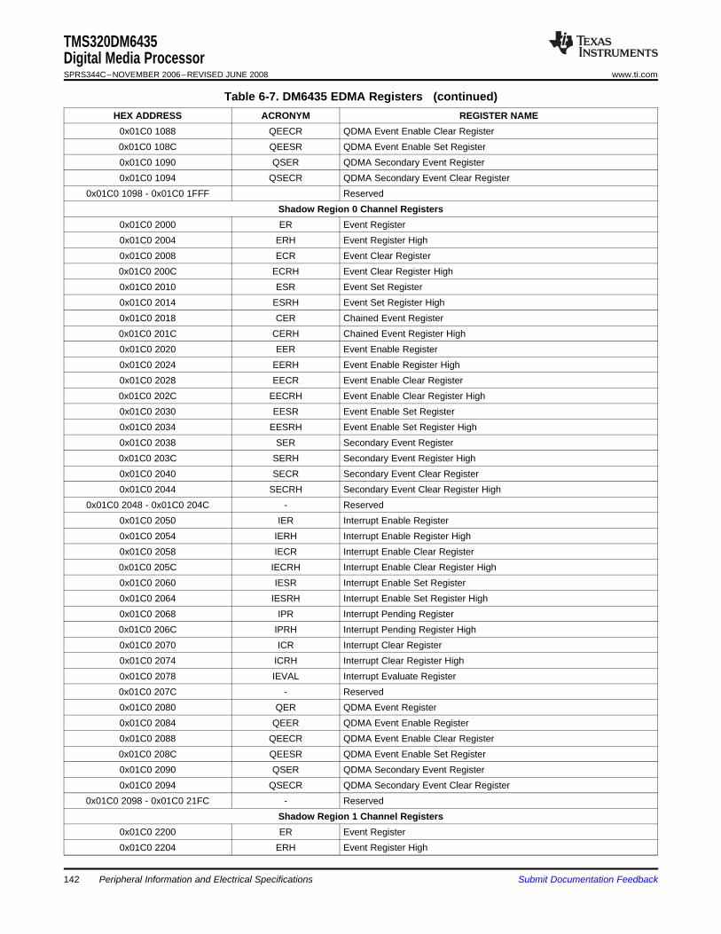
TMS320DM6435Digital Media ProcessorSPRS344C–NOVEMBER 2006–REVISED JUNE 2008 www.ti.com
Table 6-7. DM6435 EDMA Registers (continued)HEX ADDRESS ACRONYM REGISTER NAME
0x01C0 1088 QEECR QDMA Event Enable Clear Register0x01C0 108C QEESR QDMA Event Enable Set Register0x01C0 1090 QSER QDMA Secondary Event Register0x01C0 1094 QSECR QDMA Secondary Event Clear Register
0x01C0 1098 - 0x01C0 1FFF ReservedShadow Region 0 Channel Registers
0x01C0 2000 ER Event Register0x01C0 2004 ERH Event Register High0x01C0 2008 ECR Event Clear Register0x01C0 200C ECRH Event Clear Register High0x01C0 2010 ESR Event Set Register0x01C0 2014 ESRH Event Set Register High0x01C0 2018 CER Chained Event Register0x01C0 201C CERH Chained Event Register High0x01C0 2020 EER Event Enable Register0x01C0 2024 EERH Event Enable Register High0x01C0 2028 EECR Event Enable Clear Register0x01C0 202C EECRH Event Enable Clear Register High0x01C0 2030 EESR Event Enable Set Register0x01C0 2034 EESRH Event Enable Set Register High0x01C0 2038 SER Secondary Event Register0x01C0 203C SERH Secondary Event Register High0x01C0 2040 SECR Secondary Event Clear Register0x01C0 2044 SECRH Secondary Event Clear Register High
0x01C0 2048 - 0x01C0 204C - Reserved0x01C0 2050 IER Interrupt Enable Register0x01C0 2054 IERH Interrupt Enable Register High0x01C0 2058 IECR Interrupt Enable Clear Register0x01C0 205C IECRH Interrupt Enable Clear Register High0x01C0 2060 IESR Interrupt Enable Set Register0x01C0 2064 IESRH Interrupt Enable Set Register High0x01C0 2068 IPR Interrupt Pending Register0x01C0 206C IPRH Interrupt Pending Register High0x01C0 2070 ICR Interrupt Clear Register0x01C0 2074 ICRH Interrupt Clear Register High0x01C0 2078 IEVAL Interrupt Evaluate Register0x01C0 207C - Reserved0x01C0 2080 QER QDMA Event Register0x01C0 2084 QEER QDMA Event Enable Register0x01C0 2088 QEECR QDMA Event Enable Clear Register0x01C0 208C QEESR QDMA Event Enable Set Register0x01C0 2090 QSER QDMA Secondary Event Register0x01C0 2094 QSECR QDMA Secondary Event Clear Register
0x01C0 2098 - 0x01C0 21FC - ReservedShadow Region 1 Channel Registers
0x01C0 2200 ER Event Register0x01C0 2204 ERH Event Register High
Peripheral Information and Electrical Specifications142 Submit Documentation Feedback
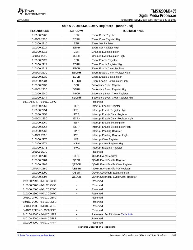
TMS320DM6435Digital Media Processor
www.ti.com SPRS344C–NOVEMBER 2006–REVISED JUNE 2008
Table 6-7. DM6435 EDMA Registers (continued)HEX ADDRESS ACRONYM REGISTER NAME
0x01C0 2208 ECR Event Clear Register0x01C0 220C ECRH Event Clear Register High0x01C0 2210 ESR Event Set Register0x01C0 2214 ESRH Event Set Register High0x01C0 2218 CER Chained Event Register0x01C0 221C CERH Chained Event Register High0x01C0 2220 EER Event Enable Register0x01C0 2224 EERH Event Enable Register High0x01C0 2228 EECR Event Enable Clear Register0x01C0 222C EECRH Event Enable Clear Register High0x01C0 2230 EESR Event Enable Set Register0x01C0 2234 EESRH Event Enable Set Register High0x01C0 2238 SER Secondary Event Register0x01C0 223C SERH Secondary Event Register High0x01C0 2240 SECR Secondary Event Clear Register0x01C0 2244 SECRH Secondary Event Clear Register High
0x01C0 2248 - 0x01C0 224C - Reserved0x01C0 2250 IER Interrupt Enable Register0x01C0 2254 IERH Interrupt Enable Register High0x01C0 2258 IECR Interrupt Enable Clear Register0x01C0 225C IECRH Interrupt Enable Clear Register High0x01C0 2260 IESR Interrupt Enable Set Register0x01C0 2264 IESRH Interrupt Enable Set Register High0x01C0 2268 IPR Interrupt Pending Register0x01C0 226C IPRH Interrupt Pending Register High0x01C0 2270 ICR Interrupt Clear Register0x01C0 2274 ICRH Interrupt Clear Register High0x01C0 2278 IEVAL Interrupt Evaluate Register0x01C0 227C - Reserved0x01C0 2280 QER QDMA Event Register0x01C0 2284 QEER QDMA Event Enable Register0x01C0 2288 QEECR QDMA Event Enable Clear Register0x01C0 228C QEESR QDMA Event Enable Set Register0x01C0 2290 QSER QDMA Secondary Event Register0x01C0 2294 QSECR QDMA Secondary Event Clear Register
0x01C0 2298 - 0x01C0 23FC - Reserved0x01C0 2400 - 0x01C0 25FC - Reserved0x01C0 2600 - 0x01C0 27FC - Reserved0x01C0 2800 - 0x01C0 29FC - Reserved0x01C0 2A00 - 0x01C0 2BFC - Reserved0x01C0 2C00 - 0x01C0 2DFC - Reserved0x01C0 2E00 - 0x01C0 2FFC - Reserved0x01C0 2FFD - 0x01C0 3FFF - Reserved0x01C0 4000 - 0x01C0 4FFF - Parameter Set RAM (see Table 6-8)0x01C0 5000 - 0x01C0 7FFF - Reserved0x01C0 8000 - 0x01C0 FFFF - Reserved
Transfer Controller 0 Registers
Submit Documentation Feedback Peripheral Information and Electrical Specifications 143
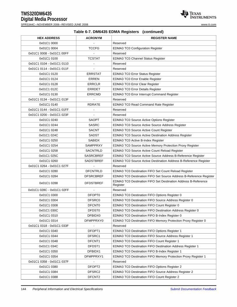
TMS320DM6435Digital Media ProcessorSPRS344C–NOVEMBER 2006–REVISED JUNE 2008 www.ti.com
Table 6-7. DM6435 EDMA Registers (continued)HEX ADDRESS ACRONYM REGISTER NAME
0x01C1 0000 - Reserved0x01C1 0004 TCCFG EDMA3 TC0 Configuration Register
0x01C1 0008 - 0x01C1 00FF - Reserved0x01C1 0100 TCSTAT EDMA3 TC0 Channel Status Register
0x01C1 0104 - 0x01C1 0110 - Reserved0x01C1 0114 - 0x01C1 011F - Reserved
0x01C1 0120 ERRSTAT EDMA3 TC0 Error Status Register0x01C1 0124 ERREN EDMA3 TC0 Error Enable Register0x01C1 0128 ERRCLR EDMA3 TC0 Error Clear Register0x01C1 012C ERRDET EDMA3 TC0 Error Details Register0x01C1 0130 ERRCMD EDMA3 TC0 Error Interrupt Command Register
0x01C1 0134 - 0x01C1 013F - Reserved0x01C1 0140 RDRATE EDMA3 TC0 Read Command Rate Register
0x01C1 0144 - 0x01C1 01FF - Reserved0x01C1 0200 - 0x01C1 023F - Reserved
0x01C1 0240 SAOPT EDMA3 TC0 Source Active Options Register0x01C1 0244 SASRC EDMA3 TC0 Source Active Source Address Register0x01C1 0248 SACNT EDMA3 TC0 Source Active Count Register0x01C1 024C SADST EDMA3 TC0 Source Active Destination Address Register0x01C1 0250 SABIDX EDMA3 TC0 Active B-Index Register0x01C1 0254 SAMPPRXY EDMA3 TC0 Source Active Memory Protection Proxy Register0x01C1 0258 SACNTRLD EDMA3 TC0 Source Active Count Reload Register0x01C1 025C SASRCBREF EDMA3 TC0 Source Active Source Address B-Reference Register0x01C1 0260 SADSTBREF EDMA3 TC0 Source Active Destination Address B-Reference Register
0x01C1 0264 - 0x01C1 027F - Reserved0x01C1 0280 DFCNTRLD EDMA3 TC0 Destination FIFO Set Count Reload Register0x01C1 0284 DFSRCBREF EDMA3 TC0 Destination FIFO Set Source Address B-Reference Register
EDMA3 TC0 Destination FIFO Set Destination Address B-Reference0x01C1 0288 DFDSTBREF Register0x01C1 028C - 0x01C1 02FF - Reserved
0x01C1 0300 DFOPT0 EDMA3 TC0 Destination FIFO Options Register 00x01C1 0304 DFSRC0 EDMA3 TC0 Destination FIFO Source Address Register 00x01C1 0308 DFCNT0 EDMA3 TC0 Destination FIFO Count Register 00x01C1 030C DFDST0 EDMA3 TC0 Destination FIFO Destination Address Register 00x01C1 0310 DFBIDX0 EDMA3 TC0 Destination FIFO B-Index Register 00x01C1 0314 DFMPPRXY0 EDMA3 TC0 Destination FIFO Memory Protection Proxy Register 0
0x01C1 0318 - 0x01C1 033F - Reserved0x01C1 0340 DFOPT1 EDMA3 TC0 Destination FIFO Options Register 10x01C1 0344 DFSRC1 EDMA3 TC0 Destination FIFO Source Address Register 10x01C1 0348 DFCNT1 EDMA3 TC0 Destination FIFO Count Register 10x01C1 034C DFDST1 EDMA3 TC0 Destination FIFO Destination Address Register 10x01C1 0350 DFBIDX1 EDMA3 TC0 Destination FIFO B-Index Register 10x01C1 0354 DFMPPRXY1 EDMA3 TC0 Destination FIFO Memory Protection Proxy Register 1
0x01C1 0358 - 0x01C1 037F - Reserved0x01C1 0380 DFOPT2 EDMA3 TC0 Destination FIFO Options Register 20x01C1 0384 DFSRC2 EDMA3 TC0 Destination FIFO Source Address Register 20x01C1 0388 DFCNT2 EDMA3 TC0 Destination FIFO Count Register 2
Peripheral Information and Electrical Specifications144 Submit Documentation Feedback
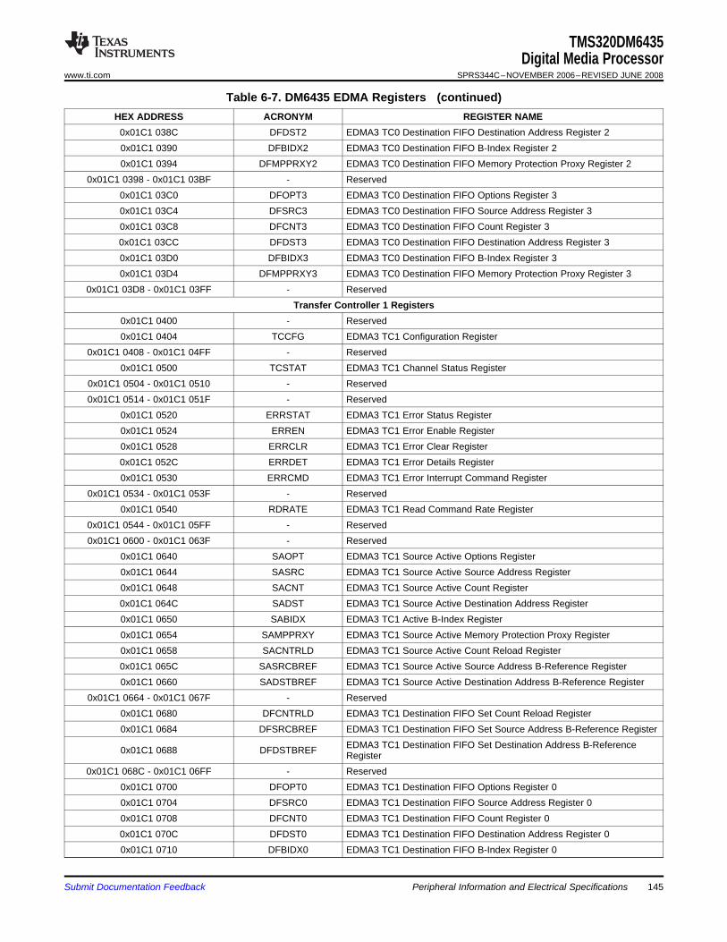
TMS320DM6435Digital Media Processor
www.ti.com SPRS344C–NOVEMBER 2006–REVISED JUNE 2008
Table 6-7. DM6435 EDMA Registers (continued)HEX ADDRESS ACRONYM REGISTER NAME
0x01C1 038C DFDST2 EDMA3 TC0 Destination FIFO Destination Address Register 20x01C1 0390 DFBIDX2 EDMA3 TC0 Destination FIFO B-Index Register 20x01C1 0394 DFMPPRXY2 EDMA3 TC0 Destination FIFO Memory Protection Proxy Register 2
0x01C1 0398 - 0x01C1 03BF - Reserved0x01C1 03C0 DFOPT3 EDMA3 TC0 Destination FIFO Options Register 30x01C1 03C4 DFSRC3 EDMA3 TC0 Destination FIFO Source Address Register 30x01C1 03C8 DFCNT3 EDMA3 TC0 Destination FIFO Count Register 30x01C1 03CC DFDST3 EDMA3 TC0 Destination FIFO Destination Address Register 30x01C1 03D0 DFBIDX3 EDMA3 TC0 Destination FIFO B-Index Register 30x01C1 03D4 DFMPPRXY3 EDMA3 TC0 Destination FIFO Memory Protection Proxy Register 3
0x01C1 03D8 - 0x01C1 03FF - ReservedTransfer Controller 1 Registers
0x01C1 0400 - Reserved0x01C1 0404 TCCFG EDMA3 TC1 Configuration Register
0x01C1 0408 - 0x01C1 04FF - Reserved0x01C1 0500 TCSTAT EDMA3 TC1 Channel Status Register
0x01C1 0504 - 0x01C1 0510 - Reserved0x01C1 0514 - 0x01C1 051F - Reserved
0x01C1 0520 ERRSTAT EDMA3 TC1 Error Status Register0x01C1 0524 ERREN EDMA3 TC1 Error Enable Register0x01C1 0528 ERRCLR EDMA3 TC1 Error Clear Register0x01C1 052C ERRDET EDMA3 TC1 Error Details Register0x01C1 0530 ERRCMD EDMA3 TC1 Error Interrupt Command Register
0x01C1 0534 - 0x01C1 053F - Reserved0x01C1 0540 RDRATE EDMA3 TC1 Read Command Rate Register
0x01C1 0544 - 0x01C1 05FF - Reserved0x01C1 0600 - 0x01C1 063F - Reserved
0x01C1 0640 SAOPT EDMA3 TC1 Source Active Options Register0x01C1 0644 SASRC EDMA3 TC1 Source Active Source Address Register0x01C1 0648 SACNT EDMA3 TC1 Source Active Count Register0x01C1 064C SADST EDMA3 TC1 Source Active Destination Address Register0x01C1 0650 SABIDX EDMA3 TC1 Active B-Index Register0x01C1 0654 SAMPPRXY EDMA3 TC1 Source Active Memory Protection Proxy Register0x01C1 0658 SACNTRLD EDMA3 TC1 Source Active Count Reload Register0x01C1 065C SASRCBREF EDMA3 TC1 Source Active Source Address B-Reference Register0x01C1 0660 SADSTBREF EDMA3 TC1 Source Active Destination Address B-Reference Register
0x01C1 0664 - 0x01C1 067F - Reserved0x01C1 0680 DFCNTRLD EDMA3 TC1 Destination FIFO Set Count Reload Register0x01C1 0684 DFSRCBREF EDMA3 TC1 Destination FIFO Set Source Address B-Reference Register
EDMA3 TC1 Destination FIFO Set Destination Address B-Reference0x01C1 0688 DFDSTBREF Register0x01C1 068C - 0x01C1 06FF - Reserved
0x01C1 0700 DFOPT0 EDMA3 TC1 Destination FIFO Options Register 00x01C1 0704 DFSRC0 EDMA3 TC1 Destination FIFO Source Address Register 00x01C1 0708 DFCNT0 EDMA3 TC1 Destination FIFO Count Register 00x01C1 070C DFDST0 EDMA3 TC1 Destination FIFO Destination Address Register 00x01C1 0710 DFBIDX0 EDMA3 TC1 Destination FIFO B-Index Register 0
Submit Documentation Feedback Peripheral Information and Electrical Specifications 145
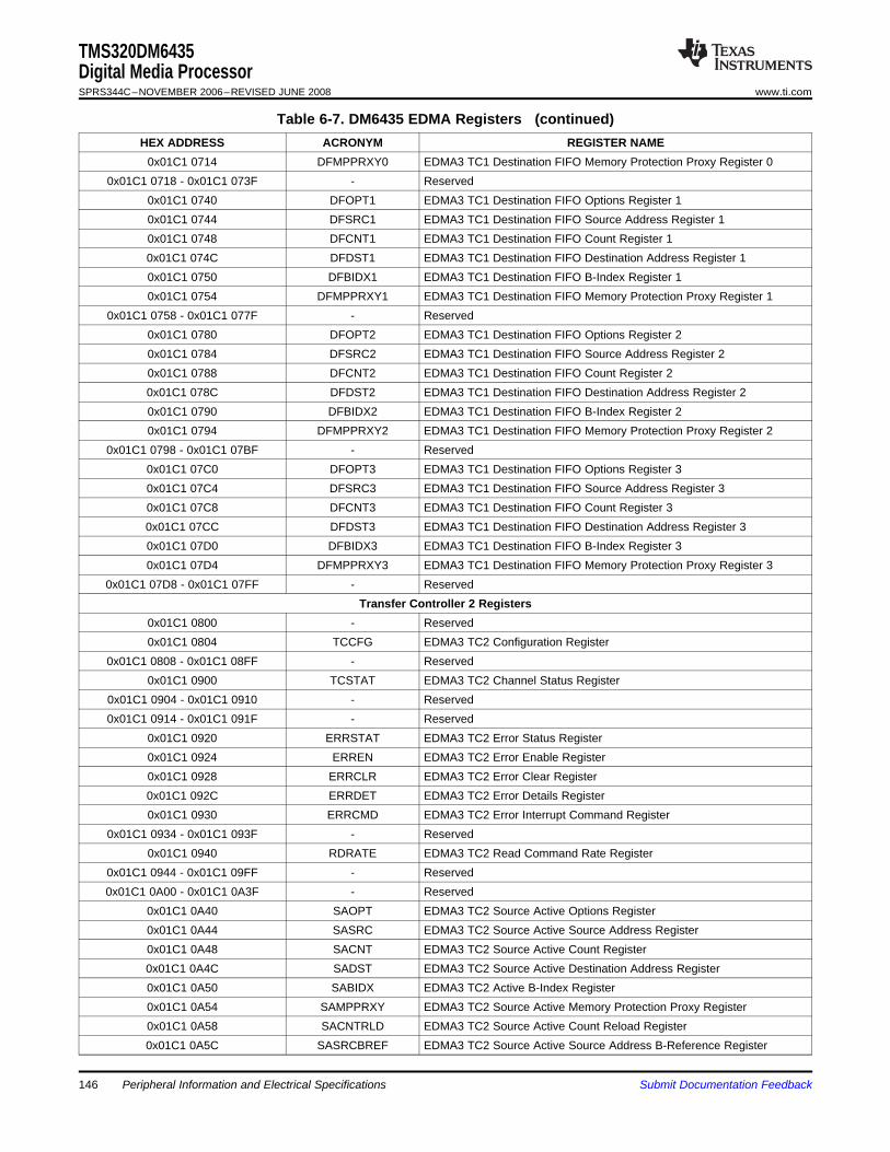
TMS320DM6435Digital Media ProcessorSPRS344C–NOVEMBER 2006–REVISED JUNE 2008 www.ti.com
Table 6-7. DM6435 EDMA Registers (continued)HEX ADDRESS ACRONYM REGISTER NAME
0x01C1 0714 DFMPPRXY0 EDMA3 TC1 Destination FIFO Memory Protection Proxy Register 00x01C1 0718 - 0x01C1 073F - Reserved
0x01C1 0740 DFOPT1 EDMA3 TC1 Destination FIFO Options Register 10x01C1 0744 DFSRC1 EDMA3 TC1 Destination FIFO Source Address Register 10x01C1 0748 DFCNT1 EDMA3 TC1 Destination FIFO Count Register 10x01C1 074C DFDST1 EDMA3 TC1 Destination FIFO Destination Address Register 10x01C1 0750 DFBIDX1 EDMA3 TC1 Destination FIFO B-Index Register 10x01C1 0754 DFMPPRXY1 EDMA3 TC1 Destination FIFO Memory Protection Proxy Register 1
0x01C1 0758 - 0x01C1 077F - Reserved0x01C1 0780 DFOPT2 EDMA3 TC1 Destination FIFO Options Register 20x01C1 0784 DFSRC2 EDMA3 TC1 Destination FIFO Source Address Register 20x01C1 0788 DFCNT2 EDMA3 TC1 Destination FIFO Count Register 20x01C1 078C DFDST2 EDMA3 TC1 Destination FIFO Destination Address Register 20x01C1 0790 DFBIDX2 EDMA3 TC1 Destination FIFO B-Index Register 20x01C1 0794 DFMPPRXY2 EDMA3 TC1 Destination FIFO Memory Protection Proxy Register 2
0x01C1 0798 - 0x01C1 07BF - Reserved0x01C1 07C0 DFOPT3 EDMA3 TC1 Destination FIFO Options Register 30x01C1 07C4 DFSRC3 EDMA3 TC1 Destination FIFO Source Address Register 30x01C1 07C8 DFCNT3 EDMA3 TC1 Destination FIFO Count Register 30x01C1 07CC DFDST3 EDMA3 TC1 Destination FIFO Destination Address Register 30x01C1 07D0 DFBIDX3 EDMA3 TC1 Destination FIFO B-Index Register 30x01C1 07D4 DFMPPRXY3 EDMA3 TC1 Destination FIFO Memory Protection Proxy Register 3
0x01C1 07D8 - 0x01C1 07FF - ReservedTransfer Controller 2 Registers
0x01C1 0800 - Reserved0x01C1 0804 TCCFG EDMA3 TC2 Configuration Register
0x01C1 0808 - 0x01C1 08FF - Reserved0x01C1 0900 TCSTAT EDMA3 TC2 Channel Status Register
0x01C1 0904 - 0x01C1 0910 - Reserved0x01C1 0914 - 0x01C1 091F - Reserved
0x01C1 0920 ERRSTAT EDMA3 TC2 Error Status Register0x01C1 0924 ERREN EDMA3 TC2 Error Enable Register0x01C1 0928 ERRCLR EDMA3 TC2 Error Clear Register0x01C1 092C ERRDET EDMA3 TC2 Error Details Register0x01C1 0930 ERRCMD EDMA3 TC2 Error Interrupt Command Register
0x01C1 0934 - 0x01C1 093F - Reserved0x01C1 0940 RDRATE EDMA3 TC2 Read Command Rate Register
0x01C1 0944 - 0x01C1 09FF - Reserved0x01C1 0A00 - 0x01C1 0A3F - Reserved
0x01C1 0A40 SAOPT EDMA3 TC2 Source Active Options Register0x01C1 0A44 SASRC EDMA3 TC2 Source Active Source Address Register0x01C1 0A48 SACNT EDMA3 TC2 Source Active Count Register0x01C1 0A4C SADST EDMA3 TC2 Source Active Destination Address Register0x01C1 0A50 SABIDX EDMA3 TC2 Active B-Index Register0x01C1 0A54 SAMPPRXY EDMA3 TC2 Source Active Memory Protection Proxy Register0x01C1 0A58 SACNTRLD EDMA3 TC2 Source Active Count Reload Register0x01C1 0A5C SASRCBREF EDMA3 TC2 Source Active Source Address B-Reference Register
Peripheral Information and Electrical Specifications146 Submit Documentation Feedback
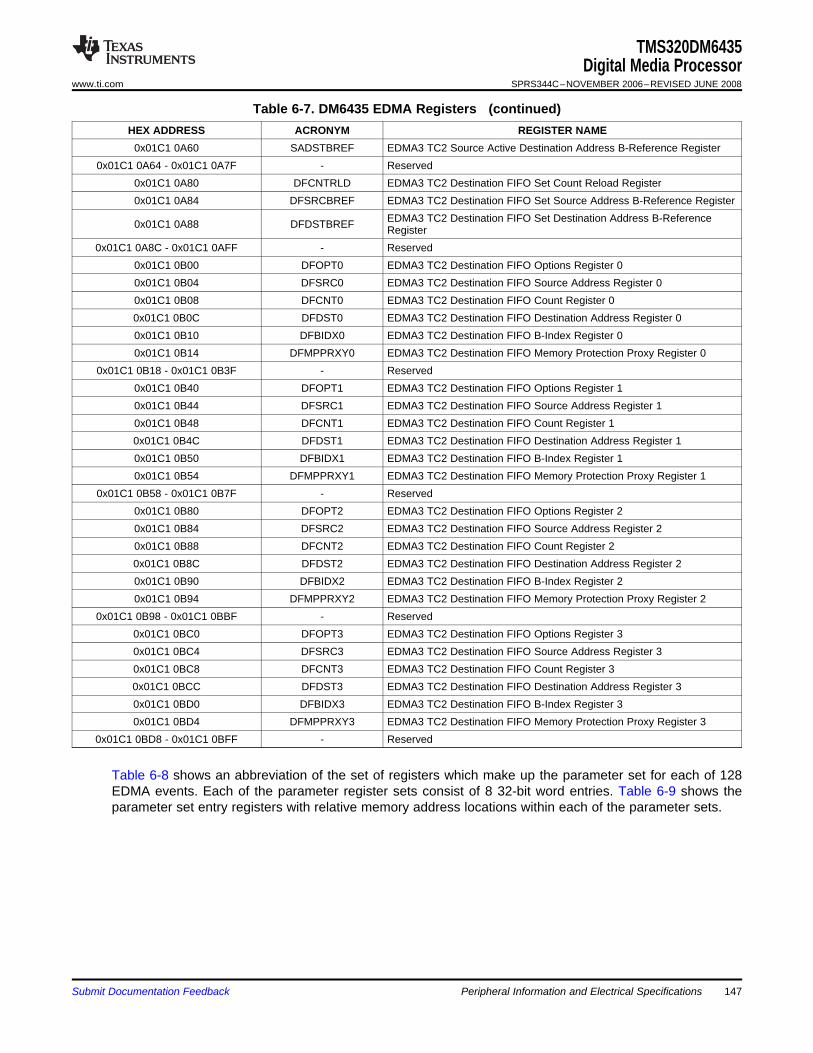
TMS320DM6435Digital Media Processor
www.ti.com SPRS344C–NOVEMBER 2006–REVISED JUNE 2008
Table 6-7. DM6435 EDMA Registers (continued)HEX ADDRESS ACRONYM REGISTER NAME
0x01C1 0A60 SADSTBREF EDMA3 TC2 Source Active Destination Address B-Reference Register0x01C1 0A64 - 0x01C1 0A7F - Reserved
0x01C1 0A80 DFCNTRLD EDMA3 TC2 Destination FIFO Set Count Reload Register0x01C1 0A84 DFSRCBREF EDMA3 TC2 Destination FIFO Set Source Address B-Reference Register
EDMA3 TC2 Destination FIFO Set Destination Address B-Reference0x01C1 0A88 DFDSTBREF Register0x01C1 0A8C - 0x01C1 0AFF - Reserved
0x01C1 0B00 DFOPT0 EDMA3 TC2 Destination FIFO Options Register 00x01C1 0B04 DFSRC0 EDMA3 TC2 Destination FIFO Source Address Register 00x01C1 0B08 DFCNT0 EDMA3 TC2 Destination FIFO Count Register 00x01C1 0B0C DFDST0 EDMA3 TC2 Destination FIFO Destination Address Register 00x01C1 0B10 DFBIDX0 EDMA3 TC2 Destination FIFO B-Index Register 00x01C1 0B14 DFMPPRXY0 EDMA3 TC2 Destination FIFO Memory Protection Proxy Register 0
0x01C1 0B18 - 0x01C1 0B3F - Reserved0x01C1 0B40 DFOPT1 EDMA3 TC2 Destination FIFO Options Register 10x01C1 0B44 DFSRC1 EDMA3 TC2 Destination FIFO Source Address Register 10x01C1 0B48 DFCNT1 EDMA3 TC2 Destination FIFO Count Register 10x01C1 0B4C DFDST1 EDMA3 TC2 Destination FIFO Destination Address Register 10x01C1 0B50 DFBIDX1 EDMA3 TC2 Destination FIFO B-Index Register 10x01C1 0B54 DFMPPRXY1 EDMA3 TC2 Destination FIFO Memory Protection Proxy Register 1
0x01C1 0B58 - 0x01C1 0B7F - Reserved0x01C1 0B80 DFOPT2 EDMA3 TC2 Destination FIFO Options Register 20x01C1 0B84 DFSRC2 EDMA3 TC2 Destination FIFO Source Address Register 20x01C1 0B88 DFCNT2 EDMA3 TC2 Destination FIFO Count Register 20x01C1 0B8C DFDST2 EDMA3 TC2 Destination FIFO Destination Address Register 20x01C1 0B90 DFBIDX2 EDMA3 TC2 Destination FIFO B-Index Register 20x01C1 0B94 DFMPPRXY2 EDMA3 TC2 Destination FIFO Memory Protection Proxy Register 2
0x01C1 0B98 - 0x01C1 0BBF - Reserved0x01C1 0BC0 DFOPT3 EDMA3 TC2 Destination FIFO Options Register 30x01C1 0BC4 DFSRC3 EDMA3 TC2 Destination FIFO Source Address Register 30x01C1 0BC8 DFCNT3 EDMA3 TC2 Destination FIFO Count Register 30x01C1 0BCC DFDST3 EDMA3 TC2 Destination FIFO Destination Address Register 30x01C1 0BD0 DFBIDX3 EDMA3 TC2 Destination FIFO B-Index Register 30x01C1 0BD4 DFMPPRXY3 EDMA3 TC2 Destination FIFO Memory Protection Proxy Register 3
0x01C1 0BD8 - 0x01C1 0BFF - Reserved
Table 6-8 shows an abbreviation of the set of registers which make up the parameter set for each of 128EDMA events. Each of the parameter register sets consist of 8 32-bit word entries. Table 6-9 shows theparameter set entry registers with relative memory address locations within each of the parameter sets.
Submit Documentation Feedback Peripheral Information and Electrical Specifications 147
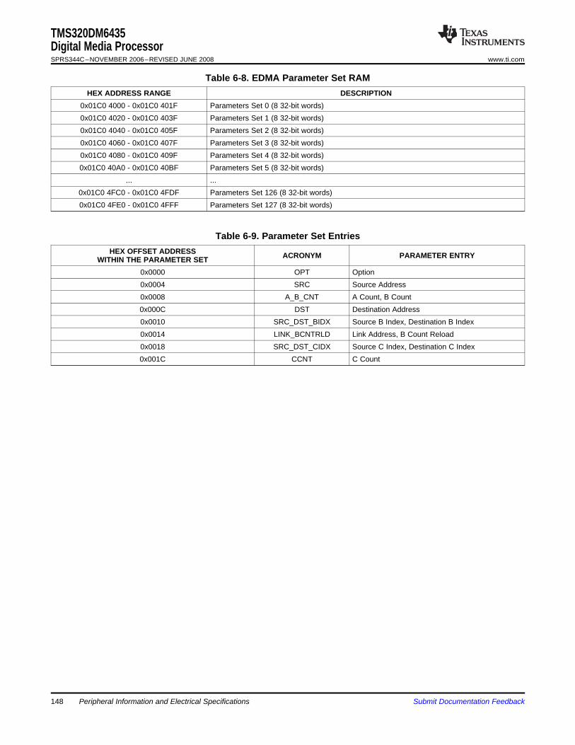
TMS320DM6435Digital Media ProcessorSPRS344C–NOVEMBER 2006–REVISED JUNE 2008 www.ti.com
Table 6-8. EDMA Parameter Set RAMHEX ADDRESS RANGE DESCRIPTION
0x01C0 4000 - 0x01C0 401F Parameters Set 0 (8 32-bit words)0x01C0 4020 - 0x01C0 403F Parameters Set 1 (8 32-bit words)0x01C0 4040 - 0x01C0 405F Parameters Set 2 (8 32-bit words)0x01C0 4060 - 0x01C0 407F Parameters Set 3 (8 32-bit words)0x01C0 4080 - 0x01C0 409F Parameters Set 4 (8 32-bit words)0x01C0 40A0 - 0x01C0 40BF Parameters Set 5 (8 32-bit words)
... ...0x01C0 4FC0 - 0x01C0 4FDF Parameters Set 126 (8 32-bit words)0x01C0 4FE0 - 0x01C0 4FFF Parameters Set 127 (8 32-bit words)
Table 6-9. Parameter Set EntriesHEX OFFSET ADDRESS ACRONYM PARAMETER ENTRYWITHIN THE PARAMETER SET
0x0000 OPT Option0x0004 SRC Source Address0x0008 A_B_CNT A Count, B Count0x000C DST Destination Address0x0010 SRC_DST_BIDX Source B Index, Destination B Index0x0014 LINK_BCNTRLD Link Address, B Count Reload0x0018 SRC_DST_CIDX Source C Index, Destination C Index0x001C CCNT C Count
Peripheral Information and Electrical Specifications148 Submit Documentation Feedback
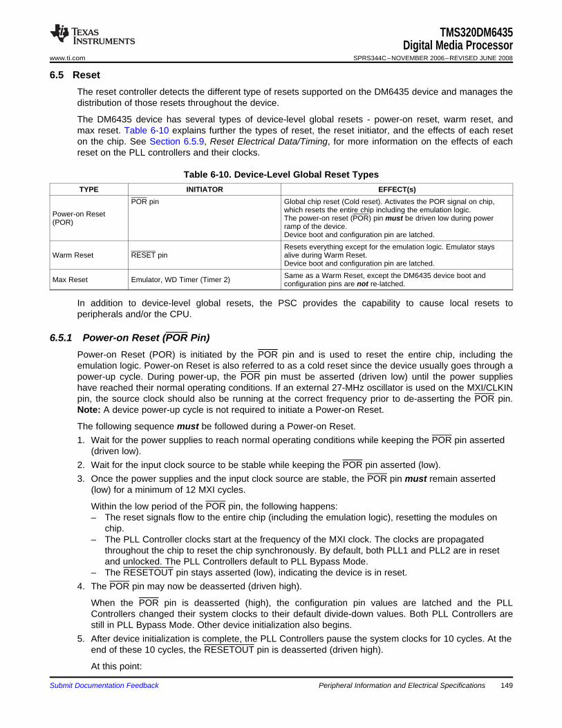
6.5 Reset
6.5.1 Power-on Reset (POR Pin)
TMS320DM6435Digital Media Processor
www.ti.com SPRS344C–NOVEMBER 2006–REVISED JUNE 2008
The reset controller detects the different type of resets supported on the DM6435 device and manages thedistribution of those resets throughout the device.
The DM6435 device has several types of device-level global resets - power-on reset, warm reset, andmax reset. Table 6-10 explains further the types of reset, the reset initiator, and the effects of each reseton the chip. See Section 6.5.9, Reset Electrical Data/Timing, for more information on the effects of eachreset on the PLL controllers and their clocks.
Table 6-10. Device-Level Global Reset TypesTYPE INITIATOR EFFECT(s)
POR pin Global chip reset (Cold reset). Activates the POR signal on chip,which resets the entire chip including the emulation logic.Power-on Reset The power-on reset (POR) pin must be driven low during power(POR) ramp of the device.Device boot and configuration pin are latched.Resets everything except for the emulation logic. Emulator stays
Warm Reset RESET pin alive during Warm Reset.Device boot and configuration pin are latched.Same as a Warm Reset, except the DM6435 device boot andMax Reset Emulator, WD Timer (Timer 2) configuration pins are not re-latched.
In addition to device-level global resets, the PSC provides the capability to cause local resets toperipherals and/or the CPU.
Power-on Reset (POR) is initiated by the POR pin and is used to reset the entire chip, including theemulation logic. Power-on Reset is also referred to as a cold reset since the device usually goes through apower-up cycle. During power-up, the POR pin must be asserted (driven low) until the power supplieshave reached their normal operating conditions. If an external 27-MHz oscillator is used on the MXI/CLKINpin, the source clock should also be running at the correct frequency prior to de-asserting the POR pin.Note: A device power-up cycle is not required to initiate a Power-on Reset.
The following sequence must be followed during a Power-on Reset.1. Wait for the power supplies to reach normal operating conditions while keeping the POR pin asserted
(driven low).2. Wait for the input clock source to be stable while keeping the POR pin asserted (low).3. Once the power supplies and the input clock source are stable, the POR pin must remain asserted
(low) for a minimum of 12 MXI cycles.
Within the low period of the POR pin, the following happens:– The reset signals flow to the entire chip (including the emulation logic), resetting the modules on
chip.– The PLL Controller clocks start at the frequency of the MXI clock. The clocks are propagated
throughout the chip to reset the chip synchronously. By default, both PLL1 and PLL2 are in resetand unlocked. The PLL Controllers default to PLL Bypass Mode.
– The RESETOUT pin stays asserted (low), indicating the device is in reset.4. The POR pin may now be deasserted (driven high).
When the POR pin is deasserted (high), the configuration pin values are latched and the PLLControllers changed their system clocks to their default divide-down values. Both PLL Controllers arestill in PLL Bypass Mode. Other device initialization also begins.
5. After device initialization is complete, the PLL Controllers pause the system clocks for 10 cycles. At theend of these 10 cycles, the RESETOUT pin is deasserted (driven high).
At this point:
Submit Documentation Feedback Peripheral Information and Electrical Specifications 149
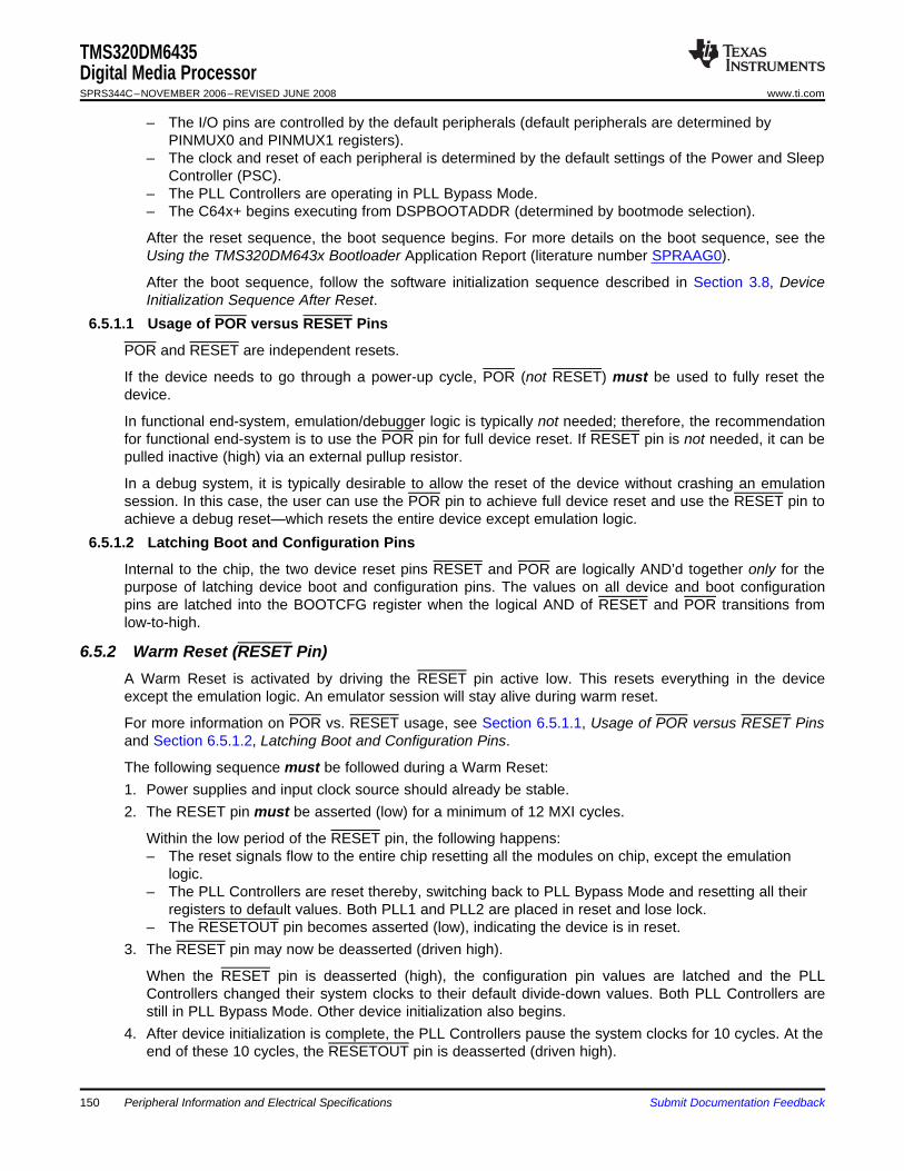
6.5.1.1 Usage of POR versus RESET Pins
6.5.1.2 Latching Boot and Configuration Pins
6.5.2 Warm Reset (RESET Pin)
TMS320DM6435Digital Media ProcessorSPRS344C–NOVEMBER 2006–REVISED JUNE 2008 www.ti.com
– The I/O pins are controlled by the default peripherals (default peripherals are determined byPINMUX0 and PINMUX1 registers).
– The clock and reset of each peripheral is determined by the default settings of the Power and SleepController (PSC).
– The PLL Controllers are operating in PLL Bypass Mode.– The C64x+ begins executing from DSPBOOTADDR (determined by bootmode selection).
After the reset sequence, the boot sequence begins. For more details on the boot sequence, see theUsing the TMS320DM643x Bootloader Application Report (literature number SPRAAG0).
After the boot sequence, follow the software initialization sequence described in Section 3.8, DeviceInitialization Sequence After Reset.
POR and RESET are independent resets.
If the device needs to go through a power-up cycle, POR (not RESET) must be used to fully reset thedevice.
In functional end-system, emulation/debugger logic is typically not needed; therefore, the recommendationfor functional end-system is to use the POR pin for full device reset. If RESET pin is not needed, it can bepulled inactive (high) via an external pullup resistor.
In a debug system, it is typically desirable to allow the reset of the device without crashing an emulationsession. In this case, the user can use the POR pin to achieve full device reset and use the RESET pin toachieve a debug reset—which resets the entire device except emulation logic.
Internal to the chip, the two device reset pins RESET and POR are logically AND’d together only for thepurpose of latching device boot and configuration pins. The values on all device and boot configurationpins are latched into the BOOTCFG register when the logical AND of RESET and POR transitions fromlow-to-high.
A Warm Reset is activated by driving the RESET pin active low. This resets everything in the deviceexcept the emulation logic. An emulator session will stay alive during warm reset.
For more information on POR vs. RESET usage, see Section 6.5.1.1, Usage of POR versus RESET Pinsand Section 6.5.1.2, Latching Boot and Configuration Pins.
The following sequence must be followed during a Warm Reset:1. Power supplies and input clock source should already be stable.2. The RESET pin must be asserted (low) for a minimum of 12 MXI cycles.
Within the low period of the RESET pin, the following happens:– The reset signals flow to the entire chip resetting all the modules on chip, except the emulation
logic.– The PLL Controllers are reset thereby, switching back to PLL Bypass Mode and resetting all their
registers to default values. Both PLL1 and PLL2 are placed in reset and lose lock.– The RESETOUT pin becomes asserted (low), indicating the device is in reset.
3. The RESET pin may now be deasserted (driven high).
When the RESET pin is deasserted (high), the configuration pin values are latched and the PLLControllers changed their system clocks to their default divide-down values. Both PLL Controllers arestill in PLL Bypass Mode. Other device initialization also begins.
4. After device initialization is complete, the PLL Controllers pause the system clocks for 10 cycles. At theend of these 10 cycles, the RESETOUT pin is deasserted (driven high).
Peripheral Information and Electrical Specifications150 Submit Documentation Feedback
6.5.3 Maximum Reset
TMS320DM6435Digital Media Processor
www.ti.com SPRS344C–NOVEMBER 2006–REVISED JUNE 2008
At this point:– The I/O pins are controlled by the default peripherals (default peripherals are determined by
PINMUX0 and PINMUX1 registers).– The clock and reset of each peripheral is determined by the default settings of the Power and Sleep
Controller (PSC).– The PLL Controllers are operating in PLL Bypass Mode.– The C64x+ begins executing from DSPBOOTADDR (determined by bootmode selection).
After the reset sequence, the boot sequence begins. For more details on the boot sequence, see theUsing the TMS320DM643x Bootloader Application Report (literature number SPRAAG0)).
After the boot sequence, follow the software initialization sequence described in Section 3.8, DeviceInitialization Sequence After Reset.
A Maximum (Max) Reset is initiated by the emulator or the watchdog timer (Timer 2). The effects are thesame as a warm reset, except the device boot and configuration pins are not re-latched. The emulatorinitiates a maximum reset via the ICEPICK module. This ICEPICK initiated reset is non-maskable. Whenthe watchdog timer counter reaches zero, this will also initiate a maximum reset to recover from a runawaycondition. The watchdog timeout reset condition is masked if the TIMERCTL.WDRST bit is cleared to "0".
To invoke the maximum reset via the ICEPICK module, the user can perform the following from the CodeComposer Studio™ IDE menu: Debug→Advanced Resets→System Reset
This is the Max Reset sequence:1. Max Reset is initiated by the emulator or the watchdog timer.
During this time, the following happens:– The reset signals flow to the entire chip resetting all the modules on chip except the emulation
logic.– The PLL Controllers are reset thereby, switching back to PLL Bypass Mode and resetting all their
registers to default values. Both PLL1 and PLL2 are placed in reset and lose lock.– The RESETOUT pin becomes asserted (low), indicating the device is in reset.
2. After device initialization is complete, the PLL Controllers pause the system clocks for 10 cycles. At theend of these 10 cycles, the RESETOUT pin is deasserted (driven high).
At this point:– The I/O pins are controlled by the default peripherals (default peripherals are determined by
PINMUX0 and PINMUX1 registers).– The clock and reset of each peripheral is determined by the default settings of the Power and Sleep
Controller (PSC).– The PLL Controllers are operating in PLL Bypass Mode.– The C64x+ begins executing from DSPBOOTADDR (determined by bootmode selection).
After the reset sequence, the boot sequence begins. Since the boot and configuration pins are not latchedwith a Max Reset, the previous values (as shown in the BOOTCFG register) are used to select the bootmode. For more details on the boot sequence, see the Using the TMS320DM643x Bootloader ApplicationReport (literature number SPRAAG0).
After the boot sequence, follow the software initialization sequence described in Section 3.8, DeviceInitialization Sequence After Reset.
Submit Documentation Feedback Peripheral Information and Electrical Specifications 151
6.5.4 CPU Local Reset
6.5.5 Peripheral Local Reset
6.5.6 Reset Priority
6.5.7 Reset Controller Register
6.5.8 Pin Behaviors at Reset
TMS320DM6435Digital Media ProcessorSPRS344C–NOVEMBER 2006–REVISED JUNE 2008 www.ti.com
The C64x+ DSP CPU has an internal reset input that allows a host (HPI) to control it. This reset isconfigured through a register bit (MDCTL[39].LRST) in the Power Sleep Controller (PSC) module. When inC64x+ local reset, the slave DMA port on C64x+ will remain active and the internal memory will beaccessible. For procedures on asserting and de-asserting CPU local reset by the host, see theTMS320DM643x DMP DSP Subsystem Reference Guide (literature number SPRU978).
For information on peripheral selection at the rising edge of POR or RESET, see Section 3, DeviceConfigurations of this data manual.
The user can configure the local reset and clock state of a peripheral through programming the PSC.Table 6-4, DM6435 LPSC Assignments identifies the LPSC numbers and the peripherals capable of beinglocally reset by the PSC. For more detailed information on the programming of these peripherals by thePSC, see the TMS320DM643x DMP DSP Subsystem Reference Guide (literature number SPRU978).
If any of the above reset sources occur simultaneously, the PLLC only processes the highest priority resetrequest. The reset request priorities are as follows (high to low):• Power-on Reset• Maximum Reset• Warm Reset• CPU Reset
The Reset Type Status (RSTYPE) register (01C4 00E4) is the only register for the reset controller. Thisregister falls in the same memory range as the PLL1 controller registers (see Table 6-18 for the PLL1Controller Registers (including Reset Controller)). For more details on the RSTYPE register, see theTMS320DM643x DMP DSP Subsystem Reference Guide (literature number SPRU978).
During normal operations, pins are controlled by the respective peripheral selected in the PINMUX0 orPINMUX1 register. During device level global reset, the pin behaves as follows:
Multiplexed Boot and Configuration Pins
These pins are forced 3-stated when RESETOUT is asserted (low). This is to ensure the proper boot andconfiguration values can be latched on these multiplexed pins. This is particularly useful in the case wherethe boot and configuration values are driven by an external control device. After RESETOUT isdeasserted (high), these pins are controlled by their respective default peripheral.• Boot and Configuration Pins Group: GP[28], GP[27], GP[26]/(FASTBOOT), GP[25]/(BOOTMODE3),
GP[24]/(BOOTMODE2), GP[23]/(BOOTMODE1), GP[22]/(BOOTMODE0),EM_A[4]/GP[10]/(AEAW2/PLLMS2), EM_A[1]/(ALE)/GP[9]/(AEAW1/PLLMS1),EM_A[2]/(CLE)/GP[8]/(AEAW0/PLLMS0), EM_A[0]/GP[7]/(AEM2), EM_BA[0]/GP[6]/(AEM1), andEM_BA[1]/GP[5]/(AEM0).
For information on whether external pullup/pulldown resistors should be used on the boot andconfiguration pins, see Section 3.9.1, Pullup/Pulldown Resistors.
152 Peripheral Information and Electrical Specifications Submit Documentation Feedback
TMS320DM6435Digital Media Processor
www.ti.com SPRS344C–NOVEMBER 2006–REVISED JUNE 2008
Default Power Down Pins
As discussed in Section 3.2, Power Considerations, the VDD3P3V_PWDN register controls power to the3.3-V pins. The VDD3P3V_PWDN register defaults to powering down some 3.3-V pins to save power. Formore details on the VDD3P3V_PWDN register and which 3.3-V pins default to powerup or powerdown,Section 3.2, Power Considerations. The pins that default to powerdown, are both reset to powerdown andhigh-impedance. They remain in that state until configured otherwise by VDD3P3_PWDN andPINMUX0/PINMUX1 programming.• Default Power Down Pin Group: GP[4]/PWM1, ACLKR0/CLKX0/GP[99], AFSR0/DR0/GP[100],
AHCLKR0/CLKR0/GP[101], AXR0[3]/FSR0/GP[102], AXR0[2]/FSX0/GP[103], AXR0[1]/DX0/GP[104],AXR0/GP[105], ACLKX0/GP[106], AFSX0/GP[107], AHCLKX0/GP[108], AMUTEIN0/GP[109],AMUTE0/GP[110], HECC_TX/TOUT1L/UTXD1/GP[55], HECC_RX/TINP1L/URXD1/GP[56],CLKS0/TOUT0L/GP[97], TINP0L/GP[98], URXD0/GP[85], UTXD0/GP[86], UCTS0/GP[87], andURTS0/PWM0/GP[88].
All Other Pins
During RESETOUT assertion (low), all other pins are controlled by the default peripheral. The defaultperipheral is determined by the default settings of the PINMUX0 or PINMUX1 registers.
Some of the PINMUX0/PINMUX1 settings are determined by configuration pins latched at reset. Todetermine the reset behavior of these pins, see Section 3.7, Multiplexed Pin Configurations and read therest of the this subsection to understand how that default peripheral controls the pin.
The reset behaviors for all these other pins are categorized as follows (also see Figure 6-7 and Figure 6-8in Section 6.5.9, Reset Electrical Data/Timing):• Z+/Low Group (Z Longer-to-Low Group): These pins are 3-stated when device-level global reset
source (e.g., POR, RESET, or Max Reset) is asserted. These pins remain 3-stated throughoutRESETOUT assertion. When RESETOUT is deasserted, these pins drive a logic low.
• Z+/High Group (Z Longer-to-High Group): These pins are 3-stated when device-level global resetsource (e.g., POR, RESET, or Max Reset) is asserted. These pins remain 3-stated throughoutRESETOUT assertion. When RESETOUT is deasserted, these pins drive a logic high.
• Z+/Invalid Group (Z Longer-to-Invalid Group): These pins are 3-stated when device-level globalreset source (e.g., POR, RESET, or Max Reset) is asserted. These pins remain 3-stated throughoutRESETOUT assertion. When RESETOUT is deasserted, these pins drive an invalid value untilconfigured otherwise by their respective peripheral (after the peripheral is enabled by the PSC).
• Z Group: These pins are 3-stated by default, and these pins remain 3-stated throughout RESETOUTassertion. When RESETOUT is deasserted, these pins remain 3-stated until configured otherwise bytheir respective peripheral (after the peripheral is enabled by the PSC).
• Low Group: These pins are low by default, and remain low until configured otherwise by theirrespective peripheral (after the peripheral is enabled by the PSC).
• High Group: These pins are high by default, and remain high until configured otherwise by theirrespective peripheral (after the peripheral is enabled by the PSC).
• Z/Low Group (Z-to-Low Group): These pins are 3-stated when device-level global reset source (e.g.,POR, RESET, or Max Reset) is asserted. When the reset source is deasserted, these pins drive alogic low.
• Z/High Group (Z-to-High Group): These pins are 3-stated when device-level global reset source(e.g., POR, RESET, or Max Reset) is asserted. When reset source is deasserted, these pins drive alogic high.
• Clock Group: These clock pins are toggling by default. They paused momentarily before RESETOUTis deasserted (high). The only pin in the Clock Group is CLKOUT0.
This is a list of possible default peripherals and how they control the pins during reset:• GPIO: All GPIO pins behave according to Z Group.
Note: The following EMIFA list only includes pins that can default to function as EMIFA signals.
Submit Documentation Feedback Peripheral Information and Electrical Specifications 153
6.5.9 Reset Electrical Data/Timing
TMS320DM6435Digital Media ProcessorSPRS344C–NOVEMBER 2006–REVISED JUNE 2008 www.ti.com
• EMIFA: These EMIFA signals are multiplexed with boot and configuration pins: EM_A[4], EM_A[2:0],EM_BA[0], EM_BA[1]; therefore, they are forced 3-stated throughout RESETOUT.– Z+/Low Group: EM_A[4], EM_A[2:0]– Z+/High Group: EM_BA[0], EM_BA[1], EM_OE, EM_WE– Z+/Invalid Group: EM_D[7:0]– Z/Low Group: EM_A[21:5], EM_A[3], EM_R/W– Z/High Group: EM_CS2– Z Group: EM_WAIT/(RDY/BSY)
• DDR2 Memory Controller:– Clock Group: DDR_CLK, DDR_CLK– DDR2 Z Group: DDR_DQM[3:0], DDR_DQS[3:0], DDR_D[31:0]– DDR2 Low Group: DDR_CKE, DDR_BA[2:0], DDR_A[12:0]– DDR2 High Group: DDR_CS, DDR_WE, DDR_RAS, DDR_CAS
• I2C: All I2C pins behave according to Z Group.• JTAG: TDO, EMU0, and EMU1 pins behave according to Z Group. TCK, TDI, TMS, and TRST are
input-only pins.• Clock: CLKOUT0
For more information on the pin behaviors during device-level global reset, see Figure 6-7 and Figure 6-8in Section 6.5.9, Reset Electrical Data/Timing.
Note: If a configuration pin must be routed out from the device, the internal pullup/pulldown (IPU/IPD)resistor should not be relied upon; TI recommends the use of an external pullup/pulldown resistor.
Table 6-11. Timing Requirements for Reset (see Figure 6-7 and Figure 6-8)-7/-6/-5/-4
-L/-Q6/-Q5/-Q4NO. UNITMIN MAX
1 tw(RESET) Pulse duration, POR low or RESET low 12C (1) nsSetup time, boot and configuration pins valid before POR high or RESET4 tsu(CONFIG) 12C (1) nshigh (2)
Hold time, boot and configuration pins valid after POR high or RESET5 th(CONFIG) 0 nshigh (2)
(1) C = 1/MXI clock frequency in ns. The device clock source must be stable and at a valid frequency prior to meeting the tw(RESET)requirement.
(2) For the list of boot and configuration pins, see Table 2-5, Boot Terminal Functions.
Table 6-12. Switching Characteristics Over Recommended Operating Conditions During Reset (1)
(see Figure 6-8)-7/-6/-5/-4
-L/-Q6/-Q5/-Q4NO. PARAMETER UNITMIN MAX
2 td(RSTH-RSTOUTH) Delay time, POR high or RESET high to RESETOUT high 1900C ns3 tw(PAUSE) Pulse duration, SYSCLKs paused (low) before RESETOUT high 10C 10C ns6 td(RSTL-IV) Delay time, POR low or RESET low to pins invalid 20 ns7 td(RSTH-V) Delay time, POR high or RESET high to pins valid 20 ns8 td(RSTOUTH-V) Delay time, RESETOUT high to pins valid 0 ns9 td(RSTOUTH-IV) Delay time, RESETOUT high to pins invalid 12C ns
(1) C = 1/CLKIN1 clock frequency in ns.
Peripheral Information and Electrical Specifications154 Submit Documentation Feedback
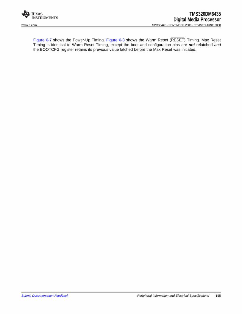
TMS320DM6435Digital Media Processor
www.ti.com SPRS344C–NOVEMBER 2006–REVISED JUNE 2008
Figure 6-7 shows the Power-Up Timing. Figure 6-8 shows the Warm Reset (RESET) Timing. Max ResetTiming is identical to Warm Reset Timing, except the boot and configuration pins are not relatched andthe BOOTCFG register retains its previous value latched before the Max Reset was initiated.
Submit Documentation Feedback Peripheral Information and Electrical Specifications 155
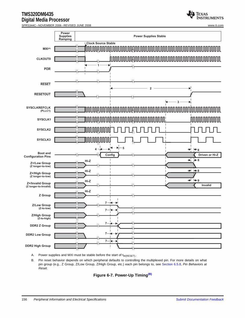
MXI(A)
POR
RESET
RESETOUT
SYSCLKREFCLK(PLLC1)
SYSCLK1
SYSCLK2
SYSCLK3
CLKOUT0
Boot andConfiguration Pins
Config
Z+/Low Group(Z longer-to-low)
Z+/High Group(Z longer-to-low)
Z Group
PowerSuppliesRamping
Power Supplies Stable
Hi-Z
Hi-Z
Hi-Z
Clock Source Stable
1
4 5
2
3
8
8
8
DDR2 Z Group
DDR2 Low Group
DDR2 High Group
Driven or Hi-Z
Z/High Group(Z-to-high)
Z/Low Group(Z-to-low)
7
7
7
7
7
Z+/Invalid Group(Z longer-to-Invalid)
Hi-Z 9
Invalid
TMS320DM6435Digital Media ProcessorSPRS344C–NOVEMBER 2006–REVISED JUNE 2008 www.ti.com
A. Power supplies and MXI must be stable before the start of tW(RESET)..B. Pin reset behavior depends on which peripheral defaults to controlling the multiplexed pin. For more details on what
pin group (e.g., Z Group, Z/Low Group, Z/High Group, etc.) each pin belongs to, see Section 6.5.8, Pin Behaviors atReset.
Figure 6-7. Power-Up Timing(B)
Peripheral Information and Electrical Specifications156 Submit Documentation Feedback
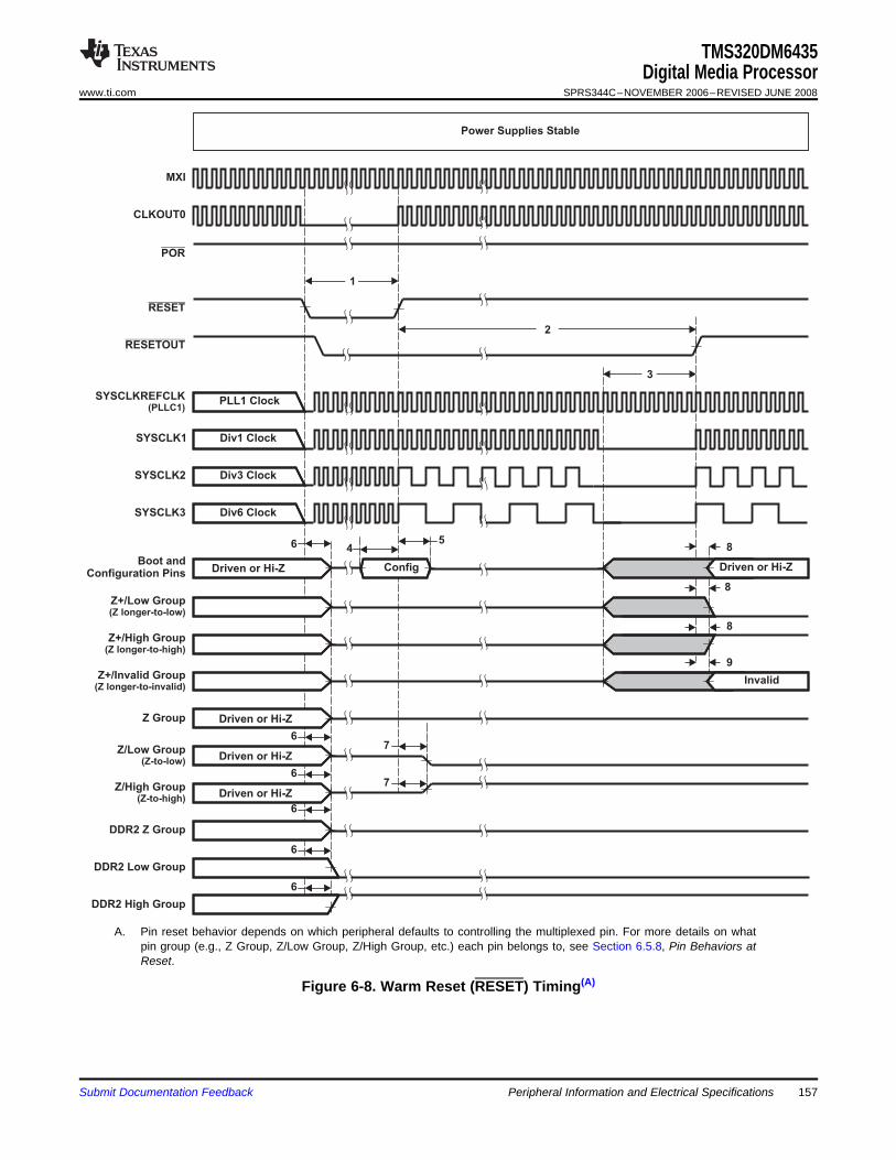
MXI
POR
RESET
RESETOUT
SYSCLKREFCLK(PLLC1)
SYSCLK1
SYSCLK2
SYSCLK3
CLKOUT0
Boot andConfiguration Pins
Config
Power Supplies Stable
1
45
2
3
PLL1 Clock
Div1 Clock
Div3 Clock
Div6 Clock
Driven or Hi-Z
86
Driven or Hi-Z
Z+/Low Group(Z longer-to-low)
Z+/High Group(Z longer-to-high)
Z Group
8
DDR2 Z Group
DDR2 Low Group
DDR2 High Group
Z/High Group(Z-to-high)
7
Z/Low Group(Z-to-low)
7
Driven or Hi-Z
Driven or Hi-Z
Driven or Hi-Z
6
6
6
6
6
8
Z+/Invalid Group(Z longer-to-invalid)
9
Invalid
TMS320DM6435Digital Media Processor
www.ti.com SPRS344C–NOVEMBER 2006–REVISED JUNE 2008
A. Pin reset behavior depends on which peripheral defaults to controlling the multiplexed pin. For more details on whatpin group (e.g., Z Group, Z/Low Group, Z/High Group, etc.) each pin belongs to, see Section 6.5.8, Pin Behaviors atReset.
Figure 6-8. Warm Reset (RESET) Timing(A)
Submit Documentation Feedback Peripheral Information and Electrical Specifications 157
6.6 External Clock Input From MXI/CLKIN Pin
6.6.1 Clock Input Option 1—Crystal
MXI/CLKIN MXO
C1 C2
Crystal27 MHz
MXVSS
1.8 V
MXVDD
CLC1C2
(C1 C2)
TMS320DM6435Digital Media ProcessorSPRS344C–NOVEMBER 2006–REVISED JUNE 2008 www.ti.com
The DM6435 device includes two options to provide an external clock input:• Use an on-chip oscillator with external crystal.• Use an external 1.8-V LVCMOS-compatible clock input.
The optimal external clock input frequency is 27 MHz. Section 6.6.1 provides more details on Option 1,using an on-chip oscillator with external crystal. Section 6.6.2 provides details on Option 2, using anexternal 1.8-V LVCMOS-compatible clock input.
In this option, a crystal is used as the external clock input to the DM6435.
The 27-MHz oscillator provides the reference clock for all DM6435 subsystems and peripherals. Theon-chip oscillator requires an external 27-MHz crystal connected across the MXI and MXO pins, alongwith two load capacitors, as shown in Figure 6-9. The external crystal load capacitors must be connectedonly to the 27-MHz oscillator ground pin (MXVSS). Do not connect to board ground (VSS). The MXVDD pincan be connected to the same 1.8 V power supply as DVDDR2.
Figure 6-9. 27-MHz System Oscillator
The load capacitors, C1 and C2, should be chosen such that the equation is satisfied (typical values areC1 = C2 = 10 pF). CL in the equation is the load specified by the crystal manufacturer. All discretecomponents used to implement the oscillator circuit should be placed as close as possible to theassociated oscillator pins (MXI and MXO) and to the MXVSS pin.
Table 6-13. Input Requirements for CrystalPARAMETER MIN TYP MAX UNIT
Start-up time (from power up until oscillating at stable frequency of 27 4 msMHz)Oscillaton frequency 27 MHzESR 60 Ω
Frequency Stability (1) ±50 ppm
(1) For video and audio applications, stability of the input clock is very important. The user should select crystals with low enough ppm toensure good video and audio quality for the specific application.
Peripheral Information and Electrical Specifications158 Submit Documentation Feedback
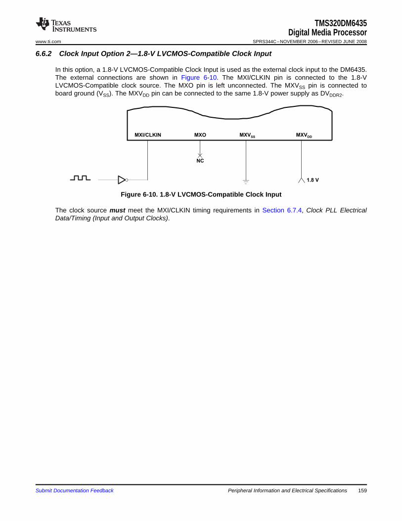
6.6.2 Clock Input Option 2—1.8-V LVCMOS-Compatible Clock Input
MXI/CLKIN MXO
NC
MXVSS
1.8 V
MXVDD
TMS320DM6435Digital Media Processor
www.ti.com SPRS344C–NOVEMBER 2006–REVISED JUNE 2008
In this option, a 1.8-V LVCMOS-Compatible Clock Input is used as the external clock input to the DM6435.The external connections are shown in Figure 6-10. The MXI/CLKIN pin is connected to the 1.8-VLVCMOS-Compatible clock source. The MXO pin is left unconnected. The MXVSS pin is connected toboard ground (VSS). The MXVDD pin can be connected to the same 1.8-V power supply as DVDDR2.
Figure 6-10. 1.8-V LVCMOS-Compatible Clock Input
The clock source must meet the MXI/CLKIN timing requirements in Section 6.7.4, Clock PLL ElectricalData/Timing (Input and Output Clocks).
Submit Documentation Feedback Peripheral Information and Electrical Specifications 159
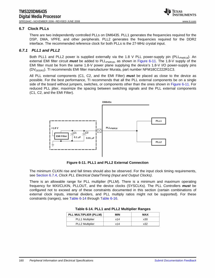
6.7 Clock PLLs
6.7.1 PLL1 and PLL2
PLLPWR18
C2C1EMI Filter
+1.8 V
0.01 F
DM643x
PLL2
PLL1
0.1 F
TMS320DM6435Digital Media ProcessorSPRS344C–NOVEMBER 2006–REVISED JUNE 2008 www.ti.com
There are two independently controlled PLLs on DM6435. PLL1 generates the frequencies required for theDSP, DMA, VPFE, and other peripherals. PLL2 generates the frequencies required for the DDR2interface. The recommended reference clock for both PLLs is the 27-MHz crystal input.
Both PLL1 and PLL2 power is supplied externally via the 1.8 V PLL power-supply pin (PLLPWR18). Anexternal EMI filter circuit must be added to PLLPWR18, as shown in Figure 6-11. The 1.8-V supply of theEMI filter must be from the same 1.8-V power plane supplying the device’s 1.8-V I/O power-supply pins(DVDDDR2). TI recommends EMI filter manufacturer Murata, part number NFM18CC222R1C3.
All PLL external components (C1, C2, and the EMI Filter) must be placed as close to the device aspossible. For the best performance, TI recommends that all the PLL external components be on a singleside of the board without jumpers, switches, or components other than the ones shown in Figure 6-11. Forreduced PLL jitter, maximize the spacing between switching signals and the PLL external components(C1, C2, and the EMI Filter).
Figure 6-11. PLL1 and PLL2 External Connection
The minimum CLKIN rise and fall times should also be observed. For the input clock timing requirements,see Section 6.7.4, Clock PLL Electrical Data/Timing (Input and Output Clocks).
There is an allowable range for PLL multiplier (PLLM). There is a minimum and maximum operatingfrequency for MXI/CLKIN, PLLOUT, and the device clocks (SYSCLKs). The PLL Controllers must beconfigured not to exceed any of these constraints documented in this section (certain combinations ofexternal clock inputs, internal dividers, and PLL multiply ratios might not be supported). For theseconstraints (ranges), see Table 6-14 through Table 6-16.
Table 6-14. PLL1 and PLL2 Multiplier RangesPLL MULTIPLIER (PLLM) MIN MAX
PLL1 Multiplier x14 x30PLL2 Multiplier x14 x32
Peripheral Information and Electrical Specifications160 Submit Documentation Feedback
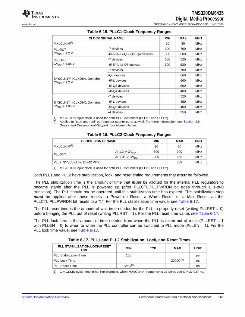
TMS320DM6435Digital Media Processor
www.ti.com SPRS344C–NOVEMBER 2006–REVISED JUNE 2008
Table 6-15. PLLC1 Clock Frequency RangesCLOCK SIGNAL NAME MIN MAX UNIT
MXI/CLKIN (1) 20 30 MHz-7 devices 300 700 MHzPLLOUT
CVDD = 1.2 V -6/-5/-4/-L/-Q6/-Q5/-Q4 devices 300 600 MHz-7 devices 300 520 MHzPLLOUT
CVDD = 1.05 V -6/-5/-4/-L/-Q5 devices 300 520 MHz-7 devices 700 MHz-Q6 devices 660 MHz
SYSCLK1 (2) (CLKDIV1 Domain) -6/-L devices 600 MHzCVDD = 1.2 V-5/-Q5 devices 500 MHz-4/-Q4 devices 400 MHz-7 devices 520 MHz-6/-L devices 450 MHzSYSCLK1 (2) (CLKDIV1 Domain),
CVDD = 1.05 V -5/-Q5 devices 400 MHz-4 devices 350 MHz
(1) MXI/CLKIN input clock is used for both PLL Controllers (PLLC1 and PLLC2).(2) Applies to "tape and reel" part number counterparts as well. For more information, see Section 2.8,
Device and Development-Support Tool Nomenclature.
Table 6-16. PLLC2 Clock Frequency RangesCLOCK SIGNAL NAME MIN MAX UNIT
MXI/CLKIN (1) 20 30 MHzAt 1.2-V CVDD 300 900 MHz
PLLOUTAt 1.05-V CVDD 300 666 MHz
PLL2_SYSCLK1 (to DDR2 PHY) 333 MHz
(1) MXI/CLKIN input clock is used for both PLL Controllers (PLLC1 and PLLC2).
Both PLL1 and PLL2 have stabilization, lock, and reset timing requirements that must be followed.
The PLL stabilization time is the amount of time that must be allotted for the internal PLL regulators tobecome stable after the PLL is powered up (after PLLCTL.PLLPWRDN bit goes through a 1-to-0transition). The PLL should not be operated until this stabilization time has expired. This stabilization stepmust be applied after these resets—a Power-on Reset, a Warm Reset, or a Max Reset, as thePLLCTL.PLLPWRDN bit resets to a "1". For the PLL stabliziation time value, see Table 6-17.
The PLL reset time is the amount of wait time needed for the PLL to properly reset (writing PLLRST = 0)before bringing the PLL out of reset (writing PLLRST = 1). For the PLL reset time value, see Table 6-17.
The PLL lock time is the amount of time needed from when the PLL is taken out of reset (PLLRST = 1with PLLEN = 0) to when to when the PLL controller can be switched to PLL mode (PLLEN = 1). For thePLL lock time value, see Table 6-17.
Table 6-17. PLL1 and PLL2 Stabilization, Lock, and Reset TimesPLL STABILIZATION/LOCK/RESET MIN TYP MAX UNITTIME
PLL Stabilization Time 150 µsPLL Lock Time 2000C (1) nsPLL Reset Time 128C (1) ns
(1) C = CLKIN cycle time in ns. For example, when MXI/CLKIN frequency is 27 MHz, use C = 37.037 ns.
Submit Documentation Feedback Peripheral Information and Electrical Specifications 161
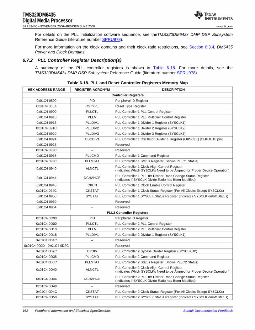
6.7.2 PLL Controller Register Description(s)
TMS320DM6435Digital Media ProcessorSPRS344C–NOVEMBER 2006–REVISED JUNE 2008 www.ti.com
For details on the PLL initialization software sequence, see theTMS320DM643x DMP DSP SubsystemReference Guide (literature number SPRU978).
For more information on the clock domains and their clock ratio restrictions, see Section 6.3.4, DM6435Power and Clock Domains.
A summary of the PLL controller registers is shown in Table 6-18. For more details, see theTMS320DM643x DMP DSP Subsystem Reference Guide (literature number SPRU978).
Table 6-18. PLL and Reset Controller Registers Memory MapHEX ADDRESS RANGE REGISTER ACRONYM DESCRIPTION
Controller Registers0x01C4 0800 PID Peripheral ID Register0x01C4 08E4 RSTYPE Reset Type Register0x01C4 0900 PLLCTL PLL Controller 1 PLL Control Register0x01C4 0910 PLLM PLL Controller 1 PLL Multiplier Control Register0x01C4 0918 PLLDIV1 PLL Controller 1 Divider 1 Register (SYSCLK1)0x01C4 091C PLLDIV2 PLL Controller 1 Divider 2 Register (SYSCLK2)0x01C4 0920 PLLDIV3 PLL Controller 1 Divider 3 Register (SYSCLK3)0x01C4 0924 OSCDIV1 PLL Controller 1 Oscillator Divider 1 Register (OBSCLK) [CLKOUT0 pin]0x01C4 0928 – Reserved0x01C4 092C – Reserved0x01C4 0938 PLLCMD PLL Controller 1 Command Register0x01C4 093C PLLSTAT PLL Controller 1 Status Register (Shows PLLC1 Status)
PLL Controller 1 Clock Align Control Register0x01C4 0940 ALNCTL (Indicates Which SYSCLKs Need to be Aligned for Proper Device Operation)PLL Controller 1 PLLDIV Divider Ratio Change Status Register0x01C4 0944 DCHANGE (Indicates if SYSCLK Divide Ratio has Been Modified)
0x01C4 0948 CKEN PLL Controller 1 Clock Enable Control Register0x01C4 094C CKSTAT PLL Controller 1 Clock Status Register (For All Clocks Except SYSCLKx)0x01C4 0950 SYSTAT PLL Controller 1 SYSCLK Status Register (Indicates SYSCLK on/off Status)0x01C4 0960 – Reserved0x01C4 0964 – Reserved
PLL2 Controller Registers0x01C4 0C00 PID Peripheral ID Register0x01C4 0D00 PLLCTL PLL Controller 2 PLL Control Register0x01C4 0D10 PLLM PLL Controller 2 PLL Multiplier Control Register0x01C4 0D18 PLLDIV1 PLL Controller 2 Divider 1 Register (SYSCLK1)0x01C4 0D1C – Reserved
0x01C4 0D20 - 0x01C4 0D2C – Reserved0x01C4 0D2C BPDIV PLL Controller 2 Bypass Divider Register (SYSCLKBP)0x01C4 0D38 PLLCMD PLL Controller 2 Command Register0x01C4 0D3C PLLSTAT PLL Controller 2 Status Register (Shows PLLC2 Status)
PLL Controller 2 Clock Align Control Register0x01C4 0D40 ALNCTL (Indicates Which SYSCLKs Need to be Aligned for Proper Device Operation)PLL Controller 2 PLLDIV Divider Ratio Change Status Register0x01C4 0D44 DCHANGE (Indicates if SYSCLK Divide Ratio has Been Modified)
0x01C4 0D48 – Reserved0x01C4 0D4C CKSTAT PLL Controller 2 Clock Status Register (For All Clocks Except SYSCLKx)0x01C4 0D50 SYSTAT PLL Controller 2 SYSCLK Status Register (Indicates SYSCLK on/off Status)
Peripheral Information and Electrical Specifications162 Submit Documentation Feedback
6.7.3 Clock PLL Considerations with External Clock Sources
TMS320DM6435Digital Media Processor
www.ti.com SPRS344C–NOVEMBER 2006–REVISED JUNE 2008
Table 6-18. PLL and Reset Controller Registers Memory Map (continued)HEX ADDRESS RANGE REGISTER ACRONYM DESCRIPTION
0x01C4 0D54 - 0x01C4 0FFF – Reserved
If the internal oscillator is bypassed, to minimize the clock jitter a single clean power supply should powerboth the DM6435 device and the external clock oscillator circuit. The minimum CLKIN rise and fall timesshould also be observed. For the input clock timing requirements, see Section 6.7.4, Clock PLL ElectricalData/Timing (Input and Output Clocks).
Rise/fall times, duty cycles (high/low pulse durations), and the load capacitance of the external clocksource must meet the device requirements in this data manual (see Section 5.3, Electrical CharacteristicsOver Recommended Ranges of Supply Voltage and Operating Temperature and Section 6.7.4, Clock PLLElectrical Data/Timing (Input and Output Clocks).
Submit Documentation Feedback Peripheral Information and Electrical Specifications 163
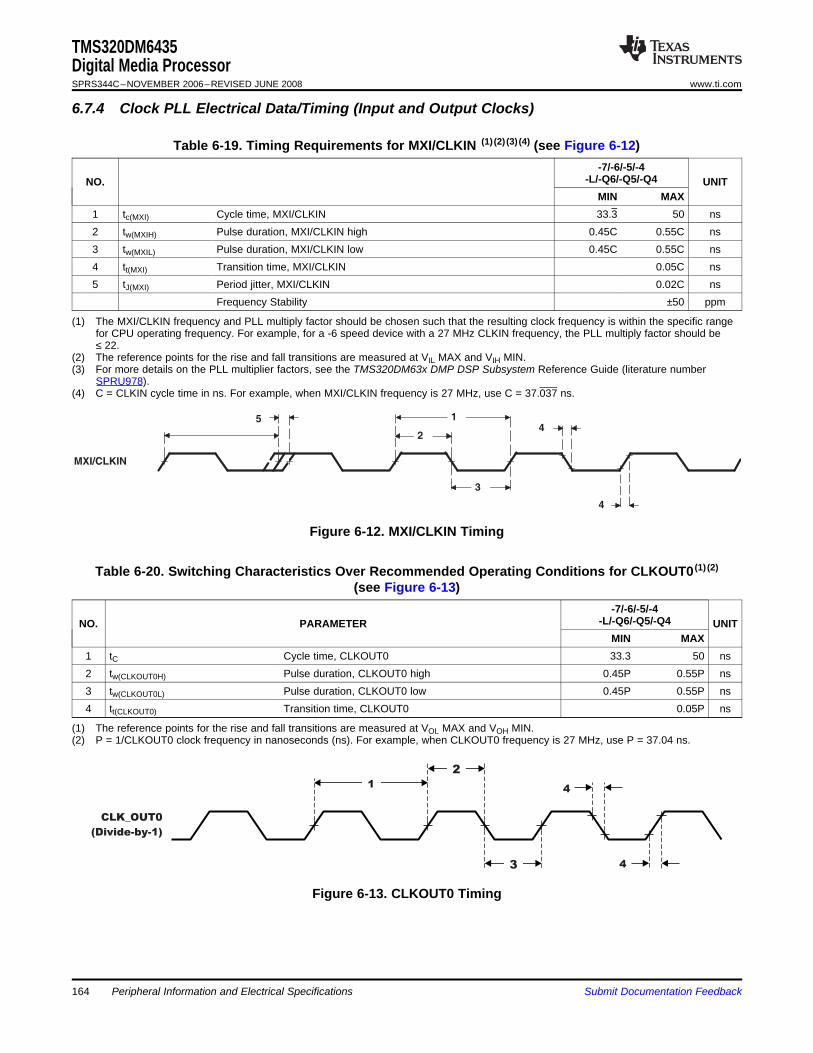
6.7.4 Clock PLL Electrical Data/Timing (Input and Output Clocks)
MXI/CLKIN
2
3
4
4
5 1
CLK_OUT0
(Divide-by-1)
4
4
2
1
3
TMS320DM6435Digital Media ProcessorSPRS344C–NOVEMBER 2006–REVISED JUNE 2008 www.ti.com
Table 6-19. Timing Requirements for MXI/CLKIN (1) (2) (3) (4) (see Figure 6-12)-7/-6/-5/-4
-L/-Q6/-Q5/-Q4NO. UNITMIN MAX
1 tc(MXI) Cycle time, MXI/CLKIN 33.3 50 ns2 tw(MXIH) Pulse duration, MXI/CLKIN high 0.45C 0.55C ns3 tw(MXIL) Pulse duration, MXI/CLKIN low 0.45C 0.55C ns4 tt(MXI) Transition time, MXI/CLKIN 0.05C ns5 tJ(MXI) Period jitter, MXI/CLKIN 0.02C ns
Frequency Stability ±50 ppm
(1) The MXI/CLKIN frequency and PLL multiply factor should be chosen such that the resulting clock frequency is within the specific rangefor CPU operating frequency. For example, for a -6 speed device with a 27 MHz CLKIN frequency, the PLL multiply factor should be≤ 22.
(2) The reference points for the rise and fall transitions are measured at VIL MAX and VIH MIN.(3) For more details on the PLL multiplier factors, see the TMS320DM63x DMP DSP Subsystem Reference Guide (literature number
SPRU978).(4) C = CLKIN cycle time in ns. For example, when MXI/CLKIN frequency is 27 MHz, use C = 37.037 ns.
Figure 6-12. MXI/CLKIN Timing
Table 6-20. Switching Characteristics Over Recommended Operating Conditions for CLKOUT0 (1) (2)
(see Figure 6-13)-7/-6/-5/-4
-L/-Q6/-Q5/-Q4NO. PARAMETER UNITMIN MAX
1 tC Cycle time, CLKOUT0 33.3 50 ns2 tw(CLKOUT0H) Pulse duration, CLKOUT0 high 0.45P 0.55P ns3 tw(CLKOUT0L) Pulse duration, CLKOUT0 low 0.45P 0.55P ns4 tt(CLKOUT0) Transition time, CLKOUT0 0.05P ns
(1) The reference points for the rise and fall transitions are measured at VOL MAX and VOH MIN.(2) P = 1/CLKOUT0 clock frequency in nanoseconds (ns). For example, when CLKOUT0 frequency is 27 MHz, use P = 37.04 ns.
Figure 6-13. CLKOUT0 Timing
Peripheral Information and Electrical Specifications164 Submit Documentation Feedback
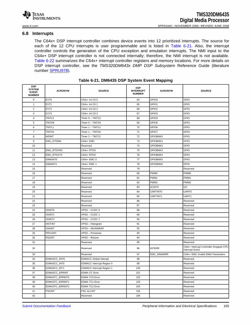
6.8 Interrupts
TMS320DM6435Digital Media Processor
www.ti.com SPRS344C–NOVEMBER 2006–REVISED JUNE 2008
The C64x+ DSP interrupt controller combines device events into 12 prioritized interrupts. The source foreach of the 12 CPU interrupts is user programmable and is listed in Table 6-21. Also, the interruptcontroller controls the generation of the CPU exception and emulation interrupts. The NMI input to theC64x+ DSP interrupt controller is not connected internally; therefore, the NMI interrupt is not available.Table 6-22 summarizes the C64x+ interrupt controller registers and memory locations. For more details onDSP interrupt controller, see the TMS320DM643x DMP DSP Subsystem Reference Guide (literaturenumber SPRU978).
Table 6-21. DM6435 DSP System Event MappingDSP DSPSYSTEM ACRONYM SOURCE INTERRUPT ACRONYM SOURCEEVENT NUMBERNUMBER
0 EVT0 C64x+ Int Ctl 0 64 GPIO0 GPIO
1 EVT1 C64x+ Int Ctl 1 65 GPIO1 GPIO
2 EVT2 C64x+ Int Ctl 2 66 GPIO2 GPIO
3 EVT3 C64x+ Int Ctl 3 67 GPIO3 GPIO
4 TINTL0 Timer 0 – TINT12 68 GPIO4 GPIO
5 TINTH0 Timer 0 – TINT34 69 GPIO5 GPIO
6 TINTL1 Timer 1 – TINT12 70 GPIO6 GPIO
7 TINTH1 Timer 1 – TINT34 71 GPIO7 GPIO
8 WDINT Timer 2 – TINT12 72 GPIOBNK0 GPIO
9 EMU_DTDMA C64x+ EMC 73 GPIOBNK1 GPIO
10 Reserved 74 GPIOBNK2 GPIO
11 EMU_RTDXRX C64x+ RTDX 75 GPIOBNK3 GPIO
12 EMU_RTDXTX C64x+ RTDX 76 GPIOBNK4 GPIO
13 IDMAINT0 C64x+ EMC 0 77 GPIOBNK5 GPIO
14 IDMAINT1 C64x+ EMC 1 78 GPIOBNK6 GPIO
15 Reserved 79 Reserved
16 Reserved 80 PWM0 PWM0
17 Reserved 81 PWM1 PWM1
18 Reserved 82 PWM2 PWM2
19 Reserved 83 IICINT0 I2C
20 Reserved 84 UARTINT0 UART0
21 Reserved 85 UARTINT1 UART1
22 Reserved 86 Reserved
23 Reserved 87 Reserved
24 VDINT0 VPSS – CCDC 0 88 Reserved
25 VDINT1 VPSS – CCDC 1 89 Reserved
26 VDINT2 VPSS – CCDC 2 90 Reserved
27 HISTINT VPSS – Histogram 91 Reserved
28 H3AINT VPSS – AE/AWB/AF 92 Reserved
29 PRVUINT VPSS – Previewer 93 Reserved
30 RSZINT VPSS – Resizer 94 Reserved
31 Reserved 95 Reserved
C64x+ Interrupt Controller Dropped CPU32 Reserved 96 INTERR Interrupt Event
33 Reserved 97 EMC_IDMAERR C64x+ EMC Invalid IDMA Parameters
34 EDMA3CC_INTG EDMACC Global Interupt 98 Reserved
35 EDMA3CC_INT0 EDMACC Interrupt Region 0 99 Reserved
36 EDMA3CC_INT1 EDMACC Interrupt Region 1 100 Reserved
37 EDMA3CC_ERRINT EDMA CC Error 101 Reserved
38 EDMA3TC_ERRINT0 EDMA TC0 Error 102 Reserved
39 EDMA3TC_ERRINT1 EDMA TC1 Error 103 Reserved
40 EDMA3TC_ERRINT2 EDMA TC2 Error 104 Reserved
41 PSCINT PSC ALLINT 105 Reserved
42 Reserved 106 Reserved
Submit Documentation Feedback Peripheral Information and Electrical Specifications 165
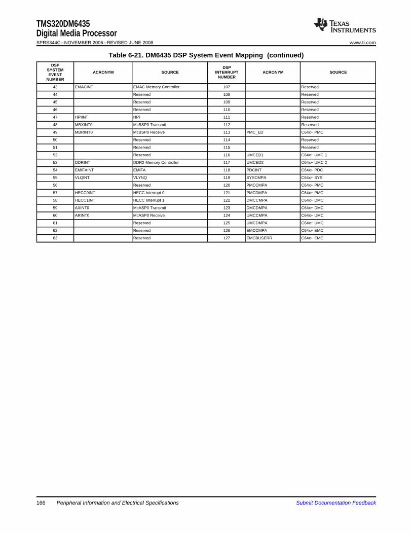
TMS320DM6435Digital Media ProcessorSPRS344C–NOVEMBER 2006–REVISED JUNE 2008 www.ti.com
Table 6-21. DM6435 DSP System Event Mapping (continued)DSP DSPSYSTEM ACRONYM SOURCE INTERRUPT ACRONYM SOURCEEVENT NUMBERNUMBER
43 EMACINT EMAC Memory Controller 107 Reserved
44 Reserved 108 Reserved
45 Reserved 109 Reserved
46 Reserved 110 Reserved
47 HPIINT HPI 111 Reserved
48 MBXINT0 McBSP0 Transmit 112 Reserved
49 MBRINT0 McBSP0 Receive 113 PMC_ED C64x+ PMC
50 Reserved 114 Reserved
51 Reserved 115 Reserved
52 Reserved 116 UMCED1 C64x+ UMC 1
53 DDRINT DDR2 Memory Controller 117 UMCED2 C64x+ UMC 2
54 EMIFAINT EMIFA 118 PDCINT C64x+ PDC
55 VLQINT VLYNQ 119 SYSCMPA C64x+ SYS
56 Reserved 120 PMCCMPA C64x+ PMC
57 HECC0INT HECC Interrupt 0 121 PMCDMPA C64x+ PMC
58 HECC1INT HECC Interrupt 1 122 DMCCMPA C64x+ DMC
59 AXINT0 McASP0 Transmit 123 DMCDMPA C64x+ DMC
60 ARINT0 McASP0 Receive 124 UMCCMPA C64x+ UMC
61 Reserved 125 UMCDMPA C64x+ UMC
62 Reserved 126 EMCCMPA C64x+ EMC
63 Reserved 127 EMCBUSERR C64x+ EMC
Peripheral Information and Electrical Specifications166 Submit Documentation Feedback
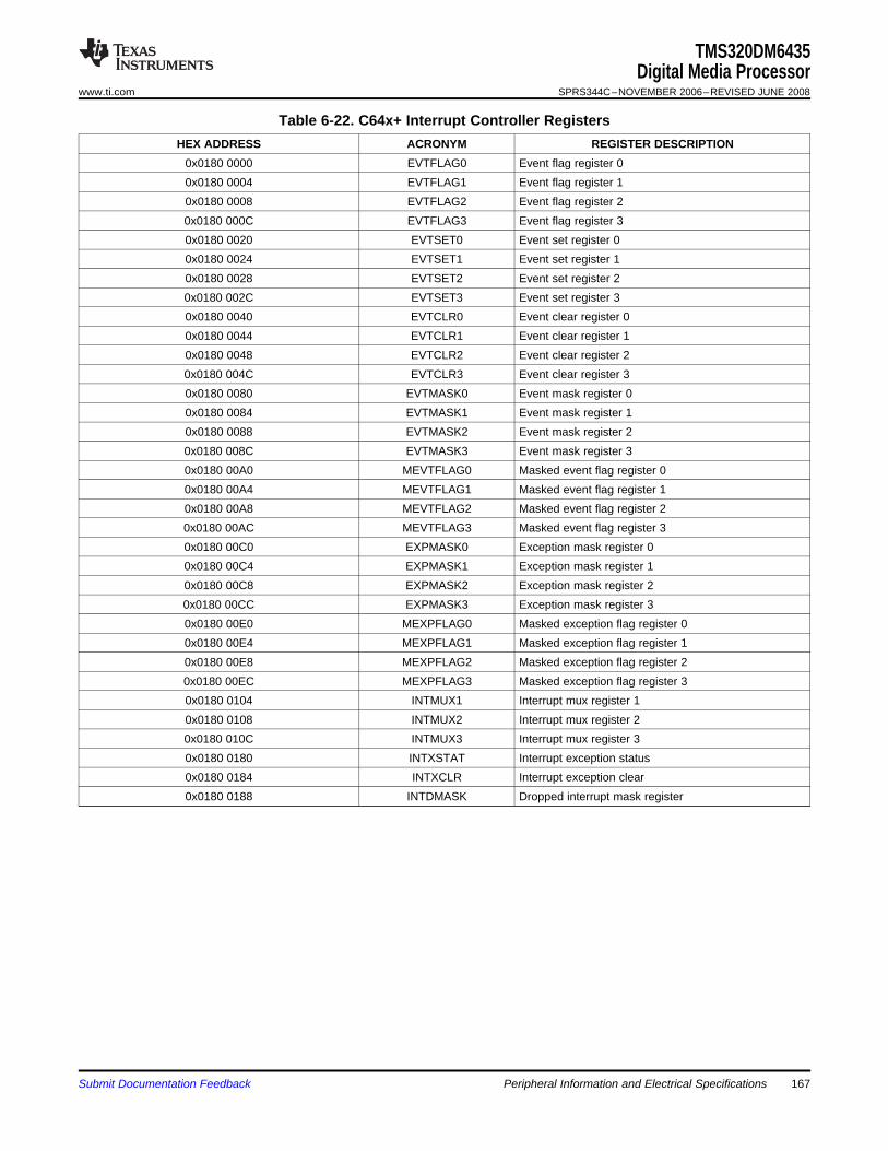
TMS320DM6435Digital Media Processor
www.ti.com SPRS344C–NOVEMBER 2006–REVISED JUNE 2008
Table 6-22. C64x+ Interrupt Controller RegistersHEX ADDRESS ACRONYM REGISTER DESCRIPTION
0x0180 0000 EVTFLAG0 Event flag register 00x0180 0004 EVTFLAG1 Event flag register 10x0180 0008 EVTFLAG2 Event flag register 20x0180 000C EVTFLAG3 Event flag register 30x0180 0020 EVTSET0 Event set register 00x0180 0024 EVTSET1 Event set register 10x0180 0028 EVTSET2 Event set register 20x0180 002C EVTSET3 Event set register 30x0180 0040 EVTCLR0 Event clear register 00x0180 0044 EVTCLR1 Event clear register 10x0180 0048 EVTCLR2 Event clear register 20x0180 004C EVTCLR3 Event clear register 30x0180 0080 EVTMASK0 Event mask register 00x0180 0084 EVTMASK1 Event mask register 10x0180 0088 EVTMASK2 Event mask register 20x0180 008C EVTMASK3 Event mask register 30x0180 00A0 MEVTFLAG0 Masked event flag register 00x0180 00A4 MEVTFLAG1 Masked event flag register 10x0180 00A8 MEVTFLAG2 Masked event flag register 20x0180 00AC MEVTFLAG3 Masked event flag register 30x0180 00C0 EXPMASK0 Exception mask register 00x0180 00C4 EXPMASK1 Exception mask register 10x0180 00C8 EXPMASK2 Exception mask register 20x0180 00CC EXPMASK3 Exception mask register 30x0180 00E0 MEXPFLAG0 Masked exception flag register 00x0180 00E4 MEXPFLAG1 Masked exception flag register 10x0180 00E8 MEXPFLAG2 Masked exception flag register 20x0180 00EC MEXPFLAG3 Masked exception flag register 30x0180 0104 INTMUX1 Interrupt mux register 10x0180 0108 INTMUX2 Interrupt mux register 20x0180 010C INTMUX3 Interrupt mux register 30x0180 0180 INTXSTAT Interrupt exception status0x0180 0184 INTXCLR Interrupt exception clear0x0180 0188 INTDMASK Dropped interrupt mask register
Submit Documentation Feedback Peripheral Information and Electrical Specifications 167
6.9 External Memory Interface (EMIF)
6.9.1 Asynchronous EMIF (EMIFA)
6.9.2 NAND (NAND, SmartMedia, xD)
TMS320DM6435Digital Media ProcessorSPRS344C–NOVEMBER 2006–REVISED JUNE 2008 www.ti.com
DM6435 supports several memory and external device interfaces, including:• Asynchronous EMIF (EMIFA) for interfacing to NOR Flash, SRAM, etc.• NAND Flash
The DM6435 Asynchronous EMIF (EMIFA) provides an 8-bit data bus, an address bus width up to 24-bits,and 4 chip selects, along with memory control signals. These signals are multiplexed between theseperipherals:• EMIFA and NAND interfaces• VPFE (CCDC)• GPIO
The EMIFA interface provides both the asynchronous EMIF and NAND interfaces. Four chip selects areprovided and each are individually configurable to provide either EMIFA or NAND support. The NANDfeatures supported are as follows.• NAND flash on up to 4 asynchronous chip selects.• 8-bit data bus width• Programmable cycle timings.• Performs ECC calculation.• NAND Mode also supports SmartMedia and xD memory cards• Boot ROM supports booting of the DM6435 from NAND flash located at CS2
The memory map for EMIFA and NAND registers is shown in Table 6-23. For more details on the EMIFAand NAND interfaces, see Section 2.9, Documentation Support for the link to the TMS320DM643x DMPPeripherals Overview Reference Guide (literature number SPRU983) for the TMS320DM643xAsynchronous External Memory Interface (EMIF) User's Guide (literature number SPRU984).
Peripheral Information and Electrical Specifications168 Submit Documentation Feedback
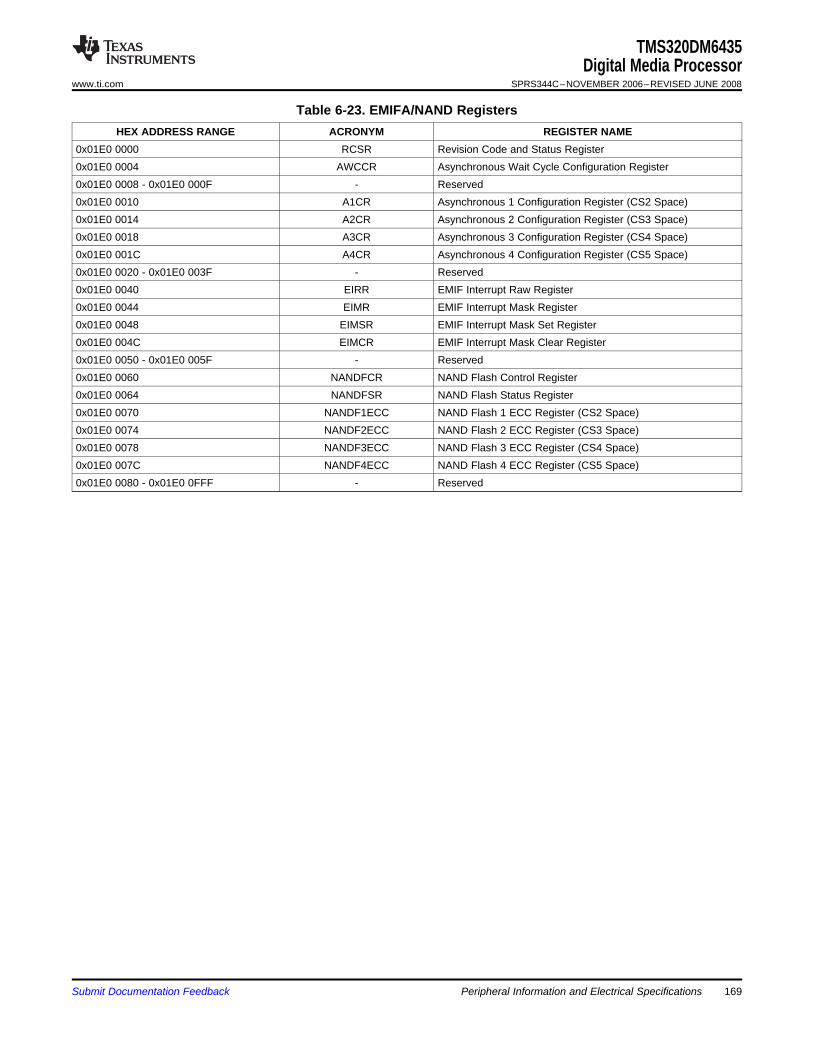
TMS320DM6435Digital Media Processor
www.ti.com SPRS344C–NOVEMBER 2006–REVISED JUNE 2008
Table 6-23. EMIFA/NAND RegistersHEX ADDRESS RANGE ACRONYM REGISTER NAME
0x01E0 0000 RCSR Revision Code and Status Register0x01E0 0004 AWCCR Asynchronous Wait Cycle Configuration Register0x01E0 0008 - 0x01E0 000F - Reserved0x01E0 0010 A1CR Asynchronous 1 Configuration Register (CS2 Space)0x01E0 0014 A2CR Asynchronous 2 Configuration Register (CS3 Space)0x01E0 0018 A3CR Asynchronous 3 Configuration Register (CS4 Space)0x01E0 001C A4CR Asynchronous 4 Configuration Register (CS5 Space)0x01E0 0020 - 0x01E0 003F - Reserved0x01E0 0040 EIRR EMIF Interrupt Raw Register0x01E0 0044 EIMR EMIF Interrupt Mask Register0x01E0 0048 EIMSR EMIF Interrupt Mask Set Register0x01E0 004C EIMCR EMIF Interrupt Mask Clear Register0x01E0 0050 - 0x01E0 005F - Reserved0x01E0 0060 NANDFCR NAND Flash Control Register0x01E0 0064 NANDFSR NAND Flash Status Register0x01E0 0070 NANDF1ECC NAND Flash 1 ECC Register (CS2 Space)0x01E0 0074 NANDF2ECC NAND Flash 2 ECC Register (CS3 Space)0x01E0 0078 NANDF3ECC NAND Flash 3 ECC Register (CS4 Space)0x01E0 007C NANDF4ECC NAND Flash 4 ECC Register (CS5 Space)0x01E0 0080 - 0x01E0 0FFF - Reserved
Submit Documentation Feedback Peripheral Information and Electrical Specifications 169
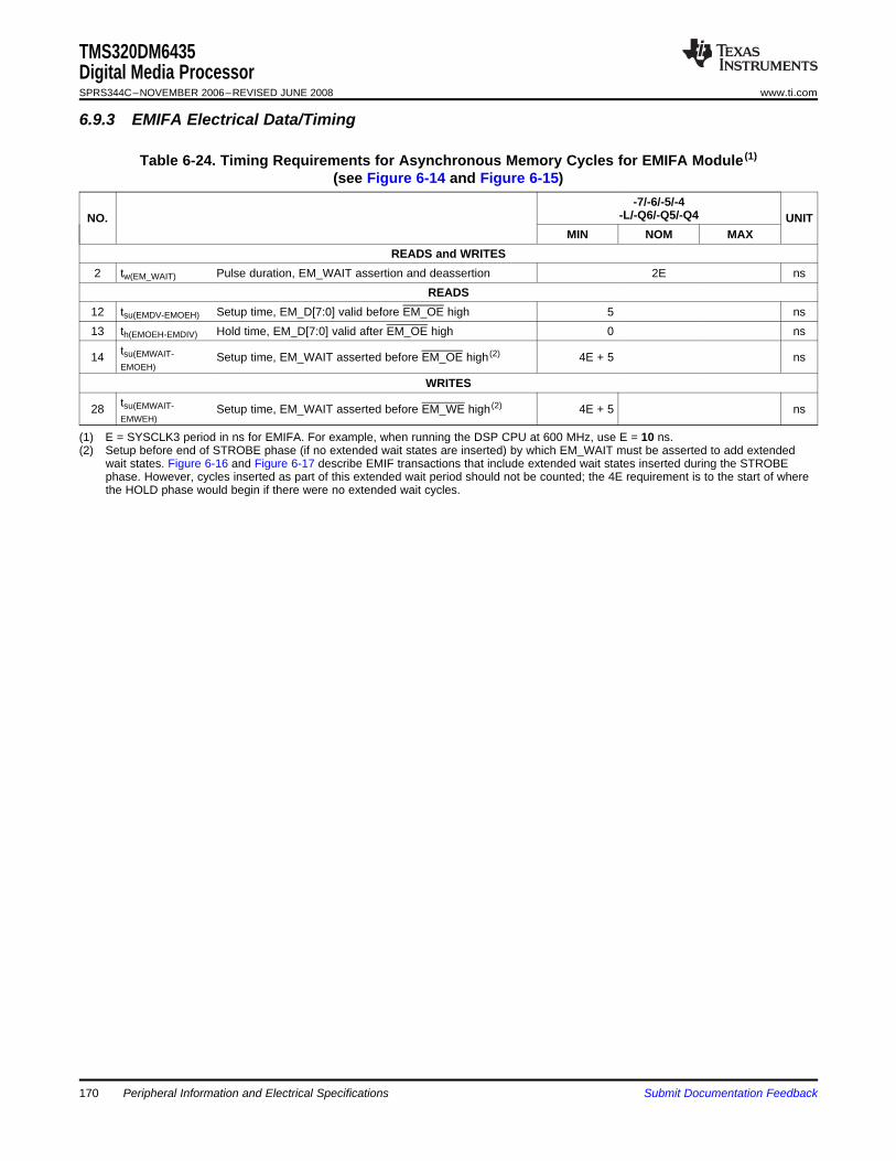
6.9.3 EMIFA Electrical Data/Timing
TMS320DM6435Digital Media ProcessorSPRS344C–NOVEMBER 2006–REVISED JUNE 2008 www.ti.com
Table 6-24. Timing Requirements for Asynchronous Memory Cycles for EMIFA Module (1)
(see Figure 6-14 and Figure 6-15)-7/-6/-5/-4
-L/-Q6/-Q5/-Q4NO. UNITMIN NOM MAX
READS and WRITES2 tw(EM_WAIT) Pulse duration, EM_WAIT assertion and deassertion 2E ns
READS12 tsu(EMDV-EMOEH) Setup time, EM_D[7:0] valid before EM_OE high 5 ns13 th(EMOEH-EMDIV) Hold time, EM_D[7:0] valid after EM_OE high 0 ns
tsu(EMWAIT-14 Setup time, EM_WAIT asserted before EM_OE high (2) 4E + 5 nsEMOEH)
WRITEStsu(EMWAIT-28 Setup time, EM_WAIT asserted before EM_WE high (2) 4E + 5 nsEMWEH)
(1) E = SYSCLK3 period in ns for EMIFA. For example, when running the DSP CPU at 600 MHz, use E = 10 ns.(2) Setup before end of STROBE phase (if no extended wait states are inserted) by which EM_WAIT must be asserted to add extended
wait states. Figure 6-16 and Figure 6-17 describe EMIF transactions that include extended wait states inserted during the STROBEphase. However, cycles inserted as part of this extended wait period should not be counted; the 4E requirement is to the start of wherethe HOLD phase would begin if there were no extended wait cycles.
Peripheral Information and Electrical Specifications170 Submit Documentation Feedback
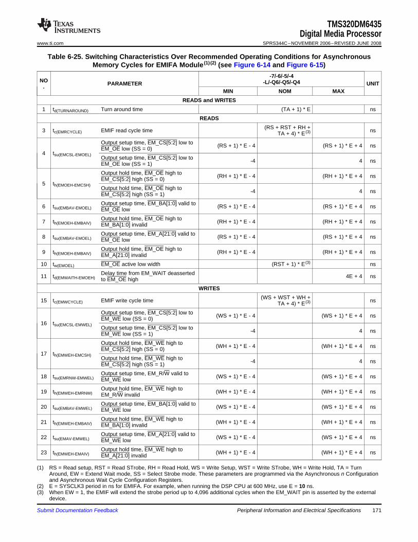
TMS320DM6435Digital Media Processor
www.ti.com SPRS344C–NOVEMBER 2006–REVISED JUNE 2008
Table 6-25. Switching Characteristics Over Recommended Operating Conditions for AsynchronousMemory Cycles for EMIFA Module (1) (2) (see Figure 6-14 and Figure 6-15)
-7/-6/-5/-4NO -L/-Q6/-Q5/-Q4PARAMETER UNIT.
MIN NOM MAXREADS and WRITES
1 td(TURNAROUND) Turn around time (TA + 1) * E nsREADS
(RS + RST + RH +3 tc(EMRCYCLE) EMIF read cycle time nsTA + 4) * E (3)
Output setup time, EM_CS[5:2] low to (RS + 1) * E - 4 (RS + 1) * E + 4 nsEM_OE low (SS = 0)4 tsu(EMCSL-EMOEL) Output setup time, EM_CS[5:2] low to -4 4 nsEM_OE low (SS = 1)
Output hold time, EM_OE high to (RH + 1) * E - 4 (RH + 1) * E + 4 nsEM_CS[5:2] high (SS = 0)5 th(EMOEH-EMCSH) Output hold time, EM_OE high to -4 4 nsEM_CS[5:2] high (SS = 1)
Output setup time, EM_BA[1:0] valid to6 tsu(EMBAV-EMOEL) (RS + 1) * E - 4 (RS + 1) * E + 4 nsEM_OE lowOutput hold time, EM_OE high to7 th(EMOEH-EMBAIV) (RH + 1) * E - 4 (RH + 1) * E + 4 nsEM_BA[1:0] invalidOutput setup time, EM_A[21:0] valid to8 tsu(EMBAV-EMOEL) (RS + 1) * E - 4 (RS + 1) * E + 4 nsEM_OE lowOutput hold time, EM_OE high to9 th(EMOEH-EMBAIV) (RH + 1) * E - 4 (RH + 1) * E + 4 nsEM_A[21:0] invalid
10 tw(EMOEL) EM_OE active low width (RST + 1) * E (3) nsDelay time from EM_WAIT deasserted11 td(EMWAITH-EMOEH) 4E + 4 nsto EM_OE high
WRITES(WS + WST + WH +15 tc(EMWCYCLE) EMIF write cycle time nsTA + 4) * E (3)
Output setup time, EM_CS[5:2] low to (WS + 1) * E - 4 (WS + 1) * E + 4 nsEM_WE low (SS = 0)16 tsu(EMCSL-EMWEL) Output setup time, EM_CS[5:2] low to -4 4 nsEM_WE low (SS = 1)
Output hold time, EM_WE high to (WH + 1) * E - 4 (WH + 1) * E + 4 nsEM_CS[5:2] high (SS = 0)17 th(EMWEH-EMCSH) Output hold time, EM_WE high to -4 4 nsEM_CS[5:2] high (SS = 1)
Output setup time, EM_R/W valid to18 tsu(EMRNW-EMWEL) (WS + 1) * E - 4 (WS + 1) * E + 4 nsEM_WE lowOutput hold time, EM_WE high to19 th(EMWEH-EMRNW) (WH + 1) * E - 4 (WH + 1) * E + 4 nsEM_R/W invalidOutput setup time, EM_BA[1:0] valid to20 tsu(EMBAV-EMWEL) (WS + 1) * E - 4 (WS + 1) * E + 4 nsEM_WE lowOutput hold time, EM_WE high to21 th(EMWEH-EMBAIV) (WH + 1) * E - 4 (WH + 1) * E + 4 nsEM_BA[1:0] invalidOutput setup time, EM_A[21:0] valid to22 tsu(EMAV-EMWEL) (WS + 1) * E - 4 (WS + 1) * E + 4 nsEM_WE lowOutput hold time, EM_WE high to23 th(EMWEH-EMAIV) (WH + 1) * E - 4 (WH + 1) * E + 4 nsEM_A[21:0] invalid
(1) RS = Read setup, RST = Read STrobe, RH = Read Hold, WS = Write Setup, WST = Write STrobe, WH = Write Hold, TA = TurnAround, EW = Extend Wait mode, SS = Select Strobe mode. These parameters are programmed via the Asynchronous n Configurationand Asynchronous Wait Cycle Configuration Registers.
(2) E = SYSCLK3 period in ns for EMIFA. For example, when running the DSP CPU at 600 MHz, use E = 10 ns.(3) When EW = 1, the EMIF will extend the strobe period up to 4,096 additional cycles when the EM_WAIT pin is asserted by the external
device.
Submit Documentation Feedback Peripheral Information and Electrical Specifications 171
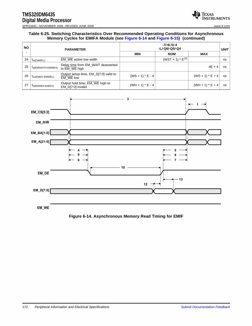
EM_CS[5:2]
EM_BA[1:0]
13
12
EM_A[21:0]
EM_OE
EM_D[7:0]
EM_WE
10
5
9
7
4
8
6
3
1
EM_R/W
TMS320DM6435Digital Media ProcessorSPRS344C–NOVEMBER 2006–REVISED JUNE 2008 www.ti.com
Table 6-25. Switching Characteristics Over Recommended Operating Conditions for AsynchronousMemory Cycles for EMIFA Module (see Figure 6-14 and Figure 6-15) (continued)
-7/-6/-5/-4NO -L/-Q6/-Q5/-Q4PARAMETER UNIT.
MIN NOM MAX24 tw(EMWEL) EM_WE active low width (WST + 1) * E (3) ns
Delay time from EM_WAIT deasserted25 td(EMWAITH-EMWEH) 4E + 4 nsto EM_WE highOutput setup time, EM_D[7:0] valid to26 tsu(EMDV-EMWEL) (WS + 1) * E - 4 (WS + 1) * E + 4 nsEM_WE lowOutput hold time, EM_WE high to27 th(EMWEH-EMDIV) (WH + 1) * E - 4 (WH + 1) * E + 4 nsEM_D[7:0] invalid
Figure 6-14. Asynchronous Memory Read Timing for EMIF
172 Peripheral Information and Electrical Specifications Submit Documentation Feedback

EM_CS[5:2]
EM_BA[1:0]
EM_A[21:0]
EM_WE
EM_D[7:0]
EM_OE
EM_R/W
15
1
16
18
20
2224
17
19
21
23
26
27
EM_CS[5:2]
11
Asserted Deasserted
22
EM_BA[1:0]
EM_A[21:0]
EM_D[7:0]
EM_OE
EM_WAIT
SETUP STROBE Extended Due to EM_WAIT STROBE HOLD
14
TMS320DM6435Digital Media Processor
www.ti.com SPRS344C–NOVEMBER 2006–REVISED JUNE 2008
Figure 6-15. Asynchronous Memory Write Timing for EMIF
Figure 6-16. EM_WAIT Read Timing Requirements
Submit Documentation Feedback Peripheral Information and Electrical Specifications 173
EM_CS[5:2]
25
Asserted Deasserted
22
EM_BA[1:0]
EM_A[21:0]
EM_D[7:0]
EM_WE
EM_WAIT
SETUP STROBE Extended Due to EM_WAIT STROBE HOLD
28
6.9.4 DDR2 Memory Controller
TMS320DM6435Digital Media ProcessorSPRS344C–NOVEMBER 2006–REVISED JUNE 2008 www.ti.com
Figure 6-17. EM_WAIT Write Timing Requirements
The DDR2 Memory Controller is a dedicated interface to DDR2 SDRAM. It supports JESD79D-2Astandard compliant DDR2 SDRAM Devices and can interface to either 16-bit or 32-bit DDR2 SDRAMdevices. For details on the DDR2 Memory Controller, see Section 2.9, Document Support for the link tothe TMS320DM643x DMP Peripherals Overview Reference Guide (literature number SPRU983) for theTMS320C642x/DM643x DMP DDR2 Memory Controller User's Guide (literature number SPRU986).
DDR2 SDRAM plays a key role in a DaVinci-based system. Such a system is expected to require asignificant amount of high-speed external memory for:• Buffering of input image data from sensors or video sources• Intermediate buffering for processing/resizing of image data in the VPFE• Intermediate buffering for large raw Bayer data image files while performing image processing
functions• Buffering for intermediate data while performing video encode and decode functions• Storage of executable code for the DSP
A memory map of the DDR2 Memory Controller registers is shown in Table 6-26.
Table 6-26. DDR2 Memory Controller RegistersHEX ADDRESS RANGE ACRONYM REGISTER NAME
0x01C4 004C DDRVTPER DDR2 VTP Enable Register0x01C4 2038 DDRVTPR DDR2 VTP Register0x2000 0000 - 0x2000 0003 - Reserved0x2000 0004 SDRSTAT SDRAM Status Register0x2000 0008 SDBCR SDRAM Bank Configuration Register0x2000 000C SDRCR SDRAM Refresh Control Register0x2000 0010 SDTIMR SDRAM Timing Register0x2000 0014 SDTIMR2 SDRAM Timing Register 20x2000 0020 PBBPR Peripheral Bus Burst Priority Register0x2000 0024 - 0x2000 00BF - Reserved0x2000 00C0 IRR Interrupt Raw Register0x2000 00C4 IMR Interrupt Masked Register0x2000 00C8 IMSR Interrupt Mask Set Register0x2000 00CC IMCR Interrupt Mask Clear Register
Peripheral Information and Electrical Specifications174 Submit Documentation Feedback
6.9.4.1 DDR2 Memory Controller Electrical Data/Timing
DDR_CLK
1
TMS320DM6435Digital Media Processor
www.ti.com SPRS344C–NOVEMBER 2006–REVISED JUNE 2008
Table 6-26. DDR2 Memory Controller Registers (continued)HEX ADDRESS RANGE ACRONYM REGISTER NAME
0x2000 00D0 - 0x2000 00E3 - Reserved0x2000 00E4 DDRPHYCR DDR PHY Control Register0x2000 00E8 - 0x2000 00EF - Reserved0x2000 00F0 VTPIOCR DDR VTP IO Control Register0x2000 00F4 - 0x2000 7FFF - Reserved
The Implementing DDR2 PCB Layout on the TMS320DM643x DMP DMSoC Application Report (literaturenumber SPRAAL6) specifies a complete DDR2 interface solution for the DM6435 as well as a list ofcompatible DDR2 devices. TI has performed the simulation and system characterization to ensure allDDR2 interface timings in this solution are met.
TI only supports board designs that follow the guidelines outlined in the Implementing DDR2 PCB Layouton the TMS320DM643x DMP DMSoC Application Report (literature number SPRAAL6).
Table 6-27. Switching Characteristics Over Recommended Operating Conditions for DDR2 MemoryController (1) (2)(see Figure 6-18)
-7/-6/-5/-4-L/-Q6/-Q5/-Q4NO. PARAMETER UNIT
MIN MAX1 tc(DDR_CLK) Cycle time, DDR_CLK 6 8 ns
(1) DDR_CLK cycle time = 2 x PLL2 _SYSCLK1 cycle time.(2) The PLL2 Controller must be programmed such that the resulting DDR_CLK clock frequency is within the specified range.
Figure 6-18. DDR2 Memory Controller Clock Timing
Submit Documentation Feedback Peripheral Information and Electrical Specifications 175
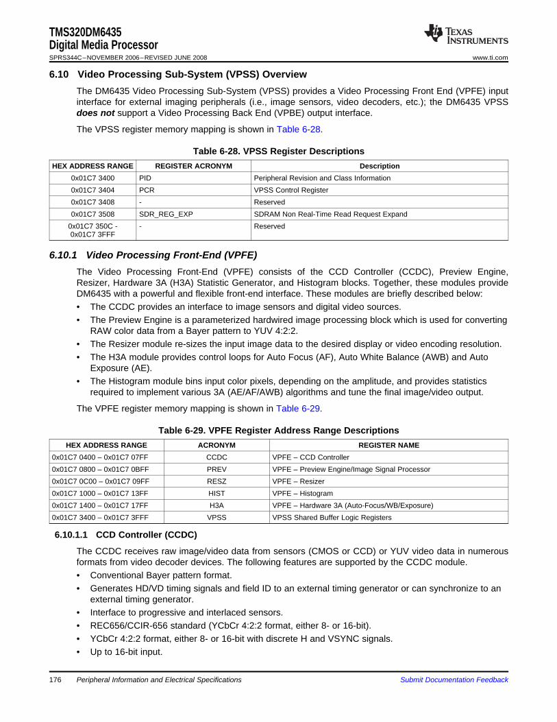
6.10 Video Processing Sub-System (VPSS) Overview
6.10.1 Video Processing Front-End (VPFE)
6.10.1.1 CCD Controller (CCDC)
TMS320DM6435Digital Media ProcessorSPRS344C–NOVEMBER 2006–REVISED JUNE 2008 www.ti.com
The DM6435 Video Processing Sub-System (VPSS) provides a Video Processing Front End (VPFE) inputinterface for external imaging peripherals (i.e., image sensors, video decoders, etc.); the DM6435 VPSSdoes not support a Video Processing Back End (VPBE) output interface.
The VPSS register memory mapping is shown in Table 6-28.
Table 6-28. VPSS Register DescriptionsHEX ADDRESS RANGE REGISTER ACRONYM Description
0x01C7 3400 PID Peripheral Revision and Class Information0x01C7 3404 PCR VPSS Control Register0x01C7 3408 - Reserved0x01C7 3508 SDR_REG_EXP SDRAM Non Real-Time Read Request Expand
0x01C7 350C - - Reserved0x01C7 3FFF
The Video Processing Front-End (VPFE) consists of the CCD Controller (CCDC), Preview Engine,Resizer, Hardware 3A (H3A) Statistic Generator, and Histogram blocks. Together, these modules provideDM6435 with a powerful and flexible front-end interface. These modules are briefly described below:• The CCDC provides an interface to image sensors and digital video sources.• The Preview Engine is a parameterized hardwired image processing block which is used for converting
RAW color data from a Bayer pattern to YUV 4:2:2.• The Resizer module re-sizes the input image data to the desired display or video encoding resolution.• The H3A module provides control loops for Auto Focus (AF), Auto White Balance (AWB) and Auto
Exposure (AE).• The Histogram module bins input color pixels, depending on the amplitude, and provides statistics
required to implement various 3A (AE/AF/AWB) algorithms and tune the final image/video output.
The VPFE register memory mapping is shown in Table 6-29.
Table 6-29. VPFE Register Address Range DescriptionsHEX ADDRESS RANGE ACRONYM REGISTER NAME
0x01C7 0400 – 0x01C7 07FF CCDC VPFE – CCD Controller0x01C7 0800 – 0x01C7 0BFF PREV VPFE – Preview Engine/Image Signal Processor0x01C7 0C00 – 0x01C7 09FF RESZ VPFE – Resizer0x01C7 1000 – 0x01C7 13FF HIST VPFE – Histogram0x01C7 1400 – 0x01C7 17FF H3A VPFE – Hardware 3A (Auto-Focus/WB/Exposure)0x01C7 3400 – 0x01C7 3FFF VPSS VPSS Shared Buffer Logic Registers
The CCDC receives raw image/video data from sensors (CMOS or CCD) or YUV video data in numerousformats from video decoder devices. The following features are supported by the CCDC module.• Conventional Bayer pattern format.• Generates HD/VD timing signals and field ID to an external timing generator or can synchronize to an
external timing generator.• Interface to progressive and interlaced sensors.• REC656/CCIR-656 standard (YCbCr 4:2:2 format, either 8- or 16-bit).• YCbCr 4:2:2 format, either 8- or 16-bit with discrete H and VSYNC signals.• Up to 16-bit input.
Peripheral Information and Electrical Specifications176 Submit Documentation Feedback
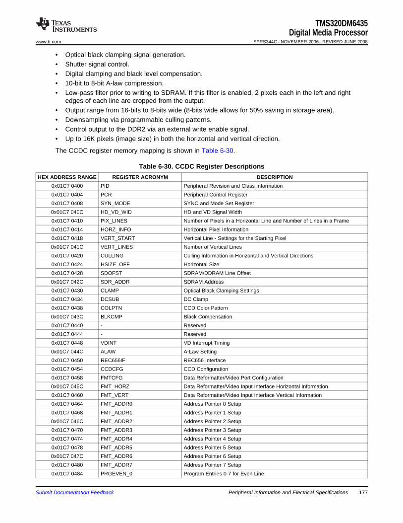
TMS320DM6435Digital Media Processor
www.ti.com SPRS344C–NOVEMBER 2006–REVISED JUNE 2008
• Optical black clamping signal generation.• Shutter signal control.• Digital clamping and black level compensation.• 10-bit to 8-bit A-law compression.• Low-pass filter prior to writing to SDRAM. If this filter is enabled, 2 pixels each in the left and right
edges of each line are cropped from the output.• Output range from 16-bits to 8-bits wide (8-bits wide allows for 50% saving in storage area).• Downsampling via programmable culling patterns.• Control output to the DDR2 via an external write enable signal.• Up to 16K pixels (image size) in both the horizontal and vertical direction.
The CCDC register memory mapping is shown in Table 6-30.
Table 6-30. CCDC Register DescriptionsHEX ADDRESS RANGE REGISTER ACRONYM DESCRIPTION
0x01C7 0400 PID Peripheral Revision and Class Information0x01C7 0404 PCR Peripheral Control Register0x01C7 0408 SYN_MODE SYNC and Mode Set Register0x01C7 040C HD_VD_WID HD and VD Signal Width0x01C7 0410 PIX_LINES Number of Pixels in a Horizontal Line and Number of Lines in a Frame0x01C7 0414 HORZ_INFO Horizontal Pixel Information0x01C7 0418 VERT_START Vertical Line - Settings for the Starting Pixel0x01C7 041C VERT_LINES Number of Vertical Lines0x01C7 0420 CULLING Culling Information in Horizontal and Vertical Directions0x01C7 0424 HSIZE_OFF Horizontal Size0x01C7 0428 SDOFST SDRAM/DDRAM Line Offset0x01C7 042C SDR_ADDR SDRAM Address0x01C7 0430 CLAMP Optical Black Clamping Settings0x01C7 0434 DCSUB DC Clamp0x01C7 0438 COLPTN CCD Color Pattern0x01C7 043C BLKCMP Black Compensation0x01C7 0440 - Reserved0x01C7 0444 - Reserved0x01C7 0448 VDINT VD Interrupt Timing0x01C7 044C ALAW A-Law Setting0x01C7 0450 REC656IF REC656 Interface0x01C7 0454 CCDCFG CCD Configuration0x01C7 0458 FMTCFG Data Reformatter/Video Port Configuration0x01C7 045C FMT_HORZ Data Reformatter/Video Input Interface Horizontal Information0x01C7 0460 FMT_VERT Data Reformatter/Video Input Interface Vertical Information0x01C7 0464 FMT_ADDR0 Address Pointer 0 Setup0x01C7 0468 FMT_ADDR1 Address Pointer 1 Setup0x01C7 046C FMT_ADDR2 Address Pointer 2 Setup0x01C7 0470 FMT_ADDR3 Address Pointer 3 Setup0x01C7 0474 FMT_ADDR4 Address Pointer 4 Setup0x01C7 0478 FMT_ADDR5 Address Pointer 5 Setup0x01C7 047C FMT_ADDR6 Address Pointer 6 Setup0x01C7 0480 FMT_ADDR7 Address Pointer 7 Setup0x01C7 0484 PRGEVEN_0 Program Entries 0-7 for Even Line
Submit Documentation Feedback Peripheral Information and Electrical Specifications 177
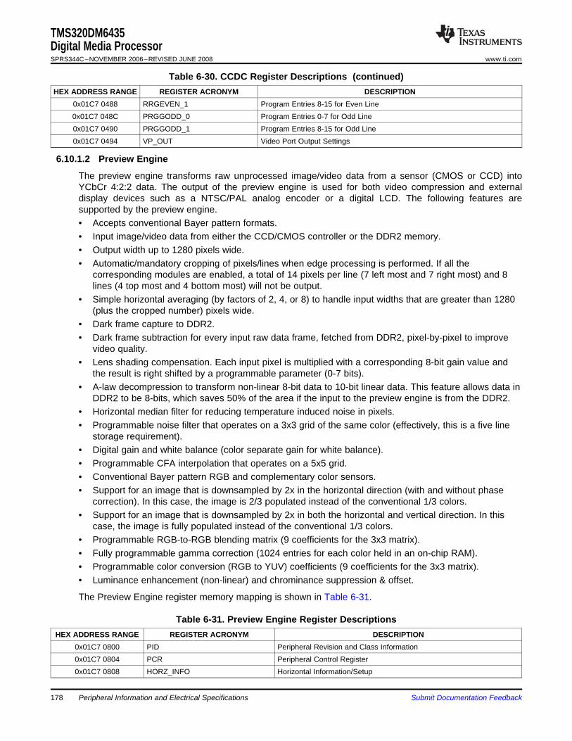
6.10.1.2 Preview Engine
TMS320DM6435Digital Media ProcessorSPRS344C–NOVEMBER 2006–REVISED JUNE 2008 www.ti.com
Table 6-30. CCDC Register Descriptions (continued)HEX ADDRESS RANGE REGISTER ACRONYM DESCRIPTION
0x01C7 0488 RRGEVEN_1 Program Entries 8-15 for Even Line0x01C7 048C PRGGODD_0 Program Entries 0-7 for Odd Line0x01C7 0490 PRGGODD_1 Program Entries 8-15 for Odd Line0x01C7 0494 VP_OUT Video Port Output Settings
The preview engine transforms raw unprocessed image/video data from a sensor (CMOS or CCD) intoYCbCr 4:2:2 data. The output of the preview engine is used for both video compression and externaldisplay devices such as a NTSC/PAL analog encoder or a digital LCD. The following features aresupported by the preview engine.• Accepts conventional Bayer pattern formats.• Input image/video data from either the CCD/CMOS controller or the DDR2 memory.• Output width up to 1280 pixels wide.• Automatic/mandatory cropping of pixels/lines when edge processing is performed. If all the
corresponding modules are enabled, a total of 14 pixels per line (7 left most and 7 right most) and 8lines (4 top most and 4 bottom most) will not be output.
• Simple horizontal averaging (by factors of 2, 4, or 8) to handle input widths that are greater than 1280(plus the cropped number) pixels wide.
• Dark frame capture to DDR2.• Dark frame subtraction for every input raw data frame, fetched from DDR2, pixel-by-pixel to improve
video quality.• Lens shading compensation. Each input pixel is multiplied with a corresponding 8-bit gain value and
the result is right shifted by a programmable parameter (0-7 bits).• A-law decompression to transform non-linear 8-bit data to 10-bit linear data. This feature allows data in
DDR2 to be 8-bits, which saves 50% of the area if the input to the preview engine is from the DDR2.• Horizontal median filter for reducing temperature induced noise in pixels.• Programmable noise filter that operates on a 3x3 grid of the same color (effectively, this is a five line
storage requirement).• Digital gain and white balance (color separate gain for white balance).• Programmable CFA interpolation that operates on a 5x5 grid.• Conventional Bayer pattern RGB and complementary color sensors.• Support for an image that is downsampled by 2x in the horizontal direction (with and without phase
correction). In this case, the image is 2/3 populated instead of the conventional 1/3 colors.• Support for an image that is downsampled by 2x in both the horizontal and vertical direction. In this
case, the image is fully populated instead of the conventional 1/3 colors.• Programmable RGB-to-RGB blending matrix (9 coefficients for the 3x3 matrix).• Fully programmable gamma correction (1024 entries for each color held in an on-chip RAM).• Programmable color conversion (RGB to YUV) coefficients (9 coefficients for the 3x3 matrix).• Luminance enhancement (non-linear) and chrominance suppression & offset.
The Preview Engine register memory mapping is shown in Table 6-31.
Table 6-31. Preview Engine Register DescriptionsHEX ADDRESS RANGE REGISTER ACRONYM DESCRIPTION
0x01C7 0800 PID Peripheral Revision and Class Information0x01C7 0804 PCR Peripheral Control Register0x01C7 0808 HORZ_INFO Horizontal Information/Setup
Peripheral Information and Electrical Specifications178 Submit Documentation Feedback
6.10.1.3 Resizer
TMS320DM6435Digital Media Processor
www.ti.com SPRS344C–NOVEMBER 2006–REVISED JUNE 2008
Table 6-31. Preview Engine Register Descriptions (continued)HEX ADDRESS RANGE REGISTER ACRONYM DESCRIPTION
0x01C7 080C VERT_INFO Vertical Information/Setup0x01C7 0810 RSDR_ADDR Read Address From SDRAM0x01C7 0814 RADR_OFFSET Line Offset for the Read Data0x01C7 0818 DSDR_ADDR Dark Frame Address From SDRAM0x01C7 081C DRKF_OFFSET Line Offset for the Dark Frame Data0x01C7 0820 WSDR_ADDR Write Address to the SDRAM0x01C7 0824 WADD_OFFSET Line Offset for the Write Data0x01C7 0828 AVE Input Formatter/Averager0x01C7 082C HMED Horizontal Median Filter0x01C7 0830 NF Noise Filter0x01C7 0834 WB_DGAIN White Balance Digital Gain0x01C7 0838 WBGAIN White Balance Coefficients0x01C7 083C WBSEL White Balance Coefficients Selection0x01C7 0840 CFA CFA Register0x01C7 0844 BLKADJOFF Black Adjustment Offset0x01C7 0848 RGB_MAT1 RGB2RGB Blending Matrix Coefficients0x01C7 084C RGB_MAT2 RGB2RGB Blending Matrix Coefficients0x01C7 0850 RGB_MAT3 RGB2RGB Blending Matrix Coefficients0x01C7 0854 RGB_MAT4 RGB2RGB Blending Matrix Coefficients0x01C7 0858 RGB_MAT5 RGB2RGB Blending Matrix Coefficients0x01C7 085C RGB_OFF1 RGB2RGB Blending Matrix Offsets0x01C7 0860 RGB_OFF2 RGB2RGB Blending Matrix Offsets0x01C7 0864 CSC0 Color Space Conversion Coefficients0x01C7 0868 CSC1 Color Space Conversion Coefficients0x01C7 086C CSC2 Color Space Conversion Coefficients0x01C7 0870 CSC_OFFSET Color Space Conversion Offsets0x01C7 0874 CNT_BRT Contrast and Brightness Settings0x01C7 0878 CSUP Chrominance Suppression Settings0x01C7 087C SETUP_YC Maximum/Minimum Y and C Settings0x01C7 0880 SET_TBL_ADDRESS Setup Table Addresses0x01C7 0884 SET_TBL_DATA Setup Table Data
The resizer module can accept input image/video data from either the preview engine or DDR2. Theoutput of the resizer module is sent to DDR2. The following features are supported by the resizer module.• An output width up to 1280 horizontal pixels.• Input from external DDR2.• Up to 4x upsampling (digital zoom).• Bi-cubic interpolation (4-tap horizontal, 4-tap vertical) can be implemented with the programmable filter
coefficients.• 8 phases of filter coefficients.• Optional bi-linear interpolation for the chrominance components.• Up to 1/4x downsampling• 4-tap horizontal and 4-tap vertical filter coefficients (with 8-phases) for 1x to 1/2x downsampling• 1/2x to 1/4x downsampling, for 7-tap mode with 4-phases.• Resizing either YUV 4:2:2 packed data (16-bits) or color separate data (8-bit data within DDR) that is
contiguous.
Submit Documentation Feedback Peripheral Information and Electrical Specifications 179
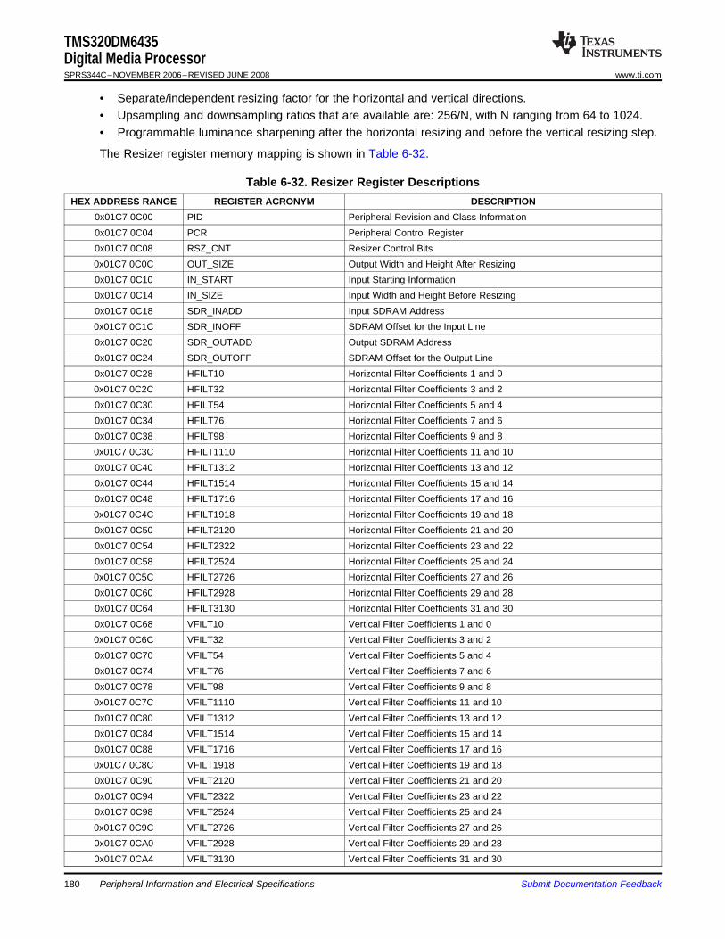
TMS320DM6435Digital Media ProcessorSPRS344C–NOVEMBER 2006–REVISED JUNE 2008 www.ti.com
• Separate/independent resizing factor for the horizontal and vertical directions.• Upsampling and downsampling ratios that are available are: 256/N, with N ranging from 64 to 1024.• Programmable luminance sharpening after the horizontal resizing and before the vertical resizing step.
The Resizer register memory mapping is shown in Table 6-32.
Table 6-32. Resizer Register DescriptionsHEX ADDRESS RANGE REGISTER ACRONYM DESCRIPTION
0x01C7 0C00 PID Peripheral Revision and Class Information0x01C7 0C04 PCR Peripheral Control Register0x01C7 0C08 RSZ_CNT Resizer Control Bits0x01C7 0C0C OUT_SIZE Output Width and Height After Resizing0x01C7 0C10 IN_START Input Starting Information0x01C7 0C14 IN_SIZE Input Width and Height Before Resizing0x01C7 0C18 SDR_INADD Input SDRAM Address0x01C7 0C1C SDR_INOFF SDRAM Offset for the Input Line0x01C7 0C20 SDR_OUTADD Output SDRAM Address0x01C7 0C24 SDR_OUTOFF SDRAM Offset for the Output Line0x01C7 0C28 HFILT10 Horizontal Filter Coefficients 1 and 00x01C7 0C2C HFILT32 Horizontal Filter Coefficients 3 and 20x01C7 0C30 HFILT54 Horizontal Filter Coefficients 5 and 40x01C7 0C34 HFILT76 Horizontal Filter Coefficients 7 and 60x01C7 0C38 HFILT98 Horizontal Filter Coefficients 9 and 80x01C7 0C3C HFILT1110 Horizontal Filter Coefficients 11 and 100x01C7 0C40 HFILT1312 Horizontal Filter Coefficients 13 and 120x01C7 0C44 HFILT1514 Horizontal Filter Coefficients 15 and 140x01C7 0C48 HFILT1716 Horizontal Filter Coefficients 17 and 160x01C7 0C4C HFILT1918 Horizontal Filter Coefficients 19 and 180x01C7 0C50 HFILT2120 Horizontal Filter Coefficients 21 and 200x01C7 0C54 HFILT2322 Horizontal Filter Coefficients 23 and 220x01C7 0C58 HFILT2524 Horizontal Filter Coefficients 25 and 240x01C7 0C5C HFILT2726 Horizontal Filter Coefficients 27 and 260x01C7 0C60 HFILT2928 Horizontal Filter Coefficients 29 and 280x01C7 0C64 HFILT3130 Horizontal Filter Coefficients 31 and 300x01C7 0C68 VFILT10 Vertical Filter Coefficients 1 and 00x01C7 0C6C VFILT32 Vertical Filter Coefficients 3 and 20x01C7 0C70 VFILT54 Vertical Filter Coefficients 5 and 40x01C7 0C74 VFILT76 Vertical Filter Coefficients 7 and 60x01C7 0C78 VFILT98 Vertical Filter Coefficients 9 and 80x01C7 0C7C VFILT1110 Vertical Filter Coefficients 11 and 100x01C7 0C80 VFILT1312 Vertical Filter Coefficients 13 and 120x01C7 0C84 VFILT1514 Vertical Filter Coefficients 15 and 140x01C7 0C88 VFILT1716 Vertical Filter Coefficients 17 and 160x01C7 0C8C VFILT1918 Vertical Filter Coefficients 19 and 180x01C7 0C90 VFILT2120 Vertical Filter Coefficients 21 and 200x01C7 0C94 VFILT2322 Vertical Filter Coefficients 23 and 220x01C7 0C98 VFILT2524 Vertical Filter Coefficients 25 and 240x01C7 0C9C VFILT2726 Vertical Filter Coefficients 27 and 260x01C7 0CA0 VFILT2928 Vertical Filter Coefficients 29 and 280x01C7 0CA4 VFILT3130 Vertical Filter Coefficients 31 and 30
Peripheral Information and Electrical Specifications180 Submit Documentation Feedback
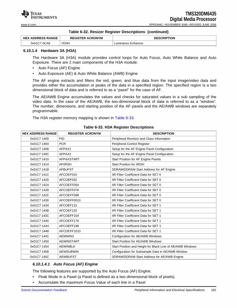
6.10.1.4 Hardware 3A (H3A)
TMS320DM6435Digital Media Processor
www.ti.com SPRS344C–NOVEMBER 2006–REVISED JUNE 2008
Table 6-32. Resizer Register Descriptions (continued)HEX ADDRESS RANGE REGISTER ACRONYM DESCRIPTION
0x01C7 0CA8 YENH Luminance Enhancer
The Hardware 3A (H3A) module provides control loops for Auto Focus, Auto White Balance and AutoExposure. There are 2 main components of the H3A module:• Auto Focus (AF) Engine• Auto Exposure (AE) & Auto White Balance (AWB) Engine
The AF engine extracts and filters the red, green, and blue data from the input image/video data andprovides either the accumulation or peaks of the data in a specified region. The specified region is a twodimensional block of data and is referred to as a “paxel” for the case of AF.
The AE/AWB Engine accumulates the values and checks for saturated values in a sub sampling of thevideo data. In the case of the AE/AWB, the two-dimensional block of data is referred to as a “window”.The number, dimensions, and starting position of the AF paxels and the AE/AWB windows are separatelyprogrammable.
The H3A register memory mapping is shown in Table 6-33.
Table 6-33. H3A Register DescriptionsHEX ADDRESS RANGE REGISTER ACRONYM DESCRIPTION
0x01C7 1400 PID Peripheral Revision and Class Information0x01C7 1404 PCR Peripheral Control Register0x01C7 1408 AFPAX1 Setup for the AF Engine Paxel Configuration0x01C7 140C AFPAX2 Setup for the AF Engine Paxel Configuration0x01C7 1410 AFPAXSTART Start Position for AF Engine Paxels0x01C7 1414 AFIIRSH Start Position for IIRSH0x01C7 1418 AFBUFST SDRAM/DDRAM Start Address for AF Engine0x01C7 141C AFCOEF010 IIR Filter Coefficient Data for SET 00x01C7 1420 AFCOEF032 IIR Filter Coefficient Data for SET 00x01C7 1424 AFCOEFF054 IIR Filter Coefficient Data for SET 00x01C7 1428 AFCOEFF076 IIR Filter Coefficient Data for SET 00x01C7 142C AFCOEFF098 IIR Filter Coefficient Data for SET 00x01C7 1430 AFCOEFF0010 IIR Filter Coefficient Data for SET 00x01C7 1434 AFCOEF110 IIR Filter Coefficient Data for SET 10x01C7 1438 AFCOEF132 IIR Filter Coefficient Data for SET 10x01C7 143C AFCOEFF154 IIR Filter Coefficient Data for SET 10x01C7 1440 AFCOEFF176 IIR Filter Coefficient Data for SET 10x01C7 1444 AFCOEFF198 IIR Filter Coefficient Data for SET 10x01C7 1448 AFCOEFF1010 IIR Filter Coefficient Data for SET 10x01C7 144C AEWWIN1 Configuration for AE/AWB Windows0x01C7 1450 AEWINSTART Start Position for AE/AWB Windows0x01C7 1454 AEWINBLK Start Position and Height for Black Line of AE/AWB Windows0x01C7 1458 AEWSUBWIN Configuration for Subsample Data in AE/AWB Window0x01C7 145C AEWBUFST SDRAM/DDRAM Start Address for AE/AWB Engine
6.10.1.4.1 Auto Focus (AF) Engine
The following features are supported by the Auto Focus (AF) Engine.• Peak Mode in a Paxel (a Paxel is defined as a two dimensional block of pixels).• Accumulate the maximum Focus Value of each line in a Paxel
Submit Documentation Feedback Peripheral Information and Electrical Specifications 181
6.10.1.5 Histogram
TMS320DM6435Digital Media ProcessorSPRS344C–NOVEMBER 2006–REVISED JUNE 2008 www.ti.com
• Accumulation/Sum Mode (instead of Peak mode).• Accumulate Focus Value in a Paxel.• Up to 36 Paxels in the horizontal direction and up to 128 Paxels in the vertical direction.• Programmable width and height for the Paxel. All paxels in the frame will be of same size.• Programmable red, green, and blue position within a 2x2 matrix.• Separate horizontal start for paxel and filtering.• Programmable vertical line increments within a paxel.• Parallel IIR filters configured in a dual-biquad configuration with individual coefficients (2 filters with 11
coefficients each). The filters are intended to compute the sharpness/peaks in the frame to focus on.6.10.1.4.2 Auto Exposure (AE) and Auto White Balance (AWB) Engine
The following features are supported by the Auto Exposure (AE) and Auto White Balance (AWB) Engine.• Accumulate clipped pixels along with all non-saturated pixels.• Up to 36 horizontal windows.• Up to 128 vertical windows.• Programmable width and height for the windows. All windows in the frame will be of same size.• Separate vertical start coordinate and height for a black row of paxels that is different than the
remaining color paxels.• Programmable Horizontal Sampling Points in a window.• Programmable Vertical Sampling Points in a window.
The histogram module accepts raw image/video data and bins the pixels on a value (and color separate)basis. The value of the pixel itself is not stored, but each bin contains the number of pixels that are withinthe appropriate set range. The source of the raw data for the histogram is typically a CCD/CMOS sensor(via the CCDC module) or optionally from DDR2. The following features are supported by the histogrammodule.• Up to four regions/areas.• Separate horizontal/vertical start and end position for each region.• Pixels from overlapping regions are accumulated into the highest priority region. The priority is: region0
> region1 > region2 > region3.• Interface to conventional Bayer pattern. Each region can accumulate either 3 or 4 colors.• 32, 64, 128, or 256 bins per color per region.• 32, 64, or 128 bins per color for 2 regions.• 32 or 64 bins per color for 3 or 4 regions.• Automatic clear of histogram RAM after an ARM read.• Saturation of the pixel count if the count exceeds the maximum value (each memory location is 20-bit
wide).• Downshift ranging from 0 to 7 bits (maximum bin range 128).• The last bin (highest range of values) will accumulate any value that is higher than the lower bound.
The Histogram register memory mapping is shown in Table 6-34.
Table 6-34. Histogram Register DescriptionsHEX ADDRESS RANGE REGISTER ACRONYM DESCRIPTION
0x01C7 1000 PID Peripheral Revision and Class Information Register0x01C7 1004 PCR Peripheral Control Register0x01C7 1008 HIST_CNT Histogram Control Bits Register0x01C7 100C WB_GAIN White/Channel Balance Settings Register
Peripheral Information and Electrical Specifications182 Submit Documentation Feedback
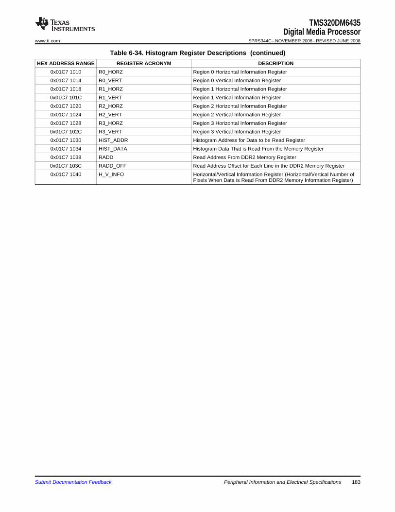
TMS320DM6435Digital Media Processor
www.ti.com SPRS344C–NOVEMBER 2006–REVISED JUNE 2008
Table 6-34. Histogram Register Descriptions (continued)HEX ADDRESS RANGE REGISTER ACRONYM DESCRIPTION
0x01C7 1010 R0_HORZ Region 0 Horizontal Information Register0x01C7 1014 R0_VERT Region 0 Vertical Information Register0x01C7 1018 R1_HORZ Region 1 Horizontal Information Register0x01C7 101C R1_VERT Region 1 Vertical Information Register0x01C7 1020 R2_HORZ Region 2 Horizontal Information Register0x01C7 1024 R2_VERT Region 2 Vertical Information Register0x01C7 1028 R3_HORZ Region 3 Horizontal Information Register0x01C7 102C R3_VERT Region 3 Vertical Information Register0x01C7 1030 HIST_ADDR Histogram Address for Data to be Read Register0x01C7 1034 HIST_DATA Histogram Data That is Read From the Memory Register0x01C7 1038 RADD Read Address From DDR2 Memory Register0x01C7 103C RADD_OFF Read Address Offset for Each Line in the DDR2 Memory Register0x01C7 1040 H_V_INFO Horizontal/Vertical Information Register (Horizontal/Vertical Number of
Pixels When Data is Read From DDR2 Memory Information Register)
Submit Documentation Feedback Peripheral Information and Electrical Specifications 183
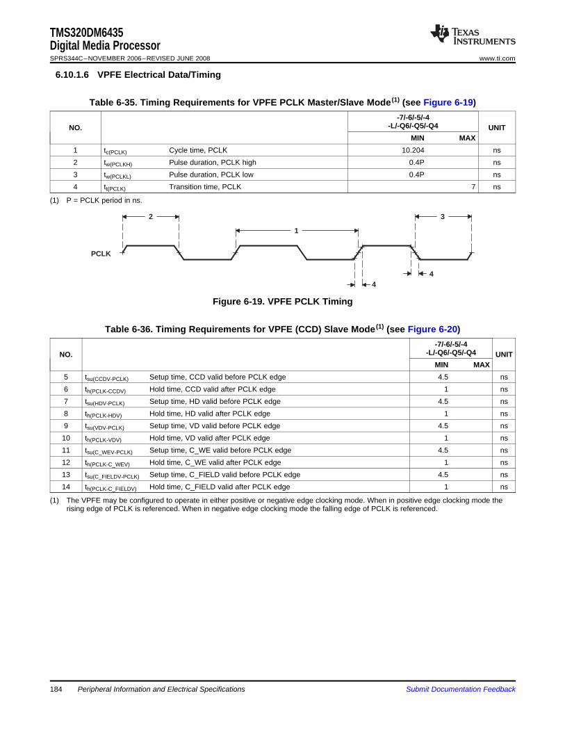
6.10.1.6 VPFE Electrical Data/Timing
PCLK
2
1
3
44
TMS320DM6435Digital Media ProcessorSPRS344C–NOVEMBER 2006–REVISED JUNE 2008 www.ti.com
Table 6-35. Timing Requirements for VPFE PCLK Master/Slave Mode (1) (see Figure 6-19)-7/-6/-5/-4
-L/-Q6/-Q5/-Q4NO. UNITMIN MAX
1 tc(PCLK) Cycle time, PCLK 10.204 ns2 tw(PCLKH) Pulse duration, PCLK high 0.4P ns3 tw(PCLKL) Pulse duration, PCLK low 0.4P ns4 tt(PCLK) Transition time, PCLK 7 ns
(1) P = PCLK period in ns.
Figure 6-19. VPFE PCLK Timing
Table 6-36. Timing Requirements for VPFE (CCD) Slave Mode (1) (see Figure 6-20)-7/-6/-5/-4
-L/-Q6/-Q5/-Q4NO. UNITMIN MAX
5 tsu(CCDV-PCLK) Setup time, CCD valid before PCLK edge 4.5 ns6 th(PCLK-CCDV) Hold time, CCD valid after PCLK edge 1 ns7 tsu(HDV-PCLK) Setup time, HD valid before PCLK edge 4.5 ns8 th(PCLK-HDV) Hold time, HD valid after PCLK edge 1 ns9 tsu(VDV-PCLK) Setup time, VD valid before PCLK edge 4.5 ns10 th(PCLK-VDV) Hold time, VD valid after PCLK edge 1 ns11 tsu(C_WEV-PCLK) Setup time, C_WE valid before PCLK edge 4.5 ns12 th(PCLK-C_WEV) Hold time, C_WE valid after PCLK edge 1 ns13 tsu(C_FIELDV-PCLK) Setup time, C_FIELD valid before PCLK edge 4.5 ns14 th(PCLK-C_FIELDV) Hold time, C_FIELD valid after PCLK edge 1 ns
(1) The VPFE may be configured to operate in either positive or negative edge clocking mode. When in positive edge clocking mode therising edge of PCLK is referenced. When in negative edge clocking mode the falling edge of PCLK is referenced.
Peripheral Information and Electrical Specifications184 Submit Documentation Feedback
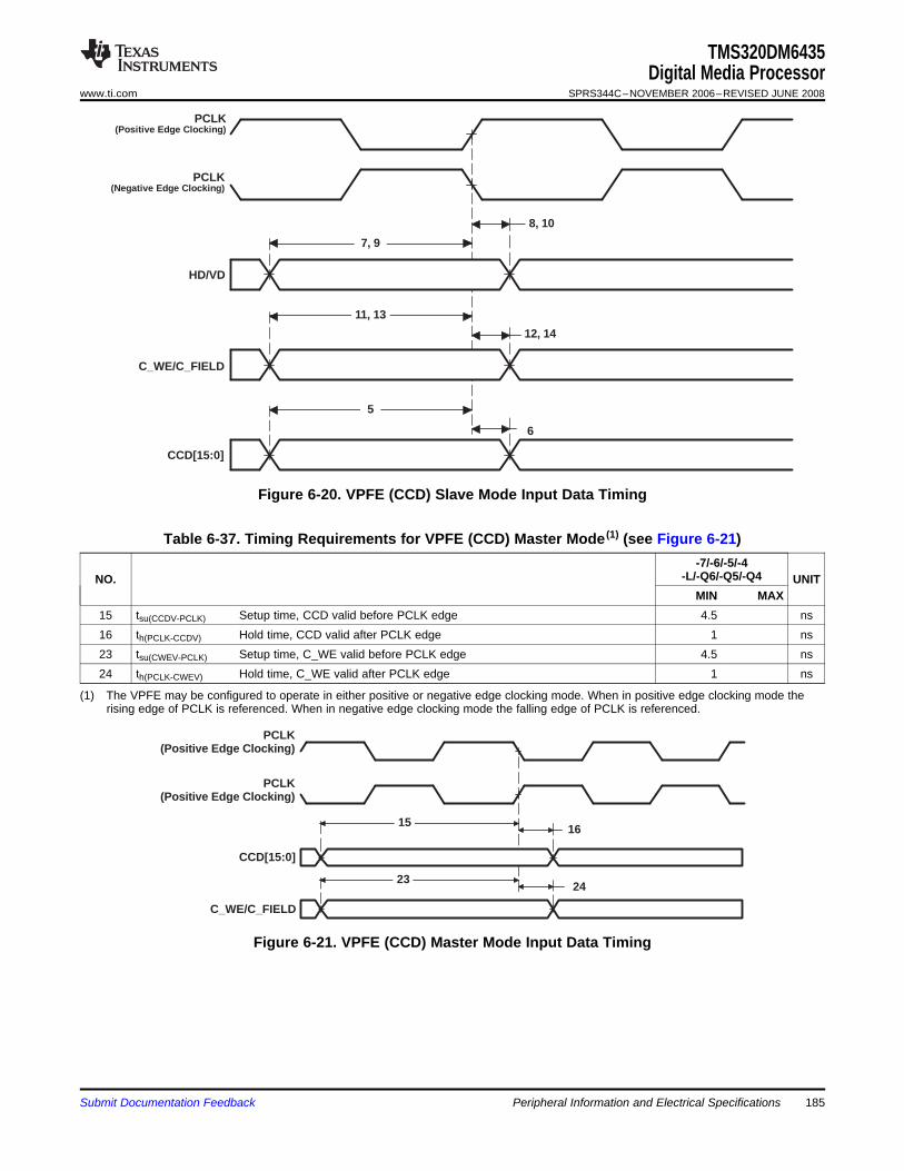
PCLK(Positive Edge Clocking)
PCLK(Negative Edge Clocking)
7, 9
HD/VD
CCD[15:0]
8, 10
11, 13
12, 14
5
6
C_WE/C_FIELD
PCLK(Positive Edge Clocking)
1516
2324
CCD[15:0]
C_WE/C_FIELD
PCLK(Positive Edge Clocking)
TMS320DM6435Digital Media Processor
www.ti.com SPRS344C–NOVEMBER 2006–REVISED JUNE 2008
Figure 6-20. VPFE (CCD) Slave Mode Input Data Timing
Table 6-37. Timing Requirements for VPFE (CCD) Master Mode (1) (see Figure 6-21)-7/-6/-5/-4
-L/-Q6/-Q5/-Q4NO. UNITMIN MAX
15 tsu(CCDV-PCLK) Setup time, CCD valid before PCLK edge 4.5 ns16 th(PCLK-CCDV) Hold time, CCD valid after PCLK edge 1 ns23 tsu(CWEV-PCLK) Setup time, C_WE valid before PCLK edge 4.5 ns24 th(PCLK-CWEV) Hold time, C_WE valid after PCLK edge 1 ns
(1) The VPFE may be configured to operate in either positive or negative edge clocking mode. When in positive edge clocking mode therising edge of PCLK is referenced. When in negative edge clocking mode the falling edge of PCLK is referenced.
Figure 6-21. VPFE (CCD) Master Mode Input Data Timing
Submit Documentation Feedback Peripheral Information and Electrical Specifications 185
PCLK
18
20
22
HD
VD
C_FIELD
TMS320DM6435Digital Media ProcessorSPRS344C–NOVEMBER 2006–REVISED JUNE 2008 www.ti.com
Table 6-38. Switching Characteristics Over Recommended Operating Conditions for VPFE (CCD) MasterMode (1) (see Figure 6-22)
-7/-6/-5/-4-L/-Q6/-Q5/-Q4NO. PARAMETER UNIT
MIN MAX18 td(PCLK-HDV) Delay time, PCLK edge to HD valid 2 9.5 ns20 td(PCLK-VDV) Delay time, PCLK edge to VD valid 2 9.5 ns22 td(PCLK-C_FIELDV) Delay time, PCLK edge to C_FIELD valid 2 9.5 ns
(1) The VPFE may be configured to operate in either positive or negative edge clocking mode. When in positive edge clocking mode therising edge of PCLK is referenced. When in negative edge clocking mode the falling edge of PCLK is referenced.
Figure 6-22. VPFE (CCD) Master Mode Control Output Data Timing
186 Peripheral Information and Electrical Specifications Submit Documentation Feedback
6.11 Universal Asynchronous Receiver/Transmitter (UART)
6.11.1 UART Peripheral Register Description(s)
TMS320DM6435Digital Media Processor
www.ti.com SPRS344C–NOVEMBER 2006–REVISED JUNE 2008
DM6435 has 2 UART peripherals. Each UART has the following features:• 16-byte storage space for both the transmitter and receiver FIFOs• 1, 4, 8, or 14 byte selectable receiver FIFO trigger level for autoflow control and DMA• DMA signaling capability for both received and transmitted data• Programmable auto-rts and auto-cts for autoflow control• Frequency pre-scale values from 1 to 65,535 to generate appropriate baud rates• Prioritized interrupts• Programmable serial data formats
– 5, 6, 7, or 8-bit characters– Even, odd, or no parity bit generation and detection– 1, 1.5, or 2 stop bit generation
• False start bit detection• Line break generation and detection• Internal diagnostic capabilities
– Loopback controls for communications link fault isolation– Break, parity, overrun, and framing error simulation
• Modem control functions (CTS, RTS) on UART0 only.
The UART0/1 registers are listed in Table 6-39 and Table 6-40 .
Table 6-39. UART0 Register DescriptionsHEX ADDRESS RANGE ACRONYM REGISTER NAME0x01C2 0000 RBR UART0 Receiver Buffer Register (Read Only)0x01C2 0000 THR UART0 Transmitter Holding Register (Write Only)0x01C2 0004 IER UART0 Interrupt Enable Register0x01C2 0008 IIR UART0 Interrupt Identification Register (Read Only)0x01C2 0008 FCR UART0 FIFO Control Register (Write Only)0x01C2 000C LCR UART0 Line Control Register0x01C2 0010 MCR UART0 Modem Control Register0x01C2 0014 LSR UART0 Line Status Register0x01C2 0018 - Reserved0x01C2 001C - Reserved0x01C2 0020 DLL UART0 Divisor Latch (LSB)0x01C2 0024 DLH UART0 Divisor Latch (MSB)0x01C2 0028 PID1 Peripheral Identification Register 10x01C2 002C PID2 Peripheral Identification Register 20x01C2 0030 PWREMU_MGMT UART0 Power and Emulation Management Register0x01C2 0034 - 0x01C2 03FF - Reserved
Table 6-40. UART1 Register DescriptionsHEX ADDRESS RANGE ACRONYM REGISTER NAME0x01C2 0400 RBR UART1 Receiver Buffer Register (Read Only)0x01C2 0400 THR UART1 Transmitter Holding Register (Write Only)0x01C2 0404 IER UART1 Interrupt Enable Register
Submit Documentation Feedback Peripheral Information and Electrical Specifications 187
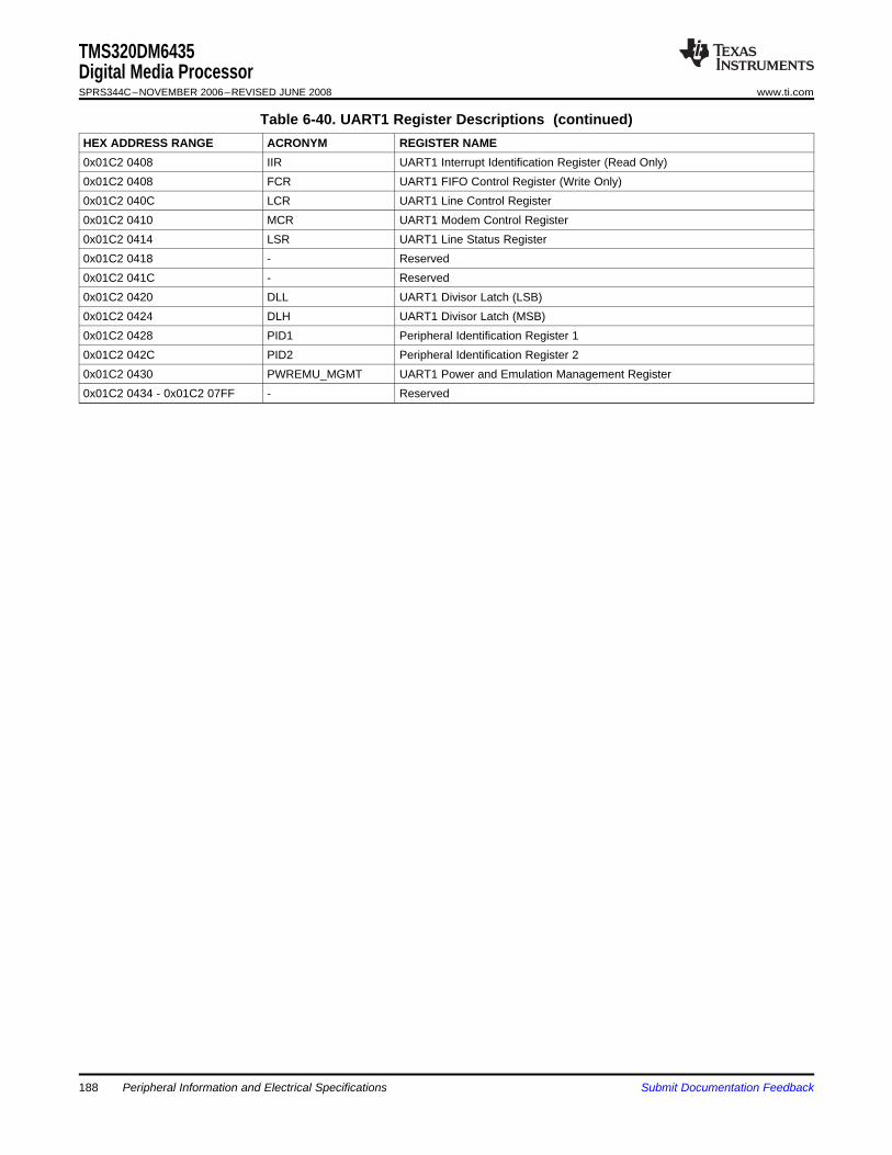
TMS320DM6435Digital Media ProcessorSPRS344C–NOVEMBER 2006–REVISED JUNE 2008 www.ti.com
Table 6-40. UART1 Register Descriptions (continued)HEX ADDRESS RANGE ACRONYM REGISTER NAME0x01C2 0408 IIR UART1 Interrupt Identification Register (Read Only)0x01C2 0408 FCR UART1 FIFO Control Register (Write Only)0x01C2 040C LCR UART1 Line Control Register0x01C2 0410 MCR UART1 Modem Control Register0x01C2 0414 LSR UART1 Line Status Register0x01C2 0418 - Reserved0x01C2 041C - Reserved0x01C2 0420 DLL UART1 Divisor Latch (LSB)0x01C2 0424 DLH UART1 Divisor Latch (MSB)0x01C2 0428 PID1 Peripheral Identification Register 10x01C2 042C PID2 Peripheral Identification Register 20x01C2 0430 PWREMU_MGMT UART1 Power and Emulation Management Register0x01C2 0434 - 0x01C2 07FF - Reserved
Peripheral Information and Electrical Specifications188 Submit Documentation Feedback
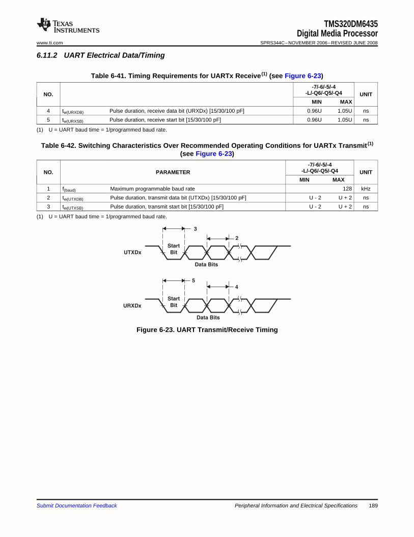
6.11.2 UART Electrical Data/Timing
3
2
Start
Bit
Data Bits
UTXDx
5
Data Bits
Bit
Start
4
URXDx
TMS320DM6435Digital Media Processor
www.ti.com SPRS344C–NOVEMBER 2006–REVISED JUNE 2008
Table 6-41. Timing Requirements for UARTx Receive (1) (see Figure 6-23)-7/-6/-5/-4
-L/-Q6/-Q5/-Q4NO. UNITMIN MAX
4 tw(URXDB) Pulse duration, receive data bit (URXDx) [15/30/100 pF] 0.96U 1.05U ns5 tw(URXSB) Pulse duration, receive start bit [15/30/100 pF] 0.96U 1.05U ns
(1) U = UART baud time = 1/programmed baud rate.
Table 6-42. Switching Characteristics Over Recommended Operating Conditions for UARTx Transmit (1)
(see Figure 6-23)-7/-6/-5/-4
-L/-Q6/-Q5/-Q4NO. PARAMETER UNITMIN MAX
1 f(baud) Maximum programmable baud rate 128 kHz2 tw(UTXDB) Pulse duration, transmit data bit (UTXDx) [15/30/100 pF] U - 2 U + 2 ns3 tw(UTXSB) Pulse duration, transmit start bit [15/30/100 pF] U - 2 U + 2 ns
(1) U = UART baud time = 1/programmed baud rate.
Figure 6-23. UART Transmit/Receive Timing
Submit Documentation Feedback Peripheral Information and Electrical Specifications 189
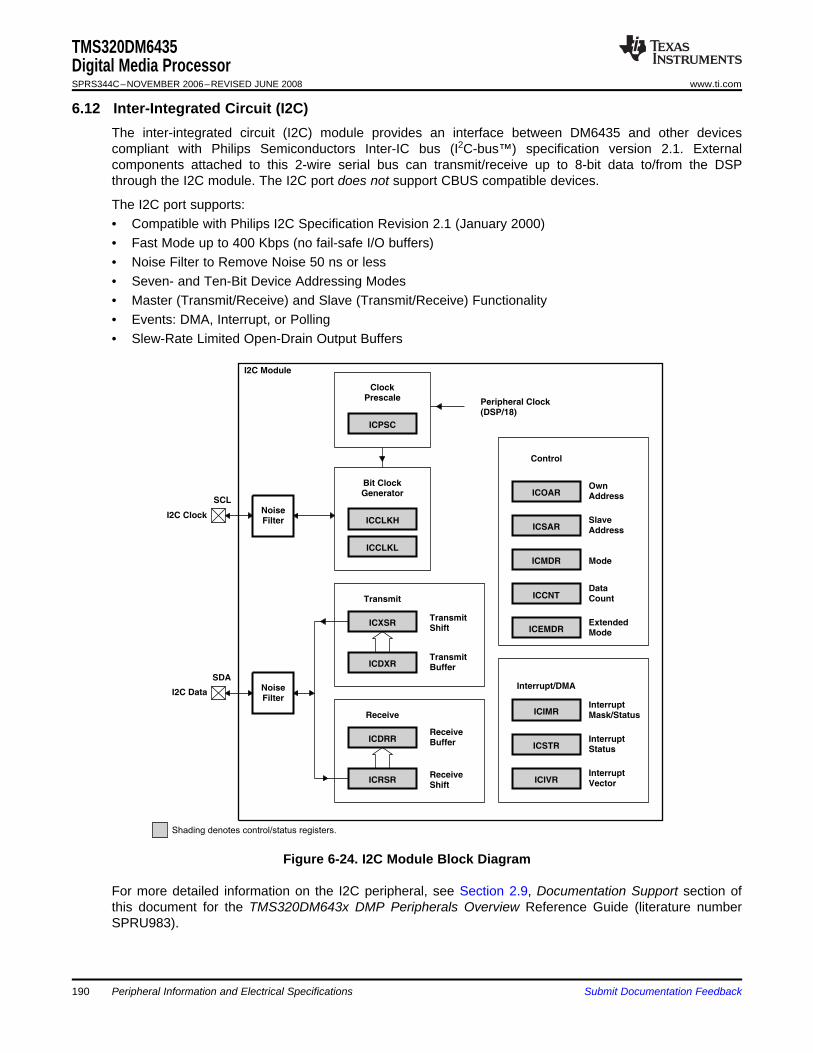
6.12 Inter-Integrated Circuit (I2C)
Clock
Prescale
ICPSC
Peripheral Clock
(DSP/18)
ICCLKH
Generator
Bit Clock
ICCLKL
Noise
Filter
SCL
ICXSR
ICDXR
Transmit
Transmit
Shift
Transmit
Buffer
ICDRR
ShiftICRSR
Receive
Buffer
Receive
Receive
Filter
SDA
I2C DataNoise
ICOAR
ICSARSlave
Address
Control
Address
Own
ICMDR
ICCNT
Mode
Data
Count
Vector
Interrupt
Interrupt
Status
ICIVR
ICSTR
Mask/Status
InterruptICIMR
Interrupt/DMA
I2C Module
I2C Clock
Shading denotes control/status registers.
ICEMDRExtended
Mode
TMS320DM6435Digital Media ProcessorSPRS344C–NOVEMBER 2006–REVISED JUNE 2008 www.ti.com
The inter-integrated circuit (I2C) module provides an interface between DM6435 and other devicescompliant with Philips Semiconductors Inter-IC bus (I2C-bus™) specification version 2.1. Externalcomponents attached to this 2-wire serial bus can transmit/receive up to 8-bit data to/from the DSPthrough the I2C module. The I2C port does not support CBUS compatible devices.
The I2C port supports:• Compatible with Philips I2C Specification Revision 2.1 (January 2000)• Fast Mode up to 400 Kbps (no fail-safe I/O buffers)• Noise Filter to Remove Noise 50 ns or less• Seven- and Ten-Bit Device Addressing Modes• Master (Transmit/Receive) and Slave (Transmit/Receive) Functionality• Events: DMA, Interrupt, or Polling• Slew-Rate Limited Open-Drain Output Buffers
Figure 6-24. I2C Module Block Diagram
For more detailed information on the I2C peripheral, see Section 2.9, Documentation Support section ofthis document for the TMS320DM643x DMP Peripherals Overview Reference Guide (literature numberSPRU983).
Peripheral Information and Electrical Specifications190 Submit Documentation Feedback
6.12.1 I2C Peripheral Register Description(s)
TMS320DM6435Digital Media Processor
www.ti.com SPRS344C–NOVEMBER 2006–REVISED JUNE 2008
Table 6-43. I2C RegistersHEX ADDRESS RANGE ACRONYM REGISTER NAME
0x1C2 1000 ICOAR I2C Own Address Register0x1C2 1004 ICIMR I2C Interrupt Mask Register0x1C2 1008 ICSTR I2C Interrupt Status Register0x1C2 100C ICCLKL I2C Clock Divider Low Register0x1C2 1010 ICCLKH I2C Clock Divider High Register0x1C2 1014 ICCNT I2C Data Count Register0x1C2 1018 ICDRR I2C Data Receive Register0x1C2 101C ICSAR I2C Slave Address Register0x1C2 1020 ICDXR I2C Data Transmit Register0x1C2 1024 ICMDR I2C Mode Register0x1C2 1028 ICIVR I2C Interrupt Vector Register0x1C2 102C ICEMDR I2C Extended Mode Register0x1C2 1030 ICPSC I2C Prescaler Register0x1C2 1034 ICPID1 I2C Peripheral Identification Register 10x1C2 1038 ICPID2 I2C Peripheral Identification Register 2
Submit Documentation Feedback Peripheral Information and Electrical Specifications 191
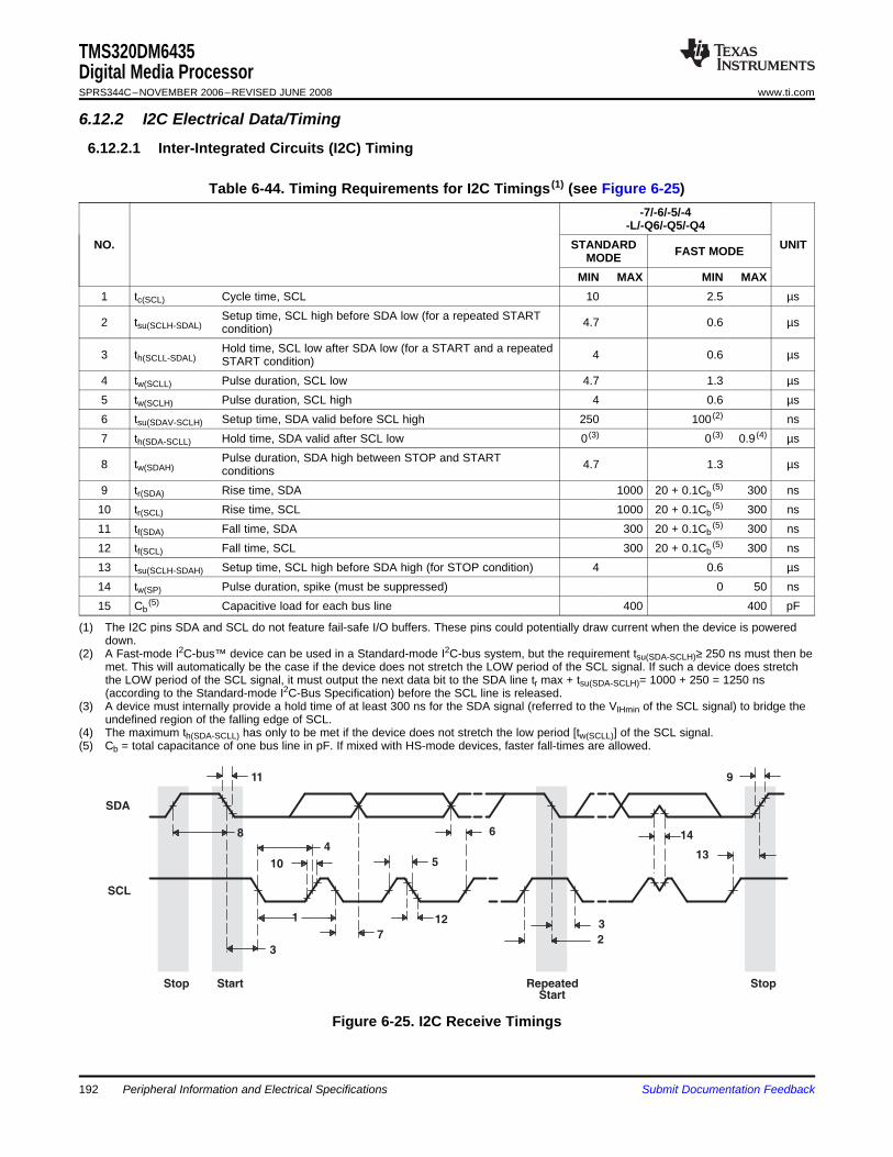
6.12.2 I2C Electrical Data/Timing
6.12.2.1 Inter-Integrated Circuits (I2C) Timing
10
8
4
3
7
12
5
6 14
2
3
13
Stop Start Repeated
Start
Stop
SDA
SCL
1
11 9
TMS320DM6435Digital Media ProcessorSPRS344C–NOVEMBER 2006–REVISED JUNE 2008 www.ti.com
Table 6-44. Timing Requirements for I2C Timings (1) (see Figure 6-25)-7/-6/-5/-4
-L/-Q6/-Q5/-Q4NO. STANDARD UNITFAST MODEMODE
MIN MAX MIN MAX1 tc(SCL) Cycle time, SCL 10 2.5 µs
Setup time, SCL high before SDA low (for a repeated START2 tsu(SCLH-SDAL) 4.7 0.6 µscondition)Hold time, SCL low after SDA low (for a START and a repeated3 th(SCLL-SDAL) 4 0.6 µsSTART condition)
4 tw(SCLL) Pulse duration, SCL low 4.7 1.3 µs5 tw(SCLH) Pulse duration, SCL high 4 0.6 µs6 tsu(SDAV-SCLH) Setup time, SDA valid before SCL high 250 100 (2) ns7 th(SDA-SCLL) Hold time, SDA valid after SCL low 0 (3) 0 (3) 0.9 (4) µs
Pulse duration, SDA high between STOP and START8 tw(SDAH) 4.7 1.3 µsconditions9 tr(SDA) Rise time, SDA 1000 20 + 0.1Cb
(5) 300 ns10 tr(SCL) Rise time, SCL 1000 20 + 0.1Cb
(5) 300 ns11 tf(SDA) Fall time, SDA 300 20 + 0.1Cb
(5) 300 ns12 tf(SCL) Fall time, SCL 300 20 + 0.1Cb
(5) 300 ns13 tsu(SCLH-SDAH) Setup time, SCL high before SDA high (for STOP condition) 4 0.6 µs14 tw(SP) Pulse duration, spike (must be suppressed) 0 50 ns15 Cb
(5) Capacitive load for each bus line 400 400 pF
(1) The I2C pins SDA and SCL do not feature fail-safe I/O buffers. These pins could potentially draw current when the device is powereddown.
(2) A Fast-mode I2C-bus™ device can be used in a Standard-mode I2C-bus system, but the requirement tsu(SDA-SCLH)≥ 250 ns must then bemet. This will automatically be the case if the device does not stretch the LOW period of the SCL signal. If such a device does stretchthe LOW period of the SCL signal, it must output the next data bit to the SDA line tr max + tsu(SDA-SCLH)= 1000 + 250 = 1250 ns(according to the Standard-mode I2C-Bus Specification) before the SCL line is released.
(3) A device must internally provide a hold time of at least 300 ns for the SDA signal (referred to the VIHmin of the SCL signal) to bridge theundefined region of the falling edge of SCL.
(4) The maximum th(SDA-SCLL) has only to be met if the device does not stretch the low period [tw(SCLL)] of the SCL signal.(5) Cb = total capacitance of one bus line in pF. If mixed with HS-mode devices, faster fall-times are allowed.
Figure 6-25. I2C Receive Timings
Peripheral Information and Electrical Specifications192 Submit Documentation Feedback
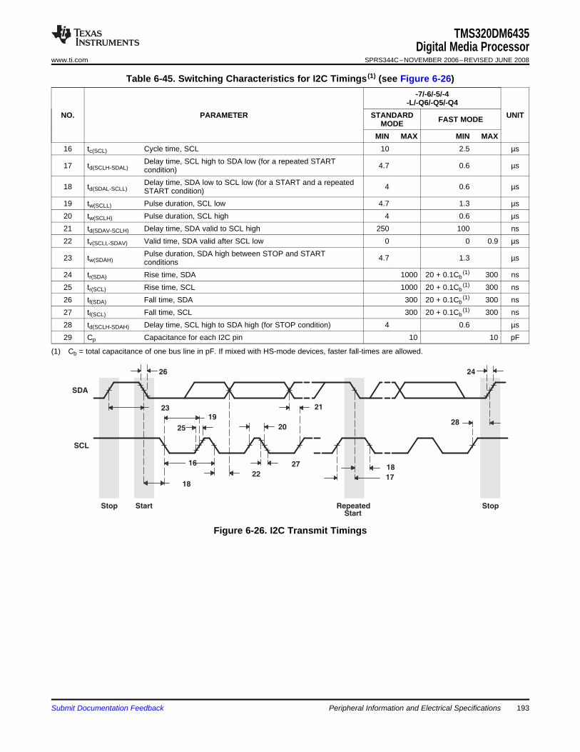
25
23
19
18
22
27
20
21
17
18
28
Stop Start Repeated
Start
Stop
SDA
SCL
16
26 24
TMS320DM6435Digital Media Processor
www.ti.com SPRS344C–NOVEMBER 2006–REVISED JUNE 2008
Table 6-45. Switching Characteristics for I2C Timings (1) (see Figure 6-26)-7/-6/-5/-4
-L/-Q6/-Q5/-Q4NO. PARAMETER STANDARD UNITFAST MODEMODE
MIN MAX MIN MAX16 tc(SCL) Cycle time, SCL 10 2.5 µs
Delay time, SCL high to SDA low (for a repeated START17 td(SCLH-SDAL) 4.7 0.6 µscondition)Delay time, SDA low to SCL low (for a START and a repeated18 td(SDAL-SCLL) 4 0.6 µsSTART condition)
19 tw(SCLL) Pulse duration, SCL low 4.7 1.3 µs20 tw(SCLH) Pulse duration, SCL high 4 0.6 µs21 td(SDAV-SCLH) Delay time, SDA valid to SCL high 250 100 ns22 tv(SCLL-SDAV) Valid time, SDA valid after SCL low 0 0 0.9 µs
Pulse duration, SDA high between STOP and START23 tw(SDAH) 4.7 1.3 µsconditions24 tr(SDA) Rise time, SDA 1000 20 + 0.1Cb
(1) 300 ns25 tr(SCL) Rise time, SCL 1000 20 + 0.1Cb
(1) 300 ns26 tf(SDA) Fall time, SDA 300 20 + 0.1Cb
(1) 300 ns27 tf(SCL) Fall time, SCL 300 20 + 0.1Cb
(1) 300 ns28 td(SCLH-SDAH) Delay time, SCL high to SDA high (for STOP condition) 4 0.6 µs29 Cp Capacitance for each I2C pin 10 10 pF
(1) Cb = total capacitance of one bus line in pF. If mixed with HS-mode devices, faster fall-times are allowed.
Figure 6-26. I2C Transmit Timings
Submit Documentation Feedback Peripheral Information and Electrical Specifications 193
6.13 Host-Port Interface (HPI) Peripheral
6.13.1 HPI Device-Specific Information
6.13.2 HPI Peripheral Register Description(s)
TMS320DM6435Digital Media ProcessorSPRS344C–NOVEMBER 2006–REVISED JUNE 2008 www.ti.com
The DM6435 device includes a user-configurable 16-bit Host-port interface (HPI16).
Software handshaking via the HRDY bit of the Host Port Control Register (HPIC) is not supported on theDM6435.
The DM6435 HPI does not support the HAS feature. For proper device operation, the HAS pin must bepulled up via an external resistor.
Table 6-46. HPI Control RegistersHEX ADDRESS RANGE ACRONYM REGISTER NAME COMMENTS
01C6 7800 PID Peripheral Identification RegisterThe CPU has read/write
01C6 7804 PWREMU_MGMT HPI power and emulation management register access to thePWREMU_MGMT register.
01C6 7808 - 01C6 7824 - Reserved01C6 7828 - Reserved01C6 782C - Reserved
The Host and the CPU both01C6 7830 HPIC HPI control register have read/write access to the
HPIC register.HPIA HPI address register The Host has read/write01C6 7834 (HPIAW) (1) (Write) access to the HPIA registers.
The CPU has only readHPIA HPI address register01C6 7838 access to the HPIA registers.(HPIAR) (1) (Read)01C6 780C - 01C6 7FFF - Reserved
(1) There are two 32-bit HPIA registers: HPIAR for read operations and HPIAW for write operations. The HPI can be configured such thatHPIAR and HPIAW act as a single 32-bit HPIA (single-HPIA mode) or as two separate 32-bit HPIAs (dual-HPIA mode) from theperspective of the Host. The CPU can access HPIAW and HPIAR independently. For more details about the HPIA registers and theirmodes, see the TMS320C643x DMP Host Port Interface (HPI) User's Guide (literature number SPRU998).
Peripheral Information and Electrical Specifications194 Submit Documentation Feedback
6.13.3 HPI Electrical Data/Timing
TMS320DM6435Digital Media Processor
www.ti.com SPRS344C–NOVEMBER 2006–REVISED JUNE 2008
Table 6-47. Timing Requirements for Host-Port Interface Cycles (1) (2) (see Figure 6-27 and Figure 6-28)-7/-6/-5/-4
-L/-Q6/-Q5/-Q4NO. UNITMIN MAX
1 tsu(SELV-HSTBL) Setup time, select signals (3) valid before HSTROBE low 5 ns2 th(HSTBL-SELV) Hold time, select signals (3) valid after HSTROBE low 2 ns3 tw(HSTBL) Pulse duration, HSTROBE active low 15 ns4 tw(HSTBH) Pulse duration, HSTROBE inactive high between consecutive accesses 2M ns11 tsu(HDV-HSTBH) Setup time, host data valid before HSTROBE high 5 ns12 th(HSTBH-HDV) Hold time, host data valid after HSTROBE high 0 ns
Hold time, HSTROBE high after HRDY low. HSTROBE should not be13 th(HRDYL-HSTBL) inactivated until HRDY is active (low); otherwise, HPI writes will not 0 ns
complete properly.
(1) HSTROBE refers to the following logical operation on HCS, HDS1, and HDS2: [NOT(HDS1 XOR HDS2)] OR HCS.(2) M = SYSCLK3 period = (CPU clock frequency)/6 in ns. For example, when running parts at 600 MHz, use 10 ns.(3) Select signals include: HCNTL[1:0], HR/W and HHWIL.
Submit Documentation Feedback Peripheral Information and Electrical Specifications 195
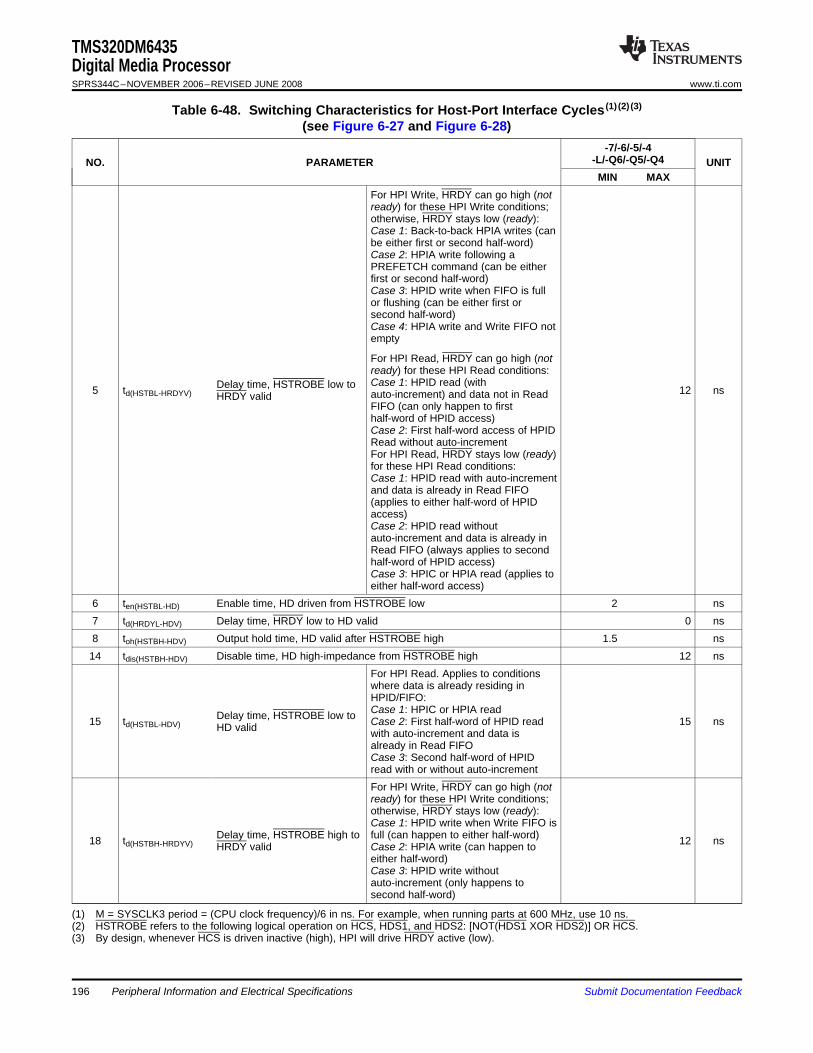
TMS320DM6435Digital Media ProcessorSPRS344C–NOVEMBER 2006–REVISED JUNE 2008 www.ti.com
Table 6-48. Switching Characteristics for Host-Port Interface Cycles (1) (2) (3)
(see Figure 6-27 and Figure 6-28)-7/-6/-5/-4
-L/-Q6/-Q5/-Q4NO. PARAMETER UNITMIN MAX
For HPI Write, HRDY can go high (notready) for these HPI Write conditions;otherwise, HRDY stays low (ready):Case 1: Back-to-back HPIA writes (canbe either first or second half-word)Case 2: HPIA write following aPREFETCH command (can be eitherfirst or second half-word)Case 3: HPID write when FIFO is fullor flushing (can be either first orsecond half-word)Case 4: HPIA write and Write FIFO notempty
For HPI Read, HRDY can go high (notready) for these HPI Read conditions:Case 1: HPID read (withDelay time, HSTROBE low to5 td(HSTBL-HRDYV) 12 nsauto-increment) and data not in ReadHRDY validFIFO (can only happen to firsthalf-word of HPID access)Case 2: First half-word access of HPIDRead without auto-incrementFor HPI Read, HRDY stays low (ready)for these HPI Read conditions:Case 1: HPID read with auto-incrementand data is already in Read FIFO(applies to either half-word of HPIDaccess)Case 2: HPID read withoutauto-increment and data is already inRead FIFO (always applies to secondhalf-word of HPID access)Case 3: HPIC or HPIA read (applies toeither half-word access)
6 ten(HSTBL-HD) Enable time, HD driven from HSTROBE low 2 ns7 td(HRDYL-HDV) Delay time, HRDY low to HD valid 0 ns8 toh(HSTBH-HDV) Output hold time, HD valid after HSTROBE high 1.5 ns
14 tdis(HSTBH-HDV) Disable time, HD high-impedance from HSTROBE high 12 nsFor HPI Read. Applies to conditionswhere data is already residing inHPID/FIFO:Case 1: HPIC or HPIA readDelay time, HSTROBE low to15 td(HSTBL-HDV) Case 2: First half-word of HPID read 15 nsHD valid with auto-increment and data isalready in Read FIFOCase 3: Second half-word of HPIDread with or without auto-incrementFor HPI Write, HRDY can go high (notready) for these HPI Write conditions;otherwise, HRDY stays low (ready):Case 1: HPID write when Write FIFO is
Delay time, HSTROBE high to full (can happen to either half-word)18 td(HSTBH-HRDYV) 12 nsHRDY valid Case 2: HPIA write (can happen toeither half-word)Case 3: HPID write withoutauto-increment (only happens tosecond half-word)
(1) M = SYSCLK3 period = (CPU clock frequency)/6 in ns. For example, when running parts at 600 MHz, use 10 ns.(2) HSTROBE refers to the following logical operation on HCS, HDS1, and HDS2: [NOT(HDS1 XOR HDS2)] OR HCS.(3) By design, whenever HCS is driven inactive (high), HPI will drive HRDY active (low).
Peripheral Information and Electrical Specifications196 Submit Documentation Feedback
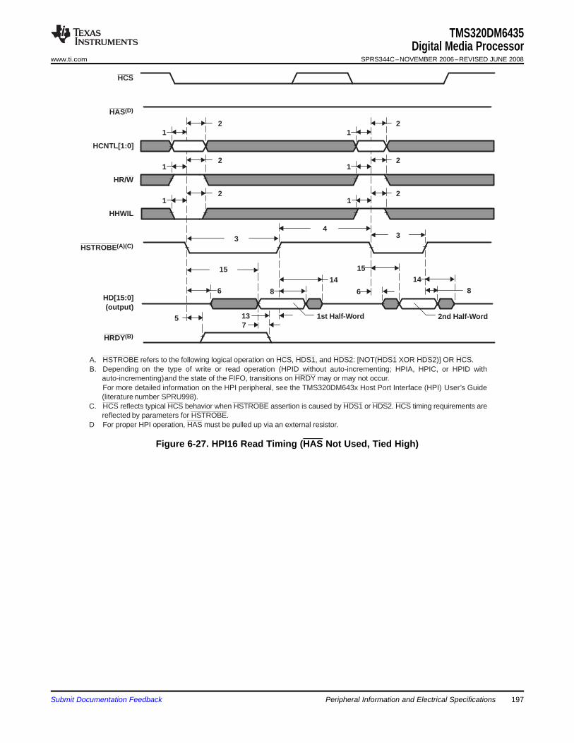
HCS
HAS(D)
HCNTL[1:0]
HR/W
HHWIL
HSTROBE(A)(C)
HD[15:0](output)
HRDY(B)
12
12
12
5
6
34
3
12
12
12
8
14
15
14
8
71st Half-W ord 2nd Half-W ord
6
13
15
A. HSTROBE refers to the following logical operation on HCS, HDS1, and HDS2: [NOT(HDS1 XOR HDS2)] OR HCS.B. Depending on the type of write or read operation (HPID without auto-incrementing; HPIA, HPIC, or HPID with
auto-incrementing) and the state of the FIFO, transitions on HRDY may or may not occur.For more detailed information on the HPI peripheral, see the TMS320DM643x Host Port Interface (HPI) User’s Guide(literature number SPRU998).
C. HCS reflects typical HCS behavior when HSTROBE assertion is caused by HDS1 or HDS2. HCS timing requirements arereflected by parameters for HSTROBE.
D For proper HPI operation, HAS must be pulled up via an external resistor.
TMS320DM6435Digital Media Processor
www.ti.com SPRS344C–NOVEMBER 2006–REVISED JUNE 2008
Figure 6-27. HPI16 Read Timing (HAS Not Used, Tied High)
Submit Documentation Feedback Peripheral Information and Electrical Specifications 197
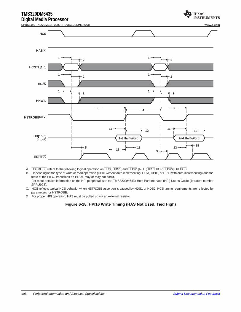
HAS(D)
HCNTL[1:0]
HR/W
HHWIL
HSTROBE(A)(C)
HCS
HD[15:0](input)
HRDY(B)
21
21
12
21
21
12
34
3
1112
1813
5185
1112
13
2nd Half-W ord1st Half-W ord
A. HSTROBE refers to the following logical operation on HCS, HDS1, and HDS2: [NOT(HDS1 XOR HDS2)] OR HCS.B. Depending on the type of write or read operation (HPID without auto-incrementing; HPIA, HPIC, or HPID with auto-incrementing) and the
state of the FIFO, transitions on HRDY may or may not occur.For more detailed information on the HPI peripheral, see the TMS320DM643x Host Port Interface (HPI) User’s Guide (literature numberSPRU998).
C. HCS reflects typical HCS behavior when HSTROBE assertion is caused by HDS1 or HDS2. HCS timing requirements are reflected byparameters for HSTROBE.
D For proper HPI operation, HAS must be pulled up via an external resistor.
TMS320DM6435Digital Media ProcessorSPRS344C–NOVEMBER 2006–REVISED JUNE 2008 www.ti.com
Figure 6-28. HPI16 Write Timing (HAS Not Used, Tied High)
198 Peripheral Information and Electrical Specifications Submit Documentation Feedback
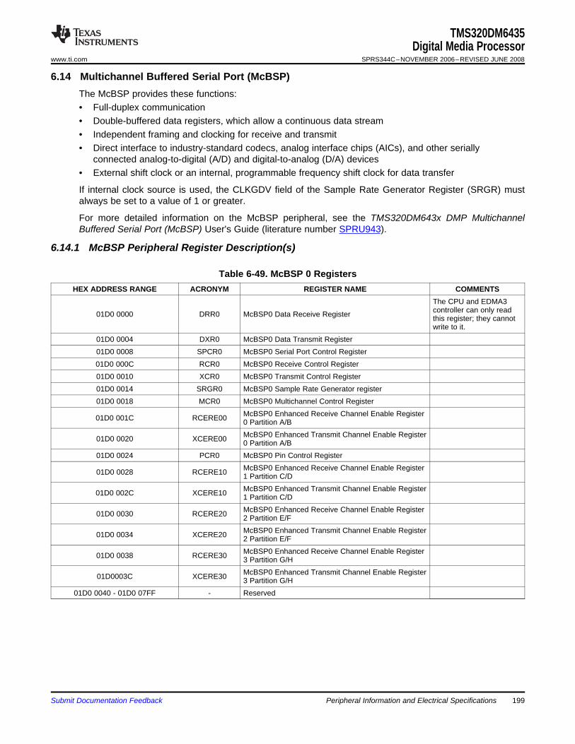
6.14 Multichannel Buffered Serial Port (McBSP)
6.14.1 McBSP Peripheral Register Description(s)
TMS320DM6435Digital Media Processor
www.ti.com SPRS344C–NOVEMBER 2006–REVISED JUNE 2008
The McBSP provides these functions:• Full-duplex communication• Double-buffered data registers, which allow a continuous data stream• Independent framing and clocking for receive and transmit• Direct interface to industry-standard codecs, analog interface chips (AICs), and other serially
connected analog-to-digital (A/D) and digital-to-analog (D/A) devices• External shift clock or an internal, programmable frequency shift clock for data transfer
If internal clock source is used, the CLKGDV field of the Sample Rate Generator Register (SRGR) mustalways be set to a value of 1 or greater.
For more detailed information on the McBSP peripheral, see the TMS320DM643x DMP MultichannelBuffered Serial Port (McBSP) User's Guide (literature number SPRU943).
Table 6-49. McBSP 0 RegistersHEX ADDRESS RANGE ACRONYM REGISTER NAME COMMENTS
The CPU and EDMA3controller can only read01D0 0000 DRR0 McBSP0 Data Receive Register this register; they cannotwrite to it.
01D0 0004 DXR0 McBSP0 Data Transmit Register01D0 0008 SPCR0 McBSP0 Serial Port Control Register01D0 000C RCR0 McBSP0 Receive Control Register01D0 0010 XCR0 McBSP0 Transmit Control Register01D0 0014 SRGR0 McBSP0 Sample Rate Generator register01D0 0018 MCR0 McBSP0 Multichannel Control Register
McBSP0 Enhanced Receive Channel Enable Register01D0 001C RCERE00 0 Partition A/BMcBSP0 Enhanced Transmit Channel Enable Register01D0 0020 XCERE00 0 Partition A/B
01D0 0024 PCR0 McBSP0 Pin Control RegisterMcBSP0 Enhanced Receive Channel Enable Register01D0 0028 RCERE10 1 Partition C/DMcBSP0 Enhanced Transmit Channel Enable Register01D0 002C XCERE10 1 Partition C/DMcBSP0 Enhanced Receive Channel Enable Register01D0 0030 RCERE20 2 Partition E/FMcBSP0 Enhanced Transmit Channel Enable Register01D0 0034 XCERE20 2 Partition E/FMcBSP0 Enhanced Receive Channel Enable Register01D0 0038 RCERE30 3 Partition G/HMcBSP0 Enhanced Transmit Channel Enable Register01D0003C XCERE30 3 Partition G/H
01D0 0040 - 01D0 07FF - Reserved
Submit Documentation Feedback Peripheral Information and Electrical Specifications 199
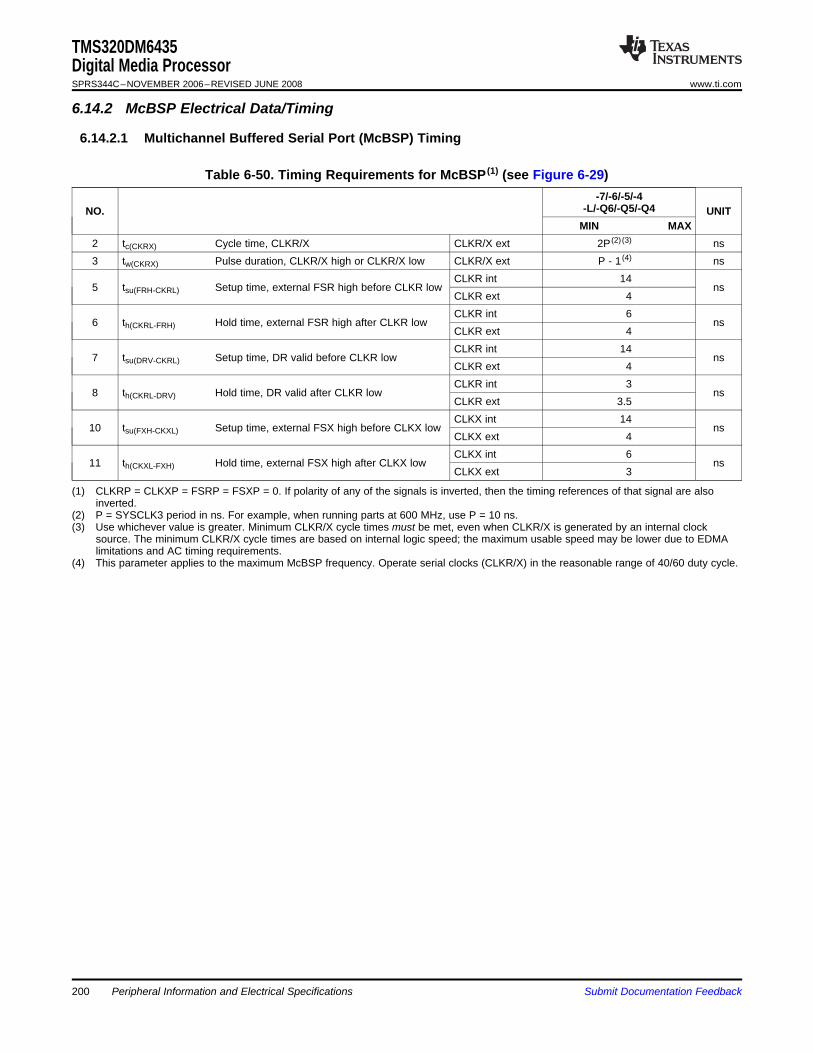
6.14.2 McBSP Electrical Data/Timing
6.14.2.1 Multichannel Buffered Serial Port (McBSP) Timing
TMS320DM6435Digital Media ProcessorSPRS344C–NOVEMBER 2006–REVISED JUNE 2008 www.ti.com
Table 6-50. Timing Requirements for McBSP (1) (see Figure 6-29)-7/-6/-5/-4
-L/-Q6/-Q5/-Q4NO. UNITMIN MAX
2 tc(CKRX) Cycle time, CLKR/X CLKR/X ext 2P (2) (3) ns3 tw(CKRX) Pulse duration, CLKR/X high or CLKR/X low CLKR/X ext P - 1 (4) ns
CLKR int 145 tsu(FRH-CKRL) Setup time, external FSR high before CLKR low ns
CLKR ext 4CLKR int 6
6 th(CKRL-FRH) Hold time, external FSR high after CLKR low nsCLKR ext 4CLKR int 14
7 tsu(DRV-CKRL) Setup time, DR valid before CLKR low nsCLKR ext 4CLKR int 3
8 th(CKRL-DRV) Hold time, DR valid after CLKR low nsCLKR ext 3.5CLKX int 14
10 tsu(FXH-CKXL) Setup time, external FSX high before CLKX low nsCLKX ext 4CLKX int 6
11 th(CKXL-FXH) Hold time, external FSX high after CLKX low nsCLKX ext 3
(1) CLKRP = CLKXP = FSRP = FSXP = 0. If polarity of any of the signals is inverted, then the timing references of that signal are alsoinverted.
(2) P = SYSCLK3 period in ns. For example, when running parts at 600 MHz, use P = 10 ns.(3) Use whichever value is greater. Minimum CLKR/X cycle times must be met, even when CLKR/X is generated by an internal clock
source. The minimum CLKR/X cycle times are based on internal logic speed; the maximum usable speed may be lower due to EDMAlimitations and AC timing requirements.
(4) This parameter applies to the maximum McBSP frequency. Operate serial clocks (CLKR/X) in the reasonable range of 40/60 duty cycle.
Peripheral Information and Electrical Specifications200 Submit Documentation Feedback

TMS320DM6435Digital Media Processor
www.ti.com SPRS344C–NOVEMBER 2006–REVISED JUNE 2008
Table 6-51. Switching Characteristics Over Recommended Operating Conditions for McBSP (1) (2)
(see Figure 6-29)-7/-6/-5/-4
-L/-Q6/-Q5/-Q4NO. PARAMETER UNITMIN MAX
Delay time, CLKS high to CLKR/X high for internal CLKR/X1 td(CKSH-CKRXH) 3 10 nsgenerated from CLKS input2 tc(CKRX) Cycle time, CLKR/X CLKR/X int 2P (3) (4) (5) ns3 tw(CKRX) Pulse duration, CLKR/X high or CLKR/X low CLKR/X int C - 2 (6) C + 2 (6) ns4 td(CKRH-FRV) Delay time, CLKR high to internal FSR valid CLKR int -4 5.5 ns
CLKX int -4 5.59 td(CKXH-FXV) Delay time, CLKX high to internal FSX valid ns
CLKX ext 2.5 14.5CLKX int -5.5 7.5Disable time, DX high impedance following12 tdis(CKXH-DXHZ) nslast data bit from CLKX high CLKX ext -2.1 16CLKX int -4 + D1 (7) 5.5 + D2 (7)
13 td(CKXH-DXV) Delay time, CLKX high to DX valid nsCLKX ext 2.5 + D1 (7) 14.5 + D2 (7)
Delay time, FSX high to DX valid FSX int -4 (8) 5 (8)
14 td(FXH-DXV) nsONLY applies when in data FSX ext 1 (8) 14.5 (8)delay 0 (XDATDLY = 00b) mode
(1) CLKRP = CLKXP = FSRP = FSXP = 0. If polarity of any of the signals is inverted, then the timing references of that signal are alsoinverted.
(2) Minimum delay times also represent minimum output hold times.(3) Minimum CLKR/X cycle times must be met, even when CLKR/X is generated by an internal clock source. Minimum CLKR/X cycle times
are based on internal logic speed; the maximum usable speed may be lower due to EDMA limitations and AC timing requirements.(4) P = SYSCLK3 period in ns. For example, when running parts at 600 MHz, use P = 10 ns.(5) Use whichever value is greater.(6) C = H or L
S = sample rate generator input clock = P if CLKSM = 1 (P = SYSCLK3 period)S = sample rate generator input clock = P_clks if CLKSM = 0 (P_clks = CLKS period)H = CLKX high pulse width = (CLKGDV/2 + 1) * S if CLKGDV is evenH = (CLKGDV + 1)/2 * S if CLKGDV is oddL = CLKX low pulse width = (CLKGDV/2) * S if CLKGDV is evenL = (CLKGDV + 1)/2 * S if CLKGDV is oddCLKGDV should be set appropriately to ensure the McBSP bit rate does not exceed the maximum limit (see (4) above).
(7) Extra delay from CLKX high to DX valid applies only to the first data bit of a device, if and only if DXENA = 1 in SPCR.if DXENA = 0, then D1 = D2 = 0if DXENA = 1, then D1 = 6P, D2 = 12P
(8) Extra delay from FSX high to DX valid applies only to the first data bit of a device, if and only if DXENA = 1 in SPCR.if DXENA = 0, then D1 = D2 = 0if DXENA = 1, then D1 = 6P, D2 = 12P
Submit Documentation Feedback Peripheral Information and Electrical Specifications 201
Bit(n-1) (n-2) (n-3)
Bit 0 Bit(n-1) (n-2) (n-3)
1412
1110
9
33
2
87
65
44
3
1
32
CLKS
CLKR
FSR (int)
FSR (ext)
DR
CLKX
FSX (int)
FSX (ext)
FSX (XDATDLY=00b)
DX
13 (A)
13 (A)
21
CLKS
FSR external
CLKR/X (no need to resync)
CLKR/X (needs resync)
TMS320DM6435Digital Media ProcessorSPRS344C–NOVEMBER 2006–REVISED JUNE 2008 www.ti.com
A. Parameter No. 13 applies to the first data bit only when XDATDLY ≠ 0.
Figure 6-29. McBSP Timing(B)
Table 6-52. Timing Requirements for FSR When GSYNC = 1 (see Figure 6-30)-7/-6/-5/-4
-L/-Q6/-Q5/-Q4NO. UNITMIN MAX
1 tsu(FRH-CKSH) Setup time, FSR high before CLKS high 4 ns2 th(CKSH-FRH) Hold time, FSR high after CLKS high 4 ns
Figure 6-30. FSR Timing When GSYNC = 1
Peripheral Information and Electrical Specifications202 Submit Documentation Feedback
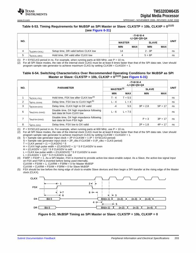
Bit 0 Bit(n-1) (n-2) (n-3) (n-4)
Bit 0 Bit(n-1) (n-2) (n-3) (n-4)5
4
387
6
21
CLKX
FSX
DX
DR
TMS320DM6435Digital Media Processor
www.ti.com SPRS344C–NOVEMBER 2006–REVISED JUNE 2008
Table 6-53. Timing Requirements for McBSP as SPI Master or Slave: CLKSTP = 10b, CLKXP = 0 (1) (2)
(see Figure 6-31)-7/-6/-5/-4
-L/-Q6/-Q5/-Q4NO. UNITMASTER SLAVE
MIN MAX MIN MAX4 tsu(DRV-CKXL) Setup time, DR valid before CLKX low 14 2 - 3P ns5 th(CKXL-DRV) Hold time, DR valid after CLKX low 4 5 + 6P ns
(1) P = SYSCLK3 period in ns. For example, when running parts at 600 MHz, use P = 10 ns.(2) For all SPI Slave modes, the rate of the internal clock CLKG must be at least 8 times faster than that of the SPI data rate. User should
program sample rate generator to achieve maximum CLKG by setting CLKSM = CLKGDV = 1.
Table 6-54. Switching Characteristics Over Recommended Operating Conditions for McBSP as SPIMaster or Slave: CLKSTP = 10b, CLKXP = 0 (1) (2) (see Figure 6-31)
-7/-6/-5/-4-L/-Q6/-Q5/-Q4
NO. PARAMETER UNITMASTER (3) SLAVEMIN MAX MIN MAX
1 th(CKXL-FXL) Hold time, FSX low after CLKX low (4) T - 4 T + 5.5 ns2 td(FXL-CKXH) Delay time, FSX low to CLKX high (5) L - 4 L + 4 ns3 td(CKXH-DXV) Delay time, CLKX high to DX valid -4 5.5 3P + 2.8 5P + 17 ns
Disable time, DX high impedance following6 tdis(CKXL-DXHZ) L - 6 L + 7.5 nslast data bit from CLKX lowDisable time, DX high impedance following7 tdis(FXH-DXHZ) P + 3 3P + 17 nslast data bit from FSX high
8 td(FXL-DXV) Delay time, FSX low to DX valid 2P + 1.8 4P + 17 ns
(1) P = SYSCLK3 period in ns. For example, when running parts at 600 MHz, use P = 10 ns.(2) For all SPI Slave modes, the rate of the internal clock CLKG must be at least 8 times faster than that of the SPI data rate. User should
program sample rate generator to achieve maximum CLKG by setting CLKSM = CLKGDV = 1.(3) S = Sample rate generator input clock = 2P if CLKSM = 1 (P = SYSCLK3 period)
S = Sample rate generator input clock = 2P_clks if CLKSM = 0 (P_clks = CLKS period)T = CLKX period = (1 + CLKGDV) * SH = CLKX high pulse width = (CLKGDV/2 + 1) * S if CLKGDV is evenH = (CLKGDV + 1)/2 * S if CLKGDV is oddL = CLKX low pulse width = (CLKGDV/2) * S if CLKGDV is evenL = (CLKGDV + 1)/2 * S if CLKGDV is odd
(4) FSRP = FSXP = 1. As a SPI Master, FSX is inverted to provide active-low slave-enable output. As a Slave, the active-low signal inputon FSX and FSR is inverted before being used internally.CLKXM = FSXM = 1, CLKRM = FSRM = 0 for Master McBSPCLKXM = CLKRM = FSXM = FSRM = 0 for Slave McBSP
(5) FSX should be low before the rising edge of clock to enable Slave devices and then begin a SPI transfer at the rising edge of the Masterclock (CLKX).
Figure 6-31. McBSP Timing as SPI Master or Slave: CLKSTP = 10b, CLKXP = 0
Submit Documentation Feedback Peripheral Information and Electrical Specifications 203
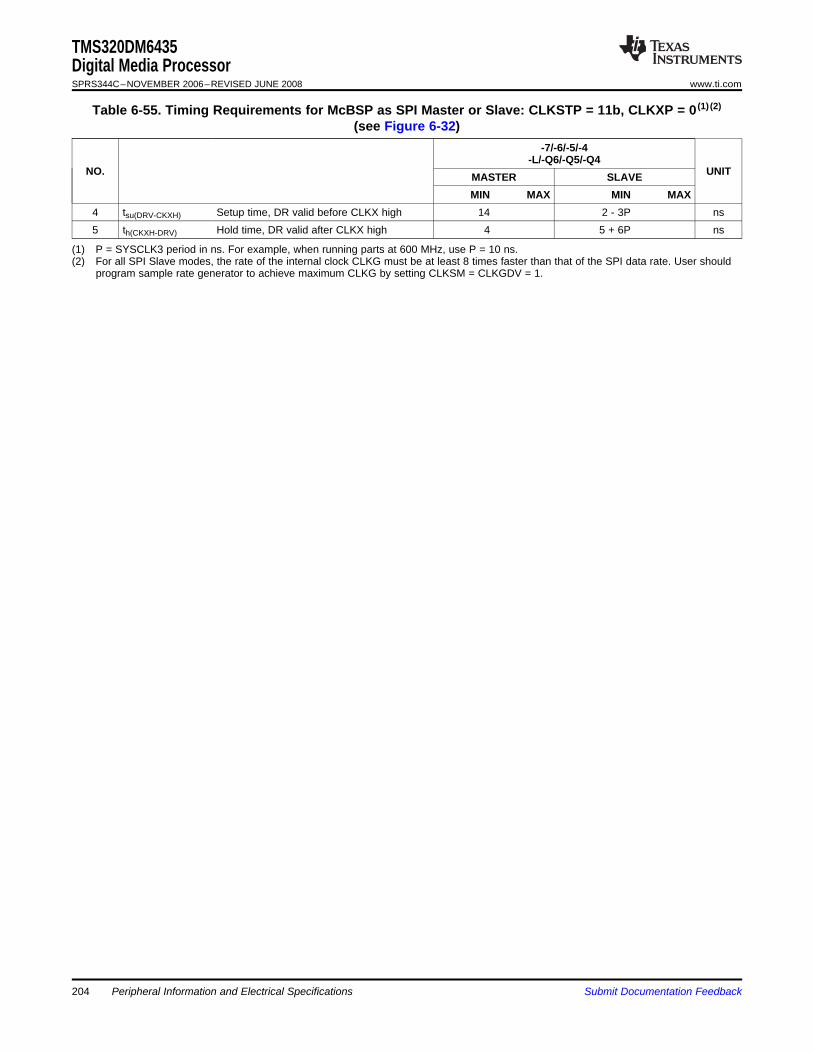
TMS320DM6435Digital Media ProcessorSPRS344C–NOVEMBER 2006–REVISED JUNE 2008 www.ti.com
Table 6-55. Timing Requirements for McBSP as SPI Master or Slave: CLKSTP = 11b, CLKXP = 0 (1) (2)
(see Figure 6-32)-7/-6/-5/-4
-L/-Q6/-Q5/-Q4NO. UNITMASTER SLAVE
MIN MAX MIN MAX4 tsu(DRV-CKXH) Setup time, DR valid before CLKX high 14 2 - 3P ns5 th(CKXH-DRV) Hold time, DR valid after CLKX high 4 5 + 6P ns
(1) P = SYSCLK3 period in ns. For example, when running parts at 600 MHz, use P = 10 ns.(2) For all SPI Slave modes, the rate of the internal clock CLKG must be at least 8 times faster than that of the SPI data rate. User should
program sample rate generator to achieve maximum CLKG by setting CLKSM = CLKGDV = 1.
Peripheral Information and Electrical Specifications204 Submit Documentation Feedback
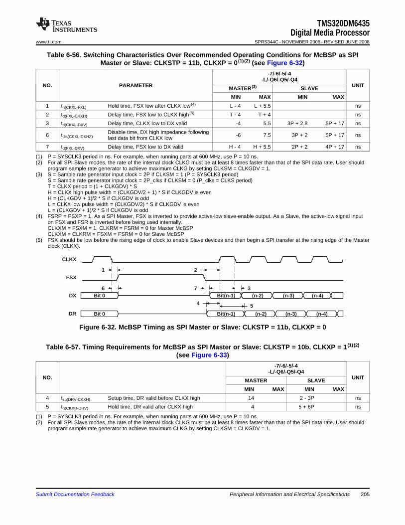
Bit 0 Bit(n-1) (n-2) (n-3) (n-4)
Bit 0 Bit(n-1) (n-2) (n-3) (n-4)
4
376
21
CLKX
FSX
DX
DR
5
TMS320DM6435Digital Media Processor
www.ti.com SPRS344C–NOVEMBER 2006–REVISED JUNE 2008
Table 6-56. Switching Characteristics Over Recommended Operating Conditions for McBSP as SPIMaster or Slave: CLKSTP = 11b, CLKXP = 0 (1) (2) (see Figure 6-32)
-7/-6/-5/-4-L/-Q6/-Q5/-Q4
NO. PARAMETER UNITMASTER (3) SLAVEMIN MAX MIN MAX
1 th(CKXL-FXL) Hold time, FSX low after CLKX low (4) L - 4 L + 5.5 ns2 td(FXL-CKXH) Delay time, FSX low to CLKX high (5) T - 4 T + 4 ns3 td(CKXL-DXV) Delay time, CLKX low to DX valid -4 5.5 3P + 2.8 5P + 17 ns
Disable time, DX high impedance following6 tdis(CKXL-DXHZ) -6 7.5 3P + 2 5P + 17 nslast data bit from CLKX low7 td(FXL-DXV) Delay time, FSX low to DX valid H - 4 H + 5.5 2P + 2 4P + 17 ns
(1) P = SYSCLK3 period in ns. For example, when running parts at 600 MHz, use P = 10 ns.(2) For all SPI Slave modes, the rate of the internal clock CLKG must be at least 8 times faster than that of the SPI data rate. User should
program sample rate generator to achieve maximum CLKG by setting CLKSM = CLKGDV = 1.(3) S = Sample rate generator input clock = 2P if CLKSM = 1 (P = SYSCLK3 period)
S = Sample rate generator input clock = 2P_clks if CLKSM = 0 (P_clks = CLKS period)T = CLKX period = (1 + CLKGDV) * SH = CLKX high pulse width = (CLKGDV/2 + 1) * S if CLKGDV is evenH = (CLKGDV + 1)/2 * S if CLKGDV is oddL = CLKX low pulse width = (CLKGDV/2) * S if CLKGDV is evenL = (CLKGDV + 1)/2 * S if CLKGDV is odd
(4) FSRP = FSXP = 1. As a SPI Master, FSX is inverted to provide active-low slave-enable output. As a Slave, the active-low signal inputon FSX and FSR is inverted before being used internally.CLKXM = FSXM = 1, CLKRM = FSRM = 0 for Master McBSPCLKXM = CLKRM = FSXM = FSRM = 0 for Slave McBSP
(5) FSX should be low before the rising edge of clock to enable Slave devices and then begin a SPI transfer at the rising edge of the Masterclock (CLKX).
Figure 6-32. McBSP Timing as SPI Master or Slave: CLKSTP = 11b, CLKXP = 0
Table 6-57. Timing Requirements for McBSP as SPI Master or Slave: CLKSTP = 10b, CLKXP = 1 (1) (2)
(see Figure 6-33)-7/-6/-5/-4
-L/-Q6/-Q5/-Q4NO. UNITMASTER SLAVE
MIN MAX MIN MAX4 tsu(DRV-CKXH) Setup time, DR valid before CLKX high 14 2 - 3P ns5 th(CKXH-DRV) Hold time, DR valid after CLKX high 4 5 + 6P ns
(1) P = SYSCLK3 period in ns. For example, when running parts at 600 MHz, use P = 10 ns.(2) For all SPI Slave modes, the rate of the internal clock CLKG must be at least 8 times faster than that of the SPI data rate. User should
program sample rate generator to achieve maximum CLKG by setting CLKSM = CLKGDV = 1.
Submit Documentation Feedback Peripheral Information and Electrical Specifications 205
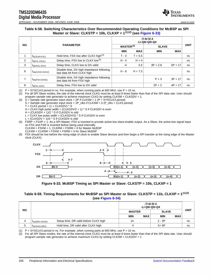
Bit 0 Bit(n-1) (n-2) (n-3) (n-4)
Bit 0 Bit(n-1) (n-2) (n-3) (n-4)54
387
6
21
CLKX
FSX
DX
DR
TMS320DM6435Digital Media ProcessorSPRS344C–NOVEMBER 2006–REVISED JUNE 2008 www.ti.com
Table 6-58. Switching Characteristics Over Recommended Operating Conditions for McBSP as SPIMaster or Slave: CLKSTP = 10b, CLKXP = 1 (1) (2) (see Figure 6-33)
-7/-6/-5/-4-L/-Q6/-Q5/-Q4
NO. PARAMETER UNITMASTER (3) SLAVEMIN MAX MIN MAX
1 th(CKXH-FXL) Hold time, FSX low after CLKX high (4) T - 4 T + 5.5 ns2 td(FXL-CKXL) Delay time, FSX low to CLKX low (5) H - 4 H + 4 ns3 td(CKXL-DXV) Delay time, CLKX low to DX valid -4 5.5 3P + 2.8 5P + 17 ns
Disable time, DX high impedance following6 tdis(CKXH-DXHZ) H - 6 H + 7.5 nslast data bit from CLKX highDisable time, DX high impedance following7 tdis(FXH-DXHZ) P + 3 3P + 17 nslast data bit from FSX high
8 td(FXL-DXV) Delay time, FSX low to DX valid 2P + 2 4P + 17 ns
(1) P = SYSCLK3 period in ns. For example, when running parts at 600 MHz, use P = 10 ns.(2) For all SPI Slave modes, the rate of the internal clock CLKG must be at least 8 times faster than that of the SPI data rate. User should
program sample rate generator to achieve maximum CLKG by setting CLKSM = CLKGDV = 1.(3) S = Sample rate generator input clock = 2P if CLKSM = 1 (P = SYSCLK3 period)
S = Sample rate generator input clock = 2P_clks if CLKSM = 0 (P_clks = CLKS period)T = CLKX period = (1 + CLKGDV) * SH = CLKX high pulse width = (CLKGDV/2 + 1) * S if CLKGDV is evenH = (CLKGDV + 1)/2 * S if CLKGDV is oddL = CLKX low pulse width = (CLKGDV/2) * S if CLKGDV is evenL = (CLKGDV + 1)/2 * S if CLKGDV is odd
(4) FSRP = FSXP = 1. As a SPI Master, FSX is inverted to provide active-low slave-enable output. As a Slave, the active-low signal inputon FSX and FSR is inverted before being used internally.CLKXM = FSXM = 1, CLKRM = FSRM = 0 for Master McBSPCLKXM = CLKRM = FSXM = FSRM = 0 for Slave McBSP
(5) FSX should be low before the rising edge of clock to enable Slave devices and then begin a SPI transfer at the rising edge of the Masterclock (CLKX).
Figure 6-33. McBSP Timing as SPI Master or Slave: CLKSTP = 10b, CLKXP = 1
Table 6-59. Timing Requirements for McBSP as SPI Master or Slave: CLKSTP = 11b, CLKXP = 1 (1) (2)
(see Figure 6-34)-7/-6/-5/-4
-L/-Q6/-Q5/-Q4NO. UNITMASTER SLAVE
MIN MAX MIN MAX4 tsu(DRV-CKXH) Setup time, DR valid before CLKX high 14 2 - 3P ns5 th(CKXH-DRV) Hold time, DR valid after CLKX high 4 5+ 6P ns
(1) P = SYSCLK3 period in ns. For example, when running parts at 600 MHz, use P = 10 ns.(2) For all SPI Slave modes, the rate of the internal clock CLKG must be at least 8 times faster than that of the SPI data rate. User should
program sample rate generator to achieve maximum CLKG by setting CLKSM = CLKGDV = 1.
Peripheral Information and Electrical Specifications206 Submit Documentation Feedback
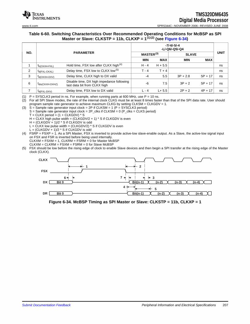
Bit 0 Bit(n-1) (n-2) (n-3) (n-4)
Bit 0 Bit(n-1) (n-2) (n-3) (n-4)5
4
376
21
CLKX
FSX
DX
DR
TMS320DM6435Digital Media Processor
www.ti.com SPRS344C–NOVEMBER 2006–REVISED JUNE 2008
Table 6-60. Switching Characteristics Over Recommended Operating Conditions for McBSP as SPIMaster or Slave: CLKSTP = 11b, CLKXP = 1 (1) (2) (see Figure 6-34)
-7/-6/-5/-4-L/-Q6/-Q5/-Q4
NO. PARAMETER UNITMASTER (3) SLAVEMIN MAX MIN MAX
1 th(CKXH-FXL) Hold time, FSX low after CLKX high (4) H - 4 H + 5.5 ns2 td(FXL-CKXL) Delay time, FSX low to CLKX low (5) T - 4 T + 4 ns3 td(CKXH-DXV) Delay time, CLKX high to DX valid -4 5.5 3P + 2.8 5P + 17 ns
Disable time, DX high impedance following6 tdis(CKXH-DXHZ) -6 7.5 3P + 2 5P + 17 nslast data bit from CLKX high7 td(FXL-DXV) Delay time, FSX low to DX valid L - 4 L+ 5.5 2P + 2 4P + 17 ns
(1) P = SYSCLK3 period in ns. For example, when running parts at 600 MHz, use P = 10 ns.(2) For all SPI Slave modes, the rate of the internal clock CLKG must be at least 8 times faster than that of the SPI data rate. User should
program sample rate generator to achieve maximum CLKG by setting CLKSM = CLKGDV = 1.(3) S = Sample rate generator input clock = 2P if CLKSM = 1 (P = SYSCLK3 period)
S = Sample rate generator input clock = 2P_clks if CLKSM = 0 (P_clks = CLKS period)T = CLKX period = (1 + CLKGDV) * SH = CLKX high pulse width = (CLKGDV/2 + 1) * S if CLKGDV is evenH = (CLKGDV + 1)/2 * S if CLKGDV is oddL = CLKX low pulse width = (CLKGDV/2) * S if CLKGDV is evenL = (CLKGDV + 1)/2 * S if CLKGDV is odd
(4) FSRP = FSXP = 1. As a SPI Master, FSX is inverted to provide active-low slave-enable output. As a Slave, the active-low signal inputon FSX and FSR is inverted before being used internally.CLKXM = FSXM = 1, CLKRM = FSRM = 0 for Master McBSPCLKXM = CLKRM = FSXM = FSRM = 0 for Slave McBSP
(5) FSX should be low before the rising edge of clock to enable Slave devices and then begin a SPI transfer at the rising edge of the Masterclock (CLKX).
Figure 6-34. McBSP Timing as SPI Master or Slave: CLKSTP = 11b, CLKXP = 1
Submit Documentation Feedback Peripheral Information and Electrical Specifications 207
6.15 Multichannel Audio Serial Port (McASP0) Peripheral
6.15.1 McASP0 Device-Specific Information
TMS320DM6435Digital Media ProcessorSPRS344C–NOVEMBER 2006–REVISED JUNE 2008 www.ti.com
The McASP functions as a general-purpose audio serial port optimized for the needs of multichannelaudio applications. The McASP is useful for time-division multiplexed (TDM) stream, Inter-IntegratedSound (I2S) protocols, and intercomponent digital audio interface transmission (DIT).
The DM6435 device includes one multichannel audio serial port (McASP) interface peripheral (McASP0).The McASP0 is a serial port optimized for the needs of multichannel audio applications.
The McASP0 consists of a transmit and receive section. These sections can operate completelyindependently with different data formats, separate master clocks, bit clocks, and frame syncs oralternatively, the transmit and receive sections may be synchronized. The McASP module also includes apool of 16 shift registers that may be configured to operate as either transmit data or receive data.
The transmit section of the McASP can transmit data in either a time-division-multiplexed (TDM)synchronous serial format or in a digital audio interface (DIT) format where the bit stream is encoded forS/PDIF, AES-3, IEC-60958, CP-430 transmission. The receive section of the McASP supports the TDMsynchronous serial format.
The McASP can support one transmit data format (either a TDM format or DIT format) and one receiveformat at a time. All transmit shift registers use the same format and all receive shift registers use thesame format. However, the transmit and receive formats need not be the same.
Both the transmit and receive sections of the McASP also support burst mode which is useful fornon-audio data (for example, passing control information between two DSPs).
The McASP peripheral has additional capability for flexible clock generation, and error detection/handling,as well as error management.
For more detailed information on and the functionality of the McASP0 peripheral, see the TMS320DM643xDMP Multichannel Audio Serial Port (McASP) User's Guide (literature number SPRU980).
Peripheral Information and Electrical Specifications208 Submit Documentation Feedback
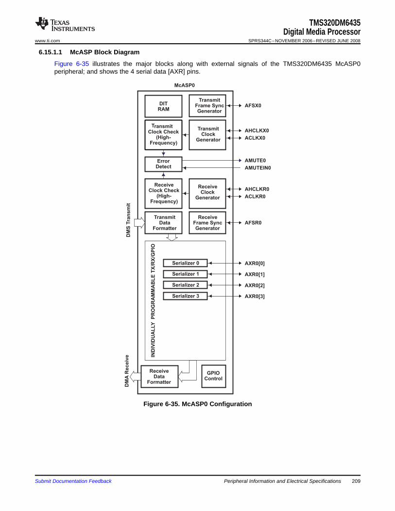
6.15.1.1 McASP Block Diagram
ReceiveClock
Generator
AHCLKR0
ACLKR0
T
GeneratorClock
Transmit
ACLKX0
AHCLKX0
DITRAM
Transmit
GeneratorFrame Sync AFSX0
DetectError
ReceiveFrame SyncGeneratorFormatter
TransmitData
AMUTE0
AMUTEIN0
AFSR0
Serializer 0
Serializer 1
Serializer 3
Serializer 2
Clock Checkransmit
(High-Frequency)
ReceiveClock Check
(High-Frequency)
Receive
FormatterData
McASP0
DM
S T
ran
sm
itD
MA
Re
ce
ive IN
DIV
IDU
AL
LY
PR
OG
RA
MM
AB
LE
TX
/RX
/GP
IO
ControlGPIO
AXR0[0]
AXR0[1]
AXR0[3]
AXR0[2]
TMS320DM6435Digital Media Processor
www.ti.com SPRS344C–NOVEMBER 2006–REVISED JUNE 2008
Figure 6-35 illustrates the major blocks along with external signals of the TMS320DM6435 McASP0peripheral; and shows the 4 serial data [AXR] pins.
Figure 6-35. McASP0 Configuration
Submit Documentation Feedback Peripheral Information and Electrical Specifications 209
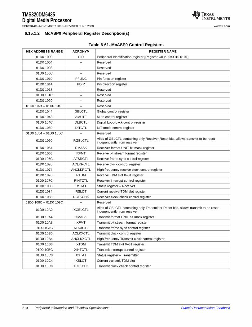
6.15.1.2 McASP0 Peripheral Register Description(s)
TMS320DM6435Digital Media ProcessorSPRS344C–NOVEMBER 2006–REVISED JUNE 2008 www.ti.com
Table 6-61. McASP0 Control RegistersHEX ADDRESS RANGE ACRONYM REGISTER NAME
01D0 1000 PID Peripheral Identification register [Register value: 0x0010 0101]01D0 1004 – Reserved01D0 1008 – Reserved01D0 100C – Reserved01D0 1010 PFUNC Pin function register01D0 1014 PDIR Pin direction register01D0 1018 – Reserved01D0 101C – Reserved01D0 1020 – Reserved
01D0 1024 – 01D0 1040 – Reserved01D0 1044 GBLCTL Global control register01D0 1048 AMUTE Mute control register01D0 104C DLBCTL Digital Loop-back control register01D0 1050 DITCTL DIT mode control register
01D0 1054 – 01D0 105C – ReservedAlias of GBLCTL containing only Receiver Reset bits, allows transmit to be reset01D0 1060 RGBLCTL independently from receive.
01D0 1064 RMASK Receiver format UNIT bit mask register01D0 1068 RFMT Receive bit stream format register01D0 106C AFSRCTL Receive frame sync control register01D0 1070 ACLKRCTL Receive clock control register01D0 1074 AHCLKRCTL High-frequency receive clock control register01D0 1078 RTDM Receive TDM slot 0–31 register01D0 107C RINTCTL Receiver interrupt control register01D0 1080 RSTAT Status register – Receiver01D0 1084 RSLOT Current receive TDM slot register01D0 1088 RCLKCHK Receiver clock check control register
01D0 108C – 01D0 109C – ReservedAlias of GBLCTL containing only Transmitter Reset bits, allows transmit to be reset01D0 10A0 XGBLCTL independently from receive.
01D0 10A4 XMASK Transmit format UNIT bit mask register01D0 10A8 XFMT Transmit bit stream format register01D0 10AC AFSXCTL Transmit frame sync control register01D0 10B0 ACLKXCTL Transmit clock control register01D0 10B4 AHCLKXCTL High-frequency Transmit clock control register01D0 10B8 XTDM Transmit TDM slot 0–31 register01D0 10BC XINTCTL Transmit interrupt control register01D0 10C0 XSTAT Status register – Transmitter01D0 10C4 XSLOT Current transmit TDM slot01D0 10C8 XCLKCHK Transmit clock check control register
210 Peripheral Information and Electrical Specifications Submit Documentation Feedback
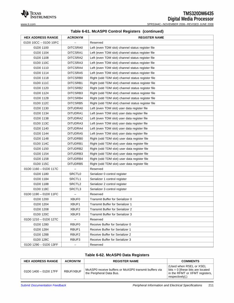
TMS320DM6435Digital Media Processor
www.ti.com SPRS344C–NOVEMBER 2006–REVISED JUNE 2008
Table 6-61. McASP0 Control Registers (continued)HEX ADDRESS RANGE ACRONYM REGISTER NAME01D0 10CC – 01D0 10FC – Reserved
01D0 1100 DITCSRA0 Left (even TDM slot) channel status register file01D0 1104 DITCSRA1 Left (even TDM slot) channel status register file01D0 1108 DITCSRA2 Left (even TDM slot) channel status register file01D0 110C DITCSRA3 Left (even TDM slot) channel status register file01D0 1110 DITCSRA4 Left (even TDM slot) channel status register file01D0 1114 DITCSRA5 Left (even TDM slot) channel status register file01D0 1118 DITCSRB0 Right (odd TDM slot) channel status register file01D0 111C DITCSRB1 Right (odd TDM slot) channel status register file01D0 1120 DITCSRB2 Right (odd TDM slot) channel status register file01D0 1124 DITCSRB3 Right (odd TDM slot) channel status register file01D0 1128 DITCSRB4 Right (odd TDM slot) channel status register file01D0 112C DITCSRB5 Right (odd TDM slot) channel status register file01D0 1130 DITUDRA0 Left (even TDM slot) user data register file01D0 1134 DITUDRA1 Left (even TDM slot) user data register file01D0 1138 DITUDRA2 Left (even TDM slot) user data register file01D0 113C DITUDRA3 Left (even TDM slot) user data register file01D0 1140 DITUDRA4 Left (even TDM slot) user data register file01D0 1144 DITUDRA5 Left (even TDM slot) user data register file01D0 1148 DITUDRB0 Right (odd TDM slot) user data register file01D0 114C DITUDRB1 Right (odd TDM slot) user data register file01D0 1150 DITUDRB2 Right (odd TDM slot) user data register file01D0 1154 DITUDRB3 Right (odd TDM slot) user data register file01D0 1158 DITUDRB4 Right (odd TDM slot) user data register file01D0 115C DITUDRB5 Right (odd TDM slot) user data register file
01D0 1160 – 01D0 117C – Reserved01D0 1180 SRCTL0 Serializer 0 control register01D0 1184 SRCTL1 Serializer 1 control register01D0 1188 SRCTL2 Serializer 2 control register01D0 118C SRCTL3 Serializer 3 control register
01D0 1190 – 01D0 11FC – Reserved01D0 1200 XBUF0 Transmit Buffer for Serializer 001D0 1204 XBUF1 Transmit Buffer for Serializer 101D0 1208 XBUF2 Transmit Buffer for Serializer 201D0 120C XBUF3 Transmit Buffer for Serializer 3
01D0 1210 – 01D0 127C – Reserved01D0 1280 RBUF0 Receive Buffer for Serializer 001D0 1284 RBUF1 Receive Buffer for Serializer 101D0 1288 RBUF2 Receive Buffer for Serializer 201D0 128C RBUF3 Receive Buffer for Serializer 3
01D0 1290 – 01D0 13FF – Reserved
Table 6-62. McASP0 Data RegistersHEX ADDRESS RANGE ACRONYM REGISTER NAME COMMENTS
(Used when RSEL or XSELMcASP0 receive buffers or McASP0 transmit buffers via bits = 0 [these bits are located01D0 1400 – 01D0 17FF RBUF/XBUF the Peripheral Data Bus. in the RFMT or XFMT registers,
respectively].)
Submit Documentation Feedback Peripheral Information and Electrical Specifications 211
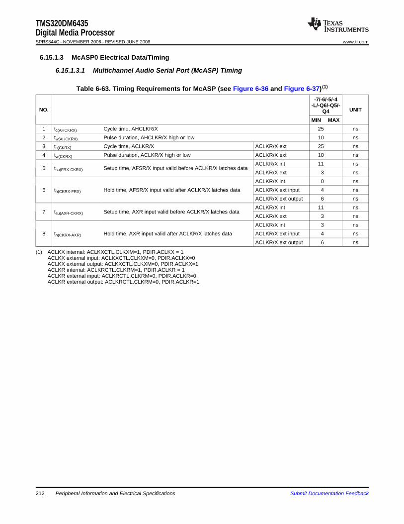
6.15.1.3 McASP0 Electrical Data/Timing
TMS320DM6435Digital Media ProcessorSPRS344C–NOVEMBER 2006–REVISED JUNE 2008 www.ti.com
6.15.1.3.1 Multichannel Audio Serial Port (McASP) Timing
Table 6-63. Timing Requirements for McASP (see Figure 6-36 and Figure 6-37) (1)
-7/-6/-5/-4-L/-Q6/-Q5/-
NO. UNITQ4MIN MAX
1 tc(AHCKRX) Cycle time, AHCLKR/X 25 ns2 tw(AHCKRX) Pulse duration, AHCLKR/X high or low 10 ns3 tc(CKRX) Cycle time, ACLKR/X ACLKR/X ext 25 ns4 tw(CKRX) Pulse duration, ACLKR/X high or low ACLKR/X ext 10 ns
ACLKR/X int 11 ns5 tsu(FRX-CKRX) Setup time, AFSR/X input valid before ACLKR/X latches data
ACLKR/X ext 3 nsACLKR/X int 0 ns
6 th(CKRX-FRX) Hold time, AFSR/X input valid after ACLKR/X latches data ACLKR/X ext input 4 nsACLKR/X ext output 6 nsACLKR/X int 11 ns
7 tsu(AXR-CKRX) Setup time, AXR input valid before ACLKR/X latches dataACLKR/X ext 3 nsACLKR/X int 3 ns
8 th(CKRX-AXR) Hold time, AXR input valid after ACLKR/X latches data ACLKR/X ext input 4 nsACLKR/X ext output 6 ns
(1) ACLKX internal: ACLKXCTL.CLKXM=1, PDIR.ACLKX = 1ACLKX external input: ACLKXCTL.CLKXM=0, PDIR.ACLKX=0ACLKX external output: ACLKXCTL.CLKXM=0, PDIR.ACLKX=1ACLKR internal: ACLKRCTL.CLKRM=1, PDIR.ACLKR = 1ACLKR external input: ACLKRCTL.CLKRM=0, PDIR.ACLKR=0ACLKR external output: ACLKRCTL.CLKRM=0, PDIR.ACLKR=1
Peripheral Information and Electrical Specifications212 Submit Documentation Feedback
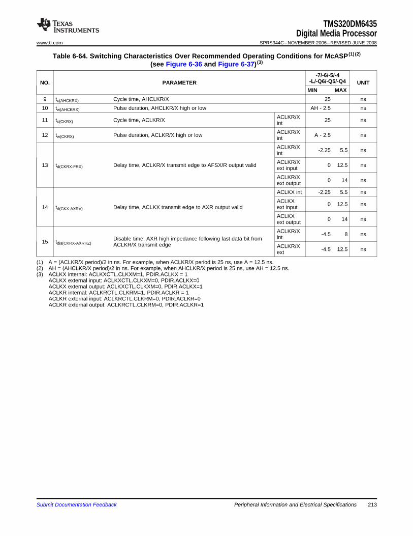
TMS320DM6435Digital Media Processor
www.ti.com SPRS344C–NOVEMBER 2006–REVISED JUNE 2008
Table 6-64. Switching Characteristics Over Recommended Operating Conditions for McASP (1) (2)
(see Figure 6-36 and Figure 6-37) (3)
-7/-6/-5/-4-L/-Q6/-Q5/-Q4NO. PARAMETER UNIT
MIN MAX9 tc(AHCKRX) Cycle time, AHCLKR/X 25 ns10 tw(AHCKRX) Pulse duration, AHCLKR/X high or low AH - 2.5 ns
ACLKR/X11 tc(CKRX) Cycle time, ACLKR/X 25 nsintACLKR/X12 tw(CKRX) Pulse duration, ACLKR/X high or low A - 2.5 nsintACLKR/X -2.25 5.5 nsintACLKR/X13 td(CKRX-FRX) Delay time, ACLKR/X transmit edge to AFSX/R output valid 0 12.5 nsext inputACLKR/X 0 14 nsext outputACLKX int -2.25 5.5 nsACLKX 0 12.5 ns14 td(CKX-AXRV) Delay time, ACLKX transmit edge to AXR output valid ext inputACLKX 0 14 nsext outputACLKR/X -4.5 8 nsintDisable time, AXR high impedance following last data bit from15 tdis(CKRX-AXRHZ) ACLKR/X transmit edge ACLKR/X -4.5 12.5 nsext
(1) A = (ACLKR/X period)/2 in ns. For example, when ACLKR/X period is 25 ns, use A = 12.5 ns.(2) AH = (AHCLKR/X period)/2 in ns. For example, when AHCLKR/X period is 25 ns, use AH = 12.5 ns.(3) ACLKX internal: ACLKXCTL.CLKXM=1, PDIR.ACLKX = 1
ACLKX external input: ACLKXCTL.CLKXM=0, PDIR.ACLKX=0ACLKX external output: ACLKXCTL.CLKXM=0, PDIR.ACLKX=1ACLKR internal: ACLKRCTL.CLKRM=1, PDIR.ACLKR = 1ACLKR external input: ACLKRCTL.CLKRM=0, PDIR.ACLKR=0ACLKR external output: ACLKRCTL.CLKRM=0, PDIR.ACLKR=1
Submit Documentation Feedback Peripheral Information and Electrical Specifications 213
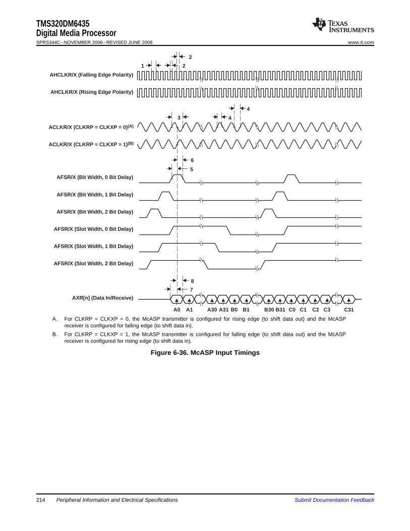
8
7
4
43
2
21
A0 A1 B0 B1A30 A31 B30 B31 C0 C1 C2 C3 C31
AHCLKR/X (Falling Edge Polarity)
AHCLKR/X (Rising Edge Polarity)
AFSR/X (Bit Width, 0 Bit Delay)
AFSR/X (Bit Width, 1 Bit Delay)
AFSR/X (Bit Width, 2 Bit Delay)
AFSR/X (Slot Width, 0 Bit Delay)
AFSR/X (Slot Width, 1 Bit Delay)
AFSR/X (Slot Width, 2 Bit Delay)
AXR[n] (Data In/Receive)
6
5
ACLKR/X (CLKRP = CLKXP = 0)(A)
ACLKR/X (CLKRP = CLKXP = 1)(B)
TMS320DM6435Digital Media ProcessorSPRS344C–NOVEMBER 2006–REVISED JUNE 2008 www.ti.com
A. For CLKRP = CLKXP = 0, the McASP transmitter is configured for rising edge (to shift data out) and the McASPreceiver is configured for falling edge (to shift data in).
B. For CLKRP = CLKXP = 1, the McASP transmitter is configured for falling edge (to shift data out) and the McASPreceiver is configured for rising edge (to shift data in).
Figure 6-36. McASP Input Timings
214 Peripheral Information and Electrical Specifications Submit Documentation Feedback

1514
131313
1313
1313
12
1211
1010
9
A0 A1 B0 B1A30 A31 B30 B31 C0 C1 C2 C3 C31
AHCLKR/X (Falling Edge Polarity)
AHCLKR/X (Rising Edge Polarity)
AFSR/X (Bit Width, 0 Bit Delay)
AFSR/X (Bit Width, 1 Bit Delay)
AFSR/X (Bit Width, 2 Bit Delay)
AFSR/X (Slot Width, 0 Bit Delay)
AFSR/X (Slot Width, 1 Bit Delay)
AFSR/X (Slot Width, 2 Bit Delay)
AXR[n] (Data Out/Transmit)
ACLKR/X (CLKRP = CLKXP = 0)(B)
ACLKR/X (CLKRP = CLKXP = 1)(A)
TMS320DM6435Digital Media Processor
www.ti.com SPRS344C–NOVEMBER 2006–REVISED JUNE 2008
A. For CLKRP = CLKXP = 1, the McASP transmitter is configured for falling edge (to shift data out) and the McASPreceiver is configured for rising edge (to shift data in).
B. For CLKRP = CLKXP = 0, the McASP transmitter is configured for rising edge (to shift data out) and the McASPreceiver is configured for falling edge (to shift data in).
Figure 6-37. McASP Output Timings
Submit Documentation Feedback Peripheral Information and Electrical Specifications 215
6.16 High-End Controller Area Network Controller (HECC)
6.16.1 HECC Device-Specific Information
TMS320DM6435Digital Media ProcessorSPRS344C–NOVEMBER 2006–REVISED JUNE 2008 www.ti.com
The DM6435 device has a High-End Controller Area Network Controllers (HECC). The HECC usesestablished protocol to communicate serially with other controllers in harsh environments. The HECC isfully compliant with the Controller Area Network (CAN) protocol, version 2.0B.
Key features of the HECC include the following:• CAN, version 2.0B compliant• 32 RX/TX message objects• 32 receive identifier masks• Programmable wake-up on bus activity• Programmable interrupt scheme• Automatic reply to a remote request• Automatic re-transmission in case of error or loss of arbitration• Protection against reception of a new message• 32-bit time stamp• Local network time counter• Programmable priority register for each message• Programmable transmission and reception time-out• HECC/SCC mode of operation• Standard-Extended Identifier• Self-test mode
For more details on the HECC, see the TMS320DM643x High-End CAN Controller (HECC) User's Guide(literature number SPRU981).
Software must not access "Reserved" locations of the HECC. Access to HECC "Reserved" locations mayhang the device.
216 Peripheral Information and Electrical Specifications Submit Documentation Feedback
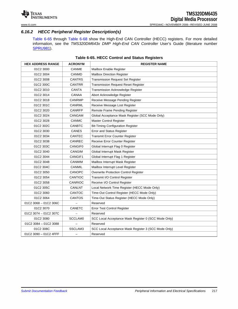
6.16.2 HECC Peripheral Register Description(s)
TMS320DM6435Digital Media Processor
www.ti.com SPRS344C–NOVEMBER 2006–REVISED JUNE 2008
Table 6-65 through Table 6-68 show the High-End CAN Controller (HECC) registers. For more detailedinformation, see the TMS320DM643x DMP High-End CAN Controller User’s Guide (literature numberSPRU981).
Table 6-65. HECC Control and Status RegistersHEX ADDRESS RANGE ACRONYM REGISTER NAME
01C2 3000 CANME Mailbox Enable Register01C2 3004 CANMD Mailbox Direction Register01C2 3008 CANTRS Transmission Request Set Register01C2 300C CANTRR Transmission Request Reset Register01C2 3010 CANTA Transmission Acknowledge Register01C2 3014 CANAA Abort Acknowledge Register01C2 3018 CANRMP Receive Message Pending Register01C2 301C CANRML Receive Message Lost Register01C2 3020 CANRFP Remote Frame Pending Register01C2 3024 CANGAM Global Acceptance Mask Register (SCC Mode Only)01C2 3028 CANMC Master Control Register01C2 302C CANBTC Bit-Timing Configuration Register01C2 3030 CANES Error and Status Register01C2 3034 CANTEC Transmit Error Counter Register01C2 3038 CANREC Receive Error Counter Register01C2 303C CANGIF0 Global Interrupt Flag 0 Register01C2 3040 CANGIM Global Interrupt Mask Register01C2 3044 CANGIF1 Global Interrupt Flag 1 Register01C2 3048 CANMIM Mailbox Interrupt Mask Register01C2 304C CANMIL Mailbox Interrupt Level Register01C2 3050 CANOPC Overwrite Protection Control Register01C2 3054 CANTIOC Transmit I/O Control Register01C2 3058 CANRIOC Receive I/O Control Register01C2 305C CANLNT Local Network Time Register (HECC Mode Only)01C2 3060 CANTOC Time-Out Control Register (HECC Mode Only)01C2 3064 CANTOS Time-Out Status Register (HECC Mode Only)
01C2 3068 – 01C2 306C – Reserved01C2 3070 CANETC Error Test Control Register
01C2 3074 – 01C2 307C – Reserved01C2 3080 SCCLAM0 SCC Local Acceptance Mask Register 0 (SCC Mode Only)
01C2 3084 – 01C2 3088 – Reserved01C2 308C SSCLAM3 SCC Local Acceptance Mask Register 3 (SCC Mode Only)
01C2 3090 – 01C2 4FFF – Reserved
Submit Documentation Feedback Peripheral Information and Electrical Specifications 217
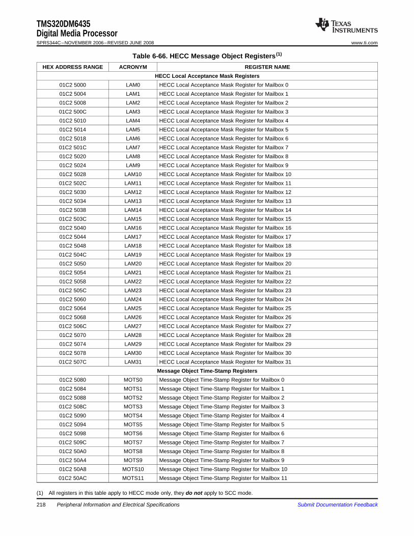
TMS320DM6435Digital Media ProcessorSPRS344C–NOVEMBER 2006–REVISED JUNE 2008 www.ti.com
Table 6-66. HECC Message Object Registers (1)
HEX ADDRESS RANGE ACRONYM REGISTER NAMEHECC Local Acceptance Mask Registers
01C2 5000 LAM0 HECC Local Acceptance Mask Register for Mailbox 001C2 5004 LAM1 HECC Local Acceptance Mask Register for Mailbox 101C2 5008 LAM2 HECC Local Acceptance Mask Register for Mailbox 201C2 500C LAM3 HECC Local Acceptance Mask Register for Mailbox 301C2 5010 LAM4 HECC Local Acceptance Mask Register for Mailbox 401C2 5014 LAM5 HECC Local Acceptance Mask Register for Mailbox 501C2 5018 LAM6 HECC Local Acceptance Mask Register for Mailbox 601C2 501C LAM7 HECC Local Acceptance Mask Register for Mailbox 701C2 5020 LAM8 HECC Local Acceptance Mask Register for Mailbox 801C2 5024 LAM9 HECC Local Acceptance Mask Register for Mailbox 901C2 5028 LAM10 HECC Local Acceptance Mask Register for Mailbox 1001C2 502C LAM11 HECC Local Acceptance Mask Register for Mailbox 1101C2 5030 LAM12 HECC Local Acceptance Mask Register for Mailbox 1201C2 5034 LAM13 HECC Local Acceptance Mask Register for Mailbox 1301C2 5038 LAM14 HECC Local Acceptance Mask Register for Mailbox 1401C2 503C LAM15 HECC Local Acceptance Mask Register for Mailbox 1501C2 5040 LAM16 HECC Local Acceptance Mask Register for Mailbox 1601C2 5044 LAM17 HECC Local Acceptance Mask Register for Mailbox 1701C2 5048 LAM18 HECC Local Acceptance Mask Register for Mailbox 1801C2 504C LAM19 HECC Local Acceptance Mask Register for Mailbox 1901C2 5050 LAM20 HECC Local Acceptance Mask Register for Mailbox 2001C2 5054 LAM21 HECC Local Acceptance Mask Register for Mailbox 2101C2 5058 LAM22 HECC Local Acceptance Mask Register for Mailbox 2201C2 505C LAM23 HECC Local Acceptance Mask Register for Mailbox 2301C2 5060 LAM24 HECC Local Acceptance Mask Register for Mailbox 2401C2 5064 LAM25 HECC Local Acceptance Mask Register for Mailbox 2501C2 5068 LAM26 HECC Local Acceptance Mask Register for Mailbox 2601C2 506C LAM27 HECC Local Acceptance Mask Register for Mailbox 2701C2 5070 LAM28 HECC Local Acceptance Mask Register for Mailbox 2801C2 5074 LAM29 HECC Local Acceptance Mask Register for Mailbox 2901C2 5078 LAM30 HECC Local Acceptance Mask Register for Mailbox 3001C2 507C LAM31 HECC Local Acceptance Mask Register for Mailbox 31
Message Object Time-Stamp Registers01C2 5080 MOTS0 Message Object Time-Stamp Register for Mailbox 001C2 5084 MOTS1 Message Object Time-Stamp Register for Mailbox 101C2 5088 MOTS2 Message Object Time-Stamp Register for Mailbox 201C2 508C MOTS3 Message Object Time-Stamp Register for Mailbox 301C2 5090 MOTS4 Message Object Time-Stamp Register for Mailbox 401C2 5094 MOTS5 Message Object Time-Stamp Register for Mailbox 501C2 5098 MOTS6 Message Object Time-Stamp Register for Mailbox 601C2 509C MOTS7 Message Object Time-Stamp Register for Mailbox 701C2 50A0 MOTS8 Message Object Time-Stamp Register for Mailbox 801C2 50A4 MOTS9 Message Object Time-Stamp Register for Mailbox 901C2 50A8 MOTS10 Message Object Time-Stamp Register for Mailbox 1001C2 50AC MOTS11 Message Object Time-Stamp Register for Mailbox 11
(1) All registers in this table apply to HECC mode only, they do not apply to SCC mode.
Peripheral Information and Electrical Specifications218 Submit Documentation Feedback
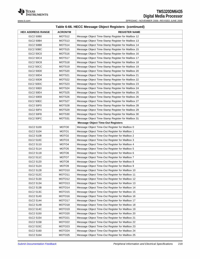
TMS320DM6435Digital Media Processor
www.ti.com SPRS344C–NOVEMBER 2006–REVISED JUNE 2008
Table 6-66. HECC Message Object Registers (continued)HEX ADDRESS RANGE ACRONYM REGISTER NAME
01C2 50B0 MOTS12 Message Object Time-Stamp Register for Mailbox 1201C2 50B4 MOTS13 Message Object Time-Stamp Register for Mailbox 1301C2 50B8 MOTS14 Message Object Time-Stamp Register for Mailbox 1401C2 50BC MOTS15 Message Object Time-Stamp Register for Mailbox 1501C2 50C0 MOTS16 Message Object Time-Stamp Register for Mailbox 1601C2 50C4 MOTS17 Message Object Time-Stamp Register for Mailbox 1701C2 50C8 MOTS18 Message Object Time-Stamp Register for Mailbox 1801C2 50CC MOTS19 Message Object Time-Stamp Register for Mailbox 1901C2 50D0 MOTS20 Message Object Time-Stamp Register for Mailbox 2001C2 50D4 MOTS21 Message Object Time-Stamp Register for Mailbox 2101C2 50D8 MOTS22 Message Object Time-Stamp Register for Mailbox 2201C2 50DC MOTS23 Message Object Time-Stamp Register for Mailbox 2301C2 50E0 MOTS24 Message Object Time-Stamp Register for Mailbox 2401C2 50E4 MOTS25 Message Object Time-Stamp Register for Mailbox 2501C2 50E8 MOTS26 Message Object Time-Stamp Register for Mailbox 2601C2 50EC MOTS27 Message Object Time-Stamp Register for Mailbox 2701C2 50F0 MOTS28 Message Object Time-Stamp Register for Mailbox 2801C2 50F4 MOTS29 Message Object Time-Stamp Register for Mailbox 2901C2 50F8 MOTS30 Message Object Time-Stamp Register for Mailbox 3001C2 50FC MOTS31 Message Object Time-Stamp Register for Mailbox 31
Message Object Time-Out Registers01C2 5100 MOTO0 Message Object Time-Out Register for Mailbox 001C2 5104 MOTO1 Message Object Time-Out Register for Mailbox 101C2 5108 MOTO2 Message Object Time-Out Register for Mailbox 201C2 510C MOTO3 Message Object Time-Out Register for Mailbox 301C2 5110 MOTO4 Message Object Time-Out Register for Mailbox 401C2 5114 MOTO5 Message Object Time-Out Register for Mailbox 501C2 5118 MOTO6 Message Object Time-Out Register for Mailbox 601C2 511C MOTO7 Message Object Time-Out Register for Mailbox 701C2 5120 MOTO8 Message Object Time-Out Register for Mailbox 801C2 5124 MOTO9 Message Object Time-Out Register for Mailbox 901C2 5128 MOTO10 Message Object Time-Out Register for Mailbox 1001C2 512C MOTO11 Message Object Time-Out Register for Mailbox 1101C2 5130 MOTO12 Message Object Time-Out Register for Mailbox 1201C2 5134 MOTO13 Message Object Time-Out Register for Mailbox 1301C2 5138 MOTO14 Message Object Time-Out Register for Mailbox 1401C2 513C MOTO15 Message Object Time-Out Register for Mailbox 1501C2 5140 MOTO16 Message Object Time-Out Register for Mailbox 1601C2 5144 MOTO17 Message Object Time-Out Register for Mailbox 1701C2 5148 MOTO18 Message Object Time-Out Register for Mailbox 1801C2 514C MOTO19 Message Object Time-Out Register for Mailbox 1901C2 5150 MOTO20 Message Object Time-Out Register for Mailbox 2001C2 5154 MOTO21 Message Object Time-Out Register for Mailbox 2101C2 5158 MOTO22 Message Object Time-Out Register for Mailbox 2201C2 515C MOTO23 Message Object Time-Out Register for Mailbox 2301C2 5160 MOTO24 Message Object Time-Out Register for Mailbox 2401C2 5164 MOTO25 Message Object Time-Out Register for Mailbox 25
Submit Documentation Feedback Peripheral Information and Electrical Specifications 219
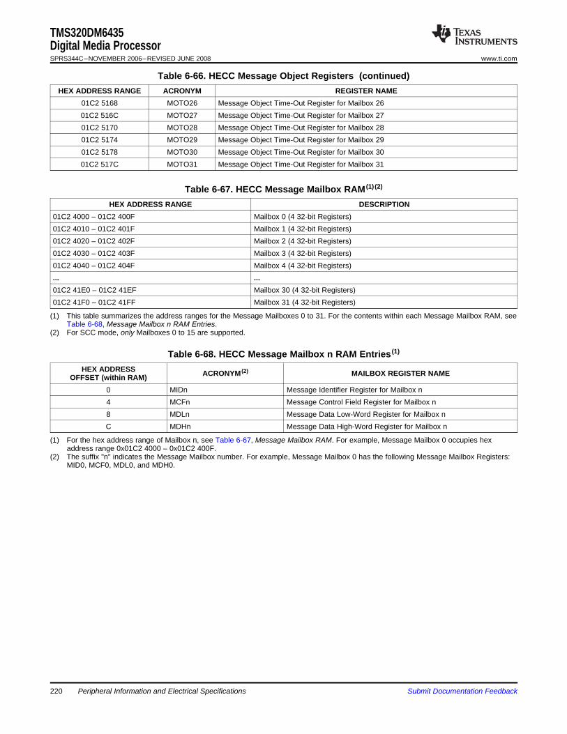
TMS320DM6435Digital Media ProcessorSPRS344C–NOVEMBER 2006–REVISED JUNE 2008 www.ti.com
Table 6-66. HECC Message Object Registers (continued)HEX ADDRESS RANGE ACRONYM REGISTER NAME
01C2 5168 MOTO26 Message Object Time-Out Register for Mailbox 2601C2 516C MOTO27 Message Object Time-Out Register for Mailbox 2701C2 5170 MOTO28 Message Object Time-Out Register for Mailbox 2801C2 5174 MOTO29 Message Object Time-Out Register for Mailbox 2901C2 5178 MOTO30 Message Object Time-Out Register for Mailbox 3001C2 517C MOTO31 Message Object Time-Out Register for Mailbox 31
Table 6-67. HECC Message Mailbox RAM (1) (2)
HEX ADDRESS RANGE DESCRIPTION01C2 4000 – 01C2 400F Mailbox 0 (4 32-bit Registers)01C2 4010 – 01C2 401F Mailbox 1 (4 32-bit Registers)01C2 4020 – 01C2 402F Mailbox 2 (4 32-bit Registers)01C2 4030 – 01C2 403F Mailbox 3 (4 32-bit Registers)01C2 4040 – 01C2 404F Mailbox 4 (4 32-bit Registers)... ...01C2 41E0 – 01C2 41EF Mailbox 30 (4 32-bit Registers)01C2 41F0 – 01C2 41FF Mailbox 31 (4 32-bit Registers)
(1) This table summarizes the address ranges for the Message Mailboxes 0 to 31. For the contents within each Message Mailbox RAM, seeTable 6-68, Message Mailbox n RAM Entries.
(2) For SCC mode, only Mailboxes 0 to 15 are supported.
Table 6-68. HECC Message Mailbox n RAM Entries (1)
HEX ADDRESS ACRONYM (2) MAILBOX REGISTER NAMEOFFSET (within RAM)0 MIDn Message Identifier Register for Mailbox n4 MCFn Message Control Field Register for Mailbox n8 MDLn Message Data Low-Word Register for Mailbox nC MDHn Message Data High-Word Register for Mailbox n
(1) For the hex address range of Mailbox n, see Table 6-67, Message Mailbox RAM. For example, Message Mailbox 0 occupies hexaddress range 0x01C2 4000 – 0x01C2 400F.
(2) The suffix "n" indicates the Message Mailbox number. For example, Message Mailbox 0 has the following Message Mailbox Registers:MID0, MCF0, MDL0, and MDH0.
Peripheral Information and Electrical Specifications220 Submit Documentation Feedback
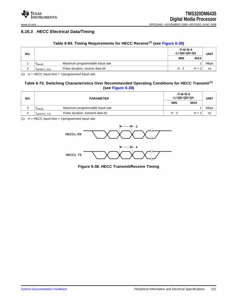
6.16.3 HECC Electrical Data/Timing
2
HECCx_RX
4
HECCx_TX
TMS320DM6435Digital Media Processor
www.ti.com SPRS344C–NOVEMBER 2006–REVISED JUNE 2008
Table 6-69. Timing Requirements for HECC Receive (1) (see Figure 6-38)-7/-6/-5/-4
-L/-Q6/-Q5/-Q4NO. UNITMIN MAX
1 f(baud) Maximum programmable baud rate 1 Mbps2 tw(HECC_RX) Pulse duration, receive data bit H - 2 H + 2 ns
(1) H = HECC baud time = 1/programmed baud rate.
Table 6-70. Switching Characteristics Over Recommended Operating Conditions for HECC Transmit (1)
(see Figure 6-38)-7/-6/-5/-4
-L/-Q6/-Q5/-Q4NO. PARAMETER UNITMIN MAX
3 f(baud) Maximum programmable baud rate 1 Mbps4 tw(HECC_TX) Pulse duration, transmit data bit H - 2 H + 2 ns
(1) H = HECC baud time = 1/programmed baud rate.
Figure 6-38. HECC Transmit/Receive Timing
Submit Documentation Feedback Peripheral Information and Electrical Specifications 221
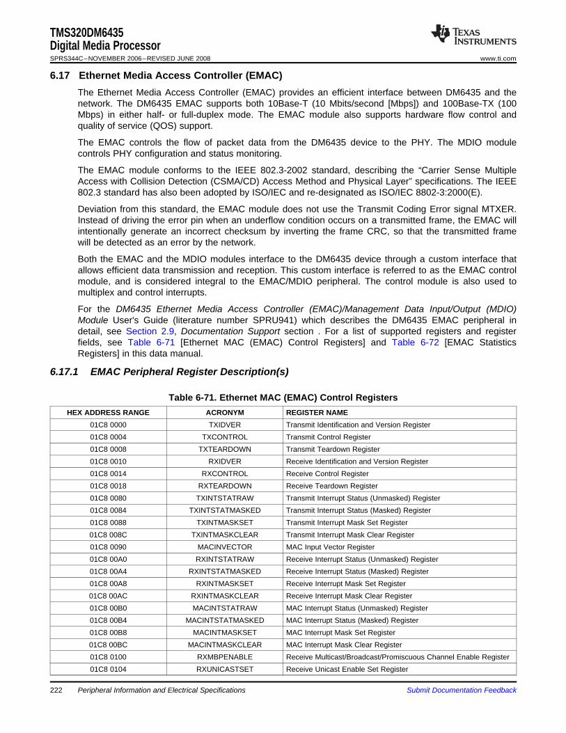
6.17 Ethernet Media Access Controller (EMAC)
6.17.1 EMAC Peripheral Register Description(s)
TMS320DM6435Digital Media ProcessorSPRS344C–NOVEMBER 2006–REVISED JUNE 2008 www.ti.com
The Ethernet Media Access Controller (EMAC) provides an efficient interface between DM6435 and thenetwork. The DM6435 EMAC supports both 10Base-T (10 Mbits/second [Mbps]) and 100Base-TX (100Mbps) in either half- or full-duplex mode. The EMAC module also supports hardware flow control andquality of service (QOS) support.
The EMAC controls the flow of packet data from the DM6435 device to the PHY. The MDIO modulecontrols PHY configuration and status monitoring.
The EMAC module conforms to the IEEE 802.3-2002 standard, describing the “Carrier Sense MultipleAccess with Collision Detection (CSMA/CD) Access Method and Physical Layer” specifications. The IEEE802.3 standard has also been adopted by ISO/IEC and re-designated as ISO/IEC 8802-3:2000(E).
Deviation from this standard, the EMAC module does not use the Transmit Coding Error signal MTXER.Instead of driving the error pin when an underflow condition occurs on a transmitted frame, the EMAC willintentionally generate an incorrect checksum by inverting the frame CRC, so that the transmitted framewill be detected as an error by the network.
Both the EMAC and the MDIO modules interface to the DM6435 device through a custom interface thatallows efficient data transmission and reception. This custom interface is referred to as the EMAC controlmodule, and is considered integral to the EMAC/MDIO peripheral. The control module is also used tomultiplex and control interrupts.
For the DM6435 Ethernet Media Access Controller (EMAC)/Management Data Input/Output (MDIO)Module User's Guide (literature number SPRU941) which describes the DM6435 EMAC peripheral indetail, see Section 2.9, Documentation Support section . For a list of supported registers and registerfields, see Table 6-71 [Ethernet MAC (EMAC) Control Registers] and Table 6-72 [EMAC StatisticsRegisters] in this data manual.
Table 6-71. Ethernet MAC (EMAC) Control RegistersHEX ADDRESS RANGE ACRONYM REGISTER NAME
01C8 0000 TXIDVER Transmit Identification and Version Register01C8 0004 TXCONTROL Transmit Control Register01C8 0008 TXTEARDOWN Transmit Teardown Register01C8 0010 RXIDVER Receive Identification and Version Register01C8 0014 RXCONTROL Receive Control Register01C8 0018 RXTEARDOWN Receive Teardown Register01C8 0080 TXINTSTATRAW Transmit Interrupt Status (Unmasked) Register01C8 0084 TXINTSTATMASKED Transmit Interrupt Status (Masked) Register01C8 0088 TXINTMASKSET Transmit Interrupt Mask Set Register01C8 008C TXINTMASKCLEAR Transmit Interrupt Mask Clear Register01C8 0090 MACINVECTOR MAC Input Vector Register01C8 00A0 RXINTSTATRAW Receive Interrupt Status (Unmasked) Register01C8 00A4 RXINTSTATMASKED Receive Interrupt Status (Masked) Register01C8 00A8 RXINTMASKSET Receive Interrupt Mask Set Register01C8 00AC RXINTMASKCLEAR Receive Interrupt Mask Clear Register01C8 00B0 MACINTSTATRAW MAC Interrupt Status (Unmasked) Register01C8 00B4 MACINTSTATMASKED MAC Interrupt Status (Masked) Register01C8 00B8 MACINTMASKSET MAC Interrupt Mask Set Register01C8 00BC MACINTMASKCLEAR MAC Interrupt Mask Clear Register01C8 0100 RXMBPENABLE Receive Multicast/Broadcast/Promiscuous Channel Enable Register01C8 0104 RXUNICASTSET Receive Unicast Enable Set Register
Peripheral Information and Electrical Specifications222 Submit Documentation Feedback
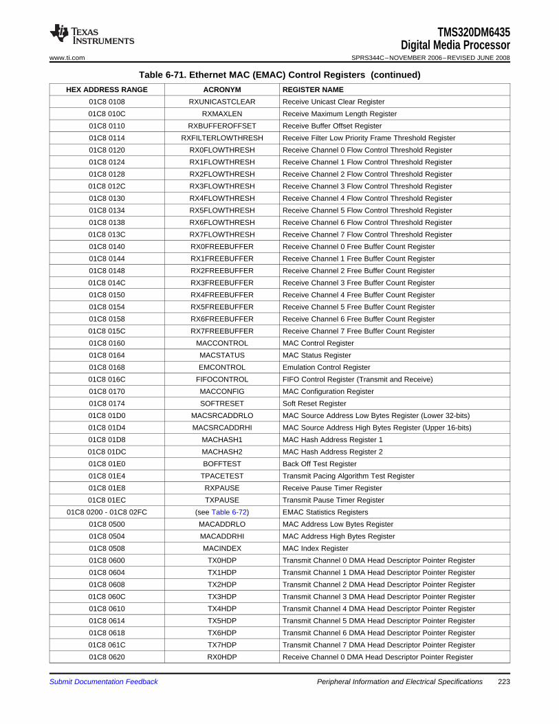
TMS320DM6435Digital Media Processor
www.ti.com SPRS344C–NOVEMBER 2006–REVISED JUNE 2008
Table 6-71. Ethernet MAC (EMAC) Control Registers (continued)HEX ADDRESS RANGE ACRONYM REGISTER NAME
01C8 0108 RXUNICASTCLEAR Receive Unicast Clear Register01C8 010C RXMAXLEN Receive Maximum Length Register01C8 0110 RXBUFFEROFFSET Receive Buffer Offset Register01C8 0114 RXFILTERLOWTHRESH Receive Filter Low Priority Frame Threshold Register01C8 0120 RX0FLOWTHRESH Receive Channel 0 Flow Control Threshold Register01C8 0124 RX1FLOWTHRESH Receive Channel 1 Flow Control Threshold Register01C8 0128 RX2FLOWTHRESH Receive Channel 2 Flow Control Threshold Register01C8 012C RX3FLOWTHRESH Receive Channel 3 Flow Control Threshold Register01C8 0130 RX4FLOWTHRESH Receive Channel 4 Flow Control Threshold Register01C8 0134 RX5FLOWTHRESH Receive Channel 5 Flow Control Threshold Register01C8 0138 RX6FLOWTHRESH Receive Channel 6 Flow Control Threshold Register01C8 013C RX7FLOWTHRESH Receive Channel 7 Flow Control Threshold Register01C8 0140 RX0FREEBUFFER Receive Channel 0 Free Buffer Count Register01C8 0144 RX1FREEBUFFER Receive Channel 1 Free Buffer Count Register01C8 0148 RX2FREEBUFFER Receive Channel 2 Free Buffer Count Register01C8 014C RX3FREEBUFFER Receive Channel 3 Free Buffer Count Register01C8 0150 RX4FREEBUFFER Receive Channel 4 Free Buffer Count Register01C8 0154 RX5FREEBUFFER Receive Channel 5 Free Buffer Count Register01C8 0158 RX6FREEBUFFER Receive Channel 6 Free Buffer Count Register01C8 015C RX7FREEBUFFER Receive Channel 7 Free Buffer Count Register01C8 0160 MACCONTROL MAC Control Register01C8 0164 MACSTATUS MAC Status Register01C8 0168 EMCONTROL Emulation Control Register01C8 016C FIFOCONTROL FIFO Control Register (Transmit and Receive)01C8 0170 MACCONFIG MAC Configuration Register01C8 0174 SOFTRESET Soft Reset Register01C8 01D0 MACSRCADDRLO MAC Source Address Low Bytes Register (Lower 32-bits)01C8 01D4 MACSRCADDRHI MAC Source Address High Bytes Register (Upper 16-bits)01C8 01D8 MACHASH1 MAC Hash Address Register 101C8 01DC MACHASH2 MAC Hash Address Register 201C8 01E0 BOFFTEST Back Off Test Register01C8 01E4 TPACETEST Transmit Pacing Algorithm Test Register01C8 01E8 RXPAUSE Receive Pause Timer Register01C8 01EC TXPAUSE Transmit Pause Timer Register
01C8 0200 - 01C8 02FC (see Table 6-72) EMAC Statistics Registers01C8 0500 MACADDRLO MAC Address Low Bytes Register01C8 0504 MACADDRHI MAC Address High Bytes Register01C8 0508 MACINDEX MAC Index Register01C8 0600 TX0HDP Transmit Channel 0 DMA Head Descriptor Pointer Register01C8 0604 TX1HDP Transmit Channel 1 DMA Head Descriptor Pointer Register01C8 0608 TX2HDP Transmit Channel 2 DMA Head Descriptor Pointer Register01C8 060C TX3HDP Transmit Channel 3 DMA Head Descriptor Pointer Register01C8 0610 TX4HDP Transmit Channel 4 DMA Head Descriptor Pointer Register01C8 0614 TX5HDP Transmit Channel 5 DMA Head Descriptor Pointer Register01C8 0618 TX6HDP Transmit Channel 6 DMA Head Descriptor Pointer Register01C8 061C TX7HDP Transmit Channel 7 DMA Head Descriptor Pointer Register01C8 0620 RX0HDP Receive Channel 0 DMA Head Descriptor Pointer Register
Submit Documentation Feedback Peripheral Information and Electrical Specifications 223
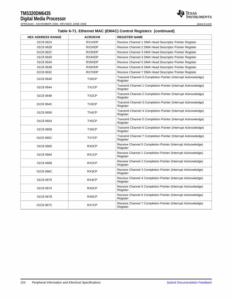
TMS320DM6435Digital Media ProcessorSPRS344C–NOVEMBER 2006–REVISED JUNE 2008 www.ti.com
Table 6-71. Ethernet MAC (EMAC) Control Registers (continued)HEX ADDRESS RANGE ACRONYM REGISTER NAME
01C8 0624 RX1HDP Receive Channel 1 DMA Head Descriptor Pointer Register01C8 0628 RX2HDP Receive Channel 2 DMA Head Descriptor Pointer Register01C8 062C RX3HDP Receive Channel 3 DMA Head Descriptor Pointer Register01C8 0630 RX4HDP Receive Channel 4 DMA Head Descriptor Pointer Register01C8 0634 RX5HDP Receive Channel 5 DMA Head Descriptor Pointer Register01C8 0638 RX6HDP Receive Channel 6 DMA Head Descriptor Pointer Register01C8 063C RX7HDP Receive Channel 7 DMA Head Descriptor Pointer Register
Transmit Channel 0 Completion Pointer (Interrupt Acknowledge)01C8 0640 TX0CP RegisterTransmit Channel 1 Completion Pointer (Interrupt Acknowledge)01C8 0644 TX1CP RegisterTransmit Channel 2 Completion Pointer (Interrupt Acknowledge)01C8 0648 TX2CP RegisterTransmit Channel 3 Completion Pointer (Interrupt Acknowledge)01C8 064C TX3CP RegisterTransmit Channel 4 Completion Pointer (Interrupt Acknowledge)01C8 0650 TX4CP RegisterTransmit Channel 5 Completion Pointer (Interrupt Acknowledge)01C8 0654 TX5CP RegisterTransmit Channel 6 Completion Pointer (Interrupt Acknowledge)01C8 0658 TX6CP RegisterTransmit Channel 7 Completion Pointer (Interrupt Acknowledge)01C8 065C TX7CP RegisterReceive Channel 0 Completion Pointer (Interrupt Acknowledge)01C8 0660 RX0CP RegisterReceive Channel 1 Completion Pointer (Interrupt Acknowledge)01C8 0664 RX1CP RegisterReceive Channel 2 Completion Pointer (Interrupt Acknowledge)01C8 0668 RX2CP RegisterReceive Channel 3 Completion Pointer (Interrupt Acknowledge)01C8 066C RX3CP RegisterReceive Channel 4 Completion Pointer (Interrupt Acknowledge)01C8 0670 RX4CP RegisterReceive Channel 5 Completion Pointer (Interrupt Acknowledge)01C8 0674 RX5CP RegisterReceive Channel 6 Completion Pointer (Interrupt Acknowledge)01C8 0678 RX6CP RegisterReceive Channel 7 Completion Pointer (Interrupt Acknowledge)01C8 067C RX7CP Register
224 Peripheral Information and Electrical Specifications Submit Documentation Feedback
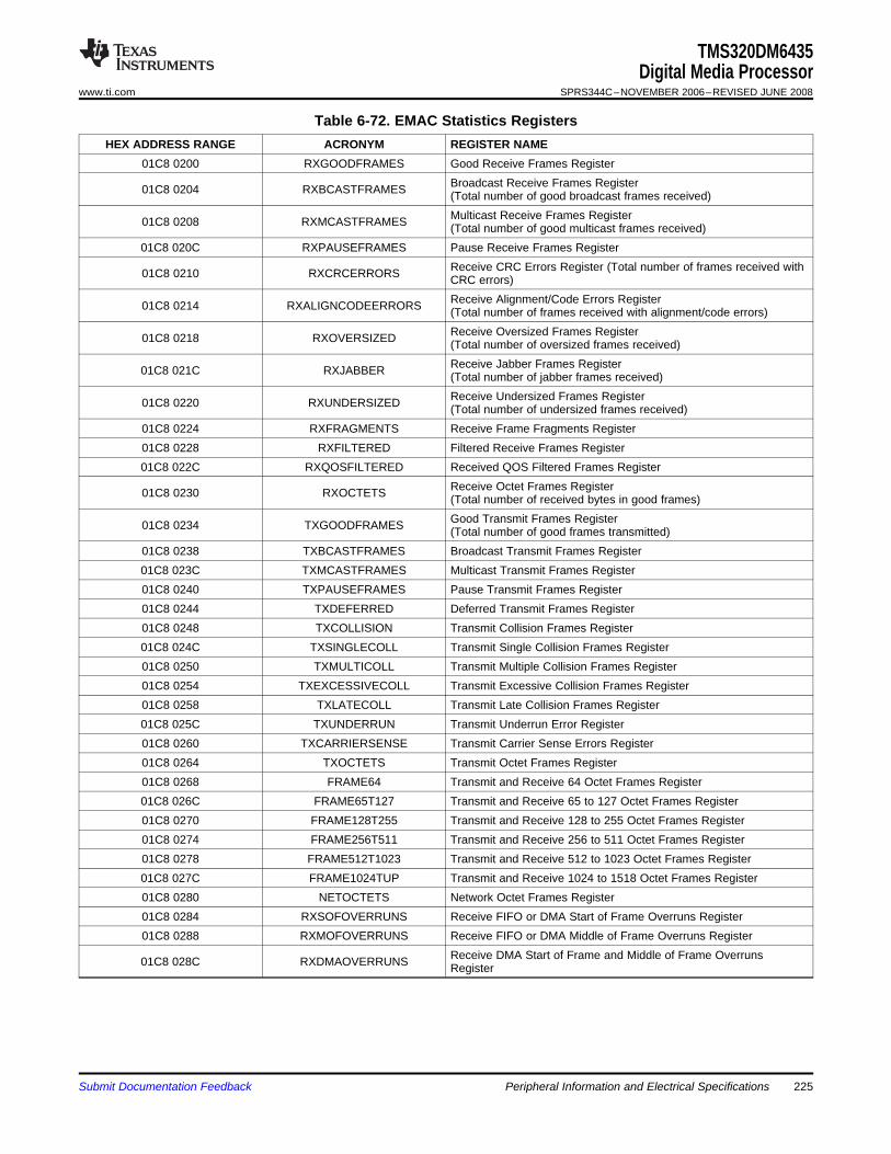
TMS320DM6435Digital Media Processor
www.ti.com SPRS344C–NOVEMBER 2006–REVISED JUNE 2008
Table 6-72. EMAC Statistics RegistersHEX ADDRESS RANGE ACRONYM REGISTER NAME
01C8 0200 RXGOODFRAMES Good Receive Frames RegisterBroadcast Receive Frames Register01C8 0204 RXBCASTFRAMES (Total number of good broadcast frames received)Multicast Receive Frames Register01C8 0208 RXMCASTFRAMES (Total number of good multicast frames received)
01C8 020C RXPAUSEFRAMES Pause Receive Frames RegisterReceive CRC Errors Register (Total number of frames received with01C8 0210 RXCRCERRORS CRC errors)Receive Alignment/Code Errors Register01C8 0214 RXALIGNCODEERRORS (Total number of frames received with alignment/code errors)Receive Oversized Frames Register01C8 0218 RXOVERSIZED (Total number of oversized frames received)Receive Jabber Frames Register01C8 021C RXJABBER (Total number of jabber frames received)Receive Undersized Frames Register01C8 0220 RXUNDERSIZED (Total number of undersized frames received)
01C8 0224 RXFRAGMENTS Receive Frame Fragments Register01C8 0228 RXFILTERED Filtered Receive Frames Register01C8 022C RXQOSFILTERED Received QOS Filtered Frames Register
Receive Octet Frames Register01C8 0230 RXOCTETS (Total number of received bytes in good frames)Good Transmit Frames Register01C8 0234 TXGOODFRAMES (Total number of good frames transmitted)
01C8 0238 TXBCASTFRAMES Broadcast Transmit Frames Register01C8 023C TXMCASTFRAMES Multicast Transmit Frames Register01C8 0240 TXPAUSEFRAMES Pause Transmit Frames Register01C8 0244 TXDEFERRED Deferred Transmit Frames Register01C8 0248 TXCOLLISION Transmit Collision Frames Register01C8 024C TXSINGLECOLL Transmit Single Collision Frames Register01C8 0250 TXMULTICOLL Transmit Multiple Collision Frames Register01C8 0254 TXEXCESSIVECOLL Transmit Excessive Collision Frames Register01C8 0258 TXLATECOLL Transmit Late Collision Frames Register01C8 025C TXUNDERRUN Transmit Underrun Error Register01C8 0260 TXCARRIERSENSE Transmit Carrier Sense Errors Register01C8 0264 TXOCTETS Transmit Octet Frames Register01C8 0268 FRAME64 Transmit and Receive 64 Octet Frames Register01C8 026C FRAME65T127 Transmit and Receive 65 to 127 Octet Frames Register01C8 0270 FRAME128T255 Transmit and Receive 128 to 255 Octet Frames Register01C8 0274 FRAME256T511 Transmit and Receive 256 to 511 Octet Frames Register01C8 0278 FRAME512T1023 Transmit and Receive 512 to 1023 Octet Frames Register01C8 027C FRAME1024TUP Transmit and Receive 1024 to 1518 Octet Frames Register01C8 0280 NETOCTETS Network Octet Frames Register01C8 0284 RXSOFOVERRUNS Receive FIFO or DMA Start of Frame Overruns Register01C8 0288 RXMOFOVERRUNS Receive FIFO or DMA Middle of Frame Overruns Register
Receive DMA Start of Frame and Middle of Frame Overruns01C8 028C RXDMAOVERRUNS Register
Submit Documentation Feedback Peripheral Information and Electrical Specifications 225
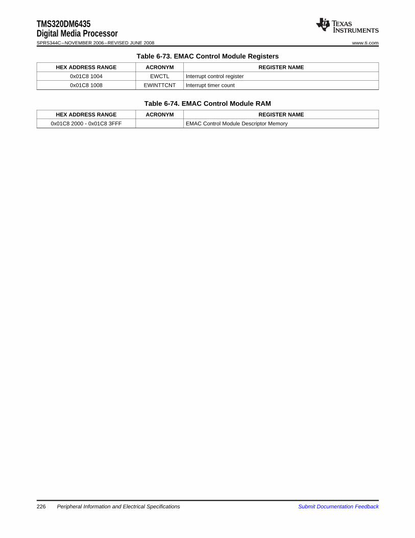
TMS320DM6435Digital Media ProcessorSPRS344C–NOVEMBER 2006–REVISED JUNE 2008 www.ti.com
Table 6-73. EMAC Control Module RegistersHEX ADDRESS RANGE ACRONYM REGISTER NAME
0x01C8 1004 EWCTL Interrupt control register0x01C8 1008 EWINTTCNT Interrupt timer count
Table 6-74. EMAC Control Module RAMHEX ADDRESS RANGE ACRONYM REGISTER NAME
0x01C8 2000 - 0x01C8 3FFF EMAC Control Module Descriptor Memory
Peripheral Information and Electrical Specifications226 Submit Documentation Feedback
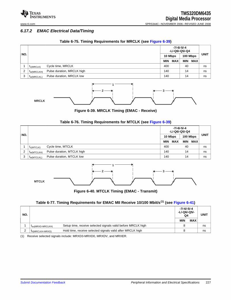
6.17.2 EMAC Electrical Data/Timing
MRCLK
2 3
1
MTCLK
2 3
1
TMS320DM6435Digital Media Processor
www.ti.com SPRS344C–NOVEMBER 2006–REVISED JUNE 2008
Table 6-75. Timing Requirements for MRCLK (see Figure 6-39)-7/-6/-5/-4
-L/-Q6/-Q5/-Q4NO. UNIT10 Mbps 100 Mbps
MIN MAX MIN MAX1 tc(MRCLK) Cycle time, MRCLK 400 40 ns2 tw(MRCLKH) Pulse duration, MRCLK high 140 14 ns3 tw(MRCLKL) Pulse duration, MRCLK low 140 14 ns
Figure 6-39. MRCLK Timing (EMAC - Receive)
Table 6-76. Timing Requirements for MTCLK (see Figure 6-39)-7/-6/-5/-4
-L/-Q6/-Q5/-Q4NO. UNIT10 Mbps 100 Mbps
MIN MAX MIN MAX1 tc(MTCLK) Cycle time, MTCLK 400 40 ns2 tw(MTCLKH) Pulse duration, MTCLK high 140 14 ns3 tw(MTCLKL) Pulse duration, MTCLK low 140 14 ns
Figure 6-40. MTCLK Timing (EMAC - Transmit)
Table 6-77. Timing Requirements for EMAC MII Receive 10/100 Mbit/s (1) (see Figure 6-41)-7/-6/-5/-4
-L/-Q6/-Q5/-NO. UNITQ4
MIN MAX1 tsu(MRXD-MRCLKH) Setup time, receive selected signals valid before MRCLK high 8 ns2 th(MRCLKH-MRXD) Hold time, receive selected signals valid after MRCLK high 8 ns
(1) Receive selected signals include: MRXD3-MRXD0, MRXDV, and MRXER.
Submit Documentation Feedback Peripheral Information and Electrical Specifications 227
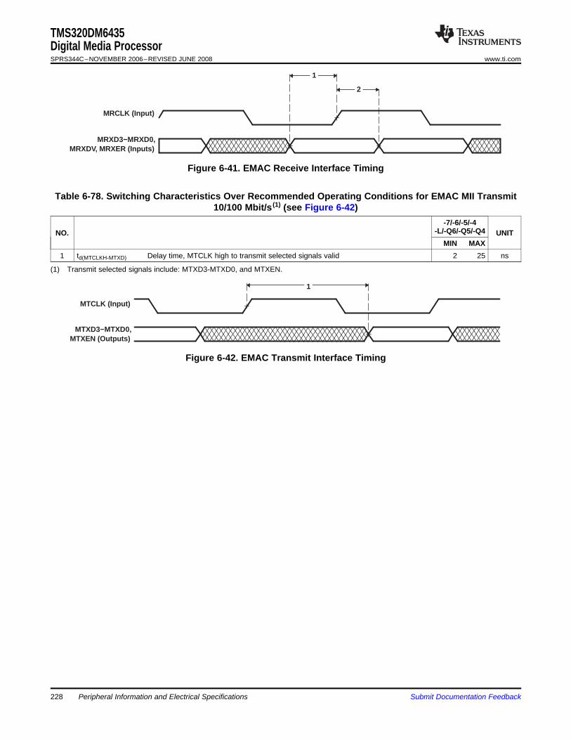
MRCLK (Input)
1
2
MRXD3−MRXD0,MRXDV, MRXER (Inputs)
1
MTCLK (Input)
MTXD3−MTXD0,MTXEN (Outputs)
TMS320DM6435Digital Media ProcessorSPRS344C–NOVEMBER 2006–REVISED JUNE 2008 www.ti.com
Figure 6-41. EMAC Receive Interface Timing
Table 6-78. Switching Characteristics Over Recommended Operating Conditions for EMAC MII Transmit10/100 Mbit/s (1) (see Figure 6-42)
-7/-6/-5/-4-L/-Q6/-Q5/-Q4NO. UNIT
MIN MAX1 td(MTCLKH-MTXD) Delay time, MTCLK high to transmit selected signals valid 2 25 ns
(1) Transmit selected signals include: MTXD3-MTXD0, and MTXEN.
Figure 6-42. EMAC Transmit Interface Timing
228 Peripheral Information and Electrical Specifications Submit Documentation Feedback
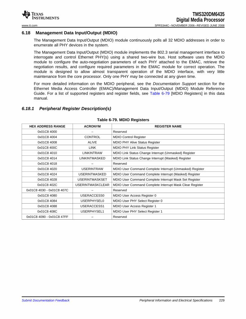
6.18 Management Data Input/Output (MDIO)
6.18.1 Peripheral Register Description(s)
TMS320DM6435Digital Media Processor
www.ti.com SPRS344C–NOVEMBER 2006–REVISED JUNE 2008
The Management Data Input/Output (MDIO) module continuously polls all 32 MDIO addresses in order toenumerate all PHY devices in the system.
The Management Data Input/Output (MDIO) module implements the 802.3 serial management interface tointerrogate and control Ethernet PHY(s) using a shared two-wire bus. Host software uses the MDIOmodule to configure the auto-negotiation parameters of each PHY attached to the EMAC, retrieve thenegotiation results, and configure required parameters in the EMAC module for correct operation. Themodule is designed to allow almost transparent operation of the MDIO interface, with very littlemaintenance from the core processor. Only one PHY may be connected at any given time.
For more detailed information on the MDIO peripheral, see the Documentation Support section for theEthernet Media Access Controller (EMAC)/Management Data Input/Output (MDIO) Module ReferenceGuide. For a list of supported registers and register fields, see Table 6-79 [MDIO Registers] in this datamanual.
Table 6-79. MDIO RegistersHEX ADDRESS RANGE ACRONYM REGISTER NAME
0x01C8 4000 – Reserved0x01C8 4004 CONTROL MDIO Control Register0x01C8 4008 ALIVE MDIO PHY Alive Status Register0x01C8 400C LINK MDIO PHY Link Status Register0x01C8 4010 LINKINTRAW MDIO Link Status Change Interrupt (Unmasked) Register0x01C8 4014 LINKINTMASKED MDIO Link Status Change Interrupt (Masked) Register0x01C8 4018 – Reserved0x01C8 4020 USERINTRAW MDIO User Command Complete Interrupt (Unmasked) Register0x01C8 4024 USERINTMASKED MDIO User Command Complete Interrupt (Masked) Register0x01C8 4028 USERINTMASKSET MDIO User Command Complete Interrupt Mask Set Register0x01C8 402C USERINTMASKCLEAR MDIO User Command Complete Interrupt Mask Clear Register
0x01C8 4030 - 0x01C8 407C – Reserved0x01C8 4080 USERACCESS0 MDIO User Access Register 00x01C8 4084 USERPHYSEL0 MDIO User PHY Select Register 00x01C8 4088 USERACCESS1 MDIO User Access Register 10x01C8 408C USERPHYSEL1 MDIO User PHY Select Register 1
0x01C8 4090 - 0x01C8 47FF – Reserved
Submit Documentation Feedback Peripheral Information and Electrical Specifications 229
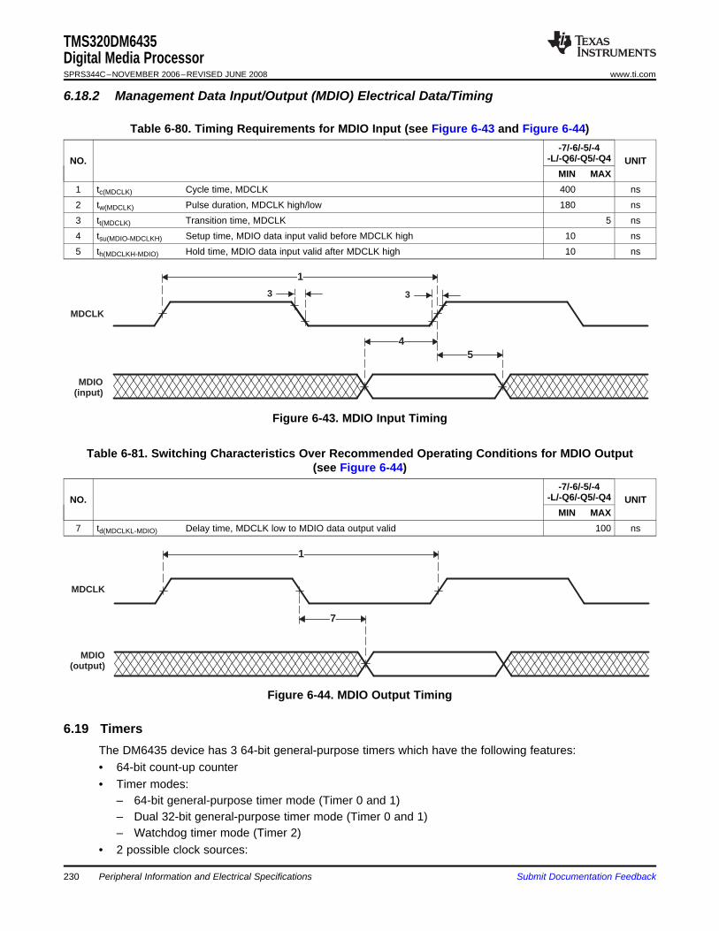
6.18.2 Management Data Input/Output (MDIO) Electrical Data/Timing
1
45
MDCLK
MDIO(input)
3 3
1
7
MDCLK
MDIO(output)
6.19 Timers
TMS320DM6435Digital Media ProcessorSPRS344C–NOVEMBER 2006–REVISED JUNE 2008 www.ti.com
Table 6-80. Timing Requirements for MDIO Input (see Figure 6-43 and Figure 6-44)-7/-6/-5/-4
-L/-Q6/-Q5/-Q4NO. UNITMIN MAX
1 tc(MDCLK) Cycle time, MDCLK 400 ns2 tw(MDCLK) Pulse duration, MDCLK high/low 180 ns3 tt(MDCLK) Transition time, MDCLK 5 ns4 tsu(MDIO-MDCLKH) Setup time, MDIO data input valid before MDCLK high 10 ns5 th(MDCLKH-MDIO) Hold time, MDIO data input valid after MDCLK high 10 ns
Figure 6-43. MDIO Input Timing
Table 6-81. Switching Characteristics Over Recommended Operating Conditions for MDIO Output(see Figure 6-44)
-7/-6/-5/-4-L/-Q6/-Q5/-Q4NO. UNIT
MIN MAX7 td(MDCLKL-MDIO) Delay time, MDCLK low to MDIO data output valid 100 ns
Figure 6-44. MDIO Output Timing
The DM6435 device has 3 64-bit general-purpose timers which have the following features:• 64-bit count-up counter• Timer modes:
– 64-bit general-purpose timer mode (Timer 0 and 1)– Dual 32-bit general-purpose timer mode (Timer 0 and 1)– Watchdog timer mode (Timer 2)
• 2 possible clock sources:
Peripheral Information and Electrical Specifications230 Submit Documentation Feedback
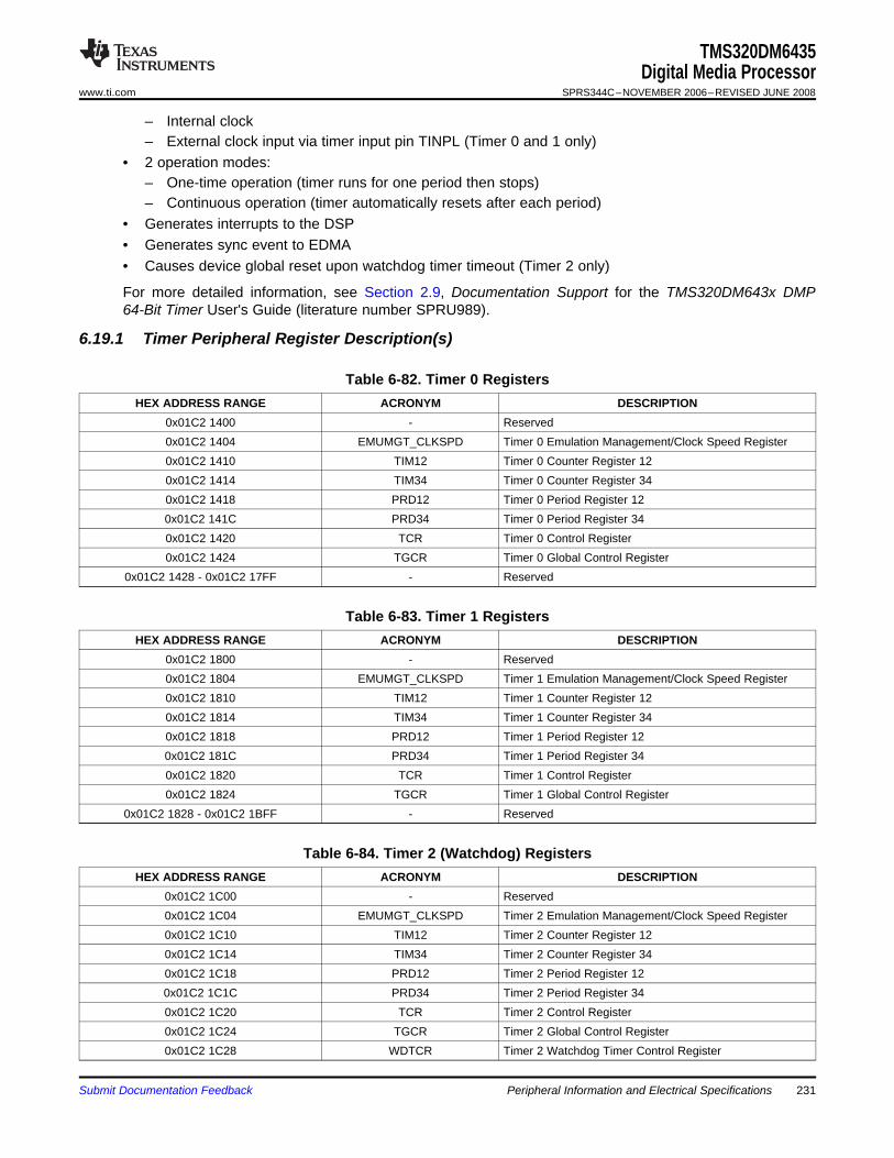
6.19.1 Timer Peripheral Register Description(s)
TMS320DM6435Digital Media Processor
www.ti.com SPRS344C–NOVEMBER 2006–REVISED JUNE 2008
– Internal clock– External clock input via timer input pin TINPL (Timer 0 and 1 only)
• 2 operation modes:– One-time operation (timer runs for one period then stops)– Continuous operation (timer automatically resets after each period)
• Generates interrupts to the DSP• Generates sync event to EDMA• Causes device global reset upon watchdog timer timeout (Timer 2 only)
For more detailed information, see Section 2.9, Documentation Support for the TMS320DM643x DMP64-Bit Timer User's Guide (literature number SPRU989).
Table 6-82. Timer 0 RegistersHEX ADDRESS RANGE ACRONYM DESCRIPTION
0x01C2 1400 - Reserved0x01C2 1404 EMUMGT_CLKSPD Timer 0 Emulation Management/Clock Speed Register0x01C2 1410 TIM12 Timer 0 Counter Register 120x01C2 1414 TIM34 Timer 0 Counter Register 340x01C2 1418 PRD12 Timer 0 Period Register 120x01C2 141C PRD34 Timer 0 Period Register 340x01C2 1420 TCR Timer 0 Control Register0x01C2 1424 TGCR Timer 0 Global Control Register
0x01C2 1428 - 0x01C2 17FF - Reserved
Table 6-83. Timer 1 RegistersHEX ADDRESS RANGE ACRONYM DESCRIPTION
0x01C2 1800 - Reserved0x01C2 1804 EMUMGT_CLKSPD Timer 1 Emulation Management/Clock Speed Register0x01C2 1810 TIM12 Timer 1 Counter Register 120x01C2 1814 TIM34 Timer 1 Counter Register 340x01C2 1818 PRD12 Timer 1 Period Register 120x01C2 181C PRD34 Timer 1 Period Register 340x01C2 1820 TCR Timer 1 Control Register0x01C2 1824 TGCR Timer 1 Global Control Register
0x01C2 1828 - 0x01C2 1BFF - Reserved
Table 6-84. Timer 2 (Watchdog) RegistersHEX ADDRESS RANGE ACRONYM DESCRIPTION
0x01C2 1C00 - Reserved0x01C2 1C04 EMUMGT_CLKSPD Timer 2 Emulation Management/Clock Speed Register0x01C2 1C10 TIM12 Timer 2 Counter Register 120x01C2 1C14 TIM34 Timer 2 Counter Register 340x01C2 1C18 PRD12 Timer 2 Period Register 120x01C2 1C1C PRD34 Timer 2 Period Register 340x01C2 1C20 TCR Timer 2 Control Register0x01C2 1C24 TGCR Timer 2 Global Control Register0x01C2 1C28 WDTCR Timer 2 Watchdog Timer Control Register
Submit Documentation Feedback Peripheral Information and Electrical Specifications 231
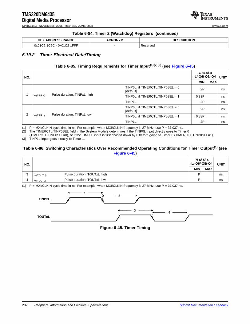
6.19.2 Timer Electrical Data/Timing
TINPxL
TOUTxL
12
34
TMS320DM6435Digital Media ProcessorSPRS344C–NOVEMBER 2006–REVISED JUNE 2008 www.ti.com
Table 6-84. Timer 2 (Watchdog) Registers (continued)HEX ADDRESS RANGE ACRONYM DESCRIPTION
0x01C2 1C2C - 0x01C2 1FFF - Reserved
Table 6-85. Timing Requirements for Timer Input (1) (2) (3) (see Figure 6-45)-7/-6/-5/-4
-L/-Q6/-Q5/-Q4NO. UNITMIN MAX
TINP0L, if TIMERCTL.TINP0SEL = 0 2P ns[default]1 tw(TINPH) Pulse duration, TINPxL high TINP0L, if TIMERCTL.TINP0SEL = 1 0.33P ns
TINP1L 2P nsTINP0L, if TIMERCTL.TINP0SEL = 0 2P ns[default]
2 tw(TINPL) Pulse duration, TINPxL low TINP0L, if TIMERCTL.TINP0SEL = 1 0.33P nsTINP1L 2P ns
(1) P = MXI/CLKIN cycle time in ns. For example, when MXI/CLKIN frequency is 27 MHz, use P = 37.037 ns.(2) The TIMERCTL.TINP0SEL field in the System Module determines if the TINP0L input directly goes to Timer 0
(TIMERCTL.TINP0SEL=0), or if the TINP0L input is first divided down by 6 before going to Timer 0 (TIMERCTL.TINP0SEL=1).(3) TINP1L input goes directly to Timer 1.
Table 6-86. Switching Characteristics Over Recommended Operating Conditions for Timer Output (1) (seeFigure 6-45)
-7/-6/-5/-4-L/-Q6/-Q5/-Q4NO. UNIT
MIN MAX3 tw(TOUTH) Pulse duration, TOUTxL high P ns4 tw(TOUTL) Pulse duration, TOUTxL low P ns
(1) P = MXI/CLKIN cycle time in ns. For example, when MXI/CLKIN frequency is 27 MHz, use P = 37.037 ns.
Figure 6-45. Timer Timing
232 Peripheral Information and Electrical Specifications Submit Documentation Feedback
6.20 Pulse Width Modulator (PWM)
TMS320DM6435Digital Media Processor
www.ti.com SPRS344C–NOVEMBER 2006–REVISED JUNE 2008
The 3 DM6435 Pulse Width Modulator (PWM) peripherals support the following features:• Period counter• First-phase duration counter• Repeat count for one-shot operation• Configurable to operate in either one-shot or continuous mode• Buffered period and first-phase duration registers• One-shot operation triggerable by hardware events with programmable edge transitions. (low-to-high or
high-to-low).• One-shot operation generates N+1 periods of waveform, N being the repeat count register value• Emulation support
The register memory maps for PWM0/1/2 are shown in Table 6-87, Table 6-88, and Table 6-89.
Table 6-87. PWM0 Register Memory MapHEX ADDRESS RANGE ACRONYM REGISTER NAME
0x01C2 2000 Reserved0x01C2 2004 PCR PWM0 Peripheral Control Register0x01C2 2008 CFG PWM0 Configuration Register0x01C2 200C START PWM0 Start Register0x01C2 2010 RPT PWM0 Repeat Count Register0x01C2 2014 PER PWM0 Period Register0x01C2 2018 PH1D PWM0 First-Phase Duration Register0x01C2 201C - 0x01C2 23FF - Reserved
Table 6-88. PWM1 Register Memory MapHEX ADDRESS RANGE ACRONYM REGISTER NAME
0x01C2 2400 Reserved0x01C2 2404 PCR PWM1 Peripheral Control Register0x01C2 2408 CFG PWM1 Configuration Register0x01C2 240C START PWM1 Start Register0x01C2 2410 RPT PWM1 Repeat Count Register0x01C2 2414 PER PWM1 Period Register0x01C2 2418 PH1D PWM1 First-Phase Duration Register0x01C2 241C -0x01C2 27FF - Reserved
Table 6-89. PWM2 Register Memory MapHEX ADDRESS RANGE ACRONYM REGISTER NAME
0x01C2 2800 Reserved0x01C2 2804 PCR PWM2 Peripheral Control Register0x01C2 2808 CFG PWM2 Configuration Register0x01C2 280C START PWM2 Start Register0x01C2 2810 RPT PWM2 Repeat Count Register0x01C2 2814 PER PWM2 Period Register0x01C2 2818 PH1D PWM2 First-Phase Duration Register0x01C2 281C - 0x01C2 2BFF - Reserved
Submit Documentation Feedback Peripheral Information and Electrical Specifications 233
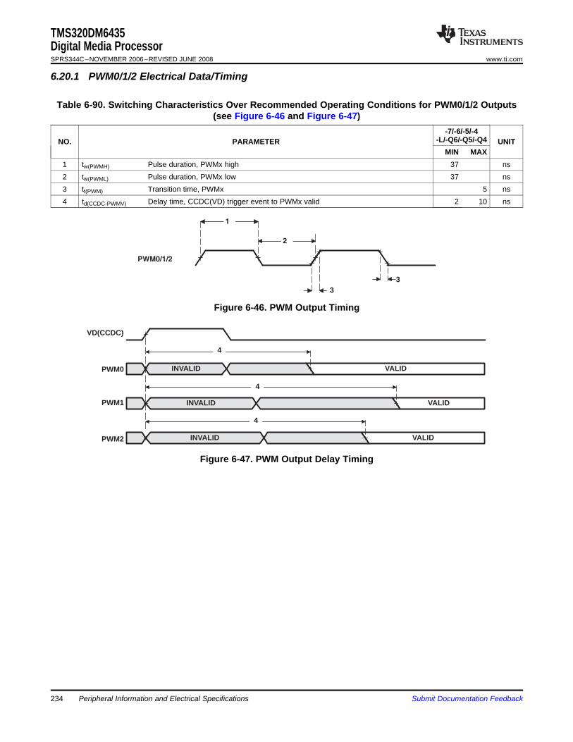
6.20.1 PWM0/1/2 Electrical Data/Timing
PWM0/1/2
1
3
3
2
4
VD(CCDC)
4
4
INVALID
INVALID
INVALID
VALID
VALID
VALID
PWM0
PWM1
PWM2
TMS320DM6435Digital Media ProcessorSPRS344C–NOVEMBER 2006–REVISED JUNE 2008 www.ti.com
Table 6-90. Switching Characteristics Over Recommended Operating Conditions for PWM0/1/2 Outputs(see Figure 6-46 and Figure 6-47)
-7/-6/-5/-4-L/-Q6/-Q5/-Q4NO. PARAMETER UNIT
MIN MAX1 tw(PWMH) Pulse duration, PWMx high 37 ns2 tw(PWML) Pulse duration, PWMx low 37 ns3 tt(PWM) Transition time, PWMx 5 ns4 td(CCDC-PWMV) Delay time, CCDC(VD) trigger event to PWMx valid 2 10 ns
Figure 6-46. PWM Output Timing
Figure 6-47. PWM Output Delay Timing
234 Peripheral Information and Electrical Specifications Submit Documentation Feedback
6.21 VLYNQ
6.21.1 VLYNQ Peripheral Register Description(s)
TMS320DM6435Digital Media Processor
www.ti.com SPRS344C–NOVEMBER 2006–REVISED JUNE 2008
The DM6435 VLYNQ peripheral provides a high speed serial communications interface with the followingfeatures.• Low Pin Count• Scalable Performance / Support• Simple Packet Based Transfer Protocol for Memory Mapped Access
– Write Request / Data Packet– Read Request Packet– Read Response Data Packet– Interrupt Request Packet
• Supports both Symmetric and Asymmetric Operation– Tx pins on first device connect to Rx pins on second device and vice versa– Data pin widths are automatically detected after reset– Request packets, response packets, and flow control information are all multiplexed and sent
across the same physical pins– Supports both Host/Peripheral and Peer to Peer communication
• Simple Block Code Packet Formatting (8b/10b)• In Band Flow Control
– No extra pins needed– Allows receiver to momentarily throttle back transmitter when overflow is about to occur– Uses built in special code capability of block code to seamlessly interleave flow control information
with user data– Allows system designer to balance cost of data buffering versus performance
• Multiple outstanding transactions• Automatic packet formatting optimizations• Internal loop-back mode
Table 6-91. VLYNQ RegistersHEX ADDRESS RANGE ACRONYM REGISTER NAME
0x01E0 1000 - Reserved0x01E0 1004 CTRL VLYNQ Local Control Register0x01E0 1008 STAT VLYNQ Local Status Register0x01E0 100C INTPRI VLYNQ Local Interrupt Priority Vector Status/Clear Register0x01E0 1010 INTSTATCLR VLYNQ Local Unmasked Interrupt Status/Clear Register0x01E0 1014 INTPENDSET VLYNQ Local Interrupt Pending/Set Register0x01E0 1018 INTPTR VLYNQ Local Interrupt Pointer Register0x01E0 101C XAM VLYNQ Local Transmit Address Map Register0x01E0 1020 RAMS1 VLYNQ Local Receive Address Map Size 1 Register0x01E0 1024 RAMO1 VLYNQ Local Receive Address Map Offset 1 Register0x01E0 1028 RAMS2 VLYNQ Local Receive Address Map Size 2 Register0x01E0 102C RAMO2 VLYNQ Local Receive Address Map Offset 2 Register0x01E0 1030 RAMS3 VLYNQ Local Receive Address Map Size 3 Register0x01E0 1034 RAMO3 VLYNQ Local Receive Address Map Offset 3 Register0x01E0 1038 RAMS4 VLYNQ Local Receive Address Map Size 4 Register0x01E0 103C RAMO4 VLYNQ Local Receive Address Map Offset 4 Register
Submit Documentation Feedback Peripheral Information and Electrical Specifications 235
TMS320DM6435Digital Media ProcessorSPRS344C–NOVEMBER 2006–REVISED JUNE 2008 www.ti.com
Table 6-91. VLYNQ Registers (continued)HEX ADDRESS RANGE ACRONYM REGISTER NAME
0x01E0 1040 CHIPVER VLYNQ Local Chip Version Register0x01E0 1044 AUTNGO VLYNQ Local Auto Negotiation Register0x01E0 1048 - Reserved0x01E0 104C - Reserved
0x01E0 1050 - 0x01E0 105C - Reserved0x01E0 1060 - Reserved
01E0 10C00 0064 - Reserved0x01E0 1068 - 0x01E0 107C - Reserved for future use
0x01E0 1080 RREVID VLYNQ Remote Revision Register0x01E0 1084 RCTRL VLYNQ Remote Control Register0x01E0 1088 RSTAT VLYNQ Remote Status Register0x01E0 108C RINTPRI VLYNQ Remote Interrupt Priority Vector Status/Clear Register0x01E0 1090 RINTSTATCLR VLYNQ Remote Unmasked Interrupt Status/Clear Register0x01E0 1094 RINTPENDSET VLYNQ Remote Interrupt Pending/Set Register0x01E0 1098 RINTPTR VLYNQ Remote Interrupt Pointer Register0x01E0 109C RXAM VLYNQ Remote Transmit Address Map Register0x01E0 10A0 RRAMS1 VLYNQ Remote Receive Address Map Size 1 Register0x01E0 10A4 RRAMO1 VLYNQ Remote Receive Address Map Offset 1 Register0x01E0 10A8 RRAMS2 VLYNQ Remote Receive Address Map Size 2 Register0x01E0 10AC RRAMO2 VLYNQ Remote Receive Address Map Offset 2 Register0x01E0 10B0 RRAMS3 VLYNQ Remote Receive Address Map Size 3 Register0x01E0 10B4 RRAMO3 VLYNQ Remote Receive Address Map Offset 3 Register0x01E0 10B8 RRAMS4 VLYNQ Remote Receive Address Map Size 4 Register0x01E0 10BC RRAMO4 VLYNQ Remote Receive Address Map Offset 4 Register
VLYNQ Remote Chip Version Register (values on the device_id and0x01E0 10C0 RCHIPVER device_rev pins of remote VLYNQ)0x01E0 10C4 RAUTNGO VLYNQ Remote Auto Negotiation Register0x01E0 10C8 RMANNGO VLYNQ Remote Manual Negotiation Register0x01E0 10CC RNGOSTAT VLYNQ Remote Negotiation Status Register
0x01E0 10D0 - 0x01E0 10DC - ReservedVLYNQ Remote Interrupt Vectors 3 - 0 (sourced from vlynq_int_i[3:0] port of0x01E0 10E0 RINTVEC0 remote VLYNQ)VLYNQ Remote Interrupt Vectors 7 - 4 (sourced from vlynq_int_i[7:4] port of0x01E0 10E4 RINTVEC1 remote VLYNQ)
0x01E0 10E8 - 0x01E0 10FC - Reserved for future use0x01E0 1100 - 0x01E0 1FFF - Reserved
Peripheral Information and Electrical Specifications236 Submit Documentation Feedback
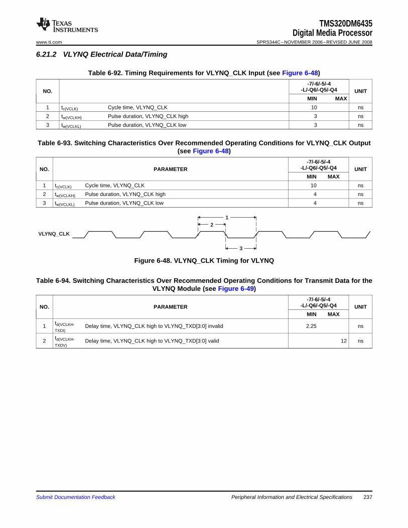
6.21.2 VLYNQ Electrical Data/Timing
VLYNQ_CLK
3
12
TMS320DM6435Digital Media Processor
www.ti.com SPRS344C–NOVEMBER 2006–REVISED JUNE 2008
Table 6-92. Timing Requirements for VLYNQ_CLK Input (see Figure 6-48)-7/-6/-5/-4
-L/-Q6/-Q5/-Q4NO. UNITMIN MAX
1 tc(VCLK) Cycle time, VLYNQ_CLK 10 ns2 tw(VCLKH) Pulse duration, VLYNQ_CLK high 3 ns3 tw(VCLKL) Pulse duration, VLYNQ_CLK low 3 ns
Table 6-93. Switching Characteristics Over Recommended Operating Conditions for VLYNQ_CLK Output(see Figure 6-48)
-7/-6/-5/-4-L/-Q6/-Q5/-Q4NO. PARAMETER UNIT
MIN MAX1 tc(VCLK) Cycle time, VLYNQ_CLK 10 ns2 tw(VCLKH) Pulse duration, VLYNQ_CLK high 4 ns3 tw(VCLKL) Pulse duration, VLYNQ_CLK low 4 ns
Figure 6-48. VLYNQ_CLK Timing for VLYNQ
Table 6-94. Switching Characteristics Over Recommended Operating Conditions for Transmit Data for theVLYNQ Module (see Figure 6-49)
-7/-6/-5/-4-L/-Q6/-Q5/-Q4NO. PARAMETER UNIT
MIN MAXtd(VCLKH-1 Delay time, VLYNQ_CLK high to VLYNQ_TXD[3:0] invalid 2.25 nsTXDI)
td(VCLKH-2 Delay time, VLYNQ_CLK high to VLYNQ_TXD[3:0] valid 12 nsTXDV)
Submit Documentation Feedback Peripheral Information and Electrical Specifications 237
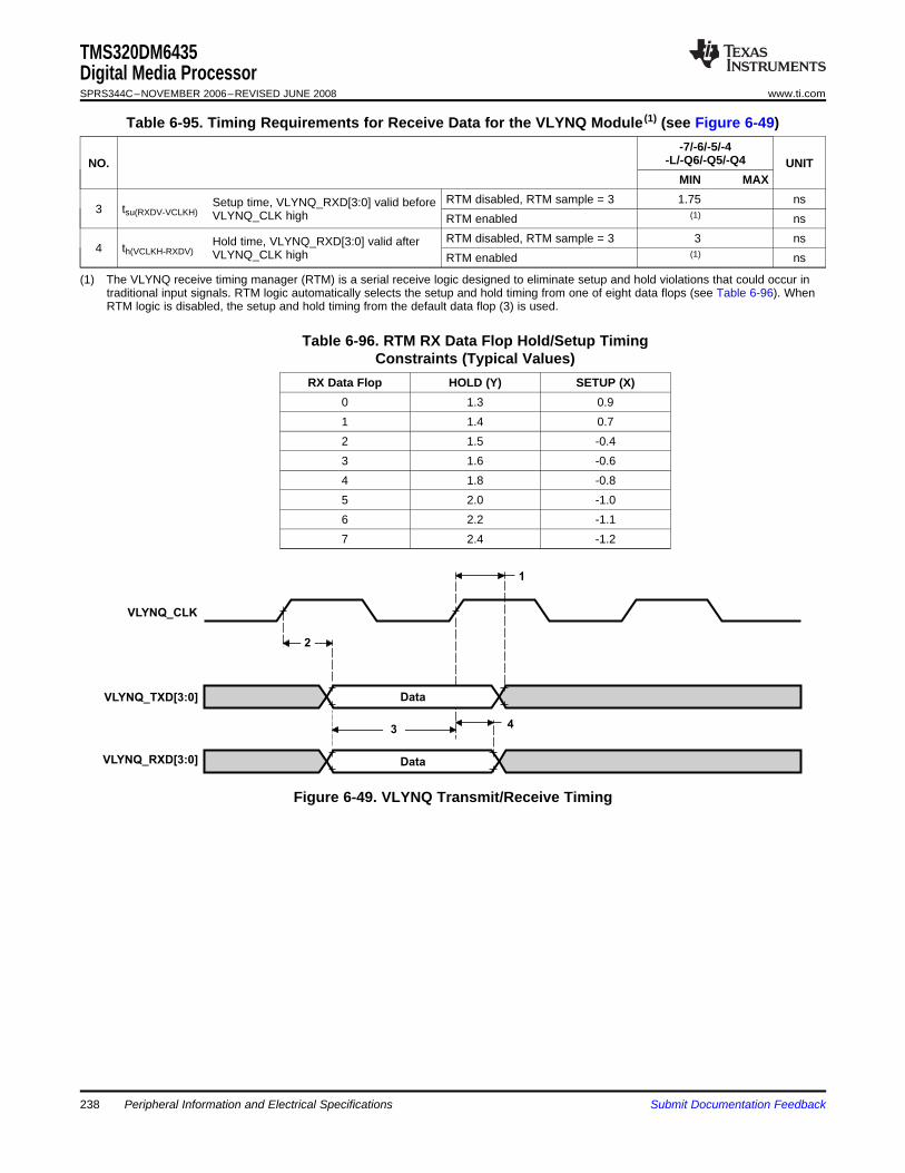
VLYNQ_CLK
VLYNQ_TXD[3:0]
VLYNQ_RXD[3:0]
1
2
3 4
Data
Data
TMS320DM6435Digital Media ProcessorSPRS344C–NOVEMBER 2006–REVISED JUNE 2008 www.ti.com
Table 6-95. Timing Requirements for Receive Data for the VLYNQ Module (1) (see Figure 6-49)-7/-6/-5/-4
-L/-Q6/-Q5/-Q4NO. UNITMIN MAX
RTM disabled, RTM sample = 3 1.75 nsSetup time, VLYNQ_RXD[3:0] valid before3 tsu(RXDV-VCLKH) VLYNQ_CLK high RTM enabled (1) nsRTM disabled, RTM sample = 3 3 nsHold time, VLYNQ_RXD[3:0] valid after4 th(VCLKH-RXDV) VLYNQ_CLK high RTM enabled (1) ns
(1) The VLYNQ receive timing manager (RTM) is a serial receive logic designed to eliminate setup and hold violations that could occur intraditional input signals. RTM logic automatically selects the setup and hold timing from one of eight data flops (see Table 6-96). WhenRTM logic is disabled, the setup and hold timing from the default data flop (3) is used.
Table 6-96. RTM RX Data Flop Hold/Setup TimingConstraints (Typical Values)
RX Data Flop HOLD (Y) SETUP (X)0 1.3 0.91 1.4 0.72 1.5 -0.43 1.6 -0.64 1.8 -0.85 2.0 -1.06 2.2 -1.17 2.4 -1.2
Figure 6-49. VLYNQ Transmit/Receive Timing
238 Peripheral Information and Electrical Specifications Submit Documentation Feedback
6.22 General-Purpose Input/Output (GPIO)
TMS320DM6435Digital Media Processor
www.ti.com SPRS344C–NOVEMBER 2006–REVISED JUNE 2008
The GPIO peripheral provides general-purpose pins that can be configured as either inputs or outputs.When configured as an output, a write to an internal register can control the state driven on the output pin.When configured as an input, the state of the input is detectable by reading the state of an internalregister. In addition, the GPIO peripheral can produce CPU interrupts and EDMA events in differentinterrupt/event generation modes. The GPIO peripheral provides generic connections to external devices.The GPIO pins are grouped into banks of 16 pins per bank (i.e., bank 0 consists of GP[0:15]).
The DM6435 GPIO peripheral supports the following:• Up to 111 3.3-V GPIO pins, GP[0:110]• Interrupts:
– Up to 8 unique GP[0:7] interrupts from Bank 0– 7 GPIO bank (aggregated) interrupt signals from each of the 7 banks of GPIOs– Interrupts can be triggered by rising and/or falling edge, specified for each interrupt capable GPIO
signal• DMA events:
– Up to 8 unique GPIO DMA events from Bank 0– 7 GPIO bank (aggregated) DMA event signals from each of the 7 banks of GPIOs
• Set/clear functionality: Firmware writes 1 to corresponding bit position(s) to set or to clear GPIOsignal(s). This allows multiple firmware processes to toggle GPIO output signals without critical sectionprotection (disable interrupts, program GPIO, re-enable interrupts, to prevent context switching toanther process during GPIO programming).
• Separate Input/Output registers• Output register in addition to set/clear so that, if preferred by firmware, some GPIO output signals can
be toggled by direct write to the output register(s).• Output register, when read, reflects output drive status. This, in addition to the input register reflecting
pin status and open-drain I/O cell, allows wired logic be implemented.
The memory map for the GPIO registers is shown in Table 6-97. For more detailed information on GPIOs,see the TMS320DM643x DMP General-Purpose Input/Output (GPIO) User's Guide (literature numberSPRU988).
Submit Documentation Feedback Peripheral Information and Electrical Specifications 239
6.22.1 GPIO Peripheral Register Description(s)
TMS320DM6435Digital Media ProcessorSPRS344C–NOVEMBER 2006–REVISED JUNE 2008 www.ti.com
Table 6-97. GPIO RegistersHEX ADDRESS RANGE ACRONYM REGISTER NAME
0x01C6 7000 PID Peripheral Identification Register0x01C6 7004 - Reserved0x01C6 7008 BINTEN GPIO interrupt per-bank enable
GPIO Banks 0 and 10x01C6 700C - Reserved0x01C6 7010 DIR01 GPIO Banks 0 and 1 Direction Register (GP[0:31])0x01C6 7014 OUT_DATA01 GPIO Banks 0 and 1 Output Data Register (GP[0:31])0x01C6 7018 SET_DATA01 GPIO Banks 0 and 1 Set Data Register (GP[0:31])0x01C6 701C CLR_DATA01 GPIO Banks 0 and 1 Clear data for banks 0 and 1 (GP[0:31])0x01C6 7020 IN_DATA01 GPIO Banks 0 and 1 Input Data Register (GP[0:31])0x01C6 7024 SET_RIS_TRIG01 GPIO Banks 0 and 1 Set Rising Edge Interrupt Register (GP[0:31])0x01C6 7028 CLR_RIS_TRIG01 GPIO Banks 0 and 1 Clear Rising Edge Interrupt Register (GP[0:31])0x01C6 702C SET_FAL_TRIG01 GPIO Banks 0 and 1 Set Falling Edge Interrupt Register (GP[0:31])0x01C6 7030 CLR_FAL_TRIG01 GPIO Banks 0 and 1 Clear Falling Edge Interrupt Register (GP[0:31])0x01C6 7034 INSTAT01 GPIO Banks 0 and 1 Interrupt Status Register (GP[0:31])
GPIO Banks 2 and 30x01C6 7038 DIR23 GPIO Banks 2 and 3 Direction Register (GP[32:63])0x01C6 703C OUT_DATA23 GPIO Banks 2 and 3 Output Data Register (GP[32:63])0x01C6 7040 SET_DATA23 GPIO Banks 2 and 3 Set Data Register (GP[32:63])0x01C6 7044 CLR_DATA23 GPIO Banks 2 and 3 Clear Data Register (GP[32:63])0x01C6 7048 IN_DATA23 GPIO Banks 2 and 3 Input Data Register (GP[32:63])0x01C6 704C SET_RIS_TRIG23 GPIO Banks 2 and 3 Set Rising Edge Interrupt Register (GP[32:63])0x01C6 7050 CLR_RIS_TRIG23 GPIO Banks 2 and 3 Clear Rising Edge Interrupt Register (GP[32:63])0x01C6 7054 SET_FAL_TRIG23 GPIO Banks 2 and 3 Set Falling Edge Interrupt Register (GP[32:63])0x01C6 7058 CLR_FAL_TRIG23 GPIO Banks 2 and 3 Clear Falling Edge Interrupt Register (GP[32:63])0x01C6 705C INSTAT23 GPIO Banks 2 and 3 Interrupt Status Register (GP[32:63])
GPIO Bank 4 and 50x01C6 7060 DIR45 GPIO Bank 4 and 5 Direction Register (GP[64:95])0x01C6 7064 OUT_DATA45 GPIO Bank 4 and 5 Output Data Register (GP[64:95])0x01C6 7068 SET_DATA45 GPIO Bank 4 and 5 Set Data Register (GP[64:95])0x01C6 706C CLR_DATA45 GPIO Bank 4 and 5 Clear Data Register (GP[64:95])0x01C6 7070 IN_DATA45 GPIO Bank 4 and 5 Input Data Register (GP[64:95])0x01C6 7074 SET_RIS_TRIG45 GPIO Bank 4 and 5 Set Rising Edge Interrupt Register (GP[64:95])0x01C6 7078 CLR_RIS_TRIG45 GPIO Bank 4 and 5 Clear Rising Edge Interrupt Register (GP[64:95])0x01C6 707C SET_FAL_TRIG45 GPIO Bank 4 and 5 Set Falling Edge Interrupt Register (GP[64:95])0x01C6 7080 CLR_FAL_TRIG45 GPIO Bank 4 and 5 Clear Falling Edge Interrupt Register (GP[64:95])0x01C6 7084 INSTAT45 GPIO Bank 4 and 5 Interrupt Status Register (GP[64:95])
GPIO Bank 60x01C6 7088 DIR6 GPIO Bank 6 Direction Register (GP[96:110])0x01C6 708C OUT_DATA6 GPIO Bank 6 Output Data Register (GP[96:110])0x01C6 7090 SET_DATA6 GPIO Bank 6 Set Data Register (GP[96:110])0x01C6 7094 CLR_DATA6 GPIO Bank 6 Clear Data Register (GP[96:110])0x01C6 7098 IN_DATA6 GPIO Bank 6 Input Data Register (GP[96:110])0x01C6 709C SET_RIS_TRIG6 GPIO Bank 6 Set Rising Edge Interrupt Register (GP[96:110])0x01C6 70A0 CLR_RIS_TRIG6 GPIO Bank 6 Clear Rising Edge Interrupt Register (GP[96:110])
Peripheral Information and Electrical Specifications240 Submit Documentation Feedback
TMS320DM6435Digital Media Processor
www.ti.com SPRS344C–NOVEMBER 2006–REVISED JUNE 2008
Table 6-97. GPIO Registers (continued)HEX ADDRESS RANGE ACRONYM REGISTER NAME
0x01C6 70A4 SET_FAL_TRIG6 GPIO Bank 6 Set Falling Edge Interrupt Register (GP[96:110])0x01C6 70A8 CLR_FAL_TRIG6 GPIO Bank 6 Clear Falling Edge Interrupt Register (GP[96:110])0x01C6 70AC INSTAT6 GPIO Bank 6 Interrupt Status Register (GP[96:110])
0x01C6 70B0 - 0x01C6 7FFF - Reserved
Submit Documentation Feedback Peripheral Information and Electrical Specifications 241
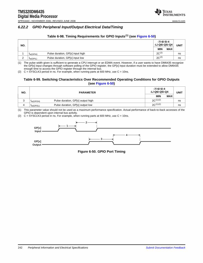
6.22.2 GPIO Peripheral Input/Output Electrical Data/Timing
GP[x]Input
GP[x]Output
4
3
21
TMS320DM6435Digital Media ProcessorSPRS344C–NOVEMBER 2006–REVISED JUNE 2008 www.ti.com
Table 6-98. Timing Requirements for GPIO Inputs (1) (see Figure 6-50)-7/-6/-5/-4
-L/-Q6/-Q5/-Q4NO. UNITMIN MAX
1 tw(GPIH) Pulse duration, GP[x] input high 2C (2) ns2 tw(GPIL) Pulse duration, GP[x] input low 2C (2) ns
(1) The pulse width given is sufficient to generate a CPU interrupt or an EDMA event. However, if a user wants to have DM6435 recognizethe GP[x] input changes through software polling of the GPIO register, the GP[x] input duration must be extended to allow DM6435enough time to access the GPIO register through the internal bus.
(2) C = SYSCLK3 period in ns. For example, when running parts at 600 MHz, use C = 10ns.
Table 6-99. Switching Characteristics Over Recommended Operating Conditions for GPIO Outputs(see Figure 6-50)
-7/-6/-5/-4-L/-Q6/-Q5/-Q4NO. PARAMETER UNIT
MIN MAX3 tw(GPOH) Pulse duration, GP[x] output high 2C (1) (2) ns4 tw(GPOL) Pulse duration, GP[x] output low 2C (1) (2) ns
(1) This parameter value should not be used as a maximum performance specification. Actual performance of back-to-back accesses of theGPIO is dependent upon internal bus activity.
(2) C = SYSCLK3 period in ns. For example, when running parts at 600 MHz, use C = 10ns.
Figure 6-50. GPIO Port Timing
242 Peripheral Information and Electrical Specifications Submit Documentation Feedback
6.23 IEEE 1149.1 JTAG
6.23.1 JTAG ID (JTAGID) Register Description(s)
TMS320DM6435Digital Media Processor
www.ti.com SPRS344C–NOVEMBER 2006–REVISED JUNE 2008
The JTAG (3) interface is used for BSDL testing and emulation of the DM6435 device.
TRST only needs to be released when it is necessary to use a JTAG controller to debug the device orexercise the device's boundary scan functionality. Note: TRST is synchronous and must be clocked byTCK; otherwise, the boundary scan logic may not respond as expected after TRST is asserted.
For maximum reliability, DM6435 includes an internal pulldown (IPD) on the TRST pin to ensure thatTRST will always be asserted upon power up and the device's internal emulation logic will always beproperly initialized.
JTAG controllers from Texas Instruments actively drive TRST high. However, some third-party JTAGcontrollers may not drive TRST high but expect the use of a pullup resistor on TRST.
When using this type of JTAG controller, assert TRST to initialize the device after powerup and externallydrive TRST high before attempting any emulation or boundary scan operations.
(3) IEEE Standard 1149.1-1990 Standard-Test-Access Port and Boundary Scan Architecture.
Table 6-100. JTAG ID (JTAGID) RegisterHEX ADDRESS RANGE ACRONYM REGISTER NAME COMMENTS
Read-only. Provides 32-bit0x01C4 0028 JTAGID JTAG Identification Register JTAG ID of the device.
The JTAG ID register is a read-only register that identifies to the customer the JTAG/Device ID. For theDM6435 device, the JTAG ID register resides at address location 0x01C4 0028. For the actual register bitnames and their associated bit field descriptions, see Figure 6-51 and Table 6-101.
31-28 27-12 11-1 0
VARIANT (4-Bit) PART NUMBER (16-Bit) MANUFACTURER (11-Bit) LSB
R-n R-1011 0111 0010 0001 R-0000 0010 111 R-1
LEGEND: R = Read, W = Write, n = value at reset
Figure 6-51. JTAG ID (JTAGID) Register—0x01C4 0028
Table 6-101. JTAG ID (JTAGID) Register Selection Bit DescriptionsBIT NAME DESCRIPTION
31:28 VARIANT Variant (4-Bit) value. A read from this field always returns 0b0000.27:12 PART NUMBER Part Number (16-Bit) value. DM6435 value: 1011 0111 0010 0001.11-1 MANUFACTURER Manufacturer (11-Bit) value. DM6435 value: 0000 0010 111.
0 LSB LSB. This bit is read as a "1" for DM6435.
Submit Documentation Feedback Peripheral Information and Electrical Specifications 243

6.23.2 JTAG Electrical Data/Timing
TCK
TDO
TDI/TMS/TRST
1
2
34
2
TMS320DM6435Digital Media ProcessorSPRS344C–NOVEMBER 2006–REVISED JUNE 2008 www.ti.com
Table 6-102. Timing Requirements for JTAG Test Port (see Figure 6-52)-7/-6/-5/-4
-L/-Q6/-Q5/-Q4NO. UNITMIN MAX
1 tc(TCK) Cycle time, TCK 33 ns3 tsu(TDIV-TCKH) Setup time, TDI/TMS/TRST valid before TCK high 2.5 ns4 th(TCKH-TDIV) Hold time, TDI/TMS/TRST valid after TCK high 16.5 ns
Table 6-103. Switching Characteristics Over Recommended Operating Conditions for JTAG Test Port(see Figure 6-52)
-7/-6/-5/-4-L/-Q6/-Q5/-Q4NO. PARAMETER UNIT
MIN MAX2 td(TCKL-TDOV) Delay time, TCK low to TDO valid 0 14 ns
Figure 6-52. JTAG Test-Port Timing
Peripheral Information and Electrical Specifications244 Submit Documentation Feedback
7 Mechanical Data
7.1 Thermal Data for ZWT
TMS320DM6435Digital Media Processor
www.ti.com SPRS344C–NOVEMBER 2006–REVISED JUNE 2008
The following table(s) show the thermal resistance characteristics for the PBGA–ZWT and ZDUmechanical package(s). For more details, see the Thermal Considerations for TMS320DM64xx,TMS320DM64x, and TMS320C6000 Devices Application Report (literature number SPRAAL9).
Table 7-1. Thermal Resistance Characteristics (PBGA Package) [ZWT]NO. °C/W (1) AIR FLOW (m/s) (2)
1 RΘJC Junction-to-case 5.4 N/A2 RΘJB Junction-to-board 16.0 N/A3 26.6 0.004 RΘJA Junction-to-free air 21.9 1.05 20.4 2.007 0.0 0.008 PsiJT Junction-to-package top 0.1 1.09 0.2 2.00
11 15.9 0.0012 PsiJB Junction-to-board 15.8 1.013 15.3 2.00
(1) The junction-to-case measurement was conducted in a JEDEC defined 1S0P system. Other measurements were conducted in a JEDECdefined 1S2P system and will change based on environment as well as application.For more information, see these three EIA/JEDEC standards:• EIA/JESD51-2, Integrated Circuits Thermal Test Method Environment Conditions - Natural Convection (Still Air)• EIA/JESD51-3, Low Effective Thermal Conductivity Test Board for Leaded Surface Mount Packages• JESD51-7, High Effective Thermal Conductivity Test Board for Leaded Surface Mount Packages.
(2) m/s = meters per second
Submit Documentation Feedback Mechanical Data 245
7.1.1 Thermal Data for ZDU
7.1.2 Packaging Information
TMS320DM6435Digital Media ProcessorSPRS344C–NOVEMBER 2006–REVISED JUNE 2008 www.ti.com
Table 7-2. Thermal Resistance Characteristics (PBGA Package) [ZDU]NO. °C/W (1) AIR FLOW (m/s) (2)
1 RΘJC Junction-to-case 7.7 N/A2 RΘJB Junction-to-board 10.5 N/A3 19.7 0.004 RΘJA Junction-to-free air 15.5 1.05 14.3 2.007 4.9 0.008 PsiJT Junction-to-package top 5.1 1.09 5.2 2.00
11 10.4 0.0012 PsiJB Junction-to-board 9.8 1.013 9.6 2.00
(1) The junction-to-case measurement was conducted in a JEDEC defined 1S0P system. Other measurements were conducted in a JEDECdefined 1S2P system and will change based on environment as well as application.For more information, see these three EIA/JEDEC standards:• EIA/JESD51-2, Integrated Circuits Thermal Test Method Environment Conditions - Natural Convection (Still Air)• EIA/JESD51-3, Low Effective Thermal Conductivity Test Board for Leaded Surface Mount Packages• JESD51-7, High Effective Thermal Conductivity Test Board for Leaded Surface Mount Packages
(2) m/s = meters per second
The following packaging information and addendum reflect the most current data available for thedesignated device(s). This data is subject to change without notice and without revision of this document.
246 Mechanical Data Submit Documentation Feedback
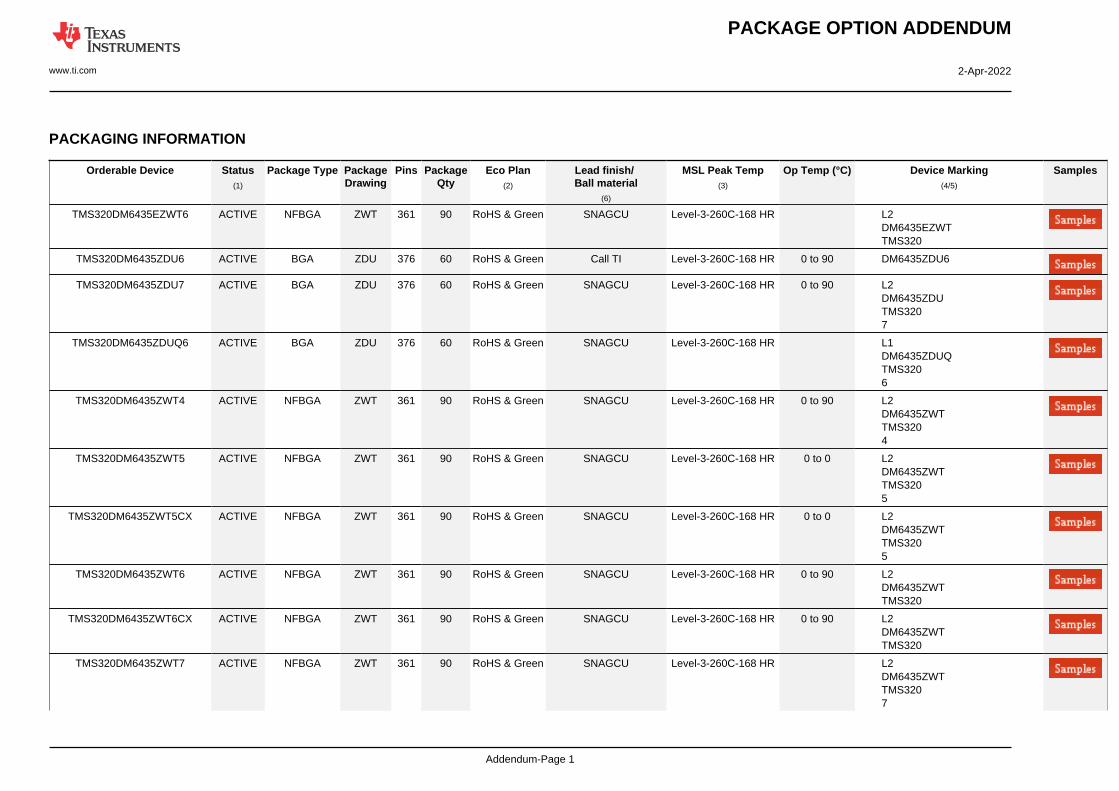
PACKAGE OPTION ADDENDUM
www.ti.com 2-Apr-2022
Addendum-Page 1
PACKAGING INFORMATION
Orderable Device Status(1)
Package Type PackageDrawing
Pins PackageQty
Eco Plan(2)
Lead finish/Ball material
(6)
MSL Peak Temp(3)
Op Temp (°C) Device Marking(4/5)
Samples
TMS320DM6435EZWT6 ACTIVE NFBGA ZWT 361 90 RoHS & Green SNAGCU Level-3-260C-168 HR L2DM6435EZWTTMS320
TMS320DM6435ZDU6 ACTIVE BGA ZDU 376 60 RoHS & Green Call TI Level-3-260C-168 HR 0 to 90 DM6435ZDU6
TMS320DM6435ZDU7 ACTIVE BGA ZDU 376 60 RoHS & Green SNAGCU Level-3-260C-168 HR 0 to 90 L2DM6435ZDUTMS3207
TMS320DM6435ZDUQ6 ACTIVE BGA ZDU 376 60 RoHS & Green SNAGCU Level-3-260C-168 HR L1DM6435ZDUQTMS3206
TMS320DM6435ZWT4 ACTIVE NFBGA ZWT 361 90 RoHS & Green SNAGCU Level-3-260C-168 HR 0 to 90 L2DM6435ZWTTMS3204
TMS320DM6435ZWT5 ACTIVE NFBGA ZWT 361 90 RoHS & Green SNAGCU Level-3-260C-168 HR 0 to 0 L2DM6435ZWTTMS3205
TMS320DM6435ZWT5CX ACTIVE NFBGA ZWT 361 90 RoHS & Green SNAGCU Level-3-260C-168 HR 0 to 0 L2DM6435ZWTTMS3205
TMS320DM6435ZWT6 ACTIVE NFBGA ZWT 361 90 RoHS & Green SNAGCU Level-3-260C-168 HR 0 to 90 L2DM6435ZWTTMS320
TMS320DM6435ZWT6CX ACTIVE NFBGA ZWT 361 90 RoHS & Green SNAGCU Level-3-260C-168 HR 0 to 90 L2DM6435ZWTTMS320
TMS320DM6435ZWT7 ACTIVE NFBGA ZWT 361 90 RoHS & Green SNAGCU Level-3-260C-168 HR L2DM6435ZWTTMS3207
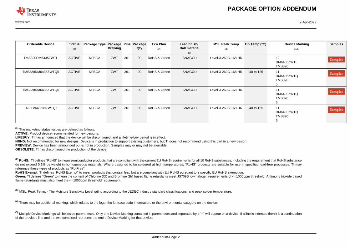
PACKAGE OPTION ADDENDUM
www.ti.com 2-Apr-2022
Addendum-Page 2
Orderable Device Status(1)
Package Type PackageDrawing
Pins PackageQty
Eco Plan(2)
Lead finish/Ball material
(6)
MSL Peak Temp(3)
Op Temp (°C) Device Marking(4/5)
Samples
TMS320DM6435ZWTL ACTIVE NFBGA ZWT 361 90 RoHS & Green SNAGCU Level-3-260C-168 HR L2DM6435ZWTLTMS320
TMS320DM6435ZWTQ5 ACTIVE NFBGA ZWT 361 90 RoHS & Green SNAGCU Level-3-260C-168 HR -40 to 125 L1DM6435ZWTQTMS3205
TMS320DM6435ZWTQ6 ACTIVE NFBGA ZWT 361 90 RoHS & Green SNAGCU Level-3-260C-168 HR L1DM6435ZWTQTMS3206
TNETV6435INZWTQ5 ACTIVE NFBGA ZWT 361 90 RoHS & Green SNAGCU Level-3-260C-168 HR -40 to 125 L1DM6435ZWTQTMS3205
(1) The marketing status values are defined as follows:ACTIVE: Product device recommended for new designs.LIFEBUY: TI has announced that the device will be discontinued, and a lifetime-buy period is in effect.NRND: Not recommended for new designs. Device is in production to support existing customers, but TI does not recommend using this part in a new design.PREVIEW: Device has been announced but is not in production. Samples may or may not be available.OBSOLETE: TI has discontinued the production of the device.
(2) RoHS: TI defines "RoHS" to mean semiconductor products that are compliant with the current EU RoHS requirements for all 10 RoHS substances, including the requirement that RoHS substancedo not exceed 0.1% by weight in homogeneous materials. Where designed to be soldered at high temperatures, "RoHS" products are suitable for use in specified lead-free processes. TI mayreference these types of products as "Pb-Free".RoHS Exempt: TI defines "RoHS Exempt" to mean products that contain lead but are compliant with EU RoHS pursuant to a specific EU RoHS exemption.Green: TI defines "Green" to mean the content of Chlorine (Cl) and Bromine (Br) based flame retardants meet JS709B low halogen requirements of <=1000ppm threshold. Antimony trioxide basedflame retardants must also meet the <=1000ppm threshold requirement.
(3) MSL, Peak Temp. - The Moisture Sensitivity Level rating according to the JEDEC industry standard classifications, and peak solder temperature.
(4) There may be additional marking, which relates to the logo, the lot trace code information, or the environmental category on the device.
(5) Multiple Device Markings will be inside parentheses. Only one Device Marking contained in parentheses and separated by a "~" will appear on a device. If a line is indented then it is a continuationof the previous line and the two combined represent the entire Device Marking for that device.
PACKAGE OPTION ADDENDUM
www.ti.com 2-Apr-2022
Addendum-Page 3
(6) Lead finish/Ball material - Orderable Devices may have multiple material finish options. Finish options are separated by a vertical ruled line. Lead finish/Ball material values may wrap to twolines if the finish value exceeds the maximum column width.
Important Information and Disclaimer:The information provided on this page represents TI's knowledge and belief as of the date that it is provided. TI bases its knowledge and belief on informationprovided by third parties, and makes no representation or warranty as to the accuracy of such information. Efforts are underway to better integrate information from third parties. TI has taken andcontinues to take reasonable steps to provide representative and accurate information but may not have conducted destructive testing or chemical analysis on incoming materials and chemicals.TI and TI suppliers consider certain information to be proprietary, and thus CAS numbers and other limited information may not be available for release.
In no event shall TI's liability arising out of such information exceed the total purchase price of the TI part(s) at issue in this document sold by TI to Customer on an annual basis.
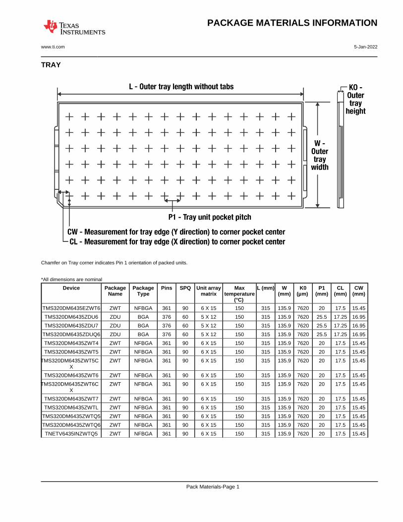
TRAY
Chamfer on Tray corner indicates Pin 1 orientation of packed units.
*All dimensions are nominal
Device PackageName
PackageType
Pins SPQ Unit arraymatrix
Maxtemperature
(°C)
L (mm) W(mm)
K0(µm)
P1(mm)
CL(mm)
CW(mm)
TMS320DM6435EZWT6 ZWT NFBGA 361 90 6 X 15 150 315 135.9 7620 20 17.5 15.45
TMS320DM6435ZDU6 ZDU BGA 376 60 5 X 12 150 315 135.9 7620 25.5 17.25 16.95
TMS320DM6435ZDU7 ZDU BGA 376 60 5 X 12 150 315 135.9 7620 25.5 17.25 16.95
TMS320DM6435ZDUQ6 ZDU BGA 376 60 5 X 12 150 315 135.9 7620 25.5 17.25 16.95
TMS320DM6435ZWT4 ZWT NFBGA 361 90 6 X 15 150 315 135.9 7620 20 17.5 15.45
TMS320DM6435ZWT5 ZWT NFBGA 361 90 6 X 15 150 315 135.9 7620 20 17.5 15.45
TMS320DM6435ZWT5CX
ZWT NFBGA 361 90 6 X 15 150 315 135.9 7620 20 17.5 15.45
TMS320DM6435ZWT6 ZWT NFBGA 361 90 6 X 15 150 315 135.9 7620 20 17.5 15.45
TMS320DM6435ZWT6CX
ZWT NFBGA 361 90 6 X 15 150 315 135.9 7620 20 17.5 15.45
TMS320DM6435ZWT7 ZWT NFBGA 361 90 6 X 15 150 315 135.9 7620 20 17.5 15.45
TMS320DM6435ZWTL ZWT NFBGA 361 90 6 X 15 150 315 135.9 7620 20 17.5 15.45
TMS320DM6435ZWTQ5 ZWT NFBGA 361 90 6 X 15 150 315 135.9 7620 20 17.5 15.45
TMS320DM6435ZWTQ6 ZWT NFBGA 361 90 6 X 15 150 315 135.9 7620 20 17.5 15.45
TNETV6435INZWTQ5 ZWT NFBGA 361 90 6 X 15 150 315 135.9 7620 20 17.5 15.45
PACKAGE MATERIALS INFORMATION
www.ti.com 5-Jan-2022
Pack Materials-Page 1
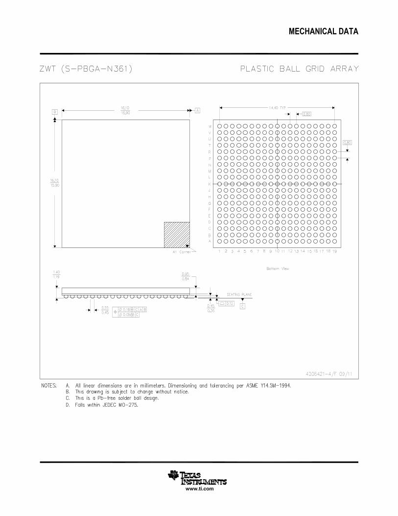
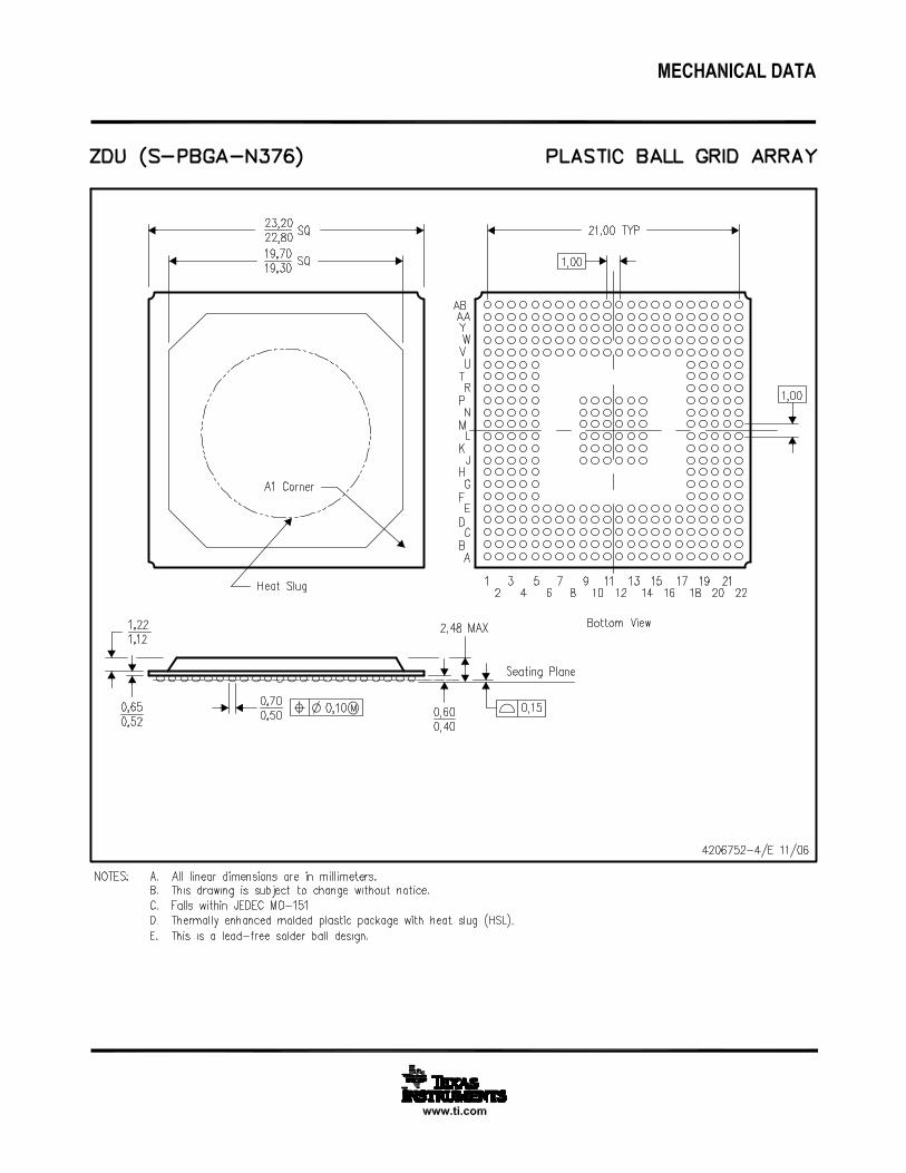

IMPORTANT NOTICE AND DISCLAIMERTI PROVIDES TECHNICAL AND RELIABILITY DATA (INCLUDING DATA SHEETS), DESIGN RESOURCES (INCLUDING REFERENCE DESIGNS), APPLICATION OR OTHER DESIGN ADVICE, WEB TOOLS, SAFETY INFORMATION, AND OTHER RESOURCES “AS IS” AND WITH ALL FAULTS, AND DISCLAIMS ALL WARRANTIES, EXPRESS AND IMPLIED, INCLUDING WITHOUT LIMITATION ANY IMPLIED WARRANTIES OF MERCHANTABILITY, FITNESS FOR A PARTICULAR PURPOSE OR NON-INFRINGEMENT OF THIRD PARTY INTELLECTUAL PROPERTY RIGHTS.These resources are intended for skilled developers designing with TI products. You are solely responsible for (1) selecting the appropriate TI products for your application, (2) designing, validating and testing your application, and (3) ensuring your application meets applicable standards, and any other safety, security, regulatory or other requirements.These resources are subject to change without notice. TI grants you permission to use these resources only for development of an application that uses the TI products described in the resource. Other reproduction and display of these resources is prohibited. No license is granted to any other TI intellectual property right or to any third party intellectual property right. TI disclaims responsibility for, and you will fully indemnify TI and its representatives against, any claims, damages, costs, losses, and liabilities arising out of your use of these resources.TI’s products are provided subject to TI’s Terms of Sale or other applicable terms available either on ti.com or provided in conjunction with such TI products. TI’s provision of these resources does not expand or otherwise alter TI’s applicable warranties or warranty disclaimers for TI products.TI objects to and rejects any additional or different terms you may have proposed. IMPORTANT NOTICE
Mailing Address: Texas Instruments, Post Office Box 655303, Dallas, Texas 75265Copyright © 2022, Texas Instruments Incorporated