tn1236 technical note - stmicroelectronics
TRANSCRIPT
June 2016 DocID029377 Rev 1 1/201
TN1236Technical note
Leadless packages with enhanced board level solder joint reliability for automotive application
AbstractQuad (VFQFN) and dual in line (PowerFLAT™) are very low space occupancy, lead-less packages with enhanced thermal performances. On the purpose to be compliant with automotive reliability requirements, these packages are constructed with Exposed pad and WETTABLE flank that guarantee board level solder joint quality and inspectability. This application note explains stress mechanism on board level soldering joint when subjected to thermal cycling and introduces PCB design guideline to optimize soldering process, thermal performances and hence reliability.
www.st.com
Contents TN1236
2/20 DocID029377 Rev 1
Contents
1 Introduction . . . . . . . . . . . . . . . . . . . . . . . . . . . . . . . . . . . . . . . . . . . . . . . . 5
2 Wettable flank for formation of inspectable solder joint . . . . . . . . . . . . 7
3 Leadless package soldering joint stress mechanism at PCB board level . 9
4 Solder joint reliability characterization . . . . . . . . . . . . . . . . . . . . . . . . . 114.1 Solder join reliability in application. . . . . . . . . . . . . . . . . . . . . . . . . . . . . . 12
5 Optimized PCB design to minimize self- heating induced temperature variations . . . . . . . . . . . . . . . . . . . . . . . . . . . . . . . . . . . . . . . . . . . . . . . . . 145.1 PCB design example and temperature spatial distribution . . . . . . . . . . . . 15
6 Solder fillet to optimize solder joint reliability . . . . . . . . . . . . . . . . . . . 18
7 Revision history . . . . . . . . . . . . . . . . . . . . . . . . . . . . . . . . . . . . . . . . . . . 19
DocID029377 Rev 1 3/20
TN1236 List of tables
3
List of tables
Table 1. Some examples of VFQFN and PowerFLAT™ with lead counts by body size and lead pitch . . 5Table 2. Material characteristics influencing thermo mechanical stress on soldering joints . . . . . . . . 9Table 3. PCB used for thermal simulations. . . . . . . . . . . . . . . . . . . . . . . . . . . . . . . . . . . . . . . . . . . . 16Table 4. Document revision history. . . . . . . . . . . . . . . . . . . . . . . . . . . . . . . . . . . . . . . . . . . . . . . . . . 19
List of figures TN1236
4/20 DocID029377 Rev 1
List of figures
Figure 1. VNQFN package. . . . . . . . . . . . . . . . . . . . . . . . . . . . . . . . . . . . . . . . . . . . . . . . . . . . . . . . . . 5Figure 2. PowerFLAT™ package. . . . . . . . . . . . . . . . . . . . . . . . . . . . . . . . . . . . . . . . . . . . . . . . . . . . . 5Figure 3. Thermal performances versus lead-less package options . . . . . . . . . . . . . . . . . . . . . . . . . . 6Figure 4. VQFN half cut . . . . . . . . . . . . . . . . . . . . . . . . . . . . . . . . . . . . . . . . . . . . . . . . . . . . . . . . . . . 7Figure 5. Side wall plated. . . . . . . . . . . . . . . . . . . . . . . . . . . . . . . . . . . . . . . . . . . . . . . . . . . . . . . . . . . 7Figure 6. Dimpled pad and solder fillet view . . . . . . . . . . . . . . . . . . . . . . . . . . . . . . . . . . . . . . . . . . . . 7Figure 7. Curved punch and solder fillet top view on PowerFLAT™ leads . . . . . . . . . . . . . . . . . . . . . 7Figure 8. Cross cut of solder fillet formation on Half Cut wettable flank option . . . . . . . . . . . . . . . . . . 8Figure 9. Cross section of lead-less package assembled on PCD with simplified explanation of
CTE mismatch induced strengths. . . . . . . . . . . . . . . . . . . . . . . . . . . . . . . . . . . . . . . . . . . . . 9Figure 10. ¼ overall Mesh QFN 8x8 modeling. . . . . . . . . . . . . . . . . . . . . . . . . . . . . . . . . . . . . . . . . . . . 9Figure 11. Accumulated creep strain energy distribution among all solder joints and critical solder joints . 10Figure 12. Thermal cycle @ -40/125 °C, 1 cycle/hour according to JESD22 . . . . . . . . . . . . . . . . . . . 11Figure 13. PowerFLAT™ Solder joint cross sections and crack area evolution with thermal cycling
@ -40°C < T < 125 °C. . . . . . . . . . . . . . . . . . . . . . . . . . . . . . . . . . . . . . . . . . . . . . . . . . . . . 11Figure 14. VNQFN 6x6-40 Solder joint cross section in the middle compared to cross section in the
package corners after 2500 cycles @ -40 °C < T < 125 °C. . . . . . . . . . . . . . . . . . . . . . . . 12Figure 15. Prediction of soldering joint reliability versus ΔTFIELD using modified Coffin-Manson equation 13Figure 16. PCB pattern definition. . . . . . . . . . . . . . . . . . . . . . . . . . . . . . . . . . . . . . . . . . . . . . . . . . . . . 14Figure 17. PCB Thermal Pad and Via Array for 7x7mm, 48 lead and 10x10mm, 68 lead packages . 15Figure 18. Effect of number of VIAS on package thermal performance. . . . . . . . . . . . . . . . . . . . . . . . 15Figure 19. Lay out design for VFQFN 6x6mm 40L . . . . . . . . . . . . . . . . . . . . . . . . . . . . . . . . . . . . . . . 15Figure 20. PCB layers and Cu traces Thickness . . . . . . . . . . . . . . . . . . . . . . . . . . . . . . . . . . . . . . . . . 16Figure 21. Temperature profile around the package @ 2 W power dissipation. . . . . . . . . . . . . . . . . . 17Figure 22. Package Top surface and Mold Hidden temperature @ 2 W power dissipation . . . . . . . . 17Figure 23. Solder fillet dimension definition . . . . . . . . . . . . . . . . . . . . . . . . . . . . . . . . . . . . . . . . . . . . . 18
DocID029377 Rev 1 5/20
TN1236 Introduction
19
1 Introduction
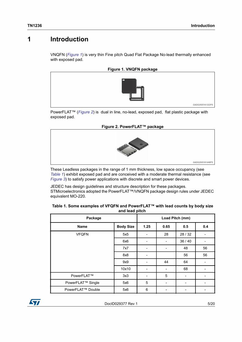
VNQFN (Figure 1) is very thin Fine pitch Quad Flat Package No-lead thermally enhanced with exposed pad.
Figure 1. VNQFN package
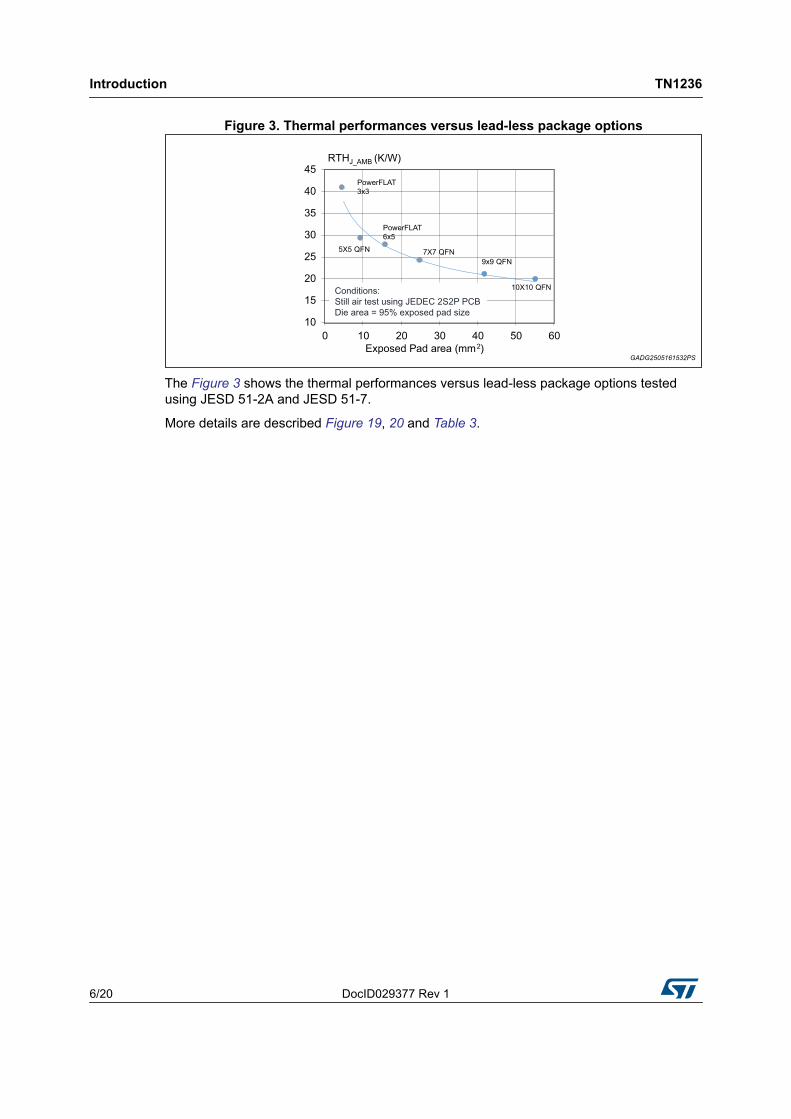
PowerFLAT™ (Figure 2) is dual in line, no-lead, exposed pad, flat plastic package with exposed pad.
Figure 2. PowerFLAT™ package
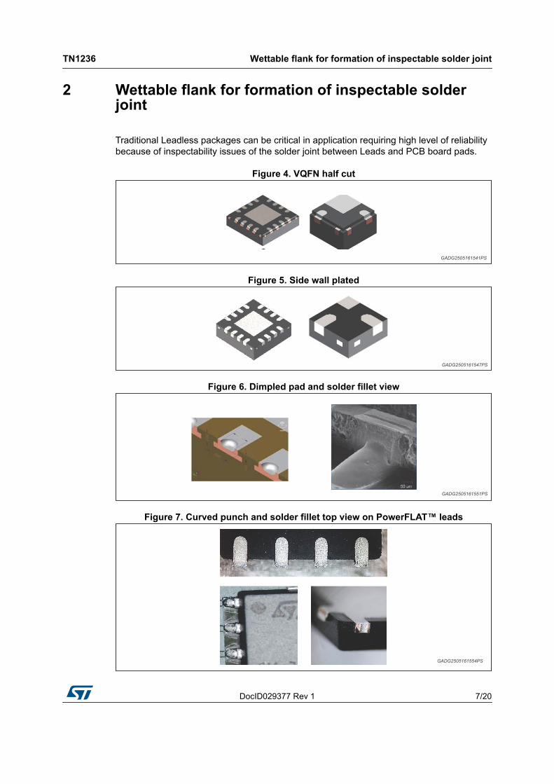
These Leadless packages in the range of 1 mm thickness, low space occupancy (see Table 1) exhibit exposed pad and are conceived with a moderate thermal resistance (see Figure 3) to satisfy power applications with discrete and smart power devices.
JEDEC has design guidelines and structure description for these packages. STMicroelectronics adopted the PowerFLAT™/VNQFN package design rules under JEDEC equivalent MO-220.
Table 1. Some examples of VFQFN and PowerFLAT™ with lead counts by body size and lead pitch
Package Load Pitch (mm)
Name Body Size 1.25 0.65 0.5 0.4
VFQFN 5x5 - 28 28 / 32 -
6x6 - - 36 / 40 -
7x7 - - 48 56
8x8 - 56 56
9x9 - 44 64 -
10x10 - - 68 -
PowerFLAT™ 3x3 - 5 - -
PowerFLAT™ Single 5x6 5 - - -
PowerFLAT™ Double 5x6 6 - - -
Introduction TN1236
6/20 DocID029377 Rev 1
Figure 3. Thermal performances versus lead-less package options
The Figure 3 shows the thermal performances versus lead-less package options tested using JESD 51-2A and JESD 51-7.
More details are described Figure 19, 20 and Table 3.
DocID029377 Rev 1 7/20
TN1236 Wettable flank for formation of inspectable solder joint
19
2 Wettable flank for formation of inspectable solder joint
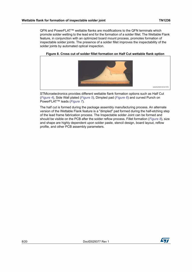
Traditional Leadless packages can be critical in application requiring high level of reliability because of inspectability issues of the solder joint between Leads and PCB board pads.
Figure 4. VQFN half cut
Figure 5. Side wall plated
Figure 6. Dimpled pad and solder fillet view
Figure 7. Curved punch and solder fillet top view on PowerFLAT™ leads
Wettable flank for formation of inspectable solder joint TN1236
8/20 DocID029377 Rev 1
QFN and PowerFLAT™ wettable flanks are modifications to the QFN terminals which promote solder wetting to the lead end for the formation of a solder fillet. The Wettable Flank feature, in conjunction with an optimized board mount process, promotes formation of inspectable solder joints. The presence of a solder fillet improves the inspectability of the solder joints by automated optical inspection.
Figure 8. Cross cut of solder fillet formation on Half Cut wettable flank option
STMicroelectronics provides different wettable flank formation options such as Half Cut (Figure 4), Side Wall plated (Figure 5), Dimpled pad (Figure 6) and curved Punch on PowerFLAT™ leads (Figure 7).
The half cut is formed during the package assembly manufacturing process. An alternate version of the Wettable Flank feature is a "dimpled" pad formed during the half-etching step of the lead frame fabrication process. The Inspectable solder Joint can be formed and should be visible on the PCB after the solder reflow process. Fillet formation (Figure 8), size and shape are highly dependent upon solder paste, stencil design, board layout, reflow profile, and other PCB assembly parameters.
DocID029377 Rev 1 9/20
TN1236 Leadless package soldering joint stress mechanism at PCB board level
19
3 Leadless package soldering joint stress mechanism at PCB board level
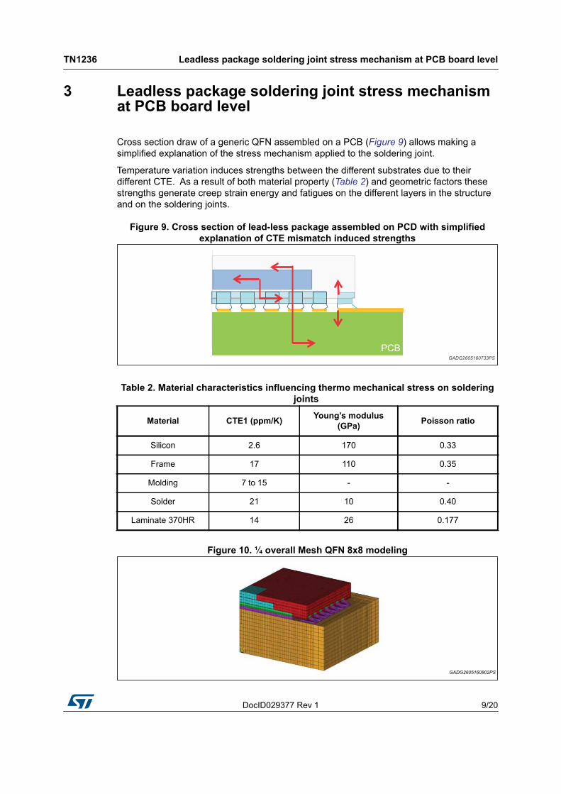
Cross section draw of a generic QFN assembled on a PCB (Figure 9) allows making a simplified explanation of the stress mechanism applied to the soldering joint.
Temperature variation induces strengths between the different substrates due to their different CTE. As a result of both material property (Table 2) and geometric factors these strengths generate creep strain energy and fatigues on the different layers in the structure and on the soldering joints.
Figure 9. Cross section of lead-less package assembled on PCD with simplified explanation of CTE mismatch induced strengths
Figure 10. ¼ overall Mesh QFN 8x8 modeling
Table 2. Material characteristics influencing thermo mechanical stress on soldering joints
Material CTE1 (ppm/K) Young’s modulus (GPa) Poisson ratio
Silicon 2.6 170 0.33
Frame 17 110 0.35
Molding 7 to 15 - -
Solder 21 10 0.40
Laminate 370HR 14 26 0.177
Leadless package soldering joint stress mechanism at PCB board level TN1236
10/20 DocID029377 Rev 1
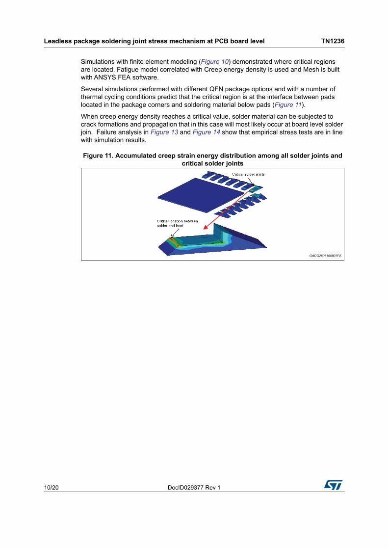
Simulations with finite element modeling (Figure 10) demonstrated where critical regions are located. Fatigue model correlated with Creep energy density is used and Mesh is built with ANSYS FEA software.
Several simulations performed with different QFN package options and with a number of thermal cycling conditions predict that the critical region is at the interface between pads located in the package corners and soldering material below pads (Figure 11).
When creep energy density reaches a critical value, solder material can be subjected to crack formations and propagation that in this case will most likely occur at board level solder join. Failure analysis in Figure 13 and Figure 14 show that empirical stress tests are in line with simulation results.
Figure 11. Accumulated creep strain energy distribution among all solder joints and critical solder joints
DocID029377 Rev 1 11/20
TN1236 Solder joint reliability characterization
19
4 Solder joint reliability characterization
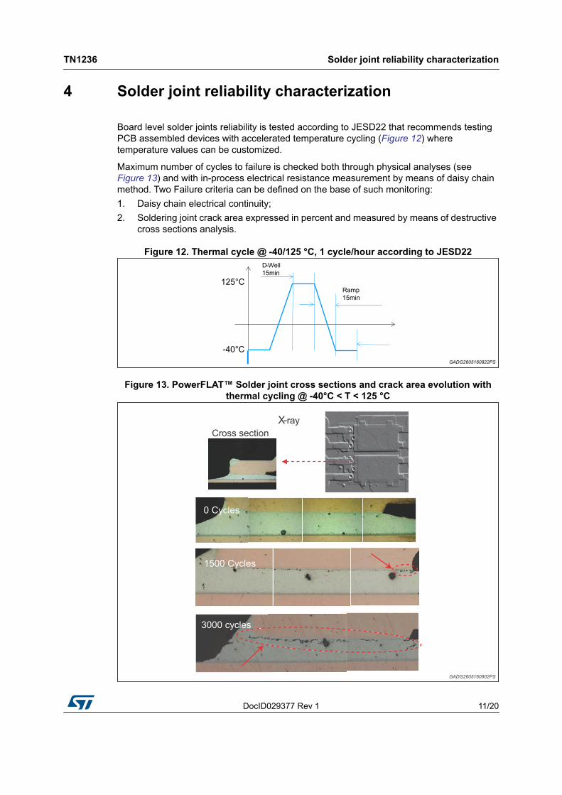
Board level solder joints reliability is tested according to JESD22 that recommends testing PCB assembled devices with accelerated temperature cycling (Figure 12) where temperature values can be customized.
Maximum number of cycles to failure is checked both through physical analyses (see Figure 13) and with in-process electrical resistance measurement by means of daisy chain method. Two Failure criteria can be defined on the base of such monitoring:1. Daisy chain electrical continuity;2. Soldering joint crack area expressed in percent and measured by means of destructive
cross sections analysis.
Figure 12. Thermal cycle @ -40/125 °C, 1 cycle/hour according to JESD22
Figure 13. PowerFLAT™ Solder joint cross sections and crack area evolution with thermal cycling @ -40°C < T < 125 °C
Solder joint reliability characterization TN1236
12/20 DocID029377 Rev 1
Figure 13 shows an example of soldering joint crack area measurement on PowerFLAT™ devices where cross section are performed after 0, 1500 and 3000 (-40 °C < T < 125 °C) thermal cycles . Crack areas are respectively 0%, 10% and 80%.
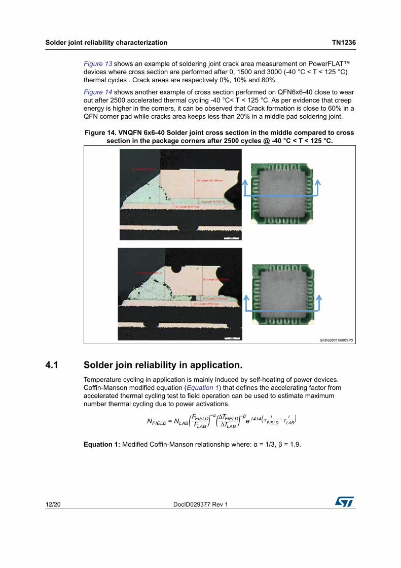
Figure 14 shows another example of cross section performed on QFN6x6-40 close to wear out after 2500 accelerated thermal cycling -40 °C< T < 125 °C. As per evidence that creep energy is higher in the corners, it can be observed that Crack formation is close to 60% in a QFN corner pad while cracks area keeps less than 20% in a middle pad soldering joint.
Figure 14. VNQFN 6x6-40 Solder joint cross section in the middle compared to cross section in the package corners after 2500 cycles @ -40 °C < T < 125 °C.
4.1 Solder join reliability in application.Temperature cycling in application is mainly induced by self-heating of power devices. Coffin-Manson modified equation (Equation 1) that defines the accelerating factor from accelerated thermal cycling test to field operation can be used to estimate maximum number thermal cycling due to power activations.
Equation 1: Modified Coffin-Manson relationship where: α = 1/3, β = 1.9.

DocID029377 Rev 1 13/20
TN1236 Solder joint reliability characterization
19
Figure 15 shows an example where number of thermal cycles to failure is calculated using the following set of parameters: ΔTLAB = 165K correspond to ATC -40°C < T < 125 °C with JESD22 standard; TFIELD = TAMB + ΔTFIELD is the maximum temperature of the soldering joint due to self-
heating of the power device in the application; ΔTFIELD = TFIELD - TAMB. Where TAMB should be defined upon the mission profile
(25 °C, 60 °C were used); NLAB =1000 cycles: it is the number of cycles to guarantee a cracking extension < 20%; NFIELD is the predicted number of cycles with application conditions; FFIELD and FLAB express application and testing frequencies.
Figure 15. Prediction of soldering joint reliability versus ΔTFIELD using modified Coffin-Manson equation
Note: This example is given for illustration. The Coffin-Manson predictions are generally recognized as "conservative" or pessimistic to predict failures under most long term use conditions.For specific case it is recommended to ask support to STMicroelectronics representatives.Increased reliability is expected in the next QFN qualification release.
It also must be noted that temperature in application conditions is not uniform across the package and across PCB sections. The choice to use junction temperature for reliability prediction will be far conservative, so it is suggested to use board level solder joint temperature for more precise prediction.
And it is recommended to minimize temperature cycling by maximizing heat conduction through VIAS and Cu traces on the PCB.

Optimized PCB design to minimize self- heating induced temperature variations TN1236
14/20 DocID029377 Rev 1
5 Optimized PCB design to minimize self- heating induced temperature variations
PowerFLAT™ and QFN with exposed pad are designed to provide a superior thermal performance. This is partly achieved by incorporating an exposed die paddle on the bottom surface of the package. However, in order to take full advantage of this feature, the PCB must be designed to effectively conduct heat away from the package and from the PCB itself. This can be achieved by incorporating thermal pad and thermal vias on the PCB.
Normally, the size of the thermal pad should at least match the exposed die paddle size.
However, depending upon the die paddle size, this size needs to be modified in some cases to avoid solder bridging between thermal pad and the perimeter pads. This is done by defining a clearance between the outer edges of the thermal pad and the inner edges of perimeter pads. This clearance is defined as CPL in Figure 16 and is fixed as 0.15 mm here.
With this constraint, the maximum size of the thermal pad is calculated by Equation 2.
Equation 2: D2’TH = Gmin - 2CPL.
In order to effectively transfer heat from the top metal layer of the PCB to the inner or bottom layers, thermal vias need to be incorporated into the thermal pad design. Although more thermal VIAS improve the package thermal performance, there is a point of diminishing returns (Figure 18). Based on this, it is recommended that an array of thermal vias should be incorporated at 1.0 to 1.2 mm pitch with diameter of 0.3 to 0.33 mm. Representative of these arrays are shown in Figure 17.
Figure 16. PCB pattern definition

DocID029377 Rev 1 15/20
TN1236 Optimized PCB design to minimize self- heating induced temperature variations
19
Figure 17. PCB Thermal Pad and Via Array for 7x7mm, 48 lead and 10x10mm, 68 lead packages
Figure 18. Effect of number of VIAS on package thermal performance
5.1 PCB design example and temperature spatial distributionExample of thermal behavior across QFN and PCB is evaluated with a design reference. Figure 19 shows thermal pad and thermal Vias layout according to the rules defined in the chapter above.
Figure 19. Lay out design for VFQFN 6x6mm 40L
Optimized PCB design to minimize self- heating induced temperature variations TN1236
16/20 DocID029377 Rev 1
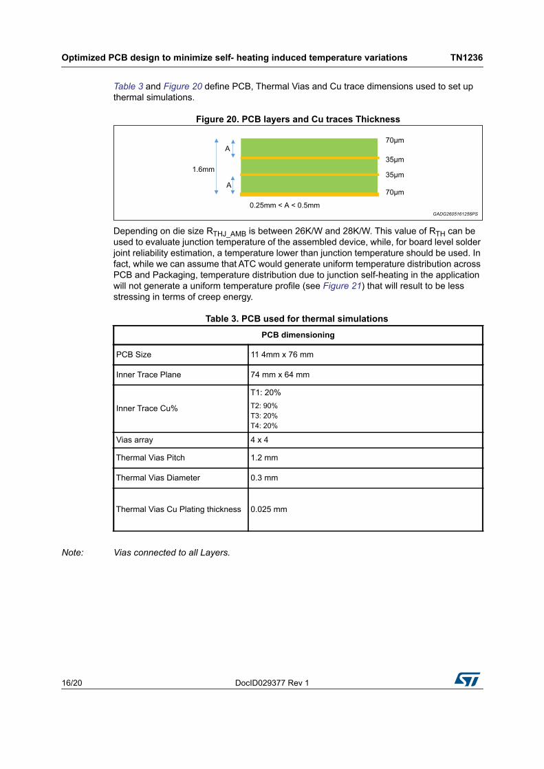
Table 3 and Figure 20 define PCB, Thermal Vias and Cu trace dimensions used to set up thermal simulations.
Figure 20. PCB layers and Cu traces Thickness
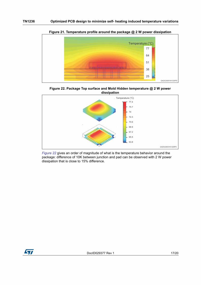
Depending on die size RTHJ_AMB is between 26K/W and 28K/W. This value of RTH can be used to evaluate junction temperature of the assembled device, while, for board level solder joint reliability estimation, a temperature lower than junction temperature should be used. In fact, while we can assume that ATC would generate uniform temperature distribution across PCB and Packaging, temperature distribution due to junction self-heating in the application will not generate a uniform temperature profile (see Figure 21) that will result to be less stressing in terms of creep energy.
Note: Vias connected to all Layers.
Table 3. PCB used for thermal simulations PCB dimensioning
PCB Size 11 4mm x 76 mm
Inner Trace Plane 74 mm x 64 mm
Inner Trace Cu%
T1: 20%T2: 90%T3: 20%T4: 20%
Vias array 4 x 4
Thermal Vias Pitch 1.2 mm
Thermal Vias Diameter 0.3 mm
Thermal Vias Cu Plating thickness 0.025 mm
DocID029377 Rev 1 17/20
TN1236 Optimized PCB design to minimize self- heating induced temperature variations
19
Figure 21. Temperature profile around the package @ 2 W power dissipation
Figure 22. Package Top surface and Mold Hidden temperature @ 2 W power dissipation
Figure 22 gives an order of magnitude of what is the temperature behavior around the package: difference of 10K between junction and pad can be observed with 2 W power dissipation that is close to 15% difference.
Solder fillet to optimize solder joint reliability TN1236
18/20 DocID029377 Rev 1
6 Solder fillet to optimize solder joint reliability
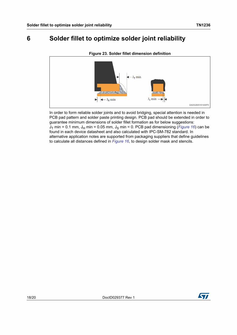
Figure 23. Solder fillet dimension definition
In order to form reliable solder joints and to avoid bridging, special attention is needed in PCB pad pattern and solder paste printing design. PCB pad should be extended in order to guarantee minimum dimensions of solder fillet formation as for below suggestions: JT min = 0.1 mm, JH min = 0.05 mm, JS min = 0. PCB pad dimensioning (Figure 16) can be found in each device datasheet and also calculated with IPC-SM-782 standard. In alternative application notes are supported from packaging suppliers that define guidelines to calculate all distances defined in Figure 16, to design solder mask and stencils.
DocID029377 Rev 1 19/20
TN1236 Revision history
19
7 Revision history
Table 4. Document revision historyDate Revision Changes
17-Jun-2016 1 Initial release.

TN1236
20/20 DocID029377 Rev 1
IMPORTANT NOTICE – PLEASE READ CAREFULLY
STMicroelectronics NV and its subsidiaries (“ST”) reserve the right to make changes, corrections, enhancements, modifications, and improvements to ST products and/or to this document at any time without notice. Purchasers should obtain the latest relevant information on ST products before placing orders. ST products are sold pursuant to ST’s terms and conditions of sale in place at the time of order acknowledgement.
Purchasers are solely responsible for the choice, selection, and use of ST products and ST assumes no liability for application assistance or the design of Purchasers’ products.
No license, express or implied, to any intellectual property right is granted by ST herein.
Resale of ST products with provisions different from the information set forth herein shall void any warranty granted by ST for such product.
ST and the ST logo are trademarks of ST. All other product or service names are the property of their respective owners.
Information in this document supersedes and replaces information previously supplied in any prior versions of this document.
© 2016 STMicroelectronics – All rights reserved