today we test the clickers again. we now venture into the world of metals metals
TRANSCRIPT

Today we test the clickers
again

We now venture into the world of
Metals

Metallic xl Structures
1) Face-Centered Cubic (FCC)
2) Body-Centered Cubic (BCC)
3) Hexagonal Close-Packed (HCP)

FCCAtoms at 8 corners & 6 faces
Equivalent of ? whole atoms.
Atomic Packing Factor (APF)= .74
Fig. 3.1

FCC Cubic structure
STM of PlatinumDept. Kings.edu/chemlab, Property of IBM

A scanning tunneling microscope (STM) is an instrument for imaging surfaces at the atomic level.
What’s an STM image?

Atoms….
You are under our control!

• 1990: IBM scientist Don Eigler used an STM to move single xenon atoms on a nickel surface
•The engineers moved 35 atoms to spell out "IBM" in a 10 micrometer logo.

FCC examples
Lab-grown copper (SEM)0.3 mm
Etched Aluminum (SEM)
GoldGalena (Pb ore)

A scanning electron microscope (SEM) produces images by scanning a sample with a focused beam of electrons. Yields topography and composition.
What’s an SEM image?

BCC
Atoms at 8 corners & 1 in center of
cube
Equivalent of ? whole atoms
APF = .68Fig. 3.2
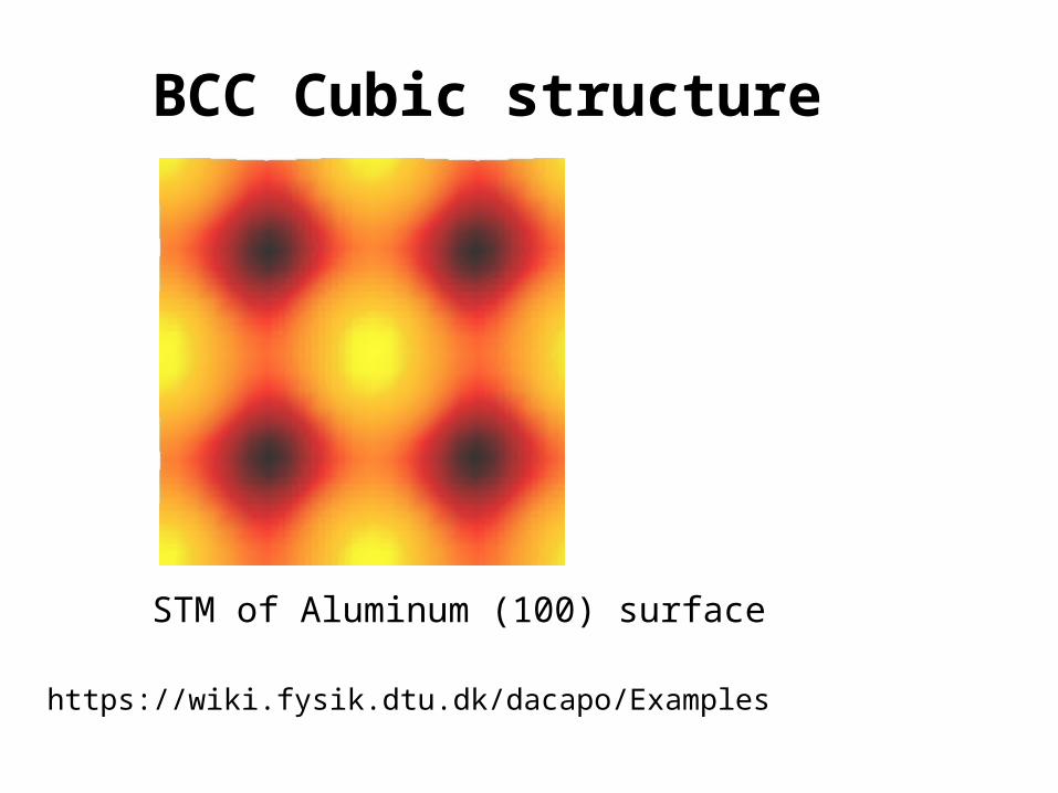
BCC Cubic structure
STM of Aluminum (100) surface
https://wiki.fysik.dtu.dk/dacapo/Examples

BCC examples
Molybdenum Iron

HexagonalSystem
a1 = a2 = a3 ≠ z
º
º
Fig. 3.7

HCP
Atoms at 12 corners, 3 in interior, 2 centered on basal planes
Equivalent of ? whole atoms
(APF)= .74Fig. 3.3

Hexagonal structure
STM of Nickel surface structure.
Dept. Kings.edu/chemlab, Property of IBM

Zinc hand sample
Hexagonal structure

SEM of Fine Cadmium powder
http://www.sciencephoto.com/media/8998/enlarge
SEM of ZnO nanowireshttp://www.lac.tu-clausthal.de/en/arbeitsgruppen/angewandte-photonik-
lac/projekte/zinc-oxide-nanowires-for-photonic-applications/
Hexagonal structure

HCP Examples
Titanium crystals
Cadmium crystal bar
Magnesium (SEM)

Atomic Packing Factors
BCC = 0.68 FCC = 0.74 HCP = 0.74

Metallic xl Structures
Body-Centered Cubic (BCC) APF = 0.68
Na, Fe, Cr, Mo, W
Face-Centered Cubic (FCC) APF = 0.74
Cu, Al, Ag, Au, Pb, Ni, Pt
Hexagonal Close-Packed (HCP) APF = 0.74
Ti, Zn, Cd, Co, Mg

Crystallographic Directions
Section 3.9

Crystallographic direction
A vector between two points in a crystal.
Example:y
x
z
Unit cube

And I should know this because….

Helps us communicate about crystals no matter where we
are in the world…

A systematic study of symmetric tilt-boundaries in hard-sphere f.c.c. crystals
Abstract
A new method is developed for the search of mechanically stable
configurations of symmetric tilt boundaries in hard sphere f.c.c.
crystals. The problem of finding out relative displacements which
minimize the total volume of two crystal blocks forming a boundary, is
simplified to a problem of positioning a single atom sphere relative to a
block which consists of real and “image” atoms; the latter are placed in
such a way to reflect the arrangement in the other crystal block. The
method (the image atom method) has been applied to the analysis of
symmetric coincidence boundaries with [100], [110] and [111] tilt axes
with ∑-values 3–103. For the [100] (013)∑5 boundary, the procedure of
the analysis is described in detail; the derived structures are compared
with those by computer simulation. Numerical data are given in
tabulated forms for some boundaries.

Steps for finding
Crystallographic
Directions

Examples
yx
z
Unit cube
x
z
y
y
x
z
y
x
z
1 2
3 4

Family of Directions
In the same family:
Vector 1
Vector 2
y
x
z
Unit cube
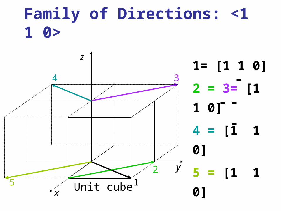
Family of Directions: <1 1 0>
y
x
z
Unit cube
1= [1 1 0]
2 = 3= [1 1 0]
4 = [1 1 0]
5 = [1 1 0]
4 3
12
5

• Structurally equivalent
• Atomic packing is equivalent
Family of Directions: <1 1 0>

• Structurally equivalent
• Atomic packing is equivalent
Family of Directions: <1 1 0>

[a1 a2 a3 z]
Vector:[1 0 0 1]
HexagonalCrystallographic directions

Other Directions[ 1 1 0] [ 1 0 2]
[ 1 1 1] [ 2 1 1] [ 2 1 1] [ 0 0 1]
[ 1 0 1]

Wednesday:
Clicker Questions will include finding
Crystallographic Planes and Crystallographic
Directions
Solved Examples posted on Canvas

Section 3.10
Crystallographic
Planes:
Miller Indices

Steps for finding
Crystallographic
Planes

Examples1
2
3
z
x
y

Families of Planes
(100) (010) (001)
{100} {010} {001}

Family of Planes MI: (X Y Z)
Structurally equivalent planes: {X Y Z}

Hexagonal
Crystallographic planes:The basal plane

Other Planes:
( 1 2 3)
(0 0 1) (0 1 1) (1 1 2)
(2 0 1) (1 0 1)

Notation Summary

Solved Examples posted on Canvas:
Files>Assignments, Homework, Extra Credit