toolsand metrologyat the nanoscale
TRANSCRIPT

Tools & Metrology, Feb. 27th, 2012, Santander, Spain
Tools and Metrology at the NanoScale
Gian Bartolo Picotto
Istituto Nazionale di Ricerca Metrologica (INRIM), Italy

Tools & Metrology, Feb. 27th, 2012, Santander, Spain
Outline
� what is nanometrology?
� measurement needs
� instrumentation and material measures
� surface metrology
� traceability
� particle size
� linewidth standards
� high-resolution interferometry
� comparison and normative work
� conclusions

Tools & Metrology, Feb. 27th, 2012, Santander, Spain
"When you can measure what you are speaking about, and
express it in numbers, you know something about it; but when
you can not measure it, when you can not express it in
numbers, your knowledge is a meagre and unsatisfactory kind;
it may be the beginning of knowledge, but you have scarcely, in
your thoughts, advanced to the stage of Science, whatever the
matter may be"
William Thomson (Lord Kelvin)
Tools & Metrology, Feb. 27th, 2012, Santander, Spain
What is nanometrology?
Nanometrology is the science of measurement of the dimensions of
objects or object features, separations or displacements in the range
from 1 nm to 1000 nm
WGDM / DG7, 1998 Meeting
What is nanotechnology ?
Nanotechnology is the understanding and control of matter at
dimensions between approximately 1 and 100 nanometers, where
unique phenomena enable novel applications. Encompassing nanoscale
science, engineering, and technology, nanotechnology involves imaging,
measuring, modeling, and manipulating matter at this length scale.
The National Nanotechnology Initiative (USA)–
http://www.nano.gov/html/facts/whatIsNano.html

Tools & Metrology, Feb. 27th, 2012, Santander, Spain
NNI – Strategic plan - Feb 2011 – Program Component Areas
4 Instrumentation , Research, Metrology, and Standards for
Nanotechnology
R&D pertaining to the tools needed to advance nanotechnology
research and commercialization, including next-generation
instrumentation for characterization, measurement, synthesis, and
design of materials, structures, devices, and systems. Also includes
R&D and other activities related to development of standards, including
standards for nomenclature, materials characterization and testing, and
manufacture.
The National Nanotechnology Initiative (USA)–http://www.nano.gov/sites/default/files/pub_resource/2011_strategic_plan.pdf

Tools & Metrology, Feb. 27th, 2012, Santander, Spain
A
mp
litu
de
0.1
10
100
1
10
100
1
10
1
10 100 1 10 100 1 10 100 1
mm µm nm
nm
µm
mm
Wavelength
Nanotechnology
IC Technology
MEMS
Needs - AW space

Tools & Metrology, Feb. 27th, 2012, Santander, Spain
Instrumentation
• electron Microscopy (SEM, STEM, TEM)
• probe Microscopy (SPM family)
• interference Microscopy
• diffractometry, scatterometry, ellipsometry
• x-ray and spectroscopic techniques
• ………….

Tools & Metrology, Feb. 27th, 2012, Santander, Spain
standards - material measures
� traceability
� measurement techniques
� design
A list (not exhaustive) of available standards can be downloaded from
http://www.nanoscale.de/standards.htm
Tools & Metrology, Feb. 27th, 2012, Santander, Spain
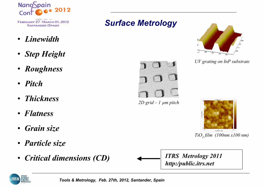
Surface Metrology
• Linewidth
• Step Height
• Roughness
• Pitch
• Thickness
• Flatness
• Grain size
• Particle size
• Critical dimensions (CD)
UV grating on InP substrate
TiO2 film (100nm x100 nm)
ITRS Metrology 2011
http:/public.itrs.net
2D grid – 1 µm pitch

Tools & Metrology, Feb. 27th, 2012, Santander, Spain
Diffractometer
high-accuracy measurements of the pitch of gratings and grids

Tools & Metrology, Feb. 27th, 2012, Santander, Spain
Metrological AFMs - design criteria
• reduced metrology loop
• material
(low CTE, path compensation)
• xyz position/displacement sensors
(interferometric, capacitive, …)
• geometrical effects (Abbé offsets, cosine
error)
• scanner design (range, bandwidth,
straightness, orthogonality, pitch, roll, yaw)
AFM
head
XYZ
scanner

Tools & Metrology, Feb. 27th, 2012, Santander, Spain
geometrical effects
• Abbé
• Cosine
scale length
θθθθtip/sample path
scale length
Abbe
offset
tip path
Tools & Metrology, Feb. 27th, 2012, Santander, Spain
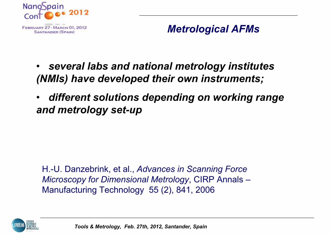
Metrological AFMs
• several labs and national metrology institutes
(NMIs) have developed their own instruments;
• different solutions depending on working range
and metrology set-up
H.-U. Danzebrink, et al., Advances in Scanning Force
Microscopy for Dimensional Metrology, CIRP Annals –
Manufacturing Technology 55 (2), 841, 2006

Tools & Metrology, Feb. 27th, 2012, Santander, Spain
Interference microscopy
Z
PSI – Phase Shifting Interferometry
- step-height < λ/2
- monocromatic sources
- phase interferograms are taken at
given sub-λ steps
VSI – Vertical Scanning Interferometry
- white light or monocromatic sources
- position of the fringe envelop peak is
detected while scanning the vertical axis
- on-board z-metrology
sample
source
interferogram
Tools & Metrology, Feb. 27th, 2012, Santander, Spain
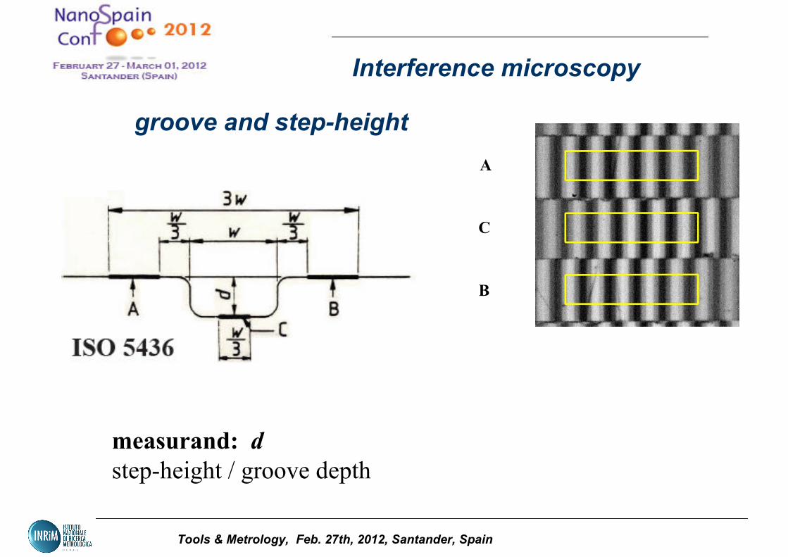
Interference microscopy
groove and step-height
measurand: d
step-height / groove depth
A
C
B

Tools & Metrology, Feb. 27th, 2012, Santander, Spain
AW Space - instrumentation
Am
pli
tud
e
0.1
10
100
1
10
100
1
10
1
10 1001 10 1001 10 1001
mmµmnm
nm
µm
mm
Wavelength
AFM
Optical
Stylus
Surface metrology

Tools & Metrology, Feb. 27th, 2012, Santander, Spain
Traceability chain
step-height standards
SPM
stabilized lasers,
spectral lamps
interference
microscope
autocollimator
Stylus
profilometer
small angle
generator
laser λ filtersmicro/nano
displacement
actuators
lambdameter, spectrometerinterferometry
Tools & Metrology, Feb. 27th, 2012, Santander, Spain
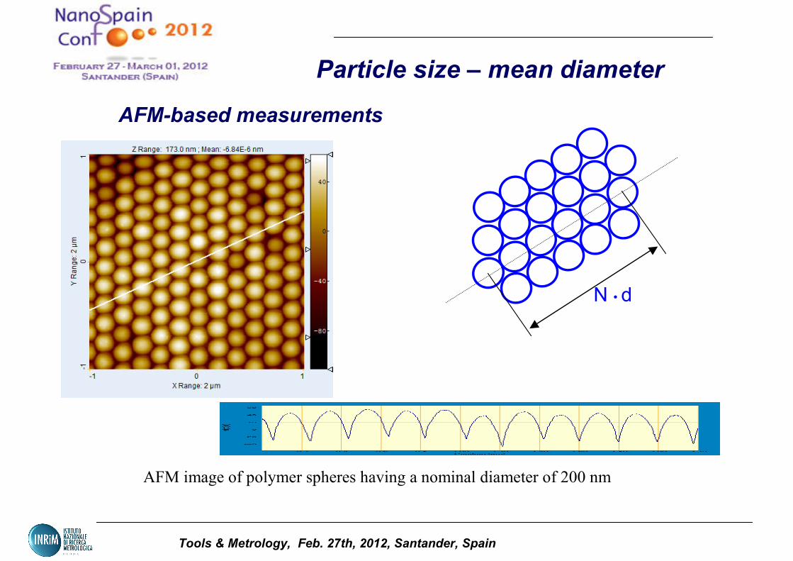
Particle size – mean diameter
AFM image of polymer spheres having a nominal diameter of 200 nm
N • d
AFM-based measurements
Tools & Metrology, Feb. 27th, 2012, Santander, Spain
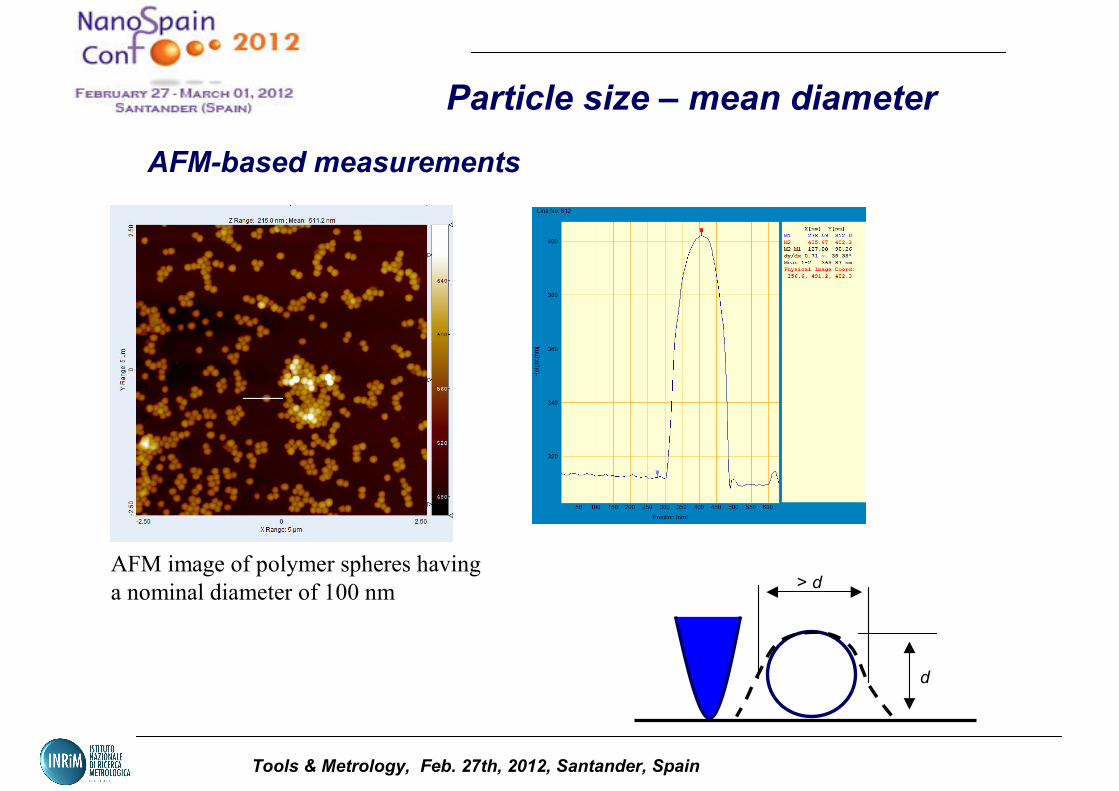
Particle size – mean diameter
AFM image of polymer spheres having
a nominal diameter of 100 nm> d
d
AFM-based measurements

Tools & Metrology, Feb. 27th, 2012, Santander, Spain
Particle size
EURAMET joint research project "Traceable measurement of nanoparticle size"
funded from the European Union's Seventh Framework Programme, ERA-NET
Plus, under Grant Agreement No. 217257
http://www.euramet.org/fileadmin/docs/EMRP/JRP/iMERA-
plus_JRPs_2010-06-22/T3.J1.1.pdf
F. Meli1, et al., Traceable size determination of nanoparticles, a comparison among
European metrology institutes, submitted to Meas. Sci. & Technol.
Tools & Metrology, Feb. 27th, 2012, Santander, Spain
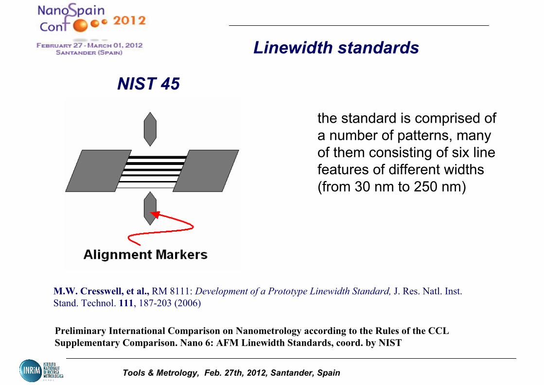
Linewidth standards
Preliminary International Comparison on Nanometrology according to the Rules of the CCL
Supplementary Comparison. Nano 6: AFM Linewidth Standards, coord. by NIST
the standard is comprised of
a number of patterns, many
of them consisting of six line
features of different widths
(from 30 nm to 250 nm)
NIST 45
M.W. Cresswell, et al., RM 8111: Development of a Prototype Linewidth Standard, J. Res. Natl. Inst.
Stand. Technol. 111, 187-203 (2006)
Tools & Metrology, Feb. 27th, 2012, Santander, Spain
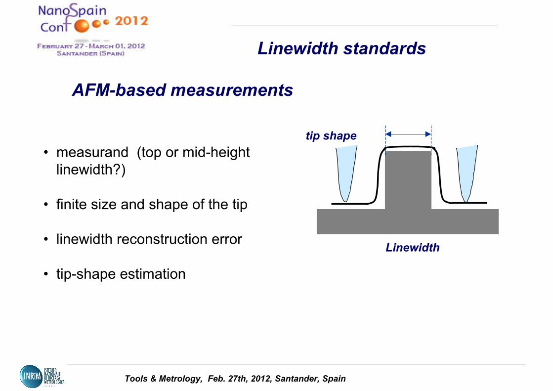
Linewidth standards
AFM-based measurements
• measurand (top or mid-height
linewidth?)
• finite size and shape of the tip
• linewidth reconstruction error
• tip-shape estimation
tip shape
Linewidth
Tools & Metrology, Feb. 27th, 2012, Santander, Spain
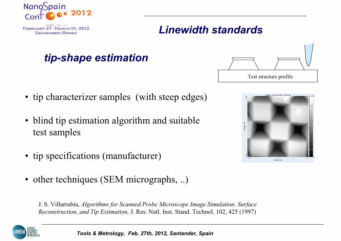
Linewidth standards
tip-shape estimation
• tip characterizer samples (with steep edges)
• blind tip estimation algorithm and suitable
test samples
• tip specifications (manufacturer)
• other techniques (SEM micrographs, ..)
J. S. Villarrubia, Algorithms for Scanned Probe Microscope Image Simulation, Surface
Reconstruction, and Tip Estimation, J. Res. Natl. Inst. Stand. Technol. 102, 425 (1997)
Test structure profile

Tools & Metrology, Feb. 27th, 2012, Santander, Spain
high-resolution interferometry
(position and displacement measurements)
• pattern placement measurements on photomasks
• position control in wafer scanners
• double patterning techniques demands a high
reproducibility in positioning
Needs
Tools & Metrology, Feb. 27th, 2012, Santander, Spain
Interferometry
• geometrical errors (Abbé, cosine)
• ambient (air refractivity, material temperature, optics
thermal drifts, dead-path)
• laser wavelength
• optical non-linearity (fringe-periodical phase error
with sub-wavelength steps)
Error sources
Tools & Metrology, Feb. 27th, 2012, Santander, Spain
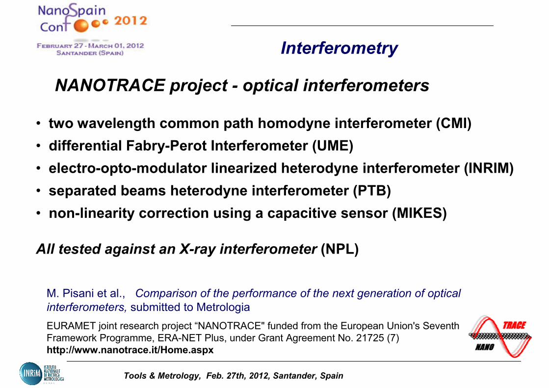
Interferometry
EURAMET joint research project “NANOTRACE" funded from the European Union's Seventh
Framework Programme, ERA-NET Plus, under Grant Agreement No. 21725 (7)
http://www.nanotrace.it/Home.aspx
• two wavelength common path homodyne interferometer (CMI)
• differential Fabry-Perot Interferometer (UME)
• electro-opto-modulator linearized heterodyne interferometer (INRIM)
• separated beams heterodyne interferometer (PTB)
• non-linearity correction using a capacitive sensor (MIKES)
All tested against an X-ray interferometer (NPL)
NANOTRACE project - optical interferometers
M. Pisani et al., Comparison of the performance of the next generation of optical
interferometers, submitted to Metrologia

Tools & Metrology, Feb. 27th, 2012, Santander, Spain
• traceable standards;
• calibrated instruments;
• measurement protocols;
• consistent uncertainty budget;
• written standards and good-practise guides to
ensure the quality of measurements (ISO 17025)
Quantitative Microscopy
ISO/IEC 17025:2005 General requirements for the competence of testing and calibration
laboratories

Tools & Metrology, Feb. 27th, 2012, Santander, Spain
Supplementary Comparisons, Length,
dimensional nanometrology
http://kcdb.bipm.org
• CCL-S1 - Nano 4, lateral, 1D gratings, 290 and 700 nm pitch
• CCL-S2 - Nano 2, step-height, 20 … 800 nm
• CCL-S3 - Nano 3, linescale, 280 mm length
• CCL-S4 - Nano 5, lateral, 2D gratings, 300 and 700 nm pitch
• Nano 6 , linewidth standards < 500 nm, in progress
• EUROMET.L-S15, step-height, 7 ... 2000 nm
• APMP.L-S2, 1D gratings, 50 and 100 nm pitch
Tools & Metrology, Feb. 27th, 2012, Santander, Spain
under development by several standardization organizations
- ISO/TC229 - Nanotechnologies
- CEN/TC352 - Nanotechnologies
- IEC/TC113 - Nanotechnology
- JWGs ISO/TC229 IEC/TC113
- ISO/TC213 – GPS (Geometrical Product Specifications)
WG16 - Surface texture (ISO 25178 – areal texture)
Written Standards

Tools & Metrology, Feb. 27th, 2012, Santander, Spain
Conclusions
• quantitative measurements and traceable standards are
needed to support the overall reliability of products
• several projects have been carried out by national
Metrology Institutes and other labs to extend traceability and
to improve measurement capabilities at the nanoscale
• consistency of measurements is demonstrated and
periodically tested by inter-laboratory comparisons
• an agreed standardization framework is supported by pre-
normative research