tps255x precision adjustable current-limited power
TRANSCRIPT
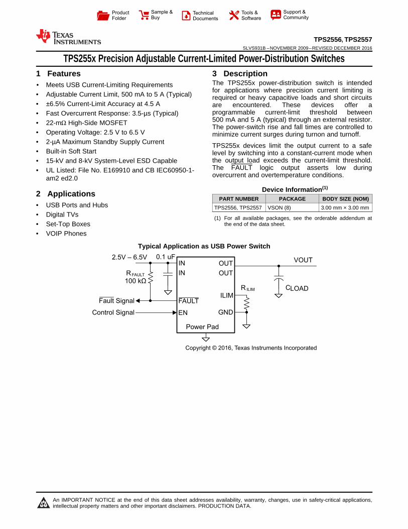
OUT
OUT
IN
IN
GND
FAULTILIM
EN
R ILIM
R FAULT
100 kΩ
Control Signal
2.5V – 6.5V VOUT0.1 uF
CLOAD
Fault Signal
Power Pad
Copyright © 2016, Texas Instruments Incorporated
Product
Folder
Sample &Buy
Technical
Documents
Tools &
Software
Support &Community
An IMPORTANT NOTICE at the end of this data sheet addresses availability, warranty, changes, use in safety-critical applications,intellectual property matters and other important disclaimers. PRODUCTION DATA.
TPS2556, TPS2557SLVS931B –NOVEMBER 2009–REVISED DECEMBER 2016
TPS255x Precision Adjustable Current-Limited Power-Distribution Switches
1
1 Features1• Meets USB Current-Limiting Requirements• Adjustable Current Limit, 500 mA to 5 A (Typical)• ±6.5% Current-Limit Accuracy at 4.5 A• Fast Overcurrent Response: 3.5-µs (Typical)• 22-mΩ High-Side MOSFET• Operating Voltage: 2.5 V to 6.5 V• 2-µA Maximum Standby Supply Current• Built-in Soft Start• 15-kV and 8-kV System-Level ESD Capable• UL Listed: File No. E169910 and CB IEC60950-1-
am2 ed2.0
2 Applications• USB Ports and Hubs• Digital TVs• Set-Top Boxes• VOIP Phones
3 DescriptionThe TPS255x power-distribution switch is intendedfor applications where precision current limiting isrequired or heavy capacitive loads and short circuitsare encountered. These devices offer aprogrammable current-limit threshold between500 mA and 5 A (typical) through an external resistor.The power-switch rise and fall times are controlled tominimize current surges during turnon and turnoff.
TPS255x devices limit the output current to a safelevel by switching into a constant-current mode whenthe output load exceeds the current-limit threshold.The FAULT logic output asserts low duringovercurrent and overtemperature conditions.
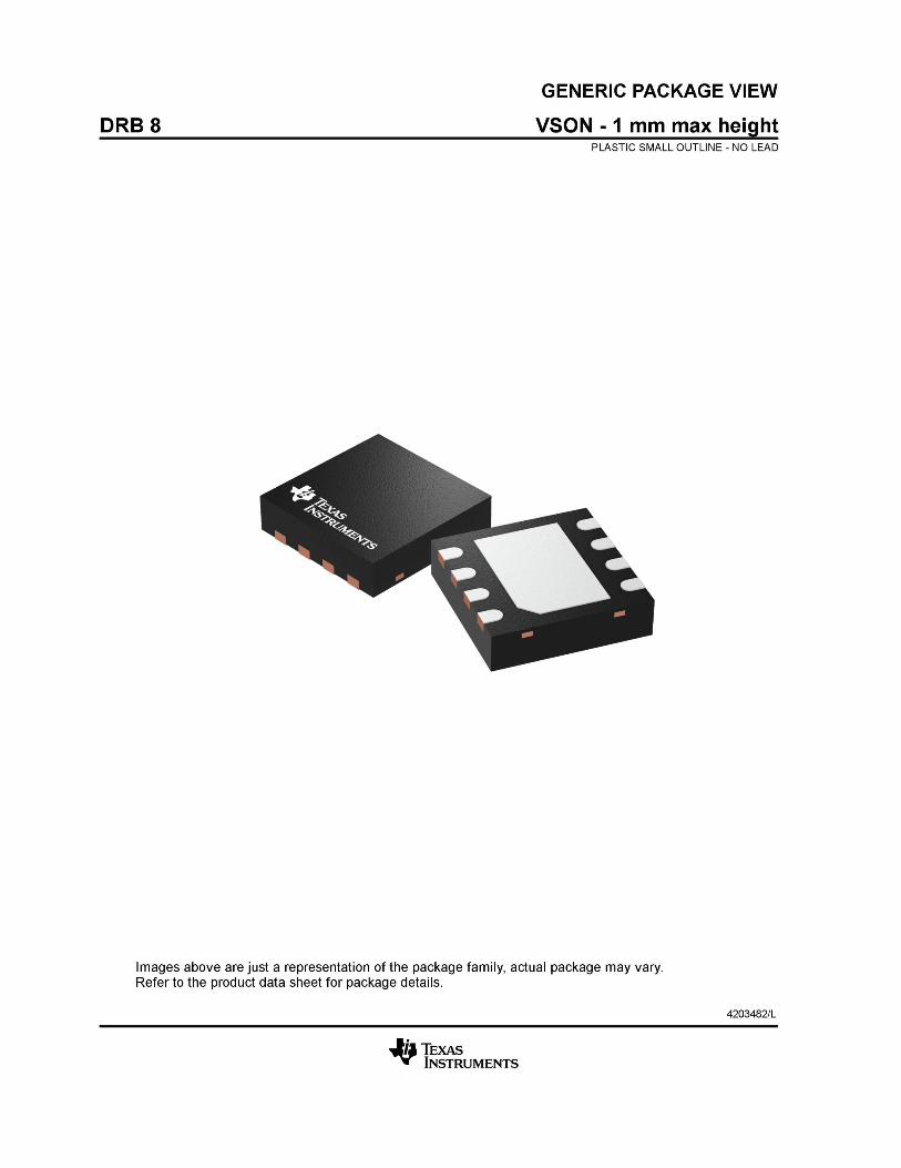
Device Information(1)
PART NUMBER PACKAGE BODY SIZE (NOM)TPS2556, TPS2557 VSON (8) 3.00 mm × 3.00 mm
(1) For all available packages, see the orderable addendum atthe end of the data sheet.
Typical Application as USB Power Switch
2
TPS2556, TPS2557SLVS931B –NOVEMBER 2009–REVISED DECEMBER 2016 www.ti.com
Product Folder Links: TPS2556 TPS2557
Submit Documentation Feedback Copyright © 2009–2016, Texas Instruments Incorporated
Table of Contents1 Features .................................................................. 12 Applications ........................................................... 13 Description ............................................................. 14 Revision History..................................................... 25 Device Comparison Table ..................................... 36 Pin Configuration and Functions ......................... 37 Specifications......................................................... 4
7.1 Absolute Maximum Ratings ...................................... 47.2 ESD Ratings.............................................................. 47.3 Recommended Operating Conditions....................... 47.4 Thermal Information .................................................. 57.5 Electrical Characteristics........................................... 57.6 Switching Characteristics .......................................... 67.7 Typical Characteristics .............................................. 7
8 Parameter Measurement Information ................ 109 Detailed Description ............................................ 11
9.1 Overview ................................................................. 119.2 Functional Block Diagram ....................................... 11
9.3 Feature Description................................................. 119.4 Device Functional Modes........................................ 12
10 Application and Implementation........................ 1310.1 Application Information.......................................... 1310.2 Typical Applications .............................................. 13
11 Power Supply Recommendations ..................... 1812 Layout................................................................... 19
12.1 Layout Guidelines ................................................. 1912.2 Layout Example .................................................... 1912.3 Thermal Considerations ........................................ 20
13 Device and Documentation Support ................. 2113.1 Related Links ........................................................ 2113.2 Receiving Notification of Documentation Updates 2113.3 Community Resources.......................................... 2113.4 Trademarks ........................................................... 2113.5 Electrostatic Discharge Caution............................ 2113.6 Glossary ................................................................ 21
14 Mechanical, Packaging, and OrderableInformation ........................................................... 21
4 Revision HistoryNOTE: Page numbers for previous revisions may differ from page numbers in the current version.
Changes from Revision A (Feburary 2012) to Revision B Page
• Added Device Information table, Device Comparison Table, Pin Configuration and Functions section, Specificationssection, ESD Ratings table, Application and Implementation section, Power Supply Recommendations section,Layout section, Device and Documentation Support section, and Mechanical, Packaging, and Orderable Informationsection .................................................................................................................................................................................... 1
• Deleted Ordering Information table; see Package Option Addendum at the end of the data sheet ...................................... 1• Added Thermal Information table ........................................................................................................................................... 5• Changed RθJC(top) value in Thermal Information table From: 10.7°C/W To: 54.5°C/W........................................................... 5• Changed Figure 11 title From: Current Limit Threshold Vs RILM To: Switch Current vs Drain-Source Voltage Across
Switch ..................................................................................................................................................................................... 7• Changed Figure 12 title From: Current Limit Threshold Vs RILM To: Switch Current vs Drain-Source Voltage Across
Switch ..................................................................................................................................................................................... 7
Changes from Original (November 2009) to Revision A Page
• Changed VEN to VEN in Recommended Operating Conditions table ...................................................................................... 4• Changed VEN to VEN in Recommended Operating Conditions table ...................................................................................... 4
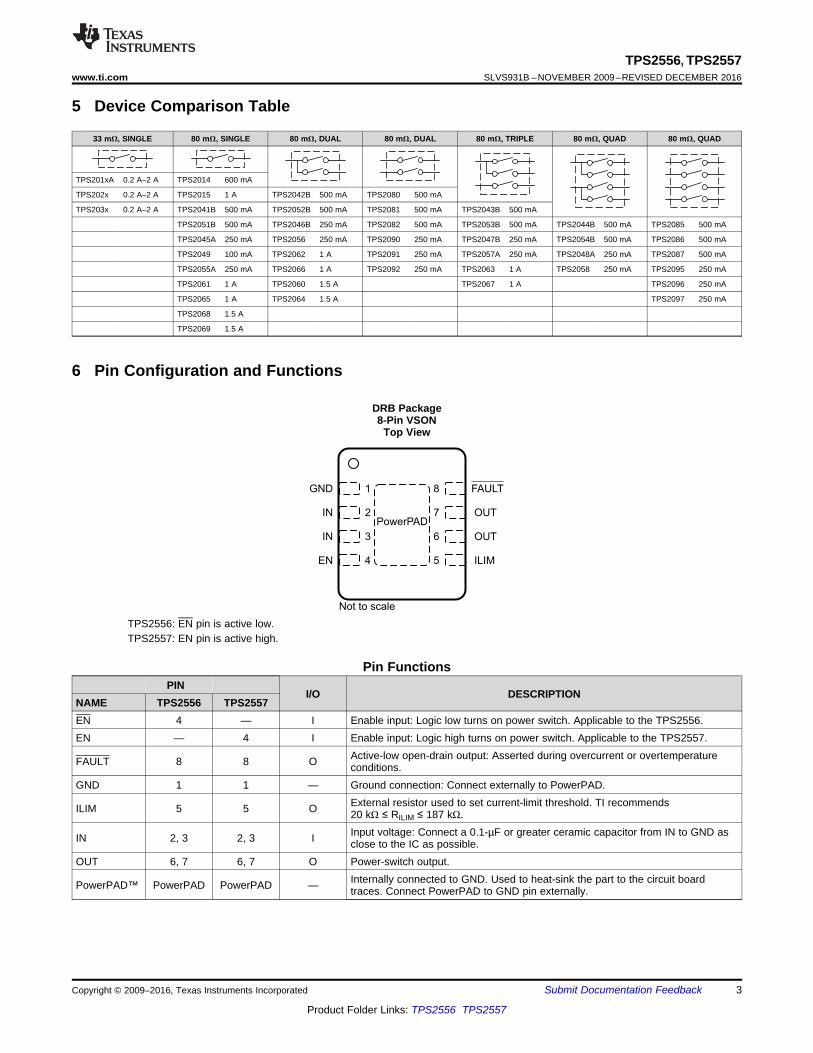
1GND 8 FAULT
2IN 7 OUT
3IN 6 OUT
4EN 5 ILIM
Not to scale
PowerPAD
3
TPS2556, TPS2557www.ti.com SLVS931B –NOVEMBER 2009–REVISED DECEMBER 2016
Product Folder Links: TPS2556 TPS2557
Submit Documentation FeedbackCopyright © 2009–2016, Texas Instruments Incorporated
5 Device Comparison Table
33 mΩ, SINGLE 80 mΩ, SINGLE 80 mΩ, DUAL 80 mΩ, DUAL 80 mΩ, TRIPLE 80 mΩ, QUAD 80 mΩ, QUAD
TPS201xA 0.2 A–2 A TPS2014 600 mA
TPS202x 0.2 A–2 A TPS2015 1 A TPS2042B 500 mA TPS2080 500 mA
TPS203x 0.2 A–2 A TPS2041B 500 mA TPS2052B 500 mA TPS2081 500 mA TPS2043B 500 mA
TPS2051B 500 mA TPS2046B 250 mA TPS2082 500 mA TPS2053B 500 mA TPS2044B 500 mA TPS2085 500 mA
TPS2045A 250 mA TPS2056 250 mA TPS2090 250 mA TPS2047B 250 mA TPS2054B 500 mA TPS2086 500 mA
TPS2049 100 mA TPS2062 1 A TPS2091 250 mA TPS2057A 250 mA TPS2048A 250 mA TPS2087 500 mA
TPS2055A 250 mA TPS2066 1 A TPS2092 250 mA TPS2063 1 A TPS2058 250 mA TPS2095 250 mA
TPS2061 1 A TPS2060 1.5 A TPS2067 1 A TPS2096 250 mA
TPS2065 1 A TPS2064 1.5 A TPS2097 250 mA
TPS2068 1.5 A
TPS2069 1.5 A
6 Pin Configuration and Functions
DRB Package8-Pin VSON
Top View
TPS2556: EN pin is active low.TPS2557: EN pin is active high.
Pin FunctionsPIN
I/O DESCRIPTIONNAME TPS2556 TPS2557EN 4 — I Enable input: Logic low turns on power switch. Applicable to the TPS2556.EN — 4 I Enable input: Logic high turns on power switch. Applicable to the TPS2557.
FAULT 8 8 O Active-low open-drain output: Asserted during overcurrent or overtemperatureconditions.
GND 1 1 — Ground connection: Connect externally to PowerPAD.
ILIM 5 5 O External resistor used to set current-limit threshold. TI recommends20 kΩ ≤ RILIM ≤ 187 kΩ.
IN 2, 3 2, 3 I Input voltage: Connect a 0.1-µF or greater ceramic capacitor from IN to GND asclose to the IC as possible.
OUT 6, 7 6, 7 O Power-switch output.
PowerPAD™ PowerPAD PowerPAD — Internally connected to GND. Used to heat-sink the part to the circuit boardtraces. Connect PowerPAD to GND pin externally.
4
TPS2556, TPS2557SLVS931B –NOVEMBER 2009–REVISED DECEMBER 2016 www.ti.com
Product Folder Links: TPS2556 TPS2557
Submit Documentation Feedback Copyright © 2009–2016, Texas Instruments Incorporated
(1) Stresses beyond those listed under Absolute Maximum Ratings may cause permanent damage to the device. These are stress ratingsonly, which do not imply functional operation of the device at these or any other conditions beyond those indicated under RecommendedOperating Conditions. Exposure to absolute-maximum-rated conditions for extended periods may affect device reliability.
(2) Voltages are referenced to GND unless otherwise noted.
7 Specifications
7.1 Absolute Maximum Ratingsover operating free-air temperature range (unless otherwise noted) (1) (2)
MIN MAX UNITVoltage IN, OUT, EN or EN, ILIM, and FAULT pins –0.3 7 VVoltage from IN to OUT –7 7 VContinuous output current Internally limitedContinuous FAULT sink current 25 mAILIM source current Internally limitedContinuous total power dissipation See Thermal InformationMaximum junction temperature –40 OTSD2 °CStorage temperature, Tstg -65 150 °C
(1) JEDEC document JEP155 states that 500-V HBM allows safe manufacturing with a standard ESD control process.(2) JEDEC document JEP157 states that 250-V CDM allows safe manufacturing with a standard ESD control process.(3) Surges per EN61000-4-2, 1999 applied between USB and output ground of the TPS2556EVM (HPA423) evaluation module (see Using
the TPS2556EVM-423 and TPS2557EVM-423). These were the test levels, not the failure threshold.
7.2 ESD RatingsVALUE UNIT
V(ESD) Electrostatic discharge
Human-body model (HBM), per ANSI/ESDA/JEDEC JS-001 (1) ±2000
VCharged-device model (CDM), per JEDEC specification JESD22-C101 (2) ±500IEC 61000-4-2 contact discharge (3) ±8000IEC 61000-4-2 air discharge (3) ±15000
7.3 Recommended Operating ConditionsMIN MAX UNIT
VIN Input voltage, IN 2.5 6.5 VVEN Enable voltage
TPS2556 0 6.5V
VEN TPS2557 0 6.5VIH High-level input voltage on Enable pin 1.1
VVIL Low-level input voltage on Enable pin 0.66IOUT Continuous output current (OUT pin) 0 5 A
Continuous FAULT sink current 0 10 mARILIM Recommended resistor limit 20 187 kΩTJ Operating virtual junction temperature –40 125 °C
5
TPS2556, TPS2557www.ti.com SLVS931B –NOVEMBER 2009–REVISED DECEMBER 2016
Product Folder Links: TPS2556 TPS2557
Submit Documentation FeedbackCopyright © 2009–2016, Texas Instruments Incorporated
(1) For more information about traditional and new thermal metrics, see the Semiconductor and IC Package Thermal Metrics applicationreport.
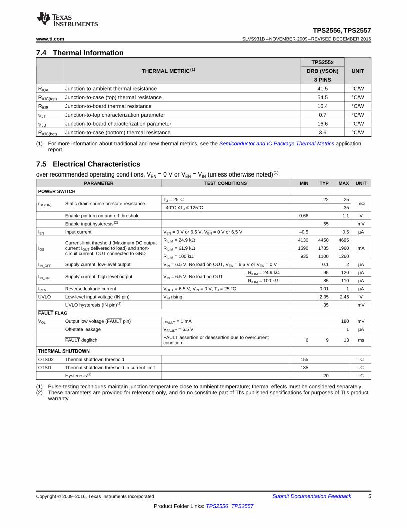
7.4 Thermal Information
THERMAL METRIC (1)TPS255x
UNITDRB (VSON)8 PINS
RθJA Junction-to-ambient thermal resistance 41.5 °C/WRθJC(top) Junction-to-case (top) thermal resistance 54.5 °C/WRθJB Junction-to-board thermal resistance 16.4 °C/WψJT Junction-to-top characterization parameter 0.7 °C/WψJB Junction-to-board characterization parameter 16.6 °C/WRθJC(bot) Junction-to-case (bottom) thermal resistance 3.6 °C/W
(1) Pulse-testing techniques maintain junction temperature close to ambient temperature; thermal effects must be considered separately.(2) These parameters are provided for reference only, and do no constitute part of TI's published specifications for purposes of TI's product
warranty.
7.5 Electrical Characteristicsover recommended operating conditions, VEN = 0 V or VEN = VIN (unless otherwise noted) (1)
PARAMETER TEST CONDITIONS MIN TYP MAX UNIT
POWER SWITCH
rDS(ON) Static drain-source on-state resistanceTJ = 25°C 22 25
mΩ–40°C ≤TJ ≤ 125°C 35
Enable pin turn on and off threshold 0.66 1.1 V
Enable input hysteresis (2) 55 mV
IEN Input current VEN = 0 V or 6.5 V, VEN = 0 V or 6.5 V –0.5 0.5 µA
IOS
Current-limit threshold (Maximum DC outputcurrent IOUT delivered to load) and short-circuit current, OUT connected to GND
RILIM = 24.9 kΩ 4130 4450 4695
mARILIM = 61.9 kΩ 1590 1785 1960
RILIM = 100 kΩ 935 1100 1260
IIN_OFF Supply current, low-level output VIN = 6.5 V, No load on OUT, VEN = 6.5 V or VEN = 0 V 0.1 2 µA
IIN_ON Supply current, high-level output VIN = 6.5 V, No load on OUTRILIM = 24.9 kΩ 95 120 µA
RILIM = 100 kΩ 85 110 µA
IREV Reverse leakage current VOUT = 6.5 V, VIN = 0 V, TJ = 25 °C 0.01 1 µA
UVLO Low-level input voltage (IN pin) VIN rising 2.35 2.45 V
UVLO hysteresis (IN pin) (2) 35 mV
FAULT FLAG
VOL Output low voltage (FAULT pin) IFAULT = 1 mA 180 mV
Off-state leakage VFAULT = 6.5 V 1 µA
FAULT deglitch FAULT assertion or deassertion due to overcurrentcondition 6 9 13 ms
THERMAL SHUTDOWN
OTSD2 Thermal shutdown threshold 155 °C
OTSD Thermal shutdown threshold in current-limit 135 °C
Hysteresis (2) 20 °C
6
TPS2556, TPS2557SLVS931B –NOVEMBER 2009–REVISED DECEMBER 2016 www.ti.com
Product Folder Links: TPS2556 TPS2557
Submit Documentation Feedback Copyright © 2009–2016, Texas Instruments Incorporated
(1) These parameters are provided for reference only, and do no constitute part of TI's published specifications for purposes of TI's productwarranty.
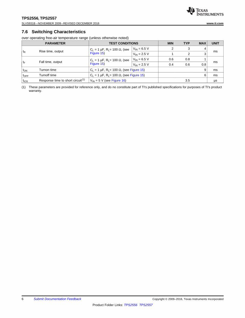
7.6 Switching Characteristicsover operating free-air temperature range (unless otherwise noted)
PARAMETER TEST CONDITIONS MIN TYP MAX UNIT
tR Rise time, output CL = 1 µF, RL= 100 Ω, (seeFigure 15)
VIN = 6.5 V 2 3 4ms
VIN = 2.5 V 1 2 3
tF Fall time, output CL = 1 µF, RL= 100 Ω, (seeFigure 15)
VIN = 6.5 V 0.6 0.8 1ms
VIN = 2.5 V 0.4 0.6 0.8tON Turnon time CL = 1 µF, RL= 100 Ω, (see Figure 15) 9 mstOFF Turnoff time CL = 1 µF, RL= 100 Ω, (see Figure 15) 6 mstIOS Response time to short circuit (1) VIN = 5 V (see Figure 16) 3.5 µs
V
2 V/divOUT
FAULT_bar
5 V/div
t - Time - 5 ms/div
I
5 A/divIN
2.29
T - Junction Temperature - °CJ
-50 0 50 100 150
UV
LO
- U
nd
erv
olt
ag
e L
oc
ko
ut
- V
2.335
2.295
2.3
2.305
2.31
2.315
2.32
2.325
2.33
UVLO Rising
UVLO Falling
V
5 V/divEN_bar
FAULT_bar
5 V/div
t - Time - 2 ms/div
I
2 A/divIN
V
2 V/divOUT
FAULT_bar
5 V/div
t - Time - 5 ms/div
I
5 A/divIN
V
2 V/divOUT
V
5 V/divEN_bar
t - Time - 2 ms/div
I
2 A/divIN
V
2 V/divOUT
V
5 V/divEN_bar
t - Time - 2 ms/div
I
2 A/divIN
7
TPS2556, TPS2557www.ti.com SLVS931B –NOVEMBER 2009–REVISED DECEMBER 2016
Product Folder Links: TPS2556 TPS2557
Submit Documentation FeedbackCopyright © 2009–2016, Texas Instruments Incorporated
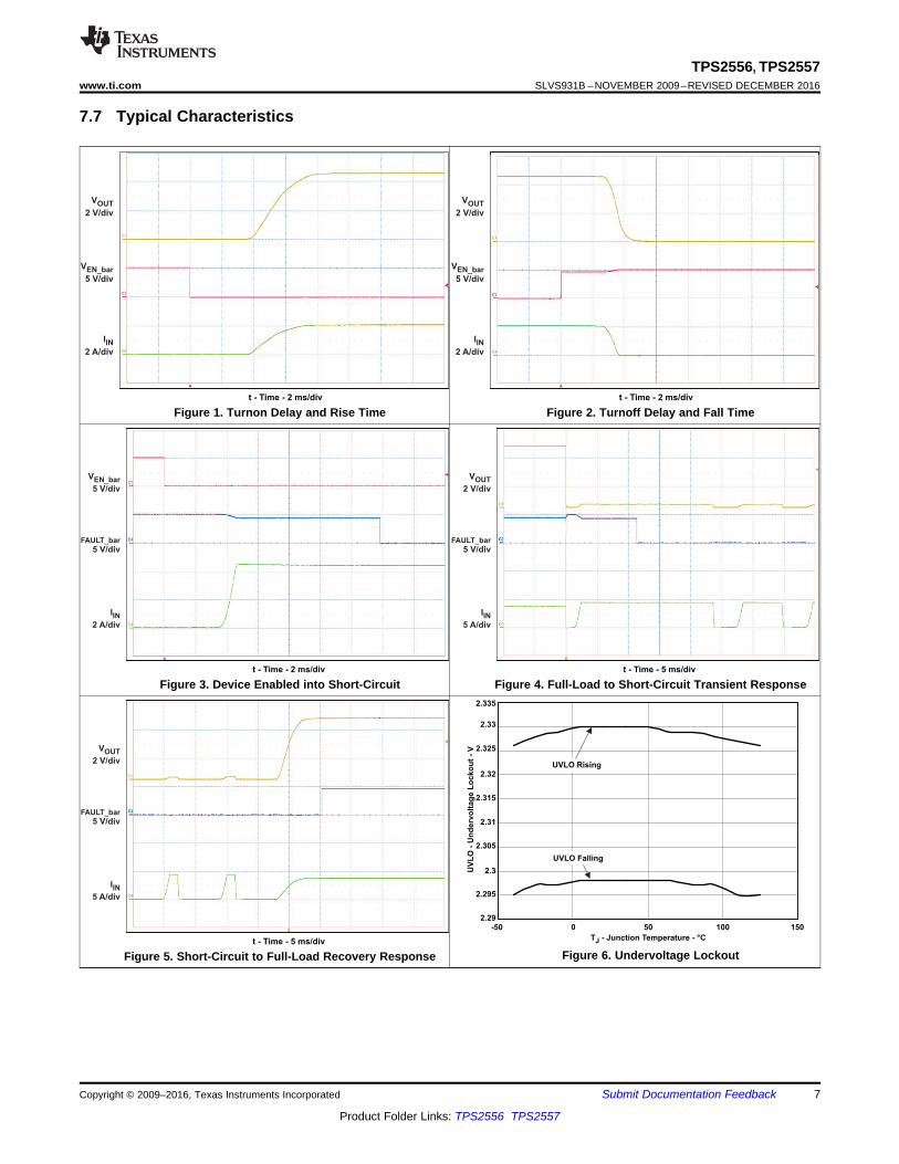
7.7 Typical Characteristics
Figure 1. Turnon Delay and Rise Time Figure 2. Turnoff Delay and Fall Time
Figure 3. Device Enabled into Short-Circuit Figure 4. Full-Load to Short-Circuit Transient Response
Figure 5. Short-Circuit to Full-Load Recovery Response Figure 6. Undervoltage Lockout
0
0.2
0.4
0.6
0.8
1.0
1.2
0 50 100 150 200
IDS
- S
tati
c D
rain
-So
urce C
urren
t -
A
V - V - mV/divIN OUT
T = 125°CA
T = 25°CA
T = -40°CA
R = 100 kILIM
W
0
0.2
0.4
0.6
0.8
1.0
1.2
1.4
1.6
1.8
2
0 20 40 60 80 100 120 140 160
IDS
- S
tati
c D
rain
-So
urce C
urren
t -
A
V - V - mV/divIN OUT
T = 125°CA
T = 25°CA
T = -40°CA
R = 61.9 kILIM
W
60
Input Voltage - V
2 3 4 5 6
IS
up
ply
Cu
rre
nt
vs
. V
IN E
na
ble
d -
AIN
μ
120
70
80
90
100
110
T = 125°CJ
T = 25°CJT = -40°CJ
7
R = 24.9kILIM Ω
0
r-
Sta
tic
Dra
in-S
ou
rce
On
-Sta
te R
es
ista
nc
e -
mD
S(o
n)
W
5
10
15
20
25
30
T - Junction Temperature - °CJ
-50 0 50 100 150
35
0
I-
Su
pp
ly C
urr
en
t, O
utp
ut
En
ab
led
-A
INm
120
20
40
60
80
100
T - Junction Temperature - °CJ
-50 0 50 100 150
R = 24.9 kILIM Ω
V = 6.5 VINV = 5 VIN
V = 3.3 VINV = 2.5 VIN
I-
Su
pp
ly C
urr
en
t, O
utp
ut
Dis
ab
led
- n
AIN
700
-100
0
100
200
300
400
500
600
T - Junction Temperature - °CJ
-50 0 50 100 150
V = 2.5 VIN
V = 6.5 VIN
8
TPS2556, TPS2557SLVS931B –NOVEMBER 2009–REVISED DECEMBER 2016 www.ti.com
Product Folder Links: TPS2556 TPS2557
Submit Documentation Feedback Copyright © 2009–2016, Texas Instruments Incorporated
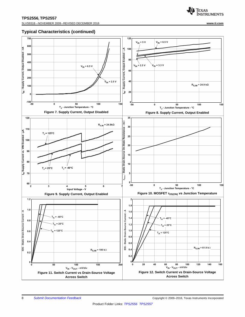
Typical Characteristics (continued)
Figure 7. Supply Current, Output Disabled Figure 8. Supply Current, Output Enabled
Figure 9. Supply Current, Output Enabled Figure 10. MOSFET rDS(ON) vs Junction Temperature
Figure 11. Switch Current vs Drain-Source VoltageAcross Switch
Figure 12. Switch Current vs Drain-Source VoltageAcross Switch
0
VIN-VOUT - mV
0 20 60 100 140
IDS
- S
tati
c D
rain
-So
urce C
urren
t -
A
3.0
0.5
1.0
1.5
2.0
2.5
T = 125°CJ
T = -40°CJ
T = 25°CJ
160
R = 24.9kILIM
Ω
40 80 120
5.0
4.5
4.0
3.5
9
TPS2556, TPS2557www.ti.com SLVS931B –NOVEMBER 2009–REVISED DECEMBER 2016
Product Folder Links: TPS2556 TPS2557
Submit Documentation FeedbackCopyright © 2009–2016, Texas Instruments Incorporated
Typical Characteristics (continued)
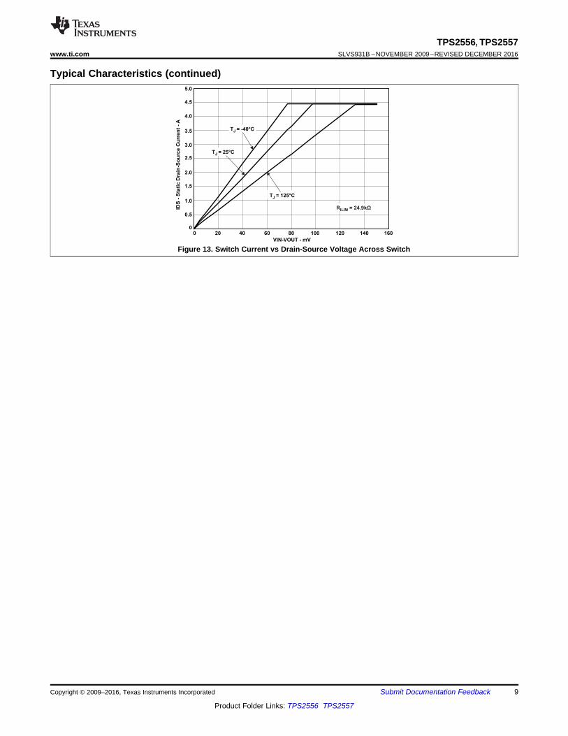
Figure 13. Switch Current vs Drain-Source Voltage Across Switch
VOUT
IOUT
IOS
DecreasingLoad Resistance
DecreasingLoad Resistance
tIOS
IOS
IOUT
RL CL
OUT
TEST CIRCUIT
tr tf
10%
90%
10%
90%VOUT
ton toff
10%
90%
50%50%
VEN
VOUT
VEN
VOUT
ton
toff
50% 50%
10%
90%
VOLTAGE WAVEFORMS
OUT
OUT
IN
IN
GND
FAULTILIM
EN24.9 kW
RFAULT
100 kW
Enable Signal
VIN = 5 V VOUT
TPS2556
0.1 uF
150 µF
Fault Signal
Power Pad
RLOAD
10
TPS2556, TPS2557SLVS931B –NOVEMBER 2009–REVISED DECEMBER 2016 www.ti.com
Product Folder Links: TPS2556 TPS2557
Submit Documentation Feedback Copyright © 2009–2016, Texas Instruments Incorporated
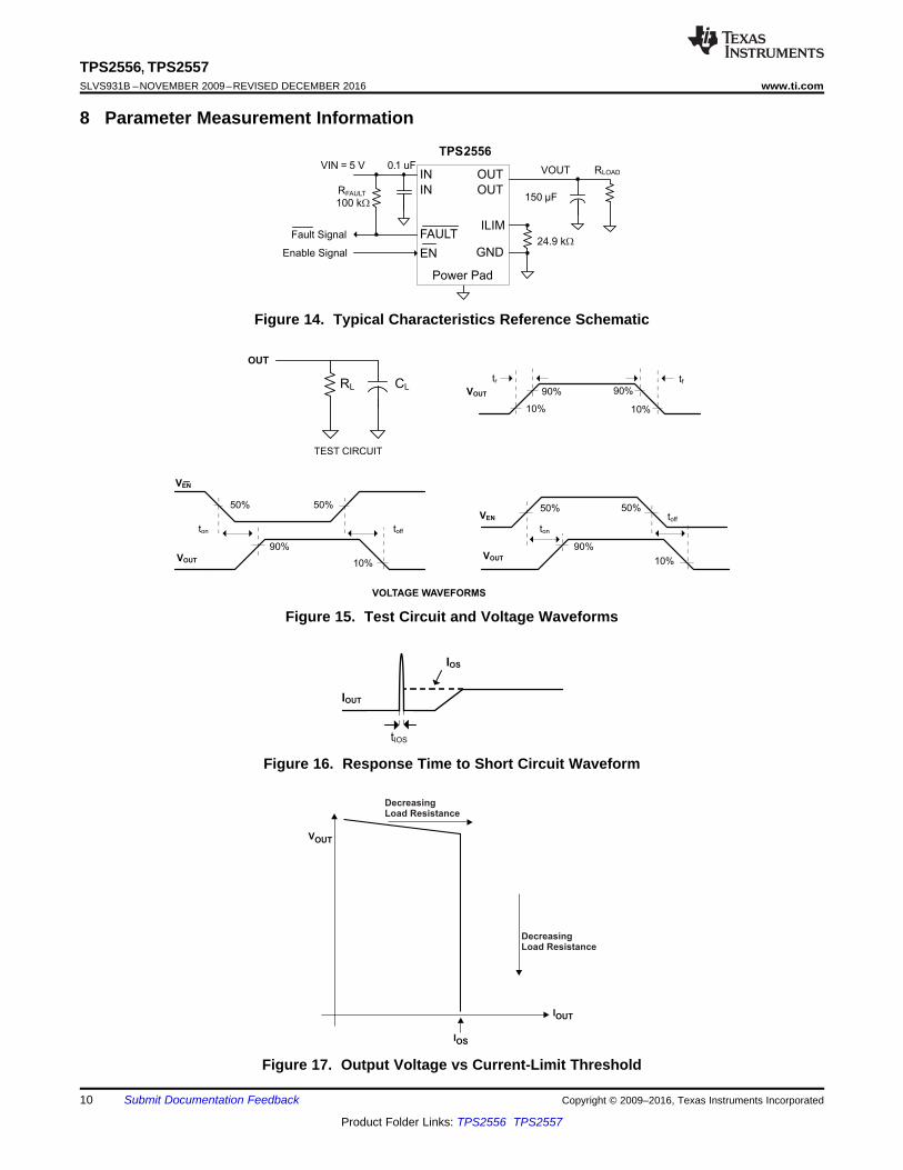
8 Parameter Measurement Information
Figure 14. Typical Characteristics Reference Schematic
Figure 15. Test Circuit and Voltage Waveforms
Figure 16. Response Time to Short Circuit Waveform
Figure 17. Output Voltage vs Current-Limit Threshold
ChargePump
Driver
UVLO
CurrentLimit
ThermalSense
8-ms Deglitch
IN
GND
EN
ILIM
OUT
FAULT
CS
CurrentSense
Copyright © 2016, Texas Instruments Incorporated
11
TPS2556, TPS2557www.ti.com SLVS931B –NOVEMBER 2009–REVISED DECEMBER 2016
Product Folder Links: TPS2556 TPS2557
Submit Documentation FeedbackCopyright © 2009–2016, Texas Instruments Incorporated
9 Detailed Description
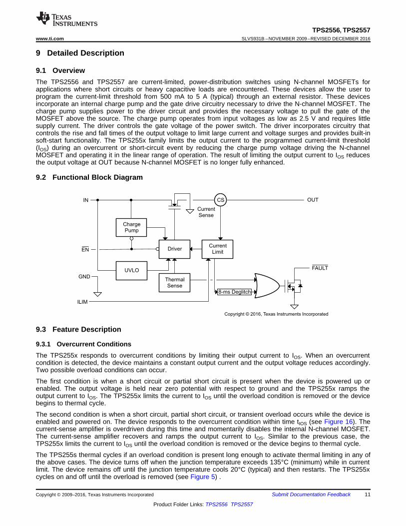
9.1 OverviewThe TPS2556 and TPS2557 are current-limited, power-distribution switches using N-channel MOSFETs forapplications where short circuits or heavy capacitive loads are encountered. These devices allow the user toprogram the current-limit threshold from 500 mA to 5 A (typical) through an external resistor. These devicesincorporate an internal charge pump and the gate drive circuitry necessary to drive the N-channel MOSFET. Thecharge pump supplies power to the driver circuit and provides the necessary voltage to pull the gate of theMOSFET above the source. The charge pump operates from input voltages as low as 2.5 V and requires littlesupply current. The driver controls the gate voltage of the power switch. The driver incorporates circuitry thatcontrols the rise and fall times of the output voltage to limit large current and voltage surges and provides built-insoft-start functionality. The TPS255x family limits the output current to the programmed current-limit threshold(IOS) during an overcurrent or short-circuit event by reducing the charge pump voltage driving the N-channelMOSFET and operating it in the linear range of operation. The result of limiting the output current to IOS reducesthe output voltage at OUT because N-channel MOSFET is no longer fully enhanced.
9.2 Functional Block Diagram
9.3 Feature Description
9.3.1 Overcurrent ConditionsThe TPS255x responds to overcurrent conditions by limiting their output current to IOS. When an overcurrentcondition is detected, the device maintains a constant output current and the output voltage reduces accordingly.Two possible overload conditions can occur.
The first condition is when a short circuit or partial short circuit is present when the device is powered up orenabled. The output voltage is held near zero potential with respect to ground and the TPS255x ramps theoutput current to IOS. The TPS255x limits the current to IOS until the overload condition is removed or the devicebegins to thermal cycle.
The second condition is when a short circuit, partial short circuit, or transient overload occurs while the device isenabled and powered on. The device responds to the overcurrent condition within time tIOS (see Figure 16). Thecurrent-sense amplifier is overdriven during this time and momentarily disables the internal N-channel MOSFET.The current-sense amplifier recovers and ramps the output current to IOS. Similar to the previous case, theTPS255x limits the current to IOS until the overload condition is removed or the device begins to thermal cycle.
The TPS255s thermal cycles if an overload condition is present long enough to activate thermal limiting in any ofthe above cases. The device turns off when the junction temperature exceeds 135°C (minimum) while in currentlimit. The device remains off until the junction temperature cools 20°C (typical) and then restarts. The TPS255xcycles on and off until the overload is removed (see Figure 5) .
12
TPS2556, TPS2557SLVS931B –NOVEMBER 2009–REVISED DECEMBER 2016 www.ti.com
Product Folder Links: TPS2556 TPS2557
Submit Documentation Feedback Copyright © 2009–2016, Texas Instruments Incorporated
Feature Description (continued)9.3.2 FAULT ResponseThe FAULT open-drain output is asserted (active low) during an overcurrent or overtemperature condition. TheTPS255s asserts the FAULT signal until the fault condition is removed and the device resumes normal operation.The TPS255s is designed to eliminate false FAULT reporting by using an internal delay deglitch circuit forovercurrent (9-ms typical) conditions without the need for external circuitry. This ensures that FAULT is notaccidentally asserted due to normal operation such as starting into a heavy capacitive load. The deglitch circuitrydelays entering and leaving current-limit induced fault conditions. The FAULTsignal is not deglitched when theMOSFET is disabled due to an overtemperature condition but is deglitched after the device has cooled andbegins to turn on. This unidirectional deglitch prevents FAULT oscillation during an overtemperature event.
9.3.3 Undervoltage Lockout (UVLO)The undervoltage lockout (UVLO) circuit disables the power switch until the input voltage reaches the UVLOturnon threshold. Built-in hysteresis prevents unwanted on and off cycling due to input voltage droop duringturnon.
9.3.4 Enable (EN OR EN)The logic enable controls the power switch and device supply current. The supply current is reduced to less than2-µA when a logic high is present on EN or when a logic low is present on EN. A logic low input on EN or a logichigh input on EN enables the driver, control circuits, and power switch. The enable input is compatible with bothTTL and CMOS logic levels.
9.3.5 Thermal SenseThe TPS255x self-protects by using two independent thermal sensing circuits that monitor the operatingtemperature of the power switch and disable operation if the temperature exceeds recommended operatingconditions. The TPS255x operates in constant-current mode during an overcurrent conditions, which increasesthe voltage drop across power switch. The power dissipation in the package is proportional to the voltage dropacross the power switch, which increases the junction temperature during an overcurrent condition. The firstthermal sensor (OTSD) turns off the power switch when the die temperature exceeds 135°C (minimum) and thepart is in current limit. Hysteresis is built into the thermal sensor, and the switch turns on after the device hascooled approximately 20°C.
The TPS255x also has a second ambient thermal sensor (OTSD2). The ambient thermal sensor turns off thepower switch when the die temperature exceeds 155°C (minimum) regardless of whether the power switch is incurrent limit and turns on the power switch after the device has cooled approximately 20°C. The TPS255xcontinues to cycle off and on until the fault is removed.
9.4 Device Functional ModesThere are no other functional modes.
OUT
OUT
IN
IN
GND
FAULTILIM
EN
R ILIM
R FAULT
100 kΩ
Control Signal
2.5V – 6.5V VOUT0.1 uF
CLOAD
Fault Signal
Power Pad
Copyright © 2016, Texas Instruments Incorporated
13
TPS2556, TPS2557www.ti.com SLVS931B –NOVEMBER 2009–REVISED DECEMBER 2016
Product Folder Links: TPS2556 TPS2557
Submit Documentation FeedbackCopyright © 2009–2016, Texas Instruments Incorporated
10 Application and Implementation
NOTEInformation in the following applications sections is not part of the TI componentspecification, and TI does not warrant its accuracy or completeness. TI’s customers areresponsible for determining suitability of components for their purposes. Customers shouldvalidate and test their design implementation to confirm system functionality.
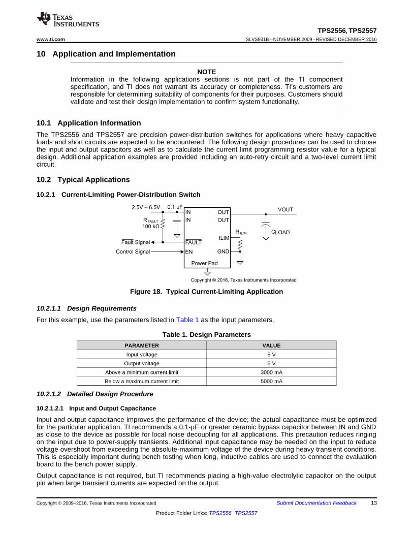
10.1 Application InformationThe TPS2556 and TPS2557 are precision power-distribution switches for applications where heavy capacitiveloads and short circuits are expected to be encountered. The following design procedures can be used to choosethe input and output capacitors as well as to calculate the current limit programming resistor value for a typicaldesign. Additional application examples are provided including an auto-retry circuit and a two-level current limitcircuit.
10.2 Typical Applications
10.2.1 Current-Limiting Power-Distribution Switch
Figure 18. Typical Current-Limiting Application
10.2.1.1 Design RequirementsFor this example, use the parameters listed in Table 1 as the input parameters.
Table 1. Design ParametersPARAMETER VALUEInput voltage 5 V
Output voltage 5 VAbove a minimum current limit 3000 mABelow a maximum current limit 5000 mA
10.2.1.2 Detailed Design Procedure
10.2.1.2.1 Input and Output Capacitance
Input and output capacitance improves the performance of the device; the actual capacitance must be optimizedfor the particular application. TI recommends a 0.1-µF or greater ceramic bypass capacitor between IN and GNDas close to the device as possible for local noise decoupling for all applications. This precaution reduces ringingon the input due to power-supply transients. Additional input capacitance may be needed on the input to reducevoltage overshoot from exceeding the absolute-maximum voltage of the device during heavy transient conditions.This is especially important during bench testing when long, inductive cables are used to connect the evaluationboard to the bench power supply.
Output capacitance is not required, but TI recommends placing a high-value electrolytic capacitor on the outputpin when large transient currents are expected on the output.
0
500
1000
1500
2000
2500
3000
3500
4000
4500
5000
5500
6000
20 30 40 50 60 70 80 90 100 110 120 130 140 150
R – Current Limit Resistor – kILIM
Ω
Cu
rren
t-L
imit
Th
resh
old
–m
A
IOS(min)
IOS(typ)IOS(max)
0.947ILIM
1.0028ILIM
1.0708ILIM
99038VOSmax R k
111704VOSnom R k
127981VOSmin R k
I (mA) =
I (mA) =
I (mA) =
W
W
W
14
TPS2556, TPS2557SLVS931B –NOVEMBER 2009–REVISED DECEMBER 2016 www.ti.com
Product Folder Links: TPS2556 TPS2557
Submit Documentation Feedback Copyright © 2009–2016, Texas Instruments Incorporated
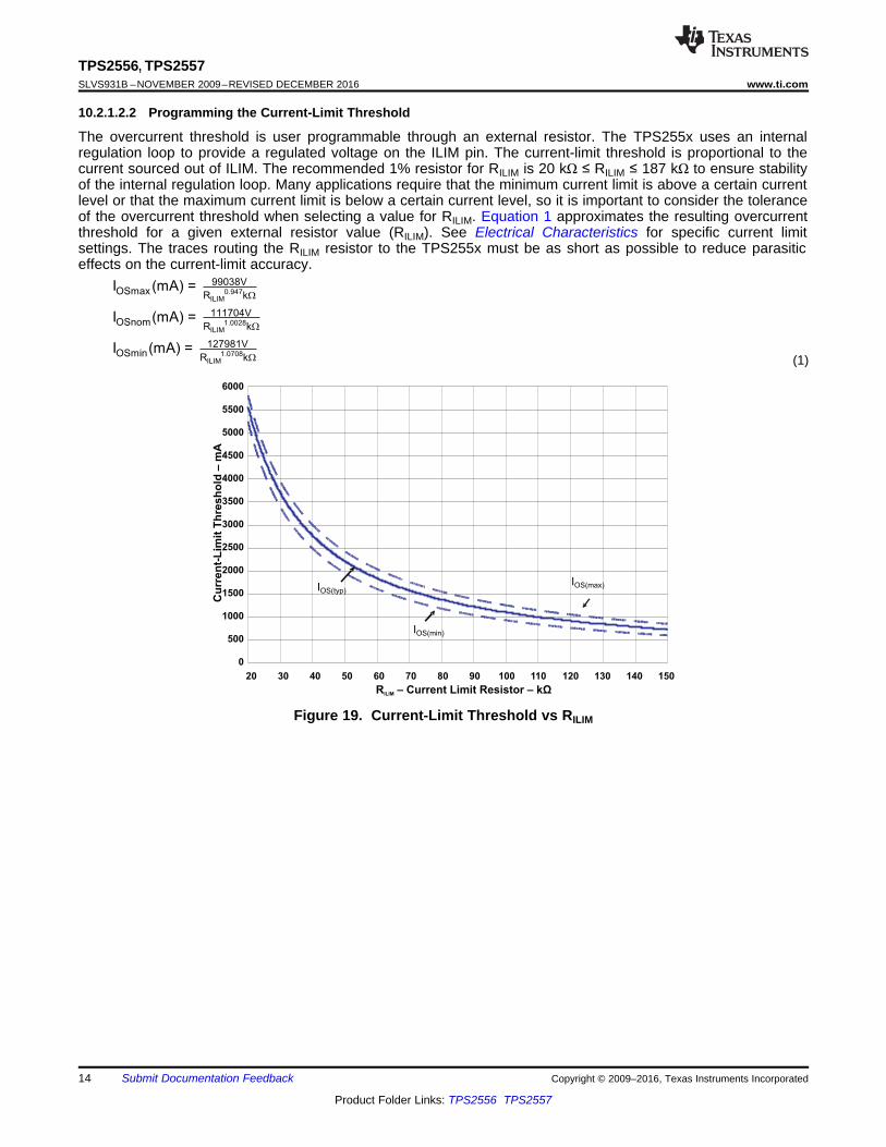
10.2.1.2.2 Programming the Current-Limit Threshold
The overcurrent threshold is user programmable through an external resistor. The TPS255x uses an internalregulation loop to provide a regulated voltage on the ILIM pin. The current-limit threshold is proportional to thecurrent sourced out of ILIM. The recommended 1% resistor for RILIM is 20 kΩ ≤ RILIM ≤ 187 kΩ to ensure stabilityof the internal regulation loop. Many applications require that the minimum current limit is above a certain currentlevel or that the maximum current limit is below a certain current level, so it is important to consider the toleranceof the overcurrent threshold when selecting a value for RILIM. Equation 1 approximates the resulting overcurrentthreshold for a given external resistor value (RILIM). See Electrical Characteristics for specific current limitsettings. The traces routing the RILIM resistor to the TPS255x must be as short as possible to reduce parasiticeffects on the current-limit accuracy.
(1)
Figure 19. Current-Limit Threshold vs RILIM
23.7
ILIM
OSmin 1.0708ILIM
OSmin 1.0708
OSmin
R (k ) = 23.7k
127981VI (mA) =
R k
127981VI (mA) =
k
I (mA) = 4316mA
W W
W
W
0.947ILIM
OSmax
99038VOSmax R k
1
0.947
ILIMOSmax
ILIM
I (mA) = 5000mA
I (mA) =
99038VR (k ) =
I mA
R (k ) = 23.4k
W
W
W W
æ ö÷ç ÷ç ÷ç ÷çè ø
ILIM
OSmax 0.947ILIM
OSmax 0.947
OSmax
R (k ) = 33.2k
99038VI (mA) =
R k
99038VI (mA) =
33.2 k
I (mA) = 3592mA
W W
W
W
1.0708ILIM
OSmin
127981VOSmin R k
1
1.0708
ILIMOSmin
ILIM
I (mA) = 3000mA
I (mA) =
127981VR (k ) =
I mA
R (k ) = 33.3k
W
W
W W
æ ö÷ç ÷ç ÷ç ÷çè ø
15
TPS2556, TPS2557www.ti.com SLVS931B –NOVEMBER 2009–REVISED DECEMBER 2016
Product Folder Links: TPS2556 TPS2557
Submit Documentation FeedbackCopyright © 2009–2016, Texas Instruments Incorporated
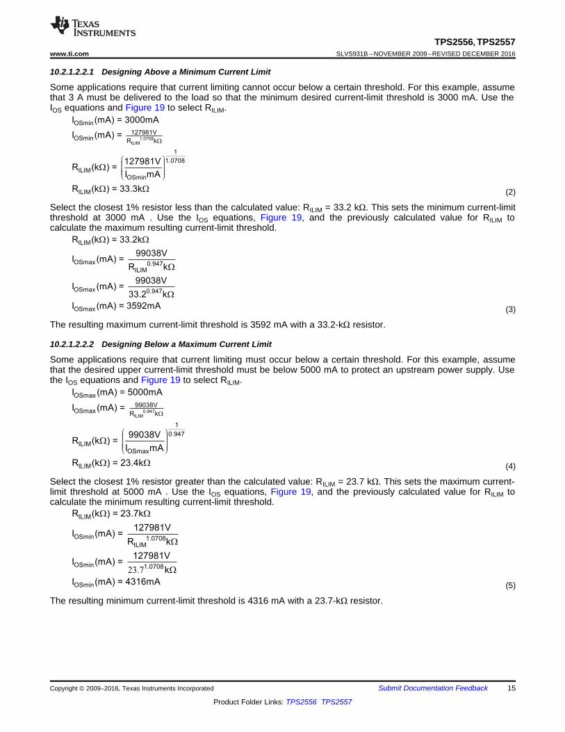
10.2.1.2.2.1 Designing Above a Minimum Current Limit
Some applications require that current limiting cannot occur below a certain threshold. For this example, assumethat 3 A must be delivered to the load so that the minimum desired current-limit threshold is 3000 mA. Use theIOS equations and Figure 19 to select RILIM.
(2)
Select the closest 1% resistor less than the calculated value: RILIM = 33.2 kΩ. This sets the minimum current-limitthreshold at 3000 mA . Use the IOS equations, Figure 19, and the previously calculated value for RILIM tocalculate the maximum resulting current-limit threshold.
(3)
The resulting maximum current-limit threshold is 3592 mA with a 33.2-kΩ resistor.
10.2.1.2.2.2 Designing Below a Maximum Current Limit
Some applications require that current limiting must occur below a certain threshold. For this example, assumethat the desired upper current-limit threshold must be below 5000 mA to protect an upstream power supply. Usethe IOS equations and Figure 19 to select RILIM.
(4)
Select the closest 1% resistor greater than the calculated value: RILIM = 23.7 kΩ. This sets the maximum current-limit threshold at 5000 mA . Use the IOS equations, Figure 19, and the previously calculated value for RILIM tocalculate the minimum resulting current-limit threshold.
(5)
The resulting minimum current-limit threshold is 4316 mA with a 23.7-kΩ resistor.
16
TPS2556, TPS2557SLVS931B –NOVEMBER 2009–REVISED DECEMBER 2016 www.ti.com
Product Folder Links: TPS2556 TPS2557
Submit Documentation Feedback Copyright © 2009–2016, Texas Instruments Incorporated
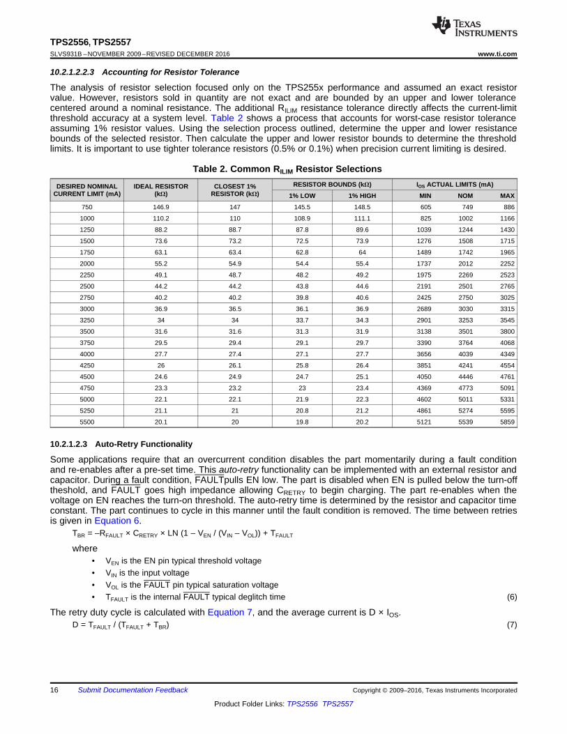
10.2.1.2.2.3 Accounting for Resistor Tolerance
The analysis of resistor selection focused only on the TPS255x performance and assumed an exact resistorvalue. However, resistors sold in quantity are not exact and are bounded by an upper and lower tolerancecentered around a nominal resistance. The additional RILIM resistance tolerance directly affects the current-limitthreshold accuracy at a system level. Table 2 shows a process that accounts for worst-case resistor toleranceassuming 1% resistor values. Using the selection process outlined, determine the upper and lower resistancebounds of the selected resistor. Then calculate the upper and lower resistor bounds to determine the thresholdlimits. It is important to use tighter tolerance resistors (0.5% or 0.1%) when precision current limiting is desired.
Table 2. Common RILIM Resistor Selections
DESIRED NOMINALCURRENT LIMIT (mA)
IDEAL RESISTOR(kΩ)
CLOSEST 1%RESISTOR (kΩ)
RESISTOR BOUNDS (kΩ) IOS ACTUAL LIMITS (mA)
1% LOW 1% HIGH MIN NOM MAX
750 146.9 147 145.5 148.5 605 749 886
1000 110.2 110 108.9 111.1 825 1002 1166
1250 88.2 88.7 87.8 89.6 1039 1244 1430
1500 73.6 73.2 72.5 73.9 1276 1508 1715
1750 63.1 63.4 62.8 64 1489 1742 1965
2000 55.2 54.9 54.4 55.4 1737 2012 2252
2250 49.1 48.7 48.2 49.2 1975 2269 2523
2500 44.2 44.2 43.8 44.6 2191 2501 2765
2750 40.2 40.2 39.8 40.6 2425 2750 3025
3000 36.9 36.5 36.1 36.9 2689 3030 3315
3250 34 34 33.7 34.3 2901 3253 3545
3500 31.6 31.6 31.3 31.9 3138 3501 3800
3750 29.5 29.4 29.1 29.7 3390 3764 4068
4000 27.7 27.4 27.1 27.7 3656 4039 4349
4250 26 26.1 25.8 26.4 3851 4241 4554
4500 24.6 24.9 24.7 25.1 4050 4446 4761
4750 23.3 23.2 23 23.4 4369 4773 5091
5000 22.1 22.1 21.9 22.3 4602 5011 5331
5250 21.1 21 20.8 21.2 4861 5274 5595
5500 20.1 20 19.8 20.2 5121 5539 5859
10.2.1.2.3 Auto-Retry Functionality
Some applications require that an overcurrent condition disables the part momentarily during a fault conditionand re-enables after a pre-set time. This auto-retry functionality can be implemented with an external resistor andcapacitor. During a fault condition, FAULTpulls EN low. The part is disabled when EN is pulled below the turn-offtheshold, and FAULT goes high impedance allowing CRETRY to begin charging. The part re-enables when thevoltage on EN reaches the turn-on threshold. The auto-retry time is determined by the resistor and capacitor timeconstant. The part continues to cycle in this manner until the fault condition is removed. The time between retriesis given in Equation 6.
TBR = –RFAULT × CRETRY × LN (1 – VEN / (VIN – VOL)) + TFAULT
where• VEN is the EN pin typical threshold voltage• VIN is the input voltage• VOL is the FAULT pin typical saturation voltage• TFAULT is the internal FAULT typical deglitch time (6)
The retry duty cycle is calculated with Equation 7, and the average current is D × IOS.D = TFAULT / (TFAULT + TBR) (7)
OUTIN
GND
FAULTILIM
EN
R ILIM
20 kW
RFAULT
100 kW
External Logic
Signal and Driver
TPS2557
0.1 uF
Power Pad
CLOAD RLOAD
CRETRY
0.22 µF
OutputInput
Copyright © 2016, Texas Instruments Incorporated
OUTIN
GND
FAULTILIM
EN
RILIM
20 kW
RFAULT
100 kW
Input
TPS2557
0.1 uF
Power Pad
CLOAD RLOAD
CRETRY
0.22 µF
Output
1 kW
Copyright © 2016, Texas Instruments Incorporated
17
TPS2556, TPS2557www.ti.com SLVS931B –NOVEMBER 2009–REVISED DECEMBER 2016
Product Folder Links: TPS2556 TPS2557
Submit Documentation FeedbackCopyright © 2009–2016, Texas Instruments Incorporated
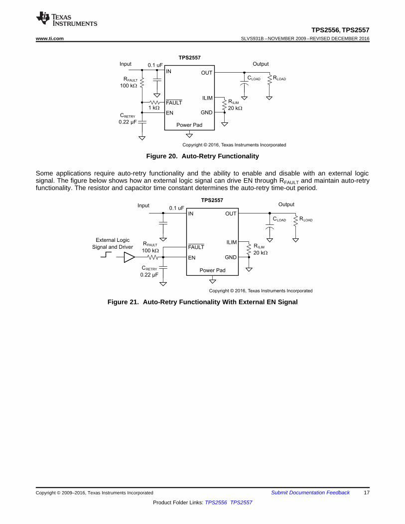
Figure 20. Auto-Retry Functionality
Some applications require auto-retry functionality and the ability to enable and disable with an external logicsignal. The figure below shows how an external logic signal can drive EN through RFAULT and maintain auto-retryfunctionality. The resistor and capacitor time constant determines the auto-retry time-out period.
Figure 21. Auto-Retry Functionality With External EN Signal
OUTIN
GND
FAULTILIM
EN
R1
187 kΩ
RFAULT
100 kΩ
Control Signal
InputTPS2556/57
0.1 uF
CLOAD
Fault Signal
Power Pad
Output
R2
22.1 kΩ
Current Limit
Control Signal
RLOAD
Q1
Copyright © 2016, Texas Instruments Incorporated
18
TPS2556, TPS2557SLVS931B –NOVEMBER 2009–REVISED DECEMBER 2016 www.ti.com
Product Folder Links: TPS2556 TPS2557
Submit Documentation Feedback Copyright © 2009–2016, Texas Instruments Incorporated
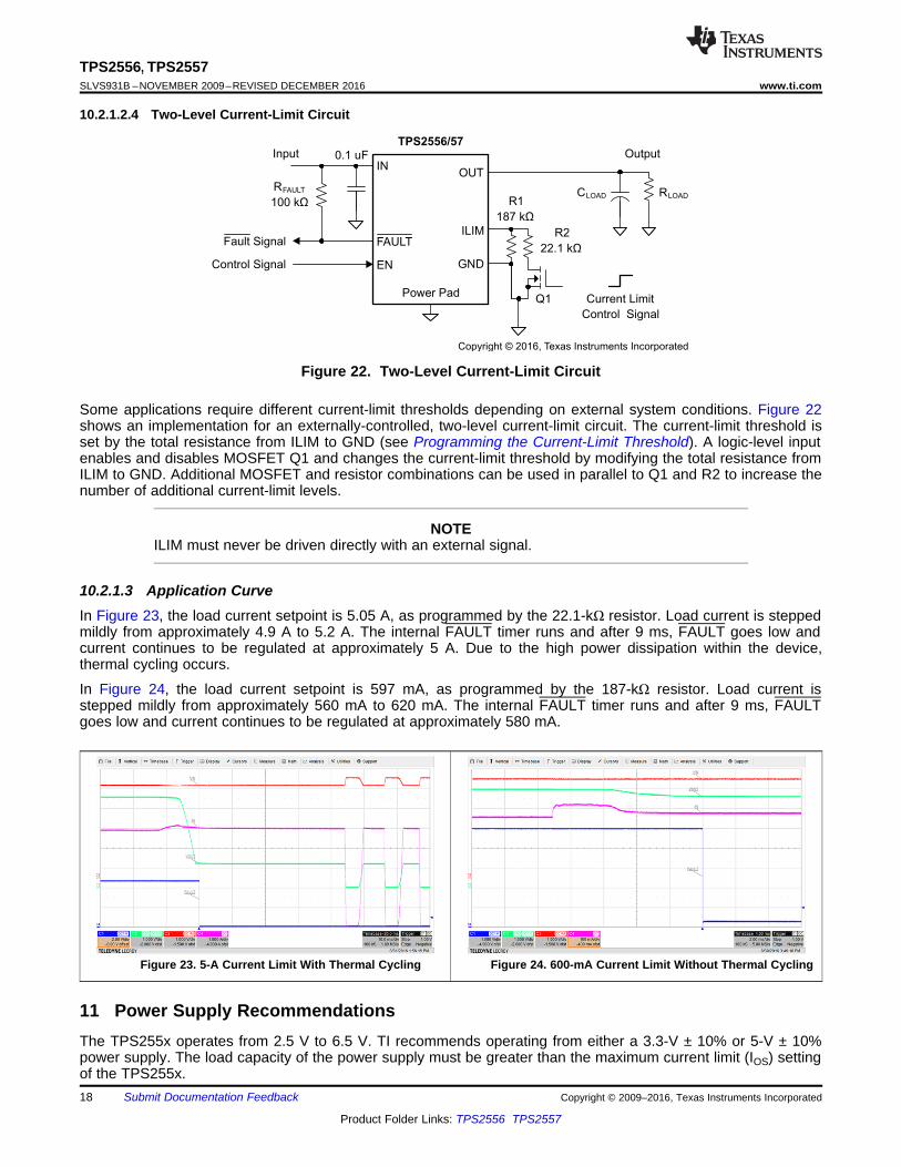
10.2.1.2.4 Two-Level Current-Limit Circuit
Figure 22. Two-Level Current-Limit Circuit
Some applications require different current-limit thresholds depending on external system conditions. Figure 22shows an implementation for an externally-controlled, two-level current-limit circuit. The current-limit threshold isset by the total resistance from ILIM to GND (see Programming the Current-Limit Threshold). A logic-level inputenables and disables MOSFET Q1 and changes the current-limit threshold by modifying the total resistance fromILIM to GND. Additional MOSFET and resistor combinations can be used in parallel to Q1 and R2 to increase thenumber of additional current-limit levels.
NOTEILIM must never be driven directly with an external signal.
10.2.1.3 Application CurveIn Figure 23, the load current setpoint is 5.05 A, as programmed by the 22.1-kΩ resistor. Load current is steppedmildly from approximately 4.9 A to 5.2 A. The internal FAULT timer runs and after 9 ms, FAULT goes low andcurrent continues to be regulated at approximately 5 A. Due to the high power dissipation within the device,thermal cycling occurs.
In Figure 24, the load current setpoint is 597 mA, as programmed by the 187-kΩ resistor. Load current isstepped mildly from approximately 560 mA to 620 mA. The internal FAULT timer runs and after 9 ms, FAULTgoes low and current continues to be regulated at approximately 580 mA.
Figure 23. 5-A Current Limit With Thermal Cycling Figure 24. 600-mA Current Limit Without Thermal Cycling
11 Power Supply RecommendationsThe TPS255x operates from 2.5 V to 6.5 V. TI recommends operating from either a 3.3-V ± 10% or 5-V ± 10%power supply. The load capacity of the power supply must be greater than the maximum current limit (IOS) settingof the TPS255x.
19
TPS2556, TPS2557www.ti.com SLVS931B –NOVEMBER 2009–REVISED DECEMBER 2016
Product Folder Links: TPS2556 TPS2557
Submit Documentation FeedbackCopyright © 2009–2016, Texas Instruments Incorporated
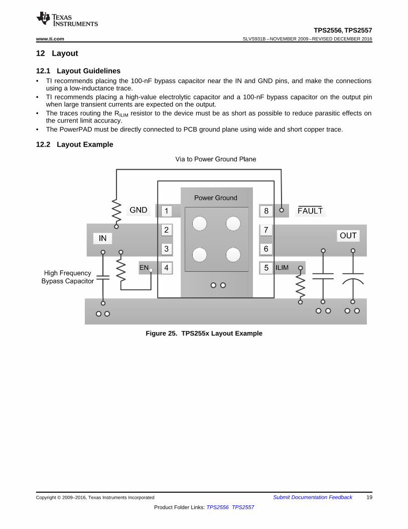
12 Layout
12.1 Layout Guidelines• TI recommends placing the 100-nF bypass capacitor near the IN and GND pins, and make the connections
using a low-inductance trace.• TI recommends placing a high-value electrolytic capacitor and a 100-nF bypass capacitor on the output pin
when large transient currents are expected on the output.• The traces routing the RILIM resistor to the device must be as short as possible to reduce parasitic effects on
the current limit accuracy.• The PowerPAD must be directly connected to PCB ground plane using wide and short copper trace.
12.2 Layout Example
Figure 25. TPS255x Layout Example
20
TPS2556, TPS2557SLVS931B –NOVEMBER 2009–REVISED DECEMBER 2016 www.ti.com
Product Folder Links: TPS2556 TPS2557
Submit Documentation Feedback Copyright © 2009–2016, Texas Instruments Incorporated
12.3 Thermal ConsiderationsThe low on-resistance of the N-channel MOSFET allows small surface-mount packages to pass large currents. Itis good design practice to estimate power dissipation and junction temperature. This analysis gives anapproximation for calculating junction temperature based on the power dissipation in the package. However,thermal analysis is strongly dependent on additional system level factors. Such factors include air flow, boardlayout, copper thickness and surface area, and proximity to other devices dissipating power. Good thermaldesign practice must include all system level factors in addition to individual component analysis.
Begin by determining the rDS(ON) of the N-channel MOSFET relative to the input voltage and operatingtemperature. As an initial estimate, use the highest operating ambient temperature of interest and read rDS(ON)from the typical characteristics graph. Using this value, the power dissipation can be calculated by Equation 8.
PD = rDS(ON) × IOUT2
where• PD = Total power dissipation (W)• rDS(ON) = Power switch on-resistance (Ω)• IOUT = Maximum current-limit threshold (A) (8)
Finally, calculate the junction temperature with Equation 9.TJ = PD × RθJA + TA
where• TA = Ambient temperature (°C)• RθJA = Thermal resistance (°C/W)• PD = Total power dissipation (W) (9)
Compare the calculated junction temperature with the initial estimate. If they are not within a few degrees, repeatthe calculation using the refined rDS(ON) from the previous calculation as the new estimate. Two or three iterationsare generally sufficient to achieve the desired result. The final junction temperature is highly dependent onthermal resistance, and thermal resistance is highly dependent on the individual package and board layout.
21
TPS2556, TPS2557www.ti.com SLVS931B –NOVEMBER 2009–REVISED DECEMBER 2016
Product Folder Links: TPS2556 TPS2557
Submit Documentation FeedbackCopyright © 2009–2016, Texas Instruments Incorporated
13 Device and Documentation Support
13.1 Related LinksThe table below lists quick access links. Categories include technical documents, support and communityresources, tools and software, and quick access to sample or buy.
Table 3. Related Links
PARTS PRODUCT FOLDER SAMPLE & BUY TECHNICALDOCUMENTS
TOOLS &SOFTWARE
SUPPORT &COMMUNITY
TPS2556 Click here Click here Click here Click here Click hereTPS2557 Click here Click here Click here Click here Click here
13.2 Receiving Notification of Documentation UpdatesTo receive notification of documentation updates, navigate to the device product folder on ti.com. In the upperright corner, click on Alert me to register and receive a weekly digest of any product information that haschanged. For change details, review the revision history included in any revised document.
13.3 Community ResourcesThe following links connect to TI community resources. Linked contents are provided "AS IS" by the respectivecontributors. They do not constitute TI specifications and do not necessarily reflect TI's views; see TI's Terms ofUse.
TI E2E™ Online Community TI's Engineer-to-Engineer (E2E) Community. Created to foster collaborationamong engineers. At e2e.ti.com, you can ask questions, share knowledge, explore ideas and helpsolve problems with fellow engineers.
Design Support TI's Design Support Quickly find helpful E2E forums along with design support tools andcontact information for technical support.
13.4 TrademarksPowerPAD, E2E are trademarks of Texas Instruments.All other trademarks are the property of their respective owners.
13.5 Electrostatic Discharge CautionThese devices have limited built-in ESD protection. The leads should be shorted together or the device placed in conductive foamduring storage or handling to prevent electrostatic damage to the MOS gates.
13.6 GlossarySLYZ022 — TI Glossary.
This glossary lists and explains terms, acronyms, and definitions.
14 Mechanical, Packaging, and Orderable InformationThe following pages include mechanical, packaging, and orderable information. This information is the mostcurrent data available for the designated devices. This data is subject to change without notice and revision ofthis document. For browser-based versions of this data sheet, refer to the left-hand navigation.
PACKAGE OPTION ADDENDUM
www.ti.com 26-Feb-2022
Addendum-Page 1
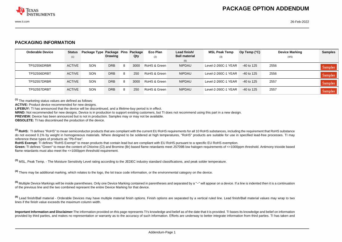
PACKAGING INFORMATION
Orderable Device Status(1)
Package Type PackageDrawing
Pins PackageQty
Eco Plan(2)
Lead finish/Ball material
(6)
MSL Peak Temp(3)
Op Temp (°C) Device Marking(4/5)
Samples
TPS2556DRBR ACTIVE SON DRB 8 3000 RoHS & Green NIPDAU Level-2-260C-1 YEAR -40 to 125 2556
TPS2556DRBT ACTIVE SON DRB 8 250 RoHS & Green NIPDAU Level-2-260C-1 YEAR -40 to 125 2556
TPS2557DRBR ACTIVE SON DRB 8 3000 RoHS & Green NIPDAU Level-2-260C-1 YEAR -40 to 125 2557
TPS2557DRBT ACTIVE SON DRB 8 250 RoHS & Green NIPDAU Level-2-260C-1 YEAR -40 to 125 2557
(1) The marketing status values are defined as follows:ACTIVE: Product device recommended for new designs.LIFEBUY: TI has announced that the device will be discontinued, and a lifetime-buy period is in effect.NRND: Not recommended for new designs. Device is in production to support existing customers, but TI does not recommend using this part in a new design.PREVIEW: Device has been announced but is not in production. Samples may or may not be available.OBSOLETE: TI has discontinued the production of the device.
(2) RoHS: TI defines "RoHS" to mean semiconductor products that are compliant with the current EU RoHS requirements for all 10 RoHS substances, including the requirement that RoHS substancedo not exceed 0.1% by weight in homogeneous materials. Where designed to be soldered at high temperatures, "RoHS" products are suitable for use in specified lead-free processes. TI mayreference these types of products as "Pb-Free".RoHS Exempt: TI defines "RoHS Exempt" to mean products that contain lead but are compliant with EU RoHS pursuant to a specific EU RoHS exemption.Green: TI defines "Green" to mean the content of Chlorine (Cl) and Bromine (Br) based flame retardants meet JS709B low halogen requirements of <=1000ppm threshold. Antimony trioxide basedflame retardants must also meet the <=1000ppm threshold requirement.
(3) MSL, Peak Temp. - The Moisture Sensitivity Level rating according to the JEDEC industry standard classifications, and peak solder temperature.
(4) There may be additional marking, which relates to the logo, the lot trace code information, or the environmental category on the device.
(5) Multiple Device Markings will be inside parentheses. Only one Device Marking contained in parentheses and separated by a "~" will appear on a device. If a line is indented then it is a continuationof the previous line and the two combined represent the entire Device Marking for that device.
(6) Lead finish/Ball material - Orderable Devices may have multiple material finish options. Finish options are separated by a vertical ruled line. Lead finish/Ball material values may wrap to twolines if the finish value exceeds the maximum column width.
Important Information and Disclaimer:The information provided on this page represents TI's knowledge and belief as of the date that it is provided. TI bases its knowledge and belief on informationprovided by third parties, and makes no representation or warranty as to the accuracy of such information. Efforts are underway to better integrate information from third parties. TI has taken and
PACKAGE OPTION ADDENDUM
www.ti.com 26-Feb-2022
Addendum-Page 2
continues to take reasonable steps to provide representative and accurate information but may not have conducted destructive testing or chemical analysis on incoming materials and chemicals.TI and TI suppliers consider certain information to be proprietary, and thus CAS numbers and other limited information may not be available for release.
In no event shall TI's liability arising out of such information exceed the total purchase price of the TI part(s) at issue in this document sold by TI to Customer on an annual basis.
OTHER QUALIFIED VERSIONS OF TPS2556, TPS2557 :
• Automotive : TPS2556-Q1, TPS2557-Q1
NOTE: Qualified Version Definitions:
• Automotive - Q100 devices qualified for high-reliability automotive applications targeting zero defects
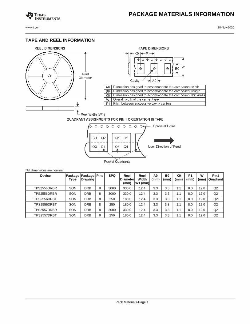
TAPE AND REEL INFORMATION
*All dimensions are nominal
Device PackageType
PackageDrawing
Pins SPQ ReelDiameter
(mm)
ReelWidth
W1 (mm)
A0(mm)
B0(mm)
K0(mm)
P1(mm)
W(mm)
Pin1Quadrant
TPS2556DRBR SON DRB 8 3000 330.0 12.4 3.3 3.3 1.1 8.0 12.0 Q2
TPS2556DRBR SON DRB 8 3000 330.0 12.4 3.3 3.3 1.1 8.0 12.0 Q2
TPS2556DRBT SON DRB 8 250 180.0 12.4 3.3 3.3 1.1 8.0 12.0 Q2
TPS2556DRBT SON DRB 8 250 180.0 12.4 3.3 3.3 1.1 8.0 12.0 Q2
TPS2557DRBR SON DRB 8 3000 330.0 12.4 3.3 3.3 1.1 8.0 12.0 Q2
TPS2557DRBT SON DRB 8 250 180.0 12.4 3.3 3.3 1.1 8.0 12.0 Q2
PACKAGE MATERIALS INFORMATION
www.ti.com 28-Nov-2020
Pack Materials-Page 1
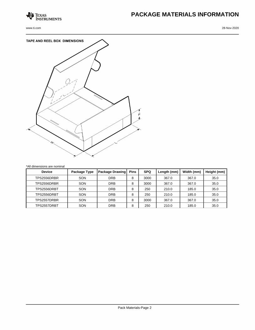
*All dimensions are nominal
Device Package Type Package Drawing Pins SPQ Length (mm) Width (mm) Height (mm)
TPS2556DRBR SON DRB 8 3000 367.0 367.0 35.0
TPS2556DRBR SON DRB 8 3000 367.0 367.0 35.0
TPS2556DRBT SON DRB 8 250 210.0 185.0 35.0
TPS2556DRBT SON DRB 8 250 210.0 185.0 35.0
TPS2557DRBR SON DRB 8 3000 367.0 367.0 35.0
TPS2557DRBT SON DRB 8 250 210.0 185.0 35.0
PACKAGE MATERIALS INFORMATION
www.ti.com 28-Nov-2020
Pack Materials-Page 2
www.ti.com
PACKAGE OUTLINE
C
8X 0.350.25
2.4 0.052X
1.95
1.65 0.05
6X 0.65
1 MAX
8X 0.50.3
0.050.00
A 3.12.9
B
3.12.9
(0.2) TYP
VSON - 1 mm max heightDRB0008BPLASTIC SMALL OUTLINE - NO LEAD
4218876/A 12/2017
PIN 1 INDEX AREA
SEATING PLANE
0.08 C
1
4 5
8
(OPTIONAL)PIN 1 ID 0.1 C A B
0.05 C
THERMAL PADEXPOSED
NOTES: 1. All linear dimensions are in millimeters. Any dimensions in parenthesis are for reference only. Dimensioning and tolerancing per ASME Y14.5M. 2. This drawing is subject to change without notice. 3. The package thermal pad must be soldered to the printed circuit board for thermal and mechanical performance.
SCALE 4.000
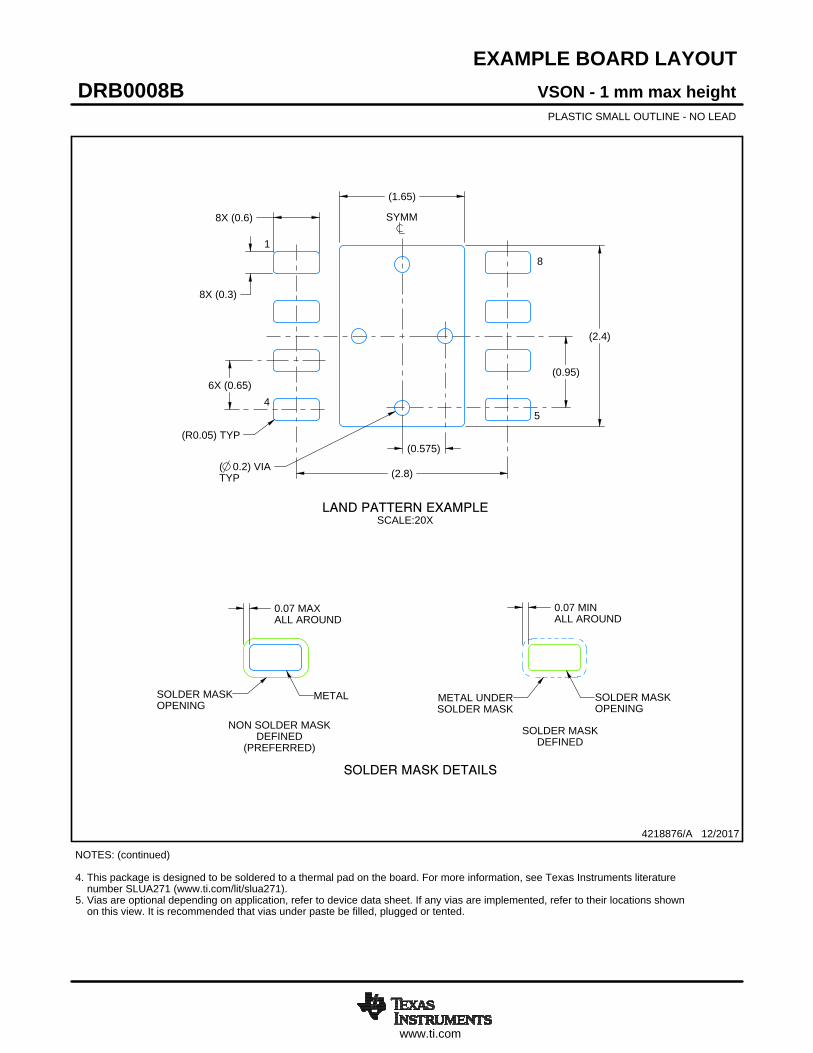
www.ti.com
EXAMPLE BOARD LAYOUT
0.07 MINALL AROUND
0.07 MAXALL AROUND
8X (0.3)
(2.4)
(2.8)
6X (0.65)
(1.65)
( 0.2) VIATYP
(0.575)
(0.95)
8X (0.6)
(R0.05) TYP
VSON - 1 mm max heightDRB0008BPLASTIC SMALL OUTLINE - NO LEAD
4218876/A 12/2017
SYMM
1
45
8
LAND PATTERN EXAMPLESCALE:20X
NOTES: (continued) 4. This package is designed to be soldered to a thermal pad on the board. For more information, see Texas Instruments literature number SLUA271 (www.ti.com/lit/slua271).5. Vias are optional depending on application, refer to device data sheet. If any vias are implemented, refer to their locations shown on this view. It is recommended that vias under paste be filled, plugged or tented.
SOLDER MASKOPENINGSOLDER MASK
METAL UNDER
SOLDER MASKDEFINED
METALSOLDER MASKOPENING
SOLDER MASK DETAILS
NON SOLDER MASKDEFINED
(PREFERRED)
www.ti.com
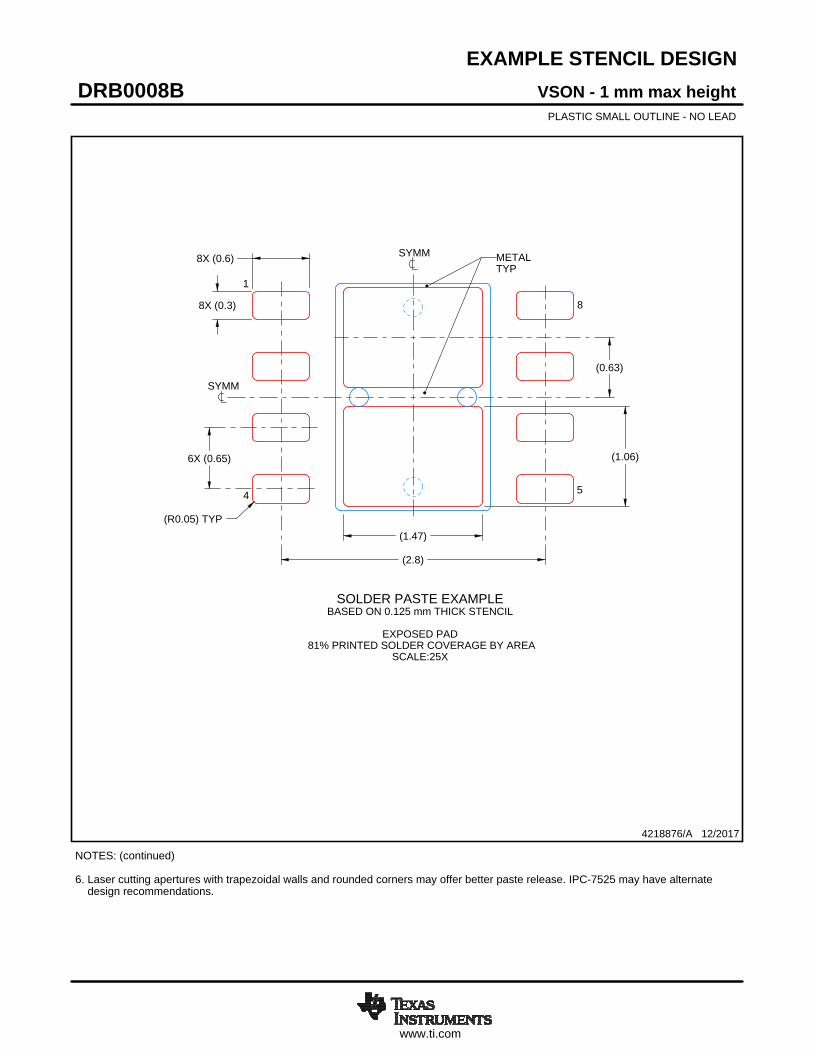
EXAMPLE STENCIL DESIGN
(R0.05) TYP
8X (0.3)
8X (0.6)
(1.47)
(1.06)
(2.8)
(0.63)
6X (0.65)
VSON - 1 mm max heightDRB0008BPLASTIC SMALL OUTLINE - NO LEAD
4218876/A 12/2017
NOTES: (continued) 6. Laser cutting apertures with trapezoidal walls and rounded corners may offer better paste release. IPC-7525 may have alternate design recommendations.
SOLDER PASTE EXAMPLEBASED ON 0.125 mm THICK STENCIL
EXPOSED PAD
81% PRINTED SOLDER COVERAGE BY AREASCALE:25X
SYMM
1
4 5
8
METALTYP
SYMM
IMPORTANT NOTICE AND DISCLAIMERTI PROVIDES TECHNICAL AND RELIABILITY DATA (INCLUDING DATA SHEETS), DESIGN RESOURCES (INCLUDING REFERENCE DESIGNS), APPLICATION OR OTHER DESIGN ADVICE, WEB TOOLS, SAFETY INFORMATION, AND OTHER RESOURCES “AS IS” AND WITH ALL FAULTS, AND DISCLAIMS ALL WARRANTIES, EXPRESS AND IMPLIED, INCLUDING WITHOUT LIMITATION ANY IMPLIED WARRANTIES OF MERCHANTABILITY, FITNESS FOR A PARTICULAR PURPOSE OR NON-INFRINGEMENT OF THIRD PARTY INTELLECTUAL PROPERTY RIGHTS.These resources are intended for skilled developers designing with TI products. You are solely responsible for (1) selecting the appropriate TI products for your application, (2) designing, validating and testing your application, and (3) ensuring your application meets applicable standards, and any other safety, security, regulatory or other requirements.These resources are subject to change without notice. TI grants you permission to use these resources only for development of an application that uses the TI products described in the resource. Other reproduction and display of these resources is prohibited. No license is granted to any other TI intellectual property right or to any third party intellectual property right. TI disclaims responsibility for, and you will fully indemnify TI and its representatives against, any claims, damages, costs, losses, and liabilities arising out of your use of these resources.TI’s products are provided subject to TI’s Terms of Sale or other applicable terms available either on ti.com or provided in conjunction with such TI products. TI’s provision of these resources does not expand or otherwise alter TI’s applicable warranties or warranty disclaimers for TI products.TI objects to and rejects any additional or different terms you may have proposed. IMPORTANT NOTICE
Mailing Address: Texas Instruments, Post Office Box 655303, Dallas, Texas 75265Copyright © 2022, Texas Instruments Incorporated