tps3700 high voltage (18v) window voltage detector with
TRANSCRIPT

R1
GND
1.8 V to 18 V
OUTA
OUTB
R2
R3
VMON
INA+
INB–
VDD
Device
RP2
RP1
0.1 µF
To a resetor enableinput ofthe system.
VIT+INA+
OU
TA
INB±
OU
TB
VIT+
Product
Folder
Order
Now
Technical
Documents
Tools &
Software
Support &Community
An IMPORTANT NOTICE at the end of this data sheet addresses availability, warranty, changes, use in safety-critical applications,intellectual property matters and other important disclaimers. PRODUCTION DATA.
TPS3700SBVS187G –FEBRUARY 2012–REVISED FEBRUARY 2019
TPS3700 High voltage (18V) window voltage detector with internal referencefor over and undervoltage monitoring
1
1 Features1• Wide supply voltage range: 1.8 V to 18 V• Adjustable threshold: down to 400 mV• High threshold accuracy:
– 1.0% over temperature– 0.25% (Typical)
• Low quiescent current: 5.5 µA (Typical)• Open-drain outputs for overvoltage and
undervoltage detection• Internal hysteresis: 5.5 mV (Typ)• Temperature range: –40°C to 125°C• Packages:
– SOT-6– 1.5-mm × 1.5-mm WSON-6
2 Applications• Industrial control systems• Automotive systems• Embedded computing modules• DSP, microcontroller, or microprocessor
applications• Notebook and desktop computers• Portable- and battery-powered products• FPGA and ASIC applications
3 DescriptionThe TPS3700 wide-supply window voltage detectoroperates over a 1.8-V to 18-V range. The device hastwo high-accuracy comparators with an internal 400-mV reference and two open-drain outputs rated to 18V for over- and undervoltage detection. The TPS3700can be used as a window voltage detector or as twoindependent voltage monitors; the monitored voltagecan be set with the use of external resistors.
OUTA is driven low when the voltage at INA+ dropsbelow (VITP – VHYS), and goes high when the voltagereturns above the respective threshold (VITP). OUTBis driven low when the voltage at INB– rises aboveVITP, and goes high when the voltage drops below therespective threshold (VITP – VHYS). Both comparatorsin the TPS3700 include built-in hysteresis for filteringto reject brief glitches, thereby ensuring stable outputoperation without false triggering.
The TPS3700 is available in a SOT-6 and a 1.5-mm× 1.5-mm WSON-6 package and is specified over thejunction temperature range of –40°C to 125°C.
Device Information(1)
PART NUMBER PACKAGE BODY SIZE (NOM)
TPS3700SOT (6) 2.90 mm × 1.60 mmWSON (6) 1.50 mm × 1.50 mm
(1) For all available packages, see the orderable addendum atthe end of the datasheet.
Simplified Schematic Output vs Input Thresholds and Hysteresis

2
TPS3700SBVS187G –FEBRUARY 2012–REVISED FEBRUARY 2019 www.ti.com
Product Folder Links: TPS3700
Submit Documentation Feedback Copyright © 2012–2019, Texas Instruments Incorporated
Table of Contents1 Features .................................................................. 12 Applications ........................................................... 13 Description ............................................................. 14 Revision History..................................................... 35 Pin Configuration and Functions ......................... 46 Specifications......................................................... 5
6.1 Absolute Maximum Ratings ...................................... 56.2 ESD Ratings.............................................................. 56.3 Recommended Operating Conditions....................... 56.4 Thermal Information .................................................. 56.5 Electrical Characteristics........................................... 66.6 Timing Requirements ................................................ 76.7 Switching Characteristics .......................................... 76.8 Typical Characteristics .............................................. 8
7 Detailed Description ............................................ 107.1 Overview ................................................................. 107.2 Functional Block Diagram ....................................... 107.3 Feature Description................................................. 10
7.4 Device Functional Modes........................................ 128 Application and Implementation ........................ 13
8.1 Application Information............................................ 138.2 Typical Application .................................................. 168.3 Do's and Don'ts....................................................... 18
9 Power-Supply Recommendations...................... 1910 Layout................................................................... 19
10.1 Layout Guidelines ................................................. 1910.2 Layout Example .................................................... 19
11 Device and Documentation Support ................. 2011.1 Device Support...................................................... 2011.2 Documentation Support ........................................ 2011.3 Receiving Notification of Documentation Updates 2011.4 Community Resources.......................................... 2011.5 Trademarks ........................................................... 2011.6 Electrostatic Discharge Caution............................ 2011.7 Glossary ................................................................ 21
12 Mechanical, Packaging, and OrderableInformation ........................................................... 21
3
TPS3700www.ti.com SBVS187G –FEBRUARY 2012–REVISED FEBRUARY 2019
Product Folder Links: TPS3700
Submit Documentation FeedbackCopyright © 2012–2019, Texas Instruments Incorporated
4 Revision HistoryNOTE: Page numbers for previous revisions may differ from page numbers in the current version.
Changes from Revision F (January 2018) to Revision G Page
• Changed comparator to voltage detector throughout datasheet ............................................................................................ 1
Changes from Revision E (February 2017) to Revision F Page
• Changed comparator to supervisor throughout datasheet .................................................................................................... 1
Changes from Revision D (January 2015) to Revision E Page
• Added maximum specification to Start-up delay parameter .................................................................................................. 6• Changed at least 150 µs to 450 µs (max) in footnote 2 of Electrical Characteristics table .................................................. 6
Changes from Revision C (May 2013) to Revision D Page
• Added ESD Ratings table, Feature Description section, Device Functional Modes, Application and Implementationsection, Power Supply Recommendations section, Layout section, Device and Documentation Support section, andMechanical, Packaging, and Orderable Information section ................................................................................................. 5
• Changed HBM maximum specification from 2 kV to 2.5 kV in ESD Ratings ......................................................................... 5• Changed Functional Block Diagram; added hysteresis symbol .......................................................................................... 10
Changes from Revision B (April 2012) to Revision C Page
• Changed Packages Features bullet ....................................................................................................................................... 1• Added SON-6 package option to Description section ............................................................................................................ 1• Added DSE pin out graphic to front page............................................................................................................................... 1• Added DSE pin out graphic .................................................................................................................................................... 4• Added DSE package to Thermal Information table ................................................................................................................ 5
Changes from Revision A (February 2012) to Revision B Page
• Moved to Production Data ...................................................................................................................................................... 1

1
2
3
6
5
4
OUTA
GND
INA+
OUTB
VDD
INB-
1
2
3
6
5
4
OUTB
VDD
INB-
OUTA
GND
INA+
4
TPS3700SBVS187G –FEBRUARY 2012–REVISED FEBRUARY 2019 www.ti.com
Product Folder Links: TPS3700
Submit Documentation Feedback Copyright © 2012–2019, Texas Instruments Incorporated
5 Pin Configuration and Functions
DDC PackageSOT-6
Top ViewDSE Package
WSON-6Top View
Pin FunctionsPIN
I/O DESCRIPTIONNAME DDC DSE
GND 2 5 — Ground
INA+ 3 4 IThis pin is connected to the voltage to be monitored with the use of an external resistordivider. When the voltage at this terminal drops below the threshold voltage (VITP –VHYS), OUTA is driven low.
INB– 4 3 IThis pin is connected to the voltage to be monitored with the use of an external resistordivider. When the voltage at this terminal exceeds the threshold voltage (VITP), OUTB isdriven low.
OUTA 1 6 OINA+ comparator open-drain output. OUTA is driven low when the voltage at thiscomparator is below (VITP – VHYS). The output goes high when the sense voltage returnsabove the respective threshold (VITP).
OUTB 6 1 OINB– comparator open-drain output. OUTB is driven low when the voltage at thiscomparator exceeds VITP. The output goes high when the sense voltage returns belowthe respective threshold (VITP – VHYS).
VDD 5 2 I Supply voltage input. Connect a 1.8-V to 18-V supply to VDD to power the device. Goodanalog design practice is to place a 0.1-µF ceramic capacitor close to this pin.

5
TPS3700www.ti.com SBVS187G –FEBRUARY 2012–REVISED FEBRUARY 2019
Product Folder Links: TPS3700
Submit Documentation FeedbackCopyright © 2012–2019, Texas Instruments Incorporated
(1) Stresses beyond those listed under Absolute Maximum Ratings may cause permanent damage to the device. These are stress ratingsonly, which do not imply functional operation of the device at these or any other conditions beyond those indicated under RecommendedOperating Conditions. Exposure to absolute-maximum-rated conditions for extended periods may affect device reliability.
(2) All voltages are with respect to network ground terminal.
6 Specifications
6.1 Absolute Maximum Ratingsover operating temperature range (unless otherwise noted) (1)
MIN MAX UNIT
Voltage (2)
VDD –0.3 20 VOUTA, OUTB –0.3 20 VINA+, INB– –0.3 7 V
Current Output terminal current 40 mAOperating junction temperature, TJ –40 125 °CStorage temperature, Tstg –65 150 °C
(1) JEDEC document JEP155 states that 500-V HBM allows safe manufacturing with a standard ESD control process.(2) JEDEC document JEP157 states that 250-V CDM allows safe manufacturing with a standard ESD control process.
6.2 ESD RatingsVALUE UNIT
V(ESD) Electrostatic dischargeHuman body model (HBM), per ANSI/ESDA/JEDEC JS-001, all pins (1) ±2500
VCharged device model (CDM), per JEDEC specification JESD22-C101,all pins (2) ±1000
6.3 Recommended Operating Conditionsover operating temperature range (unless otherwise noted)
MIN NOM MAX UNITVDD Supply voltage 1.8 18 VVI Input voltage INA+, INB– 0 6.5 VVO Output voltage OUTA, OUTB 0 18 V
(1) For more information about traditional and new thermal metrics, see the Semiconductor and IC Package Thermal Metrics applicationreport.
6.4 Thermal Information
THERMAL METRIC (1)TPS3700
UNITDDC (SOT) DSE (WSON)6 PINS 6 PINS
RθJA Junction-to-ambient thermal resistance 204.6 194.9 °C/WRθJC(top) Junction-to-case (top) thermal resistance 50.5 128.9 °C/WRθJB Junction-to-board thermal resistance 54.3 153.8 °C/WψJT Junction-to-top characterization parameter 0.8 11.9 °C/WψJB Junction-to-board characterization parameter 52.8 157.4 °C/WRθJC(bot) Junction-to-case (bottom) thermal resistance N/A N/A °C/W

6
TPS3700SBVS187G –FEBRUARY 2012–REVISED FEBRUARY 2019 www.ti.com
Product Folder Links: TPS3700
Submit Documentation Feedback Copyright © 2012–2019, Texas Instruments Incorporated
(1) The lowest supply voltage (VDD) at which output is active; tr(VDD) > 15 µs/V. Below V(POR), the output cannot be determined.(2) During power on, VDD must exceed 1.8 V for 450 µs (max) before the output is in a correct state.(3) When VDD falls below UVLO, OUTA is driven low and OUTB goes to high impedance. The outputs cannot be determined below V(POR).
6.5 Electrical CharacteristicsOver the operating temperature range of TJ = –40°C to 125°C, and 1.8 V < VDD < 18 V, unless otherwise noted.Typical values are at TJ = 25°C and VDD = 5 V.
PARAMETER TEST CONDITIONS MIN TYP MAX UNITVDD Supply voltage range 1.8 18 VV(POR) Power-on reset voltage (1) VOLmax = 0.2 V, I(OUTA/B) = 15 µA 0.8 V
VIT+ Positive-going input threshold voltageVDD = 1.8 V 396 400 404
mVVDD = 18 V 396 400 404
VIT– Negative-going input threshold voltageVDD = 1.8 V 387 394.5 400
mVVDD = 18 V 387 394.5 400
Vhys Hysteresis voltage (hys = VIT+ – VIT–) 5.5 12I(INA+) Input current (at the INA+ terminal) VDD = 1.8 V and 18 V, VI = 6.5 V –25 1 25 nAI(INB–) Input current (at the INB– terminal) VDD = 1.8 V and 18 V, VI = 0.1 V –15 1 15 nA
VOL Low-level output voltageVDD = 1.3 V, IO = 0.4 mA 250
mVVDD = 1.8 V, IO = 3 mA 250VDD = 5 V, IO = 5 mA 250
Ilkg(OD) Open-drain output leakage-currentVDD = 1.8 V and 18 V, VO = VDD 300
nAVDD = 1.8 V, VO = 18 V 300
IDD Supply current
VDD = 1.8 V, no load 5.5 11
µAVDD = 5 V 6 13VDD = 12 V 6 13VDD = 18 V 7 13
Start-up delay (2) 150 450 µsUVLO Undervoltage lockout (3) VDD falling 1.3 1.7 V

VDD
INA+
OUTA
INB–
OUTB
VIT+
Vhys
VIT+
Vhys
tPLH tPLH
tPLH
tPHL
tPHL
7
TPS3700www.ti.com SBVS187G –FEBRUARY 2012–REVISED FEBRUARY 2019
Product Folder Links: TPS3700
Submit Documentation FeedbackCopyright © 2012–2019, Texas Instruments Incorporated
(1) High-to-low and low-to-high refers to the transition at the input terminals (INA+ and INB–).
6.6 Timing Requirementsover operating temperature range (unless otherwise noted)
MIN NOM MAX UNIT
tPHL High-to-low propagation delay (1)VDD = 5 V, 10-mV input overdrive,RP = 10 kΩ, VOH = 0.9 × VDD, VOL = 400 mV,see Figure 1
18 µs
tPLH Low-to-high propagation delay (1)VDD = 5 V, 10-mV input overdrive,RP = 10 kΩ, VOH = 0.9 × VDD, VOL = 400 mV,see Figure 1
29 µs
6.7 Switching CharacteristicsOver operating temperature range (unless otherwise noted)
PARAMETER TEST CONDITIONS MIN TYP MAX UNIT
tr Output rise time VDD = 5 V, 10-mV input overdrive,RP = 10 kΩ, VO = (0.1 to 0.9) × VDD
2.2 µs
tf Output fall time VDD = 5 V, 10-mV input overdrive,RP = 10 kΩ, VO = (0.1 to 0.9) × VDD
0.22 µs
Figure 1. Timing Diagram

Positive-Going Input Threshold Overdrive (%)
Inp
ut
Pu
lse
Dura
tion
(µ
s)
2.5 4 5.5 7 8.5 10 11.5 13 14.5 160
2
4
6
8
10
12
14
16
18
20
D007
INA+INB–
Temperature (qC)
Low
-to-
Hig
h P
ropa
gatio
n D
elay
(µ
s)
-40 -25 -10 5 20 35 50 65 80 95 110 1258
10
12
14
16
18
20
22
24
26
28
30
D006
VDD = 1.8 V, INB� to OUTBVDD = 18 V, INB� to OUTBVDD = 1.8 V, INA+ to OUTAVDD = 18 V, INA+ to OUTA
Temperature (qC)
Hys
tere
sis
Vol
tage
(mV
)
-40 -25 -10 5 20 35 50 65 80 95 110 1253
4
5
6
7
8
9
D004
VDD = 1.8 VVDD = 5 VVDD = 12 VVDD = 18 V
Temperature (qC)
Low
-to-
Hig
h P
ropa
gatio
n D
elay
(µ
s)
-40 -25 -10 5 20 35 50 65 80 95 110 1259
11
13
15
17
19
21
23
25
27
29
31
D005
VDD = 1.8 V, INB� to OUTBVDD = 18 V, INB� to OUTBVDD = 1.8 V, INA+ to OUTAVDD = 18 V, INA+ to OUTA
Supply Voltage (V)
Sup
ply
Cur
rent
(µA
)
0 2 4 6 8 10 12 14 16 180
1
2
3
4
5
6
7
8
9
10
D001
�40qC0qC25qC85qC125qC
Temperature (qC)
Pos
itive
-Goi
ng In
put T
hres
hold
(mV
)
-40 -25 -10 5 20 35 50 65 80 95 110 125399
399.4
399.8
400.2
400.6
401
D003
VDD = 1.8 VVDD = 5 VVDD = 1.2 VVDD = 18 V
8
TPS3700SBVS187G –FEBRUARY 2012–REVISED FEBRUARY 2019 www.ti.com
Product Folder Links: TPS3700
Submit Documentation Feedback Copyright © 2012–2019, Texas Instruments Incorporated
6.8 Typical Characteristicsat TJ = 25°C and VDD = 5 V (unless otherwise noted)
Figure 2. Supply Current (IDD) vs Supply Voltage (VDD) Figure 3. Rising Input Threshold Voltage (VIT+) vsTemperature
Figure 4. Hysteresis (Vhys) vs Temperature Figure 5. Propagation Delay vs Temperature(High-to-Low Transition at the Inputs)
Figure 6. Propagation Delay vs Temperature(Low-to-High Transition at the Inputs)
INA+ = negative spike below VIT–INB– = positive spike above VIT+
Figure 7. Minimum Pulse Duration vsThreshold Overdrive Voltage

Output Sink Current (mA)
Low
-leve
l out
put v
olta
ge (
mV
)
0 5 10 15 20 25 30 35 400
250
500
750
1000
1250
1500
1750
2000
D012
VDD = 1.8 VVDD = 5 VVDD = 18 V
Output Sink Current (mA)
Low
-leve
l out
put v
olta
ge (
mV
)
0 5 10 15 20 25 30 35 400
250
500
750
1000
1250
1500
1750
2000
D013
VDD = 1.8 VVDD = 5 VVDD = 18 V
Output Sink Current (mA)
Low
-Lev
el O
utpu
t Vol
tage
(mV
)
0 5 10 15 20 25 30 35 400
250
500
750
1000
1250
1500
1750
2000
D010
VDD = 1.8 VVDD = 5 VVDD = 18 V
Output Sink Current (mA)
Low
-Lev
el O
utpu
t Vol
tage
(m
V)
0 5 10 15 20 25 30 35 400
250
500
750
1000
1250
1500
1750
2000
D011
VDD = 1.8 VVDD = 5 VVDD = 18 V
Output Sink Current (mA)
Low
-Lev
el O
utpu
t Vol
tage
(mV
)
0 5 10 15 20 25 30 35 400
250
500
750
1000
1250
1500
1750
2000
D009
VDD = 1.8 VVDD = 5 VVDD = 18 V
Output Sink Current (mA)
Sup
ply
Cur
rent
(µA
)
0 4 8 12 16 20 24 28 32 36 401
2
3
4
5
6
7
8
9
10
11
D008
�40qC0qC25qC85qC125qC
9
TPS3700www.ti.com SBVS187G –FEBRUARY 2012–REVISED FEBRUARY 2019
Product Folder Links: TPS3700
Submit Documentation FeedbackCopyright © 2012–2019, Texas Instruments Incorporated
Typical Characteristics (continued)at TJ = 25°C and VDD = 5 V (unless otherwise noted)
Figure 8. Supply Current (IDD) vsOutput Sink Current
Figure 9. Output Voltage Low (VOL) vsOutput Sink Current (–40°C)
Figure 10. Output Voltage Low (VOL) vsOutput Sink Current (0°C)
Figure 11. Output Voltage Low (VOL) vsOutput Sink Current (25°C)
Figure 12. Output Voltage Low (VOL) vsOutput Sink Current (85°C)
Figure 13. Output Voltage Low (VOL) vsOutput Sink Current (125°C)

INA+
GND
INB–
VDD
OUTA
OUTB
Reference
10
TPS3700SBVS187G –FEBRUARY 2012–REVISED FEBRUARY 2019 www.ti.com
Product Folder Links: TPS3700
Submit Documentation Feedback Copyright © 2012–2019, Texas Instruments Incorporated
7 Detailed Description
7.1 OverviewThe TPS3700 device combines two voltage detectors for overvoltage and undervoltage detection. The TPS3700device is a wide-supply voltage range (1.8 V to 18 V) device with a high-accuracy rising input threshold of400 mV (1% over temperature) and built-in hysteresis. The outputs are also rated to 18 V and can sink up to40 mA.
The TPS3700 device is designed to assert the output signals, as shown in Table 1. Each input terminal can beset to monitor any voltage above 0.4 V using an external resistor divider network. With the use of two inputterminals of different polarities, the TPS3700 device forms a window voltage detector. Broad voltage thresholdscan be supported that allow the device to be used in a wide array of applications.
Table 1. TPS3700 Truth TableCONDITION OUTPUT STATUSINA+ > VIT+ OUTA high Output A not assertedINA+ < VIT– OUTA low Output A assertedINB– > VIT+ OUTB low Output B assertedINB– < VIT– OUTB high Output B not asserted
7.2 Functional Block Diagram
7.3 Feature Description
7.3.1 Inputs (INA+, INB–)The TPS3700 device is a voltage detector that combines two comparators. Each comparator has one externalinput (inverting and noninverting); the other input is connected to the internal reference. The comparator risingthreshold is designed and trimmed to be equal to the reference voltage (400 mV). Both comparators also have abuilt-in falling hysteresis that makes the device less sensitive to supply rail noise and ensures stable operation.
The INA+ and INB- inputs can swing from ground to 6.5 V, regardless of the device supply voltage used.Although not required in most cases, good analog design practice is to place a 1-nF to 10-nF bypass capacitor atthe comparator input for extremely noisy applications to reduce sensitivity to transients and layout parasitics.
For comparator A, the corresponding output (OUTA) is driven to logic low when the input INA+ voltage dropsbelow (VIT+ – Vhys). When the voltage exceeds VIT+, the output (OUTA) goes to a high-impedance state; seeFigure 1.
R
(2.21 M )1
W
GND
1.8 V to 18 V
OUTA
OUTB
R2
(13.7 k )W
R3
(69.8 k )W
VMON
INA+
INB–
VDD
Device
RP1
(50 k )W
VoltageRegulator
IN
EN
VO
OUT
VMONUV OV
OU
T
11
TPS3700www.ti.com SBVS187G –FEBRUARY 2012–REVISED FEBRUARY 2019
Product Folder Links: TPS3700
Submit Documentation FeedbackCopyright © 2012–2019, Texas Instruments Incorporated
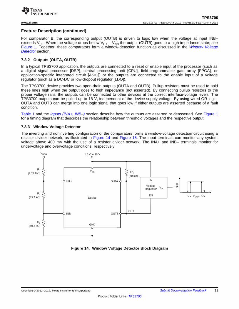
Feature Description (continued)For comparator B, the corresponding output (OUTB) is driven to logic low when the voltage at input INB–exceeds VIT+. When the voltage drops below VIT+ – Vhys the output (OUTB) goes to a high-impedance state; seeFigure 1. Together, these comparators form a window-detection function as discussed in the Window VoltageDetector section.
7.3.2 Outputs (OUTA, OUTB)In a typical TPS3700 application, the outputs are connected to a reset or enable input of the processor (such asa digital signal processor [DSP], central processing unit [CPU], field-programmable gate array [FPGA], orapplication-specific integrated circuit [ASIC]) or the outputs are connected to the enable input of a voltageregulator (such as a DC-DC or low-dropout regulator [LDO]).
The TPS3700 device provides two open-drain outputs (OUTA and OUTB). Pullup resistors must be used to holdthese lines high when the output goes to high impedance (not asserted). By connecting pullup resistors to theproper voltage rails, the outputs can be connected to other devices at the correct interface-voltage levels. TheTPS3700 outputs can be pulled up to 18 V, independent of the device supply voltage. By using wired-OR logic,OUTA and OUTB can merge into one logic signal that goes low if either outputs are asserted because of a faultcondition.
Table 1 and the Inputs (INA+, INB–) section describe how the outputs are asserted or deasserted. See Figure 1for a timing diagram that describes the relationship between threshold voltages and the respective output.
7.3.3 Window Voltage DetectorThe inverting and noninverting configuration of the comparators forms a window-voltage detection circuit using aresistor divider network, as illustrated in Figure 14 and Figure 15. The input terminals can monitor any systemvoltage above 400 mV with the use of a resistor divider network. The INA+ and INB– terminals monitor forundervoltage and overvoltage conditions, respectively.
Figure 14. Window Voltage Detector Block Diagram
OvervoltageLimit
UndervoltageLimit
VMON
OUTB
OUTA
12
TPS3700SBVS187G –FEBRUARY 2012–REVISED FEBRUARY 2019 www.ti.com
Product Folder Links: TPS3700
Submit Documentation Feedback Copyright © 2012–2019, Texas Instruments Incorporated
Feature Description (continued)
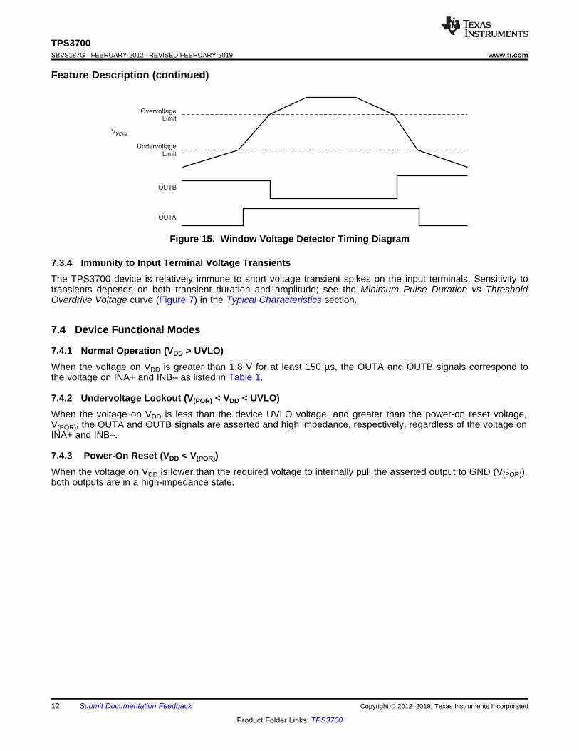
Figure 15. Window Voltage Detector Timing Diagram
7.3.4 Immunity to Input Terminal Voltage TransientsThe TPS3700 device is relatively immune to short voltage transient spikes on the input terminals. Sensitivity totransients depends on both transient duration and amplitude; see the Minimum Pulse Duration vs ThresholdOverdrive Voltage curve (Figure 7) in the Typical Characteristics section.
7.4 Device Functional Modes
7.4.1 Normal Operation (VDD > UVLO)When the voltage on VDD is greater than 1.8 V for at least 150 µs, the OUTA and OUTB signals correspond tothe voltage on INA+ and INB– as listed in Table 1.
7.4.2 Undervoltage Lockout (V(POR) < VDD < UVLO)When the voltage on VDD is less than the device UVLO voltage, and greater than the power-on reset voltage,V(POR), the OUTA and OUTB signals are asserted and high impedance, respectively, regardless of the voltage onINA+ and INB–.
7.4.3 Power-On Reset (VDD < V(POR))When the voltage on VDD is lower than the required voltage to internally pull the asserted output to GND (V(POR)),both outputs are in a high-impedance state.

GND
1.8 V to 18 V
OUTA
OUTB
INA+
INB–
VDD
Device
V
(Up To 18 V)PULLUP
To a reset or enable inputof the system.
13
TPS3700www.ti.com SBVS187G –FEBRUARY 2012–REVISED FEBRUARY 2019
Product Folder Links: TPS3700
Submit Documentation FeedbackCopyright © 2012–2019, Texas Instruments Incorporated
8 Application and Implementation
NOTEInformation in the following applications sections is not part of the TI componentspecification, and TI does not warrant its accuracy or completeness. TI’s customers areresponsible for determining suitability of components for their purposes. Customers shouldvalidate and test their design implementation to confirm system functionality.
8.1 Application InformationThe TPS3700 device is a wide-supply window voltage detector that operates over a VDD range of 1.8 V to 18 V.The device has two high-accuracy comparators with an internal 400-mV reference and two open-drain outputsrated to 18 V for overvoltage and undervoltage detection. The device can be used either as a window voltagedetector or as two independent voltage monitors. The monitored voltages are set with the use of externalresistors.
8.1.1 VPULLUP to a Voltage Other Than VDD
The outputs are often tied to VDD through a resistor. However, some applications may require the outputs to bepulled up to a higher or lower voltage than VDD to correctly interface with the reset and enable terminals of otherdevices.
Figure 16. Interfacing to Voltages Other Than VDD

R1
(2.61 M )W
GND
1.8 V to 18 V
OUTA
OUTB
R2
(8.06 k )W
R3
(40.2 k )W
VMON
(26.4 V to 21.7 V)
INA+
INB–
VDD
Device
To a reset or enable inputof the system.
GND
1.8 V to 18 V
OUTA
OUTB
INA+
INB–
VDD
DeviceTo a reset or enable inputof the system.
14
TPS3700SBVS187G –FEBRUARY 2012–REVISED FEBRUARY 2019 www.ti.com
Product Folder Links: TPS3700
Submit Documentation Feedback Copyright © 2012–2019, Texas Instruments Incorporated
Application Information (continued)8.1.2 Monitoring VDD
Many applications monitor the same rail that is powering VDD. In these applications the resistor divider is simplyconnected to the VDD rail.
Figure 17. Monitoring the Same Voltage as VDD
8.1.3 Monitoring a Voltage Other Than VDD
Some applications monitor rails other than the one that is powering VDD. In these types of applications theresistor divider used to set the desired thresholds is connected to the rail that is being monitored.
NOTE: The inputs can monitor a voltage higher than VDDmax with the use of an external resistor divider network.
Figure 18. Monitoring a Voltage Other Than VDD
GND
1.8 V to 18 V
OUTA
OUTB
INA+
INB–
VDD
Device
5 V
12 V
VIT+INA+
OU
TA
VIT+INB–
OU
TB
To a reset or enableinput of the system.
15
TPS3700www.ti.com SBVS187G –FEBRUARY 2012–REVISED FEBRUARY 2019
Product Folder Links: TPS3700
Submit Documentation FeedbackCopyright © 2012–2019, Texas Instruments Incorporated
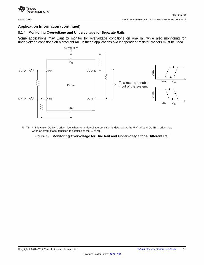
Application Information (continued)8.1.4 Monitoring Overvoltage and Undervoltage for Separate RailsSome applications may want to monitor for overvoltage conditions on one rail while also monitoring forundervoltage conditions on a different rail. In these applications two independent resistor dividers must be used.
NOTE: In this case, OUTA is driven low when an undervoltage condition is detected at the 5-V rail and OUTB is driven lowwhen an overvoltage condition is detected at the 12-V rail.
Figure 19. Monitoring Overvoltage for One Rail and Undervoltage for a Different Rail

R =3
RT
VMON(OV)
´ VIT+
5
3
1
6
24
R449.9 k
R549.9 k
VPULLUP
OUTA
OUTB
GND
VDD
INA+
INB±
VDD
R12.21 M
R213.7 k
R369.8 k
C10.1 µF U1
TPS3700DDC
16
TPS3700SBVS187G –FEBRUARY 2012–REVISED FEBRUARY 2019 www.ti.com
Product Folder Links: TPS3700
Submit Documentation Feedback Copyright © 2012–2019, Texas Instruments Incorporated
8.2 Typical ApplicationThe TPS3700 device is a wide-supply window voltage detector that operates over a VDD range of 1.8 to 18 V.The monitored voltages are set with the use of external resistors, so the device can be used either as a windowvoltage detector or as two independent overvoltage and undervoltage monitors.
Figure 20. Typical Application Schematic
8.2.1 Design RequirementsFor this design example, use the values summarized in Table 2 as the input parameters.
Table 2. Design ParametersPARAMETER DESIGN REQUIREMENT DESIGN RESULT
Monitored voltage 12-V nominal rail with maximum rising andfalling thresholds of ±10%
VMON(UV)= 10.99 V (8.33%) ±2.94%,VMON(OV)= 13.14 V (8.33%) ±2.94%
8.2.2 Detailed Design Procedure
8.2.2.1 Resistor Divider SelectionUse Equation 1 through Equation 4 to calculate the resistor divider values and target threshold voltages.
RT = R1 + R2 + R3 (1)
Select a value for RT such that the current through the divider is approximately 100 times higher than the inputcurrent at the INA+ and INB– terminals. The resistors can have high values to minimize current consumption asa result of low-input bias current without adding significant error to the resistive divider. See the application noteOptimizing Resistor Dividers at a Comparator Input (SLVA450) for details on sizing input resistors.
Use Equation 2 to calculate the value of R3.
where:
VMON(OV) is the target voltage at which an overvoltage condition is detected (2)

V
IPU
O
(V V )HI PU-
Ilkg(OD)
³ ³RPU
% ACC = % TOL(V ) + 2IT+(INB) ´
V
VIT+(INB)
MON(OV)
1- ´ ´% TOL = 1% + 2R 1-
0.413.2
´ 1% = 2.94%
R =2
RT
VMON(UV)
- R3´ (V VIT+ hys- )
R =2
RT
V (no UV)MON
´ VIT+ - R3
17
TPS3700www.ti.com SBVS187G –FEBRUARY 2012–REVISED FEBRUARY 2019
Product Folder Links: TPS3700
Submit Documentation FeedbackCopyright © 2012–2019, Texas Instruments Incorporated
Use Equation 3 or Equation 4 to calculate the value of R2.
where:
VMON(no UV) is the target voltage at which an undervoltage condition is removed as VMON rises (3)
where:VMON(UV) is the target voltage at which an undervoltage condition is detected (4)
The worst-case tolerance can be calculated by referring to Equation 13 in application report SLVA450,Optimizing Resistor Dividers at a Comparator Input (available for download at www.ti.com). An example of therising threshold error, VMON(OV), is given in Equation 5.
(5)
8.2.2.2 Pullup Resistor SelectionTo ensure proper voltage levels, the pullup resistor value is selected by ensuring that the pullup voltage dividedby the resistor does not exceed the sink-current capability of the device. This confirmation is calculated byverifying that the pullup voltage minus the output-leakage current (Ilkg(OD)) multiplied by the resistor is greater thedesired logic-high voltage. These values are specified in the Electrical Characteristics table.
Use Equation 6 to calculate the value of the pullup resistor.
(6)
8.2.2.3 Input Supply CapacitorAlthough an input capacitor is not required for stability, connecting a 0.1-μF low equivalent series resistance(ESR) capacitor across the VDD terminal and GND terminal is good analog design practice. A higher-valuecapacitor may be necessary if large, fast rise-time load transients are anticipated, or if the device is not locatedclose to the power source.
8.2.2.4 Input CapacitorsAlthough not required in most cases, for extremely noisy applications, placing a 1-nF to 10-nF bypass capacitorfrom the comparator inputs (INA+, INB–) to the GND terminal is good analog design practice. This capacitorplacement reduces device sensitivity to transients.
Time (100 µs/div) G013
OUTA
OUTB
VDD
C1(2 V/div)
C3(2 V/div)
C2(2 V/div)
Time (100 µs/div) G014
OUTA
OUTB
VDD
C1(2 V/div)
C3(2 V/div)
C2(2 V/div)
18
TPS3700SBVS187G –FEBRUARY 2012–REVISED FEBRUARY 2019 www.ti.com
Product Folder Links: TPS3700
Submit Documentation Feedback Copyright © 2012–2019, Texas Instruments Incorporated
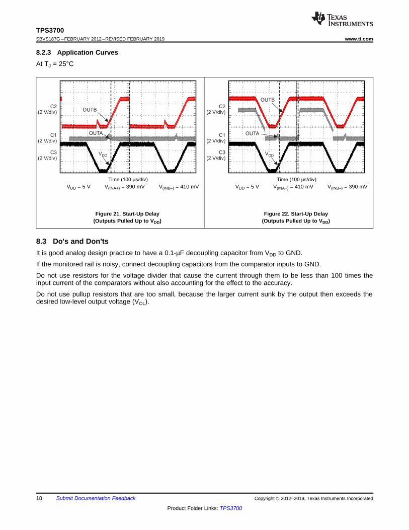
8.2.3 Application CurvesAt TJ = 25°C
VDD = 5 V V(INA+) = 390 mV V(INB–) = 410 mV
Figure 21. Start-Up Delay(Outputs Pulled Up to VDD)
VDD = 5 V V(INA+) = 410 mV V(INB–) = 390 mV
Figure 22. Start-Up Delay(Outputs Pulled Up to VDD)
8.3 Do's and Don'tsIt is good analog design practice to have a 0.1-µF decoupling capacitor from VDD to GND.
If the monitored rail is noisy, connect decoupling capacitors from the comparator inputs to GND.
Do not use resistors for the voltage divider that cause the current through them to be less than 100 times theinput current of the comparators without also accounting for the effect to the accuracy.
Do not use pullup resistors that are too small, because the larger current sunk by the output then exceeds thedesired low-level output voltage (VOL).

VP
ULLU
PV
PU
LLU
PV
PU
LLU
P
19
TPS3700www.ti.com SBVS187G –FEBRUARY 2012–REVISED FEBRUARY 2019
Product Folder Links: TPS3700
Submit Documentation FeedbackCopyright © 2012–2019, Texas Instruments Incorporated
9 Power-Supply RecommendationsThese devices are designed to operate from an input voltage supply range between 1.8 V and 18 V.
10 Layout
10.1 Layout GuidelinesPlacing a 0.1-µF capacitor close to the VDD terminal to reduce the input impedance to the device is good analogdesign practice. The pullup resistors can be separated if separate logic functions are needed (as shown inFigure 23) or both resistors can be tied to a single pullup resistor if a logical AND function is desired.
10.2 Layout Example
Figure 23. TPS3700 Layout Schematic
20
TPS3700SBVS187G –FEBRUARY 2012–REVISED FEBRUARY 2019 www.ti.com
Product Folder Links: TPS3700
Submit Documentation Feedback Copyright © 2012–2019, Texas Instruments Incorporated
11 Device and Documentation Support
11.1 Device Support
11.1.1 Development Support
11.1.1.1 Evaluation ModulesTwo evaluation modules (EVMs) are available to assist in the initial circuit performance evaluation using theTPS3700. The TPS3700EVM-114 evaluation module and the TPS3700EVM-202 evaluation module (and therelated user's guides) can be requested at the Texas Instruments website through the TPS3700 product folder orpurchased directly from the TI eStore.
11.1.2 Device Nomenclature
Table 3. Device NomenclaturePRODUCT DESCRIPTION
TPS3700yyyz yyy is package designatorz is package quantity
11.2 Documentation Support
11.2.1 Related DocumentationFor related documentation, see the following:• Using the TPS3700 as a negative rail over- and undervoltage detector• Optimizing resistor dividers at a comparator input• TPS3700EVM-114 Evaluation module user guide• TPS3700EVM-202 Evaluation module user guide
11.3 Receiving Notification of Documentation UpdatesTo receive notification of documentation updates, navigate to the device product folder on ti.com. In the upperright corner, click on Alert me to register and receive a weekly digest of any product information that haschanged. For change details, review the revision history included in any revised document.
11.4 Community ResourcesThe following links connect to TI community resources. Linked contents are provided "AS IS" by the respectivecontributors. They do not constitute TI specifications and do not necessarily reflect TI's views; see TI's Terms ofUse.
TI E2E™ Online Community TI's Engineer-to-Engineer (E2E) Community. Created to foster collaborationamong engineers. At e2e.ti.com, you can ask questions, share knowledge, explore ideas and helpsolve problems with fellow engineers.
Design Support TI's Design Support Quickly find helpful E2E forums along with design support tools andcontact information for technical support.
11.5 TrademarksE2E is a trademark of Texas Instruments.All other trademarks are the property of their respective owners.
11.6 Electrostatic Discharge CautionThis integrated circuit can be damaged by ESD. Texas Instruments recommends that all integrated circuits be handled withappropriate precautions. Failure to observe proper handling and installation procedures can cause damage.
ESD damage can range from subtle performance degradation to complete device failure. Precision integrated circuits may be moresusceptible to damage because very small parametric changes could cause the device not to meet its published specifications.

21
TPS3700www.ti.com SBVS187G –FEBRUARY 2012–REVISED FEBRUARY 2019
Product Folder Links: TPS3700
Submit Documentation FeedbackCopyright © 2012–2019, Texas Instruments Incorporated
11.7 GlossarySLYZ022 — TI Glossary.
This glossary lists and explains terms, acronyms, and definitions.
12 Mechanical, Packaging, and Orderable InformationThe following pages include mechanical, packaging, and orderable information. This information is the mostcurrent data available for the designated devices. This data is subject to change without notice and revision ofthis document. For browser-based versions of this data sheet, refer to the left-hand navigation.
Figure 0. UNDEFINEDFigure 0. UNDEFINED

22
TPS3700SBVS187G –FEBRUARY 2012–REVISED FEBRUARY 2019 www.ti.com
Product Folder Links: TPS3700
Submit Documentation Feedback Copyright © 2012–2019, Texas Instruments Incorporated
Figure 0. UNDEFINED
Figure 0. UNDEFINED

PACKAGE OPTION ADDENDUM
www.ti.com 10-Dec-2020
Addendum-Page 1
PACKAGING INFORMATION
Orderable Device Status(1)
Package Type PackageDrawing
Pins PackageQty
Eco Plan(2)
Lead finish/Ball material
(6)
MSL Peak Temp(3)
Op Temp (°C) Device Marking(4/5)
Samples
TPS3700DDCR ACTIVE SOT-23-THIN DDC 6 3000 RoHS & Green NIPDAU Level-2-260C-1 YEAR -40 to 125 PXVQ
TPS3700DDCR2 ACTIVE SOT-23-THIN DDC 6 3000 RoHS & Green NIPDAU Level-2-260C-1 YEAR -40 to 125 PB4Q
TPS3700DDCT ACTIVE SOT-23-THIN DDC 6 250 RoHS & Green NIPDAU Level-2-260C-1 YEAR -40 to 125 PXVQ
TPS3700DSER ACTIVE WSON DSE 6 3000 RoHS & Green NIPDAU Level-1-260C-UNLIM -40 to 125 (7I, BE)
TPS3700DSET ACTIVE WSON DSE 6 250 RoHS & Green NIPDAU Level-1-260C-UNLIM -40 to 125 (7I, BE)
(1) The marketing status values are defined as follows:ACTIVE: Product device recommended for new designs.LIFEBUY: TI has announced that the device will be discontinued, and a lifetime-buy period is in effect.NRND: Not recommended for new designs. Device is in production to support existing customers, but TI does not recommend using this part in a new design.PREVIEW: Device has been announced but is not in production. Samples may or may not be available.OBSOLETE: TI has discontinued the production of the device.
(2) RoHS: TI defines "RoHS" to mean semiconductor products that are compliant with the current EU RoHS requirements for all 10 RoHS substances, including the requirement that RoHS substancedo not exceed 0.1% by weight in homogeneous materials. Where designed to be soldered at high temperatures, "RoHS" products are suitable for use in specified lead-free processes. TI mayreference these types of products as "Pb-Free".RoHS Exempt: TI defines "RoHS Exempt" to mean products that contain lead but are compliant with EU RoHS pursuant to a specific EU RoHS exemption.Green: TI defines "Green" to mean the content of Chlorine (Cl) and Bromine (Br) based flame retardants meet JS709B low halogen requirements of <=1000ppm threshold. Antimony trioxide basedflame retardants must also meet the <=1000ppm threshold requirement.
(3) MSL, Peak Temp. - The Moisture Sensitivity Level rating according to the JEDEC industry standard classifications, and peak solder temperature.
(4) There may be additional marking, which relates to the logo, the lot trace code information, or the environmental category on the device.
(5) Multiple Device Markings will be inside parentheses. Only one Device Marking contained in parentheses and separated by a "~" will appear on a device. If a line is indented then it is a continuationof the previous line and the two combined represent the entire Device Marking for that device.
(6) Lead finish/Ball material - Orderable Devices may have multiple material finish options. Finish options are separated by a vertical ruled line. Lead finish/Ball material values may wrap to twolines if the finish value exceeds the maximum column width.

PACKAGE OPTION ADDENDUM
www.ti.com 10-Dec-2020
Addendum-Page 2
Important Information and Disclaimer:The information provided on this page represents TI's knowledge and belief as of the date that it is provided. TI bases its knowledge and belief on informationprovided by third parties, and makes no representation or warranty as to the accuracy of such information. Efforts are underway to better integrate information from third parties. TI has taken andcontinues to take reasonable steps to provide representative and accurate information but may not have conducted destructive testing or chemical analysis on incoming materials and chemicals.TI and TI suppliers consider certain information to be proprietary, and thus CAS numbers and other limited information may not be available for release.
In no event shall TI's liability arising out of such information exceed the total purchase price of the TI part(s) at issue in this document sold by TI to Customer on an annual basis.
OTHER QUALIFIED VERSIONS OF TPS3700 :
• Automotive: TPS3700-Q1
NOTE: Qualified Version Definitions:
• Automotive - Q100 devices qualified for high-reliability automotive applications targeting zero defects

TAPE AND REEL INFORMATION
*All dimensions are nominal
Device PackageType
PackageDrawing
Pins SPQ ReelDiameter
(mm)
ReelWidth
W1 (mm)
A0(mm)
B0(mm)
K0(mm)
P1(mm)
W(mm)
Pin1Quadrant
TPS3700DDCR SOT-23-THIN
DDC 6 3000 179.0 8.4 3.2 3.2 1.4 4.0 8.0 Q3
TPS3700DDCR2 SOT-23-THIN
DDC 6 3000 179.0 8.4 3.2 3.2 1.4 4.0 8.0 Q2
TPS3700DDCT SOT-23-THIN
DDC 6 250 179.0 8.4 3.2 3.2 1.4 4.0 8.0 Q3
TPS3700DSER WSON DSE 6 3000 178.0 8.4 1.7 1.7 0.95 4.0 8.0 Q2
TPS3700DSET WSON DSE 6 250 178.0 8.4 1.7 1.7 0.95 4.0 8.0 Q2
PACKAGE MATERIALS INFORMATION
www.ti.com 7-Jan-2021
Pack Materials-Page 1

*All dimensions are nominal
Device Package Type Package Drawing Pins SPQ Length (mm) Width (mm) Height (mm)
TPS3700DDCR SOT-23-THIN DDC 6 3000 213.0 191.0 35.0
TPS3700DDCR2 SOT-23-THIN DDC 6 3000 213.0 191.0 35.0
TPS3700DDCT SOT-23-THIN DDC 6 250 213.0 191.0 35.0
TPS3700DSER WSON DSE 6 3000 205.0 200.0 33.0
TPS3700DSET WSON DSE 6 250 205.0 200.0 33.0
PACKAGE MATERIALS INFORMATION
www.ti.com 7-Jan-2021
Pack Materials-Page 2

IMPORTANT NOTICE AND DISCLAIMERTI PROVIDES TECHNICAL AND RELIABILITY DATA (INCLUDING DATASHEETS), DESIGN RESOURCES (INCLUDING REFERENCEDESIGNS), APPLICATION OR OTHER DESIGN ADVICE, WEB TOOLS, SAFETY INFORMATION, AND OTHER RESOURCES “AS IS”AND WITH ALL FAULTS, AND DISCLAIMS ALL WARRANTIES, EXPRESS AND IMPLIED, INCLUDING WITHOUT LIMITATION ANYIMPLIED WARRANTIES OF MERCHANTABILITY, FITNESS FOR A PARTICULAR PURPOSE OR NON-INFRINGEMENT OF THIRDPARTY INTELLECTUAL PROPERTY RIGHTS.These resources are intended for skilled developers designing with TI products. You are solely responsible for (1) selecting the appropriateTI products for your application, (2) designing, validating and testing your application, and (3) ensuring your application meets applicablestandards, and any other safety, security, or other requirements. These resources are subject to change without notice. TI grants youpermission to use these resources only for development of an application that uses the TI products described in the resource. Otherreproduction and display of these resources is prohibited. No license is granted to any other TI intellectual property right or to any third partyintellectual property right. TI disclaims responsibility for, and you will fully indemnify TI and its representatives against, any claims, damages,costs, losses, and liabilities arising out of your use of these resources.TI’s products are provided subject to TI’s Terms of Sale (https:www.ti.com/legal/termsofsale.html) or other applicable terms available eitheron ti.com or provided in conjunction with such TI products. TI’s provision of these resources does not expand or otherwise alter TI’sapplicable warranties or warranty disclaimers for TI products.IMPORTANT NOTICE
Mailing Address: Texas Instruments, Post Office Box 655303, Dallas, Texas 75265Copyright © 2021, Texas Instruments Incorporated